

Page 1

Section 66. 16-Bit Sigma-Delta A/D Converter
HIGHLIGHTS
66
16-Bit Sigma-De lt a
A/D Converter
This section of the manual contains the following major topics:
66.1 Introduction.................................................................................................................66-2
66.2 Registers.....................................................................................................................66-4
66.3 SD A/D Module Configuration.....................................................................................66-8
66.4 Interrupt Modes.........................................................................................................66-14
66.5 Offset Calibration......................................................................................................66-14
66.6 Gain Error Calibration...............................................................................................66-15
66.7 Operation During Sleep and Idle Modes ...................................................................66-21
66.8 Effects of a Reset......................................................................................................66-21
66.9 Register Map............................................... ..............................................................66-22
66.10 Design Tips...............................................................................................................66-23
66.11 Related Application Notes.........................................................................................66-24
66.12 Revision History........................................................................................................66-25
© 2013 Microchip Technology Inc. DS30687A-page 66-1
Page 2

PIC24F Family Reference Manual
66.1 INTRODUCTION
The PIC24F 16-bit Sigma-Delta Analog-to-Digital (SD A/D) Converter has the following key
features:
• Sigma-Delta Conversion
• Programmable Data Rate up to 62.5 ksps
• Differential inputs with Gain Settings
• Dithering Option and Adjustable Oversampling Ratios
• Independent Module Reset Option
The SD A/D Converter module accepts the analog signal and converts it to a corresponding
digital value. The 16-bit SD A/D Converter can have up to eight differential analog inputs
(channels). Some of the channels can be configured as single-ended inputs or can be used for
the external voltage reference connection. The actual number of analog inputs and the external
voltage reference input configuration c an vary with the device. For mo re information on th e actual
number and type of channels available in the device, refer to the specific device data sheet.
The SD A/D Converter contains the following sections:
• Analog Input Selection
• Output Buffer
• Timing and Control Functions
The 16-bit SD A/D Converter samples an input signal less than Nyquist Frequency. The analog
input multiplexer selects the signal to be converted from multiple analog input pins. The
differential analog input signal can be positive or negative (i.e., bipolar). The sampled voltage is
converted to a digital value, which represents the ratio of input voltage to a reference voltage.
The reference voltages can be configured to either external references or SV
The input signal can be amplified up to 32 times using the gain settings. Dithering averages the
nonlinearity of the Digital-to-Analog Converter (DAC) and thereby reduces harmonic distortion.
The bandwidth of the input amplifier can be selected using the power level option.
A simplified block diagram for the SD A/D Converter is shown in Figure 66-1.
Note: The Nyquist Frequency is half the sampling frequency of the SD A/D Converter.
DD and SVSS.
DS30687A-page 66-2 © 2013 Microchip Technology Inc.
Page 3

Section 66. 16-Bit Sigma-Delta A/D Converter
CH1+
CHn+
Clock
Generation
SINC
3
PGA
Modulator
SV
REF-
V
REF-
-
Filter/Sample
Control and
Interrupt Logic
SDAxIF
SDxRESH
SDxRESL
Low-Pass
Primary OSC
FRC
Fc
Y
DITHER<1:0>
SDGAIN<2:0>
SDDIV<2:0>
SDCS<1:0>
FILTDIS
SDINT<1:0>
SDWM<1:0>
RNDRES<1:0>
Filter
CH0CH1-
CHn-
V
REF-
SDCH<2:0>
(1)
SVSS
SDREFN
SVREF+
SVDD
VREF+
SDREFP
CH0+
V
REF+
Note 1: Refer to the specific device data sheet for more information on the actual number and type of channels available.
—
—
–
+
Figure 66-1: 16-Bit Sigma-Delta A/D Converter Block Diagram
66
16-Bit Sigma-De lt a
A/D Converter
© 2013 Microchip Technology Inc. DS30687A-page 66-3
Page 4

PIC24F Family Reference Manual
66.2 REGISTERS
The 16-bit SD A/D Converter uses five registers for its operation:
• SDxCON1: SD A/Dx Control Register 1
• SDxCON2: SD A/Dx Control Register 2
• SDxCON3: SD A/Dx Control Register 3
• SDxRESH: SD A/Dx Result Register High Word
• SDxRESL: SD A/Dx Result Register Low Word
All registers are mapped in the data memory space. The SDxCON1, SDxCON2 and SDxCON3
registers (Register 66-1, Register 66-2 and Register 66-3) control the ove rall operation of the SD
A/D module. This includes enabling the module, configuring the conversion clock and voltage
reference source s, se ttin g dithering scheme, ga in of the input amplifier, ov er s am pl ing fre que nc y
and so on.
DS30687A-page 66-4 © 2013 Microchip Technology Inc.
Page 5

Section 66. 16-Bit Sigma-Delta A/D Converter
Register 66-1: SDxCON1: SD A/Dx Control Register 1
R/W-0 U-0 R/W-0 R/W-0 r-0 R/W-0 R/W-0 R/W-0
SDON — SDSIDL SDRST r SDGAIN2 SDGAIN1 SDGAIN0
bit 15 bit 8
R/W-0 R/W-0 U-0 R/W-0 U-0 R/W-0 R/W-0 R/W-0
DITHER1 DITHER0 —VOSCAL— SDREFN SDREFP PWRLVL
bit 7 bit 0
Legend: r = Reserved bit
R = Readable bit W = Writable bit U = Unimplemented bit, read as ‘0’
-n = Value at POR ‘1’ = Bit is set ‘0’ = Bit is cleared x = Bit is unknown
bit 15 SDON: SD A/D Module Enable bit
1 = Sigma-Delta A/D module is enabled
0 = Sigma-Delta A/D module is disabled
bit 14 Unimplemented: Read as ‘0’
bit 13 SDSIDL: SD A/D Stop in Idle Mode bit
1 = Discontinues module operation when device enters Idle mode
0 = Continues module operation in Idle mode
bit 12 SDRST: SD A/D Reset bit
1 = Resets all SD A/D module circuitry (analog section remains in Reset as long as SDRST bit is set)
0 = Releases from Reset (Run mode)
bit 11 Reserved: Always maintain as ‘0’ for proper A/D operation
bit 10-8 SDGAIN<2:0>: SD A/D Gain Control bits
11x = Reserved ; do not use
101 = 1:32
100 = 1:16
011 = 1:8
010 = 1:4
001 = 1:2
000 = 1:1
bit 7-6 DITHER<1:0>: Dithering Mode Select bits
11 = High Dither mode (preferred with higher Oversampling Ratio (OSR) and positive reference
below SV
10 = Medium Dither mode (preferred for low-to-medium OSR and positive reference below SV
01 = Low Dither mode (preferred when the positive reference is at or near SV
00 = No Dither mode
bit 5 Unimplemented: Read as ‘ 0’
bit 4 VOSCAL: Internal Offset Measurement Enable bit
1 = Converter is configured to sample its own internal offset error
0 = Converter is configured for normal operation
bit 3 Unimplemented: Read as ‘ 0’
bit 2 SDREFN: SD A/D Negative Voltage Reference Configuration bit
REF- pin
1 = SV
SS
0 = SV
bit 1 SDREFP: SD A/D Positive Voltage Reference Configuration bit
1 = SVREF+ pin
DD
0 = SV
bit 0 PWRLVL: Analog Amplifier Bandwidth Select bit
1 = 2x bandwidth (higher po wer consumption compared to normal bandwidth)
0 = Normal ba ndwidth
DD)
DD)
DD)
66
16-Bit Sigma-De lt a
A/D Converter
© 2013 Microchip Technology Inc. DS30687A-page 66-5
Page 6

PIC24F Family Reference Manual
Register 66-2: SDxCON2: SD A/Dx Control Register 2
R/W-0 R/W-0 R/W-0 R/W-0 U-0 U-0 R/W-0 R/W-0
CHOP1 CHOP0 SDINT1 SDINT0
bit 15 bit 8
U-0 U-0 U-0 R/W-0 R/W-0 U-0 U-0 HS/C-0
— — — RNDRES1 RNDRES0 — — SDRDY
bit 7 bit 0
Legend: HS = Hardware Settable bit C = Clearable bit
R = Readable bit W = Writable bit U = Unimplemented bit, read as ‘0’
-n = Value at POR ‘1’ = Bit is set ‘0’ = Bit is cleared x = Bit is unknown
bit 15-14 CHOP<1:0>: Amplifier Chopping Enable bits
11 = Chopping is enabled
10 = Reserved
01 = Reserved
00 = Chopping is disabled
bit 13-12 SDINT<1:0>: SD A/D Interrupt Event Generation Select bits
11 = Interrupt on every data output
10 = Interrupt on every fifth data output
01 = Interrupt when the new result is less than the old result
00 = Interrupt when the new result is greater than the old result
bit 11-10 Unimplemented: Read as ‘0’
bit 9-8 SDWM<1:0>: SD A/D Output Result Register Write Mode bits
11 = Reserved ; do not use
10 = SDxRESH/SDxRESL are never updated (used for > or < threshold compare)
01 = SDxRESH/SDxRESL are updated on every interrupt
00 = SDxRESH/SDxRESL are upda ted on ev ery interrupt a fter SDRDY is cleare d to ‘0’ by the soft ware
bit 7-5 Unimplemented: Read as ‘0’
bit 4-3 RNDRES<1:0>: Round Data Control bits
11 = Round result to 8 bits
10 = Round result to 16 bits
01 = Round result to 24 bits
00 = No Rounding (32 bits)
bit 2-1 Unimplemented: Read as ‘0’
bit 0 SDRDY: SD A/D Filter Data Ready bit (set by hardware)
1 = SINC filter delay is satisfied (clear this bit in software)
0 = SINC filter delay is not satisfied
— —SDWM1SDWM0
DS30687A-page 66-6 © 2013 Microchip Technology Inc.
Page 7

Section 66. 16-Bit Sigma-Delta A/D Converter
Register 66-3: SDxCON3: SD A/Dx Control Register 3
R/W-0 R/W-0 R/W-0 R/W-0 R/W-0 R/W-0 R/W-0 R/W-0
(1)
SDDIV2
bit 15 bit 8
U-0 U-0 U-0 U-0 U-0 R/W-0 R/W-0 R/W-0
— — — — — SDCH2
bit 7 bit 0
Legend:
R = Readable bit W = Writable bit U = Unimplemented bit, read as ‘0’
-n = Value at POR ‘1’ = Bit is set ‘0’ = Bit is cleared x = Bit is unknown
SDDIV1
(1)
SDDIV0
(1)
SDOSR2 SDOSR1 SDOSR0 SDCS1 SDCS0
(3)
SDCH1
(3)
SDCH0
(3)
66
16-Bit Sigma-De lt a
A/D Converter
bit 15-13 SDDIV<2:0>: SD A/D Input Clock Divider/Postscaler Ratio bits
111 = Reserved
110 = 64
101 = 32
100 = 16
011 = 8
010 = 4
001 = 2
000 = 1 (No divider, clock selected by SDCS<1:0> is provided directly to A/D)
bit 12-10 SDOSR<2:0>: SD A/D Oversampling Ratio (OSR) Selection bits
111 = Reserved
110 = 16 (fastest conversion results, low quality)
101 = 32
100 = 64
011 = 128
010 = 256
001 = 512
000 = 1024 (slowest conversion results, best quality)
bit 9-8 SDCS<1:0>: SD A/D Clock Source Select bits
11 = Reserved
10 = Primary Oscillator (OSCI/CLKI)
01 = FRC (8 MHz)
00 = System clock (FOSC/2)
bit 7-3 Unimplemented: Read as ‘0’
bit 2-0 SDCH<2:0>: SD A/D Analog Channel Input Select bits
(2)
(3)
(1)
Note 1: To avoid overclocking or underclocking the module, set SDDIV<2:0> to obtain an A/D clock frequency
(input frequency selected by SDCS<1:0> is divided by the SDDIVx postscaler) at or between 1 MHz and
4 MHz.
2: The 8 MHz FRC output is used directly, prior to the FRCDIV<2:0> postscaler.
3: Refer to the specific device data sheet for more information on the actual number and type of channels
available.
© 2013 Microchip Technology Inc. DS30687A-page 66-7
Page 8
PIC24F Family Reference Manual
66.3 SD A/D MODULE CONFIGURATION
All of the registers d escribed in the p revious section must be configu red for the module o peration.
The various configuration and control functions of the module are distributed throughout the
module’s thre e co ntr o l r e gi ste r s. Control fun ct ion s ca n b e so r ted i n to fou r g rou ps: in pu t , t i mi ng ,
conversion and output. Table 66-1 shows the location of the control or status bits by register.
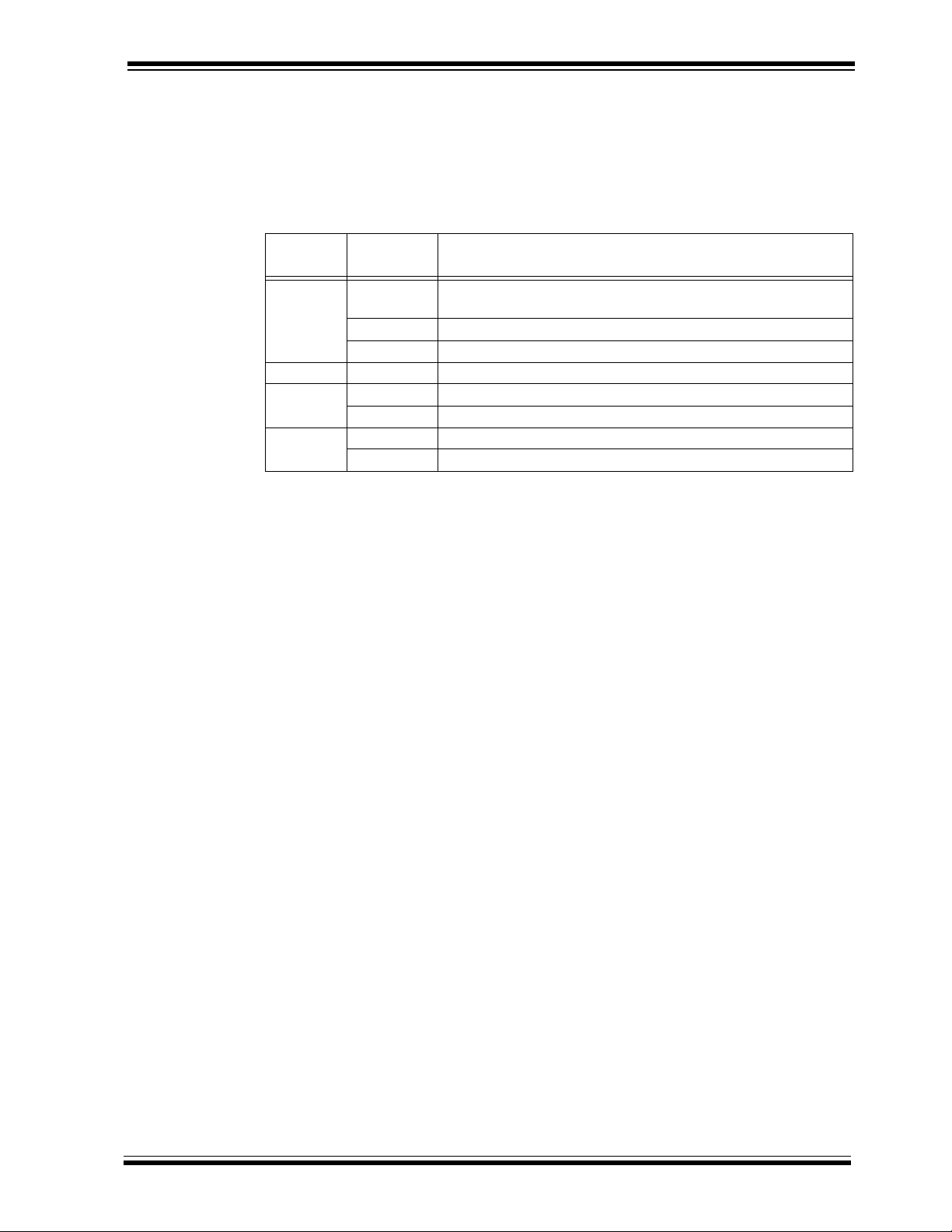
Table 66-1: SD A/D Module Functions by Registers and Bits
SD A/D
Function
Input SDxCON1 PWRLVL, SDREFP, SDREFN, VOSCAL, DITHER<1:0>,
Timing SDxCON3 SDCS<1:0>, SDDIV<2:0>
Conversion SDxCON1 SDON, SDSIDL
Output SDxCON2 RNDRES<1:0>, SDWM<1:0>
The following steps should be followed for performing an SD A/D conversion.
1. Configure the SD A/D module:
a) Select the power l evel
b) Select the volta ge reference sou rce to match th e expected rang e on the ana log inputs
c) Set the dither value
d) Set the gain
e) Select the output resolution
f) Select the Data Overwrite mode
g) Select the Chopping Clock mode
h) Select the input channel
i) Select the SD A/D module clock source
j) Select the desired output data rate
k) Select the sampling frequency
2. Configure the SD A/D interrupt (if required):
a) Select the Interrupt mode
b) Clear the SDAxIF bit
c) Select the SD A/D interrupt priority
3. Turn on the SD A/D module.
The options for each co nfiguratio n step are des cribed in th e subseque nt section s. Example 66-1
shows the possible initialization sequence.
Register(s) Specific Bits
SDGAIN<2:0>
SDxCON2 CHOP<1:0>
SDxCON3 SDCH<2:0>
SDxCON2 SDINT<1:0>
SDxCON3 SDOSR<2:0>
DS30687A-page 66-8 © 2013 Microchip Technology Inc.
Page 9

Section 66. 16-Bit Sigma-Delta A/D Converter
signed short int count;
signed short int result;
// Configure the SD A/D module
SD1CON1bits.PWRLVL = 0; // Low power, normal bandwidth
SD1CON1bits.SDREFP = 0; // Positive Voltage Reference is SVDD
SD1CON1bits.SDREFN = 0; // Negative Voltage Reference is SVSS
SD1CON1bits.VOSCAL = 0; // Internal Offset Measurement is disabled
SD1CON1bits.DITHER = 1; // Low Dither
SD1CON1bits.SDGAIN = 0; // Gain is 1:1
SD1CON2bits.RNDRES = 2; // Round result to 16-bit
SD1CON2bits.SDWM = 1; // SDxRESH/SDxRESL updated on every Interrupt
SD1CON2bits.CHOP = 3; // Chopping should be enabled
SD1CON3bits.SDCH = 0; // Channel 0 (see the specific device data sheet)
SD1CON3bits.SDCS = 1; // Clock Source is a 8 MHz FRC
SD1CON3bits.SDOSR = 0; // Oversampling Ratio (OSR) is 1024 (best quality)
SD1CON3bits.SDDIV = 1; // Input Clock Divider is 2 (SD ADC clock is 4MHz)
// Configure SD A/D interrupt
SD1CON2bits.SDINT
= 3; // Interrupt on every data output
IFS6bits.SDA1IF
= 0; // Clear interrupt flag
// Turn on the SD A/D module
SD1CON1bits.SDON = 1;
// Wait for a minimum of five interrupts to be generated. Need to throw at least
// the first four away when using interrupt every period option, since the
// low pass SINC filter needs to be flushed with new data when we change
// ADC channel or initialize the ADC.
for(count=0; count<8; count++)
{
//Clear interrupt flag.
IFS6bits.SDA1IF = 0;
//Wait for the result ready.
while(IFS6bits.SDA1IF == 0);
}
// Channel #0 conversion result.
result = SD1RESH;
Example 66-1: Channel Measurement
66
16-Bit Sigma-De lt a
A/D Converter
66.3.1 Selecting the Voltage Reference Source
The voltage references for SD A/D conversions are selected using the SDREFN and SDREFP
control bits (SDx CON1 <2:1 >). T he upper voltage refe ren ce (V
applied on the SV
applied on the SV
© 2013 Microchip Technology Inc. DS30687A-page 66-9
REF+ pin. The lower voltage reference (VREF-) can be SVSS or the voltage
REF- pin.
REF+) can be SVDD or the voltag e
Page 10

PIC24F Family Reference Manual
SINC
3
Low-Pass
Filter
SDOSR<2:0>
SDDIV<2:0>
Primary
Oscillator
FRC
FCY
SDCS<1:0>
1/4
SDxRESH
SDxRESHL
Sampling
Circuit
Modulator
-
Prescaler
SDCLK
OSR Select
66.3.2 Gain C o n tr o l
The Programmable Gain Amplifier (PGA) block can be used to amplify very low signals, but the
differential in put range of the SD A/D module shou ld not be excee ded to avoid a sa turated output
result code. The PGA is controlled by the SDGAIN<2:0> bits in the SDxCON1 register.
Table 66-2 shows the PGA configuration settings.
Table 66-2: PGA Configuration Setting
SDGAIN<2:0>
000 1 0 ± |Reference|
001 2 6 ± (|Reference| /2)
010 4 12 ± (|Reference| /4)
011 8 18 ± (|Reference| /8)
100 16 24 ± (|Reference| /16)
101 32 30 ± (|Reference| /32)
66.3.2.1 SELECTION OF ANALOG AMPLIFIER BANDWIDTH
Setting the PWRLVL bit in the SDxCON1 register improves the bandwi d th and response time of
the input amplifier, but at the cost of consuming more power. Smaller response time decreases
the settling error in amplifier stages, and thereby, improves harmonic distortions. The PWRLVL
bit can be cleared to save power.
Gain
(V/V)
Gain
(dB)
Differential V
IN Range (V)
66.3.3 Selecting the SD A/D Module Clock Source
The clock source to the SD A/D Converter (SDCLK) can be one of the following three possible
clocks:
• Primary Oscillator
•FRC (8 MHz)
• System Clock (F
The selection can be done using the SDCS<1:0> bits in the SDxCON3 register. The A/D
Converter source clock is divided inside of the module, as shown in Figure 66-2.
Figure 66-2: SD A/D Module Clocking Details
CY)
DS30687A-page 66-10 © 2013 Microchip Technology Inc.
Page 11

Section 66. 16-Bit Sigma-Delta A/D Converter
66.3.3.1 SELECTING THE SD A/D CONVERTER SAMPLING FREQUENCY AND
OUTPUT DATA RATE
The selected source clock (see SDCLK in Figure 66-2) is divided by the selected ratio determined by the SDDIV<2 :0> bit s in the SDx CON3 register. The resulting clock must be i n the range
of 1 MHz to 4 MHz.
The module clock is further divided by the s ele cte d ra tio determined by the SDOSR< 2:0> bits in
the SDxCON3 register . The result i s the rate at which the SD A/D outputs n ew data. To determine
the SDOSR<2:0> setting for the required output data rate, see Table 66-3.
Table 66-3: Data Rate Settings
Data Rate
(ksps)
62.500 4 110
31.2500
15.6250
7.8125
3.90625
1.953125
0.9765625
0.4883
0.2441 1 000
A/D Clock Frequency (MHz) SDOSR<2:0>
4 101
2 110
4 100
2 101
1 110
4 011
2 100
1 101
4 010
2 011
1 100
4 001
2 010
1 011
4 000
2 001
1 010
2 000
1 001
66
16-Bit Sigma-De lt a
A/D Converter
© 2013 Microchip Technology Inc. DS30687A-page 66-11
Page 12

PIC24F Family Reference Manual
66.3.4 Selection of Dither
Dithering helps in suppressing the Idle tones present in the SD A/D module. Dithering is the process of intentionally adding a small error to the SD A/D feedback loop in order to “decorrelate”
the outputs and “b reak ” the Idle tones’ behavior. The dithering process scrambles the Idle tone s
into baseband white noi se and ensures th at dynamic parame ters (SNR, SINAD, THD, SF DR) are
less signal dependent.
The baseband white noise can then be filtered and averaged through the internally provided
hardware Oversampling Ratio (OSR) to achieve better result quality. It is therefore, generally
recommended to enable dithering in most applications. However, the optimum dithering setting
for a given application depends on the OSR selecte d and the relative volta ge of the applied A/D
reference to the SV
The higher OSR settings (e.g., 128 to 1024) are better at averaging the baseband white noise in troduced by dithering. At the higher OSR settings, enabling dithering improves overall performance
and is recommended. At lower OSR settings (e.g., 16 to 64), the averaging is not as effective and
the extra noise injected by dithering can potentially decrease the SNR, even though it may help to
suppress Idle tones. At the very low OSR settings, this results in a performance trade-off, and in
some cases (at very low OSR), it may be preferable to disable dithering. The dithering can be
enabled by the DITHER<1:0> bits in the SDxCON1 register.
66.3.5 Chop Clock Select Mode
Chopping Select bit s (C HOP<1:0 > bit s in the SDxCON 2 regis ter) are ma inly u sed to re move t he
1/f noise from the signal band in the modulator. To obtain 16-bit resolution, chopping should
always be enabled.
DD voltage.
66.3.6 SINC3 Filter and Rounding of Result
The SD A/D module includes a decimation filter that is a third-order SINC (or notch) filter. This
filter processes the multibit stream into 8, 16, 24 or 32-bit words (depending on the
RNDRES<1:0> bits in the SDxCON2 register). The settling time of the fil ter is three data rate periods. It is recommended to discard unsettled data. This can be done by polling the SDRDY bit in
the SDxCON2 register. The output of the SINC filter is padded with Least Significant zeros for
any resolution less than 32 bits.
66.3.7 Data Write Modes
The Write mode bits, SDWM<1:0> (SDxCON2) determine when the Result register is updated.
There are three options in Write mode:
• Result register is never updated (useful for the Threshold Compare feature)
• Res ult register is updated on every interrupt
• Result register is updated on every interrupt, after the SDRDY bit (SDxCON2<0>) is
cleared to ‘0’ in software
66.3.7.1 RESULT DATA READY
The conversion result value is valid only when the SDRDY bit (SDxCON2<0>) reads as ‘1’ and
the A/D module interrupt is generated. The SDRDY bit can only be cleared by software or on a
device Reset. If the user sets the SDWM<1:0> bits (SDxCON2<9:8>) to ‘00’, then the SD A/D
Converter does not update the Result register with the result until the SDRDY bit is cleared in
software.
If SDWM<1:0> = 01, then the SD A/D Converter updates the Result register, regardless of the
SDRDY bit.
DS30687A-page 66-12 © 2013 Microchip Technology Inc.
Page 13

Section 66. 16-Bit Sigma-Delta A/D Converter
66.3.7.2 SD A/D RESULT REGISTER
The SD A/D Converter result is stored in the SDxRESH:SDxRESL registers as a 32-bit
2’s complement signed number. When rounding is enabled (RNDRES<1:0> bits in the
SDxCON2 register), the Least Significant bits (LSbs) which are rounded off will read as ‘0’. Additionally, when operating the A/D at OSR values l ess than 1 024, not eno ugh dat a will be int ernall y
generated by the hardware to fi ll al l 3 2 bi ts of th e SDx R ES H/ S DxR E SL re gister pair. Therefore,
especially when operating at OSR values less than 1024, some of the LSbs will be fully meaningless and may read b ac k as static values. The Mos t Sig ni fic ant bits (MSbs) of the 32-b it result
will remain meaningful, but will be restricted by the result quality for a given OSR setting.
66.3.8 Input Channel Selection
The input analog channel can be selected usi ng the SDCH<2:0> bits in the SDxCON3 regi ster. The
SD A/D Converter comprises both single-ended and differential channels. The number of
single-ended and differential channels available is device-specific. For more information, refer to
the specific device data sheet. Each differential channel has inverting (CHn-) and non-inverting
inputs (CHn+). If any channel is not used, both CHn- and CHn+ should be connected to SV
Single-ended channels are available as the positive input to the SD A/D Converter. The negative
input for these channels will always be SVSS. This performs a single-ended conversion on the
selected channel. When performing single-ended conversions, the A/D module s till produces two’s
complement signed numbers. It is therefore possible for slightly negative number results to occur
due to offset error . The application firmware should ch eck for negative results, and tre at all negative
numbers as ‘0’, if true unsigned single-ended behavior is desired. The module also facilitates a
dedicated differential channel used for gain error measurements. For more information on gain
error measurements, see Section 66.6 “Gain Error Calibration”.
SS.
66
16-Bit Sigma-De lt a
A/D Converter
66.3.9 Channel Switching
When the channel is switched, five data rate clocks are required to flush the previous contents
from the SINC
The results c an ha ve residual volta ge information from th e p r evious selected chan nel due to the
low-pass filtering effect of the SINC filter. Therefore, it is recommended to select an interrupt on
every fifth d ata output by setting the SDINT<1:0 > bits to ‘10’, and upon first interrupt, the require d
interrupt can be selected.
3
filter (low-pass filter). During this time, the results generated may not be valid.
66.3.10 Enabling the Module
The SD A/D is enabl ed by s ett ing the SDON bit (SDxC ON1 <15> ) to ‘ 1’. Af te r SDON i s set to ‘1’,
the module requires a power-up analog settling time of about 10 µs, during which time, the A/D
Converter may not gen erate ac curate results . The appl icatio n firmwa re should theref ore thro w
away the initial results associated with the analog settling time and the time it takes to flush the
low-pass SINC filter with new data. When SDON is set to ‘0’, the module is disabled; the digital
and analog portions of the module are turned off for maximum current savings.
The module should be configured to the required settings and the SDRDY bit (SDxCON2<0>)
should be cleared before turning on the SD A/D.
Note: When the module is enabled (SDON = 1), the firmware may change the channel
selection (SDCH<2:0> or VOSCAL bit settings). If other A/D module settings must
be changed, the module should be disabled first (SDON = 0).
© 2013 Microchip Technology Inc. DS30687A-page 66-13
Page 14

PIC24F Family Reference Manual
Offset Corrected Result = (New SDxRES Result) – (VOSCAL Result)
66.4 INTERRUPT MODES
There are four Interrupt modes:
• Interrupt on Every Data Ready mode
• Interrupt on every Fifth Data Ready mode
• Interrupt on Threshold Current Value Lesser than the Previous Value mode
• Interrupt on Threshold Current Value Greater than the Previous Value mode
The four modes are controlled by the SDINT<1:0> bits in the SDxCON2 register.
66.4.1 Interrupt on Every Data Ready
This mode is use ful af ter the first dat a is read. No te that the frequenc y of the dat a rate cl ock mu st
be less than F
66.4.2 Interrupt on Every Fifth Data Ready
This mode is useful immediat ely afte r the module is enabled, wh en the inpu t channel is switch ed
or when the device wake s up from Sle ep. The mo dule t akes five dat a rate cl ocks for flushi ng old
values from the SINC3 filter.
66.4.3 Interrupt on Threshold Compare
The SDINT<1:0> bits allow the user to have interrupts, only if the data coming out of the filter is
greater than, or less than, the value currently in the Result register. If the user wishes to retain
the threshold value, the SDWM<1:0> bits must be set to ‘10’. If SDWM<1:0> are set to ‘01’ or
‘00’, the threshold compare function turns into a “find the lowest/highest sampled value” type of
operation.
CY/2 to avoid missing the samples.
66.5 OFFSET CALIBRATION
The SD A/D module includes a feature for measuring internal offset error. Application firmware
can enable this feature by fully configuring the A/D module and setting the VOSCAL bit in the
SDxCON1 register.
When the VOSCAL bit is set, the A/D module ignores the currently selected SDCH<2:0> channel
select bits, and instead, performs conversions on an internal channel that generates
SDxRESH/SDxRESL results which represent the offset error of the A/D Converter. After the
SINC filter delay has bee n satisfie d, the applic ation firmw are shoul d save the resu lt value (w hich
will be formatted a s a s ign ed two’s complem ent value, the same as n orm al A/D m odule results).
After the offs et error measurement result data ha s been saved, th e application fi rmware can clear
the VOSCAL bit to switch the A/D module back into Normal Channel Measurement mode.
The application firmware can then correct for offset error in subsequent analog channel
measurements by subtracting the offset error value from all future results. Equation 66-1 shows
the method for correcting offset error.
Equation 66-1: Correcting Offset Error
Example 66-2 shows a example C code for the offset calibration.
DS30687A-page 66-14 © 2013 Microchip Technology Inc.
Page 15

Section 66. 16-Bit Sigma-Delta A/D Converter
Legend:
G
ECF
= Floating-point gain error correction factor
ADRES
EXPECTED
= The expected A/D result (with no offset or gain error) based on the
applied input voltage. When the A/D is configured to measure the references in 1x Gain
mode, the expected result is 32767.
ADRES
RAW
= The raw , unco rrected 1 6-bit s igned result read from the SDxRESH re giste r.
ADRES
VOSCAL
= The 16-bit value representing the offset error measured with the A/D
“VOSCAL” feature.
G
ECF
ADRES
EXPECTED
ADRES
RAW
ADRES
VOSCAL
–
-------------------------------------------------------------------------- -=
66.6 GAIN ERROR CALIBRATION
The SD A/D module has a dedicated channel for gain error measurements. Selecting this
channel allows the module to internally sample the reference voltages as an input to the A/D
Converter. In theory, if the A/D module has no offset or gain error, this always generates an
SDxRESH result of 32767 (maximum full-scale value). In practice, it is normal for a real world
Sigma-Delta A/D to have a significant, but highly correctable, gain error. In this design, the A/D
Converter has a gai n error, which will cause the A/D Conv erter to generat e a result that is somewhat less than the theoretical 32767 full-scale result value. Gain error varies depending on the
SDGAIN<2:0> bits (SDxCON1<10:8>) selection, and some part, to part variations. Equation 66-2
shows the method for calculating a floating-point “gain error correction factor”, which can be
multiplied against subsequent result values to com pensate for gai n error.
Equation 66-2: G ain Error Correction Factor
66
16-Bit Sigma-De lt a
A/D Converter
Example 66-2 shows the proces s to perform a channel measurement, which uses offset correction
and gain error correction to compute a fully calibrated result value.
66.6.1 Considerations for Gain Error
The following needs to be considered for gain error correction:
1. Gain error of the A/D Converter can be measured by intentionally inputting a well-known
analog voltag e and comp aring the outpu t result code w ith the theoret ically expe cted result
code.
2. If the V
3. Due to the internal g ain error of the A/D design, th e actual val ue will be les s than full scale.
4. A floating-point gain error correc tion factor ca n be compute d using the raw A/D Con verter
5. Once the gain error correction factor is known, it can be saved in the firmware. While
REF+/VREF- reference sources are measured (with a gain setting of 1), the result
code should theoretically be full scale (e.g., 32767).
result (e.g., when measuring the references) and the expected result, as shown in
Example 66-2.
carrying out A/D Converter measurements on other channels/input voltage sources, the
gain error correction factor can be multiplied by the raw result (after offset correction
through VOSCAL) to compensate for the A/D Converter gain error.
© 2013 Microchip Technology Inc. DS30687A-page 66-15
Page 16

PIC24F Family Reference Manual
unsigned char count;
signed short int offset;
signed long int maxValue;
const double expectedMaxValue = 32767; // 0x7FFF
double gain;
signed long int channelValue;
double calibratedResult;
// ADC initialization.
SD1CON1bits.PWRLVL = 0; // Low power, normal bandwidth
SD1CON1bits.SDREFP = 0; // Positive Voltage Reference is SVDD
SD1CON1bits.SDREFN = 0; // Negative Voltage Reference is SVSS
SD1CON1bits.VOSCAL = 1; // Internal Offset Measurement Enable
SD1CON1bits.DITHER = 1; // Low Dither
SD1CON1bits.SDGAIN = 0; // Gain is 1:1
SD1CON2bits.RNDRES = 2; // Round result to 16-bit
SD1CON2bits.SDWM = 1; // SDxRESH/SDxRESL updated on every Interrupt
SD1CON2bits.SDINT = 3; // Interrupt on every data output
SD1CON2bits.CHOP = 3; // Chopping should be enabled
SD1CON3bits.SDCH = 0; // Channel 0 (see the specific device data sheet)
SD1CON3bits.SDCS = 1; // Clock Source is a 8 MHz FRC
SD1CON3bits.SDOSR = 0; // Oversampling Ratio (OSR) is 1024 (best quality)
SD1CON3bits.SDDIV = 1; // Input Clock Divider is 2 (SD ADC clock is 4MHz)
// Enable ADC.
SD1CON1bits.SDON = 1;
// Wait for a minimum of five interrupts to be generated. Need to throw at least
// the first four away when using interrupt every period option, since the
// low pass SINC filter needs to be flushed with new data when we change
// ADC channel or initialize the ADC.
for(count=0; count<8; count++)
{
//Clear interrupt flag.
IFS6bits.SDA1IF = 0;
//Wait for the result ready.
while(IFS6bits.SDA1IF == 0);
}
// Save the initial VOSCAL offset value from the ADC.
// This value will be used to correct the offset error for all
// subsequent ADC measurements.
offset = SD1RESH;
// Configure ADC for normal operation.
SD1CON1bits.VOSCAL = 0;
// Measures the reference selected by SDREFP/SDREFN
// (see the specific device data sheet).
SD1CON3bits.SDCH = 3;
Example 66-2: Channel Conversion with Offset and Gain Correction
DS30687A-page 66-16 © 2013 Microchip Technology Inc.
Page 17

Section 66. 16-Bit Sigma-Delta A/D Converter
// Wait for a minimum of five interrupts to be generated.
for(count=0; count<8; count++)
{
//Clear interrupt flag.
IFS6bits.SDA1IF = 0;
//Wait for the result ready.
while(IFS6bits.SDA1IF == 0);
}
// Save the maximum value to calculate the gain.
maxValue = (signed short int) SD1RESH;
// Calculate gain.
gain = expectedMaxValue/((double)(maxValue-offset));
// Select channel #0 for the measurement.
// (see the specific device data sheet).
SD1CON3bits.SDCH = 0;
// Adjust loop end value for desired settling time (value must be >= 5).
for(count=0; count<8; count++)
{
// Clear interrupt flag.
IFS6bits.SDA1IF = 0;
// Wait for the result ready.
while(IFS6bits.SDA1IF == 0);
}
// Not corrected channel #0 result.
channelValue = (signed short int) SD1RESH;
// Correct offset.
channelValue -= offset;
// Correct gain.
calibratedResult = gain*channelValue;
Example 66-2: Channel Conversion with Offset and Gain Correction (Continued)
66
16-Bit Sigma-De lt a
A/D Converter
© 2013 Microchip Technology Inc. DS30687A-page 66-17
Page 18

PIC24F Family Reference Manual
1.2345 1.2345 2182
18
=
1.23456 1.23456 262144 262144 323623 262144=
// This is fixed point location
#define FIXED_POINT_POS 15
unsigned char count;
signed long int offset;
signed long int maxValue;
signed long int expectedMaxValue;
signed long int gain;
signed long int channelValue;
signed short int calibratedResult;
// ADC initialization.
SD1CON1bits.PWRLVL = 0; // Low power, normal bandwidth
SD1CON1bits.SDREFP = 0; // Positive Voltage Reference is SVDD
SD1CON1bits.SDREFN = 0; // Negative Voltage Reference is SVSS
SD1CON1bits.VOSCAL = 1; // Internal Offset Measurement Enable
SD1CON1bits.DITHER = 1; // Low Dither
SD1CON1bits.SDGAIN = 0; // Gain is 1:1
SD1CON2bits.RNDRES = 2; // Round result to 16-bit
SD1CON2bits.SDWM = 1; // SDxRESH/SDxRESL updated on every Interrupt
SD1CON2bits.SDINT = 3; // Interrupt on every data output
SD1CON2bits.CHOP = 3; // Chopping should be enabled
SD1CON3bits.SDCH = 0; // Channel 0 (see the specific device data sheet)
SD1CON3bits.SDCS = 1; // Clock Source is a 8 MHz FRC
SD1CON3bits.SDOSR = 0; // Oversampling Ratio (OSR) is 1024 (best quality)
SD1CON3bits.SDDIV = 1; // Input Clock Divider is 2 (SD ADC clock is 4MHz)
66.6.2 Gain Error Correction Using Integer Math
Floating-point math is easy and convenient to use, but is often undesirable during actual
execution because it generally consumes a large amount of CPU execution time and code space
to perform. Fortunately, it is possible to correct for A/D gain error using pure in teger-base d math.
In mathematical theory, if an expression is multiplied by a cons tan t and then di vided by the same
constant, the expression stays the same (Equation 66-3).
Equation 66-3: Math Example
In this example, mul tiplying an d divid ing by a co nst ant number (218 or 262144) does n ot ch ange
the value of the expre ssio n. U sing t his approach, it is possible to c on vert floa tin g-point numbers
into integers with minimal truncation error (Equation 66-4).
Equation 66-4: Converting Floating Point Number into Integer Example
The final expression (323623/262144) is very easy and quick to evaluate by the microcontroller
during run time, as it is equ ivalent to taki ng a 32-bit integer and arithmetically shif ting it to the right
by 18 bit positions (equivalent to dividing by 262144). This mathematical principle can therefore
be used to perform traditional floating-point math operations, using integer math with very little
error, provided that the constant number being multiplied and divided by is a very large number
18
(ex: 2
Sigma-Delta A/D gain error quickly during application run time.
or larger). Example 66-3 shows how this principle can be used to correct for the
Example 66-3: Channel Conversion with Offset and Gain Correction Using Integer Math
DS30687A-page 66-18 © 2013 Microchip Technology Inc.
Page 19

Section 66. 16-Bit Sigma-Delta A/D Converter
// Enable ADC
SD1CON1bits.SDON = 1;
// Wait for a minimum of five interrupts to be generated. Need to throw at least
// the first four away when using interrupt every period option, since the
// low pass SINC filter needs to be flushed with new data when we change
// ADC channel or initialize the ADC.
for(count=0; count<8; count++)
{
//Clear interrupt flag.
IFS6bits.SDA1IF = 0;
//Wait for the result ready.
while(IFS6bits.SDA1IF == 0);
}
// Save the initial VOSCAL offset value from the ADC.
// This value will be used to correct the offset error for all
// subsequent ADC measurements.
offset = (signed short int)SD1RESH;
// Configure ADC for normal operation.
SD1CON1bits.VOSCAL = 0;
// Measures the reference selected by SDREFP/SDREFN
// (see the specific device data sheet).
SD1CON3bits.SDCH = 3;
// Wait for a minimum of five interrupts to be generated.
for(count=0; count<8; count++)
{
//Clear interrupt flag.
IFS6bits.SDA1IF = 0;
//Wait for the result ready.
while(IFS6bits.SDA1IF == 0);
}
// Save the maximum value to calculate the gain.
maxValue = (signed short int)SD1RESH;
// Correct offset.
maxValue -= offset;
// Calculate gain.
expectedMaxValue = ((signed long int)32767)<<FIXED_POINT_POS;
gain = expectedMaxValue/maxValue;
// Select channel #0 for the measurement.
// (see the specific device data sheet).
SD1CON3bits.SDCH = 0;
Example 66-3: Channel Conversion with Offset and Gain Correction Using Integer Math (Continued)
66
16-Bit Sigma-De lt a
A/D Converter
© 2013 Microchip Technology Inc. DS30687A-page 66-19
Page 20

PIC24F Family Reference Manual
// Adjust loop end value for desired settling time (value must be >= 5).
for(count=0; count<8; count++)
{
// Clear interrupt flag.
IFS6bits.SDA1IF = 0;
// Wait for the result ready.
while(IFS6bits.SDA1IF == 0);
}
// Not corrected channel #0 result.
channelValue = (signed short int)SD1RESH;
// Correct offset.
channelValue -= offset;
// Correct gain.
channelValue = gain*channelValue;
// 16-bit signed result
calibratedResult = channelValue>>FIXED_POINT_POS;
Example 66-3: Channel Conversion with Offset and Gain Correction Using Integer Math (Continued)
DS30687A-page 66-20 © 2013 Microchip Technology Inc.
Page 21

Section 66. 16-Bit Sigma-Delta A/D Converter
66.7 OPERATION DURING SLEEP AND IDLE MODES
The SD A/D module supports the following power modes:
• Idle mode
• Sleep mode
66.7.1 Idle Mode
The SDSIDL bit (SDxCON1<13>) determines whether the module st op s or continu es operatio n in
Idle mode. If SDSIDL = 0, the module will continue normal operation when the device enters Idle
mode. If the SD A/D interrupt is enabled (SDAxIE = 1), the device will wake-up from Idle mode
when the SD A/D Interrupt Flag (SDAxIF = 1) occurs. Program execution will resume at the SD A/D
Interrupt Service Routine (ISR) if the SD A/D interrupt is greater than the current CPU priority.
Otherwise, execution will continue from the instruction after the PWRSAV #IDLE instruction (or
Idle();) that placed the device in Idle mode.
If SDSIDL = 1, the module will stop in Idle. If the device enters Idle mode in the middle of a
conversion, the conversion is aborted. The converter will not resume a partially completed
conversion on exiting from Idle mode.
66.7.2 Sleep Mode
If the device enters Sleep mode while the module is operating, the module will be suspended in
its current state until clock execution resumes. The output value will retain the last value before
Sleep.
66
16-Bit Sigma-De lt a
A/D Converter
66.8 EFFECTS OF A RESET
A device Reset forces all registers to their Reset state. This forces the SD A/D module to be
turned off and an y conve rsion in pro gress to b e aborted. Al l pins tha t are multi plexed wit h analo g
inputs will be configured as analog inputs. The corresponding TRIS bits will be set to ‘1’.
66.8.1 Use of SDRST
With the SDON bit set, the SDRST bi t ca n be us ed for the module to switch between activ e an d
inactive modes quickly, without any delay that is associated with the SDON bit.
© 2013 Microchip Technology Inc. DS30687A-page 66-21
Page 22

© 2013 Microchip Technology Inc. page 66-22
66.9 REGISTER MAP
Table 66-4: SD A/D Converter Register Map
File Name Bit 15 Bit 14 Bit 13 Bit 12 Bi t 11 Bit 10 Bit 9 Bit 8 Bit 7 Bit 6 Bit 5 B it 4 Bit 3 Bit 2 Bit 1 Bit 0
SDxCON1 SDON
SDxCON2 CHOP1 CHOP0 SDINT1 SDINT0
SDxCON3 SDDIV2 SDDIV1 SDDIV0 SDOSR2 SDOSR1 SDOSR0 SDCS1 SDCS0
SDxRESH Sigma-Delta A/D Result Register (bits 31-16) 0000
SDxRESL Sigma-Delta A/D Result Register (bits 15-0) 0000
Legend: — = unimplemented, read as ‘0’. Reset values are shown in hexadecimal.
— SDSIDL SDRST r SDGAIN2 SDGAIN1 SDGAIN0 DITHER1 DITHER0 —VOSCAL— SDREFN SDREFP PWRLVL 0000
— —SDWM1SDWM0— — — RNDRES1 RNDRES0 — — SDRDY 0000
— — — — — SDCH2 SDCH1 SDCH0 0000
Resets
PIC24F Family Reference Manual
All
Page 23

66.10 DESIGN TIPS
Question 1: Can we scan more than one channel?
Answer: Yes. However, it is recommended that you “flush” the pipeline before moving to the
next channel or the result will be erroneous.
Section 66. 16-Bit Sigma-Delta A/D Converter
66
16-Bit Sigma-De lt a
A/D Converter
© 2013 Microchip Technology Inc. DS30687A-page 66-23
Page 24

PIC24F Family Reference Manual
66.11 RELATED APPLICATION NOTES
This section lists application notes that are related to this section of the manual. These
application notes may not be written specifically for the PIC24F device family, but the concepts
are pertinent and could be used with modification and possible limitations. The current
application notes related to the 16-Bit A/D Converter module are:
Title Application Note #
Designing with the MCP3901 Dual Channel Analog-to-Digital Converters AN1300
Note: Please visit the Microchip web site (www.microchip.com) for additional application
notes and code examples for the PIC24F family of dev ices.
DS30687A-page 66-24 © 2013 Microchip Technology Inc.
Page 25

Section 66. 16-Bit Sigma-Delta A/D Converter
66.12 REVISION HISTORY
Revision A (April 2013)
This is the initial released revision of this document.
66
16-Bit Sigma-De lt a
A/D Converter
© 2013 Microchip Technology Inc. DS30687A-page 66-25
Page 26

PIC24F Family Reference Manual
NOTES:
DS30687A-page 66-26 © 2013 Microchip Technology Inc.
Page 27

Note the following details of the code protection feature on Microchip devices:
YSTEM
CERTIFIED BY DNV
== ISO/TS 16949 ==
• Microchip products meet the specification contained in their particular Microchip Data Sheet.
• Microchip believes that its family of products is one of the most secure families of its kind on the market t oday, when used in the
intended manner and under normal conditions.
• There are dishonest and possibly illegal methods used to breach the code protection feature. All of these methods, to our
knowledge, require using the Microchip products in a manner outside the operating specifications contained in Microchip’s Data
Sheets. Most likely, the person doing so is engaged in theft of intellectual property.
• Microchip is willing to work with the customer who is concerned about the integrity of their code.
• Neither Microchip nor any other semiconductor manufacturer can guarantee the security of their code. Code protection does not
mean that we are guaranteeing the product as “unbreakable.”
Code protection is constantly evolving. We at Microchip are com mitted to continuously improving the c ode prot ection f eatures of our
products. Attempts to break Microchip’s code protection feature may be a violation of t he Digit al Mill ennium Copyright Act. If such act s
allow unauthorized access to your software or other copyrighted work, you may have a right to sue for relief under that Act.
Information contained in this publication regarding device
applications and t he lik e is provided only for your convenience
and may be su perseded by updat es . I t is y our responsibility to
ensure that your application meets with your specifications.
MICROCHIP MAKES NO REPRESENTATIONS OR
WARRANTIES OF ANY KIND WHETHER EXPRESS OR
IMPLIED, WRITTEN OR ORAL, STATUTORY OR
OTHERWISE, RELATED TO THE INFORMATION,
INCLUDING BUT NOT LIMITED TO ITS CONDITION,
QUALITY, PERFORMANCE, MERCHANTABILITY OR
FITNESS FOR PURPOSE. Microchip disclaims all liability
arising from this information and its use. Use of Microchip
devices in life supp ort and/or safety ap plications is entir ely at
the buyer’s risk, and the buyer agrees to defend, indemnify and
hold harmless M icrochip from any and all dama ges, claims,
suits, or expenses re sulting from such use. No licens es are
conveyed, implicitly or otherwise, under any Microchip
intellectual property rights.
Trademarks
The Microchip name and logo, the Microchip logo, dsPIC,
FlashFlex, K
PICSTART, PIC
and UNI/O are registered trademarks of Microchip T echnology
Incorporated in the U.S.A. and other countries.
FilterLab, Hampshire, HI-TECH C, Linear Active Thermistor,
MTP, SEEVAL and The Embedded Control Solutions
Company are registered trademarks of Microchip Technology
Incorporated in the U.S.A.
Silicon Storage Technology is a registered trademark of
Microchip Technology Inc. in other countries.
Analog-for-the-Digital Age, Application Maestro, BodyCom,
chipKIT, chipKIT logo, CodeGuard, dsPICDEM,
dsPICDEM.net, dsPICworks, dsSPEAK, ECAN,
ECONOMONITOR, FanSense, HI-TIDE, In-Circuit Serial
Programming, ICSP, Mindi, MiWi, MPASM, MPF, MPLAB
Certified logo, MPLIB, MPLINK, mTouch, Omniscient Code
Generation, PICC, PICC-18, PICDEM, PICDEM.net, PICkit,
PICtail, REAL ICE, rfLAB, Select Mode, SQI, Serial Quad I/O,
Total Endurance, TSHARC, UniWinDriver, WiperLock, ZENA
and Z-Scale are trademarks of Microchip Technology
Incorporated in the U.S.A. and other countries.
SQTP is a service mark of Microchip T echnology Incorporated
in the U.S.A.
GestIC and ULPP are registered trademarks of Microchip
Te c hnology Germ any II GmbH & C o. KG, a subsidiary of
Microchip T echnology Inc., in other countries.
All other trademarks mentioned herein are property of their
respective companies.
© 2013, Microchip Technology Incorporated, Printed in the
U.S.A., All Rights Reserved.
Printed on recycled paper.
ISBN: 978-1-62077-164-8
EELOQ, KEELOQ logo, MPLAB, PIC, PICmicro,
32
logo, rfPIC, SST, SST Logo, SuperFlash
QUALITY MANAGEMENT S
2013 Microchip Technology Inc. DS30687A-page 66-27
Microchip received ISO/TS-16949:2009 certification for its worldwide
headquarters, design and wafer fabrication facilities in Chandler and
Tempe, Arizona; Gresham, Oregon and design centers in California
and India. The Company’s quality system processes and procedures
are for its PIC
devices, Serial EEPROMs, microperipherals, nonvolatile memory and
analog products. In addition, Microchip’s quality system for the design
and manufacture of development systems is ISO 9001:2000 certified.
®
MCUs and dsPIC® DSCs, KEELOQ
®
code hopping
Page 28

Worldwide Sales and Service
AMERICAS
Corporate Office
2355 West Chandler Blvd.
Chandler, AZ 85224-6199
Tel: 480-792-7200
Fax: 480-792-7277
Te chn ic al Support:
http://www.microchip.com/
support
Web Address:
www.microchip.com
Atlanta
Duluth, GA
Tel: 678-957-9614
Fax: 678-957-1455
Boston
Westborough, MA
Tel: 774-760-0087
Fax: 774-760-0088
Chicago
Itasca, IL
Tel: 630-285-0071
Fax: 630-285-0075
Cleveland
Independence, OH
Tel: 216-447-0464
Fax: 216-447-0643
Dallas
Addison, TX
Tel: 972-818-7423
Fax: 972-818-2924
Detroit
Farmington Hills, MI
Tel: 248-538-2250
Fax: 248-538-2260
Indianapolis
Noblesville, IN
Tel: 317-773-8323
Fax: 317-773-5453
Los Angeles
Mission Viejo, CA
Tel: 949-462-9523
Fax: 949-462-9608
Santa Clara
Santa Clara, CA
Tel: 408-961-6444
Fax: 408-961-6445
Toronto
Mississauga, Ontario,
Canada
Tel: 905-673-0699
Fax: 905-673-6509
ASIA/PACIFIC
Asia Pacific Office
Suites 3707-14, 37th Floor
Tower 6, The Gateway
Harbour City, Kowloon
Hong Kong
Tel: 852-2401-1200
Fax: 852-2401-3431
Australia - Sydney
Tel: 61-2-9868-6733
Fax: 61-2-9868-6755
China - Beijing
Tel: 86-10-8569-7000
Fax: 86-10-8528-2104
China - Chengdu
Tel: 86-28-8665-5511
Fax: 86-28-8665-7889
China - Chongqing
Tel: 86-23-8980-9588
Fax: 86-23-8980-9500
China - Hangzhou
Tel: 86-571-2819-3187
Fax: 86-571-2819-3189
China - Hong Kong SAR
Tel: 852-2943-5100
Fax: 852-2401-3431
China - Nanjing
Tel: 86-25-8473-2460
Fax: 86-25-8473-2470
China - Qingdao
Tel: 86-532-8502-7355
Fax: 86-532-8502-7205
China - Shanghai
Tel: 86-21-5407-5533
Fax: 86-21-5407-5066
China - Shenyang
Tel: 86-24-2334-2829
Fax: 86-24-2334-2393
China - Shenzhen
Tel: 86-755-8864-2200
Fax: 86-755-8203-1760
China - Wuhan
Tel: 86-27-5980-5300
Fax: 86-27-5980-5118
China - Xian
Tel: 86-29-8833-7252
Fax: 86-29-8833-7256
China - Xiamen
Tel: 86-592-2388138
Fax: 86-592-2388130
China - Zhuhai
Tel: 86-756-3210040
Fax: 86-756-3210049
ASIA/PACIFIC
India - Bangalore
Tel: 91-80-3090-4444
Fax: 91-80-3090-4123
India - New Delhi
Tel: 91-11-4160-8631
Fax: 91-11-4160-8632
India - Pune
Tel: 91-20-2566-1512
Fax: 91-20-2566-1513
Japan - Osaka
Tel: 81-6-6152-7160
Fax: 81-6-6152-9310
Japan - Tokyo
Tel: 81-3-6880- 3770
Fax: 81-3-6880-3771
Korea - Daegu
Tel: 82-53-744-4301
Fax: 82-53-744-4302
Korea - Seoul
Tel: 82-2-554-7200
Fax: 82-2-558-5932 or
82-2-558-5934
Malaysia - Kuala Lumpur
Tel: 60-3-6201-9857
Fax: 60-3-6201-9859
Malaysia - Penang
Tel: 60-4-227-8870
Fax: 60-4-227-4068
Philippines - Manila
Tel: 63-2-634-9065
Fax: 63-2-634-9069
Singapore
Tel: 65-6334-8870
Fax: 65-6334-8850
Tai wan - Hsin Chu
Tel: 886-3-5778-366
Fax: 886-3-5770-955
Taiwan - Kaohsiung
Tel: 886-7-213-7828
Fax: 886-7-330-9305
Taiwan - Taipei
Tel: 886-2-2508-8600
Fax: 886-2-2508-0102
Thailand - Bangkok
Tel: 66-2-694-1351
Fax: 66-2-694-1350
EUROPE
Austria - Wels
Tel: 43-7242-2244-39
Fax: 43-7242-2244-393
Denmark - Copenhagen
Tel: 45-4450-2828
Fax: 45-4485-2829
France - Paris
Tel: 33-1-69-53-63-20
Fax: 33-1-69-30-90-79
Germany - Munich
Tel: 49-89-627-144-0
Fax: 49-89-627-144-44
Italy - Milan
Tel: 39-0331-742611
Fax: 39-0331-466781
Netherlands - Drunen
Tel: 31-416-690399
Fax: 31-416-690340
Spain - Madrid
Tel: 34-91-708-08-90
Fax: 34-91-708-08-91
UK - Wokingham
Tel: 44-118-921-5869
Fax: 44-118-921-5820
11/29/12
DS30687A-page 66-28 2013 Microchip Technology Inc.
 Loading...