

Page 1

PIC18F87J72
Evaluation Board
User’s Guide
© 2011 Microchip Technology Inc. DS51990A
Page 2

Note the following details of the code protection feature on Microchip devices:
• Microchip products meet the specification contained in their particular Microchip Data Sheet.
• Microchip believes that its family of products is one of the most secure families of its kind on the market today, when used in the
intended manner and under normal conditions.
• There are dishonest and possibly illegal methods used to breach the code protection feature. All of these methods, to our
knowledge, require using the Microchip products in a manner outside the operating specifications contained in Microchip’s Data
Sheets. Most likely, the person doing so is engaged in theft of intellectual property.
• Microchip is willing to work with the customer who is concerned about the integrity of their code.
• Neither Microchip nor any other semiconductor manufacturer can guarantee the security of their code. Code protection does not
mean that we are guaranteeing the product as “unbreakable.”
Code protection is constantly evolving. We at Microchip are committed to continuously improving the code protection features of our
products. Attempts to break Microchip’s code protection feature may be a violation of the Digital Millennium Copyright Act. If such acts
allow unauthorized access to your software or other copyrighted work, you may have a right to sue for relief under that Act.
Information contained in this publication regarding device
applications and the like is provided only for your convenience
and may be superseded by updates. It is your responsibility to
ensure that your application meets with your specifications.
MICROCHIP MAKES NO REPRESENTATIONS OR
WARRANTIES OF ANY KIND WHETHER EXPRESS OR
IMPLIED, WRITTEN OR ORAL, STATUTORY OR
OTHERWISE, RELATED TO THE INFORMATION,
INCLUDING BUT NOT LIMITED TO ITS CONDITION,
QUALITY, PERFORMANCE, MERCHANTABILITY OR
FITNESS FOR PURPOSE. Microchip disclaims all liability
arising from this information and its use. Use of Microchip
devices in life support and/or safety applications is entirely at
the buyer’s risk, and the buyer agrees to defend, indemnify and
hold harmless Microchip from any and all damages, claims,
suits, or expenses resulting from such use. No licenses are
conveyed, implicitly or otherwise, under any Microchip
intellectual property rights.
Trademarks
The Microchip name and logo, the Microchip logo, dsPIC,
K
EELOQ, KEELOQ logo, MPLAB, PIC, PICmicro, PICSTART,
32
PIC
logo, rfPIC and UNI/O are registered trademarks of
Microchip Technology Incorporated in the U.S.A. and other
countries.
FilterLab, Hampshire, HI-TECH C, Linear Active Thermistor,
MXDEV, MXLAB, SEEVAL and The Embedded Control
Solutions Company are registered trademarks of Microchip
Technology Incorporated in the U.S.A.
Analog-for-the-Digital Age, Application Maestro, chipKIT,
chipKIT logo, CodeGuard, dsPICDEM, dsPICDEM.net,
dsPICworks, dsSPEAK, ECAN, ECONOMONITOR,
FanSense, HI-TIDE, In-Circuit Serial Programming, ICSP,
Mindi, MiWi, MPASM, MPLAB Certified logo, MPLIB,
MPLINK, mTouch, Omniscient Code Generation, PICC,
PICC-18, PICDEM, PICDEM.net, PICkit, PICtail, REAL ICE,
rfLAB, Select Mode, Total Endurance, TSHARC,
UniWinDriver, WiperLock and ZENA are trademarks of
Microchip Technology Incorporated in the U.S.A. and other
countries.
SQTP is a service mark of Microchip Technology Incorporated
in the U.S.A.
All other trademarks mentioned herein are property of their
respective companies.
© 2011, Microchip Technology Incorporated, Printed in the
U.S.A., All Rights Reserved.
Printed on recycled paper.
ISBN: 978-1-61341-304-3
Microchip received ISO/TS-16949:2002 certification for its worldwide
headquarters, design and wafer fabrication facilities in Chandler and
Tempe, Arizona; Gresham, Oregon and design centers in California
and India. The Company’s quality system processes and procedures
are for its PIC
devices, Serial EEPROMs, microperipherals, nonvolatile memory and
analog products. In addition, Microchip’s quality system for the design
and manufacture of development systems is ISO 9001:2000 certified.
®
MCUs and dsPIC® DSCs, KEELOQ
®
code hopping
DS51990A-page 2 © 2011 Microchip Technology Inc.
Page 3

PIC18F87J72 EVALUATION BOARD
USER’S GUIDE
Table of Contents
Preface ........................................................................................................................... 5
Introduction............................................................................................................ 5
Document Layout .................................................................................................. 6
Recommended Reading........................................................................................ 7
The Microchip Web Site ........................................................................................ 7
Customer Support ................................................................................................. 8
Document Revision History ................................................................................... 8
Chapter 1. Product Overview
1.1 Introduction ..................................................................................................... 9
1.2 PIC18F87J72 Evaluation Board Functionality and Features .......................... 9
1.3 PIC18F87J72 EVALUATION BOARD KIT CONTENTS .............................. 10
Chapter 2. Hardware Description
2.1 Introduction ................................................................................................... 11
Chapter 3. PIC18F87J72 Evaluation Board Features
3.1 Introduction ................................................................................................... 17
Chapter 4. PIC18F87J72 Evaluation Board Firmware Flowchart
4.1 Introduction ................................................................................................... 23
Chapter 5. PIC18F87J72 Evaluation Board Lab Test Results
5.1 Introduction ................................................................................................... 31
Chapter 6. PIC18F87J72 Evaluation Board GUI
6.1 Introduction ................................................................................................... 35
© 2011 Microchip Technology Inc. DS51990A-page 3
Page 4

PIC18F87J72 EVALUATION BOARD USER’S GUIDE
Appendix A. Schematics and Layouts
A.1 Introduction .................................................................................................. 37
A.2 Board – Schematic 1 .................................................................................... 38
A.3 Board – Schematic 2 ................................................................................... 39
A.4 Board – Schematic 3 .................................................................................... 40
A.5 Board – Schematic 4 .................................................................................... 41
A.6 Board – PCB Front Page ............................................................................. 42
A.7 Board – PCB Top Silk ................................................................................. 43
A.8 Board – PCB Top Layer ............................................................................... 44
A.9 Board – PCB Bottom Layer .......................................................................... 45
A.10 Board – PCB Bottom Silk ........................................................................... 46
A.11 Board – PCB L1 Ground ............................................................................ 47
A.12 Board – PCB L2 VDD ................................................................................ 48
Appendix B. Bill of Materials (BOM)
Worldwide Sales and Service .....................................................................................52
DS51990A-page 4 © 2011 Microchip Technology Inc.
Page 5

PIC18F87J72 EVALUATION BOARD
USER’S GUIDE
Preface
NOTICE TO CUSTOMERS
All documentation becomes dated, and this manual is no exception. Microchip tools and
documentation are constantly evolving to meet customer needs, so some actual dialogs
and/or tool descriptions may differ from those in this document. Please refer to our web site
(www.microchip.com) to obtain the latest documentation available.
Documents are identified with a “DS” number. This number is located on the bottom of each
page, in front of the page number. The numbering convention for the DS number is
“DSXXXXXA”, where “XXXXX” is the document number and “A” is the revision level of the
document.
For the most up-to-date information on development tools, see the MPLAB
Select the Help menu, and then Topics to open a list of available on-line help files.
®
IDE on-line help.
INTRODUCTION
This chapter contains the general information that will be useful to know before using
the PIC18F87J72 Evaluation Board. Items discussed in this chapter include:
• Document Layout
• Recommended Reading
• The Microchip Web Site
• Customer Support
• Document Revision History
© 2011 Microchip Technology Inc. DS51990A-page 5
Page 6

PIC18F87J72 Evaluation Board User’s Guide
DOCUMENT LAYOUT
This document describes how to use the PIC18F87J72 Evaluation Board as a
development tool to emulate and debug firmware on a target board. The manual layout
is as follows:
• Chapter 1. “Product Overview” – Provides a brief overview of the PIC18F87J72
Evaluation Board, its features and uses.
• Chapter 2. “Hardware Description” – Provides a detailed description of the
PIC18F87J72 Evaluation Board hardware features.
• Chapter 3. “PIC18F87J72 Evaluation Board Features” – Provides details on
how to use and configure the PIC18F87J72 Evaluation Board.
• Chapter 4. “PIC18F87J72 Evaluation Board Firmware Flowchart” – Provides
the flow charts for various functions and routines in the firmware.
• Chapter 5. “PIC18F87J72 Evaluation Board Lab Test Results” – Provides the
various lab test results obtained when working on a debugging environment using
MPLAB
• Chapter 6. “PIC18F87J72 Evaluation Board GUI” – Provides details on the
Graphical User Interface (GUI) used for plotting the various signals in time and
frequency domain for spectral analysis.
• Appendix A. “Schematics and Layouts” – Provides schematic and board
layouts of the PIC18F87J72 Evaluation Board.
• Appendix B. “Bill of Materials (BOM)” – Provides details of all the components
with part numbers and designators used for the PIC18F87J72 Evaluation Board.
®
IDE.
DS51990A-page 6 © 2011 Microchip Technology Inc.
Page 7

RECOMMENDED READING
This user's guide describes how to use PIC18F87J72 Evaluation Board. Other useful
documents are listed below. The following Microchip documents are available and
recommended as supplemental reference resources.
MPLAB
Refer to this document for more information on installation and implementation of the
MPLAB Integrated Development Environment (IDE) software.
®
IDE Simulator, Editor User's Guide (DS51025)
THE MICROCHIP WEB SITE
Microchip provides online support through our web site at www.microchip.com.This
web site is used as a means to make files and information easily available to
customers. Accessible by using your favorite Internet browser, the web site contains
the following information:
• Product Support – Data sheets and errata, application notes and sample
programs, design resources, user's guides and hardware support documents,
latest software releases and archived software
• General Technical Support – Frequently Asked Questions (FAQs), technical
support requests, online discussion groups, Microchip consultant program
member listing
• Business of Microchip – Product selector and ordering guides, latest Microchip
press releases, listing of seminars and events, listings of Microchip sales offices,
distributors and factory representatives
Preface
© 2011 Microchip Technology Inc. DS51990A-page 7
Page 8

PIC18F87J72 Evaluation Board User’s Guide
CUSTOMER SUPPORT
Users of Microchip products can receive assistance through several channels:
• Distributor or Representative
• Local Sales Office
• Field Application Engineer (FAE)
• Technical Support
• Development Systems Information Line
Customers should contact their distributor, representative or field application engineer
(FAE) for support. Local sales offices are also available to help customers. A listing of
sales offices and locations is included in the back of this document.
Technical support is available through the web site at: http://support.microchip.com
DOCUMENT REVISION HISTORY
Revision A (June 2011)
This is the initial release of this document.
DS51990A-page 8 © 2011 Microchip Technology Inc.
Page 9

PIC18F87J72 EVALUATION BOARD
USER’S GUIDE
Chapter 1. Product Overview
1.1 INTRODUCTION
This chapter provides an overview of the PIC18F87J72 Evaluation Board. This board
is used as a development tool and as evaluation kit for PIC18F87J72 based
applications.
Topics discussed in this chapter include:
• Development Kit Contents
• Evaluation Board Functionality and Features
1.2 PIC18F87J72 EVALUATION BOARD FUNCTIONALITY AND FEATURES
The PIC18F87J72 Evaluation Board provides a platform for developing and evaluating
applications which are based on the PIC18F87J72 device. These applications can
range from accurate measurement of low signals like an output signal of a load cell to
processing of information for metering and other metrology applications like energy
metering, heatmeter and so on.
The PIC18F87J72 microcontroller has an 8-bit core processor along with many
advanced peripherals like 12-bit SAR-based ADC, two 24-bit delta sigma ADCs and
Charge Time Measurement unit (CTMU) for temperature measurement or
implementation of touch keys.
PIC18F87J72 also has built-in Real Time Clock and Calendar (RTCC) with calibration
registers for time stamping the measured data, and a Liquid Crystal Display (LCD)
driver for a display up to 132 pixels.
The PIC18F87J72 Evaluation Board has the following features to develop and test user
applications:
• Easy connection for low and high voltage signals. Signals from variety of sensors
can be connected to this board.
• Touch keys to select different parameters of the of the 24-bit Delta Sigma ADC,
like Over Sampling Ratio (OSR), Resolution, and Channel gain.
• Direct LCD display, driven from the COM/SEG pins of PIC18F87J72
• Real Time Clock
• Temperature Measurement option with CTMU
The PIC18F87J72 Evaluation Board can be connected to the GUI, supplied along with
the board, to analyze the synchronous sampling, 24-bit, delta sigma ADCs. The ADCs
have 90 dB SINAD and -104dB THD (up to the 35th harmonic) for each channel,
enabling highly accurate energy metering and other low signal level designs. With less
than 10 mVRMS output noise and a programmable gain amplifier of up to 32 V/V, these
24-bit ADCs are capable of interfacing to a large variety of small signal sensors, as well
as voltage and current sensors, including shunts, Current Transformers (CT),
Rogowski coils, Hall Effect sensors and load cells.
© 2011 Microchip Technology Inc. DS51990A-page 9
Page 10

PIC18F87J72 Evaluation Board User’s Guide
1.3 PIC18F87J72 EVALUATION BOARD KIT CONTENTS
This PIC18F87J72 Evaluation Board kit includes:
• PIC18F87J72 Evaluation Board
• Pre-Programmed PIC18F87J72 microcontroller on board
• MCP2200 device on board
•GUI
• LAB VIEW installation software for the GUI
- Visa 441 runtime
- LVRTE86std
• Mini Universal Serial Bus (USB) connecting cable
DS51990A-page 10 © 2011 Microchip Technology Inc.
Page 11

Chapter 2. Hardware Description
2.1 INTRODUCTION
This chapter describes the various sections of the hardware present on the evaluation
board. It also describes the different configurations possible for operating the
evaluation board, depending upon the input voltage and current specifications.
Figure 2-1 shows the overall layout of the PIC18F87J72 Evaluation Board where the
different hardware sections are indicated by numbers. Table 2-1 lists the descriptions
for each hardware component.
PIC18F87J72 EVALUATION BOARD
USER’S GUIDE
11
10
3
5
2
4
1
13
8
6
7
Legend:
9
1 PIC18F87J72 microcontroller 8 9V battery connector
2 Seven segment LCD 9 MCP2200 – USB to Universal Asynchronous receiver/transmitter (UART)
3 High voltage section with connectors 10 Mini B USB receptacle
4 RJ11 connector 11 9V power supply jack
5 Load Cell connector 12 32.768 kHz crystal
6PICtail
7 Touch sensitive keys
™
connector 13 10 MHz crystal
serial converter
12
FIGURE 2-1: Layout of the PIC18F87J72 Evaluation Board.
© 2011 Microchip Technology Inc. DS51990A-page 11
Page 12

PIC18F87J72 Evaluation Board User’s Guide
TABLE 2-1: BOARD LAYOUT AND COMPONENTS
SI
NO
1 PIC18F87J72 microcontroller Main controller for all functions on the board
2 Seven segment LCD To display time and other configuration features like OSR,
3 High voltage section with connectors For connecting universal input voltage to the board (when not
4 RJ11 connector For debugging and programming purpose
5 Load Cell connector Optional provision to connect an external load cell output to the
6PICtail™ connector To connect to other application-specific daughter cards
7 Touch sensitive keys Touch sense switches for changing configuration of
8 9V battery connector To connect a 9V battery when powering the board through it
9 MCP2200 – USB to UART serial converter To communicate with the GUI
10 Mini B USB receptacle To connect the USB port of the computer to the evaluation
11 9V power supply jack 9V power supply to the board
12 32.768 kHz crystal Clock to the internal Real-Time Clock and Calendar (RTCC)
13 10 MHz crystal External Clock to the main controller
Section or Component Functionality
Gain, Bit Width
using 9V supply or battery)
ADC input channels
Sigma-Delta ADC
board
2.1.1 PIC18F87J72 Evaluation Board Jumper Settings
Table 2-2 shows the various jumpers available on the PIC18F87J72 Evaluation Board.
By connecting the jumper pins appropriately, different configurations can be achieved
on the board. Care must be taken regarding the voltage level before placing these
jumpers. Further sections in this document describe what precautions need to be
ensured while connecting these jumpers.
TABLE 2-2: JUMPERS ON THE EVALUATION BOARD
SI NO Device Description
1 JP1 Selection between high voltage and low voltage input on channel CH0
2 JP2 To ground Pin 1 of J4
3 JP3 Used for burden connections when CT output is connected to J4
4 JP4 To ground Pin 3 of J4
5 JP5 To ground Pin 1 of J5
6 JP6 Used for burden connections when CT output is connected to J5
7 JP7 To ground Pin 3 of J5
8 JP8 Selection between high voltage and low voltage input on channel CH1
DS51990A-page 12 © 2011 Microchip Technology Inc.
Page 13

Hardware Description
2.1.2 Measurement of High Voltages
The circuit diagrams in the schematics section of Appendix A. “Schematics and Layouts”, provide details on the resistor values used for dividing the network of the input
voltage. Table 2-3 provides a quick reference to resistor values in the high voltage section.
TABLE 2-3: RESISTORS FOR HIGH VOLTAGE MEASUREMENT
Register Value (KΩ)
R23 and R30 330
R24 and R31 330
R25 and R32 120
R33 and R35 1
R37 and R39 1
When measuring a high voltage signal on the input terminals of channels CH0 and
CH1, refer to Table 2-4 and Table 2-5. These tables provide the configuration of jumpers, along with the amplitude of the voltage available at the various points. The high
voltage can be in the universal range of input voltage ranging from 85-265 Volts
(Vrms) at 50 Hz or 60 Hz.
rms
TABLE 2-4: JUMPER SETTINGS FOR HIGH VOLTAGE MEASUREMENT ON CH0
CH0 Jumper Position ADC
Voltage
(Vrms)
80 Short 1-2 Open Open Short 0.10230 0.14468 Internal Gain of 2 can be used
110 Short 1-2 Open Open Short 0.14066 0.19893
220 Short 1-2 Open Open Short 0.28133 0.39786
270 Short 1-2 Open Open Short 0.34527 0.48828
280 Short 1-2 Open Open Short 0.35806 0.50637 Max Differential ADC I/P is 0.5V
JP1 JP2 JP3 JP4
ADC I/P
(Vrms)
ADC I/P
(Vpeak)
for better resolution
Remark
TABLE 2-5: JUMPER SETTINGS FOR HIGH VOLTAGE MEASUREMENT ON CH1
CH1 Jumper Position ADC
Volta ge
(Vrms)
80 Short 1-2 Open Open Short 0.10230 0.14468 Internal Gain of 2 can be used
110 Short 1-2 Open Open Short 0.14066 0.19893
220 Short 1-2 Open Open Short 0.28133 0.39786
270 Short 1-2 Open Open Short 0.34527 0.48828
280 Short 1-2 Open Open Short 0.35806 0.50637 Max Differential ADC I/P is 0.5V
Note 1: The precautions given need to be strictly adhered to, in order to avoid any damage to the evaluation
2: Input high voltage AC signal can be applied between pins 1 and 2 of the connector J4 or J5.
3: The resistors R26 and R27 should not be populated when pins 1 and 2 of J4 are connected to a high
4: The resistors R28 and R29 should not be populated when pins 1 and 2 of J5 are connected to a high
5: The resistors R26, R27, R28 and R29 can be used only when CT outputs are connected to the
JP8 JP5 JP6 JP7
board and prevent electric shock hazard.
voltage.
voltage.
connectors J4 and J5. In this case, these resistors act as a burden resistor to the CT secondary winding.
ADC I/P
(Vrms)
ADC I/P
(Vpeak)
for better resolution
Remark
© 2011 Microchip Technology Inc. DS51990A-page 13
Page 14

PIC18F87J72 Evaluation Board User’s Guide
2.1.3 Measurement of Low Voltages
The circuit diagrams in the schematics section of Appendix A. “Schematics and Layouts”, provide details on the resistor values used for the low voltage circuit. Table 2-6
provides a quick reference to resistor values in the low voltage section.
TABLE 2-6: RESISTORS FOR LOW VOLTAGE MEASUREMENT
Register Value (KΩ)
R34 and R36 1
R33 and R35 1
R37 and R39 1
R38 and R40 1
When measuring a low voltage signal on the input terminals of channels CH0 and CH1,
refer to Table 2-7 and Table 2-8. These tables provide the configuration of jumpers,
along with the amplitude of the voltage available at the various points. The low voltage
signal can be either an AC signal, a DC signal or a signal of any arbitrary wave shape.
TABLE 2-7: JUMPER SETTINGS FOR LOW VOLTAGE MEASUREMENT ON CH0
CH0 Jumper Position ADC
Voltage
(Vrms)
0.1 Short 2-3 Open Open Short 0.05000 0.05000 Internal Gain of 2 can be used for
0.2 Short 2-3 Open Open Short 0.10000 0.10000
0.5 Short 2-3 Open Open Short 0.25000 0.25000
1 Short 2-3 Open Open Short 0.50000 0.50000
1.1 Short 2-3 Open Open Short 0.55000 0.55000 Max Differential ADC I/P is 0.5V
JP1 JP2 JP3 JP4
ADC I/P
(Vrms)
ADC I/P
(Vpeak)
better resolution
Remark
TABLE 2-8: JUMPER SETTINGS FOR LOW VOLTAGE MEASUREMENT ON CH1
CH1 Jumper Position ADC
Volta ge
(Vrms)
0.1 Short 2-3 Open Open Short 0.05000 0.05000 Internal Gain of 2 can be used for
0.2 Short 2-3 Open Open Short 0.10000 0.10000
0.5 Short 2-3 Open Open Short 0.25000 0.25000
1 Short 2-3 Open Open Short 0.50000 0.50000
1.1 Short 2-3 Open Open Short 0.55000 0.55000 Max Differential ADC I/P is 0.5V
Note 1: Input low voltage signal can be applied between pins 1 and 2 of the connector J4 or J5.
JP8 JP5 JP6 JP7
ADC I/P
(Vrms)
ADC I/P
(Vpeak)
better resolution
Remark
DS51990A-page 14 © 2011 Microchip Technology Inc.
Page 15

Hardware Description
2.1.4 Measurement of Current Signals
The circuit diagrams in the schematics section of Appendix A. “Schematics and
Layouts”, provide details on the resistor values used for the current measurement
circuit. Table 2-9 provides a quick reference to resistor values while measuring the
current signals. The output of Current Transformers (CTs) can be connected to the
input connector pins.
TABLE 2-9: RESISTORS FOR LOW VOLTAGE MEASUREMENT
Register Value (KΩ)
R26 and R28 0.063
R27 and R29 0.063
R34 and R36 1
R33 and R35 1
R37 and R39 1
R38 and R40 1
When measuring a current signal on the input terminals of channels CH0 and CH1,
refer to Table 2-10 and Table 2-11. These tables provide the configuration of jumpers,
along with the amplitude of the voltage available at the various points.
TABLE 2-10: JUMPER SETTINGS FOR CURRENT MEASUREMENT ON CH0
CH0 Jumper Position ADC
CT Primary
Current
(Irms-A)
0.1 Short 2-3 Open Short Open 0.00063 0.00089 Internal Gain of 2 can be used for
0.5 Short 2-3 Open Short Open 0.00315 0.00445
1 Short 2-3 Open Short Open 0.0063 0.00891
10 Short 2-3 Open Short Open 0.063 0.08910
20 Short 2-3 Open Short Open 0.126 0.17819
30 Short 2-3 Open Short Open 0.189 0.26729 Max Differential ADC I/P is 0.5V
JP1 JP2 JP3 JP4
ADC I/P
(Vrms)
ADC I/P
(Vpeak)
better resolution
Remark
© 2011 Microchip Technology Inc. DS51990A-page 15
Page 16

PIC18F87J72 Evaluation Board User’s Guide
TABLE 2-11: JUMPER SETTINGS FOR CURRENT MEASUREMENT ON CH1
CH1 Jumper Position ADC
CT Primary
Current
(Irms-A)
0.1 Short 2-3 Open Short Open 0.00063 0.00089
0.5 Short 2-3 Open Short Open 0.00315 0.00445
1 Short 2-3 Open Short Open 0.0063 0.00891
10 Short 2-3 Open Short Open 0.063 0.08910
20 Short 2-3 Open Short Open 0.126 0.17819
30 Short 2-3 Open Short Open 0.189 0.26729
Note 1: The precautions given need to be strictly adhered to, in order to avoid any damage to the evaluation board
and prevent electric shock hazard.
2: I/P CT Secondary is connected between pins 1 and 3 of J4 and J5.
3: The resistors R26, R27, R28 and R29 need to be populated. These resistors act as burden resistors for
CT secondary.
4: The calculations given in
resistance of 31.5(Ω).
JP1 JP2 JP3 JP4
Ta bl e 2 - 10 and Table 2-11are true for a CT ratio of 1:2500 and a burden
ADC I/P
(Vrms)
ADC I/P
(Vpeak)
Internal Gain of 2 can be used for
better resolution
Max Differential ADC I/P is 0.5V
Remark
DS51990A-page 16 © 2011 Microchip Technology Inc.
Page 17

Chapter 3. PIC18F87J72 Evaluation Board Features
3.1 INTRODUCTION
This chapter provides a brief description on how to use the PIC18F87J72 Evaluation
Board for the measurement and analysis of various signals. It also describes the
process of the demo and explains various configuration changes for observing the
response using the PIC18F87J72 Evaluation Board.
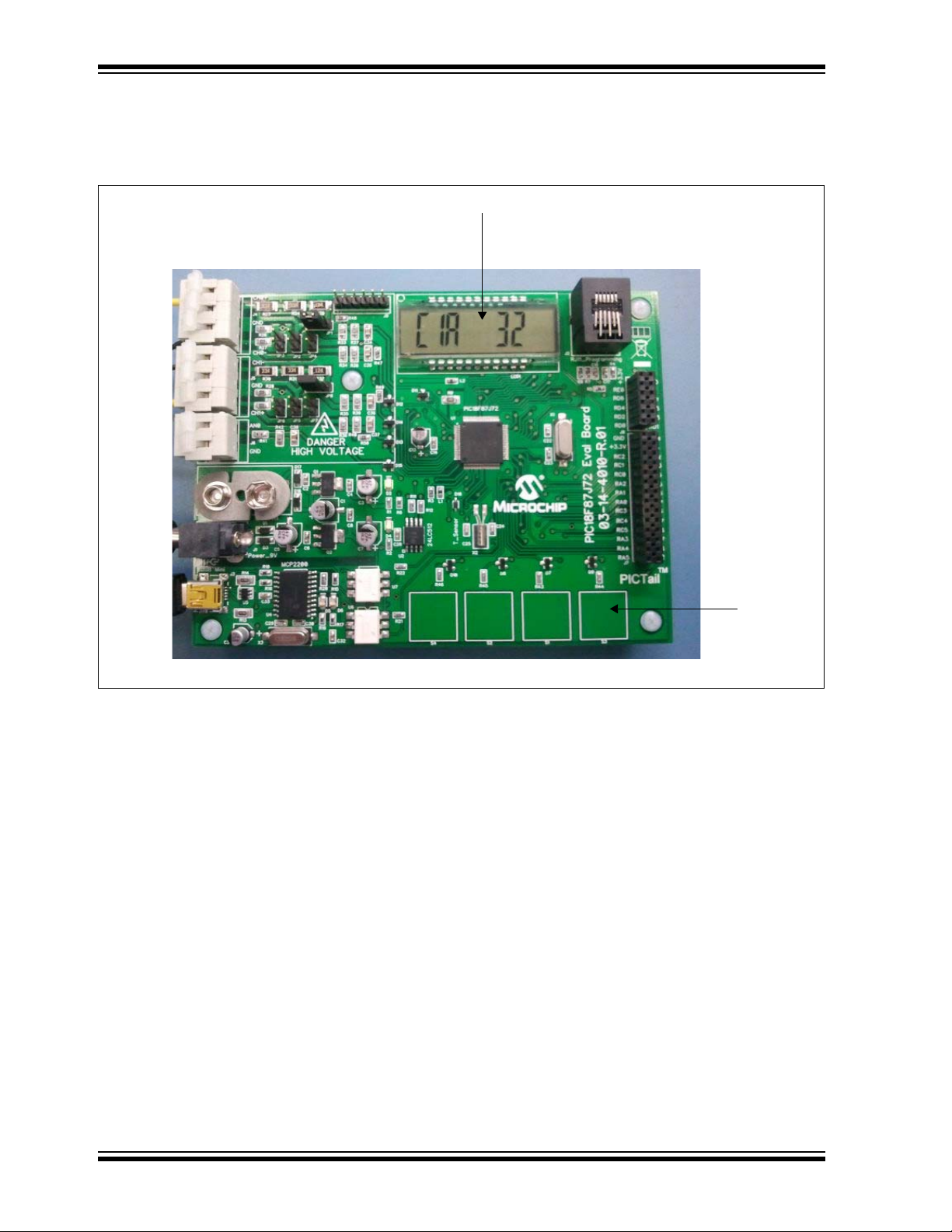
Figure 3-1 shows the PIC18F87J72 Evaluation Board with the 9V supply connected to
the input jack. The initial set up of the evaluation board involves connecting the supply
to the input jack of the board. This provides the required supply to the evaluation board.
Alternatively, the 9V battery can be connected to power the board. In addition, the USB
cable from the computer is connected to the mini USB connector on the board. This is
used for transmitting and receiving data to and from the board, to and from the GUI tool.
The input signal can be connected to connectors J4 and J5. If the microcontroller is
already programmed, then the program will start executing when the supply is turned
on.
PIC18F87J72 EVALUATION BOARD
USER’S GUIDE
Display showing the
configured OSR
Connect
I/P Signal
(J4 and J5)
9V Supply
Mini USB
RJ11
connector
Press S1 to
configure OSR
FIGURE 3-1: PIC18F87J72 Evaluation Board and OSR Configuration.
© 2011 Microchip Technology Inc. DS51990A-page 17
Page 18

PIC18F87J72 Evaluation Board User’s Guide
If the evaluation board is used in programmer mode, then the waveforms and the
response can be observed on the GUI. If the evaluation board is used in debugging
mode, using the MPLAB IDE, then the user can see the response on the Data Monitor
and Control Interface (DMCI) window.
For debugging, the Real ICE/ICD debugger and programmer is connected to the RJ11
connector. After the software is compiled and programmed to the PIC18F87J72 device,
the program can be executed. The LCD display on the board will indicate the time and
the waveforms that can be observed on the GUI window or DMCI. The LCD display on
the board will indicate the time. The various waveforms applied at the input can be
observed on the GUI or DMCI.
Various changes to the device configuration can be done using the touch sensitive keys
S1, S2, S3 and S4. The on-chip CTMU peripheral is used for all the touch-sensitive
keys.
Press the key S1, to change the Over Sampling Ratio (OSR) as shown in Figure 3-1.
There are four OSR configurations that can be created using S1. Each press of the key
S1 will change the configuration of the sigma delta ADC with OSR values from a value
of 256, 128, 64 and 32.
The time from the RTCC can also be displayed using the key S1 as shown in
Figure 3-2.
The RTCC date and time can be set using the following steps:
• Press the keys S2 and S4 simultaneously to enter into the RTCC date setting
mode. The date field on the LCD will start blinking.
• The date can be changed by pressing the key S4 for incrementing and S2 for
decrementing. The key S1 can be used to set the day, month and year fields.
• Press the keys S1 and S2 simultaneously, to enter into the RTCC time setting
mode. The time field on the LCD will start blinking.
• The time can be changed by pressing the key S4 for incrementing and S2 for
decrementing. The key S1 can be used to set the hour, minute and second fields.
By pressing the key S1 repeatedly, the OSR configurations will sequentially change
from 256 to 32 and then back to 256.
Display showing Time
Press S1 to
view time
FIGURE 3-2: Displaying Time and Date
DS51990A-page 18 © 2011 Microchip Technology Inc.
Page 19

PIC18F87J72 Evaluation Board Features
As shown in Figure 3-3, the S2 key is used for changing the internal PGA gain of the
first channel. The gains can be changed from 1 to 32 with each press of the key. When
pressing the S2 key repeatedly, the gain configurations of the Sigma Delta ADC will
sequentially change from 1, 2, 4, 8, 16, 32 and then back to 1.
Display showing channel gain
FIGURE 3-3: Configuring Internal PGA Gain for voltage channel.
Press S2 to
configure
voltage gain
© 2011 Microchip Technology Inc. DS51990A-page 19
Page 20
PIC18F87J72 Evaluation Board User’s Guide
Figure 3-4 shows the function of the S3 key, which is used to change the internal gain
of the second input channel. The gains can be changed from 1 to 32 with each press
of the key. When pressing the S3 key repeatedly, the gain configurations of the Sigma
Delta ADC will sequentially change from 1, 2, 4, 8, 16, 32 and then back to 1.
Display showing channel gain
FIGURE 3-4: Configuring Internal PGA Gain for Current Channel.
Press S3 to
configure
current gain
DS51990A-page 20 © 2011 Microchip Technology Inc.
Page 21

PIC18F87J72 Evaluation Board Features
Figure 3-5 shows the function of the S4 key, which is used to change the bit width of
the ADC conversion. Two configurations of the ADC bits are possible, either 16-bit or
24-bit. When the S4 key is pressed repeatedly, the bits toggle between 16 and 24-bit
width.
Display showing
ADC bit width
Press S4 to configure
current gain
FIGURE 3-5: Configuring the Number of Bits.
© 2011 Microchip Technology Inc. DS51990A-page 21
Page 22

PIC18F87J72 Evaluation Board User’s Guide
NOTES:
DS51990A-page 22 © 2011 Microchip Technology Inc.
Page 23

PIC18F87J72 EVALUATION BOARD
USER’S GUIDE
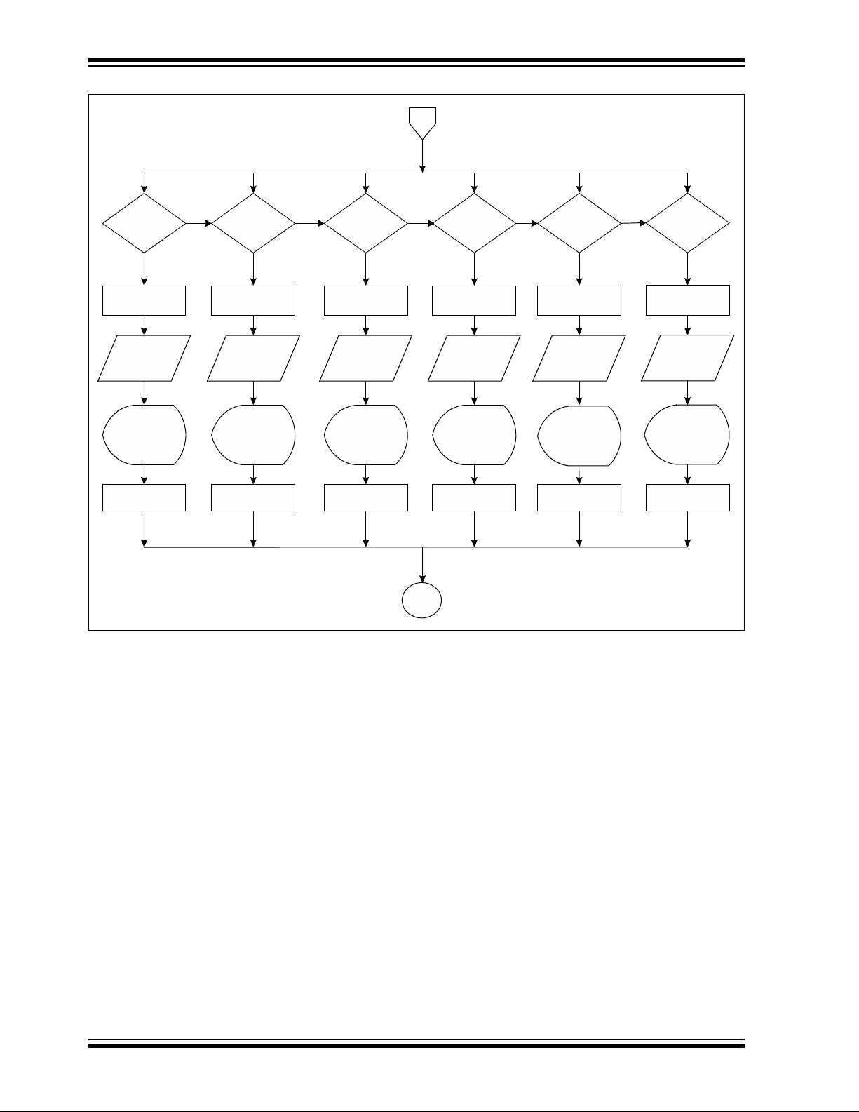
Chapter 4. PIC18F87J72 Evaluation Board Firmware Flowchart
4.1 INTRODUCTION
This chapter provides the flowcharts describing the functions and routines
implemented in the PIC18F87J72 Evaluation Board firmware.
Figures 4-1
• Main routine (see Figure 4-1)
• Touch Key press routines (see Figure 4-2)
• Time display routines (see Figure 4-2)
• OSR switching routines (see Figure 4-2)
• Channel CH0 Gain switching routines (see Figure 4-3)
• Channel CH1 Gain switching routines (see Figure 4-4)
• Bit width changing routines (see Figure 4-5)
• UART Transmit Interrupt routine (see Figure 4-6)
• UART Receive Interrupt routine (see Figure 4-6)
• INT0 Interrupt routine (see Figure 4-6)
– 4-6 show the flow of the following routines:
© 2011 Microchip Technology Inc. DS51990A-page 23
Page 24

PIC18F87J72 Evaluation Board User’s Guide
START
Initialize
Peripherals
SPI, UART
Configure ADC,
RTCC, CTMU
Charge CTMU
Pads of 4
Switches
SUM and
Average Voltage
Measure
Capacitor
Voltage
16
Idle
Calibrate for Pad
Sensitivity (if
required)
SW1
Press?
YES YES
1 2 3 4
OSR
or
Read Time
Switch
NO
SW2
Press?
CH0 Gain
Switch
Discharge CTMU
Pads of 4
Switches
Check for change
in Capacitance
NO
SW3
Press?
YES YES
CH1 Gain
Switch
NO
SW4
Press?
Bits
Switch
NO
High Priority
Interrupt
Service
Routine
5
YES
Interrupt
Request?
NO
Idle
FIGURE 4-1: Main Routine
DS51990A-page 24 © 2011 Microchip Technology Inc.
Page 25

PIC18F87J72 Evaluation Board Firmware Flowchart
1
osr_value = 0 osr_value = 1 osr_value = 2 osr_value = 3
YES
Disable Global
Interrupts
Set OSR
256, Write
Display
OSR = 256 on
LCD
Enable Global
Interrupts
NO
YES YES YES YES
Disable Global
Interrupts
Set OSR
128, Write
Display
OSR = 128 on
LCD
Enable Global
Interrupts
Disable Global
Interrupts
Set OSR
64, Write
Display
OSR = 64 on
LCD
Enable Global
Interrupts
Idle
Disable Global
Interrupts
Set OSR
32, Write
Display
OSR = 32 on
LCD
Enable Global
Interrupts
NONONO
osr_value = 4
Disable Global
Interrupts
Read
RTCC
Display TIME
HR:MIN:SEC
Enable Global
Interrupts
FIGURE 4-2: Key Press Routine to Configure OSR and Display Time.
© 2011 Microchip Technology Inc. DS51990A-page 25
Page 26
PIC18F87J72 Evaluation Board User’s Guide
2
gain1_value
= 0
YES
Disable Global
Interrupts
CH0
Gain=1,
Write
Display
GAIN = 1 on
LCD
Enable Global
Interrupts
NO
gain1_value
= 1
YES YES YES YES
Disable Global
Interrupts
CH0
Gain=2,
Write
Display
GAIN = 2 on
LCD
Enable Global
Interrupts
gain1_value
= 2
Disable Global
Interrupts
CH0
Gain=4,
Write
Display
GAIN = 4 on
LCD
Enable Global
Interrupts
Idle
gain1_value
= 3
Disable Global
Interrupts
CH0
Gain=8,
Write
Display
GAIN = 8 on
LCD
Enable Global
Interrupts
NONONO
gain1_value
= 4
Disable Global
Interrupts
CH0
Gain=16,
Write
Display
GAIN = 16 on
LCD
Enable Global
Interrupts
NO
gain1_value
= 5
YES
Disable Global
Interrupts
CH0
Gain=32,
Write
Display
GAIN = 32 on
LCD
Enable Global
Interrupts
FIGURE 4-3: Key Press Routine to Configur e Ga in of Channel CH0.
DS51990A-page 26 © 2011 Microchip Technology Inc.
Page 27

PIC18F87J72 Evaluation Board Firmware Flowchart
3
gain2_value
= 0
YES
Disable Global
Interrupts
CH1
Gain=1,
Write
Display
GAIN = 1 on
LCD
Enable Global
Interrupts
NO
gain2_value
= 1
YES YES YES YES
Disable Global
Interrupts
CH1
Gain=2,
Write
Display
GAIN = 2 on
LCD
Enable Global
Interrupts
gain2_value
= 2
Disable Global
Interrupts
CH1
Gain=4,
Write
Display
GAIN = 4 on
LCD
Enable Global
Interrupts
gain2_value
= 3
Disable Global
Interrupts
CH1
Gain=8,
Write
Display
GAIN = 8 on
LCD
Enable Global
Interrupts
Idle
NONONO
gain2_value
= 4
Disable Global
Interrupts
CH1
Gain=16,
Write
Display
GAIN = 16 on
LCD
Enable Global
Interrupts
NO
gain2_value
= 5
YES
Disable Global
Interrupts
CH1
Gain=32,
Write
Display
GAIN = 32 on
LCD
Enable Global
Interrupts
FIGURE 4-4: Key Press Routine to Configur e Ga in of Chann el CH1.
© 2011 Microchip Technology Inc. DS51990A-page 27
Page 28
PIC18F87J72 Evaluation Board User’s Guide
4
bit_width = 0 bit_width = 1
YES
Disable Global
Interrupts
Set Bits
16, Write
Display
BITS = 16 on
LCD
Enable Global
Interrupts
NO
YES
Disable Global
Interrupts
Set bits
24, Write
Display
BITS = 24 on
LCD
Enable Global
Interrupts
Idle
FIGURE 4-5: Key Press Routine to Configure Bit Width of Channel CH0 and CH1.
DS51990A-page 28 © 2011 Microchip Technology Inc.
Page 29

PIC18F87J72 Evaluation Board Firmware Flowchart
5
UART
TX Interrupt
Flag = 1?
Transmit
Data from
TXREG1
Disable UART TX
Interrupt
Enable INT0
Interrupt
Return From
Interrupt
UART
RX Interrupt
Flag = 1?
Receive
Data from
RCREG1
Process and Write
Data to TXREG1
Disable UART RX
Interrupt
Enable UART TX
Interrupt
INT0
Interrupt
Flag = 1?
Measure
CH0, CH1
Signals
through SPI
Store Data in
RAM for DMCI
or UART
Disable INT0
Interrupt
Enable UART RX
Interrupt
Return From
Interrupt
Return From
FIGURE 4-6: Interrupt Service Routine for UART and INT0 Interrupts.
Interrupt
© 2011 Microchip Technology Inc. DS51990A-page 29
Page 30

PIC18F87J72 Evaluation Board User’s Guide
NOTES:
DS51990A-page 30 © 2011 Microchip Technology Inc.
Page 31

PIC18F87J72 EVALUATION BOARD
USER’S GUIDE
Chapter 5. PIC18F87J72 Evaluation Board Lab Test Results
5.1 INTRODUCTION
This chapter provides the various laboratory test results obtained when using the
PIC18F87J72 Evaluation Board. This chapter also describes the use of the Data
Monitor and Control Interface (DMCI) window to plot the waveforms present on
Channel CH0 and CH1 of the evaluation board. Displaying waveforms on the DMCI
window can only be done when the user is working in Debugging mode. In Debugging
mode, the MPLAB IDE needs to be uploaded and the debugger connected to the RJ11
connector of the PIC18F87J72 Evaluation Board.
Figure 5-1 shows two graphs (i.e., Graph 1 and Graph 2). Graph 1 shows the waveform
created on Channel CH0 of the PIC18F87J72 Evaluation Board. Graph 2 shows the
waveform created on Channel CH1 of the PIC18F87J72 Evaluation Board. CH0 and
CH1 are both connected to the same signal of 300 mV. The internal PGA gain is chosen
to be 8 for CH0 and 1 for Channel CH1.
FIGURE 5-1: DMCI Waveforms for 300mV Waveform with CH0 Gain = 8, CH1 Gain = 1.
© 2011 Microchip Technology Inc. DS51990A-page 31
Page 32

PIC18F87J72 Evaluation Board User’s Guide
Figure 5-2 shows Graph 1 for CH0 and Graph 2 for CH1. The OSR for both CH0 and
CH1 are chosen to be 32 and the signal amplitude applied at the input is a very low
voltage sine wave signal of about 20 mV peak. The user can clearly observe the
distortion of the waveform with such a low OSR value.
FIGURE 5-2: DMCI Waveforms for 20mV Waveform with OSR = 32 on CH0 and CH1.
DS51990A-page 32 © 2011 Microchip Technology Inc.
Page 33

PIC18F87J72 Evaluation Board Lab Test Results
Figure 5-3 shows Graph 1 for CH0 and Graph 2 for CH1. The OSR for both CH0 and
CH1 are chosen to be 256 and the same signal is applied at the input with a very low
voltage sine wave signal of about 20 mV peak. Here, the sine wave shape is still
retained and the signal distortion is less when compared to Figure 5-2.
FIGURE 5-3: DMCI Waveforms for 20mV Waveform with OSR = 256 on CH0 and CH1.
© 2011 Microchip Technology Inc. DS51990A-page 33
Page 34

PIC18F87J72 Evaluation Board User’s Guide
Figure 5-4 shows Graph 1 for CH0 and Graph 2 for CH1. CH0 and CH1 are both
connected to the same signal of 300 mV. The internal PGA gain is chosen to be 1 for
CH0 and 32 for Channel CH1. The waveform on Graph 1 is intact, while the waveform
on Graph 2 is saturated at a value of 32768. This demonstrates the effect of saturation
when larger gains are used. This would distort the wave to a flat top waveform, and the
information related to the shape of the signal would be lost.
FIGURE 5-4: DMCI Waveforms for 300mV Waveform with CH0 Gain = 1, CH1 Gain = 32.
DS51990A-page 34 © 2011 Microchip Technology Inc.
Page 35

Chapter 6. PIC18F87J72 Evaluation Board GUI
6.1 INTRODUCTION
This chapter describes the Graphical User Interface used for the PIC18F87J72
Evaluation Board. Figure 6-1 indicates the various waveforms and the parameters that
can be displayed on the GUI. The signals can be viewed in their real-time state in Time
domain as well as in Frequency domain. UART is used for communication between the
GUI and the microcontroller. The baud rate used for communication is 38400. To use
the GUI, the following run-time engines must be installed:
• Visa441runtime
• LVRTE86std
PIC18F87J72 EVALUATION BOARD
USER’S GUIDE
Length
FIGURE 6-1: PIC18F87J72 Evaluation Board Graphical User Interface.
© 2011 Microchip Technology Inc. DS51990A-page 35
Page 36

PIC18F87J72 Evaluation Board User’s Guide
NOTES:
DS51990A-page 36 © 2011 Microchip Technology Inc.
Page 37

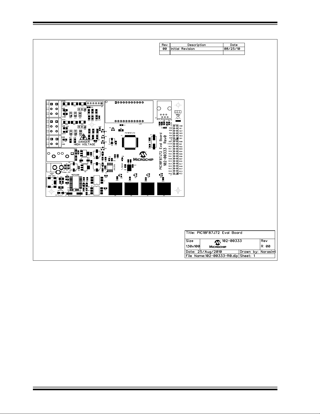
Appendix A. Schematics and Layouts
A.1 INTRODUCTION
This appendix contains the following schematics and layouts of the PIC18F87J72
Evaluation Board:
• Board – Schematic 1
• Board – Schematic 2
• Board – Schematic 3
• Board – Schematic 4
• Board – PCB Front Page
• Board – PCB Top Silk
• Board – PCB Top Layer
• Board – PCB Bottom Layer
• Board – PCB Bottom Silk
• Board – PCB L1 Ground
• Board – PCB L2 VDD
PIC18F87J72 EVALUATION BOARD
USER’S GUIDE
© 2011 Microchip Technology Inc. DS51990A-page 37
Page 38

PIC18F87J72 Evaluation Board User’s Guide
A.2 BOARD – SCHEMATIC 1
DS51990A-page 38 © 2011 Microchip Technology Inc.
Page 39

A.3 BOARD – SCHEMATIC 2
Schematics and Layouts
RG1* is Unused Pin
© 2011 Microchip Technology Inc. DS51990A-page 39
Page 40

PIC18F87J72 Evaluation Board User’s Guide
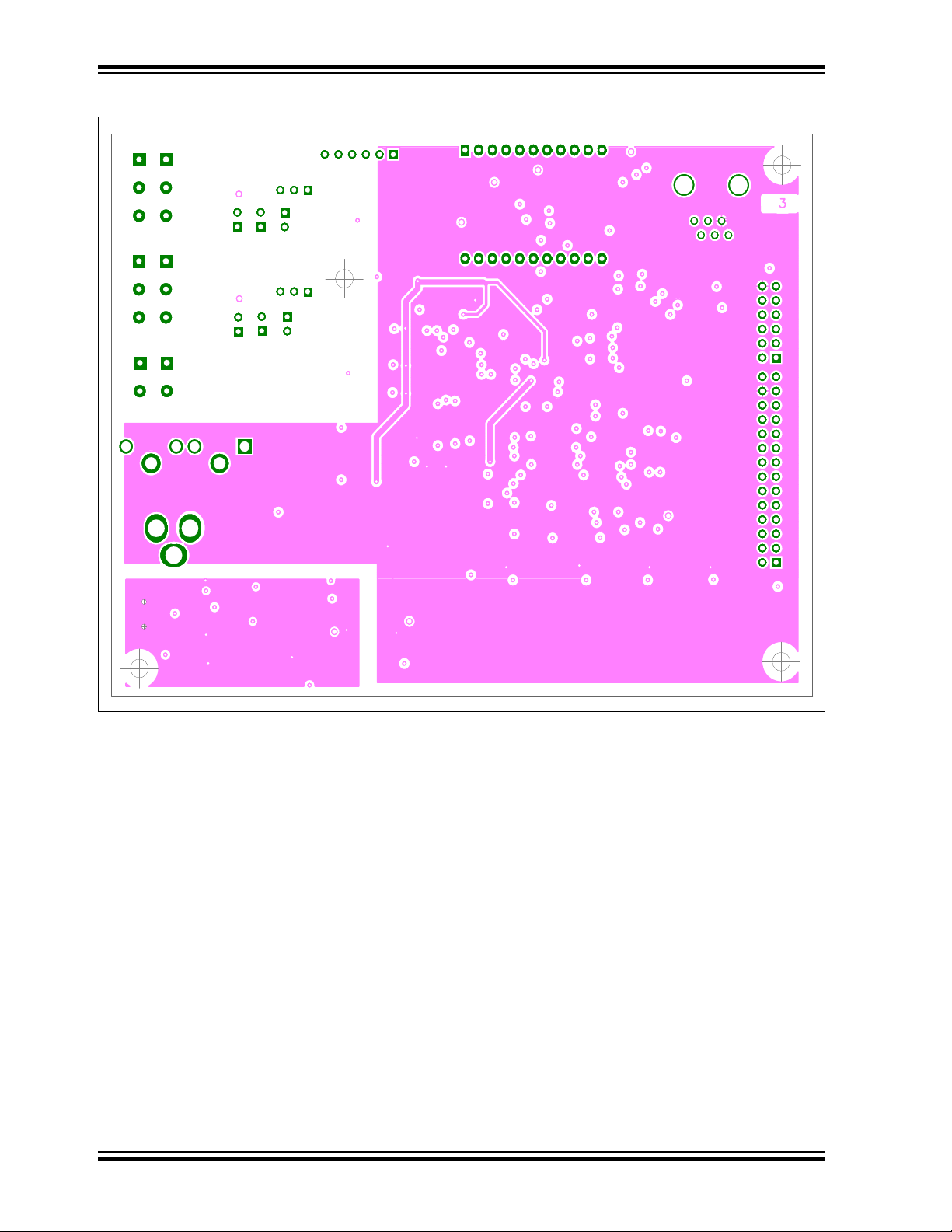
A.4 BOARD – SCHEMATIC 3
DS51990A-page 40 © 2011 Microchip Technology Inc.
Page 41

A.5 BOARD – SCHEMATIC 4
Schematics and Layouts
© 2011 Microchip Technology Inc. DS51990A-page 41
Page 42
PIC18F87J72 Evaluation Board User’s Guide
A.6 BOARD – PCB FRONT PAGE
PICTail
TM
DS51990A-page 42 © 2011 Microchip Technology Inc.
Page 43

A.7 BOARD – PCB TOP SILK
Schematics and Layouts
PICTail
TM
© 2011 Microchip Technology Inc. DS51990A-page 43
Page 44

PIC18F87J72 Evaluation Board User’s Guide
A.8 BOARD – PCB TOP LAYER
DS51990A-page 44 © 2011 Microchip Technology Inc.
Page 45

A.9 BOARD – PCB BOTTOM LAYER
Schematics and Layouts
© 2011 Microchip Technology Inc. DS51990A-page 45
Page 46

PIC18F87J72 Evaluation Board User’s Guide
A.10 BOARD – PCB BOTTOM SILK
DS51990A-page 46 © 2011 Microchip Technology Inc.
Page 47

A.11 BOARD – PCB L1 GROUND
Schematics and Layouts
© 2011 Microchip Technology Inc. DS51990A-page 47
Page 48
PIC18F87J72 Evaluation Board User’s Guide
A.12 BOARD – PCB L2 V
DD
DS51990A-page 48 © 2011 Microchip Technology Inc.
Page 49

PIC18F87J72 EVALUATION BOARD
USER’S GUIDE
Appendix B. Bill of Materials (BOM)
This chapter provides the Bill of Materials for all the components and devices used on
the PIC18F87J72 Evaluation Board.
TABLE B-1: BILL OF MATERIALS (BOM)
Qty Reference Description Manufacturer Part Number
1 BAT1 BATTERY IND ALKALINE 9 VOLT Energizer EN22
1 BAT1 CONN PC VERT 9V SNAP-ON Keystone 96B
4 C1, C3, C5, C7CAP 47UF 16V ELECT FP SMD Panasonic
®
ECG EEE-FPC470UAR
16 C2, C4, C6,
C8, C14,
C15, C16,
C17, C18,
C19, C20,
C21, C27,
C28, C32,
C33
5 C9, C10,
C11, C12,
C26
2 C13, C31 CAP 10UF 16V ELECT FP SMD Panasonic ECG EEE-FP1C100AR
4 C22, C23,
C29, C30
2 C24, C25 CAP CER 12PF 50V C0G 5% 0603 TDK Corporation C1608C0G1H120J
5 C34, C35,
C36, C37,
C38
4 D1, D3,
D16, D17
2 D2, D4 LED GREEN CLEAR 0805 SMD Lite-On Semi. LTST-C170GKT
2 D5, D6 LED YELLOW CLEAR 0805 SMD Lite-On Semi. LTST-C170YKT
9 D7, D8, D9,
D10, D11,
D12, D13,
D14, D15
1 D18 DIODE 75V 150MA SOD323F Fairchild Semi. 1N4148WS
1 J1 CONN POWERKJACK MINI R/A T/H Switchcraft RAPC722X
1 J2 CONN 6-6 MOD JACK Stewart Connector SS-7066-NF
1 J3 CONN USB RCPT MINI B 5PS R/A SMD JAE Electronics DX2R005HN2E700
2 J4, J5 TERMINAL BLOCK 5MM 3POS PCB On-Shore Tech. ED3101/3-WD
1 J6 TERMINAL BLOCK 5MM 2POS PCB On-Shore Tech. ED3101/2-WD
1 J7 CONN RECEPT 28POS .100 VERT DUAL TE Connectivity 1-234998-4
1 J8 CONN RECEPT 12POS .100 VERT DUAL 3M 960230-6202-AR
1 J9 CONN HEADER 6POS .100” STR TIN Molex 90120-0126
CAP CER .1UF 25V Y5V 0603 Murata
Electronics
CAP CER 47000PF 50V X7R 10% 0603 TDK Corporation C1608X7R1H473K
CAP CER 18PF 50V C0G 5% 0603 TDK Corporation C1608C0G1H180J
CAP CER 10000PF 50V 10% X7R 0805 Murata Electronics GRM216R71H103KA01D
DIODE SCHOTTKY 20V 500MA SOD123 Micro Commercial
Components
DIODE SWITCH 215MA 70V SOT-23 Comchip Tech. BAV99-G
®
GRM188F51E104ZAA01D
MBR0520-TP
© 2011 Microchip Technology Inc. DS51990A-page 49
Page 50

Bill of Materials (BOM)
TABLE B-1: BILL OF MATERIALS (BOM) (CONTINUED)
Qty Reference Description Manufacturer Part Number
2 JP1, JP8 CONN HEADER 3POS .100” STR TIN Molex 90120-0123
6JP2, JP3,
JP4, JP5,
JP6, JP7
2 L1, L2 FERRITE CHIP 120 OHM 2000MA 0603 Murata Electronics BLM18PG121SN1D
1 LCD1 Energy Meter LCD Display Deepkashi Display
1 PCB RoHS Compliant Bare PCB, PIC18F87J72
1 Q1 IC REG LDO 800MA 5.0V SOT-223 National Semi. LM1117MPX-5.0/NOPB
1 Q2 IC REG LDO 800MA 3.3V SOT-223 National Semi. LM1117MPX-3.3/NOPB
11 R1, R2, R5,
R11, R12,
R15, R16,
R17, R18,
R19, R21
1 R3 RES 0.0 OHM 1/10W 0603 SMD Stackpole Elec. RMCF 1/16 0 R
7 R4, R7, R8,
R47, R48,
R49, R50
1 R6 RES 10K OHM 1/10W 5% 0603 SMD Stackpole Elec. RMCF 1/16 10K 5% R
1 R9 RES 1.0 OHM 1/4W 5% 1206 SMD ROHM Semi. MCR18EZPJ1R0
2 R13, R14 RES 47.0 OHM 1/4W 1% 1206 SMD ROHM Semi. MCR18EZPF47R0
2 R20, R22 RES 470 OHM 1/10W 5% 0603 SMD Stackpole Elec. RMCF 1/16 470 5% R
4 R23, R24,
R30, R31
2 R25, R32 RES 120K OHM 1/2W 5% 2010 SMD ROHM Semi. MCR50JZHJ124
4 R26, R27,
R28, R29
10 R33, R34,
R35, R36,
R37, R38,
R39, R40,
R41, R42
4R43, R44,
R45, R46
1 U1 80-Pin, High-Performance Microcontrollers with
1 U2 512K I2C Serial EEPROM SOIC-8 Microchip Tech. Inc. 24LC512-I/SM
2 U3, U6 OPTOCOUPLER LOGIC OUT VDE 6-SMD Fairchild Semi. H11L1SR2VM
1 U4 USB 2.0 to UART protocol Converter with GPIO
1 U5 IC ESD PROTECTION LO CAP SOT23-6 STMicroelectronics USBLC6-2SC6
1 X1 CRYSTAL 10.000MHZ 18PF SMD ECS Ltd. ECS-100-18-5PX-TR
1 X2 CRYSTAL 32.768 KHZ 12.5PF CYL ECS Ltd. ECS-327-12.5-13X
1 X3 CRYSTAL 12.000MHZ 18PF SMD ECS Ltd. ECS-120-18-5PX-TR
CONN HEADER 2POS .100 VERT TIN Molex/Waldom
Electronics Corp.
Devices
Evaluation Board
RES 1K OHM 1/10W 5% 0603 SMD Stackpole Elec. RMCF 1/16 1K 5% R
RES 100 OHM 1/10W 5% 0603 SMD Stackpole Elec. RMCF 1/16 100 5% R
RES 330K OHM 1/2W 5% 2010 SMD ROHM Semi. MCR50JZHJ334
RES 47 OHM 1/8W .1% 0805 SMD Panasonic ECG ERA-6AEB470V
RES 1.0K OHM 1/8W .1% 0805 SMD SUSUMU Co. RG2012P-102-B-T
RESISTOR 1.0 OHM 1/10W 5% 0603 Panasonic ECG ERJ-3GEYJ1R0V
Microchip Tech. Inc. PIC18F87J72-I/PT
Dual-Channel AFE, LCD Driver and nanoWatt
Technology TQFP-80
Microchip
SSOP-20
Te c hn ol og y I n c.
22-03-2021
DP-093
104-00333
MCP2200-I/SO
© 2011 Microchip Technology Inc. DS51990A-page 50
Page 51

NOTES:
© 2011 Microchip Technology Inc. DS51990A-page 51
Page 52

Worldwide Sales and Service
AMERICAS
Corporate Office
2355 West Chandler Blvd.
Chandler, AZ 85224-6199
Tel: 480-792-7200
Fax: 480-792-7277
Technical Support:
http://www.microchip.com/
support
Web Address:
www.microchip.com
Atlanta
Duluth, GA
Tel: 678-957-9614
Fax: 678-957-1455
Boston
Westborough, MA
Tel: 774-760-0087
Fax: 774-760-0088
Chicago
Itasca, IL
Tel: 630-285-0071
Fax: 630-285-0075
Cleveland
Independence, OH
Tel: 216-447-0464
Fax: 216-447-0643
Dallas
Addison, TX
Tel: 972-818-7423
Fax: 972-818-2924
Detroit
Farmington Hills, MI
Tel: 248-538-2250
Fax: 248-538-2260
Indianapolis
Noblesville, IN
Tel: 317-773-8323
Fax: 317-773-5453
Los Angeles
Mission Viejo, CA
Tel: 949-462-9523
Fax: 949-462-9608
Santa Clara
Santa Clara, CA
Tel: 408-961-6444
Fax: 408-961-6445
Toronto
Mississauga, Ontario,
Canada
Tel: 905-673-0699
Fax: 905-673-6509
ASIA/PACIFIC
Asia Pacific Office
Suites 3707-14, 37th Floor
Tower 6, The Gateway
Harbour City, Kowloon
Hong Kong
Tel: 852-2401-1200
Fax: 852-2401-3431
Australia - Sydney
Tel: 61-2-9868-6733
Fax: 61-2-9868-6755
China - Beijing
Tel: 86-10-8569-7000
Fax: 86-10-8528-2104
China - Chengdu
Tel: 86-28-8665-5511
Fax: 86-28-8665-7889
China - Chongqing
Tel: 86-23-8980-9588
Fax: 86-23-8980-9500
China - Hangzhou
Tel: 86-571-2819-3180
Fax: 86-571-2819-3189
China - Hong Kong SAR
Tel: 852-2401-1200
Fax: 852-2401-3431
China - Nanjing
Tel: 86-25-8473-2460
Fax: 86-25-8473-2470
China - Qingdao
Tel: 86-532-8502-7355
Fax: 86-532-8502-7205
China - Shanghai
Tel: 86-21-5407-5533
Fax: 86-21-5407-5066
China - Shenyang
Tel: 86-24-2334-2829
Fax: 86-24-2334-2393
China - Shenzhen
Tel: 86-755-8203-2660
Fax: 86-755-8203-1760
China - Wuhan
Tel: 86-27-5980-5300
Fax: 86-27-5980-5118
China - Xian
Tel: 86-29-8833-7252
Fax: 86-29-8833-7256
China - Xiamen
Tel: 86-592-2388138
Fax: 86-592-2388130
China - Zhuhai
Tel: 86-756-3210040
Fax: 86-756-3210049
ASIA/PACIFIC
India - Bangalore
Tel: 91-80-3090-4444
Fax: 91-80-3090-4123
India - New Delhi
Tel: 91-11-4160-8631
Fax: 91-11-4160-8632
India - Pune
Tel: 91-20-2566-1512
Fax: 91-20-2566-1513
Japan - Yokohama
Tel: 81-45-471- 6166
Fax: 81-45-471-6122
Korea - Daegu
Tel: 82-53-744-4301
Fax: 82-53-744-4302
Korea - Seoul
Tel: 82-2-554-7200
Fax: 82-2-558-5932 or
82-2-558-5934
Malaysia - Kuala Lumpur
Tel: 60-3-6201-9857
Fax: 60-3-6201-9859
Malaysia - Penang
Tel: 60-4-227-8870
Fax: 60-4-227-4068
Philippines - Manila
Tel: 63-2-634-9065
Fax: 63-2-634-9069
Singapore
Tel: 65-6334-8870
Fax: 65-6334-8850
Taiwan - Hsin Chu
Tel: 886-3-6578-300
Fax: 886-3-6578-370
Taiwan - Kaohsiung
Tel: 886-7-213-7830
Fax: 886-7-330-9305
Taiwan - Taipei
Tel: 886-2-2500-6610
Fax: 886-2-2508-0102
Thailand - Bangkok
Tel: 66-2-694-1351
Fax: 66-2-694-1350
EUROPE
Austria - Wels
Tel: 43-7242-2244-39
Fax: 43-7242-2244-393
Denmark - Copenhagen
Tel: 45-4450-2828
Fax: 45-4485-2829
France - Paris
Tel: 33-1-69-53-63-20
Fax: 33-1-69-30-90-79
Germany - Munich
Tel: 49-89-627-144-0
Fax: 49-89-627-144-44
Italy - Milan
Tel: 39-0331-742611
Fax: 39-0331-466781
Netherlands - Drunen
Tel: 31-416-690399
Fax: 31-416-690340
Spain - Madrid
Tel: 34-91-708-08-90
Fax: 34-91-708-08-91
UK - Wokingham
Tel: 44-118-921-5869
Fax: 44-118-921-5820
05/02/11
DS51990A-page 52 © 2011 Microchip Technology Inc.
 Loading...