

Page 1

8-Bit Wireless Development Kit
User’s Guide
© 2011-2012 Microchip Technology Inc. Preliminary DS70654B
Page 2

Note the following details of the code protection feature on Microchip devices:
• Microchip products meet the specification contained in their particular Microchip Data Sheet.
• Microchip believes that its family of products is one of the most secure families of its kind on the market today, when used in the
intended manner and under normal conditions.
• There are dishonest and possibly illegal methods used to breach the code protection feature. All of these methods, to our
knowledge, require using the Microchip products in a manner outside the operating specifications contained in Microchip’s Data
Sheets. Most likely, the person doing so is engaged in theft of intellectual property.
• Microchip is willing to work with the customer who is concerned about the integrity of their code.
• Neither Microchip nor any other semiconductor manufacturer can guarantee the security of their code. Code protection does not
mean that we are guaranteeing the product as “unbreakable.”
Code protection is constantly evolving. We at Microchip are committed to continuously improving the code protection features of our
products. Attempts to break Microchip’s code protection feature may be a violation of the Digital Millennium Copyright Act. If such acts
allow unauthorized access to your software or other copyrighted work, you may have a right to sue for relief under that Act.
Information contained in this publication regarding device
applications and the like is provided only for your convenience
and may be superseded by updates. It is your responsibility to
ensure that your application meets with your specifications.
MICROCHIP MAKES NO REPRESENTATIONS OR
WARRANTIES OF ANY KIND WHETHER EXPRESS OR
IMPLIED, WRITTEN OR ORAL, STATUTORY OR
OTHERWISE, RELATED TO THE INFORMATION,
INCLUDING BUT NOT LIMITED TO ITS CONDITION,
QUALITY, PERFORMANCE, MERCHANTABILITY OR
FITNESS FOR PURPOSE. Microchip disclaims all liability
arising from this information and its use. Use of Microchip
devices in life support and/or safety applications is entirely at
the buyer’s risk, and the buyer agrees to defend, indemnify and
hold harmless Microchip from any and all damages, claims,
suits, or expenses resulting from such use. No licenses are
conveyed, implicitly or otherwise, under any Microchip
intellectual property rights.
Trademarks
The Microchip name and logo, the Microchip logo, dsPIC,
K
EELOQ, KEELOQ logo, MPLAB, PIC, PICmicro, PICSTART,
32
PIC
logo, rfPIC and UNI/O are registered trademarks of
Microchip Technology Incorporated in the U.S.A. and other
countries.
FilterLab, Hampshire, HI-TECH C, Linear Active Thermistor,
MXDEV, MXLAB, SEEVAL and The Embedded Control
Solutions Company are registered trademarks of Microchip
Technology Incorporated in the U.S.A.
Analog-for-the-Digital Age, Application Maestro, chipKIT,
chipKIT logo, CodeGuard, dsPICDEM, dsPICDEM.net,
dsPICworks, dsSPEAK, ECAN, ECONOMONITOR,
FanSense, HI-TIDE, In-Circuit Serial Programming, ICSP,
Mindi, MiWi, MPASM, MPLAB Certified logo, MPLIB,
MPLINK, mTouch, Omniscient Code Generation, PICC,
PICC-18, PICDEM, PICDEM.net, PICkit, PICtail, REAL ICE,
rfLAB, Select Mode, Total Endurance, TSHARC,
UniWinDriver, WiperLock and ZENA are trademarks of
Microchip Technology Incorporated in the U.S.A. and other
countries.
SQTP is a service mark of Microchip Technology Incorporated
in the U.S.A.
All other trademarks mentioned herein are property of their
respective companies.
© 2011-2012, Microchip Technology Incorporated, Printed in
the U.S.A., All Rights Reserved.
Printed on recycled paper.
ISBN: 978-1-61341-991-5
Microchip received ISO/TS-16949:2009 certification for its worldwide
headquarters, design and wafer fabrication facilities in Chandler and
T empe, Arizona; Gresham, Oregon and design centers in California
and India. The Company’s quality system processes and procedures
are for its PIC
devices, Serial EEPROMs, microperipherals, nonvolatile memo ry and
analog products. In addition, Microchip’s quality system for the desig n
and manufacture of development systems is ISO 9001:2000 certified.
®
MCUs and dsPIC® DSCs, KEELOQ
®
code hopping
DS70654B-page 2 Preliminary © 2011-2012 Microchip Technology Inc.
Page 3

8-BIT WIRELESS
DEVELOPMENT KIT
USER ’S GUIDE
Table of Contents
Preface ...........................................................................................................................5
Overview ........................................................................................................................9
Introduction ........................................................................................................... 9
8-Bit Wireless Development Kit Contents ............................................................ 9
Wireless Daughter Boards ...................................................................................9
8-Bit Wireless Development Kit ..........................................................................10
PIC18 Wireless Development Board .........................................................................11
Board Layout and Features ................................................................................11
Getting Started ............................................................................................................15
Introduction ......................................................................................................... 15
Hardware Requirements ....................................................................................15
Demo Setup .......................................................................................................15
Pre-programmed Tutorial Operation ..................................................................16
Additional Tutorials ....................................................................................................21
Introduction ......................................................................................................... 21
Extended 8-bit WDK Demo with Hyper-terminal Program .................................21
Network Freezer .................................................................................................23
Reduced Function Device (RFD) Demonstrating Sleep Capability .................... 25
Chat Window Demo ........................................................................................... 27
Ping-Pong Demo ................................................................................................ 29
8-bit Wireless Development Kit with Additional Nodes .......................................32
Introduction ......................................................................................................... 33
PIC18 Wireless Development Board Schematic ................................................ 33
PIC18 Wireless Development Board PCB Layout ..............................................36
PIC18 Wireless Development Board Bill of Materials ........................................ 38
Worldwide Sales and Service ....................................................................................41
© 2011-2012 Microchip Technology Inc. Preliminary DS70654B-page 3
Page 4

8-Bit Wireless Development Kit User’s Guide
NOTES:
DS70654B-page 4 Preliminary © 2011-2012 Microchip Technology Inc.
Page 5

8-BIT WIRELESS
DEVELOPMENT KIT
USER ’S GUIDE
Preface
NOTICE TO CUSTOMERS
All documentation becomes dated, and this manual is no exception. Microchip tools and
documentation are constantly evolving to meet customer needs, so some actual dialogs
and/or tool descriptions may differ from those in this document. Please refer to our web site
(www.microchip.com) to obtain the latest documentation available.
Documents are identified with a “DS” number. This number is located on the bottom of each
page, in front of the page number. The numbering convention for the DS number is
“DSXXXXXA”, where “XXXXX” is the document number and “A” is the revision level of the
document.
For the most up-to-date information on development tools, see the MPLAB® IDE on-line help.
Select the Help menu, and then Topics to open a list of available on-line help files.
INTRODUCTION
This chapter contains general information that will be useful to know before using the
8-bit Wireless Development Kit User’s Guide. Items discussed in this chapter include:
• Document Layout
• Conventions Used in this Guide
• Warranty Registration
• Recommended Reading
• The Microchip Web Site
• Development Systems Customer Change Notification Service
• Customer Support
DOCUMENT LAYOUT
This document describes how to use the 8-Bit Wireles s Deve lo pm e nt kit to evalu a te
and experiment with Microchip wireless solutions. The manual layout is as follows:
• Chapter 1. “Overview”: This chapter describes the 8-bit Wireless Development
Kit and how it works.
• Chapter 2. “PIC18 Wireless Development Board”: This chapter details the
hardware information of the PIC18 Wireless Development Board.
• Chapter 3. “Getting Started”: This chapter describes what you ne ed to kn ow to
start using the 8-bit Wireless Development Kit.
• Chapter 4. “Additional Tutorials”: This chapter provides ad dit ion a l tu to rial pro -
grams that demonstrate the additional features of 8-bit Wireless Development Kit.
• Appendix A. “PIC18 Wireless Development Board Schematic”: This appendix
provides the PCB layout, BOM and PIC18 Wireless Development Board
schematics.
© 2011-2012 Microchip Technology Inc. Preliminary DS70654B-page 5
Page 6
8-Bit Wireless Development Kit User’s Guide
CONVENTIONS USED IN THIS GUIDE
This manual uses the following documentation conventions:
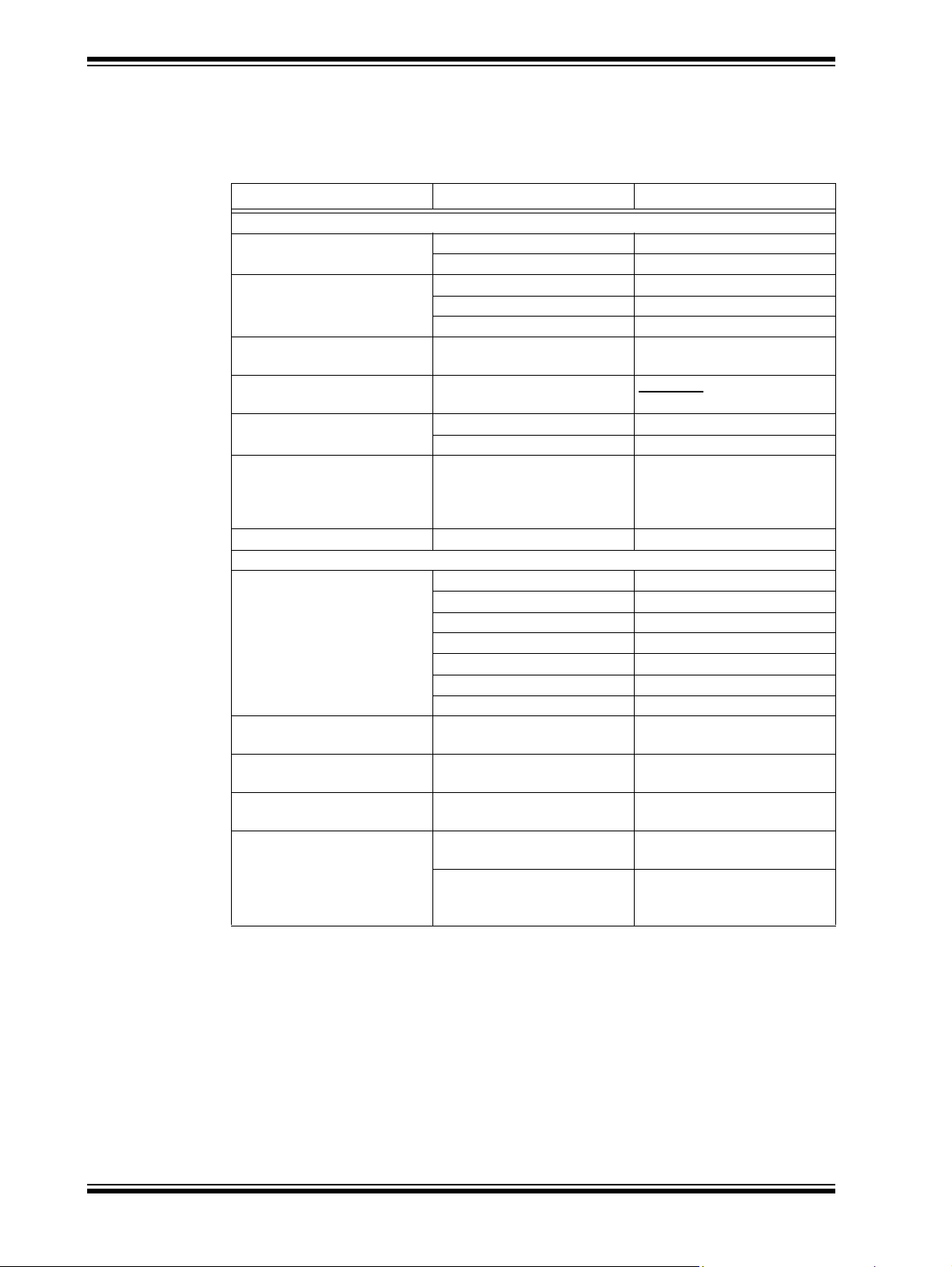
DOCUMENTATION CONVENTIONS
Description Represents Examples
sArial font:
Italic characters Referenced books MPLAB® IDE User’s Guide
Emphasized text ...is the only compiler...
Initial caps A window the Output window
A dialog the Settings dialog
A menu selection select Enable Programmer
Quotes A field name in a window or
dialog
Underlined, italic text with
right angle bracket
Bold characters A dialog button Click OK
N‘Rnnnn A number in verilog format,
Text in angle brackets < > A key on the keyboard Press <Enter>, <F1>
Courier New font:
Plain Courier New Sample source code #define START
Italic Courier New A variable argument file.o, where file can be
Square brackets [] Optional arguments mcc18 [options] file
Curly brackets and pipe
character: {|}
Ellipses... Replaces repeated text var_name [,
A menu path File>Save
A tab Click the Power tab
where N is the total number of
digits, R is the radix and n is a
digit.
Filenames autoexec.bat
File paths c:\mcc18\h
Keywords _asm, _endasm, static
Command-line options -Opa+, -Opa-
Bit values 0, 1
Constants 0xFF, ‘A’
Choice of mutually exclusive
arguments; an OR selection
Represents code supplied by
user
“Save project before build”
4‘b0010, 2‘hF1
any valid filename
[options]
errorlevel {0|1}
var_name...]
void main (void)
{...
}
DS70654B-page 6 Preliminary © 2011-2012 Microchip Technology Inc.
Page 7

WARRANTY REGISTRATION
Please complete the enclosed Warran ty Registration Card and mail it promptly.
Sending in the Warranty Registration Card entitles users to receive new product
updates. Interim software releases are available at the Microchip web site.
RECOMMENDED READING
This user’s guide describes how to use 8-bit Wireless Development Kit User’s Guide.
Other useful documents are listed below. The following Microchip documents are
available and recommended as supple me n tal refere nce re sou r ces .
Readme Files
For the latest information on using other tools, read the tool-specific Readme files in
the Readmes subdirectory of the MPLAB IDE installation directory. The Readme files
contain update information and known issues that may not be included in this user’s
guide.
THE MICROCHIP WEB SITE
Microchip provides online support via our web site at www.microchip.com. This web
site is used as a means to make files and information easily available to customers.
Accessible by using your favorite Internet browser , the web site contains the following
information:
• Product Support – Data sheets and errata, application notes and sample
programs, design resources, user’s guides and hardware support documents,
latest software releases and archived software
• General Technical Support – Frequently Asked Questions (FAQs), technical
support requests, online discussion groups, Microchip consultant program
member listing
• Business of Microchip – Product selector and ordering guides, latest Microchip
press releases, listing of seminars and events, listings of Microchip sales offices,
distributors and factory representatives
Preface
© 2011-2012 Microchip Technology Inc. Preliminary DS70654B-page 7
Page 8

8-Bit Wireless Development Kit User’s Guide
DEVELOPMENT SYSTEMS CUSTOMER CHANGE NOTIFICATION SERVICE
Microchip’s customer notification service helps keep customers current on Microchip
products. Subscribers will receive email notification whenever there are changes,
updates, revisions or errata related to a spec ified product family or development tool of
interest.
To register, access the Microchip web site at www.microchip.com, click on Customer
Change Notification and follow the registration instructions.
The Development Systems product group categories are:
• Compilers – The latest information on Microchip C compilers a nd other language
tools. These include the MPLAB C18 and MPLAB C30 C compilers; MPASM™
and MPLAB ASM30 assemblers; MPLINK™ and MPLAB LINK30 object linkers;
and MPLIB™ and MPLAB LIB30 object librarians.
• Emulators – The latest information on Microchip in-circuit emulators.This
includes the MPLAB ICE 2000 and MPLAB ICE 4000.
• In-Circuit Debuggers – The latest information on the Microchip in-circuit
debugger , MPLAB ICD 2.
• MPLAB® IDE – The latest information on Microchip MPLAB IDE, the Windows®
Integrated Development Environment for development systems tools. This list is
focused on the MPLAB IDE, MPLAB SIM simulator, MPLAB IDE Project Manager
and general editing and debugging features.
• Programmers – The latest information on Microchip programmers. These include
the MPLAB PM3 and PRO MATE
Plus and PICkit™ 1 development programmers.
®
II device programmers and the PICSTART®
CUSTOMER SUPPORT
Users of Microchip products can receive assistance through several channels:
• Distributor or Representative
• Local Sales Office
• Field Application Engineer (FAE)
• Technical Support
Customers should contact their distributor, representative or field application engineer
(FAE) for support. Local sa les of fices ar e also available to help cu stomers. A listing of
sales offices and locations is included in the back of this document.
Technical support is available through the web site at: http://support.microchip.com
DS70654B-page 8 Preliminary © 2011-2012 Microchip Technology Inc.
Page 9

DOCUMENT REVISION HISTORY
Revision A (March 2011)
This is the initial release of the document.
Revision B (January 2012)
This revision includes the following updates:
• Added MRF89XAM8A868 MHz PICtail/PICtail Plus Daughter Boards or
MRF89XAM9A915 MHz PICtail/PICtail Plus Daughter Boards in 1.3 “Wireless Daughter
Boards”
• Added rows, MRF24J40MC and MRF89XAM9A PICtail/PICtail Plus Daughter Board, in
Table 1-1: “Compatible PICtail™ Daughter Boards”
• Added a new bullet in 3.3 “Demo Setup”, 4.2.1 “Set up”, 4.3.1 “Setup”,
4.5.1 “Setup”, 4.6.1 “Set up”
• Updated 4.3 “Network Freezer”
• Replaced all instances of MRF24J40MA Daughter Boards with Radio Daughe r
Boards
Preface
© 2011-2012 Microchip Technology Inc. Preliminary DS70654B-page 9
Page 10

8-Bit Wireless Development Kit User’s Guide
DS70654B-page 10 Preliminary © 2011-2012 Microchip Technology Inc.
Page 11
DEVELOPMENT KIT
Chapter 1. Overview
1.1 INTRODUCTION
This chapter introduces the 8-Bit Wireless Development Kit features and its
requirements.
The topics discussed in this chapter include:
• 8-Bit Wireless Development Kit Contents
• Wireless Daughter Boards
• 8-Bit Wireless Development Kit
1.2 8-BIT WIRELESS DEVELOPMENT KIT CONTENTS
The 8-Bit Wireless Development Kit contains the following items:
• Two PIC18 Wireless Development Boards with PIC18F46J50 XLP Microcontroller
• Two PICtail™/PICtail Plus Daughter Boards (See Table 1-1)
•Two LCD Serial Accessory Boards
• Two RS232 Serial Accessory Boards
• Two USB A to Mini-B 1 meter Cables
• Two RS232 Serial Cables
8-BIT WIRELESS
USER ’S GUIDE
1.3 WIRELESS DAUGHTER BOARDS
The 8-Bit Wireless Development Kit, includes either MRF24J40MA 2.4 GHz IEEE
802.15.4 complaint PICtail/PICtail Plus Daughter Boards or MRF89XAM8A 868 MHz
PICtail/PICtail Plus Daughter Boards or MRF89XAM9A 915 MHz PICtail/PICtail Plus
Daughter Boards. The PIC18 Wireless Development Board is compatible with many
other wireless PICtail daughter Boards.
PICtail daughter boards that are compatible with the PIC18 Wireless Development
Board.
TABLE 1-1: COMPATIBLE PICtail™ DAUGHTER BOARDS
Description Part Number
MRF24J40MA PICtail/PICtail Plus Daughter Board AC164134-1
MRF24J40MB PICtail/PICtail Plus Daughter Board AC164134-2
MRF24J40MC Pictail/PICtail Plus Daughter Board AC164134-3
MRF49XA PICtail Plus Daughter Board (433.92 MHz) AC164137-1
MRF49XA PICtail Plus Daughter Board (868/915 MHz) AC164137-2
MRF89XAM8A PICtail/PICtail Plus Daughter Board (868 MHz) AC164138-1
MRF89XAM9A PICtail/PICtail Plus Daughter Board (915 MHz) AC164138-2
Table 1-1 lists the part number of the wireless
© 2011-2012 Microchip Technology Inc. Preliminary DS70654B-page 9
Page 12

8-Bit Wireless Development Kit User’s Guide
The PIC18 Wireless Development Board provides PICtail connectivity, which is
compatible with the existing and future radio and sensor daughter boards from
Microchip. For more information on compatibility, refer to the Microchip website
http://www.microchip.com/wireless
Note: Individual Wireless PICtail Daughter Boards require .hex files for the
specific RF transceiver. For more information, refer to the 8-Bit Wireless
Development Kit product web page at http://www.microchip.com/wireless.
1.4 8-BIT WIRELESS DEVELOPMENT KIT
The Wireless Development Kit allows developers to evaluate and experiment with
sub-GHz and 2.4 GHz RF solutions from Microchip. The Wireless Development Kit
provides two RF hardware nodes which can be used to create a simple two-node
wireless network. More nodes can be added by purchasing 8-Bit Wireless
Development Kit or individual components.
The 8-Bit Wireless Development Kit is pre-programmed with a wireless demo prog ram
that allows multiple operational configurations to be tested without writing any firmware.
For more information on how to operate the pre-programmed demo program and how
to develop other applications, see
customer to evaluate Microch ip’s proprietary wireless stacks. The Microchip wireless
stacks and additional application demo source codes can be downloaded from the
Microchip web site
The PIC18 Wireless Development Board provides all the necessary components
required to build an extreme low-power wireless sensor application. The Serial
Accessory Port can interface external sensors or modules, like LCD Serial Accessory
Board or RS232 Serial Accessory Board. The platform provides USB connectivity and
supports different XLP microcontroller options.
http://www.microchip.com/wireless.
Chapter 3. “Getting Started”. It also enables
DS70654B-page 10 Preliminary © 2011-2012 Microchip Technology Inc.
Page 13
Chapter 2. PIC18 Wireless Development Board
2.1 BOARD LAYOUT AND FEATURES
This chapter describes the PIC18 Wireless Development Board hardware. It also
features the components shown in
FIGURE 2-1: PIC18 WIRELESS DEVELOPMENT BOARD
Figure 2-1.
8-BIT WIRELESS
DEVELOPMENT KIT
USER ’S GUIDE
© 2011-2012 Microchip Technology Inc. Preliminary DS70654B-page 11
Page 14

8-Bit Wireless Development Kit User’s Guide
The PIC18 Wireless Development Board supports the XLP microcontroller options
such as PIC18F46J11, PIC18F46J50, PIC18F46K20 and PIC18LF45K22.
The default microcontroller option is PIC18F46J50. Different microcontroller options
require different components to populate on the PIC18 Wireless Development Board.
Note 1: Missing components on the PIC18 Wireless Development Board does
not indicate a defect. Population of these missing components depend on
the Microcontroller being used. For more information about using
different Microcontrollers, see the Section A.2 “PIC18 Wireless
Development Board Schematic”.
2: Take pre cautionary measure while changing the microcon troller option as
improper tools or poor handling could harm the copper tracks on the
surface of the Board, it might destroy it.
The following main blocks are defined on the Board:
• Serial Accessory Port
• USB Interface Port
• PICtail Port
• Push Buttons
• Onboard Temperature Sensor
• Onboard Serial EEPROM
• Debug LEDs
• Power Supply
2.1.1 Serial Accessory Port
Serial Accessory Port provides a simple serial interface for the external modules.
These modules may be either external sensor or accessory board. For more
information about existing accessory boards refer to the
http://www.microchip.com or
“LCD Serial Accessory Board User’s Guide” (DS70650) or “RS232 Serial Accessory
Board User’s Guide” (DS70649).
The following interfaces are supported by the Serial Accessory Port:
• 3 or 4 wire SPI
•I2C™
• USART
These interfaces are selected by the software without modifying the hardware. User
should be attentive when different interfaces use the same hardware or sh are the same
port pins of the microcontroller. For more information on the port pin assignment, see
Figure A-1.
2.1.2 USB Interface Port
The PIC18F46J50 microcontroller provides USB v2.0 compliant full-speed Universal
Serial Bus (USB) interface, which helps suppling power to the PIC18 Wireless
Development Board. The relevant USB components are included with the
PIC18F46J50 microcontroller option.
DS70654B-page 12 Preliminary © 2011-2012 Microchip Technology Inc.
Page 15

PIC18 Wireless Development Board
//Initialize RB2
TRISBbits.TRISB2 = 1; // RB2 is an input
ANCON1 |= 0x01; // RB2 is a digital pin
/*
User code
*/
//Evaluating RB2
INTCON2bits.RBPU = 0; // PortB pull ups are enabled
if (PORBbits.RB2 == 0) // RB2 is pushed
{
/*
RB2 PB code...
*/
}
INTCON2bits.RBPU = 1; // PortB pull ups are disabled
2.1.3 PICtail Port
PICtail Port is a 28-pin interface port that supports Microchip’s RF based daughter
cards. PICtail Port provides the following interfaces to the daughter cards:
• Power supply
• SPI interface
• Interrupt request lines
Note: User must be careful about the PICtail port pins that share different
functions of the board. The user needs to check the schematics before
assigning functions for any port pins.
2.1.4 Push Buttons
PIC18 Wireless Development board contains two push buttons, RB0 and RB2. These
buttons are assigned to the individual interrupt lines of the microcontroller and are not
driven by external pull-up circuitry to save power consumption. The user software must
enable the Port B pull-ups of the microcontroller before evaluating the button state.
Example 2-1 illustrates a possible solution to evaluate the state of RB2.
EXAMPLE 2-1: CODE EXAMPLE FOR EVALUATING THE STATE OF RB2
2.1.5 Onboard Temperature Sensor
The temperature sensor used is the Microchip’s MC9700A, which is a low-power Linear
Active Thermistor™ IC. To minimize power consumption, the sensor is powered from
a port pin. After powering up, the sensor output can be measured after a minute. The
internal AD converter of the microcontroller is used to measure the temperature value.
© 2011-2012 Microchip Technology Inc. Preliminary DS70654B-page 13
2.1.6 Onboard Serial EEPROM
The Onboard Serial EEPROM is a low-power, Microchip’s 25LC256 256K SPI Bus
Serial EEPROM, which shares the SPI interface with the PICtail port. But Onboard
Serial EEPROM has its own active low chip select line connected to the RD5 port pin.
2.1.7 Debug LEDs
The PIC18 Wireless Development Board contains three LEDs for debug purposes. To
conserve battery power , LEDs power can be disconnected by removing the JP20 1 and
LED power jumper .
Page 16

8-Bit Wireless Development Kit User’s Guide
2.1.8 Power Supply
The board can be powered from any one of these sources:
• 2xAA onboard battery pack is available at the bottom of the PIC18 Wireless
Development Board
• USB port
• External 9-16V charger power supply through the standard coaxial power
connector
• External 3.0-3.6V power source through test points TP301 and TP302
USB Port and external coaxial port power are stabilized by MCP1703, 250 mA, 3.3V,
low quiescent current LDO regulator. The battery operated applications that do not
require LDO can be disconnected by removing the JP301, Regulator Disconnect
jumper.
Note: The 9V wall adapter is not included in the kit. A 9V wall adapter may be
ordered from
wall adapter is AC162039.
2.1.8.1 CURRENT CONSUMPTION MEASUREMENT
ThePIC18 Wireless Development Board contains two jumpers, JP302 and JP303, to
measure the current consumption of the kit. These jumpers can measure current
consumption of the entire kit without disturbin g it.
Measuring the operational current:
1. Ensure that either JP302 or JP303, has one jumper connected to it. Only one
jumper is required.
2. Connect the current meter to the jumper that is empty. Because the jumpers are
electrically parallel, it can be either JP302 or JP303.
3. Set the current measure range of the current meter above 250 mA.
4. Remove the jumper.
http://www.microchipdirect.com/ . The part number of the 9V
Note: Some current meters set the measuring range automatically, which can
cause interruptions in the power line while changing the range. If
interruption in the power line occurs, use manual range settings.
DS70654B-page 14 Preliminary © 2011-2012 Microchip Technology Inc.
Page 17

3.1 INTRODUCTION
This chapter provides a tutorial to familiarize users with the 8-bit Wireless Development
Kit. It also explains how to run the pre-programmed demo. The source code for the
demo is available along with the MiWi
MiWi stack, by default the file is saved at the following location
C:\Microchip Solutions\MiWi DE Demo\8-bit Wireless Development Kit –
(Transciver)\8-bit WDK Demo
The demo programs use the MiWi Development Environment. For more information
about MiWi, refer to
Note: To run the demo using the PIC18 Wireless out of the box demo boards, the
The following topics are discussed in this chapter:
• Hardware Requirements
•Demo Setup
• Pre-programmed Tutorial Operation
8-BIT WIRELESS
DEVELOPMENT KIT
USER ’S GUIDE
Chapter 3. Getting Started
TM
stack. After unzipping the latest version of the
.
www.microchip.com/MiWi.
user need not re-program them. Otherwise, the user needs to program this
with the 8-bit WDK
Demo.hex file.
3.2 HARDWARE REQUIREMENTS
The following hardwares are required to run the pre-programmed demo application:
• Two pre-programmed PIC18 Wireless Development Boards
• Two Radio Daughter Boards
•Two LCD Serial Accessory Boards
• Four fresh AA batteries or a two 9V external power supply or two USB cables
3.3 DEMO SETUP
This section demonstrates how to create a two node MiWi Wireless Network. Create a
network using the two push buttons (RB0 and RB2) available on the PIC18 Wireless
Development board (RB0 to create the network and RB2 to join the network). After
setting up the network the nodes in the network read the temperature sensor
(MCP9700A) and broadcast this information over the network.
Follow these steps to set up the 8-bit WDK demo:
1. Connect the LCD Serial Accessory board J1 port to the J101 connector on the
PIC18 Wireless Development Board (See
2. Plug in the Radio PICtail Daughter board at slot J201 on the PIC18 Wireless
Development Board.
3. To power using AA batteries, remove the jumper at JP301 (Regulator
Disconnect). To power through 9V external power supply or USB, ensure JP301
is connected (jumper installed).
4. Insert a jumper at JP201 (LED power) on the PIC18 Wireless Development Board.
Figure 3-1).
© 2011-2012 Microchip Technology Inc. Preliminary DS70654B-page 15
Page 18

8-Bit Wireless Development Kit User’s Guide
5. Ensure that the jumper is disconnected at JP1 position on the LCD Serial
Accessory Board. This ensures that the LCD Seria l Accessory Board is used in
2
I
C mode and not in SPI mode. The 8-bit WDK Demo program uses the LCD
Serial Accessory board in I
6. Wireless demo board can be powered using any of these options:
• Two AA Batteries
• 9V External Power Supply
• USB port
• External 3.0-3.6V power source through test points TP301and TP302
7. Insert a jumper at either JP302 or JP303 (Current Measure) on the PIC18
Wireless Development Board.
FIGURE 3-1: PIC18 WIRELESS DEVELOPMENT BOARD CONNECTED TO LCD SERIAL
ACCESSORY BOARD
AND MRF24J40MA PICTAIL DAUGHTER BOARD
2
C mode.
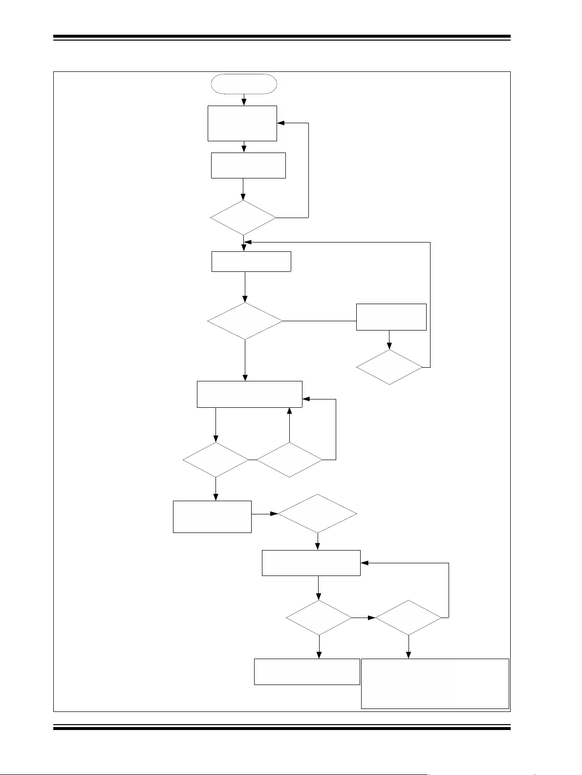
3.4 PRE-PROGRAMMED TUTORIAL OPERATION
The pre-programmed demo is used to demonstrate the basic concepts of the MiWi
networking and also to demonstrate the features of the 8-bit Wirel ess Development Kit.
Figure 3-2 illustrates the 8-bit Wireless Development Kit program flow.
DS70654B-page 16 Preliminary © 2011-2012 Microchip Technology Inc.
Page 19

Power Up
Display
8-bit Wireless
Development Kit
Display
RB0: Create NWK
RB2: Join NWK
Is RB0
pressed?
Display
Created network
successfully
If networks
were found?
Scan for networks
Display
Local Temp
MAC Address: 21C/70F
Display 0
Network Found
RB2: Re-Scan
A1
A3
A2
No
No
Yes
Is RB2
pressed?
If RB0
Pressed?
If RB2
Pressed?
Read temperature sensor
and broadcast information
over the network
Display
Local/Remote Temp
MAC Address:21C/70F
Rotates Display
Information between local
and Remote temperatures
with every RB2 press
Display
RB0: (PC) 010203
RB2: Additional NW - 0
If RB2 is
pressed?
If RB0 is
pressed?
Display Join status
(Success/Failure)
If Join status =
success
A3
Connect
to A1
A2
No
Yes
No
No
If RB2 is
pressed?
If RB0 is
pressed?
No
No
Yes
No
Yes
Yes
No
Display next node
information if available
Yes
Yes
MAC Address: Last 3 Byte MAC Address in HEX
RB0: RB0 Push Button on Wireless Development Board
RB2:
RB2 Push Button on Wireless Development Board
PC:
PAN Coordinator
Local Temp:
Temperature sensor reading at current node
Remote Temp:
Temperature sensor reading at Remote node
Yes
Yes
Yes
No
FIGURE 3-2: 8-BIT WIRELESS DEVELOPMENT KIT DEMO PROGRAM
Getting Started
© 2011-2012 Microchip Technology Inc. Preliminary DS70654B-page 17
Page 20

8-Bit Wireless Development Kit User’s Guide
For more information on MiWi networking concepts, such as PAN Coordinator, Coordinator and RFD or End Device, refer to the application note, AN1066 “Microchip MiWi
Wireless Networking Protocol Stack” (DS01066B).
This demo highlights the following features:
• Creating a MiWi Network
• MCP9700A Temperature Sensor
• MAC Address EEPROM on the Radio Daughter Boards
• LCD Serial Accessory Board
3.4.1 Creating a MiWi Network
3.4.1.1 TO CREATE A MiWi NETWORK
Follow these steps to create a MiWi Network:
1. Configure one node as PAN Coordinator (“Create NWK”) and another as
Coordinator (“Join NWK”).
2. Use the Coordinator to join the PAN Coordinator, “8-bit Wireless Development
Kit” message will be displayed on the LCD after powering the nodes. After a few
seconds the display changes to:
• RB0: Create NWK
• RB2: Join NWK
3.4.1.1.1 To Configure the node as PAN Coordinator
Follow these steps to configure the node as PAN Coordinator
1. On one node press RB0 push button to create the network.
After the node is configured as PAN Coordinator, “Created Network
Successfully” message will be displayed on the LCD. After the device is
configured as P AN Co ordinator , it measur es the temperature sensor for every 3 0
seconds (the timer can be modified in the application) and updates the LCD with
the temperature information in °C (Celsius) and °F (Fahrenheit). The last three
bytes of the MAC address in HEX format are also displayed on the line two of the
LCD:
• Local Temp
• 010203: 21C/ 70F
3.4.1.1.2 To Join the network as Coordinator
Follow these steps for joining the network as Coordinator
1. On the second node press RB2 push button to join the available networks. This
initiates an active scan command. The available network information will be
displayed on the LCD:
• RB0: (PC) 010203
• RB2: Addtnl NW-0
2. Press RB0 to join P AN Coordinator , with the address of 0x010203, created in the
previous step.
The LCD displays “Joined Network Successfully” message. After the node is
successfully joined the P AN Coordinator , it measures the temperature sensor for
every 30 seconds and broadcasts the information over the network along with its
MAC Address. The LCD is also updated with the temperature sensor reading:
• Local Temp
• F1F2F3: 20°C/ 68°F
DS70654B-page 18 Preliminary © 2011-2012 Microchip Technology Inc.
Page 21

Getting Started
3. Press RB2 push button to display the remote temperature (PAN Coordinator):
• Remote Temp
• 010203: 21°C/ 70°F
3.4.2 MCP9700A Temperature Sensor
This demo uses the on-board MCP9700A Temperature Sensor . The readings are noted
every 30 seconds and the information is broadcasted in the network. Both the nodes
store the local and remote temperature data and display it on the LCD.
To re-measure the temperature value, press RB0 push button on the PIC18 Wireless
Development Board. This also initiates the broadcast message to all the nodes in the
network. To scroll through the rotating display of local temperature and remote
temperature, use RB2 push button on the PIC18 Wireless Development Board. The
two node network can also be expanded to a mul ti-node network, for more info rmation,
see tutorial in
Nodes”.
3.4.3 MAC Address EEPROM on Radio Daughter Boards
All the Radio daughter cards have a MAC Address EEPROM. The 6 byte MAC Ad dress
in this EEPROM is used for the addressing scheme in MiWi.
3.4.4 LCD Serial Accessory Board
Section 4.7 “8-bit Wireless Development Kit with Additional
The LCD Serial Accessory board can be used either in the SPI mode or I2C mode. This
demo uses the LCD Serial Accessory Board in I
light mode versus the automatic backlight mode. With the manual backlight mode, the
power consumption can be kept to the minimum.
2
C mode. The demo uses manual back-
© 2011-2012 Microchip Technology Inc. Preliminary DS70654B-page 19
Page 22

8-Bit Wireless Development Kit User’s Guide
NOTES:
DS70654B-page 20 Preliminary © 2011-2012 Microchip Technology Inc.
Page 23

Chapter 4. Additional Tutorials
4.1 INTRODUCTION
This chapter covers the additional tutorial programs for the 8-bit Wireless Development
Kit.
Note: To run few tutorials in this chapter, users must program the PIC18 Wireless
The following tutorials are discussed in this chapter:
• Extended 8-bit WDK Demo with Hyper-Terminal Program
• Network Freezer
• RFD Device demonstrating Sleep Capability
• Chat Window Demo
• Ping-Pong Demo
• 8-Bit WDK Demo with Additional Nodes.
8-BIT WIRELESS
DEVELOPMENT KIT
USER ’S GUIDE
Development Board with new
Development board, use either ICD3 or REAL ICE or PICKit™ 3 program
mers. If using MPLAB® ICD3 or MPLAB REAL ICE, use AC1641 10 adapter
board. For more information, refer to the tools User’s Guides, “MPLAB
ICD 3 In-Circuit Debugger User’s Guide” (DS51766B), “MPLAB REAL ICE
In-Circuit Emulator User’s Guide” (DS51616C) and “PICKit 3
Programmer/Debugger User’s Guide” (DS51795).
.hex files. To program the P IC18 Wireless
-
®
4.2 EXTENDED 8-BIT WDK DEMO WITH HYPER-TERMINAL PROGRAM
This tutorial demonstrates how to extend the functionality of the pre-programmed demo
using the RS232 Serial Accessory Board. Using the hyper terminal program, users can
view the connection status, battery status and recorded temperature sensor readings
of the node. This demo uses the R S23 2 Ser ial A ccessory Boar d to c omm unica te with
the PC.
To run this tutorial, no need to re-program the PIC18 Wireless Development Board,
instead, a pre-programmed
The following hardwares are required to run this tutorial:
• Two pre-programmed PIC18 Wireless Development Boards
• Two Radio Daughter Boards
•Two LCD Serial Accessory Boards
• Two RS232 Serial Accessory Boards
• Four fresh AA batteries or a Two 9V External Power Supply or two USB cables
• Two RS232 to USB adapter (if required)
• Computer with a terminal program
8-bit WDK Demo.hex file can be used.
© 2011-2012 Microchip Technology Inc. Preliminary DS70654B-page 21
Page 24

8-Bit Wireless Development Kit User’s Guide
The following are the connection settings for terminal progra m:
• Baud Rate: 19200 kbps
• Data Bits: 8
• Parity: None
• Stop Bits: 1
• Flow Control: None
4.2.1 Set up
Follow these steps to set up the extended 8-bit Wireless Development Kit demo:
1. Connect the LCD Serial Accessory Board J1 port to the J2 or J3 I2C port of the
RS232 Serial Accessory Board (see
2. Connect the J1 port on the RS232 Serial Accessory Board to the J101 connector
on the PIC18 Wireless Development Board.
3. Plug in the Radio PICtail Daughter board at slot J201 on the PIC18 Wireless
Development Board.
4. To power from an external power source (9V or USB), insert a jumper at JP301
(Regulator Disconnect) on the PIC18 Wireless Development Board. To power
from batteries, remove the jumper at JP301.
5. Insert a jumper at JP201 (LED power) on the PIC1 8 Wire le ss Dev elop me n t
Board.
6. Ensure that the jumper is disconnected at the JP1 position on the LCD Serial
Accessory Board. This ensures that the LCD Seria l Accessory Board is used in
2
I
C mode and not in SPI mode. The 8-bit WDK demo uses the LCD Serial
Accessory board in I
7. Wireless demo board can be powered using any one of these options:
• Two AA batteries
• 9V external power supply
• USB port
• External 3.0-3.6V power source through test points TP301and TP302
8. Insert a jumper at either JP302 or JP303 (Current Measure) on the PIC18
Wireless Development Board.
9. Connect a RS232 cable between the RS232 Port on RS232 Serial Accessory
Board and the PAN Coordinator (PC).
10. Run the terminal program from the PC with the previous settings.
2
C mode.
Figure 4-1).
Note: Windows 98 or Windows XP operating systems (OS) users can use the
hyper-terminal program, and Windo ws 7 or any ot he r OS us er s can
download other terminal software programs from the web.
DS70654B-page 22 Preliminary © 2011-2012 Microchip Technology Inc.
Page 25

Additional Tutorials
FIGURE 4-1: CONNECTING RS232 SERIAL ACCESSORY BOARD
4.2.2 Tutorial Operation
To use the demo program, set up the nodes as described in
Section 3.4 “Pre-programmed Tutorial Oper ation”.
4.2.2.1 USING THE HYPER-TERMINAL PROGRAM:
Follow these steps to use the hyper-terminal program:
1. Press ‘Esc’ key from the hyper-terminal program to switch to an interactive
mode. The interactive mode provides these extended features:
• Displays connection status: In this mode, the node displays the parent-child
information.
• Displays battery status: This mode can be used to estimate the duration of the
battery lasts for that node.
• Displays node’s temperature sensor readings: In this mode, the node displays
the previous 20 temperature sensor readings on the screen.
• Scrolling display of all the node’s temperature sensor readings: In this mode,
the node displays the local and remote temperatures for every 30 seconds.
2. Press “Ctrl+Z” to exit from the interactive mode.
4.3 NETWORK FREEZER
The tutorial demonstrates the Network Freezer mode available in the MiWi stack.
Network Freezer mode enables the device to save network setup time. Af ter a network
is established, if the network is powered down for any reason, the network freezer
option aids in recovering the network to the original state.
To simulate the power down, use MCLR and RB2 push buttons together. For more
information about Network Freezer mode, refer to the Application Note, AN1284
Microchip Wireless (MiWi™) Application Programming Interface (DS01284A).
© 2011-2012 Microchip Technology Inc. Preliminary DS70654B-page 23
Page 26

8-Bit Wireless Development Kit User’s Guide
The following hardwares are required to run this tutorial:
• Two pre-programmed PIC18 Wireless Development Boards
• Two Radio Daughter Boards
•Two LCD Serial Accessory Boards
• Four fresh AA batteries or Two 9V External Power Supply or two USB cables
This tutorial also highlights the 256 Kbit EEPROM that is available on the PIC18
Wireless Development Board. The Network Freezer mode uses the on-board
EEPROM to store the network setup information.
To run this tutorial, no need to re-program the PIC18 Wireless Development Board
instead, a pre-programmed“
4.3.1 Setup
Follow these steps to set up the Network Freezer demo:
1. Connect the LCD Serial Accessory board J1 port to the J101 connector on the
PIC18 Wireless Development Board (see
2. Plug in the Radio PICtail Daughter board at slot J201 on the PIC18 Wireless
Development Board.
3. To power the PIC18 Wireless Development Board from external power (9V or
USB), insert a jumper at JP301 (Regulator Disconnect) on the PIC18 Wireless
Development Board. To power PIC18 Wireless Development Board from batter
ies, remove the jumper on JP301.
4. Insert a jumper at JP201 (LED Power) on the PIC18 Wireless Development
Board.
5. Ensure that the jumper is disconnected at JP1 position on the LCD Serial Acces sory Board. This ensures that the LCD Serial Accessory Board is used in I2C
mode and not in SPI mode. The 8-bit WDK demo uses the LCD Serial Accessory
board in I
6. Wireless demo board can be powered using any one of these options:
• Two AA Batteries
• 9V External Power Supply
• USB Port
• External 3.0-3.6V power source through test points TP301and TP302
7. Insert a jumper at either JP302 or JP303 (Current Measure) on the PIC18
Wireless Development Board.
2
C mode.
8-bit WDK Demo.hex file can be used.
Figure 3-1).
-
DS70654B-page 24 Preliminary © 2011-2012 Microchip Technology Inc.
Page 27

Additional Tutorials
4.3.2 Tutorial Operation
To use the de m o prog r am , follo w th ese ste ps:
1. Create a MiWi network as described in Section 3.4.1 “Creating a MiWi
Network”.
2. Simulate Network Freezer mode by pres sin g and ho ld ing the MCLR and RB2
push button, then release the
the RB2 button.
3. LCD display will prompt the following message:
• Network Freezer?
• Yes[RB0]/No[RB2]
4. Press RB0 push button to start the network setup information available in the
EEPROM.
The Network will start functioning as it was set up previously before hitting the MCLR
push button.
4.4 REDUCED FUNCTION DEVICE (RFD) DEMONSTRATING SLEEP CAPABILITY
This tutorial program demonstrates the lowest sleep configuration for a device to
extend battery life.
The following hardwares are required to run this tutorial:
• Two PIC18 Wireless Development Boards
• Two Radio Daughter Boards
• Four fresh AA batteries or Two 9V External Power Supply or two USB cables
To run this tutorial, program one of the PIC18 Wireless Development Boards with the
RFD Demo.hex file. The RFD Demo.hex file is located in the 8-bit Wireless Development Kit – (Transceiver)\RFD Demo\. Program another board with the 8-bit
WDK Demo.hex
file.
MCLR and wait for 10 seconds before releasing
4.4.1 Set up
Follow these steps to set up the RFD Sleep Capability demo:
1. Plug in the Radio PICtail Daughter board at slot J201 on the PIC18 Wireless
Development Board (See
2. To power from an external source (9V or USB), insert a jumper at JP301
(Regulator Disconnect) on the PIC18 Wireless Development Board. To power
from batteries, remove the jumper on JP301.
3. Insert a jumper at JP201 (LED Power) on the PIC18 Wireless Development
Board
4. Insert a jumper at either JP302 or JP303 (Current Measure) on the PIC18
Wireless Development Board.
Figure 3-1).
4.4.2 Tutorial Operation
To run the program, use the node with the 8-bit WDK Demo.hex file to create the P AN
Coordinator. To run the tutorial program, refer to
T utorial Operation”. From the second node (RFD Demo.hex) join the P AN Coordinator .
By using the RFD node, user can estimate the lowest powe r profile for the board.
The program flow for the RFD Device is shown in Figure 4-2.
Section 3.4 “Pre-programmed
© 2011-2012 Microchip Technology Inc. Preliminary DS70654B-page 25
Page 28
8-Bit Wireless Development Kit User’s Guide
Power Up
Display
8-bit Wireless
Development Kit
Display
RFD Demo
RB2: Join NWK
If networks
were found?
Scan for networks
Display
Local Temp
MAC Address: 21C/70F
Display 0
Network Found
RB2: Re-Scan
No
No
Is RB2
pressed?
If RB0
Pressed?
If RB2
Pressed?
Read temperature sensor
and broadcast information
over the network
Display Local/Remote Temp
MAC Address:21C/70F
Rotates display information between
Display
RB0: (PC) MAC Address
RB2: Additional NW - 0
If RB2 is
pressed?
If RB0 is
pressed?
Connect to the NW
Display Join status
(Success/Failure)
If Join status =
success?
No
Yes
No
No
If RB2 is
pressed?
Yes
No
Yes
Yes
No
Display next node
information if available
Yes
Yes
Yes
Yes
MAC Address: Last 3 Byte MAC Address in HEX
RB0: RB0 Push Button on Wireless Developmen t B oard
RB2: RB2 Push Button on Wireless Developmen t B oard
PC: PAN Coordinator
Local Temp: Temperature sensor reading at current node
Remote Temp: Temperature sensor reading at
Remote node
local and remote temperatures with
every RB2 press
FIGURE 4-2: RFD FLOW CHART
DS70654B-page 26 Preliminary © 2011-2012 Microchip Technology Inc.
Page 29

4.5 CHAT WINDOW DEMO
This tutorial program can be used to setup a wire less chatting service over the network.
The Chat Window demo uses MiWi Peer-to-Peer (P2P) pr otocol and can be extended
to use the MiWi protocol.
The following hardwares are required to run this tutorial:
• Two PIC18 Wireless Development Boards
• Two Radio Daughter Boards
•Two LCD Serial Accessory Boards
• Two RS232 Serial Accessory Boards
• Four fresh AA batteries or Two 9V External Power Supply or two USB cables
• Computer with a terminal program
The following are the connection settings for terminal prog ram:
• Baud Rate: 19200 kbps
•Data Bits: 8
• Parity: None
• Stop Bits: 1
• Flow Control: None
Program both of the PIC18 Wireless Development boards with “Chat Window
Demo.hex
” file located in “8-bit Wireless Development Kit\8-bit WDK Demo\”.
Additional Tutorials
4.5.1 Setup
Follow these steps to set up the Chat Window demo:
1. Connect the LCD Serial Accessory Board J1 port to the J2 or J3 I2C port of
RS232 Serial Accessory Board.
2. Connect the J1 port on RS232 Serial Accessory Board to th e J101 connector on
the PIC18 Wireless Development Board (See
3. Plug in the Radio PICtail Daughter board at slot J201 on the PIC18 Wireless
Development Board.
4. To power the PIC18 Wireless Development Board from external power (9V or
USB), insert a jumper at JP301 (Regulator Disconnect) on the PIC18 Wireless
Development Board. To power it from batteries, remove the jumper on JP301.
5. Insert a jumper at JP201 (LED Power) on the PIC18 Wireless Development
Board.
6. Ensure that the jumper is disconnected at JP1 position on the LCD Serial
Accessory Board. This ensures that the L CD Serial Accessory Board is used in
2
I
C mode and not in SPI mode. The Chat Window demo uses the LCD Serial
Accessory board in I
7. Wireless demo board can be powered using any one of these options:
• Two AA Batteries
• 9V External Power Supply
• USB Port
• External 3.0-3.6V power source through test points TP301and TP302
8. Insert a jumper at either JP302 or JP303 (Current Measure) on the PIC18
Wireless Development Board.
2
C mode.
Figure 4-1).
© 2011-2012 Microchip Technology Inc. Preliminary DS70654B-page 27
Page 30

8-Bit Wireless Development Kit User’s Guide
Power Up
Display
8-bit Wireless
Development Kit
Display
Connecting Peer
on channel 23
Display
Joined Network
Successfully
Use hyperterminal
or similar console
application for
chatting wirelessly
Power Up
Display
8-bit Wireless
Development Kit
Display
Connecting Peer
on channel 23
Display
Joined Network
Successfully
Use hyperterminal
or similar console
application for
chatting wirelessly
9. Connect a RS232 cable between the RS232 Port on the RS23 2 Serial Accessory
Board and the PC.
10. Open two instances of the terminal programs from the PC with the previous settings.
Note: Windows 98 or Windows XP OS users can use the hyper-terminal program.
Windows 7 or any other OS users can download other terminal software
programs available from the web.
4.5.2 Tutorial Operation
The Chat Window demo program flow is described in Figure 4-3.
1. Press the MCLR push button on both the nodes to reset the program.
(The demo uses a small window frame to scan and join the network, else it
creates two separate networks. Therefore, both the nodes must be powered
simultaneously, so that they can establish connection with one another.)
2. The LCD screen displays the welcome message “8-bit Wireless Development
Kit” and then it changes to “Connecting peer on Channel 23”.
3. After the connection is established with the peer, the display changes to “joined
network successfully”
4. Users can use the hyper-terminal program to chat with the peer node.
FIGURE 4-3: CHAT WINDOW DEMO PROGRAM
DS70654B-page 28 Preliminary © 2011-2012 Microchip Technology Inc.
Page 31

4.6 PING-PONG DEMO
This tutorial program is used for range testing and for measuring the Received Signal
Strength Indication (RSSI). In the Ping-Pong demo, as the name indicates, one node
transmits data while the other node receives dat a. After the transmission phase is com
plete (10 packets) they switch their roles.
The following hardwares are required to run this tutorial:
• Two PIC18 Wireless Development Boards
• Two Radio Daughter Boards
•Two LCD Serial Accessory Boards
• Four fresh AA batteries or Two 9V External Power Supply or two USB cables
Program both the PIC18 Wireless Development boards with the Ping-Pong Demo.hex
file from the
Demo\
.
4.6.1 Set up
Follow these steps to set up the Ping-Pong demo:
1. Connect the LCD Serial Accessory board J1 port to the J101 connector on the
PIC18 Wireless Development Board (See
2. Plug in the Radio PICtail Daughter board at slot J201 on the PIC18 Wireless
Development Board.
3. To power the PIC18 Wireless Development Board from external power (9V or
USB), insert a jumper at JP301 (Regulator Disconnect) on the PIC18 Wireless
Development Board. To power it from batteries, remove the jumper on JP301.
4. Insert a jumper at JP201 (LED power) on the PIC18 Wire le ss Dev elo p me n t
Board
5. Ensure that the jumper is disconnected at JP1 position on the LCD Serial
Accessory Board. This ensures that the L CD Serial Accessory Board is used in
2
I
C mode and not in SPI mode. The Ping-Pong demo uses the LCD Serial
Accessory board in I
6. Wireless demo board can be powered using any one of these options:
• Two AA Batteries
• 9V External Power Supply
• USB Port
• External 3.0-3.6V power source through test points TP301and TP302
7. Insert a jumper at either JP302 or JP303 (Current Measure) on the PIC18
Wireless Development Board.
Additional Tutorials
8-bit Wireless Development Kit – (Transceiver)\Ping-Pong
Figure 3-1).
2
C mode.
-
© 2011-2012 Microchip Technology Inc. Preliminary DS70654B-page 29
Page 32

8-Bit Wireless Development Kit User’s Guide
4.6.2 Tutorial Operation
The Ping-Pong demo program flow is described in Figure 4-4.
1. Power both the development kits simultaneously. This demo uses the MiWi P2P
protocol, switching both the nodes simultaneously ensures that th ey connect with
one-another.
2. After powering the demo board a welcome message “8-b it Wireless
Development Kit” will be displayed on the LCD screen, and later it changes to
“Connecting Peer on Channel 23”.
3. After the MiWi P2P connection is established between the nodes, the LCD
display on both the screens change to “Joined Network successfully”.
4. After few seconds, the LCD screen prompts the user to initiate the Ping-Pong test
with the following display:
• Ping-Pong demo
• RB0 (Tx) RB2 (Rx)
5. Initiate one node in Tx mode and the other node in Rx mode.
6. On one node (Node 1), press RB0 pu sh button and then on the other node (Node
2) press RB2 push button. Both the nodes will start exchanging data immediately .
• On Node 1:
- LCD Display line1: Transmitting
- LCD Display line2: Count: 1
• On Node 2:
- LCD Display line1: Receiving 1
- LCD Display line2: RSSI (dB): -40
Count reads from 1-10 and then Node 2 moves to Transmit mode and Node 1 moves
to Receive mode.
DS70654B-page 30 Preliminary © 2011-2012 Microchip Technology Inc.
Page 33

FIGURE 4-4: PING-PONG PROGRAM DEMO
Power Up
Display
8-bit Wireless
Development Kit
Display
Connecting Peer
on channel 23
Display
Joined Network
Successfully
Display
Ping-Pong demo
RBO (Tx) RB2 (Rx)
Initiate one node in Tx
mode and the other in Rx
mode
If RBO
Pressed?
If RB2
Pressed?
Display
Transmitting...
Count: 1
LCD Display
Receiving.. 1
RSSI(dB): -40
No
Yes
Yes
No
Display
Transmitting...
Count: 10
LCD Display
Receiving.. 10
RSSI (dB): -40
LCD Display
Receiving.. 1
RSSI (dB): -40
Display
Transmitting...
Count: 1
Display
Transmitting...
Count: 10
LCD Display
Receiving.. 10
RSSI (dB): -40
Additional Tutorials
© 2011-2012 Microchip Technology Inc. Preliminary DS70654B-page 31
Page 34

8-Bit Wireless Development Kit User’s Guide
PC
C RFD
C
Node 3
Node 4
Node 2
Node 1
PC: Pan Coordinator
C: Coordinator
RFD: End Device
PC
C C
RFD
Node 4
Node 3
Node 2
Node 1
PC: Pan Coordinator
C: Coordinator
RFD: End Device
4.7 8-BIT WIRELESS DEVELOPMENT KIT WITH ADDITIONAL NODES
The 8-bit Wireless Development kit demo can be expanded using additional nodes. As
8-bit Wireless Development kit demo uses MiWi protocol (see AN1066), a network that
can support up to four hops can be created. Users can create either a Star Network or
a Mesh Network.
Figure 4-5 and Figure 4-6 illustrates the sample networks using two additional nodes.
Program PIC18 Wireless Development board with the 8-bit WDK Demo.hex file for creating a PAN Coordinator (PC) or Coordinator (C). Program PIC18 Wireless
Development board with the
(RFD).
FIGURE 4-5: STAR CONFIGURATION
RFD Demo.hex file to create a Reduced Function Device
FIGURE 4-6: MESH CONFIGURATION
DS70654B-page 32 Preliminary © 2011-2012 Microchip Technology Inc.
Page 35

8-BIT WIRELESS
DEVELOPMENT KIT
USER ’S GUIDE
Appendix A. PIC18 Wireless Development Board Schematic
A.1 INTRODUCTION
This appendix includes:
• PIC18 Wireless Development Board schematics
• PIC18 Wireless Development Board PCB Layout
• PIC18 Wireless Development Board Bill of Materials (BOM)
Component reference IDs are structured to help in finding them on the sheets of
schematics. The first digit of the ID is the sheet number and the last second digits are
reference IDs. For example, BT301 battery holder can be found on the third schematics
sheet.
A.2 PIC18 WIRELESS DEVELOPMENT BOARD SCHEMATIC
Figure A-1, Figure A-2 and Figure A-3 illustrate the PIC18 Wireless Development
Board schematics.
© 2011-2012 Microchip Technology Inc. Preliminary DS70654B-page 33
Page 36

DS70654B-page 34 Preliminary © 2011-2012 Microchip Technology Inc.
FIGURE A-1: PIC18 WIRELESS DEVELOPMENT BOARD SCHEMATIC
8-Bit Wireless Development Kit User’s Guide
Page 37

PIC18 Wireless Development Board Schematic
FIGURE A-2: PIC18 WI RELESS DEVELOPMENT BOARD SCHEMATIC
FIGURE A-3: PIC18 WI RELESS DEVELOPMENT BOARD SCHEMATIC
© 2011-2012 Microchip Technology Inc. Preliminary DS70654B-page 35
Page 38

PIC18 Wireless Development Board Schematic
A.3 PIC18 WIRELESS DEVELOPMENT BOARD PCB LAYOUT
The PIC18 Wireless Development Board is a two-layer, FR4, 0.062 inch, plated
through-hole PCB construction.
layout of the PIC18 Wireless Development Board.
FIGURE A-4: PIC18 WIRELESS DEVELOPMENT BOARD TOP
SILK-SCREEN
Figure A-4 through Figure A-7 illustrates the PCB
FIGURE A-5: PIC18 WIRELESS DEVELOPMENT BOARD TOP COPPER
© 2011-2012 Microchip Technology Inc. Preliminary DS70654B-page 36
Page 39

PIC18 Wireless Development Board Schematic
FIGURE A-6: PIC18 WIRELESS DEVELOPMENT BOARD BOTTOM
SILK-SCREEN – MIRRORED
FIGURE A-7: PIC18 WIRELESS DEVELOPMENT BOARD BOTTOM
COPPER – MIRRORED
© 2011-2012 Microchip Technology Inc. Preliminary DS70654B-page 37
Page 40

PIC18 Wireless Development Board Schematic
A.4 PIC18 WIRELESS DEVELOPMENT BOARD BILL OF MATERIALS
TABLE A-1: PIC18 WIRELESS DEVELOPMENT BOARD BILL OF MATERIALS
Reference IDs Qty Type/Value Description Manufacturer Manufacturer P/N
BT301 1 3V Battery Holder, 2 cell,
AA, PC Mount
C104, C105 2 8 pF CAP CER 8.0PF 50V
C0G 0603
C101, C102,
C103, C107,
C201, C203,
C301
C106 1 10 µF Capacitor, Ceramic,
C108, C109 2 33 pF Capacitor, Ceramic,
C202, C302,
C303
D301 D302
D303
DS201, DS202,
DS203
J101 1 Accessory
J102 1 ICSP Port Connector, Header,
J103 1 USB Port Connector, USB, Mini-B,
J201 1 PICtail Port Connector, Header,
J301 1 EXT 9-16V CONN POWER JACK
JP201, JP301,
JP302, JP303
— 3 Shunt Shunt Tyco Electronics 382811-6
R101, R102,
R104, R105,
R109, R115,
R118, R121,
R123, R124
R112 1 10k ohms Resistor, SMT 0603 Stackpole
R113, R201,
R202, R203
R204, R205,
R206
7 0.1 µF Capacitor, Ceramic,
25V, 10%, X7R, SMT
0603
6.3V, 20%, X5R, SMT
0805
50V, 5%, C0G, SMT
0603
3 1 µF Capacitor, Ceramic,
6.3V, 10%, X5R, SMT
0603
3 MBR0520L Diode, Schottky, 0.5A,
20V, SMT SOD-123
3 LED LED, SMT 0603, Green Osram Opto
Connector, Socket,
Port
4 Connector, Header,
10 0 ohms Resistor, SMT 0603 Stackpole
4 100 ohms Resistor, SMT 0603 Stackpole
3 1k ohms Resistor, SMT 0603 Stackpole
Right Angle, 0.100"
spacing, 0.025" sq.
Right Angle, 0.100"
spacing, 0.025" sq.
SMT
2x14 pin, 0.100" spac-
ing, 0.025" sq.
2.5X5.5MM SMD
2-pin, 0.100" spacing
Keystone Elec-
tronics
Murata GRM1885C1H8R0DZ01D
Panasonic – ECG ECJ-1VB1E104K
Panasonic – ECG ECJ-2FB0J106M
Murata GRM1885C1H330JA01D
Panasonic – ECG ECJ-1VB0J105K
Fairchild
Semiconductor
LG Q971-KN-1-0-20-R18
Semiconductors
Inc
Mill-Max 801-43-006-20-001000
Mill-Max 800-10-006-20-001000
Kycon KMBX-SMT-5S-S-30TR
Samtec SSW-114-01-G-D
CUI Inc PJ002-B-SMT
SPC Technology SPC20481
Electronics Inc.
RMCF 1/16 10K 5% R
Electronics Inc.
RMCF 1/16 100 5% R
Electronics Inc.
RMCF 1/16 1K 5% R
Electronics Inc.
2462
MBR0520L
RMCF 1/16 0 R
© 2011-2012 Microchip Technology Inc. Preliminary DS70654B-page 38
Page 41

PIC18 Wireless Development Board Schematic
TABLE A-1: PIC18 WIRELESS DEVELOPMENT BOARD BILL OF MATERIALS (CONTINUED)
Reference IDs Qty Type/Value Description Manufac turer Manufacturer P/N
SW101,
SW201, SW202
TP301, TP302 2 — 5016K Test Point, SMT Keystone Elec-
U101 1 PIC18F46J50
U201 1 MCP9700AT-
U202 1 25LC256-I/SN Serial EEPROM, 256K,
U301 1 MCP1703T-3
X101 1 32 kHz Crystal, tuning-fork,
X102 1 8 MHz CRYSTAL 8.000MHZ
— 4 Stand-off SP ACER ST ACKING #4
— 1 Double sided glue tape,
3 — Switch, Pushbutton,
Momentary, 6x3mm
SMT
PIC18F46J50T-I/PT Microchip
-I/PT
Temperature Sensor,
E/L
302E/MB
SMT SC-70-5
SPI, SOIC-8
LDO, 250 mA, 3.3V,
SMT SOT-89
32.768 kHz, 9.0pF, SMT
18PF FUND SMD
SCREW NYLON
cca 2.5cm*2.5cm
C&K Components PTS635SL25SMTR LFS
5016
tronics
PIC18F46J50T-I/PT
Technology Inc.
Microchip
Technology Inc.
Microchip
Technology Inc.
Microchip
Technology Inc.
Micro Crystal MS3V-T1R
Abracon Corpora-
tion
Keystone Elec-
tronics
— —
MCP9700AT-E/LT
25LC256-I/SN
MCP1703T-3302E/MB
ABLS-8.000MHZ-B2-T
8834
Unpopulated Board
Components
R103, R106, R107, R108,
R1 10, R111, R114, R116,
R117, R119, R120, R122,
R207
12 0 ohm Resistor, SMT
0603
Stackpole
Electronics Inc.
RMCF 1/16 0 R
© 2011-2012 Microchip Technology Inc. Preliminary DS70654B-page 39
Page 42

Worldwide Sales and Service
AMERICAS
Corporate Office
2355 West Chandler Blvd.
Chandler, AZ 85224-6199
Tel: 480-792-7200
Fax: 480-792-7277
Technical Support:
http://www.microchip.com/
support
Web Address:
www.microchip.com
Atlanta
Duluth, GA
Tel: 678-957-9614
Fax: 678-957-1455
Boston
Westborough, MA
Tel: 774-760-0087
Fax: 774-760-0088
Chicago
Itasca, IL
Tel: 630-285-0071
Fax: 630-285-0075
Cleveland
Independence, OH
Tel: 216-447-0464
Fax: 216-447-0643
Dallas
Addison, TX
Tel: 972-818-7423
Fax: 972-818-2924
Detroit
Farmington Hills, MI
Tel: 248-538-2250
Fax: 248-538-2260
Indianapolis
Noblesville, IN
Tel: 317-773-8323
Fax: 317-773-5453
Los Angeles
Mission Viejo, CA
Tel: 949-462-9523
Fax: 949-462-9608
Santa Clara
Santa Clara, CA
Tel: 408-961-6444
Fax: 408-961-6445
Toronto
Mississauga, Ontario,
Canada
Tel: 905-673-0699
Fax: 905-673-6509
ASIA/PACIFIC
Asia Pacific Office
Suites 3707-14, 37th Floor
Tower 6, The Gateway
Harbour City, Kowloon
Hong Kong
Tel: 852-2401-1200
Fax: 852-2401-3431
Australia - Sydney
Tel: 61-2-9868-6733
Fax: 61-2-9868-6755
China - Beijing
Tel: 86-10-8569-7000
Fax: 86-10-8528-2104
China - Chengdu
Tel: 86-28-8665-5511
Fax: 86-28-8665-7889
China - Chongqing
Tel: 86-23-8980-9588
Fax: 86-23-8980-9500
China - Hangzhou
Tel: 86-571-2819-3187
Fax: 86-571-2819-3189
China - Hong Kong SAR
Tel: 852-2401-1200
Fax: 852-2401-3431
China - Nanjing
Tel: 86-25-8473-2460
Fax: 86-25-8473-2470
China - Qingdao
Tel: 86-532-8502-7355
Fax: 86-532-8502-7205
China - Shanghai
Tel: 86-21-5407-5533
Fax: 86-21-5407-5066
China - Shenyang
Tel: 86-24-2334-2829
Fax: 86-24-2334-2393
China - Shenzhen
Tel: 86-755-8203-2660
Fax: 86-755-8203-1760
China - Wuhan
Tel: 86-27-5980-5300
Fax: 86-27-5980-5118
China - Xian
Tel: 86-29-8833-7252
Fax: 86-29-8833-7256
China - Xiamen
Tel: 86-592-2388138
Fax: 86-592-2388130
China - Zhuhai
Tel: 86-756-3210040
Fax: 86-756-3210049
ASIA/PACIFIC
India - Bangalore
Tel: 91-80-3090-4444
Fax: 91-80-3090-4123
India - New Delhi
Tel: 91-11-4160-8631
Fax: 91-11-4160-8632
India - Pune
Tel: 91-20-2566-1512
Fax: 91-20-2566-1513
Japan - Osaka
Tel: 81-66-152-7160
Fax: 81-66-152-9310
Japan - Yokohama
Tel: 81-45-471- 6166
Fax: 81-45-471-6122
Korea - Daegu
Tel: 82-53-744-4301
Fax: 82-53-744-4302
Korea - Seoul
Tel: 82-2-554-7200
Fax: 82-2-558-5932 or
82-2-558-5934
Malaysia - Kuala Lumpur
Tel: 60-3-6201-9857
Fax: 60-3-6201-9859
Malaysia - Penang
Tel: 60-4-227-8870
Fax: 60-4-227-4068
Philippines - Manila
Tel: 63-2-634-9065
Fax: 63-2-634-9069
Singapore
Tel: 65-6334-8870
Fax: 65-6334-8850
Taiwan - Hsin Chu
Tel: 886-3-5778-366
Fax: 886-3-5770-955
Taiwan - Kaohsiung
Tel: 886-7-536-4818
Fax: 886-7-330-9305
Taiwan - Taipei
Tel: 886-2-2500-6610
Fax: 886-2-2508-0102
Thailand - Bangkok
Tel: 66-2-694-1351
Fax: 66-2-694-1350
EUROPE
Austria - Wels
Tel: 43-7242-2244-39
Fax: 43-7242-2244-393
Denmark - Copenhagen
Tel: 45-4450-2828
Fax: 45-4485-2829
France - Paris
Tel: 33-1-69-53-63-20
Fax: 33-1-69-30-90-79
Germany - Munich
Tel: 49-89-627-144-0
Fax: 49-89-627-144-44
Italy - Milan
Tel: 39-0331-742611
Fax: 39-0331-466781
Netherlands - Drunen
Tel: 31-416-690399
Fax: 31-416-690340
Spain - Madrid
Tel: 34-91-708-08-90
Fax: 34-91-708-08-91
UK - Wokingham
Tel: 44-118-921-5869
Fax: 44-118-921-5820
11/29/11
DS70654B-page 40 Preliminary © 2011-2012 Microchip Technology Inc.
 Loading...