

Page 1
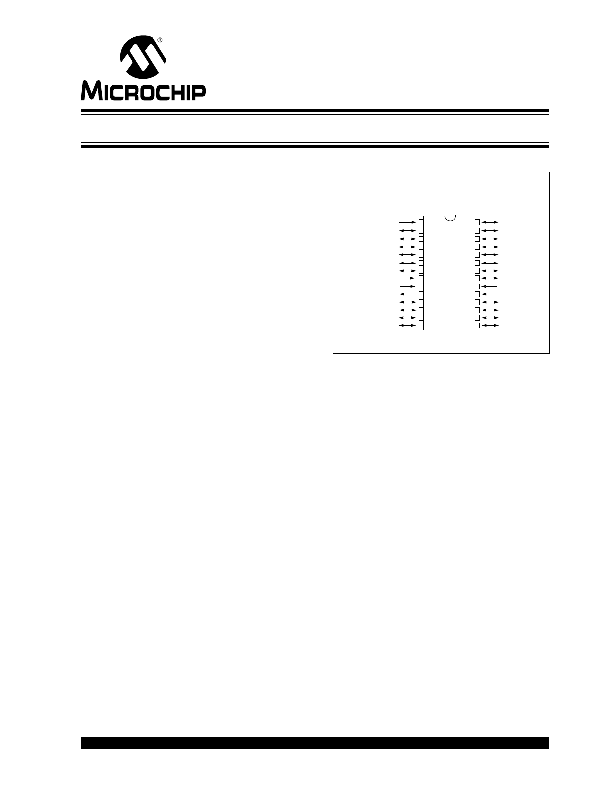
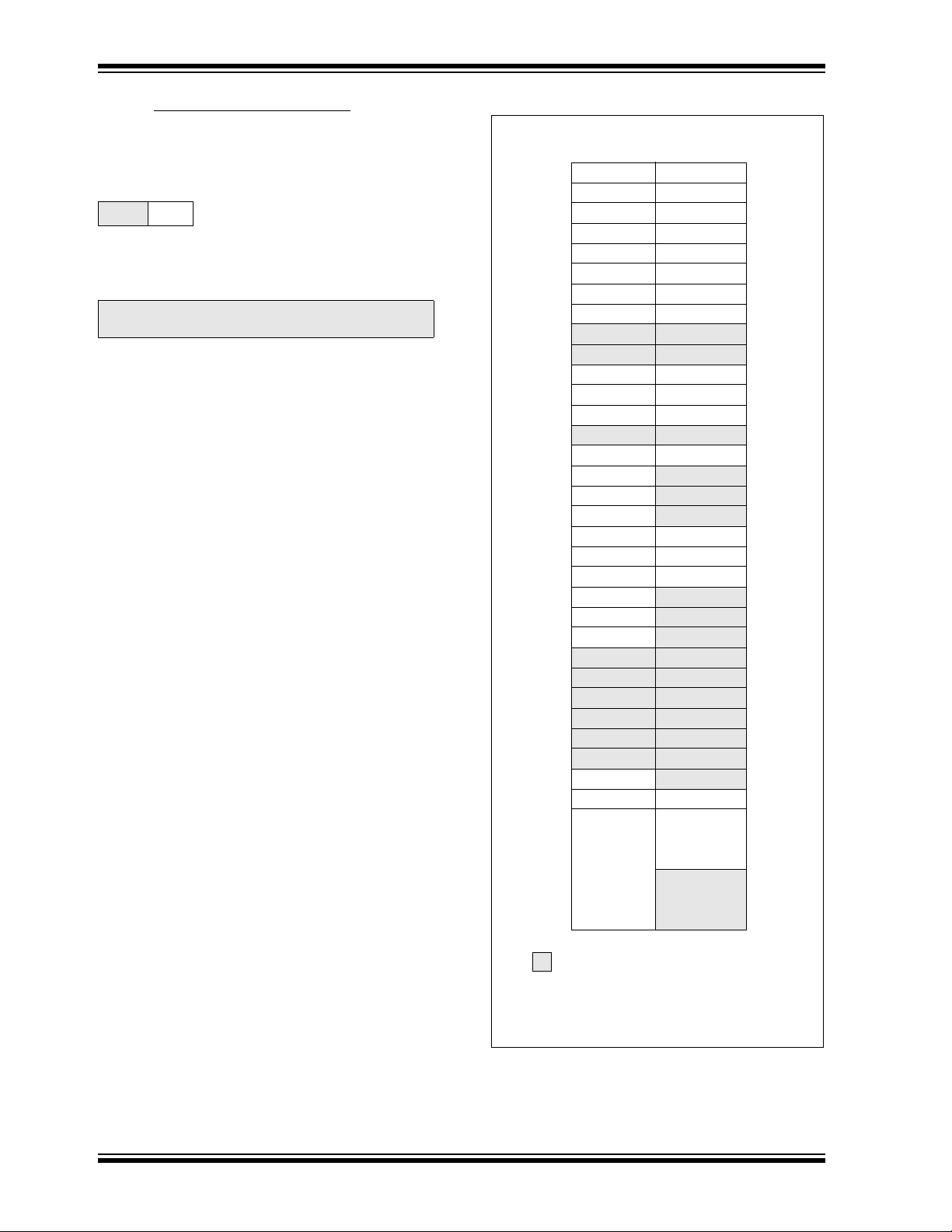
PIC16C72A
MCLR/VPP
RA0/AN0
RA1/AN1
RA2/AN2
RA3/AN3/V
REF
RA4/T0CKI
RA5/SS/AN4
V
SS
OSC1/CLKIN
OSC2/CLKOUT
RC0/T1OSO/T1CKI
RC1/T1OSI
RC2/CCP1
RC3/SCK/SCL
RB7
RB6
RB5
RB4
RB3
RB2
RB1
RB0/INT
V
DD
VSS
RC7
RC6
RC5/SDO
RC4/SDI/SDA
• 1
2
3
4
5
6
7
8
9
10
11
12
13
14
28
27
26
25
24
23
22
21
20
19
18
17
16
15
SDIP, SOIC, SSOP, Windowed CERDIP
PIC16C62B/72A
28-Pin 8-Bit CMOS Microcontrollers
Microcontroller Core Features:
• High-performance RISC CPU
• Only 35 single word instructions to learn
• All single cycle instructions except for program
branches, which are two cycle
• Operating speed: DC - 20 MHz clock input
DC - 200 ns instruction cycle
• 2K x 14 words of Program Memory,
128 x 8 bytes of Data Memory (RAM)
• Interrupt capability
• Eight level deep hardware stack
• Direct, indirect, and relative addressing modes
• Power-on Reset (POR)
• Power-up Timer (PWRT) and
Oscillator Start-up Timer (OST)
• Watchdog Timer (WDT) with its own on-chip RC
oscillator for reliable operation
• Brown-out detection circuitry for
Brown-out Reset (BOR)
• Programmable code-protection
• Power saving SLEEP mode
• Selectable oscillator options
• Low-power, high-speed CMOS EPROM
technology
• Fully static design
• In-Circuit Serial Programming(ICSP)
• Wide operating voltage range: 2.5V to 5.5V
• High Sink/Source Current 25/25 mA
• Commercial, Industrial and Extended temperature
ranges
• Low-power consumption:
- < 2 mA @ 5V, 4 MHz
- 22.5 A typical @ 3V, 32 kHz
-< 1 A typical standby current
Pin Diagram
Peripheral Features:
• Timer0: 8-bit timer/counter with 8-bit prescaler
• Timer1: 16-bit timer/counter with prescaler,
can be incremented during sleep via external
crystal/clock
• Timer2: 8-bit timer/counter with 8-bit period
register, prescaler and postscaler
• Capture, Compare, PWM module
• Capture is 16-bit, max. resolution is 12.5 ns,
Compare is 16-bit, max. resolution is 200 ns,
PWM maximum resolution is 10-bit
• 8-bit multi-channel Analog-to-Digital converter
• Synchronous Serial Port (SSP) with Enhanced
SPI and I
2C
1998-2013 Microchip Technology Inc. Preliminary DS35008C-page 1
Page 2
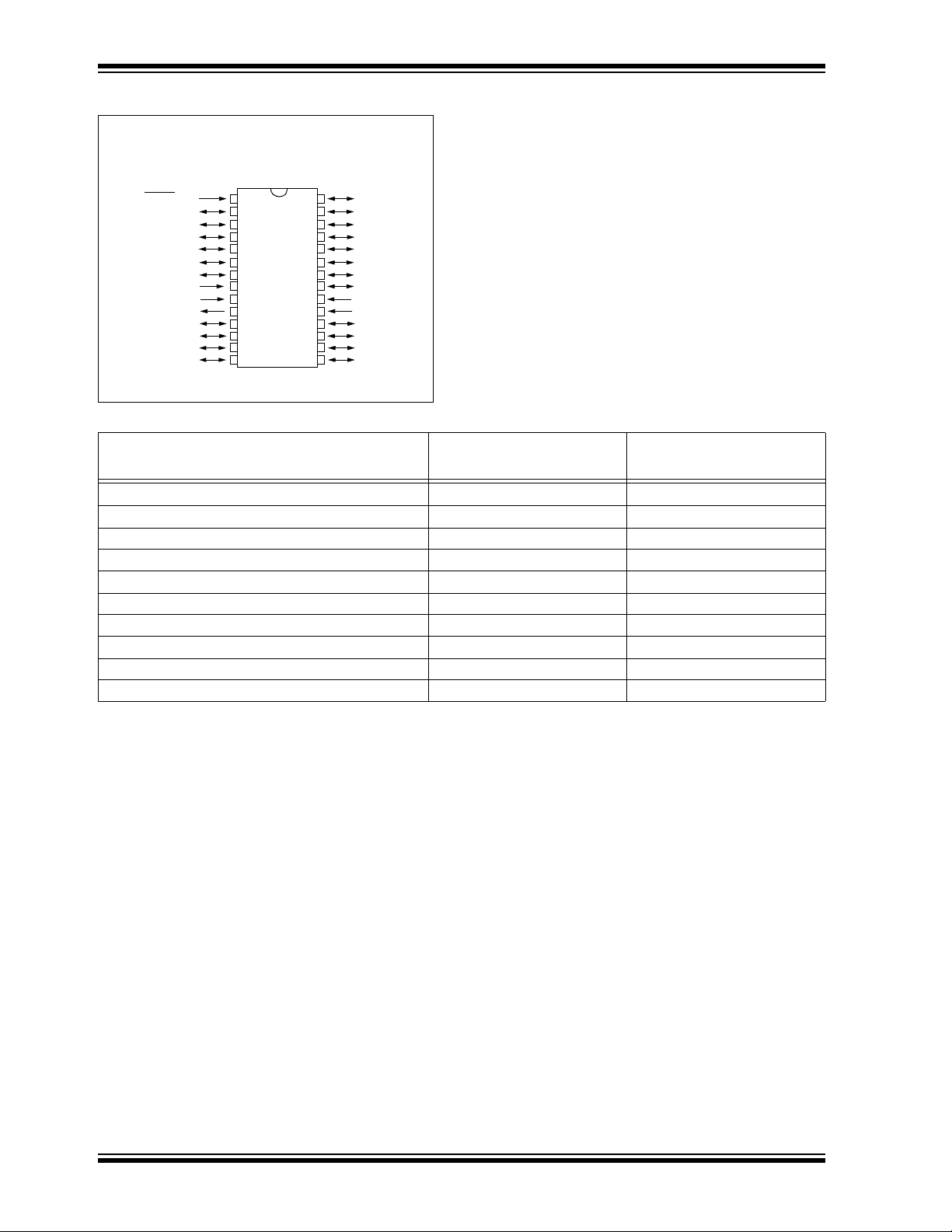
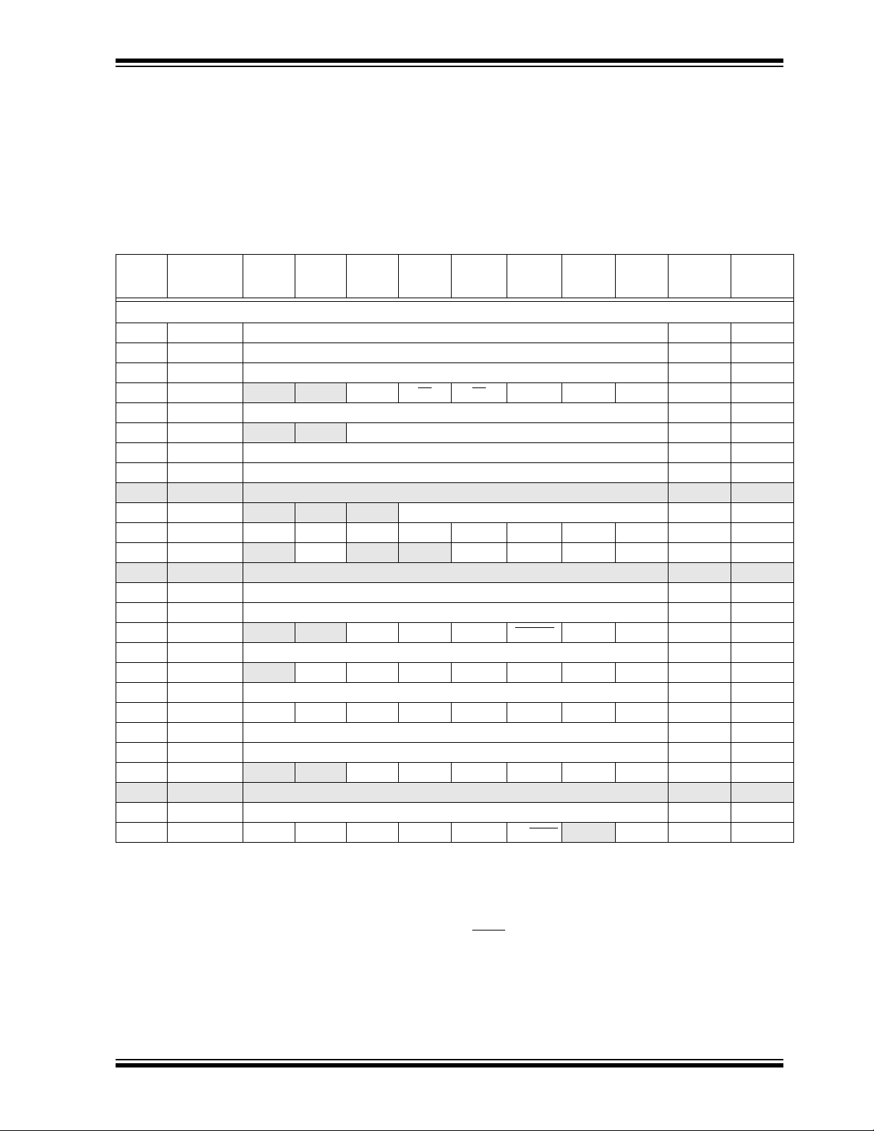
PIC16C62B/72A
PIC16C62B
MCLR/VPP
RA0
RA1
RA2
RA3
RA4/T0CKI
RA5/SS
V
SS
OSC1/CLKIN
OSC2/CLKOUT
RC0/T1OSO/T1CKI
RC1/T1OSI
RC2/CCP1
RC3/SCK/SCL
RB7
RB6
RB5
RB4
RB3
RB2
RB1
RB0/INT
V
DD
VSS
RC7
RC6
RC5/SDO
RC4/SDI/SDA
• 1
2
3
4
5
6
7
8
9
10
11
12
13
14
28
27
26
25
24
23
22
21
20
19
18
17
16
15
SDIP, SOIC, SSOP, Windowed CERDIP
Pin Diagrams
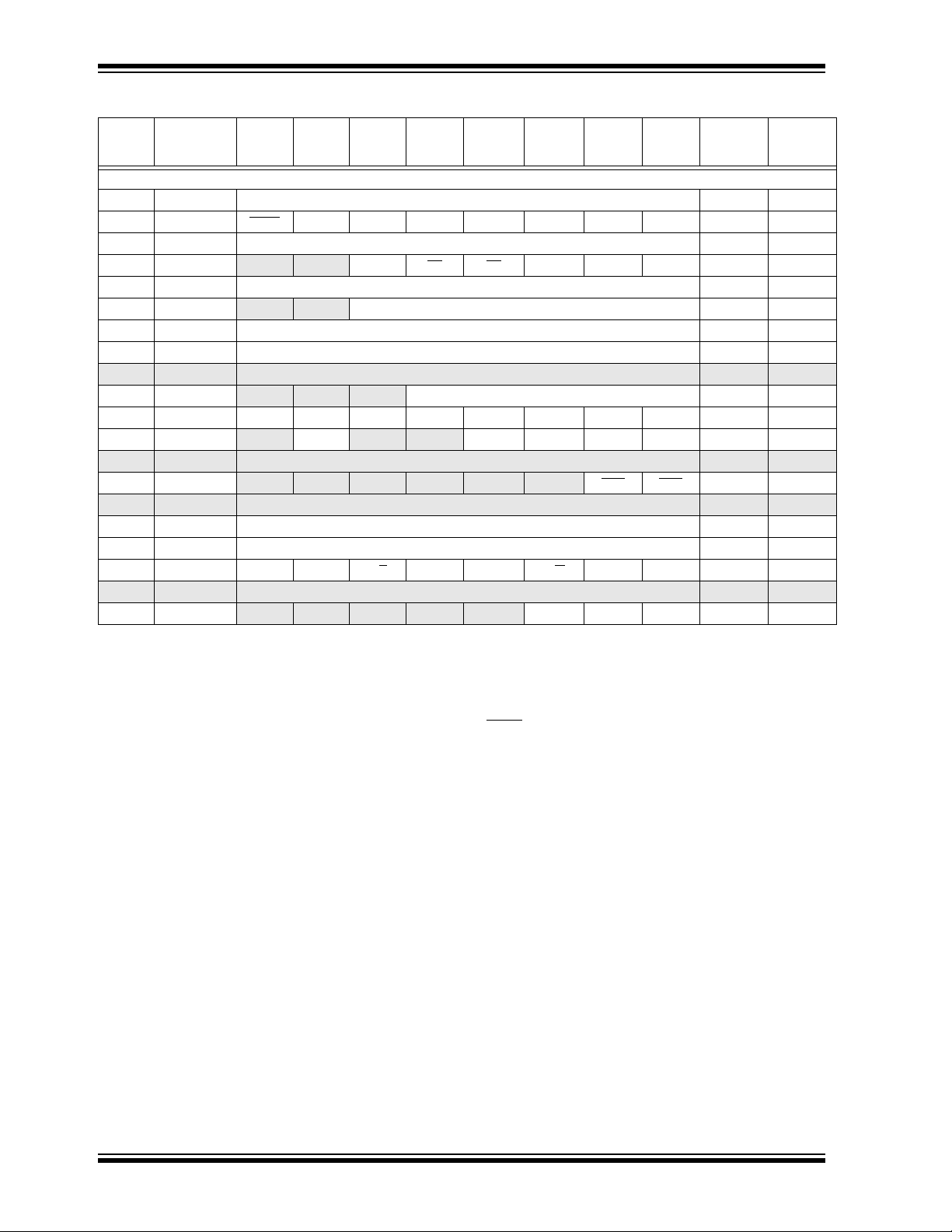
Key Features
PIC® Mid-Range Reference Manual (DS33023)
PIC16C62B PIC16C72A
Operating Frequency DC - 20 MHz DC - 20 MHz
Resets (and Delays) POR, BOR (PWRT, OST) POR, BOR (PWRT, OST)
Program Memory (14-bit words) 2K 2K
Data Memory (bytes) 128 128
Interrupts 7 8
I/O Ports Ports A,B,C Ports A,B,C
Timers 3 3
Capture/Compare/PWM modules 1 1
Serial Communications SSP SSP
8-bit Analog-to-Digital Module — 5 input channels
DS35008C-page 2 Preliminary 1998-2013 Microchip Technology Inc.
Page 3

PIC16C62B/72A
Table of Contents
1.0 Device Overview .................................................................................................................................................... 5
2.0 Memory Organization............................................................................................................................................. 7
3.0 I/O Ports ............................................................................................................................................................... 19
4.0 Timer0 Module ..................................................................................................................................................... 25
5.0 Timer1 Module ..................................................................................................................................................... 27
6.0 Timer2 Module ..................................................................................................................................................... 31
7.0 Capture/Compare/PWM (CCP) Module ............................................................................................................... 33
8.0 Synchronous Serial Port (SSP) Module ............................................................................................................... 39
9.0 Analog-to-Digital Converter (A/D) Module............................................................................................................ 49
10.0 Special Features of the CPU................................................................................................................................ 55
11.0 Instruction Set Summary ...................................................................................................................................... 67
12.0 Development Support........................................................................................................................................... 75
13.0 Electrical Characteristics...................................................................................................................................... 81
14.0 DC and AC Characteristics Graphs and Tables................................................................................................. 103
15.0 Packaging Information........................................................................................................................................ 105
Appendix A: Revision History ................................................................................................................................... 111
Appendix B: Conversion Considerations .................................................................................................................. 111
Appendix C: Migration from Base-line to Mid-Range Devices .................................................................................. 112
Index ...........................................................................................................................................................................113
On-Line Support.......................................................................................................................................................... 117
Reader Response....................................................................................................................................................... 118
PIC16C62B/72A Product Identification System .......................................................................................................... 119
To Our Valued Customers
Most Current Data Sheet
To obtain the most up-to-date version of this data sheet, please register at our Worldwide Web site at:
http://www.microchip.com
You can determine the version of a data sheet by examining its literature number found on the bottom outside corner of any page.
The last character of the literature number is the version number. e.g., DS30000A is version A of document DS30000.
New Customer Notification System
Register on our web site (www.microchip.com/cn) to receive the most current information on our products.
Errata
An errata sheet may exist for current devices, describing minor operational differences (from the data sheet) and recommended
workarounds. As device/documentation issues become known to us, we will publish an errata sheet. The errata will specify the revision of silicon and revision of document to which it applies.
To determine if an errata sheet exists for a particular device, please check with one of the following:
• Microchip’s Worldwide Web site; http://www.microchip.com
• Your local Microchip sales office (see last page)
• The Microchip Corporate Literature Center; U.S. FAX: (480) 786-7277
When contacting a sales office or the literature center, please specify which device, revision of silicon and data sheet (include literature number) you are using.
Corrections to this Data Sheet
We constantly strive to improve the quality of all our products and documentation. We have spent a great deal of time to ensure that
this document is correct. However, we realize that we may have missed a few things. If you find any information that is missing or
appears in error, please:
• Fill out and mail in the reader response form in the back of this data sheet.
• E-mail us at webmaster@microchip.com.
We appreciate your assistance in making this a better document.
1998-2013 Microchip Technology Inc. Preliminary DS35008C-page 3
Page 4

PIC16C62B/72A
NOTES:
DS35008C-page 4 Preliminary 1998-2013 Microchip Technology Inc.
Page 5
PIC16C62B/72A
EPROM
Program
Memory
13
Data Bus
8
14
Program
Bus
Instruction reg
Program Counter
8 Level Stack
(13-bit)
RAM
File
Registers
Direct Addr
7
RAM Addr
(1)
9
Addr MUX
Indirect
Addr
FSR reg
STATUS reg
MUX
ALU
W reg
Power-up
Timer
Oscillator
Start-up Timer
Power-on
Reset
Watchdog
Timer
Instruction
Decode &
Control
Timing
Generation
OSC1/CLKIN
OSC2/CLKOUT
MCLR
VDD, VSS
PORTA
PORTB
PORTC
RB0/INT
RB7:RB1
RC0/T1OSO/T1CKI
RC1/T1OSI
RC2/CCP1
RC3/SCK/SCL
RC4/SDI/SDA
RC5/SDO
RC6
RC7
8
8
Brown-out
Reset
Note 1: Higher order bits are from the STATUS register.
2: The A/D module is not available on the PIC16C62B.
CCP1
Synchronous
A/D
(2)
Timer0 Timer1 Timer2
Serial Port
RA4/T0CKI
RA5/SS
/AN4
(2)
RA3/AN3/VREF
(2)
RA2/AN2
(2)
RA1/AN1
(2)
RA0/AN0
(2)
8
3
2K x 14
128 x 8
1.0 DEVICE OVERVIEW
This document contains device-specific information.
Additional information may be found in the PIC
Mid-Range Reference Manual, (DS33023), which may
be obtained from your local Microchip Sales Representative or downloaded from the Microchip website. The
Reference Manual should be considered a complementary document to this data sheet, and is highly rec-
FIGURE 1-1: PIC16C62B/PIC16C72A BLOCK DIAGRAM
®
MCU
ommended reading for a better understanding of the
device architecture and operation of the peripheral
modules.
There are two devices (PIC16C62B, PIC16C72A) covered by this datasheet. The PIC16C62B does not have
the A/D module implemented.
Figure 1-1 is the block diagram for both devices. The
pinouts are listed in Table 1-1.
1998-2013 Microchip Technology Inc. Preliminary DS35008C-page 5
Page 6

PIC16C62B/72A
TABLE 1-1 PIC16C62B/PIC16C72A PINOUT DESCRIPTION
Pin Name
DIP
Pin#
OSC1/CLKIN 9 9 I
SOIC
Pin#
I/O/P
Typ e
Buffer
Typ e
ST/CMOS
Description
(3)
Oscillator crystal input/external clock source input.
OSC2/CLKOUT 10 10 O — Oscillator crystal output. Connects to crystal or resonator in
crystal oscillator mode. In RC mode, the OSC2 pin outputs
CLKOUT which has 1/4 the frequency of OSC1, and denotes
the instruction cycle rate.
MCLR
/VPP
1 1 I/P ST Master clear (reset) input or programming voltage input. This
pin is an active low reset to the device.
PORTA is a bi-directional I/O port.
RA0/AN0
RA1/AN1
RA2/AN2
RA3/AN3/V
(4)
(4)
(4)
(4)
REF
2 2 I/O TTL RA0 can also be analog input 0
3 3 I/O TTL RA1 can also be analog input 1
4 4 I/O TTL RA2 can also be analog input 2
5 5 I/O TTL RA3 can also be analog input 3 or analog reference voltage
RA4/T0CKI 6 6 I/O ST RA4 can also be the clock input to the Timer0 module.
Output is open drain type.
RA5/SS/
AN4
(4)
7 7 I/O TTL RA5 can also be analog input 4 or the slave select for the
synchronous serial port.
PORTB is a bi-directional I/O port. PORTB can be software
programmed for internal weak pull-up on all inputs.
RB0/INT 21 21 I/O TTL/ST
(1)
RB0 can also be the external interrupt pin.
RB1 22 22 I/O TTL
RB2 23 23 I/O TTL
RB3 24 24 I/O TTL
RB4 25 25 I/O TTL Interrupt on change pin.
RB5 26 26 I/O TTL Interrupt on change pin.
RB6 27 27 I/O TTL/ST
RB7 28 28 I/O TTL/ST
(2)
(2)
Interrupt on change pin. Serial programming clock.
Interrupt on change pin. Serial programming data.
PORTC is a bi-directional I/O port.
RC0/T1OSO/T1CKI 11 11 I/O ST RC0 can also be the Timer1 oscillator output or Timer1
clock input.
RC1/T1OSI 12 12 I/O ST RC1 can also be the Timer1 oscillator input.
RC2/CCP1 13 13 I/O ST RC2 can also be the Capture1 input/Compare1 output/
PWM1 output.
RC3/SCK/SCL 14 14 I/O ST RC3 can also be the synchronous serial clock input/output
for both SPI and I
RC4/SDI/SDA 15 15 I/O ST RC4 can also be the SPI Data In (SPI mode) or
data I/O (I
2
C mode).
2
C modes.
RC5/SDO 16 16 I/O ST RC5 can also be the SPI Data Out (SPI mode).
RC6 17 17 I/O ST
RC7 18 18 I/O ST
SS 8, 19 8, 19 P — Ground reference for logic and I/O pins.
V
DD 20 20 P — Positive supply for logic and I/O pins.
V
Legend: I = input O = output I/O = input/output P = power or program
— = Not used TTL = TTL input ST = Schmitt Trigger input
Note 1: This buffer is a Schmitt Trigger input when configured as the external interrupt.
2: This buffer is a Schmitt Trigger input when used in serial programming mode.
3: This buffer is a Schmitt Trigger input when configured in RC oscillator mode and a CMOS input otherwise.
4: The A/D module is not available on the PIC16C62B.
DS35008C-page 6 Preliminary 1998-2013 Microchip Technology Inc.
Page 7
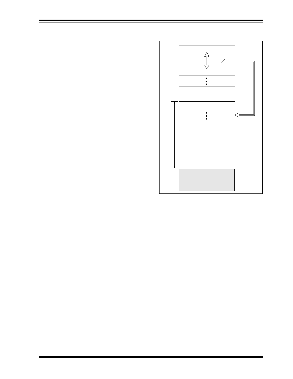
PIC16C62B/72A
PC<12:0>
13
0000h
0004h
0005h
07FFh
0800h
1FFFh
Stack Level 1
Stack Level 8
Reset Vector
Interrupt Vector
On-chip Program
Memory
CALL, RETURN
RETFIE, RETLW
User Memory
Space
2.0 MEMORY ORGANIZATION
There are two memory blocks in each of these microcontrollers. Each block (Program Memory and Data
Memory) has its own bus, so that concurrent access
can occur.
Additional information on device memory may be found
in the PICmicro Mid-Range Reference Manual,
(DS33023).
2.1 Program Memory Organization
The PIC16C62B/72A devices have a 13-bit program
counter capable of addressing an 8K x 14 program
memory space. Each device has 2K x 14 words of program memory. Accessing a location above 07FFh will
cause a wraparound.
The reset vector is at 0000h and the interrupt vector is
at 0004h.
FIGURE 2-1: PROGRAM MEMORY MAP
AND STACK
1998-2013 Microchip Technology Inc. Preliminary DS35008C-page 7
Page 8
PIC16C62B/72A
Unimplemented data memory locations,
read as '0'.
Note 1: Not a physical register.
2: These registers are not implemented on the
PIC16C62B, read as '0'.
File
Address
File
Address
00h INDF
(1)
INDF
(1)
80h
01h TMR0 OPTION_REG 81h
02h PCL PCL 82h
0 3 h S TATU S S TAT U S 8 3 h
04h FSR FSR 84h
05h PORTA TRISA 85h
06h PORTB TRISB 86h
07h PORTC TRISC 87h
08h
— — 88h
09h
— — 89h
0Ah PCLATH PCLATH 8Ah
0Bh INTCON INTCON 8Bh
0Ch PIR1 PIE1 8Ch
0Dh
— — 8Dh
0Eh TMR1L PCON 8Eh
0Fh TMR1H
— 8Fh
10h T1CON
— 90h
11h TMR2
— 91h
12h T2CON PR2 92h
13h SSPBUF SSPADD 93h
14h SSPCON SSPSTAT 94h
15h CCPR1L
— 95h
16h CCPR1H
— 96h
17h CCP1CON
— 97h
18h
— — 98h
19h
— — 99h
1Ah
— — 9Ah
1Bh
— — 9Bh
1Ch
— — 9Ch
1Dh
— — 9Dh
1Eh ADRES
(2)
— 9Eh
1Fh ADCON0
(2)
ADCON1
(2)
9Fh
20h
General
Purpose
Registers
General
Purpose
Registers
A0h
BFh
—
C0h
—
7Fh
—
FFh
Bank 0 Bank 1
2.2 Data Memory Organization
The data memory is partitioned into multiple banks
which contain the General Purpose Registers and the
Special Function Registers. Bits RP1 and RP0 are the
bank select bits.
(1)
RP1
= 00 Bank0
= 01 Bank1
= 10 Bank2 (not implemented)
= 11 Bank3 (not implemented)
Note 1: Maintain this bit clear to ensure upward compati-
Each bank extends up to 7Fh (128 bytes). The lower
locations of each bank are reserved for the Special
Function Registers. Above the Special Function Registers are General Purpose Registers, implemented as
static RAM. All implemented banks contain Special
Function Registers. Some “high use” Special Function
Registers from one bank may be mirrored in another
bank for code reduction and quicker access.
2.2.1 GENERAL PURPOSE REGISTER FILE
The register file can be accessed either directly, or indirectly through the File Select Register FSR
(Section 2.5).
DS35008C-page 8 Preliminary 1998-2013 Microchip Technology Inc.
RP0 (STATUS<6:5>)
bility with future products.
FIGURE 2-2: REGISTER FILE MAP
Page 9
PIC16C62B/72A
2.2.2 SPECIAL FUNCTION REGISTERS
The Special Function Registers can be classified into
two sets; core (CPU) and peripheral. Those registers
The Special Function Registers are registers used by
the CPU and Peripheral Modules for controlling the
desired operation of the device. These registers are
implemented as static RAM. A list of these registers is
given in Table 2-1.
associated with the core functions are described in
detail in this section. Those related to the operation of
the peripheral features are described in detail in the
peripheral feature section.
TABLE 2-1 SPECIAL FUNCTION REGISTER SUMMARY
Addr Name Bit 7 Bit 6 Bit 5 Bit 4 Bit 3 Bit 2 Bit 1 Bit 0
Val ue on:
POR,
BOR
Bank 0
00h INDF
01h TMR0 Timer0 module’s register xxxx xxxx uuuu uuuu
02h PCL
03h STATUS
04h FSR
05h PORTA
06h PORTB
07h PORTC
08h-09h — Unimplemented — —
0Ah PCLATH
0Bh INTCON
0Ch PIR1
0Dh — Unimplemented — —
0Eh TMR1L Holding register for the Least Significant Byte of the 16-bit TMR1 register xxxx xxxx uuuu uuuu
0Fh TMR1H Holding register for the Most Significant Byte of the 16-bit TMR1 register xxxx xxxx uuuu uuuu
10h T1CON
11h TMR2 Timer2 module’s register 0000 0000 0000 0000
12h T2CON
13h SSPBUF Synchronous Serial Port Receive Buffer/Transmit Register xxxx xxxx uuuu uuuu
14h SSPCON WCOL SSPOV SSPEN CKP SSPM3 SSPM2 SSPM1 SSPM0 0000 0000 0000 0000
15h CCPR1L Capture/Compare/PWM Register1 (LSB) xxxx xxxx uuuu uuuu
16h CCPR1H Capture/Compare/PWM Register1 (MSB) xxxx xxxx uuuu uuuu
17h CCP1CON
18h-1Dh — Unimplemented — —
1Eh ADRES
1Fh ADCON0
Legend: x = unknown, u = unchanged, q = value depends on condition, - = unimplemented, read as '0',
Note 1: These registers can be addressed from either bank.
2: The upper byte of the program counter is not directly accessible. PCLATH is a holding register for PC<12:8> whose contents
3: A/D not implemented on the PIC16C62B, maintain as ’0’.
4: Other (non power-up) resets include: external reset through MCLR
5: The IRP and RP1 bits are reserved. Always maintain these bits clear.
6: On any device reset, these pins are configured as inputs.
7: This is the value that will be in the port output latch.
(1)
(1)
(1)
Addressing this location uses contents of FSR to address data memory (not a physical register) 0000 0000 0000 0000
Program Counter's (PC) Least Significant Byte 0000 0000 0000 0000
(1)
(6,7)
(6,7)
(6,7)
(1,2)
(1)
(3)
(3)
(5)
IRP
Indirect data memory address pointer xxxx xxxx uuuu uuuu
— — PORTA Data Latch when written: PORTA pins when read --0x 0000 --0u 0000
PORTB Data Latch when written: PORTB pins when read xxxx xxxx uuuu uuuu
PORTC Data Latch when written: PORTC pins when read xxxx xxxx uuuu uuuu
— — — Write Buffer for the upper 5 bits of the Program Counter ---0 0000 ---0 0000
GIE PEIE T0IE INTE RBIE T0IF INTF RBIF 0000 000x 0000 000u
—ADIF
— — T1CKPS1 T1CKPS0 T1OSCEN T1SYNC TMR1CS TMR1ON --00 0000 --uu uuuu
— TOUTPS3 TOUTPS2 TOUTPS1 TOUTPS0 TMR2ON T2CKPS1 T2CKPS0 -000 0000 -000 0000
— — CCP1X CCP1Y CCP1M3 CCP1M2 CCP1M1 CCP1M0 --00 0000 --00 0000
A/D Result Register xxxx xxxx uuuu uuuu
ADCS1 ADCS0 CHS2 CHS1 CHS0 GO/DONE —ADON0000 00-0 0000 00-0
RP1
(5)
RP0 TO PD ZDCC0001 1xxx 000q quuu
(3)
— — SSPIF CCP1IF TMR2IF TMR1IF -0-- 0000 -0-- 0000
Shaded locations are unimplemented, read as '0'.
are transferred to the upper byte of the program counter.
and the Watchdog Timer Reset.
Value on all
other resets
(4)
1998-2013 Microchip Technology Inc. Preliminary DS35008C-page 9
Page 10
PIC16C62B/72A
TABLE 2-1 SPECIAL FUNCTION REGISTER SUMMARY (Cont.’d)
Addr Name Bit 7 Bit 6 Bit 5 Bit 4 Bit 3 Bit 2 Bit 1 Bit 0
Bank 1
80h INDF
81h OPTION_REG RBPU INTEDG T0CS T0SE PSA PS2 PS1 PS0 1111 1111 1111 1111
82h PCL
83h STATUS
84h FSR
85h TRISA
86h TRISB PORTB Data Direction Register 1111 1111 1111 1111
87h TRISC PORTC Data Direction Register 1111 1111 1111 1111
88h-89h — Unimplemented — —
8Ah PCLATH
8Bh INTCON
8Ch PIE1
8Dh — Unimplemented — —
8Eh PCON — — — — — —PORBOR ---- --qq ---- --uu
8Fh-91h — Unimplemented — —
92h PR2 Timer2 Period Register 1111 1111 1111 1111
93h SSPADD Synchronous Serial Port (I
94h SSPSTAT SMP CKE D/A
95h-9Eh — Unimplemented — —
9Fh ADCON1
(1)
(1)
(1)
Addressing this location uses contents of FSR to address data memory (not a physical register) 0000 0000 0000 0000
Program Counter's (PC) Least Significant Byte 0000 0000 0000 0000
(1)
(1,2)
(1)
(3)
(5)
IRP
Indirect data memory address pointer xxxx xxxx uuuu uuuu
— — PORTA Data Direction Register --11 1111 --11 1111
— — — Write Buffer for the upper 5 bits of the Program Counter ---0 0000 ---0 0000
GIE PEIE T0IE INTE RBIE T0IF INTF RBIF 0000 000x 0000 000u
—ADIE
— — — — — PCFG2 PCFG1 PCFG0 ---- -000 ---- -000
RP1
(5)
RP0 TO PD ZDCC0001 1xxx 000q quuu
(3)
— — SSPIE CCP1IE TMR2IE TMR1IE -0-- 0000 -0-- 0000
2
C mode) Address Register 0000 0000 0000 0000
PSR/WUA B F 0000 0000 0000 0000
Val ue on:
POR,
BOR
Legend: x = unknown, u = unchanged, q = value depends on condition, - = unimplemented, read as '0',
Shaded locations are unimplemented, read as '0'.
Note 1: These registers can be addressed from either bank.
2: The upper byte of the program counter is not directly accessible. PCLATH is a holding register for PC<12:8> whose contents
are transferred to the upper byte of the program counter.
3: A/D not implemented on the PIC16C62B, maintain as ’0’.
4: Other (non power-up) resets include: external reset through MCLR
and the Watchdog Timer Reset.
5: The IRP and RP1 bits are reserved. Always maintain these bits clear.
6: On any device reset, these pins are configured as inputs.
7: This is the value that will be in the port output latch.
Value on all
other resets
(4)
DS35008C-page 10 Preliminary 1998-2013 Microchip Technology Inc.
Page 11

PIC16C62B/72A
2.2.2.1 STATUS REGISTER
The STATUS register, shown in Register 2-1, contains
the arithmetic status of the ALU, the RESET status and
the bank select bits for data memory.
The STATUS register can be the destination for any
instruction, as with any other register. If the STATUS
register is the destination for an instruction that affects
the Z, DC or C bits, the write to these three bits is disabled. These bits are set or cleared according to the
device logic. The TO
result of an instruction with the STATUS register as
destination may be different than intended.
For example, CLRF STATUS will clear the upper-three
bits and set the Z bit. This leaves the STATUS register
as 000u u1uu (where u = unchanged).
and PD bits are not writable. The
It is recommended, therefore, that only BCF, BSF,
SWAPF and MOVWF instructions are used to alter the
STATUS register, because these instructions do not
affect the Z, C or DC bits from the STATUS register. For
other instructions, not affecting any status bits, see the
"Instruction Set Summary."
Note 1: The IRP and RP1 bits are reserved. Main-
tain these bits clear to ensure upward
compatibility with future products.
Note 2: The C and DC bits operate as a borrow
and digit borrow bit, respectively, in subtraction. See the SUBLW and SUBWF
instructions.
REGISTER 2-1: STATUS REGISTER (ADDRESS 03h, 83h)
R/W-0 R/W-0 R/W-0 R-1 R-1 R/W-x R/W-x R/W-x
IRP RP1 RP0 TO PD Z DC C R = Readable bit
bit7 bit0
bit 7: IRP: Register Bank Select bit (used for indirect addressing)
(reserved, maintain clear)
bit 6-5: RP1:RP0: Register Bank Select bits (used for direct addressing)
01 = Bank 1 (80h - FFh)
00 = Bank 0 (00h - 7Fh)
Each bank is 128 bytes
Note: RP1 is reserved, maintain clear
bit 4: TO
bit 3: PD
bit 2: Z: Zero bit
bit 1: DC: Digit carry/borrow
bit 0: C: Carry/borrow
: Time-out bit
1 = After power-up, CLRWDT instruction, or SLEEP instruction
0 = A WDT time-out occurred
: Power-down bit
1 = After power-up or by the CLRWDT instruction
0 = By execution of the SLEEP instruction
1 = The result of an arithmetic or logic operation is zero
0 = The result of an arithmetic or logic operation is not zero
bit (ADDWF, ADDLW,SUBLW,SUBWF instructions) (for borrow, the polarity is reversed)
1 = A carry-out from the 4th low order bit of the result occurred
0 = No carry-out from the 4th low order bit of the result
bit (ADDWF, ADDLW,SUBLW,SUBWF instructions) (for borrow, the polarity is reversed)
1 = A carry-out from the most significant bit of the result occurred
0 = No carry-out from the most significant bit of the result occurred
W = Writable bit
U = Unimplemented bit,
read as ‘0’
- n = Value at POR reset
Note: For borrow
second operand. For rotate (RRF, RLF) instructions, this bit is loaded with either the high or low order bit of
the source register.
1998-2013 Microchip Technology Inc. Preliminary DS35008C-page 11
, the polarity is reversed. A subtraction is executed by adding the two’s complement of the
Page 12

PIC16C62B/72A
000
001
010
011
100
101
110
111
1 : 2
1 : 4
1 : 8
1 : 16
1 : 32
1 : 64
1 : 128
1 : 256
1 : 1
1 : 2
1 : 4
1 : 8
1 : 16
1 : 32
1 : 64
1 : 128
Bit Value TMR0 Rate WDT Rate
2.2.2.2 OPTION_REG REGISTER
The OPTION_REG register is a readable and writable
register, which contains various control bits to configure
the TMR0 prescaler/WDT postscaler (single assignable register known as the prescaler), the External INT
Interrupt, TMR0 and the weak pull-ups on PORTB.
REGISTER 2-2: OPTION_REG REGISTER (ADDRESS 81h)
R/W-1 R/W-1 R /W-1 R/W-1 R/W-1 R/W-1 R/W-1 R/W-1
RBPU
bit7 bit0
bit 7: RBPU: PORTB Pull-up Enable bit
bit 6: INTEDG: Interrupt Edge Select bit
bit 5: T0CS: TMR0 Clock Source Select bit
bit 4: T0SE: TMR0 Source Edge Select bit
bit 3: PSA: Prescaler Assignment bit
bit 2-0: PS2:PS0: Prescaler Rate Select bits
INTEDG T0CS T0SE PSA PS2 PS1 PS0 R = Readable bit
1 = PORTB pull-ups are disabled
0 = PORTB pull-ups are enabled for all PORTB inputs
1 = Interrupt on rising edge of RB0/INT pin
0 = Interrupt on falling edge of RB0/INT pin
1 = Transition on RA4/T0CKI pin
0 = Internal instruction cycle clock (CLKOUT)
1 = Increment on high-to-low transition on RA4/T0CKI pin
0 = Increment on low-to-high transition on RA4/T0CKI pin
1 = Prescaler is assigned to the WDT
0 = Prescaler is assigned to the Timer0 module
Note: To achieve a 1:1 prescaler assignment for
the TMR0 register, assign the prescaler to
the Watchdog Timer.
W = Writable bit
- n = Value at POR reset
DS35008C-page 12 Preliminary 1998-2013 Microchip Technology Inc.
Page 13

PIC16C62B/72A
2.2.2.3 INTCON REGISTER
The INTCON Register is a readable and writable register, which contains various interrupt enable and flag
bits for the TMR0 register overflow, RB Port change
and External RB0/INT pin interrupts.
Note: Interrupt flag bits are set when an interrupt
condition occurs, regardless of the state of
its corresponding enable bit or the global
enable bit, GIE (INTCON<7>). User software should ensure the appropriate interrupt flag bits are clear prior to enabling an
interrupt.
REGISTER 2-3: INTCON REGISTER (ADDRESS 0Bh, 8Bh)
R/W-0 R/W-0 R /W-0 R/W-0 R/W-0 R/W-0 R/W-0 R/W-x
GIE PEIE T0IE INTE RBIE T0IF INTF RBIF R = Readable bit
bit7 bit0
bit 7: GIE: Global Interrupt Enable bit
1 = Enables all un-masked interrupts
0 = Disables all interrupts
bit 6: PEIE: Peripheral Interrupt Enable bit
1 = Enables all un-masked peripheral interrupts
0 = Disables all peripheral interrupts
bit 5: T0IE: TMR0 Overflow Interrupt Enable bit
1 = Enables the TMR0 interrupt
0 = Disables the TMR0 interrupt
bit 4: IINTE: RB0/INT External Interrupt Enable bit
1 = Enables the RB0/INT external interrupt
0 = Disables the RB0/INT external interrupt
bit 3: RBIE: RB Port Change Interrupt Enable bit
1 = Enables the RB port change interrupt
0 = Disables the RB port change interrupt
bit 2: T0IF: TMR0 Overflow Interrupt Flag bit
1 = TMR0 register has overflowed (software must clear bit)
0 = TMR0 register did not overflow
bit 1: INTF: RB0/INT External Interrupt Flag bit
1 = The RB0/INT external interrupt occurred (software must clear bit)
0 = The RB0/INT external interrupt did not occur
bit 0: RBIF: RB Port Change Interrupt Flag bit
1 = At least one of the RB7:RB4 input pins have changed state (clear by reading PORTB)
0 = None of the RB7:RB4 input pins have changed state
W = Writable bit
- n = Value at POR reset
1998-2013 Microchip Technology Inc. Preliminary DS35008C-page 13
Page 14

PIC16C62B/72A
2.2.2.4 PIE1 REGISTER
This register contains the individual enable bits for the
Note: Bit PEIE (INTCON<6>) must be set to
enable any peripheral interrupt.
peripheral interrupts.
REGISTER 2-4: PIE1 REGISTER (ADDRESS 8Ch)
U-0 R/W-0 U-0 U-0 R/W-0 R/W-0 R/W-0 R/W-0
— ADIE
bit7 bit0
bit 7: Unimplemented: Read as ‘0’
bit 6: ADIE
bit 5-4: Unimplemented: Read as ‘0’
bit 3: SSPIE: Synchronous Serial Port Interrupt Enable bit
bit 2: CCP1IE: CCP1 Interrupt Enable bit
bit 1: TMR2IE: TMR2 to PR2 Match Interrupt Enable bit
bit 0: TMR1IE: TMR1 Overflow Interrupt Enable bit
(1)
— — SSPIE CCP1IE TMR2IE TMR1IE R = Readable bit
(1)
: A/D Converter Interrupt Enable bit
1 = Enables the A/D interrupt
0 = Disables the A/D interrupt
1 = Enables the SSP interrupt
0 = Disables the SSP interrupt
1 = Enables the CCP1 interrupt
0 = Disables the CCP1 interrupt
1 = Enables the TMR2 to PR2 match interrupt
0 = Disables the TMR2 to PR2 match interrupt
1 = Enables the TMR1 overflow interrupt
0 = Disables the TMR1 overflow interrupt
W = Writable bit
U = Unimplemented bit,
read as ‘0’
- n = Value at POR reset
Note 1: The PIC16C62B does not have an A/D module. This bit location is reserved on these devices. Always maintain this
bit clear.
DS35008C-page 14 Preliminary 1998-2013 Microchip Technology Inc.
Page 15

PIC16C62B/72A
2.2.2.5 PIR1 REGISTER
This register contains the individual flag bits for the
Peripheral interrupts.
Note: Interrupt flag bits are set when an interrupt
condition occurs, regardless of the state of
its corresponding enable bit or the global
enable bit, GIE (INTCON<7>). User software should ensure the appropriate interrupt flag bits are clear prior to enabling an
interrupt.
REGISTER 2-5: PIR1 REGISTER (ADDRESS 0Ch)
U-0 R/W-0 U-0 U-0 R/W-0 R/W-0 R/W-0 R/W-0
— ADIF
bit7 bit0
bit 7: Unimplemented: Read as ‘0’
bit 6: ADIF
bit 5-4: Unimplemented: Read as ‘0’
bit 3: SSPIF: Synchronous Serial Port Interrupt Flag bit
bit 2: CCP1IF: CCP1 Interrupt Flag bit
bit 1: TMR2IF: TMR2 to PR2 Match Interrupt Flag bit
bit 0: TMR1IF: TMR1 Overflow Interrupt Flag bit
(1)
(1)
— — SSPIF CCP1IF TMR2IF TMR1IF R = Readable bit
: A/D Converter Interrupt Flag bit
1 = An A/D conversion completed (must be cleared in software)
0 = The A/D conversion is not complete
1 = The transmission/reception is complete (must be cleared in software)
0 = Waiting to transmit/receive
Capture Mode
1 = A TMR1 register capture occurred (must be cleared in software)
0 = No TMR1 register capture occurred
Compare Mode
1 = A TMR1 register compare match occurred (must be cleared in software)
0 = No TMR1 register compare match occurred
PWM Mode
Unused in this mode
1 = TMR2 to PR2 match occurred (must be cleared in software)
0 = No TMR2 to PR2 match occurred
1 = TMR1 register overflowed (must be cleared in software)
0 = TMR1 register did not overflow
W = Writable bit
U = Unimplemented bit,
read as ‘0’
- n = Value at POR reset
Note 1: The PIC16C62B does not have an A/D module. This bit location is reserved on these devices. Always maintain this
1998-2013 Microchip Technology Inc. Preliminary DS35008C-page 15
bit clear.
Page 16

PIC16C62B/72A
2.2.2.6 PCON REGISTER
The Power Control register (PCON) contains flag bits to
allow differentiation between a Power-on Reset (POR),
Brown-Out Reset (BOR) and resets from other
sources. .
Note: On Power-on Reset, the state of the BOR
bit is unknown and is not predictable.
If the BODEN bit in the configuration word
is set, the user must first set the BOR bit on
a POR, and check it on subsequent resets.
If BOR is cleared while POR remains set,
a Brown-out reset has occurred.
If the BODEN bit is clear, the BOR bit may
be ignored.
REGISTER 2-6: PCON REGISTER (ADDRESS 8Eh)
U-0 U-0 U-0 U-0 U-0 U-0 R/W-0 R/W-q
— — — — — —PORBOR R = Readable bit
bit7 bit0
bit 7-2: Unimplemented: Read as '0'
bit 1: POR
bit 0: BOR
: Power-on Reset Status bit
1 = No Power-on Reset occurred
0 = A Power-on Reset occurred (must be set in software after a Power-on Reset occurs)
: Brown-out Reset Status bit
1 = No Brown-out Reset occurred
0 = A Brown-out Reset occurred (must be set in software after a Brown-out Reset occurs)
W = Writable bit
U = Unimplemented bit,
- n = Value at POR reset
read as ‘0’
DS35008C-page 16 Preliminary 1998-2013 Microchip Technology Inc.
Page 17

PIC16C62B/72A
2.3 PCL and PCLATH
The program counter (PC) specifies the address of the
instruction to fetch for execution. The PC is 13 bits
wide. The low byte is called the PCL register and is
readable and writable. The high byte is called the PCH
register. This register contains the PC<12:8> bits and
is not directly accessible. All updates to the PCH register go through the PCLATH register.
2.3.1 STACK
The stack allows any combination of up to 8 program
calls and interrupts to occur. The stack contains the
return address from this branch in program execution.
Mid-range devices have an 8 level deep hardware
stack. The stack space is not part of either program or
data space and the stack pointer is not accessible. The
PC is PUSHed onto the stack when a CALL instruction
is executed or an interrupt causes a branch. The stack
is POPed in the event of a RETURN, RETLW or a RET-
FIE instruction execution. PCLATH is not modified
when the stack is PUSHed or POPed.
After the stack has been PUSHed eight times, the ninth
push overwrites the value that was stored from the first
push. The tenth push overwrites the second push (and
so on).
2.4 Program Memory Paging
The CALL and GOTO instructions provide 11 bits of
address to allow branching within any 2K program
memory page. When doing a CALL or GOTO instruction,
the upper bit of the address is provided by
PCLATH<3>. The user must ensure that the page
select bit is programmed to address the proper program memory page. If a return from a CALL instruction
(or interrupt) is executed, the entire 13-bit PC is popped
from the stack. Therefore, manipulation of the
PCLATH<3> bit is not required for the return instructions.
1998-2013 Microchip Technology Inc. Preliminary DS35008C-page 17
Page 18
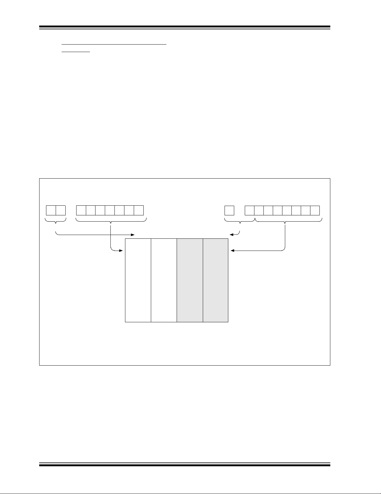
PIC16C62B/72A
Note 1: Maintain clear for upward compatibility with future products.
2: Not implemented.
Data
Memory
Indirect AddressingDirect Addressing
bank select location select
RP1:RP0 6
0
from opcode
IRP FSR register
7
0
bank select
location select
00 01 10 11
Bank 0 Bank 1 Bank 2 Bank 3
not used
FFh
80h
7Fh
00h
17Fh
100h
1FFh
180h
(1)
(1)
(2) (2)
2.5 Indirect Addressing, INDF and FSR
Registers
The INDF register is not a physical register. Addressing INDF actually addresses the register whose
address is contained in the FSR register (FSR is a
pointer
).
Reading INDF itself indirectly (FSR = 0) will produce
00h. Writing to the INDF register indirectly results in a
no-operation (although STATUS bits may be affected).
A simple program to clear RAM locations 20h-2Fh
using indirect addressing is shown in Example 2-1.
FIGURE 2-3: DIRECT/INDIRECT ADDRESSING
EXAMPLE 2-1: HOW TO CLEAR RAM
USING INDIRECT
ADDRESSING
movlw 0x20 ;initialize pointer
movwf FSR ; to RAM
NEXT clrf INDF ;clear INDF register
incf FSR ;inc pointer
btfss FSR,4 ;all done?
goto NEXT ;NO, clear next
CONTINUE
: ;YES, continue
An effective 9-bit address is obtained by concatenating
the 8-bit FSR register and the IRP bit (STATUS<7>), as
shown in Figure 2-3. However, IRP is not used in the
PIC16C62B/72A.
DS35008C-page 18 Preliminary 1998-2013 Microchip Technology Inc.
Page 19
PIC16C62B/72A
Data
Bus
QD
Q
CK
QD
Q
CK
QD
EN
P
N
WR
Por t
WR
TRIS
Data Latch
TRIS Latch
RD TRIS
RD PORT
V
SS
VDD
I/O pin
(1)
Note 1: I/O pins have protection diodes to VDD and
V
SS.
Analog
input
mode
TTL
input
buffer
To A/D Converter (72A only)
(72A
only)
Data
Bus
WR
PORT
WR
TRIS
RD PORT
Data Latch
TRIS Latch
RD TRIS
Schmitt
Trigger
input
buffer
N
V
SS
I/O pin
(1)
TMR0 clock input
QD
Q
CK
QD
Q
CK
EN
QD
EN
Note 1: I/O pin has protection diodes to VSS only.
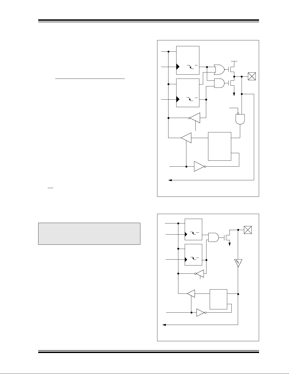
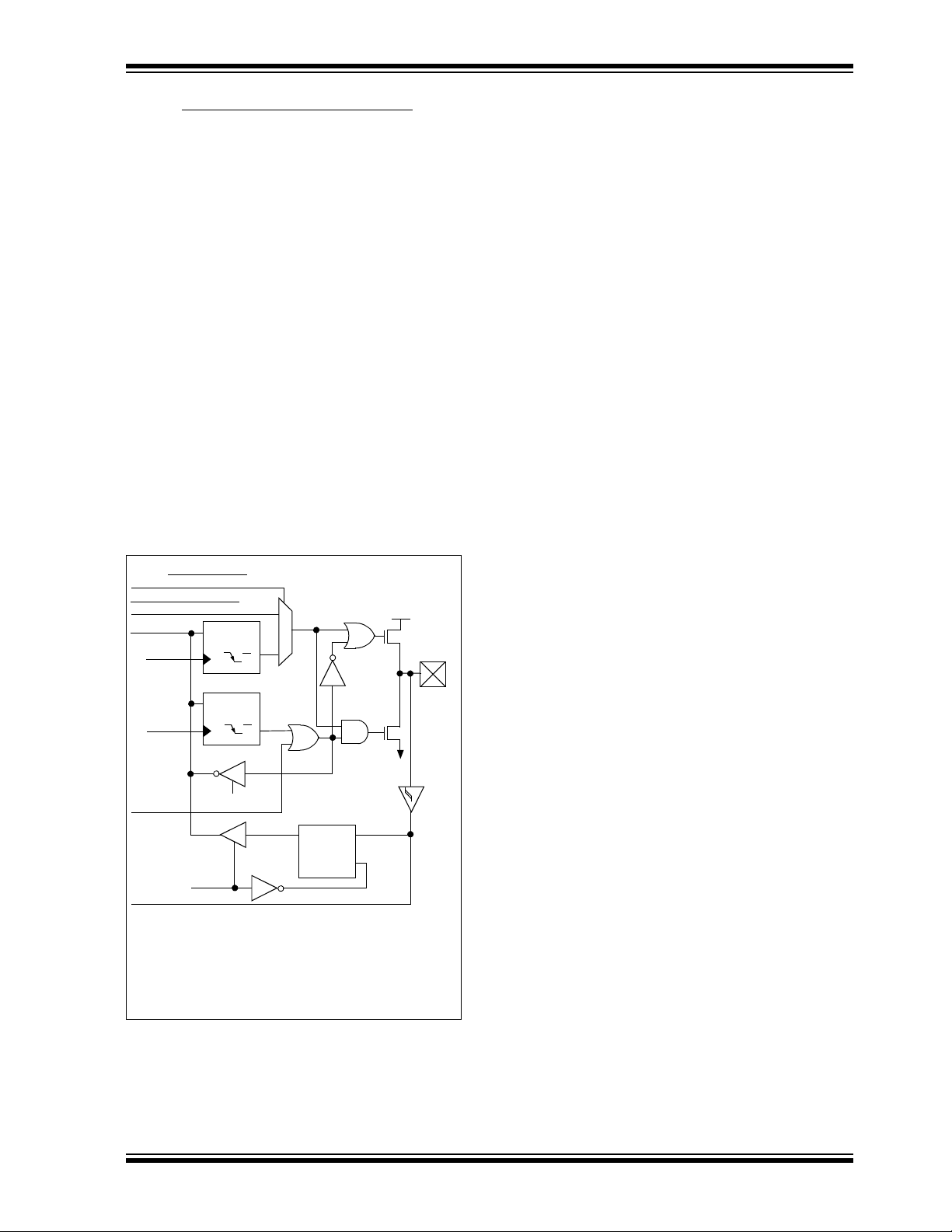
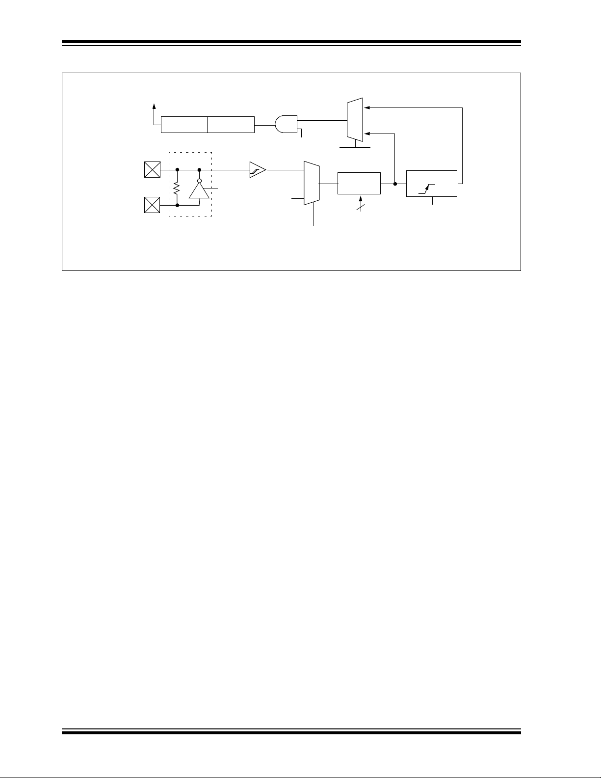
3.0 I/O PORTS
Some I/O port pins are multiplexed with an alternate
function for the peripheral features on the device. In
general, when a peripheral is enabled, that pin may not
be used as a general purpose I/O pin.
Additional information on I/O ports may be found in the
®
MCU Mid-Range Reference Manual, (DS33023).
PIC
3.1 PORTA and the TRISA Register
PORTA is a 6-bit wide bi-directional port. The corresponding data direction register is TRISA. Setting a
TRISA bit (=1) will make the corresponding PORTA pin
an input, i.e., put the corresponding output driver in a
hi-impedance mode. Clearing a TRISA bit (=0) will
make the corresponding PORTA pin an output, (i.e., put
the contents of the output latch on the selected pin).
The PORTA register reads the state of the pins,
whereas writing to it will write to the port latch. All write
operations are read-modify-write operations. Therefore, a write to a port implies that the port pins are read,
this value is modified, and then written to the port data
latch.
Pin RA4 is multiplexed with the Timer0 module clock
input to become the RA4/T0CKI pin. The RA4/T0CKI
pin is a Schmitt Trigger input and an open drain output.
All other RA port pins have TTL input levels and full
CMOS output drivers.
Pin RA5 is multiplexed with the SSP to become the
RA5/SS
On the PIC16C72A device, other PORTA pins are multiplexed with analog inputs and analog VREF input. The
operation of each pin is selected by clearing/setting the
control bits in the ADCON1 register (A/D Control
Register1).
The TRISA register controls the direction of the RA
pins, even when they are being used as analog inputs.
The user must ensure the bits in the TRISA register are
maintained set when using them as analog inputs.
pin.
Note: On a Power-on Reset, pins with analog
functions are configured as analog inputs
with digital input buffers disabled . A digital
read of these pins will return ’0’.
FIGURE 3-1: BLOCK DIAGRAM OF
RA3:RA0 AND RA5 PINS
FIGURE 3-2: BLOCK DIAGRAM OF
RA4/T0CKI PIN
1998-2013 Microchip Technology Inc. Preliminary DS35008C-page 19
Page 20
PIC16C62B/72A
TABLE 3-1 PORTA FUNCTIONS
Name Bit# Buffer Function
RA0/AN0 bit0 TTL Input/output or analog input
RA1/AN1 bit1 TTL Input/output or analog input
RA2/AN2 bit2 TTL Input/output or analog input
RA3/AN3/VREF bit3 TTL Input/output or analog input
Input/output or external clock input for Timer0
RA4/T0CKI bit4 ST
Output is open drain type
RA5/SS/AN4 bit5 TTL Input/output or slave select input for synchronous serial port or analog input
Legend: TTL = TTL input, ST = Schmitt Trigger input
Note 1: The PIC16C62B does not implement the A/D module.
TABLE 3-2 SUMMARY OF REGISTERS ASSOCIATED WITH PORTA
(1)
(1)
(1)
(1)
or VREF
(1)
(1)
Address Name Bit 7 Bit 6 Bit 5 Bit 4 Bit 3 Bit 2 Bit 1 Bit 0
05h PORTA
(for PIC16C72A only)
05h PORTA
(for PIC16C62B only)
85h TRISA
9Fh ADCON1
(1)
— — RA5 RA4 RA3 RA2 RA1 RA0 --0x 0000 --0u 0000
— — RA5 RA4 RA3 RA2 RA1 RA0 --xx xxxx --uu uuuu
— — PORTA Data Direction Register --11 1111 --11 1111
— — — — —PCFG2PCFG1PCFG0---- -000 ---- -000
Value on
POR,
BOR
Value on all
other resets
Legend: x = unknown, u = unchanged, - = unimplemented locations read as '0'. Shaded cells are not used by PORTA.
Note 1: The PIC16C62B does not implement the A/D module. Maintain this register clear.
DS35008C-page 20 Preliminary 1998-2013 Microchip Technology Inc.
Page 21
PIC16C62B/72A
Data Latch
RBPU
(2)
P
V
DD
QD
CK
QD
CK
QD
EN
Data Bus
WR Port
WR TRIS
RD TRIS
RD Port
weak
pull-up
RD Port
RB0/INT
I/O
pin
(1)
TTL
Input
Buffer
Note 1: I/O pins have diode protection to V
DD and VSS.
2: To enable weak pull-ups, set the appropriate TRIS bit(s)
and clear the RBPU
bit (OPTION_REG<7>).
Schmitt Trigger
Buffer
TRIS Latch
Data Latch
From other
RBPU
(2)
P
V
DD
I/O
QD
CK
QD
CK
QD
EN
QD
EN
Data Bus
WR Port
WR TRIS
Set RBIF
TRIS Latch
RD TRIS
RD Port
RB7:RB4 pins
weak
pull-up
RD Port
Latch
TTL
Input
Buffer
pin
(1)
Note 1: I/O pins have diode protection to VDD and VSS.
ST
Buffer
RB7:RB6 in serial programming mode
Q3
Q1
2: To enable weak pull-ups, set the appropriate TRIS bit(s)
and clear the RBPU
bit (OPTION_REG<7>).
3.2 PORTB and the TRISB Register
PORTB is an 8-bit wide bi-directional port. The corresponding data direction register is TRISB. Setting a
TRISB bit (=1) will make the corresponding PORTB pin
an input, (i.e., put the corresponding output driver in a
hi-impedance mode). Clearing a TRISB bit (=0) will
make the corresponding PORTB pin an output, (i.e.,
put the contents of the output latch on the selected pin).
Each of the PORTB pins has a weak internal pull-up. A
single control bit can turn on all the pull-ups. This is performed by clearing bit RBPU
(OPTION_REG<7>). The
weak pull-up is automatically turned off when the port
pin is configured as an output. The pull-ups are disabled on a Power-on Reset.
FIGURE 3-3: BLOCK DIAGRAM OF
RB3:RB0 PINS
Four of PORTB’s pins, RB7:RB4, have an interrupt on
change feature. Only pins configured as inputs can
cause this interrupt to occur (i.e. any RB7:RB4 pin configured as an output is excluded from the interrupt on
change comparison). The input pins (of RB7:RB4) are
compared with the old value latched on the last read of
PORTB. The “mismatch” outputs of RB7:RB4 are
OR’ed together to generate the RB Port Change Interrupt with flag bit RBIF (INTCON<0>).
This interrupt can wake the device from SLEEP. The
user, in the interrupt service routine, can clear the interrupt in the following manner:
a) Any read or write of PORTB. This will end the
mismatch condition.
b) Clear flag bit RBIF.
A mismatch condition will continue to set flag bit RBIF.
Reading PORTB will end the mismatch condition and
allow flag bit RBIF to be cleared.
The interrupt on change feature is recommended for
wake-up on key depression operation and operations
where PORTB is only used for the interrupt on change
feature. Polling of PORTB is not recommended while
using the interrupt on change feature.
RB0/INT is an external interupt pin and is configured
using the INTEDG bit (OPTION_REG<6>). RB0/INT is
discussed in detail in Section 10.10.1.
1998-2013 Microchip Technology Inc. Preliminary DS35008C-page 21
FIGURE 3-4: BLOCK DIAGRAM OF
RB7:RB4 PINS
Page 22
PIC16C62B/72A
TABLE 3-3 PORTB FUNCTIONS
Name Bit# Buffer Function
RB0/INT bit0 TTL/ST
RB1 bit1 TTL Input/output pin. Internal software programmable weak pull-up.
RB2 bit2 TTL Input/output pin. Internal software programmable weak pull-up.
RB3 bit3 TTL Input/output pin. Internal software programmable weak pull-up.
RB4 bit4 TTL Input/output pin (with interrupt on change).
RB5 bit5 TTL Input/output pin (with interrupt on change).
RB6 bit6 TTL/ST
RB7 bit7 TTL/ST
Legend: TTL = TTL input, ST = Schmitt Trigger input
Note 1: This buffer is a Schmitt Trigger input when configured as the external interrupt.
2: This buffer is a Schmitt Trigger input when used in serial programming mode.
TABLE 3-4 SUMMARY OF REGISTERS ASSOCIATED WITH PORTB
(1)
Input/output pin or external interrupt input.
Internal software programmable weak pull-up.
Internal software programmable weak pull-up.
Internal software programmable weak pull-up.
(2)
Input/output pin (with interrupt on change).
Internal software programmable weak pull-up. Serial programming clock.
(2)
Input/output pin (with interrupt on change).
Internal software programmable weak pull-up. Serial programming data.
Address Name Bit 7 Bit 6 Bit 5 Bit 4 Bit 3 Bit 2 Bit 1 Bit 0
06h PORTB RB7 RB6 RB5 RB4 RB3 RB2 RB1 RB0 xxxx xxxx uuuu uuuu
86h TRISB PORTB Data Direction Register 1111 1111 1111 1111
81h OPTION_REG RBPU
Legend: x = unknown, u = unchanged. Shaded cells are not used by PORTB.
INTEDG T0CS T0SE PSA PS2 PS1 PS0 1111 1111 1111 1111
Value on:
POR,
BOR
Value on all
other resets
DS35008C-page 22 Preliminary 1998-2013 Microchip Technology Inc.
Page 23
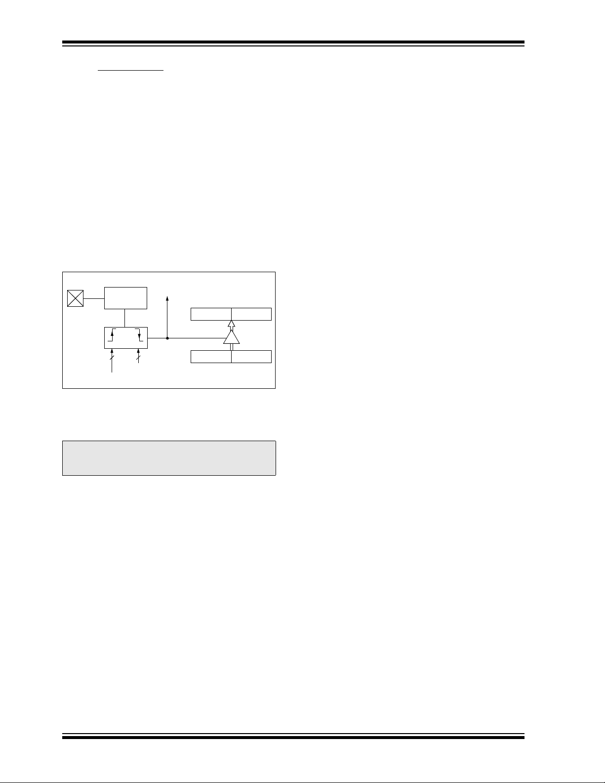
3.3 PORTC and the TRISC Register
PORT/PERIPHERAL Select
(2)
Data Bus
WR
PORT
WR
TRIS
RD
Data Latch
TRIS Latch
RD TRIS
Schmitt
Trigger
QD
Q
CK
QD
EN
Peripheral Data Out
0
1
QD
Q
CK
P
N
V
DD
VSS
PORT
Peripheral
OE
(3)
Peripheral input
I/O
pin
(1)
Note 1: I/O pins have diode protection to VDD and VSS.
2: Port/Peripheral select signal selects between port
data and peripheral output.
3: Peripheral OE (output enable) is only activated if
peripheral select is active.
PORTC is an 8-bit wide bi-directional port. The corresponding data direction register is TRISC. Setting a
TRISC bit (=1) will make the corresponding PORTC pin
an input, (i.e., put the corresponding output driver in a
hi-impedance mode). Clearing a TRISC bit (=0) will
make the corresponding PORTC pin an output, (i.e.,
put the contents of the output latch on the selected pin).
PORTC is multiplexed with several peripheral functions
(Table 3-5). PORTC pins have Schmitt Trigger input
buffers.
When enabling peripheral functions, care should be
taken in defining TRIS bits for each PORTC pin. Some
peripherals override the TRIS bit to make a pin an output, while other peripherals override the TRIS bit to
make a pin an input. Since the TRIS bit override maybe
in effect while the peripheral is enabled, read-modifywrite instructions (BSF, BCF, XORWF) with TRISC as
destination should be avoided. The user should refer to
the corresponding peripheral section for the correct
TRIS bit settings.
PIC16C62B/72A
FIGURE 3-5: PORTC BLOCK DIAGRAM
(PERIPHERAL OUTPUT
OVERRIDE)
1998-2013 Microchip Technology Inc. Preliminary DS35008C-page 23
Page 24
PIC16C62B/72A
TABLE 3-5 PORTC FUNCTIONS
bit0
Buffer
Function
Typ e
ST Input/output port pin or Timer1 oscillator output/Timer1 clock input Yes
output
RC3 can also be the synchronous serial clock for both SPI and I
modes.
2
RC4 can also be the SPI Data In (SPI mode) or data I/O (I
C mode).
Name Bit#
RC0/T1OSO/T1CKI
RC1/T1OSI bit1 ST Input/output port pin or Timer1 oscillator input Yes
RC2/CCP1 bit2 ST Input/output port pin or Capture1 input/Compare1 output/PWM1
RC3/SCK/SCL bit3 ST
RC4/SDI/SDA bit4 ST
RC5/SDO bit5 ST Input/output port pin or Synchronous Serial Port data output No
RC6 bit6 ST Input/output port pin No
RC7 bit7 ST Input/output port pin No
Legend: ST = Schmitt Trigger input
2
C
TRISC
Override
No
No
No
TABLE 3-6 SUMMARY OF REGISTERS ASSOCIATED WITH PORTC
Value on:
Address Name Bit 7 Bit 6 Bit 5 Bit 4 Bit 3 Bit 2 Bit 1 Bit 0
07h PORTC RC7 RC6 RC5 RC4 RC3 RC2 RC1 RC0 xxxx xxxx uuuu uuuu
87h TRISC PORTC Data Direction Register 1111 1111 1111 1111
Legend: x = unknown, u = unchanged.
POR,
BOR
Value on all
other resets
DS35008C-page 24 Preliminary 1998-2013 Microchip Technology Inc.
Page 25
PIC16C62B/72A
Note 1: T0CS, T0SE, PSA, PS2:PS0 (OPTION_REG<5:0>).
2: The prescaler is shared with Watchdog Timer (refer to Figure 4-2 for detailed block diagram).
RA4/T0CKI
T0SE
0
1
1
0
pin
T0CS
FOSC/4
Programmable
Prescaler
Sync with
Internal
clocks
TMR0
PSout
(T
CY delay)
PSout
Data Bus
8
PSA
PS2, PS1, PS0
Set interrupt
flag bit T0IF
on overflow
3
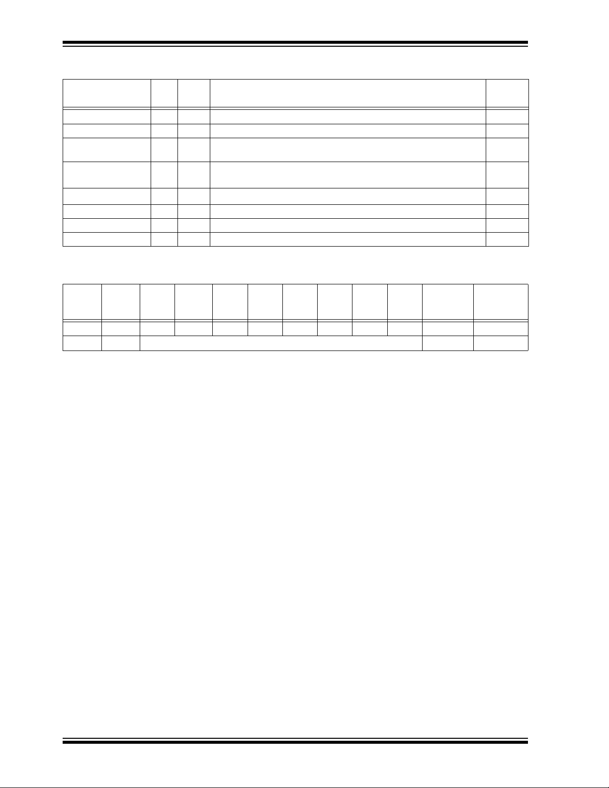
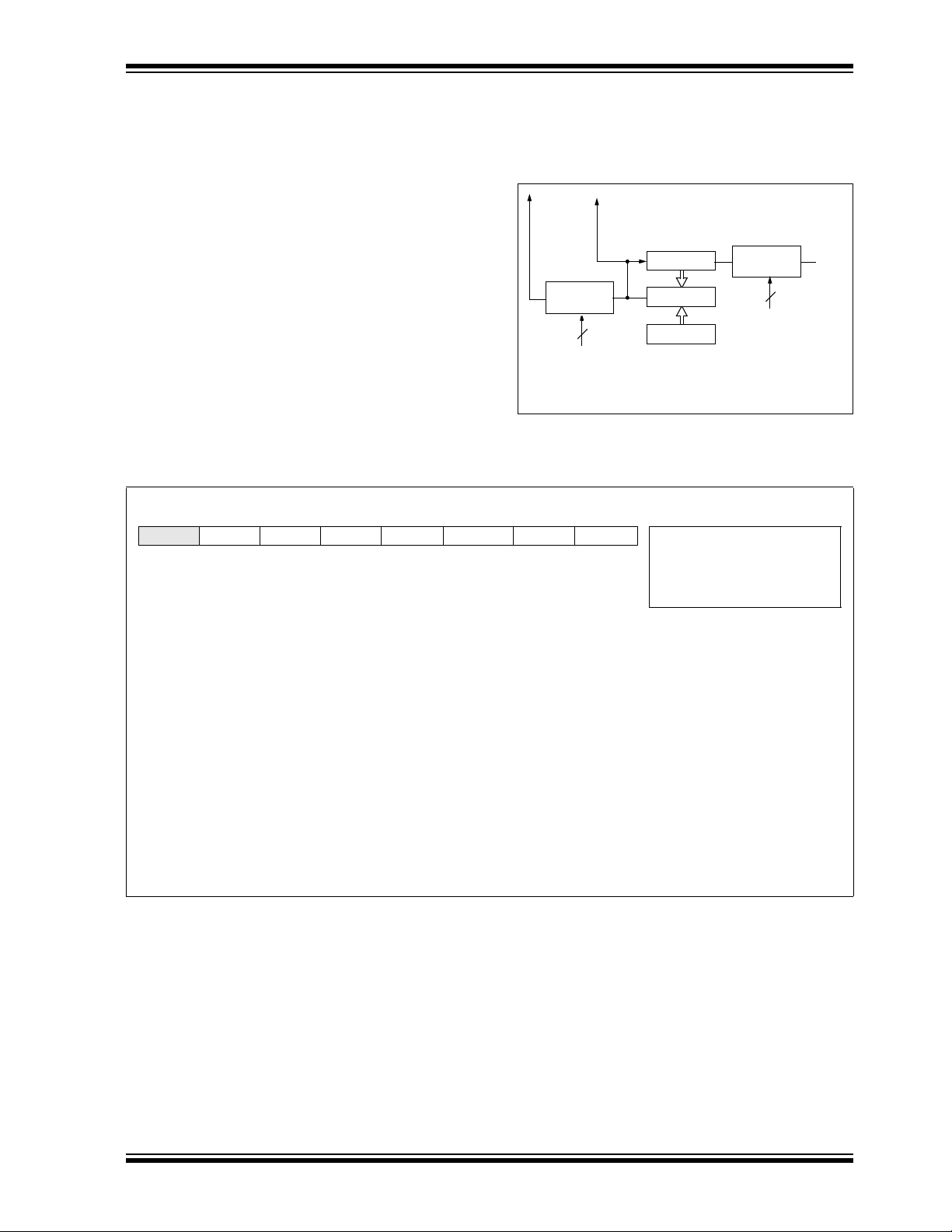
4.0 TIMER0 MODULE
The Timer0 module timer/counter has the following features:
• 8-bit timer/counter
- Read and write
- INT on overflow
• 8-bit software programmable prescaler
• INT or EXT clock select
- EXT clock edge select
Figure 4-1 is a simplified block diagram of the Timer0
module.
Additional information on timer modules is available in
the PIC
(DS33023).
4.1 Timer0 Operation
Timer0 can operate as a timer or as a counter.
Timer mode is selected by clearing bit T0CS
(OPTION_REG<5>). In timer mode, the Timer0 module will increment every instruction cycle (without prescaler). If the TMR0 register is written, the increment is
inhibited for the following two instruction cycles. The
user can work around this by writing an adjusted value
to the TMR0 register.
Counter mode is selected by setting bit T0CS
(OPTION_REG<5>). In counter mode, Timer0 will
increment either on every rising or falling edge of pin
RA4/T0CKI. The incrementing edge is determined by
the Timer0 Source Edge Select bit T0SE
(OPTION_REG<4>). Clearing bit T0SE selects the rising edge. Restrictions on the external clock input are
discussed below.
When an external clock input is used for Timer0, it must
meet certain requirements. The requirements ensure
the external clock can be synchronized with the internal
phase clock (T
incrementing of Timer0 after synchronization.
®
MCU Mid-Range Reference Manual,
OSC). Also, there is a delay in the actual
Additional information on external clock requirements
is available in the Electrical Specifications section of
this manual, and in the PIC
®
MCU Mid-Range Refer-
ence Manual, (DS33023).
4.2 Prescaler
An 8-bit counter is available as a prescaler for the
Timer0 module, or as a postscaler for the Watchdog
Timer, respectively (Figure 4-2). For simplicity, this
counter is being referred to as “prescaler” throughout
this data sheet. There is only one prescaler available
which is shared between the Timer0 module and the
Watchdog Timer. A prescaler assignment for the
Timer0 module means that there is no prescaler for the
Watchdog Timer, and vice-versa.
The prescaler is not readable or writable.
The PSA and PS2:PS0 bits (OPTION_REG<3:0>)
determine the prescaler assignment and prescale ratio.
Clearing bit PSA will assign the prescaler to the Timer0
module. When the prescaler is assigned to the Timer0
module, prescale values of 1:2, 1:4, ..., 1:256 are
selectable.
Setting bit PSA will assign the prescaler to the Watchdog Timer (WDT). When the prescaler is assigned to
the WDT, prescale values of 1:1, 1:2, ..., 1:128 are
selectable.
When assigned to the Timer0 module, all instructions
writing to the TMR0 register (e.g. CLRF 1, MOVWF 1,
BSF 1,x....etc.) will clear the prescaler. When
assigned to WDT, a CLRWDT instruction will clear the
prescaler along with the WDT.
Note: Writing to TMR0 when the prescaler is
assigned to Timer0 will clear the prescaler
count, but will not change the prescaler
assignment or ratio.
FIGURE 4-1: TIMER0 BLOCK DIAGRAM
1998-2013 Microchip Technology Inc. Preliminary DS35008C-page 25
Page 26
PIC16C62B/72A
RA4/T0CKI
T0SE
pin
M
U
X
CLKOUT (= Fosc/4)
SYNC
2
T
CY
TMR0 reg
8-bit Prescaler
8 - to - 1MUX
M
U
X
M U X
Watchdog
Timer
PSA
0
1
0
1
WDT
Time-out
PS2:PS0
8
Note: T0CS, T0SE, PSA, PS2:PS0 are (OPTION_REG<5:0>).
PSA
WDT Enable bit
M
U
X
0
1
0
1
Data Bus
Set flag bit T0IF
on Overflow
8
PSA
T0CS
Prescaler
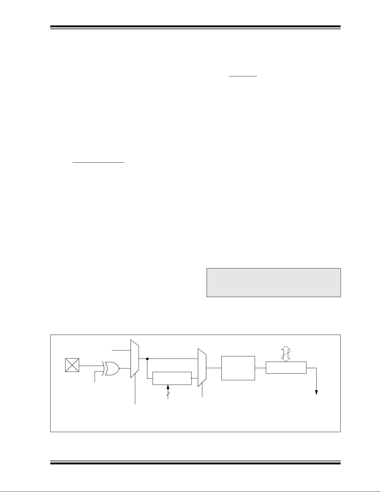
4.2.1 SWITCHING PRESCALER ASSIGNMENT
The prescaler assignment is fully under software control, (i.e., it can be changed “on-the-fly” during program
execution).
Note: To avoid an unintended device RESET, a
specific instruction sequence (shown in the
®
MCU Mid-Range Reference Manual,
PIC
DS33023) must be executed when changing the prescaler assignment from Timer0
4.3 Timer0 Interrupt
The TMR0 interrupt is generated when the TMR0 register overflows from FFh to 00h. This overflow sets bit
T0IF (INTCON<2>). The interrupt can be masked by
clearing bit T0IE (INTCON<5>). Bit T0IF must be
cleared in software by the Timer0 module interrupt service routine before re-enabling this interrupt. The
TMR0 interrupt cannot awaken the processor from
SLEEP since the timer is shut off during SLEEP.
to the WDT. This sequence must be followed even if the WDT is disabled.
FIGURE 4-2: BLOCK DIAGRAM OF THE TIMER0/WDT PRESCALER
TABLE 4-1 REGISTERS ASSOCIATED WITH TIMER0
Address Name Bit 7 Bit 6 Bit 5 Bit 4 Bit 3 Bit 2 Bit 1 Bit 0
01h TMR0 Timer0 module’s register xxxx xxxx uuuu uuuu
0Bh,8Bh INTCON GIE
81h OPTION_REG
85h TRISA
Legend: x = unknown, u = unchanged, - = unimplemented locations read as '0'. Shaded cells are not used by Timer0.
DS35008C-page 26 Preliminary 1998-2013 Microchip Technology Inc.
RBPU INTEDG T0CS T0SE PSA PS2 PS1 PS0 1111 1111 1111 1111
— — PORTA Data Direction Register --11 1111 --11 1111
PEIE T0IE INTE RBIE T0IF INTF RBIF 0000 000x 0000 000u
Val ue o n:
POR,
BOR
Value on all
other resets
Page 27

PIC16C62B/72A
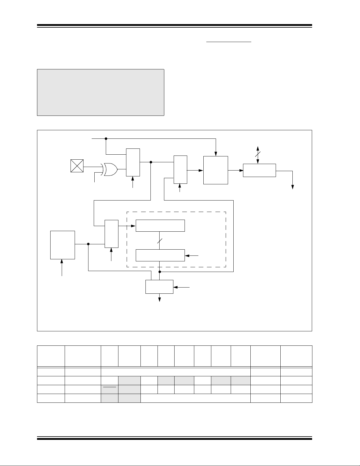
5.0 TIMER1 MODULE
The Timer1 module timer/counter has the following features:
• 16-bit timer/counter
• Readable and writable
• Internal or external clock select
• Interrupt on overflow from FFFFh to 0000h
• Reset from CCP module trigger
Timer1 has a control register, shown in Register 5-1.
Timer1 can be enabled/disabled by setting/clearing
control bit TMR1ON (T1CON<0>).
Figure 5-1 is a simplified block diagram of the Timer1
module.
Additional information on timer modules is available in
the PIC
(DS33023).
®
MCU Mid-Range Reference Manual,
5.1 Timer1 Operation
Timer1 can operate in one of these modes:
•As a timer
• As a synchronous counter
• As an asynchronous counter
The operating mode is determined by the clock select
bit, TMR1CS (T1CON<1>).
In timer mode, Timer1 increments every instruction
cycle. In counter mode, it increments on every rising
edge of the external clock input.
When the Timer1 oscillator is enabled (T1OSCEN is
set), the RC1/T1OSI and RC0/T1OSO/T1CKI pins
become inputs. That is, the TRISC<1:0> value is
ignored.
Timer1 also has an internal “reset input”. This reset can
be generated by the CCP module as a special event
trigger (Section 7.0).
REGISTER 5-1:T1CON: TIMER1 CONTROL REGISTER (ADDRESS 10h)
U-0 U-0 R/W-0 R/W-0 R/W-0 R/W-0 R/W-0 R/W-0
— — T1CKPS1 T1CKPS0 T1OSCEN T1SYNC TMR1CS TMR1ON
bit7 bit0
bit 7-6: Unimplemented: Read as '0'
bit 5-4: T1CKPS1:T1CKPS0: Timer1 Input Clock Prescale Select bits
11 = 1:8 Prescale value
10 = 1:4 Prescale value
01 = 1:2 Prescale value
00 = 1:1 Prescale value
bit 3: T1OSCEN: Timer1 Oscillator Enable Control bit
1 = Oscillator is enabled (TRISC<1:0> ignored)
0 = Oscillator is shut off
(The oscillator is turned off to reduce power drain
bit 2: T1SYNC
T
1 = Do not synchronize external clock input
0 = Synchronize external clock input
T
This bit is ignored. Timer1 uses the internal clock when TMR1CS = 0.
bit 1: TMR1CS: Timer1 Clock Source Select bit
1 = External clock from pin RC0/T1OSO/T1CKI (on the rising edge)
0 = Internal clock (F
bit 0: TMR1ON: Timer1 On bit
1 = Enables Timer1
0 = Stops Timer1
: Timer1 External Clock Input Synchronization Control bit
MR1CS = 1
MR1CS = 0
OSC/4)
R = Readable bit
W = Writable bit
U = Unimplemented bit,
read as ‘0’
- n = Value at POR reset
1998-2013 Microchip Technology Inc. Preliminary DS35008C-page 27
Page 28
PIC16C62B/72A
TMR1H
TMR1L
T1OSC
T1SYNC
TMR1CS
T1CKPS1:T1CKPS0
SLEEP input
T1OSCEN
Enable
Oscillator
(1)
FOSC/4
Internal
Clock
TMR1ON
on/off
Prescaler
1, 2, 4, 8
Synchronize
det
1
0
0
1
Synchronized
clock input
2
RC0/T1OSO/T1CKI
RC1/T1OSI
Note 1: When the T1OSCEN bit is cleared, the inverter and feedback resistor are turned off. This eliminates power drain.
Set flag bit
TMR1IF on
Overflow
TMR1
FIGURE 5-1: TIMER1 BLOCK DIAGRAM
DS35008C-page 28 Preliminary 1998-2013 Microchip Technology Inc.
Page 29
PIC16C62B/72A
5.2 Timer1 Oscillator
A crystal oscillator circuit is built-in between pins T1OSI
(input) and T1OSO (amplifier output). It is enabled by
setting control bit T1OSCEN (T1CON<3>). When the
Timer1 oscillator is enabled, RC0 and RC1 pins
become T1OSO and T1OSI inputs, overriding
TRISC<1:0>.
The oscillator is a low power oscillator rated up to 200
kHz. It will continue to run during SLEEP. It is primarily
intended for a 32 kHz crystal. Table 5-1 shows the
capacitor selection for the Timer1 oscillator.
The Timer1 oscillator is identical to the LP oscillator.
The user must provide a software time delay to ensure
proper oscillator start-up.
TABLE 5-1 CAPACITOR SELECTION FOR
THE TIMER1 OSCILLATOR
Osc Type Freq C1 C2
LP 32 kHz 33 pF 33 pF
100 kHz 15 pF 15 pF
200 kHz 15 pF 15 pF
These values are for design guidance only.
Crystals Tested:
32.768 kHz Epson C-001R32.768K-A 20 PPM
100 kHz Epson C-2 100.00 KC-P 20 PPM
200 kHz STD XTL 200.000 kHz 20 PPM
Note 1: Higher capacitance increases the stability
of oscillator but also increases the start-up
time.
2: Since each resonator/crystal has its own
characteristics, the user should consult the
resonator/crystal manufacturer for appropriate values of external components.
5.3 Timer1 Interrupt
The TMR1 Register pair (TMR1H:TMR1L) increments
from 0000h to FFFFh and rolls over to 0000h. The
TMR1 Interrupt, if enabled, is generated on overflow
and is latched in interrupt flag bit TMR1IF (PIR1<0>).
This interrupt can be enabled by setting TMR1 interrupt
enable bit TMR1IE (PIE1<0>).
5.4 Resetting Timer1 using a CCP Trigger
Output
If the CCP module is configured in compare mode to
generate a “special event trigger" (CCP1M3:CCP1M0
= 1011), this signal will reset Timer1 and start an A/D
conversion (if the A/D module is enabled).
Note: The special event trigger from the CCP1
module will not set interrupt flag bit
TMR1IF (PIR1<0>).
Timer1 must be configured for either timer or synchronized counter mode to take advantage of this feature. If
Timer1 is running in asynchronous counter mode, this
reset operation may not work.
In the event that a write to Timer1 coincides with a special event trigger from CCP1, the write will take precedence.
In this mode of operation, the CCPR1H:CCPR1L registers pair effectively becomes the period register for
Timer1.
TABLE 5-2 REGISTERS ASSOCIATED WITH TIMER1 AS A TIMER/COUNTER
Address Name Bit 7 Bit 6 Bit 5 Bit 4 Bit 3 Bit 2 Bit 1 Bit 0
0Bh,8Bh INTCON GIE PEIE
0Ch PIR1
8Ch PIE1
0Eh TMR1L Holding register for the Least Significant Byte of the 16-bit TMR1 register
0Fh TMR1H Holding register for the Most Significant Byte of the 16-bit TMR1 register
10h T1CON
Legend: x = unknown, u = unchanged, - = unimplemented read as '0'. Shaded cells are not used by the Timer1 module.
1998-2013 Microchip Technology Inc. Preliminary DS35008C-page 29
— ADIF — — SSPIF CCP1IF TMR2IF TMR1IF
— ADIE — — SSPIE CCP1IE TMR2IE TMR1IE
— — T1CKPS1 T1CKPS0 T1OSCEN T1SYNC TMR1CS TMR1ON
T0IE INTE RBIE T0IF INTF RBIF
Value on
POR,
BOR
0000 000x 0000 000u
-0-- 0000 -0-- 0000
-0-- 0000 -0-- 0000
xxxx xxxx uuuu uuuu
xxxx xxxx uuuu uuuu
--00 0000 --uu uuuu
Value on
all other
resets
Page 30

PIC16C62B/72A
NOTES:
DS35008C-page 30 Preliminary 1998-2013 Microchip Technology Inc.
Page 31
PIC16C62B/72A
Comparator
TMR2
Sets flag
TMR2 reg
output
(1)
Reset
Postscaler
Prescaler
PR2 reg
2
F
OSC/4
1:1 1:16
1:1, 1:4, 1:16
EQ
4
bit TMR2IF
Note 1: TMR2 register output can be software selected
by the SSP Module as a baud clock.
to
6.0 TIMER2 MODULE
The Timer2 module timer has the following features:
Additional information on timer modules is available in
the PIC
®
MCU Mid-Range Reference Manual,
(DS33023).
• 8-bit timer (TMR2 register)
- Readable and writable
FIGURE 6-1: TIMER2 BLOCK DIAGRAM
• 8-bit period register (PR2)
- Readable and writable
• Software programmable prescaler (1:1, 1:4, 1:16)
• Software programmable postscaler (1:1 to 1:16)
• Interrupt on match (TMR2 = PR2)
• Timer2 can be used by SSP and CCP
Timer2 has a control register, shown in Register 6-1.
Timer2 can be shut off by clearing control bit TMR2ON
(T2CON<2>) to minimize power consumption.
Figure 6-1 is a simplified block diagram of the Timer2
module.
REGISTER 6-1:T2CON: TIMER2 CONTROL REGISTER (ADDRESS 12h)
U-0 R/W-0 R/W-0 R/W-0 R/W-0 R/W-0 R/W-0 R/W-0
— TOUTPS3 TOUTPS2 TOUTPS1 TOUTPS0 TMR2ON T2CKPS1 T2CKPS0 R = Readable bit
bit7 bit0
bit 7: Unimplemented: Read as '0'
bit 6-3: TOUTPS3:TOUTPS0: Timer2 Output Postscale Select bits
0000 = 1:1 Postscale
0001 = 1:2 Postscale
0010 = 1:3 Postscale
•
•
•
1111 = 1:16 Postscale
bit 2: TMR2ON: Timer2 On bit
1 = Timer2 is on
0 = Timer2 is off
bit 1-0: T2CKPS1:T2CKPS0: Timer2 Clock Prescale Select bits
00 = Prescaler is 1
01 = Prescaler is 4
1x = Prescaler is 16
W = Writable bit
U = Unimplemented bit,
- n = Value at POR reset
read as ‘0’
1998-2013 Microchip Technology Inc. Preliminary DS35008C-page 31
Page 32

PIC16C62B/72A
6.1 Timer2 Operation
The Timer2 output is also used by the CCP module to
generate the PWM "On-Time", and the PWM period
with a match with PR2.
The TMR2 register is readable and writable, and is
cleared on any device reset.
The input clock (F
OSC/4) has a prescale option of 1:1,
6.2 Timer2 Interrupt
The Timer2 module has an 8-bit period register PR2.
Timer2 increments from 00h until it matches PR2 and
then resets to 00h on the next increment cycle. PR2 is
a readable and writable register. The PR2 register is initialized to FFh upon reset.
6.3 Output of TMR2
1:4 or 1:16, selected by control bits
T2CKPS1:T2CKPS0 (T2CON<1:0>).
The match output of TMR2 goes through a 4-bit postscaler (which gives a 1:1 to 1:16 scaling) to generate a
The output of TMR2 (before the postscaler) is fed to the
Synchronous Serial Port module, which optionally uses
it to generate shift clock.
TMR2 interrupt (latched in flag bit TMR2IF, (PIR1<1>)).
The prescaler and postscaler counters are cleared
when any of the following occurs:
• a write to the TMR2 register
• a write to the T2CON register
• any device reset (Power-on Reset, MCLR
reset,
Watchdog Timer reset or Brown-out Reset)
TMR2 is not cleared when T2CON is written.
TABLE 6-1 REGISTERS ASSOCIATED WITH TIMER2 AS A TIMER/COUNTER
Address Name Bit 7 Bit 6 Bit 5 Bit 4 Bit 3 Bit 2 Bit 1 Bit 0
0Bh,8Bh INTCON GIE PEIE
0Ch PIR1
8Ch PIE1
11h TMR2 Timer2 module’s register
12h T2CON
92h PR2 Timer2 Period Register
Legend: x = unknown, u = unchanged, - = unimplemented read as '0'. Shaded cells are not used by the Timer2 module.
— ADIF — — SSPIF CCP1IF TMR2IF TMR1IF
— ADIE — — SSPIE CCP1IE TMR2IE TMR1IE
— TOUTPS3 TOUTPS2 TOUTPS1 TOUTPS0 TMR2ON T2CKPS1 T2CKPS0
T0IE INTE RBIE T0IF INTF RBIF
Val ue on
POR,
BOR
0000 000x 0000 000u
-00- 0000 0000 0000
-0-- 0000 0000 0000
0000 0000 0000 0000
-000 0000 -000 0000
1111 1111 1111 1111
Val ue on
all other
resets
DS35008C-page 32 Preliminary 1998-2013 Microchip Technology Inc.
Page 33

PIC16C62B/72A
7.0 CAPTURE/COMPARE/PWM
(CCP) MODULE
The CCP (Capture/Compare/PWM) module contains a
16-bit register, which can operate as a 16-bit capture
register, as a 16-bit compare register or as a PWM
master/slave duty cycle register. Table 7-1 shows the
timer resources of the CCP module modes.
Capture/Compare/PWM Register 1 (CCPR1) is comprised of two 8-bit registers: CCPR1L (low byte) and
CCPR1H (high byte). The CCP1CON register controls
the operation of CCP1. All are readable and writable.
Additional information on the CCP module is available
in the PIC
(DS33023).
®
MCU Mid-Range Reference Manual,
TABLE 7-1 CCP MODE - TIMER
RESOURCE
CCP Mode Timer Resource
Capture
Compare
PWM
Timer1
Timer1
Timer2
TABLE 7-2 INTERACTION OF TWO CCP MODULES
CCPx Mode CCPy Mode Interaction
Capture Capture Same TMR1 time-base.
Capture Compare The compare should be configured for the special event trigger, which clears TMR1.
Compare Compare The compare(s) should be configured for the special event trigger, which clears TMR1.
PWM PWM The PWMs will have the same frequency and update rate (TMR2 interrupt).
PWM Capture None.
PWM Compare None.
REGISTER 7-1:CCP1CON REGISTER (ADDRESS 17h)
U-0 U-0 R/W-0 R/W-0 R/W-0 R/W-0 R/W-0 R/W-0
— — CCP1X CCP1Y CCP1M3 CCP1M2 CCP1M1 CCP1M0 R = Readable bit
bit7 bit0
bit 7-6: Unimplemented: Read as '0'
bit 5-4: CCP1X:CCP1Y: PWM Least Significant bits
Capture Mode: Unused
Compare Mode: Unused
PWM Mode: These bits are the two LSbs of the PWM duty cycle. The eight MSbs are found in CCPR1L.
bit 3-0: CCP1M3:CCP1M0: CCP1 Mode Select bits
0000 = Capture/Compare/PWM off (resets CCP1 module)
0100 = Capture mode, every falling edge
0101 = Capture mode, every rising edge
0110 = Capture mode, every 4th rising edge
0111 = Capture mode, every 16th rising edge
1000 = Compare mode, set output on match (CCP1IF bit is set)
1001 = Compare mode, clear output on match (CCP1IF bit is set)
1010 = Compare mode, generate software interrupt on match (CCP1IF bit is set, CCP1 pin is unaffected)
1011 = Compare mode, trigger special event (CCP1IF bit is set; CCP1 resets TMR1 and starts an A/D
conversion (if A/D module is enabled))
11xx = PWM mode
W = Writable bit
U = Unimplemented bit, read
as ‘0’
- n =Value at POR reset
1998-2013 Microchip Technology Inc. Preliminary DS35008C-page 33
Page 34
PIC16C62B/72A
CCPR1H CCPR1L
TMR1H TMR1L
Set flag bit CCP1IF
(PIR1<2>)
Capture
Enable
Q’s
CCP1CON<3:0>
RC2/CCP1
Prescaler
1, 4, 16
and
edge detect
Pin
7.1 Capture Mode
In Capture mode, CCPR1H:CCPR1L captures the
16-bit value of the TMR1 register, when an event
occurs on pin RC2/CCP1. An event is defined as:
• every falling edge
• every rising edge
• every 4th rising edge
• every 16th rising edge
An event is selected by control bits CCP1M3:CCP1M0
(CCP1CON<3:0>). When a capture is made, the interrupt request flag bit ,CCP1IF (PIR1<2>), is set. It must
be cleared in software. If another capture occurs before
the value in register CCPR1 is read, the old captured
value will be lost.
FIGURE 7-1: CAPTURE MODE OPERATION
BLOCK DIAGRAM
7.1.4 CCP PRESCALER
There are four prescaler settings, specified by bits
CCP1M3:CCP1M0. Whenever the CCP module is
turned off, or the CCP module is not in capture mode,
the prescaler counter is cleared. This means that any
reset will clear the prescaler counter.
Switching from one capture prescaler to another may
generate an interrupt. Also, the prescaler counter will
not be cleared, therefore the first capture may be from
a non-zero prescaler. Example 7-1 shows the recommended method for switching between capture prescalers. This example also clears the prescaler counter
and will not generate the “false” interrupt.
EXAMPLE 7-1: CHANGING BETWEEN
CAPTURE PRESCALERS
CLRF CCP1CON ;Turn CCP module off
MOVLW NEW_CAPT_PS ;Load the W reg with
; the new prescaler
; mode value and CCP ON
MOVWF CCP1CON ;Load CCP1CON with this
; value
7.1.1 CCP PIN CONFIGURATION
In Capture mode, the RC2/CCP1 pin should be configured as an input by setting the TRISC<2> bit.
Note: If the RC2/CCP1 is configured as an out-
put, a write to the port can cause a capture
condition.
7.1.2 TIMER1 MODE SELECTION
Timer1 must be running in timer mode or synchronized
counter mode for the CCP module to use the capture
feature. In asynchronous counter mode, the capture
operation may not work consistently.
7.1.3 SOFTWARE INTERRUPT
When the Capture mode is changed, a false capture
interrupt may be generated. The user should clear
CCP1IE (PIE1<2>) before changing the capture mode
to avoid false interrupts. Clear the interrupt flag bit,
CCP1IE before setting CCP1IE.
DS35008C-page 34 Preliminary 1998-2013 Microchip Technology Inc.
Page 35

PIC16C62B/72A
CCPR1H CCPR1L
TMR1H TMR1L
Comparator
QS
R
Output
Logic
Special Event Trigger
Set flag bit CCP1IF
(PIR1<2>)
match
RC2/CCP1
TRISC<2>
CCP1CON<3:0>
Mode Select
Output Enable
Pin
Special event trigger will:
reset Timer1, but not set interrupt flag bit TMR1IF (PIR1<0>),
and set bit GO/DONE
(ADCON0<2>), which starts an A/D
conversion
7.2 Compare Mode
In Compare mode, the 16-bit CCPR1 register value is
constantly compared against the TMR1 register pair
value. When a match occurs, the RC2/CCP1 pin is:
•driven High
• driven Low
• remains Unchanged
The action on the pin is based on the value of control
bits CCP1M3:CCP1M0 (CCP1CON<3:0>). The interrupt flag bit, CCP1IF, is set on all compare matches.
FIGURE 7-2: COMPARE MODE
OPERATION BLOCK
DIAGRAM
7.2.1 CCP PIN CONFIGURATION
The user must configure the RC2/CCP1 pin as an output by clearing the TRISC<2> bit.
Note: Clearing the CCP1CON register will force
the RC2/CCP1 compare output latch to the
default low level. This is not the data latch.
7.2.2 TIMER1 MODE SELECTION
Timer1 must be running in Timer mode or Synchronized Counter mode if the CCP module is using the
compare feature. In Asynchronous Counter mode, the
compare operation may not work.
7.2.3 SOFTWARE INTERRUPT MODE
When a generated software interrupt is chosen, the
CCP1 pin is not affected. Only a CCP interrupt is generated (if enabled).
7.2.4 SPECIAL EVENT TRIGGER
In this mode, an internal hardware trigger is generated,
which may be used to initiate an action.
The special event trigger output of CCP1 resets the
TMR1 register pair. This allows the CCPR1 register to
effectively be a 16-bit programmable period register for
Timer1.
The special trigger output of CCP1 resets the TMR1
register pair and starts an A/D conversion (if the A/D
module is enabled).
TABLE 7-3 REGISTERS ASSOCIATED WITH CAPTURE, COMPARE, AND TIMER1
Address Name Bit 7 Bit 6 Bit 5 Bit 4 Bit 3 Bit 2 Bit 1 Bit 0
0Bh,8Bh INTCON GIE PEIE T0IE INTE RBIE T0IF INTF RBIF 0000 000x 0000 000u
0Ch PIR1
8Ch PIE1
87h TRISC PORTC Data Direction Register 1111 1111 1111 1111
0Eh TMR1L Holding register for the Least Significant Byte of the 16-bit TMR1 register xxxx xxxx uuuu uuuu
0Fh TMR1H Holding register for the Most Significant Byte of the 16-bit TMR1register xxxx xxxx uuuu uuuu
10h T1CON
15h CCPR1L Capture/Compare/PWM register1 (LSB) xxxx xxxx uuuu uuuu
16h CCPR1H Capture/Compare/PWM register1 (MSB) xxxx xxxx uuuu uuuu
17h CCP1CON
Legend: x = unknown, u = unchanged, - = unimplemented read as '0'. Shaded cells are not used by Capture and Timer1.
1998-2013 Microchip Technology Inc. Preliminary DS35008C-page 35
Val ue on
POR,
BOR
— ADIF — — SSPIF CCP1IF TMR2IF TMR1IF -0-- 0000 -0-- 0000
— ADIE — — SSPIE CCP1IE TMR2IE TMR1IE -0-- 0000 -0-- 0000
— — T1CKPS1 T1CKPS0 T1OSCEN T1SYNC TMR1CS TMR1ON --00 0000 --uu uuuu
— — CCP1X CCP1Y CCP1M3 CCP1M2 CCP1M1 CCP1M0 --00 0000 --00 0000
Val ue o n
all other
resets
Page 36

PIC16C62B/72A
CCPR1L
CCPR1H (Slave)
Comparator
TMR2
Comparator
PR2
(Note 1)
R
Q
S
Duty Cycle Registers
CCP1CON<5:4>
Clear Timer,
CCP1 pin and
latch D.C.
TRISC<2>
RC2/CCP1
Note 1: 8-bit timer is concatenated with 2-bit internal Q clock
or 2 bits of the prescaler to create 10-bit time-base.
Perio d
On-Time
TMR2 = PR2
TMR2 = Duty Cycle
TMR2 = PR2
log (
Fpwm
log(2)
Fosc
)
bits=
Resolution
7.3 PWM Mode
In Pulse Width Modulation (PWM) mode, the CCP1 pin
produces up to a 10-bit resolution PWM output. Since
the CCP1 pin is multiplexed with the PORTC data latch,
the TRISC<2> bit must be cleared to make the CCP1
pin an output.
Note: Clearing the CCP1CON register will force
the CCP1 PWM output latch to the default
low level. This is not the PORTC I/O data
latch.
Figure 7-3 shows a simplified block diagram of the CCP
module in PWM mode.
For a step by step procedure on how to set up the CCP
module for PWM operation, see Section 7.3.3.
FIGURE 7-3: SIMPLIFIED PWM BLOCK
DIAGRAM
A PWM output (Figure 7-4) has a time base (period)
and a time that the output stays high (on-time). The frequency of the PWM is the inverse of the period
(1/period).
FIGURE 7-4: PWM OUTPUT
7.3.1 PWM PERIOD
The PWM period is specified by writing to the PR2 register. The PWM period can be calculated using the following formula:
PWM period = [(PR2) + 1] • 4 • T
OSC •
(TMR2 prescale value)
PWM frequency is defined as 1 / [PWM period].
When TMR2 is equal to PR2, the following three events
occur on the next increment cycle:
•TMR2 is cleared
• The CCP1 pin is set (exception: if PWM duty
cycle = 0%, the CCP1 pin will not be set)
• The PWM duty cycle is latched from CCPR1L into
CCPR1H
Note: The Timer2 postscaler (see Section 6.0) is
not used in the determination of the PWM
frequency. The postscaler could be used to
have a servo update rate at a different frequency than the PWM output.
7.3.2 PWM ON-TIME
The PWM on-time is specified by writing to the
CCPR1L register and to the CCP1CON<5:4> bits. Up
to 10-bit resolution is available. CCPR1L contains eight
MSbs and CCP1CON<5:4> contains two LSbs. This
10-bit value is represented by
CCPR1L:CCP1CON<5:4>. The following equation is
used to calculate the PWM duty cycle in time:
PWM on-time = (CCPR1L:CCP1CON<5:4>) •
Tosc • (TMR2 prescale value)
CCPR1L and CCP1CON<5:4> can be written to at any
time, but the on-time value is not latched into CCPR1H
until after a match between PR2 and TMR2 occurs (i.e.,
the period is complete). In PWM mode, CCPR1H is a
read-only register.
The CCPR1H register and a 2-bit internal latch are
used to double buffer the PWM on-time. This double
buffering is essential for glitchless PWM operation.
When the CCPR1H and 2-bit latch match TMR2 concatenated with an internal 2-bit Q clock or 2 bits of the
TMR2 prescaler, the CCP1 pin is cleared.
Maximum PWM resolution (bits) for a given PWM
frequency:
DS35008C-page 36 Preliminary 1998-2013 Microchip Technology Inc.
Note: If the PWM on-time value is larger than the
PWM period, the CCP1 pin will not be
cleared.
For an example PWM period and on-time calculation,
see the PIC
®
MCU Mid-Range Reference Manual,
(DS33023).
Page 37

PIC16C62B/72A
7.3.3 SET-UP FOR PWM OPERATION
The following steps should be taken when configuring
the CCP module for PWM operation:
1. Set the PWM period by writing to the PR2 register.
2. Set the PWM on-time by writing to the CCPR1L
register and CCP1CON<5:4> bits.
3. Make the CCP1 pin an output by clearing the
TRISC<2> bit.
4. Set the TMR2 prescale value and enable Timer2
by writing to T2CON.
5. Configure the CCP1 module for PWM operation.
TABLE 7-4 EXAMPLE PWM FREQUENCIES AND RESOLUTIONS AT 20 MHz
PWM Frequency 1.22 kHz 4.88 kHz 19.53 kHz 78.12 kHz 156.3 kHz 208.3 kHz
Timer Prescaler (1, 4, 16) 16 4 1 1 1 1
PR2 Value 0xFF 0xFF 0xFF 0x3F 0x1F 0x17
Maximum Resolution (bits) 10 10 10 8 7 5.5
TABLE 7-5 REGISTERS ASSOCIATED WITH PWM AND TIMER2
Address Name Bit 7 Bit 6 Bit 5 Bit 4 Bit 3 Bit 2 Bit 1 Bit 0
0Bh,8Bh INTCON GIE PEIE
0Ch PIR1
8Ch PIE1
87h TRISC PORTC Data Direction Register 1111 1111 1111 1111
11h TMR2 Timer2 module’s register 0000 0000 0000 0000
92h PR2 Timer2 module’s period register 1111 1111 1111 1111
12h T2CON
15h CCPR1L Capture/Compare/PWM register1 (LSB) xxxx xxxx uuuu uuuu
16h CCPR1H Capture/Compare/PWM register1 (MSB) xxxx xxxx uuuu uuuu
17h CCP1CON
Legend: x = unknown, u = unchanged, - = unimplemented read as '0'. Shaded cells are not used by PWM and Timer2.
— ADIF — — SSPIF CCP1IF TMR2IF TMR1IF -0-- 0000 -0-- 0000
— ADIE — — SSPIE CCP1IE TMR2IE TMR1IE -0-- 0000 -0-- 0000
— TOUTPS3 TOUTPS2 TOUTPS1 TOUTPS0 TMR2ON T2CKPS1 T2CKPS0 -000 0000 -000 0000
— — CCP1X CCP1Y CCP1M3 CCP1M2 CCP1M1 CCP1M0 --00 0000 --00 0000
T0IE INTE RBIE T0IF INTF RBIF 0000 000x 0000 000u
Value on
POR,
BOR
Value on
all other
resets
1998-2013 Microchip Technology Inc. Preliminary DS35008C-page 37
Page 38

PIC16C62B/72A
NOTES:
DS35008C-page 38 Preliminary 1998-2013 Microchip Technology Inc.
Page 39
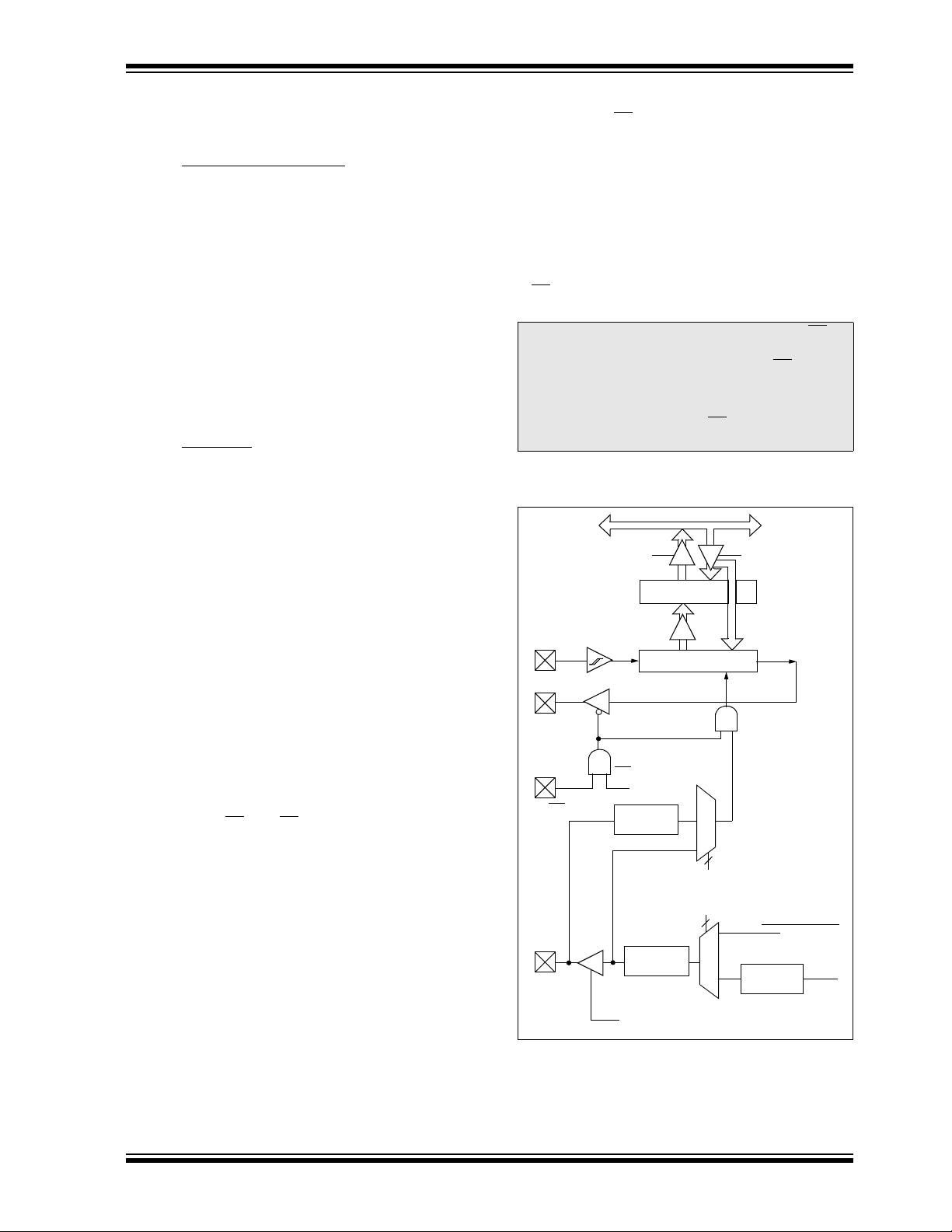
PIC16C62B/72A
Read Write
Internal
Data Bus
RC4/SDI/SDA
RC5/SDO
RA5/SS/AN4
RC3/SCK/
SSPSR reg
SSPBUF reg
SSPM3:SSPM0
bit0
Shift
Clock
SS
Control
Enable
Edge
Select
Clock Select
TMR2 output
T
CY
Prescaler
4, 16, 64
TRISC<3>
2
Edge
Select
2
4
SCL
8.0 SYNCHRONOUS SERIAL PORT
(SSP) MODULE
8.1 SSP Module Overview
The Synchronous Serial Port (SSP) module is a serial
interface useful for communicating with other peripheral or microcontroller devices. These peripheral
devices may be Serial EEPROMs, shift registers, display drivers, A/D converters, etc. The SSP module can
operate in one of two modes:
• Serial Peripheral Interface (SPI)
• Inter-Integrated Circuit (I
For more information on SSP operation (including an
I2C Overview), refer to the PIC® MCU Mid-Range Reference Manual, (DS33023). Also, refer to Application
Note AN578,
“Use of the SSP Module in the I2C Multi-
Master Environment.”
8.2 SPI Mode
This section contains register definitions and operational characteristics of the SPI module.
Additional information on SPI operation may be found
in the PIC
(DS33023).
®
MCU Mid-Range Reference Manual,
2
C)
ister, and then set bit SSPEN. This configures the SDI,
SDO, SCK and SS
pins as serial port pins. For the pins
to behave as the serial port function, they must have
their data direction bits (in the TRISC register) appropriately programmed. That is:
• SDI must have TRISC<4> set
• SDO must have TRISC<5> cleared
• SCK (master operation) must have TRISC<3>
cleared
• SCK (Slave mode) must have TRISC<3> set
•SS
must have TRISA<5> set (if used)
Note: When the SPI is in Slave Mode with SS pin
control enabled, (SSPCON<3:0> = 0100)
the SPI module will reset if the SS pin is set
DD.
to V
Note: If the SPI is used in Slave Mode with
CKE = '1', then the SS pin control must be
enabled.
FIGURE 8-1: SSP BLOCK DIAGRAM
(SPI MODE)
8.2.1 OPERATION OF SSP MODULE IN SPI
MODE
A block diagram of the SSP Module in SPI Mode is
shown in Figure 8-1.
The SPI mode allows 8-bits of data to be synchronously transmitted and received simultaneously. To
accomplish communication, three pins are used:
• Serial Data Out (SDO)RC5/SDO
• Serial Data In (SDI)RC4/SDI/SDA
• Serial Clock (SCK)RC3/SCK/SCL
Additionally, a fourth pin may be used when in a slave
mode of operation:
•Slave Select (SS
When initializing the SPI, several options need to be
specified. This is done by programming the appropriate
control bits in the SSPCON register (SSPCON<5:0>)
)RA5/SS/AN4
and SSPSTAT<7:6>. These control bits allow the following to be specified:
• Master Operation (SCK is the clock output)
• Slave Mode (SCK is the clock input)
• Clock Polarity (Idle state of SCK)
• Clock Edge (Output data on rising/falling edge of
SCK)
• Clock Rate (master operation only)
• Slave Select Mode (Slave mode only)
To enable the serial port, SSP Enable bit, SSPEN
(SSPCON<5>) must be set. To reset or reconfigure SPI
mode, clear bit SSPEN, re-initialize the SSPCON reg-
1998-2013 Microchip Technology Inc. Preliminary DS35008C-page 39
Page 40

PIC16C62B/72A
TABLE 8-1 REGISTERS ASSOCIATED WITH SPI OPERATION
Value on
Address Name Bit 7 Bit 6 Bit 5 Bit 4 Bit 3 Bit 2 Bit 1 Bit 0
0Bh,8Bh INTCON GIE PEIE
0Ch PIR1
8Ch PIE1
13h SSPBUF Synchronous Serial Port Receive Buffer/Transmit Register xxxx xxxx uuuu uuuu
14h SSPCON WCOL SSPOV SSPEN CKP SSPM3 SSPM2 SSPM1 SSPM0 0000 0000 0000 0000
94h SSPSTAT SMP CKE
85h TRISA
87h TRISC PORTC Data Direction Register 1111 1111 1111 1111
Legend: x = unknown, u = unchanged, - = unimplemented read as '0'. Shaded cells are not used by the SSP in SPI mode.
—
—
— — PORTA Data Direction Register --11 1111 --11 1111
ADIF — —SSPIFCCP1IF TMR2IF TMR1IF -0-- 0000 -0-- 0000
ADIE — —SSPIECCP1IE TMR2IE TMR1IE -0-- 0000 -0-- 0000
T0IE INTE RBIE T0IF INTF RBIF 0000 000x 0000 000u
D/A P S R/W UA BF 0000 0000 0000 0000
POR,
BOR
Value on
all other
resets
DS35008C-page 40 Preliminary 1998-2013 Microchip Technology Inc.
Page 41
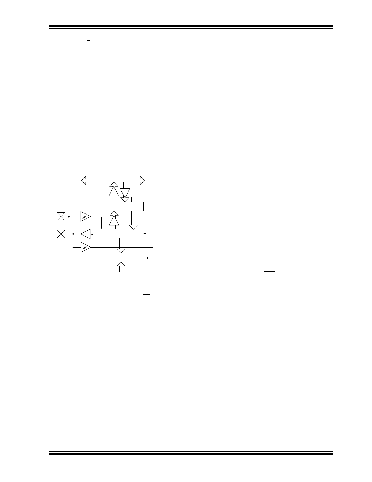
8.3 SSP I2C Operation
Read Write
SSPSR reg
Match detect
SSPADD reg
Start and
Stop bit detect
SSPBUF reg
Internal
Data Bus
Addr Match
Set, Reset
S, P bits
(SSPSTAT reg)
RC3/SCK/SCL
RC4/
shift
clock
MSb
SDI/
LSb
SDA
The SSP module in I2C mode fully implements all slave
functions, except general call support, and provides
interrupts on start and stop bits in hardware to support
firmware implementations of the master functions. The
SSP module implements the standard mode specifications, as well as 7-bit and 10-bit addressing.
Two pins are used for data transfer. These are the
RC3/SCK/SCL pin, which is the clock (SCL), and the
RC4/SDI/SDA pin, which is the data (SDA). The user
must configure these pins as inputs or outputs through
the TRISC<4:3> bits.
The SSP module functions are enabled by setting SSP
Enable bit SSPEN (SSPCON<5>).
FIGURE 8-2: SSP BLOCK DIAGRAM
2
(I
C MODE)
PIC16C62B/72A
2
The SSPCON register allows control of the I
tion. Four mode selection bits (SSPCON<3:0>) allow
one of the following I
2
C Slave mode (7-bit address)
•I
2
C modes to be selected:
•I2C Slave mode (10-bit address)
•I2C Slave mode (7-bit address), with start and
stop bit interrupts enabled for firmware master
mode support
2
C Slave mode (10-bit address), with start and
•I
stop bit interrupts enabled for firmware master
mode support
2
•I
C start and stop bit interrupts enabled for firm-
ware master mode support, slave mode idle
Selection of any I2C mode, with the SSPEN bit set,
forces the SCL and SDA pins to be operated as open
drain outputs, provided these pins are programmed to
inputs by setting the appropriate TRISC bits.
2
Additional information on SSP I
found in the PIC
®
MCU Mid-Range Reference Manual,
C operation may be
(DS33023).
8.3.1 SLAVE MODE
C opera-
The SSP module has five registers for I2C operation.
These are the:
• SSP Control Register (SSPCON)
• SSP Status Register (SSPSTAT)
• Serial Receive/Transmit Buffer (SSPBUF)
• SSP Shift Register (SSPSR) - Not accessible
• SSP Address Register (SSPADD)
In slave mode, the SCL and SDA pins must be configured as inputs (TRISC<4:3> set). The SSP module will
override the input state with the output data when
required (slave-transmitter).
When an address is matched or the data transfer after
an address match is received, the hardware automatically will generate the acknowledge (ACK
) pulse, and
load the SSPBUF register with the received value in the
SSPSR register.
There are certain conditions that will cause the SSP
module not to give this ACK
pulse. This happens if
either of the following conditions occur:
a) The buffer full bit BF (SSPSTAT<0>) was set
before the transfer was completed.
b) The overflow bit SSPOV (SSPCON<6>) was set
before the transfer was completed.
In this case, the SSPSR register value is not loaded
into the SSPBUF, but bit SSPIF (PIR1<3>) is set.
Table 8-2 shows what happens when a data transfer
byte is received, given the status of bits BF and SSPOV.
The shaded cells show the condition where user software did not properly clear the overflow condition. Flag
bit BF is cleared by reading the SSPBUF register, while
bit SSPOV is cleared through software.
The SCL clock input must have a minimum high and
low for proper operation. The high and low times of the
2
C specification, as well as the requirement of the SSP
I
module, is shown in timing parameter #100, T
parameter #101, T
LOW.
HIGH, and
1998-2013 Microchip Technology Inc. Preliminary DS35008C-page 41
Page 42

PIC16C62B/72A
8.3.1.1 ADDRESSING
Once the SSP module has been enabled, it waits for a
START condition to occur. Following the START condition, 8 bits are shifted into the SSPSR register. All
incoming bits are sampled with the rising edge of the
clock (SCL) line. The value of register SSPSR<7:1> is
compared to the value of the SSPADD register. The
address is compared on the falling edge of the eighth
clock (SCL) pulse. If the addresses match and the BF
and SSPOV bits are clear, the following events occur:
a) The SSPSR register value is loaded into the
SSPBUF register.
b) The buffer full bit, BF is set.
c) An ACK
d) SSP interrupt flag bit, SSPIF (PIR1<3>), is set
(interrupt is generated if enabled) on the falling
edge of the ninth SCL pulse.
In 10-bit address mode, two address bytes need to be
received by the slave. The five Most Significant bits
(MSbs) of the first address byte specify if this is a 10-bit
address. Bit R/W
so the slave device will receive the second address
byte. For a 10-bit address, the first byte would equal
pulse is generated.
(SSPSTAT<2>) must specify a write
‘1111 0 A9 A8 0’, where A9 and A8 are the two MSbs
of the address. The sequence of events for 10-bit
address is as follows, with steps 7- 9 for slave-transmitter:
1. Receive first (high) byte of Address (bits SSPIF,
BF, and bit UA (SSPSTAT<1>) are set).
2. Update the SSPADD register with second (low)
byte of Address (clears bit UA and releases the
SCL line).
3. Read the SSPBUF register (clears bit BF) and
clear flag bit SSPIF.
4. Receive second (low) byte of Address (bits
SSPIF, BF, and UA are set).
5. Update the SSPADD register with the first (high)
byte of Address, if match releases SCL line, this
will clear bit UA.
6. Read the SSPBUF register (clears bit BF) and
clear flag bit SSPIF.
7. Receive repeated START condition.
8. Receive first (high) byte of Address (bits SSPIF
and BF are set).
9. Read the SSPBUF register (clears bit BF) and
clear flag bit SSPIF.
TABLE 8-2 DATA TRANSFER RECEIVED BYTE ACTIONS
Status Bits as Data
Transfer is Received
BF SSPOV
00 Ye s Ye s Ye s
10 No No Yes
11 No No Yes
0 1 Ye s No Yes
Note: Shaded cells show the conditions where the user software did not properly clear the overflow condition.
SSPSR
SSPBUF
Generate ACK
Pulse
Set bit SSPIF
(SSP Interrupt occurs
if enabled)
DS35008C-page 42 Preliminary 1998-2013 Microchip Technology Inc.
Page 43
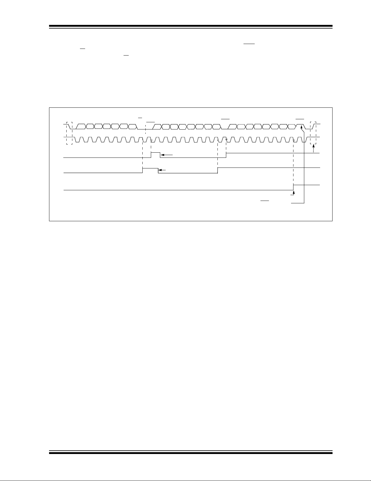
PIC16C62B/72A
P
9
8
7
6
5
D0
D1
D2
D3D4
D5
D6D7
S
A7 A6 A5 A4
A3 A2 A1SDA
SCL
1234
5
6
7
8
9
1234
56
7
89
123
4
Bus Master
terminates
transfer
Bit SSPOV is set because the SSPBUF register is still full.
Cleared in software
SSPBUF register is read
ACK
Receiving Data
Receiving Data
D0
D1
D2
D3D4
D5
D6D7
ACK
R/W=0
Receiving Address
SSPIF (PIR1<3>)
BF (SSPSTAT<0>)
SSPOV (SSPCON<6>)
ACK
ACK is not sent.
8.3.1.2 RECEPTION
When the address byte overflow condition exists, then
no acknowledge (ACK
When the R/W bit of the address byte is clear and an
address match occurs, the R/W
bit of the SSPSTAT
register is cleared. The received address is loaded into
the SSPBUF register.
dition is defined as either bit BF (SSPSTAT<0>) is set
or bit SSPOV (SSPCON<6>) is set.
An SSP interrupt is generated for each data transfer
byte. Flag bit SSPIF (PIR1<3>) must be cleared in software. The SSPSTAT register is used to determine the
status of the byte.
FIGURE 8-3: I2C WAVEFORMS FOR RECEPTION (7-BIT ADDRESS)
) pulse is given. An overflow con-
1998-2013 Microchip Technology Inc. Preliminary DS35008C-page 43
Page 44

PIC16C62B/72A
SDA
SCL
SSPIF (PIR1<3>)
BF (SSPSTAT<0>)
CKP (SSPCON<4>)
A7 A6 A5 A4 A3 A2 A1 ACK D7 D6 D5 D4 D3 D2 D1 D0
ACK
Transmitting DataR/W = 1Receiving Address
123456789 123456789
P
cleared in software
SSPBUF is written in software
From SSP interrupt
service routine
Set bit after writing to SSPBUF
S
Data in
sampled
SCL held low
while CPU
responds to SSPIF
(the SSPBUF must be written-to
before the CKP bit can be set)
8.3.1.3 TRANSMISSION
When the R/W
and an address match occurs, the R/W
bit of the incoming address byte is set
bit of the
SSPSTAT register is set. The received address is
loaded into the SSPBUF register. The ACK pulse will
be sent on the ninth bit and the CKP will be cleared by
hardware, holding SCL low. Slave devices cause the
master to wait by holding the SCL line low. The transmit
data is loaded into the SSPBUF register, which in turn
loads the SSPSR register. When bit CKP (SSPCON<4>) is set, pin RC3/SCK/SCL releases SCL.
When the SCL line goes high, the master may resume
operating the SCL line and receiving data. The master
must monitor the SCL pin prior to asserting another
clock pulse. The slave devices may be holding off the
master by stretching the clock. The eight data bits are
shifted out on the falling edge of the SCL input. This
ensures that the SDA signal is valid during the SCL
high time (Figure 8-4).
An SSP interrupt is generated for each data transfer
byte. Flag bit SSPIF must be cleared in software, and
the SSPSTAT register used to determine the status of
the byte. Flag bit SSPIF is set on the falling edge of the
ninth clock pulse.
As a slave-transmitter, the ACK
receiver is latched on the rising edge of the ninth SCL
input pulse. If the SDA line was high (not ACK
data transfer is complete. When the ACK
the slave, the slave logic is reset (resets SSPSTAT register) and the slave then monitors for another occurrence of the START bit. If the SDA line was low (ACK
the transmit data must be loaded into the SSPBUF register, which also loads the SSPSR register. Then pin
RC3/SCK/SCL should be enabled by setting bit CKP.
FIGURE 8-4: I2C WAVEFORMS FOR TRANSMISSION (7-BIT ADDRESS)
pulse from the master-
), then the
is latched by
),
DS35008C-page 44 Preliminary 1998-2013 Microchip Technology Inc.
Page 45

PIC16C62B/72A
8.3.2 MASTER OPERATION
Master operation is supported in firmware using interrupt generation on the detection of the START and
STOP conditions. The STOP (P) and START (S) bits
are cleared by a reset or when the SSP module is disabled. The STOP (P) and START (S) bits will toggle
based on the START and STOP conditions. Control of
2
C bus may be taken when the P bit is set, or the
the I
bus is idle and both the S and P bits are clear.
In master operation, the SCL and SDA lines are manipulated in software by clearing the corresponding
TRISC<4:3> bit(s). The output level is always low, irrespective of the value(s) in PORTC<4:3>. So when
transmitting data, a '1' data bit must have the
TRISC<4> bit set (input) and a '0' data bit must have
the TRISC<4> bit cleared (output). The same scenario
is true for the SCL line with the TRISC<3> bit.
The following events will cause SSP Interrupt Flag bit,
SSPIF, to be set (SSP Interrupt if enabled):
• START condition
• STOP condition
• Byte transfer completed
Master operation can be done with either the slave
mode idle (SSPM3:SSPM0 = 1011) or with the slave
active. When both master operation and slave modes
are used, the software needs to differentiate the
source(s) of the interrupt.
For more information on master operation, see
- Software Implementation of I
2
C Bus Master
AN554
.
8.3.3 MULTI-MASTER OPERATION
In multi-master operation, the interrupt generation on
the detection of the START and STOP conditions
allows the determination of when the bus is free. The
STOP (P) and START (S) bits are cleared from a reset
or when the SSP module is disabled. The STOP (P)
and START (S) bits will toggle based on the START and
STOP conditions. Control of the I
2
C bus may be taken
when bit P (SSPSTAT<4>) is set, or the bus is idle and
both the S and P bits clear. When the bus is busy,
enabling the SSP Interrupt will generate the interrupt
when the STOP condition occurs.
In multi-master operation, the SDA line must be monitored to see if the signal level is the expected output
level. This check only needs to be done when a high
level is output. If a high level is expected and a low level
is present, the device needs to release the SDA and
SCL lines (set TRISC<4:3>). There are two stages
where this arbitration can be lost, these are:
• Address Transfer
• Data Transfer
When the slave logic is enabled, the slave continues to
receive. If arbitration was lost during the address transfer stage, communication to the device may be in progress. If addressed, an ACK
pulse will be generated. If
arbitration was lost during the data transfer stage, the
device will need to re-transfer the data at a later time.
For more information on master operation, see
- Use of the SSP Module in the of I
Environment
.
2
C Multi-Master
AN578
TABLE 8-3 REGISTERS ASSOCIATED WITH I2C OPERATION
Address Name Bit 7 Bit 6 Bit 5 Bit 4 Bit 3 Bit 2 Bit 1 Bit 0
0Bh, 8Bh INTCON GIE PEIE
0Ch
8Ch
13h SSPBUF Synchronous Serial Port Receive Buffer/Transmit Register
93h SSPADD Synchronous Serial Port (I
14h SSPCON WCOL SSPOV SSPEN CKP SSPM3 SSPM2 SSPM1 SSPM0
94h SSPSTAT SMP
87h TRISC
Legend: x = unknown, u = unchanged, - = unimplemented locations read as '0'.
Note 1: Maintain these bits clear in I
PIR1
PIE1
Shaded cells are not used by SSP module in SPI mode.
—
—
PORTC Data Direction register
ADIF
ADIE
(1)
CKE
2
C mode.
T0IE INTE RBIE T0IF INTF RBIF
SSPIF
— —
— —
2
C mode) Address Register
(1)
D/A PSR/WUA BF
SSPIE
CCP1IF TMR2IF TMR1IF -0-- 0000 -0-- 0000
CCP1IE TMR2IE TMR1IE -0-- 0000 -0-- 0000
Val ue o n
POR,
BOR
0000 000x 0000 000u
xxxx xxxx uuuu uuuu
0000 0000 0000 0000
0000 0000 0000 0000
0000 0000 0000 0000
1111 1111 1111 1111
Value on
all other
resets
1998-2013 Microchip Technology Inc. Preliminary DS35008C-page 45
Page 46

PIC16C62B/72A
REGISTER 8-1: SSPSTAT: SYNC SERIAL PORT STATUS REGISTER (ADDRESS 94h)
R/W-0 R/W-0 R-0 R-0 R-0 R-0 R-0 R-0
SMP CKE D/A
bit7 bit0
bit 7: SMP: SPI data input sample phase
SPI Master Operation
1 = Input data sampled at end of data output time
0 = Input data sampled at middle of data output time
SPI Slave Mode
SMP must be cleared when SPI is used in slave mode
2
I
C Mode
This bit must be maintained clear
bit 6: CKE: SPI Clock Edge Select
SPI Mode
CKP = 0
1 = Data transmitted on rising edge of SCK
0 = Data transmitted on falling edge of SCK
CKP = 1
1 = Data transmitted on falling edge of SCK
0 = Data transmitted on rising edge of SCK
I2C Mode
This bit must be maintained clear
bit 5: D/A
bit 4: P: Stop bit (I
bit 3: S: Start bit (I
bit 2: R/W
bit 1: UA: Update Address (10-bit I
bit 0: BF: Buffer Full Status bit
: Data/Address bit (I2C mode only)
1 = Indicates that the last byte received or transmitted was data
0 = Indicates that the last byte received or transmitted was address
2
detected last, SSPEN is cleared)
1 = Indicates that a stop bit has been detected last (this bit is '0' on RESET)
0 = Stop bit was not detected last
2
detected last, SSPEN is cleared)
1 = Indicates that a start bit has been detected last (this bit is '0' on RESET)
0 = Start bit was not detected last
: Read/Write bit information (I2C mode only)
This bit holds the R/W bit information following the last address match. This bit is only valid from the
address match to the next start bit, stop bit, or ACK
1 = Read
0 = Write
1 = Indicates that the user needs to update the address in the SSPADD register
0 = Address does not need to be updated
Receive
1 = Receive complete, SSPBUF is full
0 = Receive not complete, SSPBUF is empty
Transmit
1 = Transmit in progress, SSPBUF is full
0 = Transmit complete, SSPBUF is empty
(SPI and I2C modes)
(I2C mode only)
PSR/WUA BF R = Readable bit
W = Writable bit
U = Unimplemented bit, read
as ‘0’
- n =Value at POR reset
C mode only. This bit is cleared when the SSP module is disabled, or when the Start bit is
C mode only. This bit is cleared when the SSP module is disabled, or when the Stop bit is
bit.
2
C mode only)
DS35008C-page 46 Preliminary 1998-2013 Microchip Technology Inc.
Page 47

PIC16C62B/72A
REGISTER 8-2: SSPCON: SYNC SERIAL PORT CONTROL REGISTER (ADDRESS 14h)
R/W-0 R/W-0 R/W-0 R/W-0 R/W-0 R/W-0 R/W-0 R/W-0
WCOL SSPOV SSPEN CKP SSPM3 SSPM2 SSPM1 SSPM0 R = Readable bit
bit7 bit0
bit 7: WCOL: Write Collision Detect bit
1 = The SSPBUF register is written while it is still transmitting the previous word
(must be cleared in software)
0 = No collision
bit 6: SSPOV: Receive Overflow Indicator bit
In SPI mode
1 = A new byte is received while the SSPBUF register is still holding the previous data. In case of overflow,
the data in SSPSR is lost. Overflow can only occur in slave mode. The user must read the SSPBUF, even
if only transmitting data, to avoid setting overflow. In master operation, the overflow bit is not set since
each new reception (and transmission) is initiated by writing to the SSPBUF register.
0 = No overflow
2
C mode
In I
1 = A byte is received while the SSPBUF register is still holding the previous byte. SSPOV is a "don’t care"
in transmit mode. SSPOV must be cleared in software in either mode.
0 = No overflow
bit 5: SSPEN: Synchronous Serial Port Enable bit
In SPI mode
1 = Enables serial port and configures SCK, SDO, and SDI as serial port pins
0 = Disables serial port and configures these pins as I/O port pins
In I2C mode
1 = Enables the serial port and configures the SDA and SCL pins as serial port pins
0 = Disables serial port and configures these pins as I/O port pins
In both modes, when enabled, these pins must be properly configured as input or output.
bit 4: CKP: Clock Polarity Select bit
In SPI mode
1 = Idle state for clock is a high level
0 = Idle state for clock is a low level
In I2C mode
SCK release control
1 = Enable clock
0 = Holds clock low (clock stretch)
bit 3-0: SSPM3:SSPM0: Synchronous Serial Port Mode Select bits
0000 = SPI master operation, clock = F
0001 = SPI master operation, clock = F
0010 = SPI master operation, clock = F
OSC/4
OSC/16
OSC/64
0011 = SPI master operation, clock = TMR2 output/2
0100 = SPI slave mode, clock = SCK pin. SS
0101 = SPI slave mode, clock = SCK pin. SS
0110 = I
0111 = I
1011 = I
1110 = I
1111 = I
2
C slave mode, 7-bit address
2
C slave mode, 10-bit address
2
C firmware controlled master operation (slave idle)
2
C slave mode, 7-bit address with start and stop bit interrupts enabled
2
C slave mode, 10-bit address with start and stop bit interrupts enabled
pin control enabled.
pin control disabled. SS can be used as I/O pin
W = Writable bit
U = Unimplemented bit, read
as ‘0’
- n =Value at POR reset
1998-2013 Microchip Technology Inc. Preliminary DS35008C-page 47
Page 48

PIC16C62B/72A
NOTES:
DS35008C-page 48 Preliminary 1998-2013 Microchip Technology Inc.
Page 49

PIC16C62B/72A
9.0 ANALOG-TO-DIGITAL
CONVERTER (A/D) MODULE
Note: This section applies to the PIC16C72A
only.
The analog-to-digital (A/D) converter module has five
input channels.
The A/D allows conversion of an analog input signal to
a corresponding 8-bit digital number (refer to Application Note AN546 for use of A/D Converter). The output
of the sample and hold is the input into the converter,
which generates the result via successive approximation. The analog reference voltage is software selectable to either the device’s positive supply voltage (V
or the voltage level on the RA3/AN3/V
The A/D converter has the feature of being able to
operate while the device is in SLEEP mode. To operate
in sleep, the A/D conversion clock must be derived from
the A/D’s internal RC oscillator.
REF pin.
DD)
Additional information on the A/D module is available in
the PIC
(DS33023).
The A/D module has three registers. These registers
are:
A device reset forces all registers to their reset state.
This forces the A/D module to be turned off, and any
conversion is aborted.
The ADCON0 register, shown in Figure 9-1, controls
the operation of the A/D module. The ADCON1 register, shown in Figure 9-2, configures the functions of the
port pins. The port pins can be configured as analog
inputs (RA3 can also be a voltage reference) or as digital I/O.
®
MCU Mid-Range Reference Manual,
• A/D Result Register (ADRES)
• A/D Control Register 0 (ADCON0)
• A/D Control Register 1 (ADCON1)
REGISTER 9-1:ADCON0 REGISTER (ADDRESS 1Fh)
R/W-0 R/W-0 R/W-0 R/W-0 R/W-0 R/W-0 U-0 R/W-0
ADCS1 ADCS0 CHS2 CHS1 CHS0 GO/DONE — ADON R =Readable bit
bit7 bit0
bit 7-6: ADCS1:ADCS0: A/D Conversion Clock Select bits
OSC/2
00 = F
01 = F
OSC/8
OSC/32
10 = F
RC (clock derived from an internal RC oscillator)
11 = F
bit 5-3: CHS2:CHS0: Analog Channel Select bits
000 = channel 0, (RA0/AN0)
001 = channel 1, (RA1/AN1)
010 = channel 2, (RA2/AN2)
011 = channel 3, (RA3/AN3)
100 = channel 4, (RA5/AN4)
bit 2: GO/DONE
If ADON = 1
1 = A/D conversion in progress (setting this bit starts the A/D conversion)
0 = A/D conversion not in progress (This bit is automatically cleared by hardware when the A/D
conversion is complete)
bit 1: Unimplemented: Read as '0'
bit 0: ADON: A/D On bit
1 = A/D converter module is operating
0 = A/D converter module is shutoff and consumes no operating current
: A/D Conversion Status bit
W = Writable bit
U = Unimplemented bit,
read as ‘0’
- n = Value at POR reset
1998-2013 Microchip Technology Inc. Preliminary DS35008C-page 49
Page 50

PIC16C62B/72A
A = Analog input
D = Digital I/O
PCFG2:PCFG0 RA0 RA1 RA2 RA5 RA3 V
REF
000 AAAAA VDD
001 AAAAVREF RA3
010 AAAAA VDD
011 AAAAVREF RA3
100 AADDA V
DD
101 AADDVREF RA3
11x DDDDD V
DD
REGISTER 9-2:ADCON1 REGISTER (ADDRESS 9Fh)
U-0 U-0 U-0 U-0 U-0 R/W-0 R/W-0 R/W-0
— — — — — PCFG2 PCFG1 PCFG0 R = Readable bit
bit7 bit0
bit 7-3: Unimplemented: Read as '0'
bit 2-0: PCFG2:PCFG0: A/D Port Configuration Control bits
W = Writable bit
U = Unimplemented bit,
- n = Value at POR
read as ‘0’
reset
DS35008C-page 50 Preliminary 1998-2013 Microchip Technology Inc.
Page 51

PIC16C62B/72A
(Input voltage)
V
IN
VREF
(Reference
voltage)
V
DD
PCFG2:PCFG0
CHS2:CHS0
000 or
010 or
100 or
001 or
011 or
101
RA5/AN4
RA3/AN3/V
REF
RA2/AN2
RA1/AN1
RA0/AN0
100
011
010
001
000
A/D
Converter
11x
When the A/D conversion is complete, the result is
loaded into the ADRES register, the GO/DONE
bit,
ADCON0<2>, is cleared, and the A/D interrupt flag bit,
ADIF, is set. The block diagram of the A/D module is
shown in Figure 9-1.
The value that is in the ADRES register is not modified
for a Power-on Reset. The ADRES register will contain
unknown data after a Power-on Reset.
After the A/D module has been configured as desired,
the selected channel must be acquired before the conversion is started. The analog input channels must
have their corresponding TRIS bits selected as an
input. To determine acquisition time, see Section 9.1.
After this acquisition time has elapsed, the A/D conversion can be started. The following steps should be followed for doing an A/D conversion:
1. Configure the A/D module:
• Configure analog pins / voltage reference /
and digital I/O (ADCON1)
• Select A/D input channel (ADCON0)
• Select A/D conversion clock (ADCON0)
• Turn on A/D module (ADCON0)
2. Configure A/D interrupt (if desired):
• Clear ADIF bit
• Set ADIE bit
• Set GIE bit
3. Wait the required acquisition time.
4. Start conversion:
• Set GO/DONE
bit (ADCON0)
5. Wait for A/D conversion to complete, by either:
• Polling for the GO/DONE bit to be cleared
OR
• Waiting for the A/D interrupt
6. Read A/D Result register (ADRES), clear bit
ADIF if required.
7. For next conversion, go to step 1 or step 2 as
required. The A/D conversion time per bit is
defined as T
AD. A minimum wait of 2TAD is
required before next acquisition starts.
FIGURE 9-1: A/D BLOCK DIAGRAM
1998-2013 Microchip Technology Inc. Preliminary DS35008C-page 51
Page 52

PIC16C62B/72A
CPIN
VA
Rs
ANx
5 pF
V
DD
VT = 0.6V
VT = 0.6V
I leakage
R
IC 1k
Sampling
Switch
SS
R
SS
CHOLD
= DAC capacitance
V
SS
6V
R
SS
5V
4V
3V
2V
567891011
(k)
VDD
= 51.2 pF
± 500 nA
Legend CPIN
VT
I leakage
R
IC
SS
C
HOLD
= input capacitance
= threshold voltage
= leakage current at the pin due to
= interconnect resistance
= sampling switch
= sample/hold capacitance (from DAC)
various junctions
9.1 A/D Acquisition Requirements
For the A/D converter to meet its specified accuracy,
the charge holding capacitor (C
HOLD) must be allowed
to fully charge to the input channel voltage level. The
analog input model is shown in Figure 9-2. The source
impedance (R
S) and the internal sampling switch (RSS)
impedance directly affect the time required to charge
the capacitor C
impedance varies over the device voltage (V
HOLD. The sampling switch (RSS)
DD). The
source impedance affects the offset voltage at the analog input (due to pin leakage current). The maximum
recommended impedance for analog sources is 10
k. After the analog input channel is selected
(changed), this acquisition must pass before the conversion can be started.
FIGURE 9-2: ANALOG INPUT MODEL
To calculate the minimum acquisition time, T
ACQ, see
Equation 9-1. This equation calculates the acquisition
time to within 1/2 LSb error (512 steps for the A/D). The
1/2 LSb error is the maximum error allowed for the A/D
to meet its specified accuracy.
Note: When the conversion is started, the hold-
ing capacitor is disconnected from the
input pin.
In general;
Assuming R
S = 10k
Vdd = 3.0V (R
SS = 10k
Te m p . = 5 0 C (122F)
ACQ 13.0 Sec
T
By increasing V
DD and reducing RS and Temp., TACQ
can be substantially reduced.
EQUATION 9-1: ACQUISITION TIME
TACQ ==Amplifier Settling Time +
Hold Capacitor Charging Time +
Temperature Coefficient
TAMP + TC + TCOFF
TAMP = 5S
C = - (51.2pF)(1k + RSS + RS) In(1/511)
T
T
COFF = (Temp -25C)(0.05S/C)
DS35008C-page 52 Preliminary 1998-2013 Microchip Technology Inc.
Page 53

PIC16C62B/72A
9.2 Selecting the A/D Conversion Clock
The A/D conversion time per bit is defined as TAD. The
A/D conversion requires 9.5T
The source of the A/D conversion clock is software
selectable. The four possible options for TAD are:
OSC
•2T
•8TOSC
•32TOSC
• Internal RC oscillator
For correct A/D conversions, the A/D conversion clock
AD) must be selected to ensure a minimum TAD time
(T
of 1.6 s.
The A/D module can operate during sleep mode, but
the RC oscillator must be selected as the A/D clock
source prior to the SLEEP instruction.
Table 9-1 shows the resultant T
the device operating frequencies and the A/D clock
source selected.
AD per 8-bit conversion.
AD times derived from
9.3 Configuring Analog Port Pins
The ADCON1 and TRISA registers control the operation of the A/D port pins. The port pins that are desired
as analog inputs must have their corresponding TRIS
bits set (input). If the TRIS bit is cleared (output), the
digital output level (V
The A/D operation is independent of the state of the
CHS2:CHS0 bits and the TRIS bits.
Note 1: When reading the port register, all pins
configured as analog input channels will
read as cleared (a low level). Pins configured as digital inputs, will convert an analog input. Analog levels on a digitally
configured input will not affect the conversion accuracy.
Note 2: Analog levels on any pin that is defined as
a digital input (including the AN4:AN0
pins) may cause the input buffer to consume current that is out of the devices
OH or VOL) will be converted.
specification.
TABLE 9-1 TAD vs. DEVICE OPERATING FREQUENCIES
AD Clock Source (TAD) Device Frequency
Operation ADCS1:ADCS0 20 MHz 5 MHz 1.25 MHz 333.33 kHz
OSC 00
2T
8TOSC 01
100 ns
400 ns
(2)
(2)
32TOSC 10 1.6 s6.4 s
RC
(5)
11
2 - 6 s
(1,4)
2 - 6 s
Legend: Shaded cells are outside of recommended range.
Note 1: The RC source has a typical T
2: These values violate the minimum required T
AD time of 4 s.
AD time.
3: For faster conversion times, the selection of another clock source is recommended.
4: When device frequency is greater than 1 MHz, the RC A/D conversion clock source is recommended for
sleep operation only.
5: For extended voltage devices (LC), please refer to Electrical Specifications section.
400 ns
(2)
1.6 s6 s
1.6 s6.4 s
25.6 s
(1,4)
2 - 6 s
(3)
(1,4)
24 s
96 s
2 - 6 s
(3)
(3)
(1)
1998-2013 Microchip Technology Inc. Preliminary DS35008C-page 53
Page 54

PIC16C62B/72A
9.4 A/D Conversions
GO/DONE
bit will be set, starting the A/D conversion,
and the Timer1 counter will be reset to zero. Timer1 is
Note: The GO/DONE bit should NOT be set in
the same instruction that turns on the A/D.
reset to automatically repeat the A/D acquisition period
with minimal software overhead. The appropriate analog input channel must be selected and the minimum
9.5 Use of the CCP Trigger
An A/D conversion can be started by the “special event
trigger” of the CCP1 module. This requires that the
CCP1M3:CCP1M0 bits (CCP1CON<3:0>) be programmed as 1011 and that the A/D module be enabled
acquisition time must pass before the “special event
trigger” sets the GO/DONE
bit (starts a conversion).
If the A/D module is not enabled (ADON is cleared),
then the “special event trigger” will be ignored by the
A/D module, but will still reset the Timer1 counter.
(ADON bit is set). When the trigger occurs, the
TABLE 9-2 SUMMARY OF A/D REGISTERS
Address Name Bit 7 Bit 6 Bit 5 Bit 4 Bit 3 Bit 2 Bit 1 Bit 0
0Bh,8Bh
0Ch
8Ch
1Eh
1Fh
9Fh
05h PORTA
85h TRISA
Legend: x = unknown, u = unchanged, - = unimplemented read as '0'. Shaded cells are not used for A/D conversion.
INTCON GIE PEIE
PIR1
PIE1
ADRES A/D Result Register xxxx xxxx uuuu uuuu
ADCON0 ADCS1 ADCS0 CHS2 CHS1 CHS0 GO/DONE
ADCON1
ADIF
—
ADIE
—
— — — — — PCFG2 PCFG1 PCFG0 ---- -000 ---- -000
— — RA5 RA4 RA3 RA2 RA1 RA0
— — PORTA Data Direction Register
T0IE INTE RBIE T0IF INTF RBIF 0000 000x 0000 000u
— — SSPIF CCP1IF TMR2IF TMR1IF -0-- 0000 -0-- 0000
— — SSPIE CCP1IE TMR2IE TMR1IE -0-- 0000 -0-- 0000
—ADON0000 00-0 0000 00-0
Value on
POR,
BOR
--0x 0000 --0u 0000
--11 1111 --11 1111
Value on all
other Resets
DS35008C-page 54 Preliminary 1998-2013 Microchip Technology Inc.
Page 55

PIC16C62B/72A
10.0 SPECIAL FEATURES OF THE
CPU
The PIC16C62B/72A devices have a host of features
intended to maximize system reliability, minimize cost
through elimination of external components, provide
power saving operating modes and offer code protection. These are:
• Oscillator Mode Selection
• Reset
- Power-on Reset (POR)
- Power-up Timer (PWRT)
- Oscillator Start-up Timer (OST)
- Brown-out Reset (BOR)
• Interrupts
• Watchdog Timer (WDT)
• SLEEP
• Code protection
• ID locations
• In-circuit serial programming™ (ICSP)
These devices have a Watchdog Timer, which can be
shut off only through configuration bits. It runs off its
own RC oscillator for added reliability. There are two
timers that offer necessary delays on power-up. One is
the Oscillator Start-up Timer (OST), intended to keep
the chip in reset until the crystal oscillator is stable. The
other is the Power-up Timer (PWRT), which provides a
fixed delay on power-up only and is designed to keep
the part in reset while the power supply stabilizes. With
these two timers on-chip, most applications need no
external reset circuitry.
SLEEP mode is designed to offer a very low current
power-down mode. The user can wake-up from SLEEP
through external reset, Watchdog Timer Wake-up, or
through an interrupt. Several oscillator options are also
made available to allow the part to fit the application.
The RC oscillator option saves system cost while the
LP crystal option saves power. A set of configuration
bits are used to select various options.
Additional information on special features is available in
the PIC
®
MCU Mid-Range Reference Manual,
(DS33023).
10.1 Configuration Bits
The configuration bits can be programmed (read as '0')
or left unprogrammed (read as '1') to select various
device configurations. These bits are mapped in program memory location 2007h.
The user will note that address 2007h is beyond the
user program memory space. In fact, it belongs to the
special test/configuration memory space (2000h 3FFFh), which can be accessed only during programming.
FIGURE 10-1: CONFIGURATION WORD
CP1 CP0 CP1 CP0 CP1 CP0 — BODEN CP1 CP0 PWRTE WDTE FOSC1 FOSC0
bit13 bit0
bit 13-8 CP1:CP0: Code Protection bits
5-4: 11 = Code protection off
bit 7: Unimplemented: Read as '1'
bit 6: BODEN: Brown-out Reset Enable bit
bit 3: PWRTE
bit 2: WDTE: Watchdog Timer Enable bit
bit 1-0: FOSC1:FOSC0: Oscillator Selection bits
Note 1: Enabling Brown-out Reset automatically enables Power-up Timer (PWRT), regardless of the value of bit PWRTE
10 = Upper half of program memory code protected
01 = Upper 3/4th of program memory code protected
00 = All memory is code protected
1 = BOR enabled
0 = BOR disabled
: Power-up Timer Enable bit
1 = PWRT disabled
0 = PWRT enabled
1 = WDT enabled
0 = WDT disabled
11 = RC oscillator
10 = HS oscillator
01 = XT oscillator
00 = LP oscillator
All of the CP1:CP0 pairs must be given the same value to enable the code protection scheme listed.
(2)
(1)
(1)
Register: CONFIG
Address: 2007h
.
1998-2013 Microchip Technology Inc. Preliminary DS35008C-page 55
Page 56

PIC16C62B/72A
Note1: See Table 10-1 and Table 10-2 for recom-
mended values of C1 and C2.
2: A series resistor (RS) may be required for
AT strip cut crystals.
3: RF varies with the crystal chosen.
C1
(1)
C2
(1)
XTAL
OSC2
OSC1
RF
(3)
SLEEP
To
logic
PIC16CXXX
RS
(2)
internal
OSC1
OSC2
Open
Clock from
ext. system
PIC16CXXX
10.2 Oscillator Configurations
10.2.1 OSCILLATOR TYPES
The PIC16CXXX can be operated in four different oscillator modes. The user can program two configuration
bits (FOSC1 and FOSC0) to select one of these four
modes:
• LP Low Power Crystal
• XT Crystal/Resonator
• HS High Speed Crystal/Resonator
• RC Resistor/Capacitor
10.2.2 CRYSTAL OSCILLATOR/CERAMIC
RESONATORS
In XT, LP or HS modes, a crystal or ceramic resonator
is connected to the OSC1/CLKIN and OSC2/CLKOUT
pins to establish oscillation (Figure 10-2). The
PIC16CXXX oscillator design requires the use of a parallel cut crystal. Use of a series cut crystal may give a
frequency out of the crystal manufacturers specifications. When in XT, LP or HS modes, the device can use
an external clock source to drive the OSC1/CLKIN pin
(Figure 10-3).
FIGURE 10-2: CRYSTAL/CERAMIC
RESONATOR OPERATION
(HS, XT OR LP
OSC CONFIGURATION)
FIGURE 10-3: EXTERNAL CLOCK INPUT
OPERATION (HS, XT OR LP
OSC CONFIGURATION)
TABLE 10-1 CERAMIC RESONATORS
Ranges Tested:
Mode Freq OSC1 OSC2
XT 455 kHz
2.0 MHz
4.0 MHz
HS 8.0 MHz
16.0 MHz
These values are for design guidance only. See
notes at bottom of page.
68 - 100 pF
15 - 68 pF
15 - 68 pF
10 - 68 pF
10 - 22 pF
68 - 100 pF
15 - 68 pF
15 - 68 pF
10 - 68 pF
10 - 22 pF
Resonators Used:
455 kHz Panasonic EFO-A455K04B 0.3%
2.0 MHz Murata Erie CSA2.00MG 0.5%
4.0 MHz Murata Erie CSA4.00MG 0.5%
8.0 MHz Murata Erie CSA8.00MT 0.5%
16.0 MHz Murata Erie CSA16.00MX 0.5%
Resonators did not have built-in capacitors.
TABLE 10-2 CAPACITOR SELECTION FOR
CRYSTAL OSCILLATOR
Osc Type
LP 32 kHz 33 pF 33 pF
XT 200 kHz 47-68 pF 47-68 pF
HS 4 MHz 15 pF 15 pF
These values are for design guidance only. See
notes at bottom of page.
32 kHz Epson C-001R32.768K-A ± 20 PPM
200 kHz STD XTL 200.000KHz ± 20 PPM
1 MHz ECS ECS-10-13-1 ± 50 PPM
4 MHz ECS ECS-40-20-1 ± 50 PPM
8 MHz EPSON CA-301 8.000M-C ± 30 PPM
20 MHz EPSON CA-301 20.000M-C ± 30 PPM
Note 1: Higher capacitance increases the stability of the
2: Since each resonator/crystal has its own charac-
3: Rs may be required in HS mode, as well as XT
4: Oscillator performance should be verified when
Crystal
Freq
200 kHz 15 pF 15 pF
1 MHz 15 pF 15 pF
4 MHz 15 pF 15 pF
8 MHz 15-33 pF 15-33 pF
20 MHz 15-33 pF 15-33 pF
oscillator, but also increases the start-up time.
teristics, the user should consult the resonator/crystal manufacturer for appropriate values of
external components.
mode, to avoid overdriving crystals with low drive
level specification.
migrating between devices (including
PIC16C62A to PIC16C62B and PIC16C72 to
PIC16C72A)
Cap. Range C1Cap. Range
C2
Crystals Used
DS35008C-page 56 Preliminary 1998-2013 Microchip Technology Inc.
Page 57

PIC16C62B/72A
OSC2/CLKOUT
Cext
Rext
PIC16CXX
OSC1
Fosc/4
Internal
clock
VDD
VSS
Recommended values: 3 k Rext 100 k
Cext > 20pF
10.2.3 RC OSCILLATOR
For timing insensitive applications, the “RC” device
option offers additional cost savings. The RC oscillator
frequency is a function of the supply voltage, the resis-
EXT) and capacitor (CEXT) values, and the operat-
tor (R
ing temperature. In addition to this, the oscillator
frequency will vary from unit to unit due to normal process parameter variation. Furthermore, the difference
in lead frame capacitance between package types will
also affect the oscillation frequency, especially for low
EXT values. The user also needs to take into account
C
variation due to tolerance of external R and C components used. Figure 10-4 shows how the R/C combination is connected to the PIC16CXXX.
FIGURE 10-4: RC OSCILLATOR MODE
10.3 Reset
The PIC16CXXX differentiates between various kinds
of reset:
• Power-on Reset (POR)
•MCLR
•MCLR reset during SLEEP
• WDT Reset (during normal operation)
• WDT Wake-up (during SLEEP)
• Brown-out Reset (BOR)
Some registers are not affected in any reset condition;
their status is unknown on POR and unchanged by any
other reset. Most other registers are reset to a “reset
state” on Power-on Reset (POR), on the MCLR
WDT Reset, on MCLR
Brown-out Reset (BOR). They are not affected by a
WDT Wake-up from SLEEP, which is viewed as the
resumption of normal operation. The TO
are set or cleared depending on the reset situation, as
indicated in Table 10-4. These bits are used in software
to determine the nature of the reset. See Table 10-6 for
a full description of reset states of all registers.
A simplified block diagram of the on-chip reset circuit is
shown in Figure 10-5.
The PIC devices have a MCLR
reset path. The filter will ignore small pulses. However,
a valid MCLR
width (TmcL, Specification #30).
No internal reset source (WDT, BOR, POR) willdrive
the MCLR
reset during normal operation
and
reset during SLEEP, and on
and PD bits
noise filter in the MCLR
pulse must meet the minimum pulse
pin low.
1998-2013 Microchip Technology Inc. Preliminary DS35008C-page 57
Page 58
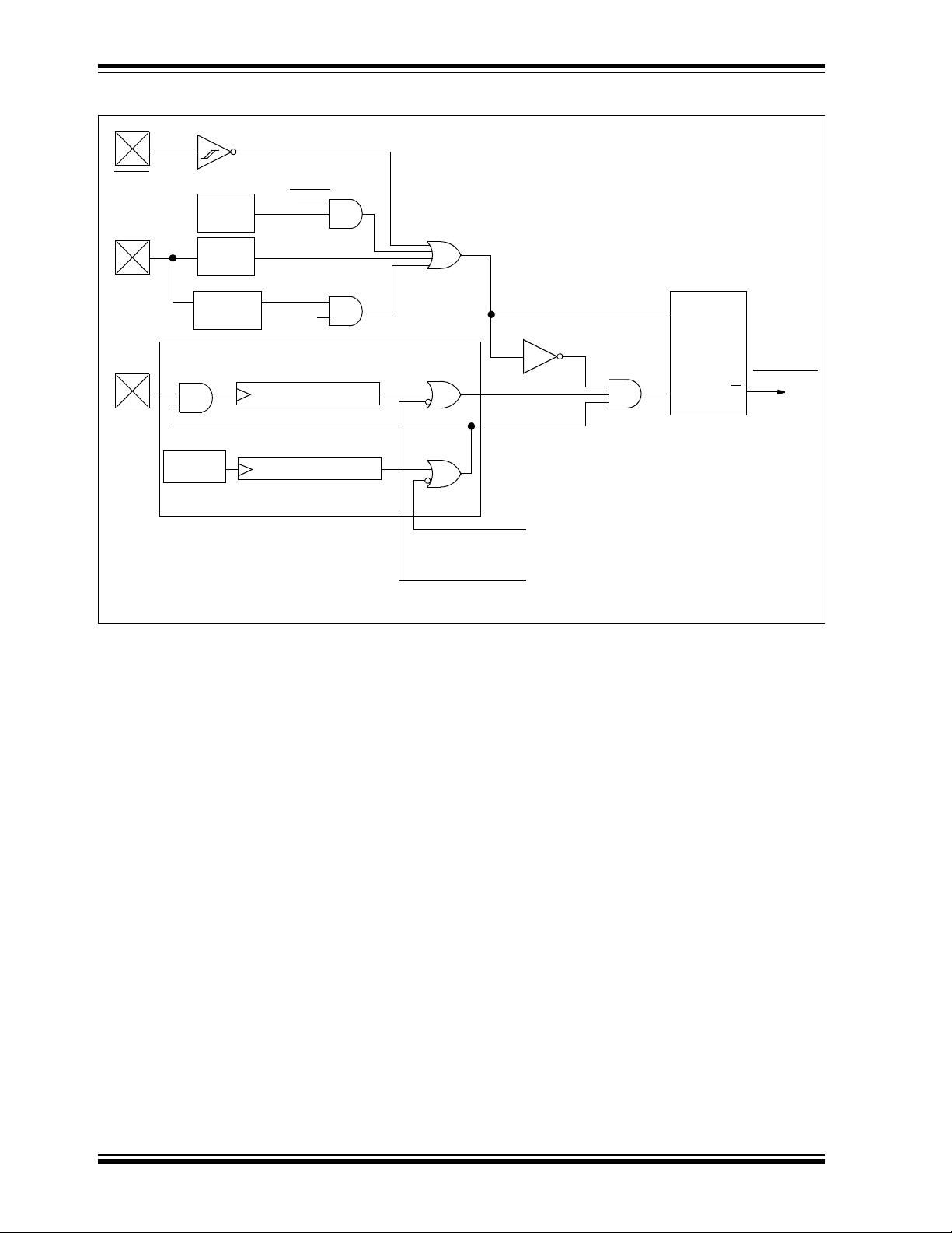
PIC16C62B/72A
S
R
Q
External
Reset
MCLR
VDD
OSC1
WDT
Module
V
DD rise
detect
OST/PWRT
On-chip
RC OSC
WDT
Time-out
Power-on Reset
OST
10-bit Ripple counter
PWRT
Chip_Reset
10-bit Ripple counter
Reset
Enable OST
Enable PWRT
SLEEP
Note 1: This is a separate oscillator from the RC oscillator of the CLKIN pin.
Brown-out
Reset
BODEN
(1)
FIGURE 10-5: SIMPLIFIED BLOCK DIAGRAM OF ON-CHIP RESET CIRCUIT
DS35008C-page 58 Preliminary 1998-2013 Microchip Technology Inc.
Page 59
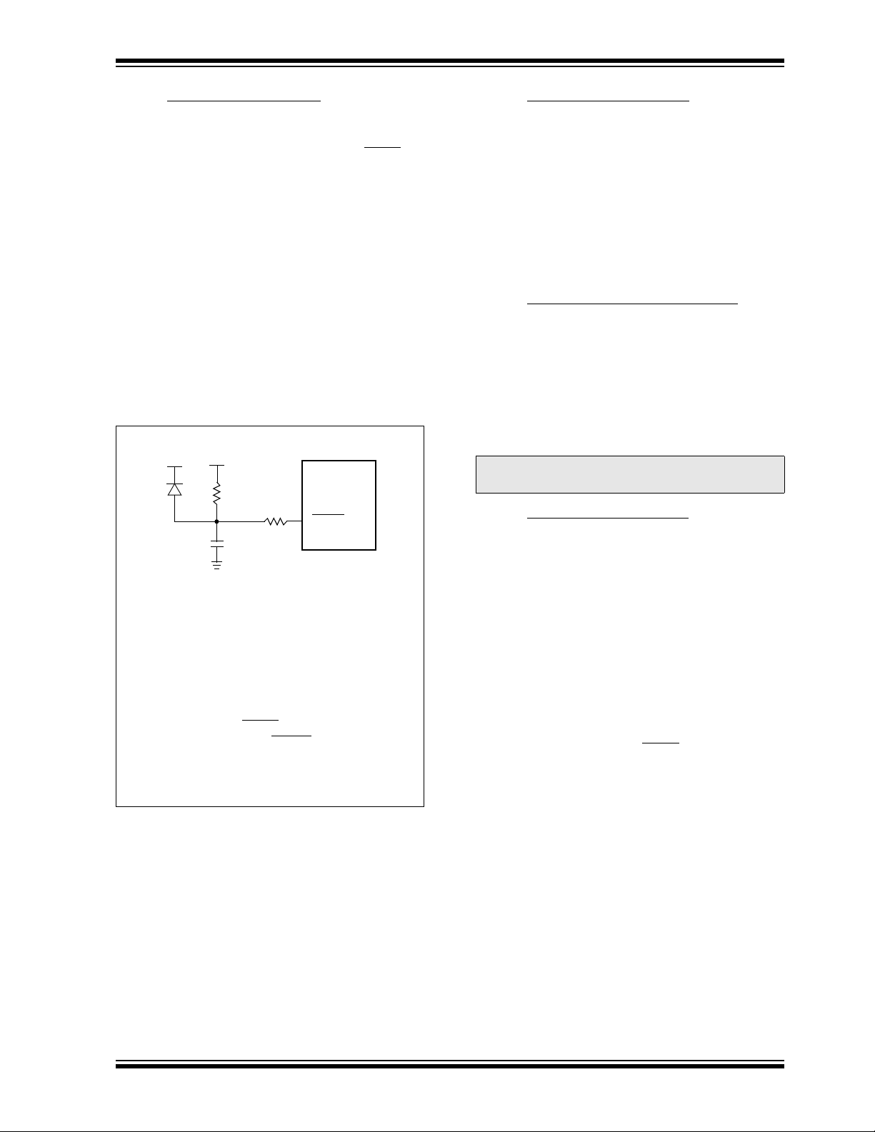
PIC16C62B/72A
Note 1: External Power-on Reset circuit is required
only if V
DD power-up slope is too slow. The
diode D helps discharge the capacitor
quickly when V
DD powers down.
2: R < 40 k is recommended to make sure
that voltage drop across R does not violate
the device’s electrical specification.
3: R1 = 100 to 1 k will limit any current
flowing into MCLR
from external capacitor
C in the event of MCLR/
VPP pin breakdown due to Electrostatic Discharge
(ESD) or Electrical Overstress (EOS).
C
R1
R
D
V
DD
MCLR
PIC16CXX
10.4 Power-On Reset (POR)
A Power-on Reset pulse is generated on-chip when
DD rise is detected (in the range of 1.5V - 2.1V). To
V
take advantage of the POR, just tie the MCLR
directly (or through a resistor) to V
DD. This will elimi-
pin
nate external RC components usually needed to create
a Power-on Reset. A maximum rise time for VDD is
specified (SV
DD, parameter D004). For a slow rise
time, see Figure 10-6.
When the device starts normal operation (exits the
reset condition), device operating parameters (voltage,
frequency, temperature,...) must be met to ensure operation. If these conditions are not met, the device must
be held in reset until the operating conditions are met.
Brown-out Reset may be used to meet the start-up conditions.
FIGURE 10-6: EXTERNAL POWER-ON
RESET CIRCUIT (FOR SLOW
V
DD POWER-UP)
10.5 Power-up Timer (PWRT)
The Power-up Timer provides a fixed nominal time-out
PWRT, parameter #33) from the POR. The Power-up
(T
Timer operates on an internal RC oscillator. The chip is
kept in reset as long as the PWRT is active. The
PWRT’s time delay allows V
DD to rise to an acceptable
level. A configuration bit is provided to enable/disable
the PWRT.
The power-up time delay will vary from chip-to-chip due
DD, temperature and process variation. See DC
to V
parameters for details.
10.6 Oscillator Start-up Timer (OST)
The Oscillator Start-up Timer (OST) provides a delay of
1024 oscillator cycles (from OSC1 input) after the
PWRT delay is over (T
ensures that the crystal oscillator or resonator has
started and stabilized.
The OST time-out is invoked only for XT, LP and HS
modes and only on Power-on Reset or wake-up from
SLEEP.
Note: The OST delay may not occur when the
device wakes from SLEEP.
OST, parameter #32). This
1998-2013 Microchip Technology Inc. Preliminary DS35008C-page 59
10.7 Brown-Out Reset (BOR)
The configuration bit, BODEN, can enable or disable
the Brown-Out Reset circuit. If V
(parameter #35, about 100S), the brown-out situation
will reset the device. If VDD falls below VBOR for less
BOR, a reset may not occur.
than T
Once the brown-out occurs, the device will remain in
brown-out reset until V
DD rises above VBOR. The
power-up timer then keeps the device in reset for
TPWRT (parameter #33, about 72mS). If VDD should fall
below V
cess will restart when V
BOR during TPWRT, the brown-out reset pro-
DD rises above VBOR with the
power-up timer reset. The power-up timer is always
enabled when the brown-out reset circuit is enabled,
regardless of the state of the PWRT
PP falls below Vbor
configuration bit.
Page 60

PIC16C62B/72A
10.8 Time-out Sequence
When a POR reset occurs, the PWRT delay starts (if
enabled). When PWRT ends, the OST counts 1024
oscillator cycles (LP, XT, HS modes only). When OST
completes, the device comes out of reset. The total
time-out will vary based on oscillator configuration and
the status of the PWRT. For example, in RC mode with
the PWRT disabled, there will be no time-out at all.
If MCLR
expire. Bringing MCLR
diately. This is useful for testing purposes or to synchronize more than one PIC16CXXX device operating in
parallel.
is kept low long enough, the time-outs will
high will begin execution imme-
Table 10-5 shows the reset conditions for the STATUS,
PCON and PC registers, while Table 10-6 shows the
reset conditions for all the registers.
10.9 Power Control/Status Register
The BOR bit is unknown on Power-on Reset. If the
Brown-out Reset circuit is used, the BOR
set by the user and checked on subsequent resets to
see if it was cleared, indicating a Brown-out has
occurred.
OR (Power-on Reset Status bit) is cleared on a
P
Power-on Reset and unaffected otherwise. The user
Status Register
IRP RP1 RP0 TO PD Z DC C
PCON Register
POR BOR
TABLE 10-3 TIME-OUT IN VARIOUS SITUATIONS
Oscillator Configuration
PWRTE
XT, HS, LP 72 ms + 1024T
RC 72 ms — 72 ms —
Power-up
= 0 PWRTE = 1
OSC 1024TOSC 72 ms + 1024TOSC 1024TOSC
(PCON)
Brown-out
bit must be
Wake-up from
SLEEP
TABLE 10-4 STATUS BITS AND THEIR SIGNIFICANCE
POR BOR TO PD
0x11Power-on Reset
0x0xIllegal, TO
0xx0Illegal, PD is set on POR
1011Brown-out Reset
1101WDT Reset
1100WDT Wake-up
11uuMCLR
1110MCLR
is set on POR
Reset during normal operation
Reset during SLEEP or interrupt wake-up from SLEEP
TABLE 10-5 RESET CONDITION FOR SPECIAL REGISTERS
Condition
Power-on Reset 000h 0001 1xxx ---- --0x
MCLR
Reset during normal operation 000h 000u uuuu ---- --uu
MCLR Reset during SLEEP 000h 0001 0uuu ---- --uu
WDT Reset 000h 0000 1uuu ---- --uu
WDT Wake-up PC + 1 uuu0 0uuu ---- --uu
Brown-out Reset 000h 0001 1uuu ---- --u0
Interrupt wake-up from SLEEP PC + 1
Program
Counter
(1)
STATUS
Register
uuu1 0uuu ---- --uu
PCON
Register
Legend: u = unchanged, x = unknown, - = unimplemented bit read as '0'.
Note 1: When the wake-up is due to an interrupt and the GIE bit is set, the PC is loaded with the interrupt vector (0004h).
DS35008C-page 60 Preliminary 1998-2013 Microchip Technology Inc.
Page 61

PIC16C62B/72A
TABLE 10-6 INITIALIZATION CONDITIONS FOR ALL REGISTERS
Register Applicable
Devices
W62B72Axxxx xxxx uuuu uuuu uuuu uuuu
INDF 62B 72A N/A N/A N/A
TMR0 62B 72A xxxx xxxx uuuu uuuu uuuu uuuu
PCL 62B 72A 0000h 0000h
STATUS 62B 72A 0001 1xxx
FSR 62B 72A xxxx xxxx uuuu uuuu uuuu uuuu
PORTA
PORTB
PORTC
(4)
(5)
(5)
62B 72A --0x 0000 --0u 0000 --uu uuuu
62B 72A xxxx xxxx uuuu uuuu uuuu uuuu
62B 72A xxxx xxxx uuuu uuuu uuuu uuuu
PCLATH 62B 72A ---0 0000 ---0 0000 ---u uuuu
INTCON 62B 72A 0000 000x 0000 000u
PIR1
62B
62B 72A -0-- 0000 -0-- 0000
72A ---- 0000 ---- 0000
TMR1L 62B 72A xxxx xxxx uuuu uuuu uuuu uuuu
TMR1H 62B 72A xxxx xxxx uuuu uuuu uuuu uuuu
T1CON 62B 72A --00 0000 --uu uuuu --uu uuuu
TMR2 62B 72A 0000 0000 0000 0000 uuuu uuuu
T2CON 62B 72A -000 0000 -000 0000 -uuu uuuu
SSPBUF 62B 72A xxxx xxxx uuuu uuuu uuuu uuuu
SSPCON 62B 72A 0000 0000 0000 0000 uuuu uuuu
CCPR1L 62B 72A xxxx xxxx uuuu uuuu uuuu uuuu
CCPR1H 62B 72A xxxx xxxx uuuu uuuu uuuu uuuu
CCP1CON 62B 72A --00 0000 --00 0000 --uu uuuu
ADRES
ADCON0
62B 72A xxxx xxxx uuuu uuuu uuuu uuuu
62B 72A 0000 00-0 0000 00-0 uuuu uu-u
OPTION_REG 62B 72A 1111 1111 1111 1111 uuuu uuuu
TRISA 62B 72A --11 1111 --11 1111 --uu uuuu
TRISB 62B 72A 1111 1111 1111 1111 uuuu uuuu
TRISC 62B 72A 1111 1111 1111 1111 uuuu uuuu
PIE1
62B
62B 72A -0-- 0000 -0-- 0000 -u-- uuuu
72A ---- 0000 ---- 0000 ---- uuuu
PCON 62B 72A ---- --0q ---- --uq ---- --uq
PR2 62B 72A 1111 1111 1111 1111 1111 1111
SSPADD 62B 72A 0000 0000 0000 0000 uuuu uuuu
SSPSTAT 62B 72A 0000 0000 0000 0000 uuuu uuuu
ADCON1
Legend: u = unchanged, x = unknown, - = unimplemented bit, read as '0', q = value depends on condition
Note 1: One or more bits in INTCON and/or PIR1 will be affected (to cause wake-up).
2: When the wake-up is due to an interrupt and the GIE bit is set, the PC is loaded with the interrupt vector (0004h).
3: See Table 10-5 for reset value for specific condition.
4: On any device reset, these pins are configured as inputs.
5: This is the value that will be in the port output latch.
62B 72A ---- -000 ---- -000 ---- -uuu
Power-on Reset,
Brown-out Reset
MCLR Resets
WDT Reset
000q quuu
(3)
Wake-up via WDT or
Interrupt
PC + 1
uuuq quuu
uuuu uuuu
---- uuuu
-u-- uuuu
(2)
(3)
(1)
(1)
(1)
1998-2013 Microchip Technology Inc. Preliminary DS35008C-page 61
Page 62
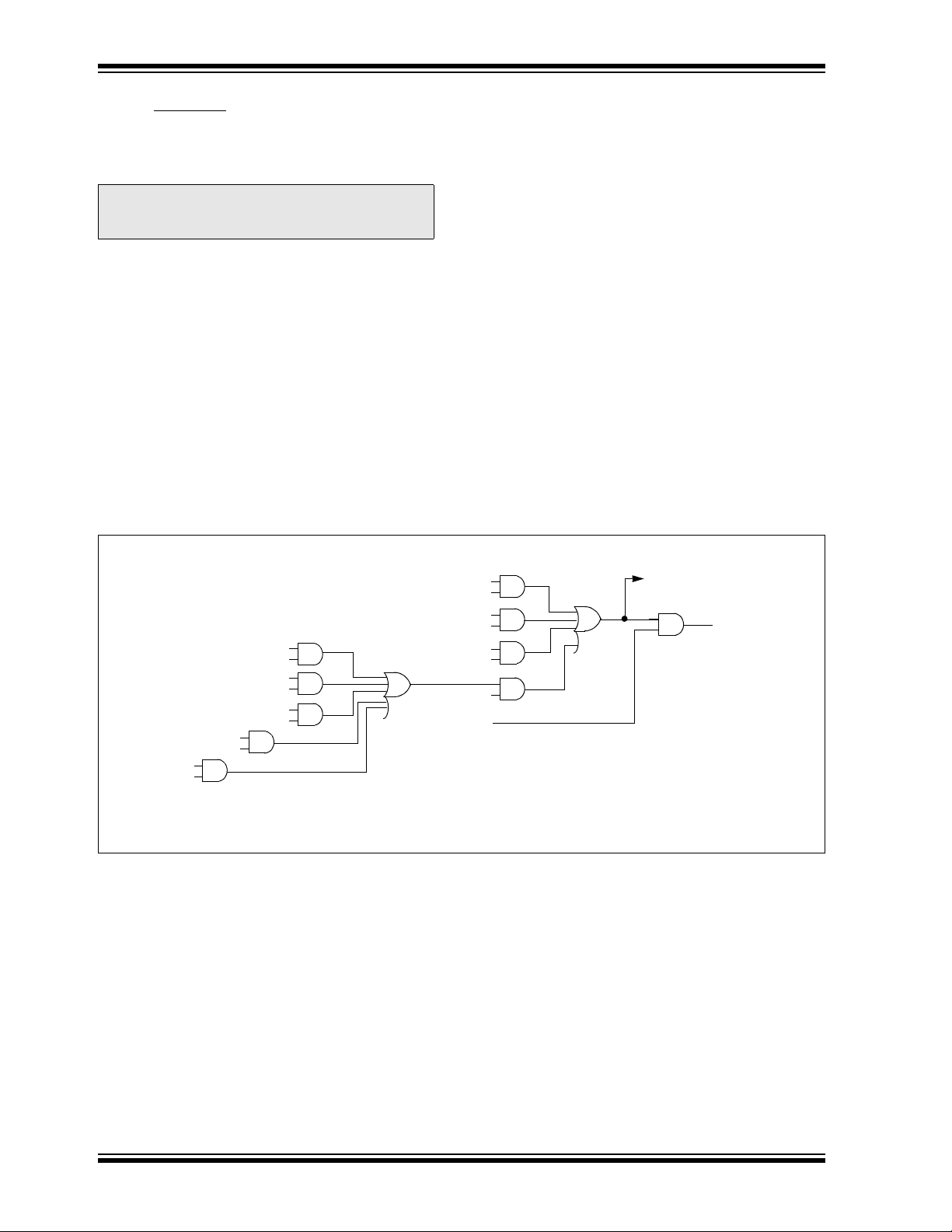
PIC16C62B/72A
ADIF
(1)
ADIE
(1)
SSPIF
SSPIE
CCP1IF
CCP1IE
TMR2IF
TMR2IE
TMR1IF
TMR1IE
T0IF
T0IE
INTF
INTE
RBIF
RBIE
GIE
PEIE
Wake-up (If in SLEEP mode)
Interrupt to CPU
Note 1: The A/D module is not implemented on the PIC16C62B.
10.10 Interrupts
The interrupt control register (INTCON) records individual interrupt requests in flag bits. It also has individual
and global interrupt enable bits.
Note: Individual interrupt flag bits are set regard-
less of the status of their corresponding
mask bit or the GIE bit.
A global interrupt enable bit, GIE (INTCON<7>)
enables or disables all interrupts. When bit GIE is
enabled, and an interrupt’s flag bit and mask bit are set,
the interrupt will vector immediately. Individual interrupts can be disabled through their corresponding
enable bits in various registers. Individual interrupt flag
bits are set regardless of the status of the GIE bit. The
GIE bit is cleared on reset.
The “return from interrupt” instruction, RETFIE, exits
the interrupt routine and sets the GIE bit, which reenables interrupts.
The RB0/INT pin interrupt, the RB port change interrupt
and the TMR0 overflow interrupt flags are contained in
the INTCON register.
FIGURE 10-7: INTERRUPT LOGIC
The peripheral interrupt flags are contained in the special function registers PIR1 and PIR2. The corresponding interrupt enable bits are contained in special
function registers PIE1 and PIE2, and the peripheral
interrupt enable bit is contained in special function register INTCON.
When an interrupt is responded to, the GIE bit is
cleared to disable any further interrupts, the return
address is pushed onto the stack and the PC is loaded
with 0004h. Once in the interrupt service routine, the
source of the interrupt can be determined by polling the
interrupt flag bits. The interrupt flag bit must be cleared
in software before re-enabling interrupts to avoid recursive interrupts.
For external interrupt events, such as the INT pin or
PORTB change interrupt, the interrupt latency will be
three or four instruction cycles, depending on when the
interrupt event occurs. The latency is the same for one
or two cycle instructions. Individual interrupt flag bits
are set regardless of the status of their corresponding
mask bit or the GIE bit
DS35008C-page 62 Preliminary 1998-2013 Microchip Technology Inc.
Page 63

PIC16C62B/72A
10.10.1 INT INTERRUPT
The external interrupt on RB0/INT pin is edge triggered: either rising, if bit INTEDG (OPTION_REG<6>)
is set, or falling, if the INTEDG bit is clear. When a valid
edge appears on the RB0/INT pin, flag bit INTF
(INTCON<1>) is set. This interrupt can be disabled by
clearing enable bit INTE (INTCON<4>). Flag bit INTF
must be cleared in software in the interrupt service routine before re-enabling this interrupt. The INT interrupt
can wake-up the processor from SLEEP, if bit INTE was
set prior to going into SLEEP. The status of global interrupt enable bit GIE decides whether or not the processor branches to the interrupt vector following wake-up.
See Section 10.13 for details on SLEEP mode.
10.10.2 TMR0 INTERRUPT
An overflow (FFh 00h) in the TMR0 register will set
flag bit T0IF (INTCON<2>). The interrupt can be
enabled/disabled by setting/clearing enable bit T0IE
(INTCON<5>). (Section 4.0)
10.10.3 PORTB INTCON CHANGE
An input change on PORTB<7:4> sets flag bit RBIF
(INTCON<0>). The interrupt can be enabled/disabled
by setting/clearing enable bit RBIE (INTCON<4>).
(Section 3.2)
10.11 Context Saving During Interrupts
During an interrupt, only the return PC value is saved
on the stack. Typically, users may wish to save key registers during an interrupt, (i.e., W register and STATUS
register). This will have to be implemented in software.
Example 10-1 stores and restores the W and STATUS
registers. The register, W_TEMP, must be defined in
each bank and must be defined at the same offset from
the bank base address (i.e., if W_TEMP is defined at
0x20 in bank 0, it must also be defined at 0xA0 in bank
1).
The example:
a) Stores the W register.
b) Stores the STATUS register in bank 0.
c) Stores the PCLATH register.
d) Executes the interrupt service routine code
(User-generated).
e) Restores the STATUS register (and bank select
bit).
f) Restores the W and PCLATH registers.
EXAMPLE 10-1: SAVING STATUS, W, AND PCLATH REGISTERS IN RAM
MOVWF W_TEMP ;Copy W to TEMP register, could be bank one or zero
SWAPF STATUS,W ;Swap status to be saved into W
CLRF STATUS ;bank 0, regardless of current bank, Clears IRP,RP1,RP0
MOVWF STATUS_TEMP ;Save status to bank zero STATUS_TEMP register
:
:(ISR)
:
SWAPF STATUS_TEMP,W ;Swap STATUS_TEMP register into W
;(sets bank to original state)
MOVWF STATUS ;Move W into STATUS register
SWAPF W_TEMP,F ;Swap W_TEMP
SWAPF W_TEMP,W ;Swap W_TEMP into W
1998-2013 Microchip Technology Inc. Preliminary DS35008C-page 63
Page 64
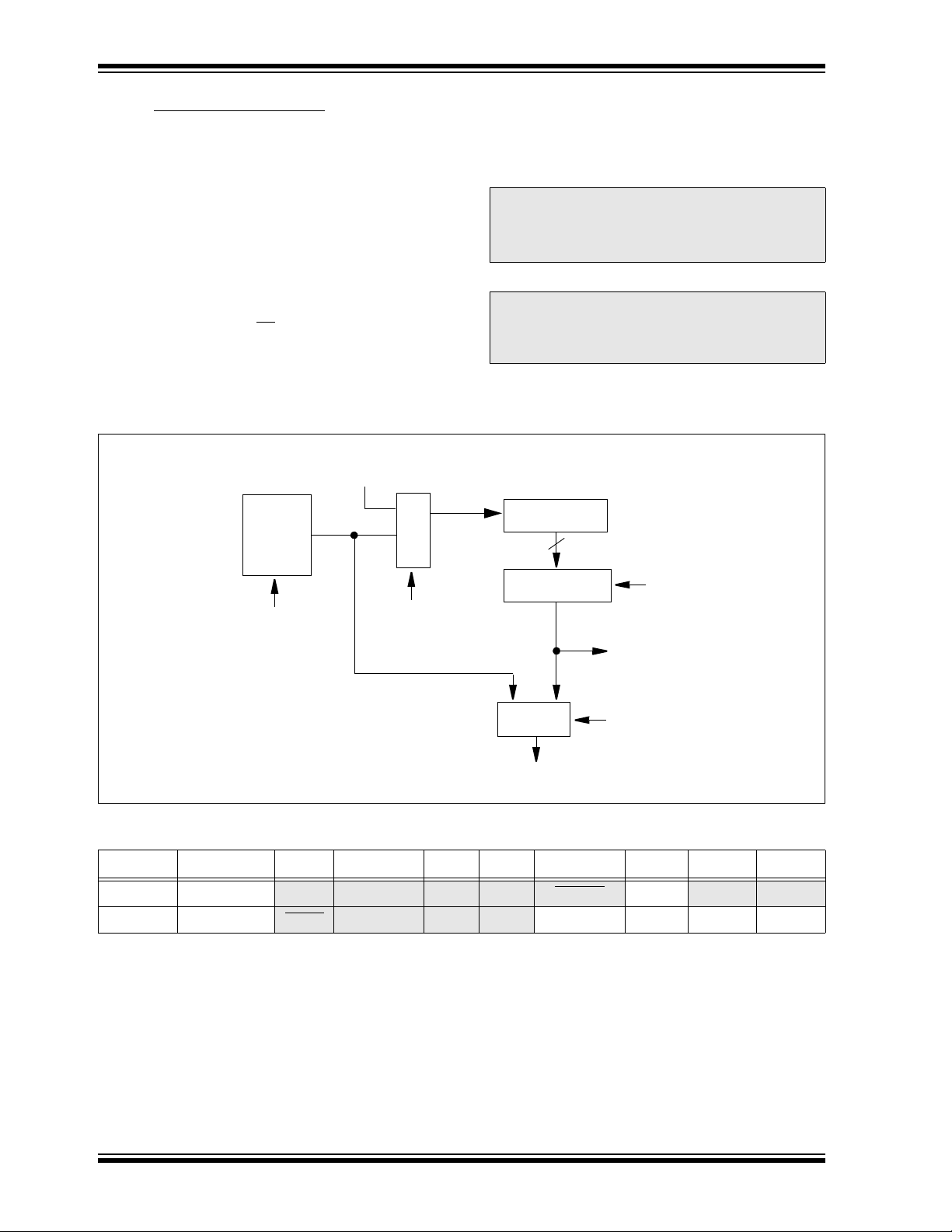
PIC16C62B/72A
From TMR0 Clock Source
(Figure 4-2)
To TMR0 (Figure 4-2)
Postscaler
WDT Timer
WDT
Enable Bit
0
1
M
U
X
PSA
8 - to - 1 MUX
PS2:PS0
0
1
MUX
PSA
WDT
Time-out
Note: PSA and PS2:PS0 are bits in the OPTION_REG register.
8
10.12 Watchdog Timer (WDT)
The Watchdog Timer is a free running on-chip RC oscillator which does not require any external components.
This RC oscillator is separate from the RC oscillator of
the OSC1/CLKIN pin. The WDT will run, even if the
clock on the OSC1/CLKIN and OSC2/CLKOUT pins of
the device has been stopped, for example, by execution
of a SLEEP instruction.
During normal operation, a WDT time-out generates a
device RESET (Watchdog Timer Reset). If the device is
in SLEEP mode, a WDT time-out causes the device to
wake-up and continue with normal operation (Watchdog Timer Wake-up). The TO
bit in the STATUS register
will be cleared upon a Watchdog Timer time-out.
The WDT can be permanently disabled by clearing
configuration bit WDTE (Section 10.1).
FIGURE 10-8: WATCHDOG TIMER BLOCK DIAGRAM
The WDT time-out period (T
WDT, parameter #31) is
multiplied by the prescaler ratio, when the prescaler is
assigned to the WDT. The prescaler assignment
(assigned to either the WDT or Timer0) and prescaler
ratio are set in the OPTION_REG register.
Note: The CLRWDT and SLEEP instructions clear
the WDT and the postscaler, if assigned to
the WDT, and prevent it from timing out and
generating a device RESET condition.
.
Note: When a CLRWDT instruction is executed
and the prescaler is assigned to the WDT,
the prescaler count will be cleared, but the
prescaler assignment is not changed.
FIGURE 10-9: SUMMARY OF WATCHDOG TIMER REGISTERS
Address Name Bit 7 Bit 6 Bit 5 Bit 4 Bit 3 Bit 2 Bit 1 Bit 0
2007h Config. bits
81h
Legend: Shaded cells are not used by the Watchdog Timer.
DS35008C-page 64 Preliminary 1998-2013 Microchip Technology Inc.
OPTION_REG
RBPU INTEDG T0CS T0SE PSA PS2 PS1 PS0
BODEN
CP1 CP0
PWRTE
WDTE FOSC1 FOSC0
Page 65

PIC16C62B/72A
10.13 Power-down Mode (SLEEP)
Power-down mode is entered by executing a SLEEP
instruction.
If enabled, the Watchdog Timer will be cleared but
keeps running, the PD
(STATUS<4>) bit is set, and the oscillator driver is
TO
turned off. The I/O ports maintain the status they had,
before the SLEEP instruction was executed (driving
high, low or hi-impedance).
For lowest current consumption in this mode, place all
I/O pins at either V
cuitry is drawing current from the I/O pin, power-down
the A/D and disable external clocks. Pull all I/O pins
that are hi-impedance inputs, high or low externally, to
avoid switching currents caused by floating inputs. The
T0CKI input should also be at V
current consumption. The contribution from on-chip
pull-ups on PORTB should be considered.
The MCLR
parameter D042).
10.13.1 WAKE-UP FROM SLEEP
The device can wake up from SLEEP through one of
the following events:
1. External reset input on MCLR
2. Watchdog Timer Wake-up (if WDT was
3. Interrupt from INT pin, RB port change, or some
External MCLR
other events are considered a continuation of program
execution and cause a "wake-up". The TO
in the STATUS register can be used to determine the
cause of device reset. The PD bit, which is set on
power-up, is cleared when SLEEP is invoked. The TO
bit is cleared if a WDT time-out occurred (and caused
wake-up).
The following peripheral interrupts can wake the device
from SLEEP:
1. TMR1 interrupt. Timer1 must be operating as
2. CCP capture mode interrupt.
3. Special event trigger (Timer1 in asynchronous
4. SSP (Start/Stop) bit detect interrupt.
5. SSP transmit or receive in slave mode (SPI/I
6. USART RX or TX (synchronous slave mode).
Other peripherals cannot generate interrupts since during SLEEP, no on-chip clocks are present.
When the SLEEP instruction is being executed, the next
instruction (PC + 1) is pre-fetched. For the device to
wake-up through an interrupt event, the corresponding
interrupt enable bit must be set (enabled). Wake-up is
pin must be at a logic high level (VIHMC,
enabled).
Peripheral Interrupts.
an asynchronous counter.
mode using an external clock. CCP1 is in compare mode).
bit (STATUS<3>) is cleared, the
DD or VSS, ensure no external cir-
DD or VSS for lowest
pin.
Reset will cause a device reset. All
and PD bits
2
C).
regardless of the state of the GIE bit. If the GIE bit is
clear (disabled), the device resumes execution at the
instruction after the SLEEP instruction. If the GIE bit is
set (enabled), the device executes the instruction after
the SLEEP instruction and then branches to the interrupt address (0004h). In cases where the execution of
the instruction following SLEEP is not desirable, a NOP
should follow the SLEEP instruction.
10.13.2 WAKE-UP USING INTERRUPTS
When global interrupts are disabled (GIE cleared) and
any interrupt source has both its interrupt enable bit
and interrupt flag bit set, one of the following will occur:
• If the interrupt occurs before the execution of a
SLEEP instruction, the SLEEP instruction will complete as a NOP. Therefore, the WDT and WDT
postscaler will not be cleared, the TO
be set and PD
• If the interrupt occurs during or after the execu-
tion of a SLEEP instruction, the device will immediately wake up from sleep. The SLEEP instruction
will be completely executed before the wake-up.
Therefore, the WDT and WDT postscaler will be
cleared, the TO
be cleared.
Even if the flag bits were checked before executing a
SLEEP instruction, it may be possible for flag bits to
become set before the SLEEP instruction completes. To
determine whether a SLEEP instruction executed, test
bit. If the PD bit is set, the SLEEP instruction
the PD
was executed as a NOP.
To ensure that the WDT is cleared, a CLRWDT instruction should be executed before a SLEEP instruction.
bits will not be cleared.
bit will be set and the PD bit will
bit will not
1998-2013 Microchip Technology Inc. Preliminary DS35008C-page 65
Page 66
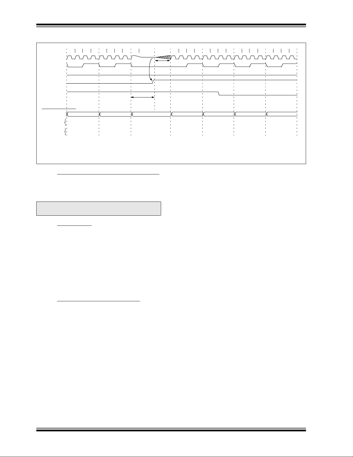
PIC16C62B/72A
Q1 Q2 Q3 Q4 Q1 Q2 Q3 Q4 Q1 Q1 Q2 Q3 Q4 Q1 Q2 Q3 Q4 Q1 Q2 Q3 Q4 Q1 Q2 Q3 Q4
OSC1
CLKOUT(4)
INT pin
INTF flag
(INTCON<1>)
GIE bit
(INTCON<7>)
INSTRUCTION FLOW
PC
Instruction
fetc hed
Instruction
executed
PC PC+1 PC+2
Inst(PC) = SLEEP
Inst(PC - 1)
Inst(PC + 1)
SLEEP
Processor in
SLEEP
Interrupt Latency
(Note 2)
Inst(PC + 2)
Inst(PC + 1)
Inst(0004h)
Inst(0005h)
Inst(0004h)
Dummy cycle
PC + 2 0004h 0005h
Dummy cycle
TOST(2)
PC+2
Note 1: XT, HS or LP oscillator mode assumed.
2: T
OST = 1024TOSC (drawing not to scale) This delay will not be there for RC osc mode.
3: GIE = '1' assumed. In this case after wake- up, the processor jumps to the interrupt routine. If GIE = '0', execution will continue in-line.
4: CLKOUT is not available in these osc modes, but shown here for timing reference.
FIGURE 10-10: WAKE-UP FROM SLEEP THROUGH INTERRUPT
10.14 Program Verification/Code Protection
If the code protection bits have not been programmed,
the on-chip program memory can be read out for verification purposes.
Note: Microchip does not recommend code pro-
tecting windowed devices.
10.15 ID Locations
Four memory locations (2000h - 2003h) are designated
as ID locations where the user can store checksum or
other code-identification numbers. These locations are
not accessible during normal execution, but are readable and writable during program/verify. It is recommended that only the 4 least significant bits of the ID
location are used.
For ROM devices, these values are submitted along
with the ROM code.
10.16 In-Circuit Serial Programming™
PIC16CXXX microcontrollers can be serially programmed while in the end application circuit. This is
simply done with two lines for clock and data, and three
more lines for power, ground and the programming voltage. This allows customers to manufacture boards with
unprogrammed devices, and then program the microcontroller just before shipping the product. This also
allows the most recent firmware or a custom firmware
to be programmed.
For complete details of serial programming, please
refer to the In-Circuit Serial Programming (ICSP™)
Guide, DS30277.
DS35008C-page 66 Preliminary 1998-2013 Microchip Technology Inc.
Page 67
PIC16C62B/72A
Byte-oriented file register operations
13 8 7 6 0
d = 0 for destination W
OPCODE d f (FILE #)
d = 1 for destination f
f = 7-bit file register address
Bit-oriented file register operations
13 10 9 7 6 0
OPCODE b (BIT #) f (FILE #)
b = 3-bit bit address
f = 7-bit file register address
Literal and control operations
13 8 7 0
OPCODE k (literal)
k = 8-bit immediate value
13 11 10 0
OPCODE k (literal)
k = 11-bit immediate value
General
CALL and GOTO instructions only
11.0 INSTRUCTION SET SUMMARY
Each PIC16CXXX instruction is a 14-bit word divided
into an OPCODE which specifies the instruction type
and one or more operands which further specify the
operation of the instruction. The PIC16CXX instruction
set summary in Table 11-2 lists byte-oriented, bit-ori-
ented, and literal and control operations. Table 11-1
shows the opcode field descriptions.
For byte-oriented instructions, 'f' represents a file register designator and 'd' represents a destination designator. The file register designator specifies which file
register is to be used by the instruction.
The destination designator specifies where the result of
the operation is to be placed. If 'd' is zero, the result is
placed in the W register. If 'd' is one, the result is placed
in the file register specified in the instruction.
For bit-oriented instructions, 'b' represents a bit field
designator which selects the number of the bit affected
by the operation, while 'f' represents the number of the
file in which the bit is located.
For literal and control operations, 'k' represents an
eight or eleven bit constant or literal value.
TABLE 11-1 OPCODE FIELD
DESCRIPTIONS
execution time is 1 s. If a conditional test is true or the
program counter is changed as a result of an instruction, the instruction execution time is 2 s.
Table 11-2 lists the instructions recognized by the
MPASM assembler.
Figure 11-1 shows the general formats that the instructions can have.
Note: To maintain upward compatibility with
future PIC16CXXX products, do not use
the OPTION and TRIS instructions.
All examples use the following format to represent a
hexadecimal number:
0xhh
where h signifies a hexadecimal digit.
FIGURE 11-1: GENERAL FORMAT FOR
INSTRUCTIONS
Field Description
f Register file address (0x00 to 0x7F)
W Working register (accumulator)
b Bit address within an 8-bit file register
k Literal field, constant data or label
x Don't care location (= 0 or 1)
The assembler will generate code with x = 0. It is the
recommended form of use for compatibility with all
Microchip software tools.
d Destination select; d = 0: store result in W,
d = 1: store result in file register f.
Default is d = 1
PC Program Counter
Time-out bit
TO
Power-down bit
PD
Z Zero bit
DC Digit Carry bit
C Carry bit
The instruction set is highly orthogonal and is grouped
into three basic categories:
• Byte-oriented operations
• Bit-oriented operations
• Literal and control operations
All instructions are executed within one single instruction cycle, unless a conditional test is true or the program counter is changed as a result of an instruction.
In this case, the execution takes two instruction cycles
with the second cycle executed as a NOP. One instruction cycle consists of four oscillator periods. Thus, for
an oscillator frequency of 4 MHz, the normal instruction
A description of each instruction is available in the
®
PIC
MCU Mid-Range Reference Manual,
(DS33023).
1998-2013 Microchip Technology Inc. Preliminary DS35008C-page 67
Page 68

PIC16C62B/72A
TABLE 11-2 PIC16CXXX INSTRUCTION SET
Mnemonic,
Operands
BYTE-ORIENTED FILE REGISTER OPERATIONS
ADDWF
ANDWF
CLRF
CLRW
COMF
DECF
DECFSZ
INCF
INCFSZ
IORWF
MOVF
MOVWF
NOP
RLF
RRF
SUBWF
SWAPF
XORWF
BIT-ORIENTED FILE REGISTER OPERATIONS
BCF
BSF
BTFSC
BTFSS
LITERAL AND CONTROL OPERATIONS
ADDLW
ANDLW
CALL
CLRWDT
GOTO
IORLW
MOVLW
RETFIE
RETLW
RETURN
SLEEP
SUBLW
XORLW
Note 1: When an I/O register is modified as a function of itself ( e.g., MOVF PORTB, 1), the value used will be that value present
on the pins themselves. For example, if the data latch is '1' for a pin configured as input and is driven low by an external
device, the data will be written back with a '0'.
2: If this instruction is executed on the TMR0 register (and, where applicable, d = 1), the prescaler will be cleared if assigned
to the Timer0 Module.
3: If Program Counter (PC) is modified or a conditional test is true, the instruction requires two cycles. The second cycle is
executed as a NOP.
Description Cycles 14-Bit Opcode Status
MSb LSb
f, d
Add W and f
f, d
AND W with f
f
Clear f
-
Clear W
f, d
Complement f
f, d
Decrement f
f, d
Decrement f, Skip if 0
f, d
Increment f
f, d
Increment f, Skip if 0
f, d
Inclusive OR W with f
f, d
Move f
f
Move W to f
-
No Operation
f, d
Rotate Left f through Carry
f, d
Rotate Right f through Carry
f, d
Subtract W from f
f, d
Swap nibbles in f
f, d
Exclusive OR W with f
f, b
Bit Clear f
f, b
Bit Set f
f, b
Bit Test f, Skip if Clear
f, b
Bit Test f, Skip if Set
k
Add literal and W
k
AND literal with W
k
Call subroutine
-
Clear Watchdog Timer
k
Go to address
k
Inclusive OR literal with W
k
Move literal to W
-
Return from interrupt
k
Return with literal in W
-
Return from Subroutine
-
Go into standby mode
k
Subtract W from literal
k
Exclusive OR literal with W
1
1
1
1
1
1
1(2)
1
1(2)
1
1
1
1
1
1
1
1
1
1
1
1 (2)
1 (2)
1
1
2
1
2
1
1
2
2
2
1
1
1
00
00
00
00
00
00
00
00
00
00
00
00
00
00
00
00
00
00
01
01
01
01
11
11
10
00
10
11
11
00
11
00
00
11
11
0111
0101
0001
0001
1001
0011
1011
1010
1111
0100
1000
0000
0000
1101
1100
0010
1110
0110
00bb
01bb
10bb
11bb
111x
1001
0kkk
0000
1kkk
1000
00xx
0000
01xx
0000
0000
110x
1010
dfff
dfff
lfff
0000
dfff
dfff
dfff
dfff
dfff
dfff
dfff
lfff
0xx0
dfff
dfff
dfff
dfff
dfff
bfff
bfff
bfff
bfff
kkkk
kkkk
kkkk
0110
kkkk
kkkk
kkkk
0000
kkkk
0000
0110
kkkk
kkkk
ffff
ffff
ffff
0011
ffff
ffff
ffff
ffff
ffff
ffff
ffff
ffff
0000
ffff
ffff
ffff
ffff
ffff
ffff
ffff
ffff
ffff
kkkk
kkkk
kkkk
0100
kkkk
kkkk
kkkk
1001
kkkk
1000
0011
kkkk
kkkk
Affected
C,DC,Z
Z
Z
Z
Z
Z
Z
Z
Z
C
C
C,DC,Z
Z
C,DC,Z
Z
,PD
TO
Z
,PD
TO
C,DC,Z
Z
Notes
1,2
1,2
2
1,2
1,2
1,2,3
1,2
1,2,3
1,2
1,2
1,2
1,2
1,2
1,2
1,2
1,2
1,2
3
3
DS35008C-page 68 Preliminary 1998-2013 Microchip Technology Inc.
Page 69

11.1 Instruction Descriptions
PIC16C62B/72A
ADDLW Add Literal and W
label
Syntax: [
] ADDLW k
Operands: 0 k 255
Operation: (W) + k (W)
Status Affected: C, DC, Z
Description:
The contents of the W register are
added to the eight bit literal 'k' and the
result is placed in the W register
ADDWF Add W and f
label
Syntax: [
] ADDWF f,d
Operands: 0 f 127
d
Operation: (W) + (f) (destination)
Status Affected: C, DC, Z
Description:
Add the contents of the W register
with register 'f'. If 'd' is 0, the result is
stored in the W register. If 'd' is 1, the
result is stored back in register 'f'
ANDWF AND W with f
label
Syntax: [
] ANDWF f,d
Operands: 0 f 127
d
Operation: (W) .AND. (f) (destination)
Status Affected: Z
.
Description:
AND the W register with register 'f'. If
'd' is 0, the result is stored in the W
register. If 'd' is 1, the result is stored
back in register 'f'
.
BCF Bit Clear f
Syntax: [
label
] BCF f,b
Operands: 0 f 127
0 b 7
Operation: 0 (f<b>)
Status Affected: None
Description:
Bit 'b' in register 'f' is cleared.
.
ANDLW AND Literal with W
label
Syntax: [
] ANDLW k
Operands: 0 k 255
Operation: (W) .AND. (k) (W)
Status Affected: Z
Description:
The contents of W register are
AND’ed with the eight bit literal 'k'.
The result is placed in the W register
BSF Bit Set f
label
Syntax: [
] BSF f,b
Operands: 0 f 127
0 b 7
Operation: 1 (f<b>)
Status Affected: None
Description:
Bit 'b' in register 'f' is set.
.
1998-2013 Microchip Technology Inc. Preliminary DS35008C-page 69
Page 70

PIC16C62B/72A
BTFSS Bit Test f, Skip if Set
label
Syntax: [
] BTFSS f,b
Operands: 0 f 127
0 b < 7
Operation: skip if (f<b>) = 1
Status Affected: None
Description:
If bit 'b' in register 'f' is '0', then the next
instruction is executed.
If bit 'b' is '1', then the next instruction
is discarded and a NOP is executed
instead, making this a 2T
tion.
BTFSC Bit Test, Skip if Clear
label
Syntax: [
] BTFSC f,b
Operands: 0 f 127
0 b 7
Operation: skip if (f<b>) = 0
Status Affected: None
Description:
If bit 'b' in register 'f' is '1', then the next
instruction is executed.
If bit 'b' in register 'f' is '0', then the next
instruction is discarded, and a NOP is
executed instead, making this a 2T
instruction
.
CY instruc-
CY
CLRF Clear f
label
Syntax: [
] CLRF f
Operands: 0 f 127
Operation: 00h (f)
1 Z
Status Affected: Z
Description:
The contents of register 'f' are cleared
and the Z bit is set.
CLRW Clear W
label
Syntax: [
] CLRW
Operands: None
Operation: 00h (W)
1 Z
Status Affected: Z
Description:
W register is cleared. Zero bit (Z) is
set.
CALL Call Subroutine
label
Syntax: [
] CALL k
Operands: 0 k 2047
Operation: (PC)+ 1 TOS,
k PC<10:0>,
(PCLATH<4:3>) PC<12:11>
Status Affected: None
Description:
DS35008C-page 70 Preliminary 1998-2013 Microchip Technology Inc.
Call Subroutine. First, return address
(PC+1) is pushed onto the stack. The
eleven bit immediate address is loaded
into PC bits <10:0>. The upper bits of
the PC are loaded from PCLATH.
CALL is a two cycle instruction.
CLRWDT Clear Watchdog Timer
label
Syntax: [
] CLRWDT
Operands: None
Operation: 00h WDT
0 WDT prescaler,
1 TO
1 PD
Status Affected: TO, PD
Description:
CLRWDT instruction resets the Watchdog Timer. It also resets the prescaler
of the WDT. Status bits TO
are set.
and PD
Page 71

PIC16C62B/72A
COMF Complement f
label
Syntax: [
] COMF f,d
Operands: 0 f 127
d [0,1]
Operation: (f
) (destination)
Status Affected: Z
Description:
The contents of register 'f' are complemented. If 'd' is 0, the result is stored
in W. If 'd' is 1, the result is stored
back in register 'f'.
DECF Decrement f
label
Syntax: [
] DECF f,d
Operands: 0 f 127
d [0,1]
Operation: (f) - 1 (destination)
Status Affected: Z
Description:
Decrement register 'f'. If 'd' is 0, the
result is stored in the W register. If 'd'
is 1, the result is stored back in regis-
.
ter 'f'
GOTO Unconditional Branch
label
Syntax: [
] GOTO k
Operands: 0 k 2047
Operation: k PC<10:0>
PCLATH<4:3> PC<12:11>
Status Affected: None
Description:
GOTO is an unconditional branch. The
eleven bit immediate value is loaded
into PC bits <10:0>. The upper bits of
PC are loaded from PCLATH<4:3>.
GOTO is a two cycle instruction.
INCF Increment f
label
Syntax: [
] INCF f,d
Operands: 0 f 127
d [0,1]
Operation: (f) + 1 (destination)
Status Affected: Z
Description:
The contents of register 'f' are incremented. If 'd' is 0, the result is placed
in the W register. If 'd' is 1, the result is
placed back in register 'f'.
DECFSZ Decrement f, Skip if 0
label
Syntax: [
] DECFSZ f,d
Operands: 0 f 127
d [0,1]
Operation: (f) - 1 (destination);
skip if result = 0
Status Affected: None
Description:
The contents of register 'f' are decremented. If 'd' is 0, the result is placed in
the W register. If 'd' is 1, the result is
placed back in register 'f'.
If the result is 1, the next instruction, is
executed. If the result is 0, then a NOP is
executed instead making it a 2T
instruction.
CY
INCFSZ Increment f, Skip if 0
label
Syntax: [
] INCFSZ f,d
Operands: 0 f 127
d [0,1]
Operation: (f) + 1 (destination),
skip if result = 0
Status Affected: None
Description:
The contents of register 'f' are incremented. If 'd' is 0, the result is placed
in the W register. If 'd' is 1, the result is
placed back in register 'f'.
If the result is 1, the next instruction is
executed. If the result is 0, a NOP is
executed instead making it a 2T
instruction
.
CY
1998-2013 Microchip Technology Inc. Preliminary DS35008C-page 71
Page 72

PIC16C62B/72A
IORLW Inclusive OR Literal with W
label
Syntax: [
] IORLW k
Operands: 0 k 255
Operation: (W) .OR. k (W)
Status Affected: Z
Description:
The contents of the W register is
OR’ed with the eight bit literal 'k'. The
result is placed in the W register
IORWF Inclusive OR W with f
label
Syntax: [
] IORWF f,d
Operands: 0 f 127
d [0,1]
Operation: (W) .OR. (f) (destination)
Status Affected: Z
Description:
Inclusive OR the W register with register 'f'. If 'd' is 0, the result is placed in
the W register. If 'd' is 1, the result is
placed back in register 'f'.
MOVLW Move Literal to W
label
Syntax: [
] MOVLW k
Operands: 0 k 255
Operation: k (W)
Status Affected: None
Description:
.
The eight bit literal 'k' is loaded into W
. The don’t cares will assem-
register
ble as 0’s.
MOVWF Move W to f
label
Syntax: [
] MOVWF f
Operands: 0 f 127
Operation: (W) (f)
Status Affected: None
Description:
Move data from W register to register
.
'f'
MOVF Move f
label
Syntax: [
] MOVF f,d
Operands: 0 f 127
d [0,1]
Operation: (f) (destination)
Status Affected: Z
Description:
The contents of register f is moved to
a destination dependant upon the status of d. If d = 0, destination is W register. If d = 1, the destination is file
register f itself. d = 1 is useful to test a
file register since status flag Z is
affected.
NOP No Operation
label
Syntax: [
] NOP
Operands: None
Operation: No operation
Status Affected: None
Description:
No operation.
DS35008C-page 72 Preliminary 1998-2013 Microchip Technology Inc.
Page 73

PIC16C62B/72A
Register fC
Register fC
RETFIE Return from Interrupt
label
Syntax: [
] RETFIE
Operands: None
Operation: TOS PC,
1 GIE
Status Affected: None
RETLW Return with Literal in W
label
Syntax: [
] RETLW k
Operands: 0 k 255
Operation: k (W);
TOS PC
Status Affected: None
Description:
The W register is loaded with the eight
bit literal 'k'. The program counter is
loaded from the top of the stack (the
return address). This is a two cycle
instruction.
RLF Rotate Left f through Carry
label
Syntax: [
] RLF f,d
Operands: 0 f 127
d [0,1]
Operation: See description below
Status Affected: C
Description:
The contents of register 'f' are rotated
one bit to the left through the Carry
Flag. If 'd' is 0, the result is placed in
the W register. If 'd' is 1, the result is
stored back in register 'f'.
RRF Rotate Right f through Carry
label
Syntax: [
] RRF f,d
Operands: 0 f 127
d [0,1]
Operation: See description below
Status Affected: C
Description:
The contents of register 'f' are rotated
one bit to the right through the Carry
Flag. If 'd' is 0, the result is placed in
the W register. If 'd' is 1, the result is
placed back in register 'f'.
RETURN Return from Subroutine
label
Syntax: [
] RETURN
Operands: None
Operation: TOS PC
Status Affected: None
Description:
1998-2013 Microchip Technology Inc. Preliminary DS35008C-page 73
Return from subroutine. The stack is
POPed and the top of the stack (TOS)
is loaded into the program counter.
This is a two cycle instruction.
SLEEP
Syntax: [
label
] SLEEP
Operands: None
Operation: 00h WDT,
0 WDT prescaler,
1 TO
,
0 PD
Status Affected: TO, PD
Description:
The power-down status bit, PD is
cleared. Time-out status bit, TO
set. Watchdog Timer and its prescaler are cleared.
The processor is put into SLEEP
mode with the oscillator stopped.
See Section 10.13 for more details.
is
Page 74

PIC16C62B/72A
SUBLW Subtract W from Literal
Syntax: [
label
]SUBLW k
Operands: 0 k 255
Operation: k - (W) W)
Status Affected: C, DC, Z
Description:
The W register is subtracted (2’s complement method) from the eight bit literal 'k'. The result is placed in the W
register.
SUBWF Subtract W from f
Syntax: [
label
]SUBWF f,d
Operands: 0 f 127
d [0,1]
Operation: (f) - (W) destination)
Status
C, DC, Z
Affected:
Description:
Subtract (2’s complement method) W
register from register 'f'. If 'd' is 0, the
result is stored in the W register. If 'd' is
1, the result is stored back in register 'f'.
XORLW Exclusive OR Literal with W
Syntax: [
label
]XORLW k
Operands: 0 k 255
Operation: (W) .XOR. k W)
Status Affected: Z
Description:
The contents of the W register are
XOR’ed with the eight bit literal 'k'.
The result is placed in the W register.
XORWF Exclusive OR W with f
label
Syntax: [
] XORWF f,d
Operands: 0 f 127
d [0,1]
Operation: (W) .XOR. (f) destination)
Status Affected: Z
Description:
Exclusive OR the contents of the W
register with register 'f'. If 'd' is 0, the
result is stored in the W register. If 'd'
is 1, the result is stored back in register 'f'.
SWAPF Swap Nibbles in f
label
Syntax: [
] SWAPF f,d
Operands: 0 f 127
d [0,1]
Operation: (f<3:0>) (destination<7:4>),
(f<7:4>) (destination<3:0>)
Status Affected: None
Description:
The upper and lower nibbles of register 'f' are exchanged. If 'd' is 0, the
result is placed in W register. If 'd' is 1,
the result is placed in register 'f'.
DS35008C-page 74 Preliminary 1998-2013 Microchip Technology Inc.
Page 75

PIC16C62B/72A
12.0 DEVELOPMENT SUPPORT
The PIC® microcontrollers are supported with a full
range of hardware and software development tools:
• Integrated Development Environment
- MPLAB™ IDE Software
• Assemblers/Compilers/Linkers
- MPASM Assembler
- MPLAB-C17 and MPLAB-C18 C Compilers
- MPLINK/MPLIB Linker/Librarian
• Simulators
- MPLAB-SIM Software Simulator
•Emulators
- MPLAB-ICEReal-Time In-Circuit Emulator
- PICMASTER
Emulator
- ICEPIC™
• In-Circuit Debugger
- MPLAB-ICD for PIC16F877
• Device Programmers
-PRO MATE
- PICSTART Plus Entry-Level Prototype
Programmer
• Low-Cost Demonstration Boards
- SIMICE
- PICDEM-1
- PICDEM-2
- PICDEM-3
- PICDEM-17
- SEEVAL
-KEELOQ
12.1 MPLAB Integrated Development
Environment Software
- The MPLAB IDE software brings an ease of
software development previously unseen in
the 8-bit microcontroller market. MPLAB is a
Windows
• Multiple functionality
-editor
- simulator
- programmer (sold separately)
- emulator (sold separately)
• A full featured editor
• A project manager
• Customizable tool bar and key mapping
• A status bar
• On-line help
®
/PICMASTER-CE In-Circuit
II Universal Programmer
-based application which contains:
MPLAB allows you to:
• Edit your source files (either assembly or ‘C’)
• One touch assemble (or compile) and download
to PIC MCU tools (automatically updates all project information)
• Debug using:
- source files
- absolute listing file
- object code
The ability to use MPLAB with Microchip’s simulator,
MPLAB-SIM, allows a consistent platform and the ability to easily switch from the cost-effective simulator to
the full featured emulator with minimal retraining.
12.2 MPASM Assembler
MPASM is a full featured universal macro assembler for
all PIC MCUs. It can produce absolute code directly in
the form of HEX files for device programmers, or it can
generate relocatable objects for MPLINK.
MPASM has a command line interface and a Windows
shell and can be used as a standalone application on a
Windows 3.x or greater system. MPASM generates
relocatable object files, Intel standard HEX files, MAP
files to detail memory usage and symbol reference, an
absolute LST file which contains source lines and generated machine code, and a COD file for MPLAB
debugging.
MPASM features include:
• MPASM and MPLINK are integrated into MPLAB
projects.
• MPASM allows user defined macros to be created
for streamlined assembly.
• MPASM allows conditional assembly for multi purpose source files.
• MPASM directives allow complete control over the
assembly process.
12.3 MPLAB-C17 and MPLAB-C18
C Compilers
The MPLAB-C17 and MPLAB-C18 Code Development
Systems are complete ANSI ‘C’ compilers and integrated development environments for Microchip’s
PIC17CXXX and PIC18CXXX family of microcontrollers, respectively. These compilers provide powerful
integration capabilities and ease of use not found with
other compilers.
For easier source level debugging, the compilers provide symbol information that is compatible with the
MPLAB IDE memory display.
12.4 MPLINK/MPLIB Linker/Librarian
MPLINK is a relocatable linker for MPASM and
MPLAB-C17 and MPLAB-C18. It can link relocatable
objects from assembly or C source files along with precompiled libraries using directives from a linker script.
1998-2013 Microchip Technology Inc. Preliminary DS35008C-page 75
Page 76

PIC16C62B/72A
MPLIB is a librarian for pre-compiled code to be used
with MPLINK. When a routine from a library is called
from another source file, only the modules that contains
that routine will be linked in with the application. This
allows large libraries to be used efficiently in many different applications. MPLIB manages the creation and
modification of library files.
MPLINK features include:
• MPLINK works with MPASM and MPLAB-C17
and MPLAB-C18.
• MPLINK allows all memory areas to be defined as
sections to provide link-time flexibility.
MPLIB features include:
• MPLIB makes linking easier because single libraries can be included instead of many smaller files.
• MPLIB helps keep code maintainable by grouping
related modules together.
• MPLIB commands allow libraries to be created
and modules to be added, listed, replaced,
deleted, or extracted.
12.5 MPLAB-SIM Software Simulator
The MPLAB-SIM Software Simulator allows code
development in a PC host environment by simulating
the PIC series microcontrollers on an instruction level.
On any given instruction, the data areas can be examined or modified and stimuli can be applied from a file
or user-defined key press to any of the pins. The execution can be performed in single step, execute until
break, or trace mode.
MPLAB-SIM fully supports symbolic debugging using
MPLAB-C17 and MPLAB-C18 and MPASM. The Software Simulator offers the flexibility to develop and
debug code outside of the laboratory environment making it an excellent multi-project software development
tool.
12.6 MPLAB-ICE High Performance
Universal In-Circuit Emulator with
MPLAB IDE
The MPLAB-ICE Universal In-Circuit Emulator is
intended to provide the product development engineer
with a complete microcontroller design tool set for PIC
microcontrollers (MCUs). Software control of MPLABICE is provided by the MPLAB Integrated Development
Environment (IDE), which allows editing, “make” and
download, and source debugging from a single environment.
Interchangeable processor modules allow the system
to be easily reconfigured for emulation of different processors. The universal architecture of the MPLAB-ICE
allows expansion to support new PIC microcontrollers.
The MPLAB-ICE Emulator System has been designed
as a real-time emulation system with advanced features that are generally found on more expensive devel-
®
opment tools. The PC platform and Microsoft
3.x/95/98 environment were chosen to best make these
features available to you, the end user.
MPLAB-ICE 2000 is a full-featured emulator system
with enhanced trace, trigger, and data monitoring features. Both systems use the same processor modules
and will operate across the full operating speed range
of the PIC MCU.
Windows
12.7 PICMASTER/PICMASTER CE
The PICMASTER system from Microchip Technology is
a full-featured, professional quality emulator system.
This flexible in-circuit emulator provides a high-quality,
universal platform for emulating Microchip 8-bit PIC
microcontrollers (MCUs). PICMASTER systems are
sold worldwide, with a CE compliant model available for
European Union (EU) countries.
12.8 ICEPIC
ICEPIC is a low-cost in-circuit emulation solution for the
Microchip Technology PIC16C5X, PIC16C6X,
PIC16C7X, and PIC16CXXX families of 8-bit one-timeprogrammable (OTP) microcontrollers. The modular
system can support different subsets of PIC16C5X or
PIC16CXXX products through the use of
interchangeable personality modules or daughter
boards. The emulator is capable of emulating without
target application circuitry being present.
12.9 MPLAB-ICD In-Circuit Debugger
Microchip's In-Circuit Debugger, MPLAB-ICD, is a powerful, low-cost run-time development tool. This tool is
based on the flash PIC16F877 and can be used to
develop for this and other PIC microcontrollers from the
PIC16CXXX family. MPLAB-ICD utilizes the In-Circuit
Debugging capability built into the PIC16F87X. This
feature, along with Microchip's In-Circuit Serial Programming protocol, offers cost-effective in-circuit flash
programming and debugging from the graphical user
interface of the MPLAB Integrated Development Environment. This enables a designer to develop and
debug source code by watching variables, single-stepping and setting break points. Running at full speed
enables testing hardware in real-time. The MPLAB-ICD
is also a programmer for the flash PIC16F87X family.
12.10 PRO MATE II Universal Programmer
The PRO MATE II Universal Programmer is a full-featured programmer capable of operating in stand-alone
mode as well as PC-hosted mode. PRO MATE II is CE
compliant.
The PRO MATE II has programmable V
supplies which allows it to verify programmed memory
DD min and VDD max for maximum reliability. It has
at V
an LCD display for instructions and error messages,
keys to enter commands and a modular detachable
socket assembly to support various package types. In
DD and VPP
DS35008C-page 76 Preliminary 1998-2013 Microchip Technology Inc.
Page 77

PIC16C62B/72A
stand-alone mode the PRO MATE II can read, verify or
program PIC devices. It can also set code-protect bits
in this mode.
12.11 PICSTART Plus Entry Level
Development System
The PICSTART programmer is an easy-to-use, lowcost prototype programmer. It connects to the PC via
one of the COM (RS-232) ports. MPLAB Integrated
Development Environment software makes using the
programmer simple and efficient.
PICSTART Plus supports all PIC devices with up to 40
pins. Larger pin count devices such as the PIC16C92X,
and PIC17C76X may be supported with an adapter
socket. PICSTART Plus is CE compliant.
12.12 SIMICE Entry-Level
Hardware Simulator
SIMICE is an entry-level hardware development system designed to operate in a PC-based environment
with Microchip’s simulator MPLAB-SIM. Both SIMICE
and MPLAB-SIM run under Microchip Technology’s
MPLAB Integrated Development Environment (IDE)
software. Specifically, SIMICE provides hardware simulation for Microchip’s PIC12C5XX, PIC12CE5XX, and
PIC16C5X families of PIC 8-bit microcontrollers. SIMICE works in conjunction with MPLAB-SIM to provide
non-real-time I/O port emulation. SIMICE enables a
developer to run simulator code for driving the target
system. In addition, the target system can provide input
to the simulator code. This capability allows for simple
and interactive debugging without having to manually
generate MPLAB-SIM stimulus files. SIMICE is a valuable debugging tool for entry-level system development.
12.13 PICDEM-1 Low-Cost PIC MCU
Demonstration Board
The PICDEM-1 is a simple board which demonstrates
the capabilities of several of Microchip’s microcontrollers. The microcontrollers supported are: PIC16C5X
(PIC16C54 to PIC16C58A), PIC16C61, PIC16C62X,
PIC16C71, PIC16C8X, PIC17C42, PIC17C43 and
PIC17C44. All necessary hardware and software is
included to run basic demo programs. The users can
program the sample microcontrollers provided with
the PICDEM-1 board, on a PRO MATE II or
PICSTART-Plus programmer, and easily test firmware. The user can also connect the PICDEM-1
board to the MPLAB-ICE emulator and download the
firmware to the emulator for testing. Additional prototype area is available for the user to build some additional hardware and connect it to the microcontroller
socket(s). Some of the features include an RS-232
interface, a potentiometer for simulated analog input,
push-button switches and eight LEDs connected to
PORTB.
12.14 PICDEM-2 Low-Cost PIC16CXX
Demonstration Board
The PICDEM-2 is a simple demonstration board that
supports the PIC16C62, PIC16C64, PIC16C65,
PIC16C73 and PIC16C74 microcontrollers. All the
necessary hardware and software is included to
run the basic demonstration programs. The user
can program the sample microcontrollers provided
with the PICDEM-2 board, on a PRO MATE II programmer or PICSTART-Plus, and easily test firmware.
The MPLAB-ICE emulator may also be used with the
PICDEM-2 board to test firmware. Additional prototype
area has been provided to the user for adding additional hardware and connecting it to the microcontroller
socket(s). Some of the features include a RS-232 interface, push-button switches, a potentiometer for simulated analog input, a Serial EEPROM to demonstrate
usage of the I
tion to an LCD module and a keypad.
2
C bus and separate headers for connec-
12.15 PICDEM-3 Low-Cost PIC16CXXX
Demonstration Board
The PICDEM-3 is a simple demonstration board that
supports the PIC16C923 and PIC16C924 in the PLCC
package. It will also support future 44-pin PLCC
microcontrollers with a LCD Module. All the necessary hardware and software is included to run the
basic demonstration programs. The user can program the sample microcontrollers provided with
the PICDEM-3 board, on a PRO MATE II programmer or PICSTART Plus with an adapter socket, and
easily test firmware. The MPLAB-ICE emulator may
also be used with the PICDEM-3 board to test firmware. Additional prototype area has been provided to
the user for adding hardware and connecting it to the
microcontroller socket(s). Some of the features include
an RS-232 interface, push-button switches, a potentiometer for simulated analog input, a thermistor and
separate headers for connection to an external LCD
module and a keypad. Also provided on the PICDEM-3
board is an LCD panel, with 4 commons and 12 segments, that is capable of displaying time, temperature
and day of the week. The PICDEM-3 provides an additional RS-232 interface and Windows 3.1 software for
showing the demultiplexed LCD signals on a PC. A simple serial interface allows the user to construct a hardware demultiplexer for the LCD signals.
12.16 PICDEM-17
The PICDEM-17 is an evaluation board that demonstrates the capabilities of several Microchip microcontrollers, including PIC17C752, PIC17C756,
PIC17C762, and PIC17C766. All necessary hardware
is included to run basic demo programs, which are supplied on a 3.5-inch disk. A programmed sample is
included, and the user may erase it and program it with
the other sample programs using the PRO MATE II or
PICSTART Plus device programmers and easily debug
1998-2013 Microchip Technology Inc. Preliminary DS35008C-page 77
Page 78

PIC16C62B/72A
and test the sample code. In addition, PICDEM-17 supports down-loading of programs to and executing out of
external FLASH memory on board. The PICDEM-17 is
also usable with the MPLAB-ICE or PICMASTER emulator, and all of the sample programs can be run and
modified using either emulator. Additionally, a generous prototype area is available for user hardware.
12.17 SEEVAL Evaluation and Programming
System
The SEEVAL SEEPROM Designer’s Kit supports all
Microchip 2-wire and 3-wire Serial EEPROMs. The kit
includes everything necessary to read, write, erase or
program special features of any Microchip SEEPROM
product including Smart Serials and secure serials.
The Total Endurance Disk is included to aid in tradeoff analysis and reliability calculations. The total kit can
significantly reduce time-to-market and result in an
optimized system.
12.18 KEELOQ Evaluation and
Programming Tools
KEELOQ evaluation and programming tools support
Microchips HCS Secure Data Products. The HCS evaluation kit includes an LCD display to show changing
codes, a decoder to decode transmissions, and a programming interface to program test transmitters.
DS35008C-page 78 Preliminary 1998-2013 Microchip Technology Inc.
Page 79

TABLE 12-1: DEVELOPMENT TOOLS FROM MICROCHIP
PIC12CXXX
PIC14000
PIC16C5X
PIC16C6X
PIC16CXXX
PIC16F62X
PIC16C7X
PIC16C7XX
PIC16C8X
PIC16F8XX
PIC16C9XX
PIC17C4X
PIC17C7XX
PIC18CXX2
24CXX/
25CXX/
93CXX
HCSXXX
MCRFXXX
MCP2510
Software Tools
MPLABIntegrated
Development Environment
MPLAB C17 Compiler
MPLAB C18 Compiler
MPASM/MPLINK
Emulators
MPLAB™-ICE
**
PICMASTER/PICMASTER-CE
ICEPICLow-Cost
In-Circuit Emulator
Debugger
MPLAB-ICD In-Circuit Debugger
*
*
Programmers
PICSTART
Plus
Low-Cost Universal Dev. Kit
**
PRO MATE
II
Universal Programmer
**
Demo Boards and Eval Kits
SIMICE
PICDEM-1
†
PICDEM-2
†
†
PICDEM-3PICDEM-14APICDEM-17K
EELOQ
®
Evaluation Kit
K
EELOQ Transponder Kit
microID™ Programmer’s Kit125 kHz microID Developer’s Kit125 kHz Anticollision microID
Developer’s Kit13.56 MHz Anticollision microID
Developer’s KitMCP2510 CAN Developer’s Kit
* Contact the Microchip Technology Inc. web site at www.microchip.com for information on how to use the MPLAB-ICD In-Circuit Debugger (DV164001) with PIC16C62, 63, 64, 65, 72, 73, 74, 76, 77
** Contact Microchip Technology Inc. for availability date.
†
Development tool is available on select devices.
PIC16C62B/72A
1998-2013 Microchip Technology Inc. Preliminary DS35008C-page 79
Page 80

PIC16C62B/72A
NOTES:
DS35008C-page 80 Preliminary 1998-2013 Microchip Technology Inc.
Page 81

PIC16C62B/72A
13.0 ELECTRICAL CHARACTERISTICS
Absolute Maximum Ratings
Ambient temperature under bias.............................................................................................................-55°C to +125°C
Storage temperature.............................................................................................................................. -65°C to +150°C
Voltage on any pin with respect to V
Voltage on V
Voltage on MCLR
DD with respect to VSS ......................................................................................................... -0.3V to +7.5V
with respect to VSS (Note 2).......................................................................................... 0V to +13.25V
Voltage on RA4 with respect to Vss............................................................................................................... 0V to +8.5V
Total power dissipation (Note 1)................................................................................................................................1.0W
Maximum current out of V
Maximum current into V
Input clamp current, I
IK (VI < 0 or VI > VDD) 20 mA
Output clamp current, I
Maximum output current sunk by any I/O pin..........................................................................................................25 mA
Maximum output current sourced by any I/O pin ....................................................................................................25 mA
Maximum current sunk byPORTA and PORTB (combined) .................................................................................200 mA
Maximum current sourced by PORTA and PORTB (combined)............................................................................200 mA
Maximum current sunk by PORTC........................................................................................................................200 mA
Maximum current sourced by PORTC ..................................................................................................................200 mA
Note 1: Power dissipation is calculated as follows: Pdis = V
2: Voltage spikes below V
Thus, a series resistor of 50-100 should be used when applying a “low” level to the MCLR/
than pulling this pin directly to V
† NOTICE: Stresses above those listed under “Absolute Maximum Ratings” may cause permanent damage to the
device. This is a stress rating only and functional operation of the device at those or any other conditions above those
indicated in the operation listings of this specification is not implied. Exposure to maximum rating conditions for
extended periods may affect device reliability.
(†)
SS (except VDD, MCLR, and RA4).......................................... -0.3V to (VDD + 0.3V)
SS pin ...........................................................................................................................300 mA
DD pin ..............................................................................................................................250 mA
OK (VO < 0 or VO > VDD) 20 mA
DD x {IDD - IOH} + {(VDD-VOH) x IOH} + (VOl x IOL)
SS at the MCLR/VPP pin, inducing currents greater than 80 mA, may cause latch-up.
VPP pin, rather
SS.
1998-2013 Microchip Technology Inc. Preliminary DS35008C-page 81
Page 82

PIC16C62B/72A
Frequency
Volt ag e
6.0 V
5.5 V
4.5 V
4.0 V
2.0 V
20 MHz
5.0 V
3.5 V
3.0 V
2.5 V
PIC16CXXX
PIC16CXXX-20
Frequency
Volt ag e
6.0 V
5.5 V
4.5 V
4.0 V
2.0 V
10 MHz
5.0 V
3.5 V
3.0 V
2.5 V
FMAX = (12.0 MHz/V) (VDDAPPMIN - 2.5 V) + 4 MHz
Note: VDDAPPMIN is the minimum voltage of the PIC® device in the application.
4 MHz
PIC16LCXXX-04
Fmax is no greater than 10 MHz.
FIGURE 13-1: PIC16C62B/72A-20 VOLTAGE-FREQUENCY GRAPH
FIGURE 13-2: PIC16LC62B/72A AND PIC16C62B/72A/JW VOLTAGE-FREQUENCY GRAPH
DS35008C-page 82 Preliminary 1998-2013 Microchip Technology Inc.
Page 83

PIC16C62B/72A
Frequency
Volt age
6.0 V
5.5 V
4.5 V
4.0 V
2.0 V
5.0 V
3.5 V
3.0 V
2.5 V
PIC16CXXX-04
4 MHz
FIGURE 13-3: PIC16C62B/72A-04 VOLTAGE-FREQUENCY GRAPH
1998-2013 Microchip Technology Inc. Preliminary DS35008C-page 83
Page 84

PIC16C62B/72A
13.1 DC Characteristics: PIC16C62B/72A-04 (Commercial, Industrial, Extended)
PIC16C62B/72A-20 (Commercial, Industrial, Extended)
Standard Operating Conditions (unless otherwise stated)
DC CHARACTERISTICS
Param
Sym Characteristic Min Typ† Max Units Conditions
No.
D001
V
DD Supply Voltage 4.0
D001A
D002* V
DR RAM Data Retention
Vol tag e (Note 1)
D003 V
POR VDD Start Voltage to
ensure internal
Power-on Reset signal
D004*
D004A*
SVDD VDD Rise Rate to
ensure internal
Power-on Reset signal
D005 V
BOR Brown-out Reset
voltage trip point
D010
I
DD Supply Current
(Note 2, 5)
Operating temperature 0°C T
-40°C T
-40°C T
-
4.5
BOR*
V
5.5
-
5.5
-
5.5
V
V
V
-1.5- V
-VSS - V See section on Power-on Reset for details
0.05
--V/ms PWRT enabled (PWRTE bit clear)
TBD--
3.65 - 4.35 V BODEN bit set
-
2.7
A +70°C for commercial
A +85°C for industrial
A +125°C for extended
XT, RC and LP osc mode
HS osc mode
BOR enabled (Note 7)
PWRT disabled (PWRTE
See section on Power-on Reset for details
XT, RC osc modes
OSC = 4 MHz, VDD = 5.5V (Note 4)
F
bit set)
D013
D020
D021
D021B
I
PD Power-down Current
(Note 3, 5)
-
10520mAmA
-
10.5
-
1.5
-
1.5
-
2.5
42
16
19
19
HS osc mode
OSC = 20 MHz, VDD = 5.5V
F
A
VDD = 4.0V, WDT enabled,-40C to +85C
DD = 4.0V, WDT disabled, 0C to +70C
A
V
DD = 4.0V, WDT disabled,-40C to +85C
V
A
V
DD = 4.0V, WDT disabled,-40C to +125C
A
Module Differential
Current (Note 6)
D022*
D022A*
IWDT
IBOR
Watchdog Timer
Brown-out Reset
-
6.0
-
TBD20200AA
WDTE BIT SET, VDD = 4.0V
BODEN bit set, V
DD = 5.0V
* These parameters are characterized but not tested.
† Data in "Typ" column is at 5V, 25°C unless otherwise stated. These parameters are for design guidance only
and are not tested.
Note 1: This is the limit to which V
DD can be lowered without losing RAM data.
2: The supply current is mainly a function of the operating voltage and frequency. Other factors such as I/O pin
loading and switching rate, oscillator type, internal code execution pattern, and temperature also have an
impact on the current consumption.
The test conditions for all I
OSC1 = external square wave, from rail to rail; all I/O pins tristated, pulled to V
= VDD; WDT enabled/disabled as specified.
MCLR
DD measurements in active operation mode are:
DD,
3: The power-down current in SLEEP mode does not depend on the oscillator type. Power-down current is
measured with the part in SLEEP mode, with all I/O pins in hi-impedance state and tied to V
DD and VSS.
4: For RC osc mode, current through Rext is not included. The current through the resistor can be estimated by
the formula Ir = VDD/2Rext (mA) with Rext in kOhm.
5: Timer1 oscillator (when enabled) adds approximately 20 A to the specification. This value is from charac-
terization and is for design guidance only. This is not tested.
6: The current is the additional current consumed when this peripheral is enabled. This current should be
added to the base I
DD or IPD measurement.
7: This is the voltage where the device enters the Brown-out Reset. When BOR is enabled, the device will
perform a brown-out reset when V
DD falls below VBOR.
DS35008C-page 84 Preliminary 1998-2013 Microchip Technology Inc.
Page 85

PIC16C62B/72A
13.2 DC Characteristics: PIC16LC62B/72A-04 (Commercial, Industrial)
Standard Operating Conditions (unless otherwise stated)
DC CHARACTERISTICS
Param
Sym Characteristic Min Typ† Max Units Conditions
No.
D001 V
D002* V
DD Supply Voltage 2.5
DR RAM Data Retention
Vol tag e (Note 1)
D003 V
POR VDD Start Voltage to
ensure internal
Power-on Reset signal
D004*
D004A*
SVDD VDD Rise Rate to
ensure internal
Power-on Reset signal
D005 V
BOR Brown-out Reset
voltage trip point
D010
I
DD Supply Current
(Note 2, 5)
Operating temperature 0°C TA +70°C for commercial
A +85°C for industrial
LP, XT, RC osc modes (DC - 4 MHz)
BOR enabled (Note 7)
V
BOR*
-
-
-40°C T
5.5
5.5VV
-1.5- V
-VSS - V See section on Power-on Reset for details
0.05
TBD
-
--V/ms PWRT enabled (PWRTE bit clear)
-
PWRT disabled (PWRTE
See section on Power-on Reset for details
3.65 - 4.35 V BODEN bit set
-
2.0
3.848mAAXT, RC osc modes
OSC = 4 MHz, VDD = 3.0V (Note 4)
F
bit set)
D010A
-
22.5
LP OSC MODE
FOSC = 32 kHz, VDD = 3.0V, WDT disabled
D020
D021
D021A
PD Power-down Current
I
(Note 3, 5)
-
7.5
-
0.9
-
0.9
30
5
5
DD = 3.0V, WDT enabled, -40C to +85C
A
V
DD = 3.0V, WDT disabled, 0C to +70C
V
A
DD = 3.0V, WDT disabled, -40C to +85C
V
A
Module Differential
Current (Note 6)
D022*
D022A*
IWDT
IBOR
Watchdog Timer
Brown-out Reset
-
6.0
-
TBD20200AA
BIT SET, VDD = 4.0V
WDTE
BODEN bit set, V
DD = 5.0V
* These parameters are characterized but not tested.
† Data in "Typ" column is at 5V, 25°C unless otherwise stated. These parameters are for design guidance only
and are not tested.
Note 1: This is the limit to which V
DD can be lowered without losing RAM data.
2: The supply current is mainly a function of the operating voltage and frequency. Other factors such as I/O pin
loading and switching rate, oscillator type, internal code execution pattern, and temperature also have an
impact on the current consumption.
The test conditions for all I
OSC1 = external square wave, from rail to rail; all I/O pins tristated, pulled to V
= VDD; WDT enabled/disabled as specified.
MCLR
DD measurements in active operation mode are:
DD,
3: The power-down current in SLEEP mode does not depend on the oscillator type. Power-down current is
measured with the part in SLEEP mode, with all I/O pins in hi-impedance state and tied to V
DD and VSS.
4: For RC osc mode, current through Rext is not included. The current through the resistor can be estimated by
the formula Ir = V
DD/2Rext (mA) with Rext in kOhm.
5: Timer1 oscillator (when enabled) adds approximately 20 A to the specification. This value is from charac-
terization and is for design guidance only. This is not tested.
6: The current is the additional current consumed when this peripheral is enabled. This current should be
added to the base IDD or IPD measurement.
7: This is the voltage where the device enters the Brown-out Reset. When BOR is enabled, the device will
perform a brown-out reset when V
DD falls below VBOR.
1998-2013 Microchip Technology Inc. Preliminary DS35008C-page 85
Page 86

PIC16C62B/72A
13.3 DC Characteristics: PIC16C62B/72A-04 (Commercial, Industrial, Extended)
PIC16C62B/72A-20 (Commercial, Industrial, Extended)
PIC16LC62B/72A-04 (Commercial, Industrial)
Standard Operating Conditions (unless otherwise stated)
Operating temperature 0°C T
DC CHARACTERISTICS
Operating voltage V
and Section 13.2
Param
Sym Characteristic Min Typ† Max Units Conditions
No.
Input Low Voltage
IL I/O ports
V
D030
with TTL buffer VSS
D030A
D031 with Schmitt Trigger buffer V
D032 MCLR
, OSC1 (in RC mode) Vss - 0.2VDD V
D033 OSC1 (in XT, HS and LP
Vss
SS -0.2VDD V
Vss - 0.3VDD V Note1
--0.15V
modes)
Input High Voltage
V
IH I/O ports -
D040 with TTL buffer 2.0 - V
D040A 0.25VD
D
+ 0.8V
- Vdd V For entire V
-40°C T
-40°C T
DD range as described in DC spec Section 13.1
DD
0.8V
DD V4.5V VDD 5.5V
A +70°C for commercial
A +85°C for industrial
A +125°C for extended
VVFor entire V
4.5V V
DD range
DD 5.5V
DD range
D041 with Schmitt Trigger buffer 0.8VDD -VDD V For entire VDD range
D042 MCLR 0.8VDD -VDD V
D042A OSC1 (XT, HS and LP modes) 0.7V
DD -VDD V Note1
D043 OSC1 (in RC mode) 0.9VDD -VddV
Input Leakage Current
(Notes 2, 3)
D060 I
IL I/O ports - - 1 AVss VPIN VDD,
Pin at hi-impedance
D061 MCLR
, RA4/T0CKI - - 5 AVss VPIN VDD
D063 OSC1 - - 5 AVss VPIN VDD,
XT, HS and LP osc modes
D070 I
PURB PORTB weak pull-up current 50 250 400 AVDD = 5V, VPIN = VSS
Output Low Voltage
D080 V
OL I/O ports - - 0.6 V IOL = 8.5 mA, VDD = 4.5V,
-40C to +85C
* These parameters are characterized but not tested.
† Data in “Typ” column is at 5V, 25C unless otherwise stated. These parameters are for design guidance only
and are not tested.
Note 1: In RC oscillator mode, the OSC1/CLKIN pin is a Schmitt Trigger input. It is not recommended that the
device be driven with external clock in RC mode.
2: The leakage current on the MCLR
/VPP pin is strongly dependent on the applied voltage level. The specified
levels represent normal operating conditions. Higher leakage current may be measured at different input voltages.
3: Negative current is defined as current sourced by the pin.
DS35008C-page 86 Preliminary 1998-2013 Microchip Technology Inc.
Page 87

PIC16C62B/72A
Standard Operating Conditions (unless otherwise stated)
Operating temperature 0°C T
DC CHARACTERISTICS
Operating voltage V
-40°C T
-40°C T
DD range as described in DC spec Section 13.1
and Section 13.2
Param
Sym Characteristic Min Typ† Max Units Conditions
No.
--0.6VIOL = 7.0 mA, VDD = 4.5V,
D083 OSC2/CLKOUT
--0.6VI
(RC osc mode)
--0.6VI
Output High Voltage
D090 V
D092 OSC2/CLKOUT (RC osc
OH I/O ports (Note 3) VDD-0.7 - - V IOH = -3.0 mA, VDD = 4.5V,
V
DD-0.7 - - V IOH = -2.5 mA, VDD = 4.5V,
DD-0.7 - - V IOH = -1.3 mA, VDD = 4.5V,
V
mode)
DD-0.7 - - V IOH = -1.0 mA, VDD = 4.5V,
V
D150* V
OD Open-Drain High Voltage - - 8.5 V RA4 pin
Capacitive Loading Specs
on Output Pins
D100 C
D101 CIO All I/O pins and OSC2 (in RC
OSC2 OSC2 pin - - 15 pF In XT, HS and LP modes when
--50pF
mode)
D102 Cb SCL, SDA in I
2
C mode - - 400 pF
* These parameters are characterized but not tested.
† Data in “Typ” column is at 5V, 25C unless otherwise stated. These parameters are for design guidance only
and are not tested.
Note 1: In RC oscillator mode, the OSC1/CLKIN pin is a Schmitt Trigger input. It is not recommended that the
device be driven with external clock in RC mode.
2: The leakage current on the MCLR
/VPP pin is strongly dependent on the applied voltage level. The specified
levels represent normal operating conditions. Higher leakage current may be measured at different input voltages.
3: Negative current is defined as current sourced by the pin.
A +70°C for commercial
A +85°C for industrial
A +125°C for extended
-40C to +125C
OL = 1.6 mA, VDD = 4.5V,
-40C to +85C
OL = 1.2 mA, VDD = 4.5V,
-40C to +125C
-40C to +85C
-40C to +125C
-40C to +85C
-40C to +125C
external clock is used to drive
OSC1.
1998-2013 Microchip Technology Inc. Preliminary DS35008C-page 87
Page 88

PIC16C62B/72A
13.4 AC (Timing) Characteristics
13.4.1 TIMING PARAMETER SYMBOLOGY
The timing parameter symbols have been created following one of the following formats:
1. TppS2ppS 3. T
2. TppS 4. Ts (I2C specifications only)
T
FFrequency TTime
Lowercase letters (pp) and their meanings:
pp
cc CCP1 osc OSC1
ck CLKOUT rd RD
cs CS rw RD or WR
di SDI sc SCK
do SDO ss SS
dt Data in t0 T0CKI
io I/O port t1 T1CKI
mc MCLR wr WR
Uppercase letters and their meanings:
S
FFall PPeriod
HHigh RRise
I Invalid (Hi-impedance) V Valid
L Low Z Hi-impedance
2
C only
I
AA output access High High
BUF Bus free Low Low
2
CC:ST (I
T
CC
HD Hold SU Setup
ST
DAT DATA input hold STO STOP condition
STA START condition
C specifications only)
CC:ST (I
2
C specifications only)
DS35008C-page 88 Preliminary 1998-2013 Microchip Technology Inc.
Page 89
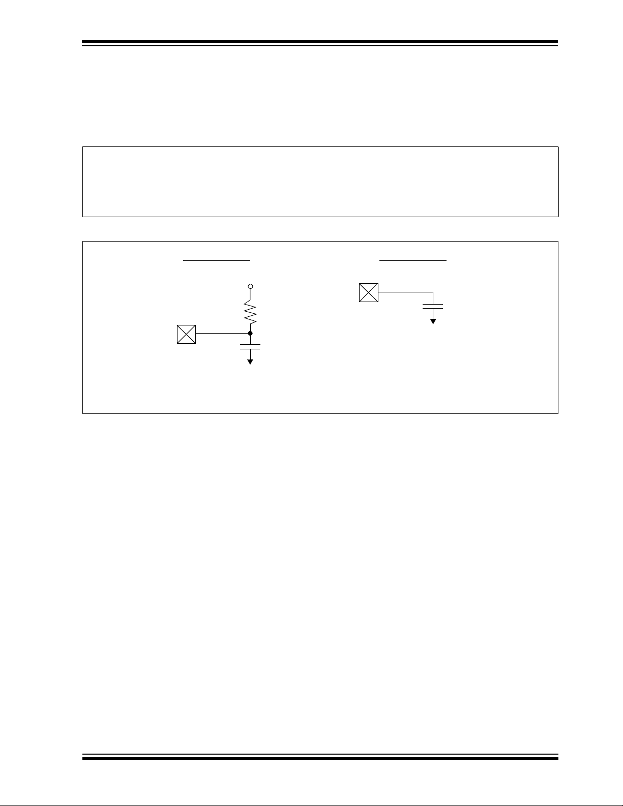
PIC16C62B/72A
VDD/2
C
L
RL
Pin
Pin
VSS
VSS
CL
RL =464
C
L = 50 pF for all pins except OSC2/CLKOUT
15 pF for OSC2 output
Load condition 1
Load condition 2
13.4.2 TIMING CONDITIONS
The temperature and voltages specified in Table 13-1
apply to all timing specifications unless otherwise
noted. Figure 13-4 specifies the load conditions for the
timing specifications.
TABLE 13-1: TEMPERATURE AND VOLTAGE SPECIFICATIONS - AC
AC CHARACTERISTICS Standard Operating Conditions (unless otherwise stated)
Operating temperature 0°C T
-40°C T
-40°C T
Operating voltage V
LC parts operate for commercial/industrial temp’s only.
DD range as described in DC spec Section 13.1 and Section 13.2.
FIGURE 13-4: LOAD CONDITIONS FOR DEVICE TIMING SPECIFICATIONS
A +70°C for commercial
A +85°C for industrial
A +125°C for extended
1998-2013 Microchip Technology Inc. Preliminary DS35008C-page 89
Page 90
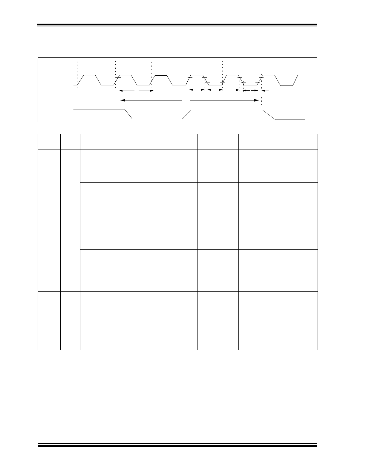
PIC16C62B/72A
3
3
4
4
1
2
Q4
Q1 Q2 Q3 Q4
Q1
OSC1
CLKOUT
13.4.3 TIMING DIAGRAMS AND SPECIFICATIONS
FIGURE 13-5: EXTERNAL CLOCK TIMING
TABLE 13-2: EXTERNAL CLOCK TIMING REQUIREMENTS
Param
No.
1A Fosc External CLKIN Frequency
1
2
3*
4*
Note 1: Instruction cycle period (T
Sym Characteristic Min Typ† Max Units Conditions
DC — 4 MHz RC and XT osc modes
(Note 1)
Oscillator Frequency
(Note 1)
Tosc External CLKIN Period
(Note 1)
Oscillator Period
(Note 1)
TCY Instruction Cycle Time (Note 1) 200 — DC ns TCY = 4/FOSC
To sL ,
To sH
To sR ,
To sF
* These parameters are characterized but not tested.
† Data in "Typ" column is at 5V, 25°C unless otherwise stated. These parameters are for design guidance only
and are not tested.
based on characterization data for that particular oscillator type under standard operating conditions with the
device executing code. Exceeding these specified limits may result in an unstable oscillator operation and/or
higher than expected current consumption. All devices are tested to operate at "min." values with an external
clock applied to the OSC1/CLKIN pin.
When an external clock input is used, the "Max." cycle time limit is "DC" (no clock) for all devices.
External Clock in (OSC1) High
or Low Time
External Clock in (OSC1) Rise
or Fall Time
CY) equals four times the input oscillator time-base period. All specified values are
DC — 4 MHz HS osc mode (-04)
DC — 20 MHz HS osc mode (-20)
DC — 200 kHz LP osc mode
DC — 4 MHz RC osc mode
0.1 — 4 MHz XT osc mode
4 — 20 MHz HS osc mode
5 — 200 kHz LP osc mode
250 — — ns RC and XT osc modes
250 — — ns HS osc mode (-04)
50 — — ns HS osc mode (-20)
5— —sLP osc mode
250 — — ns RC osc mode
250 — 10,000 ns XT osc mode
250 — 250 ns HS osc mode (-04)
50 — 250 ns HS osc mode (-20)
5— —sLP osc mode
100 — — ns XT oscillator
2.5 — — s LP oscillator
15 — — ns HS oscillator
— — 25 ns XT oscillator
— — 50 ns LP oscillator
— — 15 ns HS oscillator
DS35008C-page 90 Preliminary 1998-2013 Microchip Technology Inc.
Page 91
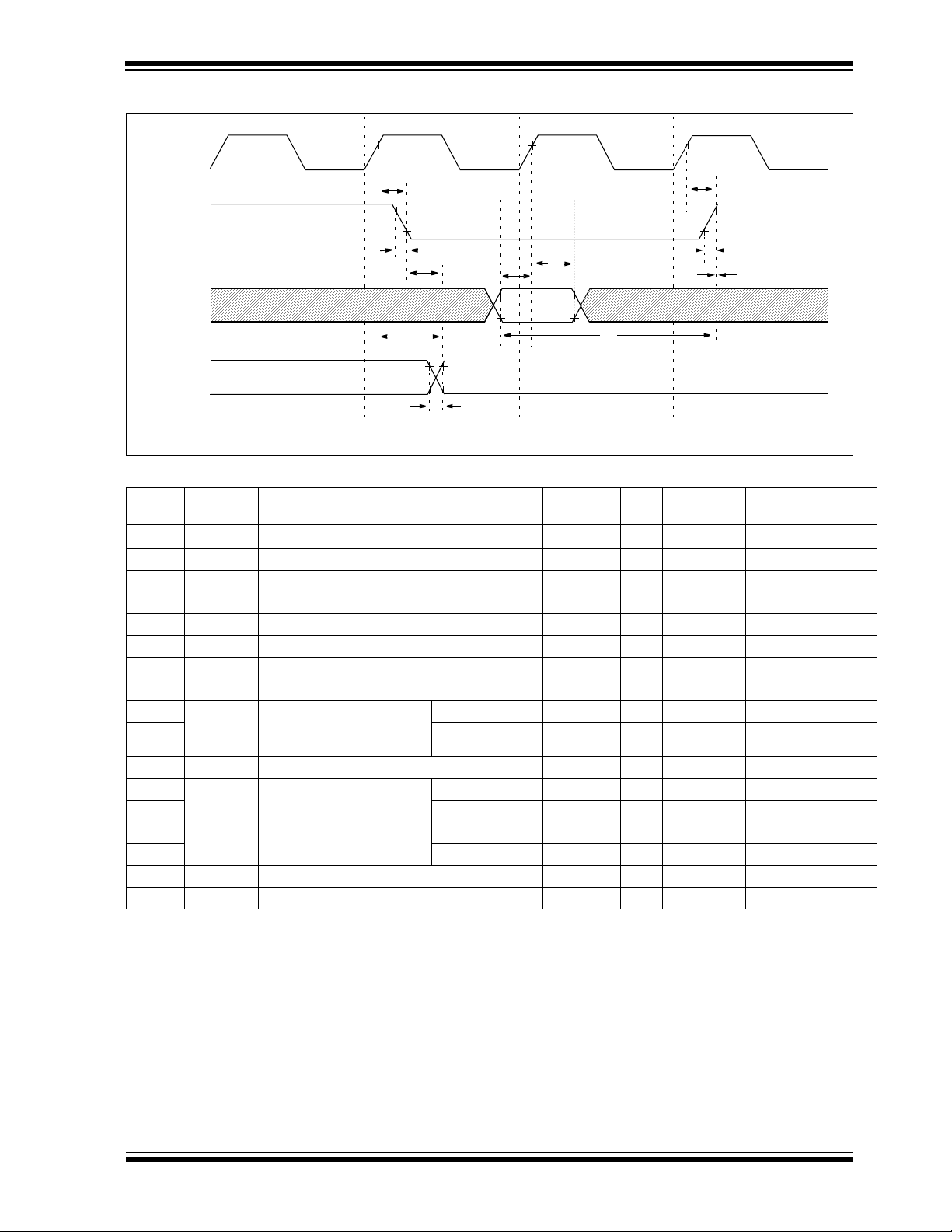
Note: Refer to Figure 13-4 for load conditions.
OSC1
CLKOUT
I/O Pin
(input)
I/O Pin
(output)
Q4
Q1
Q2 Q3
10
13
14
17
20, 21
19
18
15
11
12
16
old value
new value
PIC16C62B/72A
FIGURE 13-6: CLKOUT AND I/O TIMING
TABLE 13-3: CLKOUT AND I/O TIMING REQUIREMENTS
Param
18A*
20A*
21A*
22††*
23††*
Note 1: Measurements are taken in RC Mode where CLKOUT output is 4 x TOSC.
Sym Characteristic Min Typ† Max Units Conditions
No.
10*
TosH2ckL OSC1 to CLKOUT — 75 200 ns Note 1
11*
TosH2ckH OSC1 to CLKOUT — 75 200 ns Note 1
12*
TckR CLKOUT rise time — 35 100 ns Note 1
13*
TckF CLKOUT fall time — 35 100 ns Note 1
14*
TckL2ioV CLKOUT to Port out valid — — 0.5TCY + 20 ns Note 1
15*
TioV2ckH Port in valid before CLKOUT Tosc + 200 — — ns Note 1
16*
TckH2ioI Port in hold after CLKOUT 0——nsNote 1
17*
To s H 2 io V O S C 1 (Q1 cycle) to Port out valid — 50 150 ns
18*
To s H 2 io I O S C 1 (Q2 cycle) to Port
input invalid (I/O in hold
time)
19*
TioV2osH Port input valid to OSC1(I/O in setup time) 0 — — ns
20*
TioR Port output rise time PIC16CXX —10 40 ns
PIC16CXX 100 — — ns
PIC16LCXX 200 — — ns
PIC16LCXX — — 80 ns
21*
TioF Port output fall time PIC16CXX —10 40 ns
PIC16LCXX — — 80 ns
Tinp INT pin high or low time TCY —— ns
Trbp RB7:RB4 change INT high or low time TCY —— ns
* These parameters are characterized but not tested.
† Data in "Typ" column is at 5V, 25°C unless otherwise stated. These parameters are for design guidance only and
are not tested.
††These parameters are asynchronous events not related to any internal clock edge.
1998-2013 Microchip Technology Inc. Preliminary DS35008C-page 91
Page 92

PIC16C62B/72A
VDD
MCLR
Internal
POR
PWRT
Time-out
OSC
Time-out
Internal
RESET
Watchdog
Timer
RESET
33
32
30
31
34
I/O Pins
34
Note: Refer to Figure 13-4 for load conditions.
VDD
BVDD
35
FIGURE 13-7: RESET, WATCHDOG TIMER, OSCILLATOR START-UP TIMER AND POWER-UP
TIMER TIMING
FIGURE 13-8: BROWN-OUT RESET TIMING
TABLE 13-4: RESET, WATCHDOG TIMER, OSCILLATOR START-UP TIMER, POWER-UP TIMER
AND BROWN-OUT RESET REQUIREMENTS
Param
No.
30
31*
32
33*
34
35
Sym Characteristic Min Typ† Max Units Conditions
TmcL MCLR Pulse Width (low) 2 — — sVDD = 5V, -40°C to +125°C
Twdt Watchdog Timer Time-out Period
71833msVDD = 5V, -40°C to +125°C
(No Prescaler)
Tost Oscillator Start-up Timer Period — 1024
Tpwrt Power-up Timer Period 28 72 132 ms VDD = 5V, -40°C to +125°C
TIOZ I/O Hi-impedance from MCLR
Low or WDT reset
T
OSC
——2.1s
——TOSC = OSC1 period
TBOR Brown-out Reset Pulse Width 100 — — sVDD BVDD (D005)
* These parameters are characterized but not tested.
† Data in "Typ" column is at 5V, 25°C unless otherwise stated. These parameters are for design guidance only
and are not tested.
DS35008C-page 92 Preliminary 1998-2013 Microchip Technology Inc.
Page 93
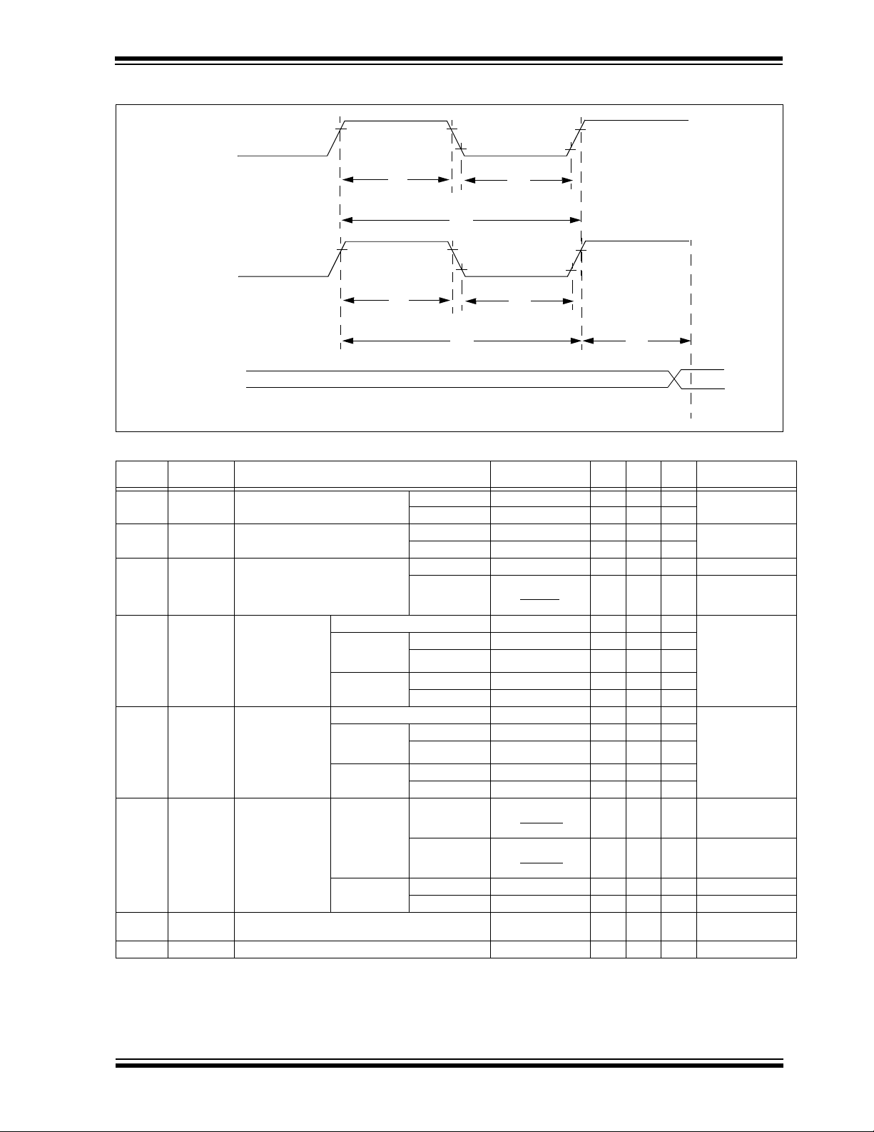
Note: Refer to Figure 13-4 for load conditions.
46
47
45
48
41
42
40
T0CKI
T1OSO/T1CKI
TMR0 or
TMR1
PIC16C62B/72A
FIGURE 13-9: TIMER0 AND TIMER1 EXTERNAL CLOCK TIMINGS
TABLE 13-5: TIMER0 AND TIMER1 EXTERNAL CLOCK REQUIREMENTS
Param
No.
40* Tt0H T0CKI High Pulse Width No Prescaler 0.5T
41* Tt0L T0CKI Low Pulse Width No Prescaler 0.5T
42* Tt0P T0CKI Period No Prescaler T
45* Tt1H T1CKI High Time Synchronous, Prescaler = 1 0.5T
46* Tt1L T1CKI Low Time Synchronous, Prescaler = 1 0.5T
47* Tt1P T1CKI input period Synchronous PIC16CXX G
48 TCKEZtmr1 Delay from external clock edge to timer increment 2Tosc — 7Tosc —
* These parameters are characterized but not tested.
† Data in "Typ" column is at 5V, 25°C unless otherwise stated. These parameters are for design guidance only and are not tested.
Sym Characteristic Min Typ† Max Units Conditions
CY + 20 — — ns Must also meet
With Prescaler 10 — — ns
CY + 20 — — ns Must also meet
With Prescaler 10 — — ns
CY + 40 — — ns
Synchronous,
Prescaler =
2,4,8
Asynchronous PIC16CXX 30 — — ns
Synchronous,
Prescaler =
2,4,8
Asynchronous PIC16CXX 30 — — ns
Ft1 Timer1 oscillator input frequency range
(oscillator enabled by setting bit T1OSCEN)
Asynchronous PIC16CXX 60 — — ns
With Prescaler Greater of:
PIC16CXX 15 — — ns
PIC16LCXX 25 — — ns
PIC16LCXX 50 — — ns
PIC16CXX 15 — — ns
PIC16LCXX 25 — — ns
PIC16LCXX 50 — — ns
PIC16LCXX G
PIC16LCXX 100 — — ns
20 or T
CY + 40
N
CY + 20 — — ns Must also meet
CY + 20 — — ns Must also meet
REATER OF:
30
OR TCY + 40
N
REATER OF:
OR TCY + 40
50
N
DC — 200 kHz
— — ns N = prescale value
— — ns N = prescale value
parameter 42
parameter 42
(2, 4,..., 256)
parameter 47
parameter 47
(1, 2, 4, 8)
N = prescale value
(1, 2, 4, 8)
1998-2013 Microchip Technology Inc. Preliminary DS35008C-page 93
Page 94
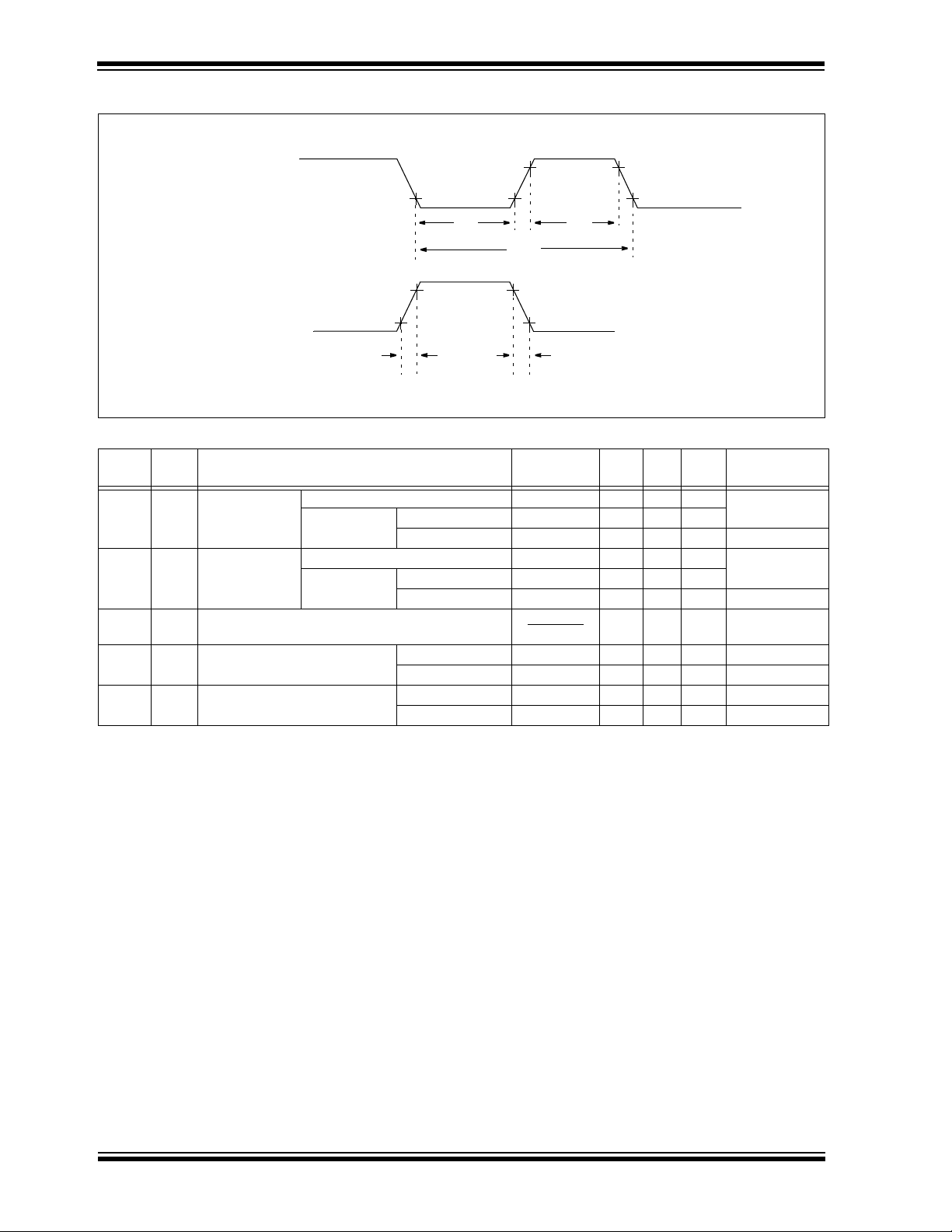
PIC16C62B/72A
Note: Refer to Figure 13-4 for load conditions.
CCP1
(Capture Mode)
50 51
52
CCP1
53
54
(Compare or PWM Mode)
FIGURE 13-10: CAPTURE/COMPARE/PWM TIMINGS
TABLE 13-6: CAPTURE/COMPARE/PWM REQUIREMENTS
Param
No.
50* TccL CCP1 input low
51* TccH CCP1 input high
52* TccP CCP1 input period 3T
53* TccR CCP1 output rise time PIC16CXX —1025ns
54* TccF CCP1 output fall time PIC16CXX —1025ns
Sym Characteristic Min Typ† Max Units Conditions
No Prescaler 0.5TCY + 20 — — ns
time
time
* These parameters are characterized but not tested.
† Data in "Typ" column is at 5V, 25°C unless otherwise stated. These parameters are for design guidance only and are not
tested.
With Prescaler PIC16CXX 10 — — ns
PIC16LCXX 20 — — ns
No Prescaler 0.5T
With Prescaler PIC16CXX 10 — — ns
PIC16LCXX 20 — — ns
PIC16LCXX —2545ns
PIC16LCXX —2545ns
CY + 20 — — ns
CY + 40
N
— — ns N = prescale
value (1,4, or 16)
DS35008C-page 94 Preliminary 1998-2013 Microchip Technology Inc.
Page 95
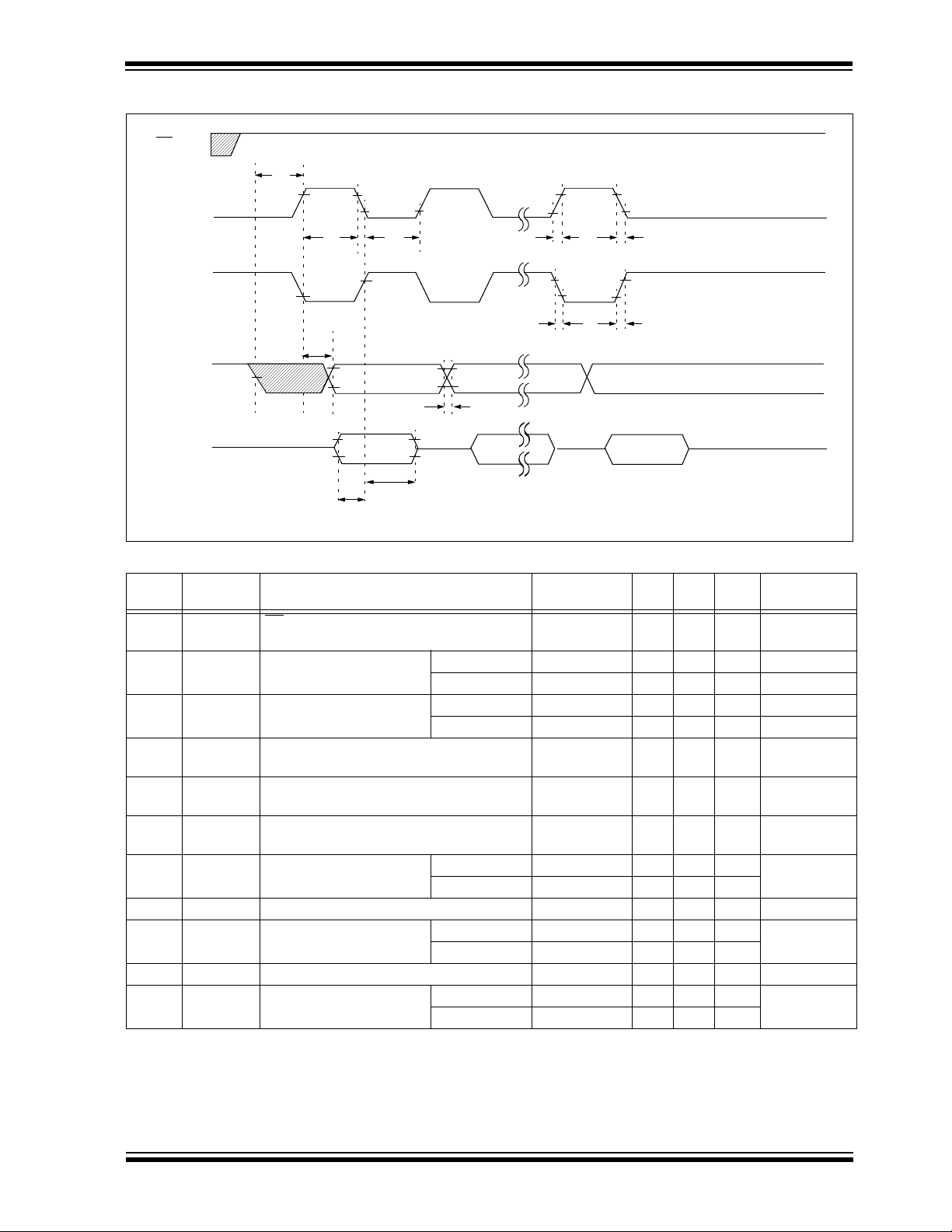
PIC16C62B/72A
SS
SCK
(CKP = 0)
SCK
(CKP = 1)
SDO
SDI
70
71 72
73
74
75, 76
78
79
80
79
78
MSb LSb
BIT6 - - - - - -1
MSb IN
LSb IN
BIT6 - - - -1
Note: Refer to Figure 13-4 for load conditions.
FIGURE 13-11: EXAMPLE SPI MASTER MODE TIMING (CKE = 0)
TABLE 13-7: EXAMPLE SPI MODE REQUIREMENTS (MASTER MODE, CKE = 0)
Param.
Symbol Characteristic Min Typ† Max Units Conditions
No.
70
TssL2scH,
SS to SCK or SCK input TCY —— ns
TssL2scL
71
71A
72
72A
73
TscH SCK input high time
(slave mode)
TscL SCK input low time
(slave mode)
TdiV2scH,
Setup time of SDI data input to SCK edge 100 — — ns
Continuous 1.25TCY + 30 — — ns
Single Byte 40 — — ns Note 1
Continuous 1.25TCY + 30 — — ns
Single Byte 40 — — ns Note 1
TdiV2scL
73A
TB2B Last clock edge of Byte1 to the 1st clock
1.5TCY + 40 — — ns Note 1
edge of Byte2
74
TscH2diL,
Hold time of SDI data input to SCK edge 100 — — ns
TscL2diL
75
76
78
TdoR SDO data output rise time
TdoF SDO data output fall time — 10 25 ns
TscR SCK output rise time
(master mode)
79
80
Note 1: Specification 73A is only required if specifications 71A and 72A are used.
TscF SCK output fall time (master mode) — 10 25 ns
TscH2doV,
TscL2doV
† Data in “Typ” column is at 5V, 25°C unless otherwise stated. These parameters are for design guidance only
and are not tested.
SDO data output valid
after SCK edge
PIC16CXX
PIC16LCXX
PIC16CXX
PIC16LCXX
PIC16CXX
PIC16LCXX
—1025ns
—2045ns
—1025ns
—2045ns
——50ns
— — 100 ns
1998-2013 Microchip Technology Inc. Preliminary DS35008C-page 95
Page 96

PIC16C62B/72A
SS
SCK
(CKP = 0)
SCK
(CKP = 1)
SDO
SDI
81
71 72
74
75, 76
78
80
MSb
79
73
MSb IN
BIT6 - - - - - -1
LSb IN
BIT6 - - - -1
LSb
Note: Refer to Figure 13-4 for load conditions.
FIGURE 13-12: EXAMPLE SPI MASTER MODE TIMING (CKE = 1)
TABLE 13-8: EXAMPLE SPI MODE REQUIREMENTS (MASTER MODE, CKE = 1)
Param.
Symbol Characteristic Min Typ† Max Units Conditions
No.
71
71A
72
72A
73
73A
TscH SCK input high time
(slave mode)
TscL SCK input low time
(slave mode)
TdiV2scH,
TdiV2scL
Setup time of SDI data input to SCK
edge
Continuous 1.25TCY + 30 — — ns
Single Byte 40 — — ns Note 1
Continuous 1.25TCY + 30 — — ns
Single Byte 40 — — ns Note 1
TB2B Last clock edge of Byte1 to the 1st clock
100 — — ns
1.5TCY + 40 — — ns Note 1
edge of Byte2
74
TscH2diL,
Hold time of SDI data input to SCK edge 100 — — ns
TscL2diL
75
TdoR SDO data output rise
time
76
78
TdoF SDO data output fall time — 10 25 ns
TscR SCK output rise time
(master mode)
79
80
81
TscF SCK output fall time (master mode) — 10 25 ns
TscH2doV,
TscL2doV
TdoV2scH,
TdoV2scL
SDO data output valid
after SCK edge
SDO data output setup to SCK edge TCY —— ns
† Data in “Typ” column is at 5V, 25°C unless otherwise stated. These parameters are for design guidance only
PIC16CXX
PIC16LCXX
PIC16CXX
PIC16LCXX
PIC16CXX
PIC16LCXX
—1025ns
20 45 ns
—1025ns
20 45 ns
— — 50 ns
— 100 ns
and are not tested.
Note 1: Specification 73A is only required if specifications 71A and 72A are used.
DS35008C-page 96 Preliminary 1998-2013 Microchip Technology Inc.
Page 97

FIGURE 13-13: EXAMPLE SPI SLAVE MODE TIMING (CKE = 0)
SS
SCK
(CKP = 0)
SCK
(CKP = 1)
SDO
SDI
70
71 72
73
74
75, 76
77
78
79
80
79
78
SDI
MSb LSb
BIT6 - - - - - -1
MSb IN BIT6 - - - -1 LSb IN
83
Note: Refer to Figure 13-4 for load conditions.
PIC16C62B/72A
TABLE 13-9: EXAMPLE SPI MODE REQUIREMENTS (SLAVE MODE TIMING (CKE = 0)
Param.
No.
70
71
71A
72
72A
73
73A
74
75
76
77
78
79
80
83
Note 1: Specification 73A is only required if specifications 71A and 72A are used.
1998-2013 Microchip Technology Inc. Preliminary DS35008C-page 97
Symbol Characteristic Min Typ† Max Units Conditions
TssL2scH,
SS to SCK or SCK input TCY ——ns
TssL2scL
TscH SCK input high time
(slave mode)
TscL SCK input low time
(slave mode)
TdiV2scH,
Setup time of SDI data input to SCK edge 100 — — ns
TdiV2scL
TB2B Last clock edge of Byte1 to the 1st clock
edge of Byte2
TscH2diL,
Hold time of SDI data input to SCK edge 100 — — ns
TscL2diL
TdoR SDO data output rise time
TdoF SDO data output fall time — 10 25 ns
TssH2doZ SS to SDO output hi-impedance 10 — 50 ns
TscR SCK output rise time
(master mode)
TscF SCK output fall time (master mode) — 10 25 ns
TscH2doV,
TscL2doV
TscH2ssH,
TscL2ssH
SDO data output valid
after SCK edge
SS after SCK edge 1.5TCY + 40 — — ns
† Data in “Typ” column is at 5V, 25°C unless otherwise stated. These parameters are for design guidance only
and are not tested.
Continuous 1.25TCY + 30 — — ns
Single Byte 40 — — ns Note 1
Continuous 1.25TCY + 30 — — ns
Single Byte 40 — — ns Note 1
1.5TCY + 40 — — ns Note 1
PIC16CXX
PIC16LCXX
PIC16CXX
PIC16LCXX
PIC16CXX
PIC16LCXX
—1025ns
20 45 ns
—1025ns
20 45 ns
——50ns
— 100 ns
Page 98

PIC16C62B/72A
SS
SCK
(CKP = 0)
SCK
(CKP = 1)
SDO
SDI
70
71 72
82
SDI
74
75, 76
MSb BIT6 - - - - - -1 LSb
77
MSb IN BIT6 - - - -1 LSb IN
80
83
NOTE: Refer to Figure 13-4 for load conditions.
FIGURE 13-14: EXAMPLE SPI SLAVE MODE TIMING (CKE = 1)
TABLE 13-10: EXAMPLE SPI SLAVE MODE REQUIREMENTS (CKE = 1)
Param.
Symbol Characteristic Min Typ† Max Units Conditions
No.
70
TssL2scH,
SS to SCK or SCK input TCY —— ns
TssL2scL
71
71A
72
72A
73A
TscH SCK input high time
(slave mode)
TscL SCK input low time
(slave mode)
Continuous 1.25TCY + 30 — — ns
Single Byte 40 — — ns Note 1
Continuous 1.25TCY + 30 — — ns
Single Byte 40 — — ns Note 1
TB2B Last clock edge of Byte1 to the 1st clock
1.5TCY + 40 — — ns Note 1
edge of Byte2
74
TscH2diL,
Hold time of SDI data input to SCK edge 100 — — ns
TscL2diL
75
76
77
78
79
80
82
83
TdoR SDO data output rise
time
TdoF SDO data output fall time — 10 25 ns
TssH2doZ SS to SDO output hi-impedance 10 — 50 ns
TscR SCK output rise time
(master mode)
TscF SCK output fall time (master mode) — 10 25 ns
TscH2doV,
TscL2doV
SDO data output valid
after SCK edge
TssL2doV SDO data output valid
edge
TscH2ssH,
after SS
SS after SCK edge 1.5TCY + 40 — — ns
PIC16CXX
PIC16LCXX
PIC16CXX
PIC16LCXX
PIC16CXX
PIC16LCXX
PIC16CXX
PIC16LCXX
—1025ns
20 45 ns
—1025ns
—2045ns
——50ns
——100ns
——50ns
——100ns
TscL2ssH
† Data in “Typ” column is at 5V, 25°C unless otherwise stated. These parameters are for design guidance only
and are not tested.
Note 1: Specification 73A is only required if specifications 71A and 72A are used.
DS35008C-page 98 Preliminary 1998-2013 Microchip Technology Inc.
Page 99

FIGURE 13-15: I2C BUS START/STOP BITS TIMING
Note: Refer to Figure 13-4 for load conditions.
91
92
93
SCL
SDA
START
Condition
STOP
Condition
90
2
TABLE 13-11: I
Parameter
No.
90*
91*
92*
93
* These parameters are characterized but not tested.
C BUS START/STOP BITS REQUIREMENTS
Sym Characteristic Min TypMax Unit
TSU:STA START condition 100 kHz mode 4700 — — ns Only relevant for repeated
Setup time 400 kHz mode 600 — —
THD:STA START condition 100 kHz mode 4000 — — ns After this period the first clock
Hold time 400 kHz mode 600 — —
TSU:STO STOP condition 100 kHz mode 4700 — — ns
Setup time 400 kHz mode 600 — —
THD:STO STOP condition 100 kHz mode 4000 — — ns
Hold time 400 kHz mode 600 — —
PIC16C62B/72A
Conditions
s
START condition
pulse is generated
1998-2013 Microchip Technology Inc. Preliminary DS35008C-page 99
Page 100
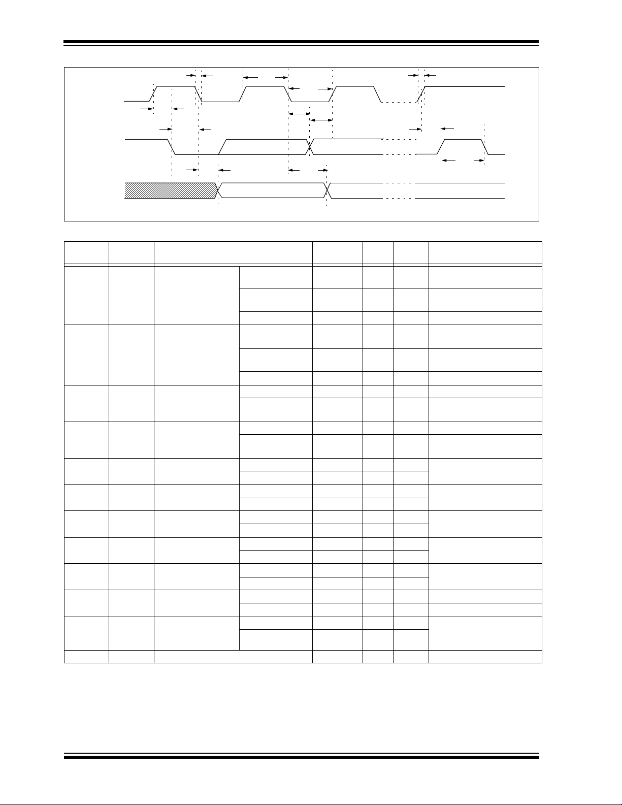
PIC16C62B/72A
Note: Refer to Figure 13-4 for load conditions.
90
91 92
100
101
103
106
107
109
109
110
102
SCL
SDA
In
SDA
Out
FIGURE 13-16: I2C BUS DATA TIMING
TABLE 13-12: I
Param.
2
C BUS DATA REQUIREMENTS
Sym Characteristic Min Max Units Conditions
No.
100* T
HIGH Clock high time 100 kHz mode 4.0 — s Device must operate at a min-
imum of 1.5 MHz
400 kHz mode 0.6 — s Device must operate at a min-
imum of 10 MHz
CY —
101* T
SSP Module 1.5T
LOW Clock low time 100 kHz mode 4.7 — s Device must operate at a min-
imum of 1.5 MHz
400 kHz mode 1.3 — s Device must operate at a min-
imum of 10 MHz
CY —
102* T
R SDA and SCL rise
time
SSP Module 1.5T
100 kHz mode — 1000 ns
400 kHz mode 20 + 0.1Cb 300 ns Cb is specified to be from
10-400 pF
103* T
F SDA and SCL fall
time
100 kHz mode — 300 ns
400 kHz mode 20 + 0.1Cb 300 ns Cb is specified to be from
10-400 pF
90* T
91* T
106* T
SU:STA START condition
setup time
HD:STA START condition hold
time
HD:DAT Data input hold time 100 kHz mode 0 — ns
100 kHz mode 4.7 — s Only relevant for repeated
400 kHz mode 0.6 — s
START condition
100 kHz mode 4.0 — s After this period the first clock
400 kHz mode 0.6 — s
pulse is generated
400 kHz mode 0 0.9 s
107* T
SU:DAT Data input setup time 100 kHz mode 250 — ns Note 2
400 kHz mode 100 — ns
92* T
SU:STO STOP condition setup
time
109* T
AA Output valid from
clock
110* T
* These parameters are characterized but not tested.
Note 1: As a transmitter, the device must provide this internal minimum delay time to bridge the undefined region (min. 300 ns) of the fall-
BUF Bus free time 100 kHz mode 4.7 — s Time the bus must be free
Cb Bus capacitive loading — 400 pF
ing edge of SCL to avoid unintended generation of START or STOP conditions.
2: A fast-mode (400 kHz) I
250 ns must then be met. This will automatically be the case if the device does not stretch the LOW period of the SCL signal. If
such a device does stretch the LOW period of the SCL signal, it must output the next data bit to the SDA line T
max.+tsu;DAT = 1000 + 250 = 1250 ns (according to the standard-mode I
2
C-bus device can be used in a standard-mode (100 kHz) I2C-bus system, but the requirement Tsu:DAT
100 kHz mode 4.7 — s
400 kHz mode 0.6 — s
100 kHz mode — 3500 ns Note 1
400 kHz mode — — ns
400 kHz mode 1.3 — s
2
C bus specification) before the SCL line is released.
before a new transmission
can start
R
DS35008C-page 100 Preliminary 1998-2013 Microchip Technology Inc.
 Loading...