

Page 1

PIC10(L)F320/322
Data Sheet
6/8-Pin, High-Performance,
Flash Microcontrollers
2011 Microchip Technology Inc. Preliminary DS41585A
Page 2

Note the following details of the code protection feature on Microchip devices:
• Microchip products meet the specification contained in their particular Microchip Data Sheet.
• Microchip believes that its family of products is one of the most secure families of its kind on the market today, when used in the
intended manner and under normal conditions.
• There are dishonest and possibly illegal methods used to breach the code protection feature. All of these methods, to our
knowledge, require using the Microchip products in a manner outside the operating specifications contained in Microchip’s Data
Sheets. Most likely, the person doing so is engaged in theft of intellectual property.
• Microchip is willing to work with the customer who is concerned about the integrity of their code.
• Neither Microchip nor any other semiconductor manufacturer can guarantee the security of their code. Code protection does not
mean that we are guaranteeing the product as “unbreakable.”
Code protection is constantly evolving. We at Microchip are committed to continuously improving the code protection features of our
products. Attempts to break Microchip’s code protection feature may be a violation of the Digital Millennium Copyright Act. If such acts
allow unauthorized access to your software or other copyrighted work, you may have a right to sue for relief under that Act.
Information contained in this publication regarding device
applications and the like is provided only for your convenience
and may be superseded by updates. It is your responsibility to
ensure that your application meets with your specifications.
MICROCHIP MAKES NO REPRESENTATIONS OR
WARRANTIES OF ANY KIND WHETHER EXPRESS OR
IMPLIED, WRITTEN OR ORAL, STATUTORY OR
OTHERWISE, RELATED TO THE INFORMATION,
INCLUDING BUT NOT LIMITED TO ITS CONDITION,
QUALITY, PERFORMANCE, MERCHANTABILITY OR
FITNESS FOR PURPOSE. Microchip disclaims all liability
arising from this information and its use. Use of Microchip
devices in life support and/or safety applications is entirely at
the buyer’s risk, and the buyer agrees to defend, indemnify and
hold harmless Microchip from any and all damages, claims,
suits, or expenses resulting from such use. No licenses are
conveyed, implicitly or otherwise, under any Microchip
intellectual property rights.
Trademarks
The Microchip name and logo, the Microchip logo, dsPIC,
K
EELOQ, KEELOQ logo, MPLAB, PIC, PICmicro, PICSTART,
32
PIC
logo, rfPIC and UNI/O are registered trademarks of
Microchip Technology Incorporated in the U.S.A. and other
countries.
FilterLab, Hampshire, HI-TECH C, Linear Active Thermistor,
MXDEV, MXLAB, SEEVAL and The Embedded Control
Solutions Company are registered trademarks of Microchip
Technology Incorporated in the U.S.A.
Analog-for-the-Digital Age, Application Maestro, chipKIT,
chipKIT logo, CodeGuard, dsPICDEM, dsPICDEM.net,
dsPICworks, dsSPEAK, ECAN, ECONOMONITOR,
FanSense, HI-TIDE, In-Circuit Serial Programming, ICSP,
Mindi, MiWi, MPASM, MPLAB Certified logo, MPLIB,
MPLINK, mTouch, Omniscient Code Generation, PICC,
PICC-18, PICDEM, PICDEM.net, PICkit, PICtail, REAL ICE,
rfLAB, Select Mode, Total Endurance, TSHARC,
UniWinDriver, WiperLock and ZENA are trademarks of
Microchip Technology Incorporated in the U.S.A. and other
countries.
SQTP is a service mark of Microchip Technology Incorporated
in the U.S.A.
All other trademarks mentioned herein are property of their
respective companies.
© 2011, Microchip Technology Incorporated, Printed in the
U.S.A., All Rights Reserved.
Printed on recycled paper.
ISBN: 978-1-61341-380-7
Microchip received ISO/TS-16949:2002 certification for its worldwide
headquarters, design and wafer fabrication facilities in Chandler and
Tempe, Arizona; Gresham, Oregon and design centers in California
and India. The Company’s quality system processes and procedures
are for its PIC
devices, Serial EEPROMs, microperipherals, nonvolatile memory and
analog products. In addition, Microchip’s quality system for the design
and manufacture of development systems is ISO 9001:2000 certified.
®
MCUs and dsPIC® DSCs, KEELOQ
®
code hopping
DS41585A-page 2 Preliminary 2011 Microchip Technology Inc.
Page 3

PIC10(L)F320/322
6/8-Pin Flash-Based, 8-Bit Microcontrollers
High-Performance RISC CPU:
• Only 35 Instructions to Learn:
- All single-cycle instructions, except branches
• Operating Speed:
- DC – 16 MHz clock input
- DC – 250 ns instruction cycle
• Up to 512 Words of Flash Program Memory
• 64 Bytes Data Memory
• Eight-level Deep Hardware Stack
• Interrupt Capability
• Processor Self-Write/Read access to Program
Memory
• Pinout Compatible to other 6-Pin PIC10FXXX
Microcontrollers
Special Microcontroller Features:
• Low-Power 16 MHz Internal Oscillator:
- Software selectable frequency range from
16 MHz to 31 kHz
- Factory calibrated to 1%, typical
• Wide Operating Range:
- 1.8V to 3.6V (PIC10LF320/322)
- 2.3V to 5.5V (PIC10F320/322)
• Power-on Reset (POR)
• Power-up Timer (PWRT)
• Brown-out Reset (BOR)
• Ultra Low-Power Sleep Regulator
• Extended Watchdog Timer (WDT)
• Programmable Code Protection
• Power-Saving Sleep mode
• Selectable Oscillator options (EC mode or Internal
Oscillator)
• In-Circuit Serial Programming™ (ICSP™) (via
Two Pins)
• In-Circuit Debugger Support
• Fixed Voltage Reference (FVR) with 1.024V,
2.048V and 4.096V (‘F’ variant only) Output
Levels
• Integrated Temperature Indicator
• 40-year Flash Data Retention
Low-Power Features (PIC10LF320/322):
• Standby Current:
- 20 nA @ 1.8V, typical
• Operating Current:
-25A @ 1 MHz, 1.8V, typical
• Watchdog Timer Current:
- 500 nA @ 1.8V, typical
Peripheral Features:
• 4 I/O Pins:
- 1 input-only pin
- High current sink/source for LED drivers
- Individually selectable weak pull-ups
- Interrupt-on-Change
• Timer0: 8-Bit Timer/Counter with 8-Bit
Programmable Prescaler
• Timer2: 8-Bit Timer/Counter with 8-Bit Period
Register, Prescaler and Postscaler
• Two PWM modules:
- 10-bit PWM, max. frequency 16 kHz
- Combined to single 2-phase output
• A/D Converter:
- 8-bit resolution with 3 channels
• Configurable Logic Cell (CLC):
- 8 selectable input source signals
- Two inputs per module
- Software selectable logic functions including:
AND/OR/XOR/D Flop/D Latch/SR/JK
- External or internal inputs/outputs
- Operation while in Sleep
• Numerically Controlled Oscillator (NCO):
- 20-bit accumulator
- 16-bit increment
- Linear frequency control
- High-speed clock input
- Selectable Output modes
- Fixed Duty Cycle (FDC)
- Pulse Frequency (PF) mode
• Complementary Waveform Generator (CWG):
- Selectable falling and rising edge dead-band
control
- Polarity control
- 2 auto-shutdown sources
- Multiple input sources: PWM, CLC, NCO
2011 Microchip Technology Inc. Preliminary DS41585A-page 3
Page 4
PIC10(L)F320/322
1
2
3
4
5
6
PIC10(L)F320
PIC10(L)F322
RA3/MCLR/V
PP
VDD
RA2
ICSPCLK/RA1
ICSPDAT/RA0
V
SS
SOT-23
1
2
3
4
5
6
7
8
PIC10(L)F320
PIC10(L)F322
RA3/MCLR/V
PP
VSS
N/C
RA0/ICSPDAT
ICSPCLK/RA1
N/C
V
DD
RA2
PDIP, DFN
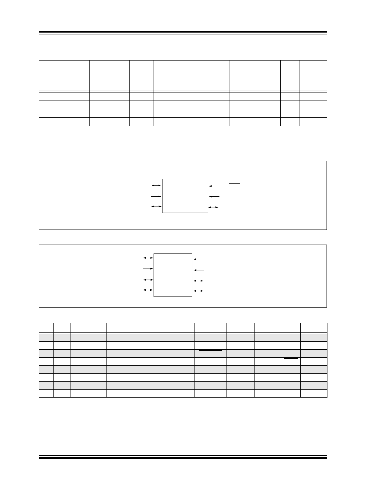
TABLE 1: PIC10(L)F320/322 FEATURE SUMMARY
Program
Device
Memory
Flash
(words)
PIC10F320 256 64 4 3 1 2 2 1 1
PIC10LF320 256 64 4 3 1 2 2 1 1
PIC10F322 512 64 4 3 1 2 2 1 1
PIC10LF322 512 64 4 3 1 2 2 1 1
Note1: One pin is input-only.
FIGURE 1: 6-PIN DIAGRAM, PIC10(L)F320/322
SRAM
(bytes)
I/O
(1)
8-bit A/D (ch) CLC
10-bit
PWM
Timers
8-bit
NCO CWG
FIGURE 2: 8-PIN DIAGRAM, PIC10(L)F320/322
TABLE 2: 6 AND 8-PIN ALLOCATION TABLE (PIC10(L)F320/322)
I/O 6-Pin 8-Pin Analog Timer PWM Interrupts Pull-ups CWG NCO CLC Basic ICSP
RA0 1 5 AN0 — PWM1 IOC0 Y CWG1A — CLC1IN1 — ICSPDAT
RA1 3 4 AN1 — PWM2 IOC1 Y CWG1B NCO1CLK CLC1 CLKIN ICSPCLK
RA2 4 3 AN2 T0CKI — INT/IOC2 Y CWG1FLT NCO1 CLC1IN2 CLKR
RA3 6 8 — — — IOC3 Y — — — MCLR VPP
N/C — 1 — — — — — — — — — —
N/C — 6 — — — — — — — — — —
VDD 5 2 — — — — — — — — VDD —
SS 27 — —— — — — — — VSS —
V
DS41585A-page 4 Preliminary 2011 Microchip Technology Inc.
Page 5

PIC10(L)F320/322
Table of Contents
1.0 Device Overview .......................................................................................................................................................................... 7
2.0 Memory Organization ................................................................................................................................................................. 11
3.0 Device Configuration.................................................................................................................................................................. 21
4.0 Oscillator Module........................................................................................................................................................................ 27
5.0 Resets ........................................................................................................................................................................................ 33
6.0 Interrupts .................................................................................................................................................................................... 41
7.0 Power-Down Mode (Sleep) ........................................................................................................................................................ 51
8.0 Watchdog Timer (WDT) ............................................................................................................................................................. 53
9.0 Flash Program Memory Control ................................................................................................................................................. 57
10.0 I/O Port....................................................................................................................................................................................... 75
11.0 Interrupt-On-Change .................................................................................................................................................................. 81
12.0 Fixed Voltage Reference (FVR) ................................................................................................................................................. 85
13.0 Internal Voltage Regulator (IVR) ................................................................................................................................................ 87
14.0 Temperature Indicator Module ................................................................................................................................................... 89
15.0 Analog-to-Digital Converter (ADC) Module ................................................................................................................................ 91
16.0 Timer0 Module ......................................................................................................................................................................... 101
17.0 Timer2 Module ......................................................................................................................................................................... 105
18.0 Pulse Width Modulation (PWM) Module................................................................................................................................... 107
19.0 Configurable Cell Logic (CLC).................................................................................................................................................. 113
20.0 Numerically Controlled Oscillator (NCO) Module ..................................................................................................................... 129
21.0 Complementary Waveform Generator (CWG) Module ............................................................................................................ 139
22.0 In-Circuit Serial Programming™ (ICSP™) ............................................................................................................................... 155
23.0 Instruction Set Summary.......................................................................................................................................................... 159
24.0 Electrical Specifications............................................................................................................................................................ 169
25.0 DC and AC Characteristics Graphs and Charts ....................................................................................................................... 187
26.0 Development Support............................................................................................................................................................... 189
27.0 Packaging Information.............................................................................................................................................................. 193
Appendix A: Data Sheet Revision History .......................................................................................................................................... 201
Index .................................................................................................................................................................................................. 203
The Microchip Web Site..................................................................................................................................................................... 207
Customer Change Notification Service .............................................................................................................................................. 207
Customer Support .............................................................................................................................................................................. 207
Reader Response .............................................................................................................................................................................. 208
Product Identification System ............................................................................................................................................................ 209
2011 Microchip Technology Inc. Preliminary DS41585A-page 5
Page 6

PIC10(L)F320/322
TO OUR VALUED CUSTOMERS
It is our intention to provide our valued customers with the best documentation possible to ensure successful use of your Microchip
products. To this end, we will continue to improve our publications to better suit your needs. Our publications will be refined and
enhanced as new volumes and updates are introduced.
If you have any questions or comments regarding this publication, please contact the Marketing Communications Department via
E-mail at docerrors@microchip.com or fax the Reader Response Form in the back of this data sheet to (480) 792-4150. We
welcome your feedback.
Most Current Data Sheet
To obtain the most up-to-date version of this data sheet, please register at our Worldwide Web site at:
http://www.microchip.com
You can determine the version of a data sheet by examining its literature number found on the bottom outside corner of any page.
The last character of the literature number is the version number, (e.g., DS30000A is version A of document DS30000).
Errata
An errata sheet, describing minor operational differences from the data sheet and recommended workarounds, may exist for current
devices. As device/documentation issues become known to us, we will publish an errata sheet. The errata will specify the revision
of silicon and revision of document to which it applies.
To determine if an errata sheet exists for a particular device, please check with one of the following:
• Microchip’s Worldwide Web site; http://www.microchip.com
• Your local Microchip sales office (see last page)
When contacting a sales office, please specify which device, revision of silicon and data sheet (include literature number) you are
using.
Customer Notification System
Register on our web site at www.microchip.com to receive the most current information on all of our products.
DS41585A-page 6 Preliminary 2011 Microchip Technology Inc.
Page 7

1.0 DEVICE OVERVIEW
The PIC10(L)F320/322 are described within this data
sheet. They are available in 6/8-pin packages. Figure 1-1
shows a block diagram of the PIC10(L)F320/322
devices. Ta b le 1- 2 shows the pinout descriptions.
Reference Tab le 1- 1 for peripherals available per
device.
TABLE 1-1: DEVICE PERIPHERAL
SUMMARY
Peripheral
PIC10(L)F322
PIC10(L)F320
Analog-to-Digital Converter (ADC) ●●
Configurable Logic Cell (CLC) ●●
Complementary Wave Generator (CWG) ●●
Fixed Voltage Reference (FVR) ●●
Numerically Controlled Oscillator (NCO) ●●
Temperature Indicator ●●
PWM Modules
PWM1 ●●
PWM2 ●●
Timers
Timer0 ●●
Timer2 ●●
PIC10(L)F320/322
2011 Microchip Technology Inc. Preliminary DS41585A-page 7
Page 8
PIC10(L)F320/322
PORTA
Note 1: See applicable chapters for more information on peripherals.
CPU
Program
Flash Memory
RAM
Timing
Generation
INTRC
Oscillator
MCLR
Figure 2-1
CLKIN
CLKR
ADC
8-Bit
FVR
Te mp .
Indicator
Timer2Timer0
PWM1
PWM2 NCO
CLC CWG
FIGURE 1-1: PIC10(L)F320/322 BLOCK DIAGRAM
DS41585A-page 8 Preliminary 2011 Microchip Technology Inc.
Page 9

T ABLE 1-2: PIC10(L)F320/322 PINOUT DESCRIPTION
Input
Name Function
Type
Output
Type
PIC10(L)F320/322
Description
RA0/PWM1/CLC1IN1/CWG1A/
AN0/ICSPDAT
RA1/PWM2/CLC1/CWG1B/AN1/
CLKIN/ICSPCLK/NCO1CLK
RA2/INT/T0CKI/NCO1/CLC1IN2/
CLKR/AN2/CWG1FLT
RA3/MCLR
V
DD VDD Power — Positive supply.
SS VSS Power — Ground reference.
V
Legend: AN = Analog input or output CMOS = CMOS compatible input or output
/VPP RA3 TTL — General purpose input.
TTL = CMOS input with TTL levels ST = CMOS input with Schmitt Trigger levels
HV = High Voltage
RA0 TTL CMOS General purpose I/O with IOC and WPU.
PWM1 — CMOS PWM output.
CLC1IN1
CWG1A —
AN0 AN — A/D Channel input.
ICSPDAT ST CMOS ICSP™ Data I/O.
RA1 TTL CMOS General purpose I/O with IOC and WPU.
PWM2 — CMOS PWM output.
CLC1 — CMOS
CWG1B — CMOS
AN1 AN — A/D Channel input.
CLKIN ST — External Clock input (EC mode).
ICSPCLK ST — Serial Programming Clock.
NCO1CLK ST — Numerical Controlled Oscillator external clock input.
RA2 TTL CMOS General purpose I/O with IOC and WPU.
INT ST — External interrupt.
T0CKI ST — Timer0 clock input.
NCO1 — CMOS Numerically Controlled Oscillator output.
CLC1IN2 ST —
CLKR — CMOS Clock Reference output.
AN2 AN — A/D Channel input.
CWG1FLT
MCLR
PP HV — Programming voltage.
V
ST
CMOS CWG primary output.
ST — Complementary Waveform Generator Fault 1 source input.
ST — Master Clear with internal pull-up.
CLC input.
—
CLC output.
CWG complementary output.
CLC input.
2011 Microchip Technology Inc. Preliminary DS41585A-page 9
Page 10

PIC10(L)F320/322
NOTES:
DS41585A-page 10 Preliminary 2011 Microchip Technology Inc.
Page 11

PIC10(L)F320/322
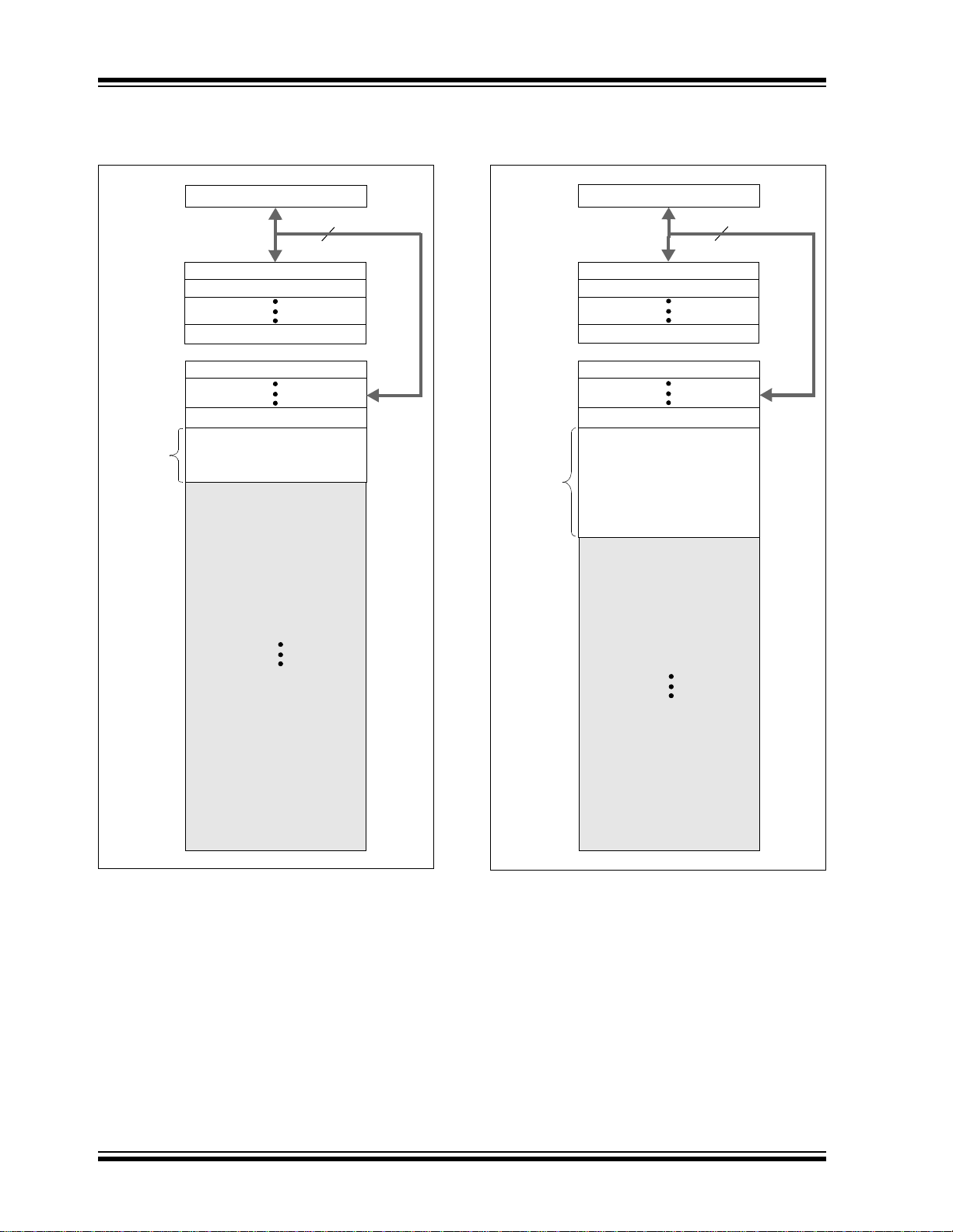
2.0 MEMORY ORGANIZATION
These devices contain the following types of memory:
• Program Memory
- Configuration Words
- Device ID
-User ID
- Flash Program Memory
• Data Memory
- Core Registers
- Special Function Registers
- General Purpose RAM
- Common RAM
The following features are associated with access and
control of program memory and data memory:
• PCL and PCLATH
•Stack
• Indirect Addressing
TABLE 2-1: DEVICE SIZES AND ADDRESSES
Device Program Memory Space (Words) Last Program Memory Address
PIC10(L)F320 256 00FFh
PIC10(L)F322 512 01FFh
2.1 Program Memory Organization
The mid-range core has a 13-bit program counter
capable of addressing 8K x 14 program memory space.
This device family only implements up to 512 words of
the 8K program memory space. Table 2-1 shows the
memory sizes implemented for the PIC10(L)F320/322
family. Accessing a location above these boundaries will
cause a wrap-around within the implemented memory
space. The Reset vector is at 0000h and the interrupt
vector is at 0004h (see Figures 2-1, and 2-2).
2011 Microchip Technology Inc. Preliminary DS41585A-page 11
Page 12
PIC10(L)F320/322
PC<12:0>
13
0000h
0004h
Stack Level 0
Stack Level 8
Reset Vector
Interrupt Vector
Stack Level 1
0005h
On-chip
Program
Memory
Page 0
00FFh
Wraps to Page 0
Wraps to Page 0
Wraps to Page 0
0100h
CALL,
RETURN, RETLW
RETFIE
Rollover to Page 0
Rollover to Page 0
FFFh
PC<12:0>
13
0000h
0004h
Stack Level 0
Stack Level 8
Reset Vector
Interrupt Vector
Stack Level 1
0005h
On-chip
Program
Memory
Page 0
01FFh
Wraps to Page 0
Wraps to Page 0
0200h
CALL
RETURN, RETLW
RETFIE
Rollover to Page 0
Rollover to Page 0
FFFh
FIGURE 2-1: PROGRAM MEMORY MAP
AND STACK FOR
PIC10(L)F320
FIGURE 2-2: PROGRAM MEMORY MAP
AND STACK FOR
PIC10(L)F322
DS41585A-page 12 Preliminary 2011 Microchip Technology Inc.
Page 13

PIC10(L)F320/322
2.2 Data Memory Organization
The data memory is in one bank, which contains the
General Purpose Registers (GPR) and the Special
Function Registers (SFR). The RP<1:0> bits of the
STATUS register are the bank select bits.
RP0
RP1
00 Bank 0 is selected
The bank extends up to 7Fh (128 bytes). The lower
locations of the bank are reserved for the Special Function Registers. Above the Special Function Registers
are the General Purpose Registers, implemented as
Stati c RAM.
2.2.1 GENERAL PURPOSE REGISTER
FILE
The register file is organized as 64 x 8 in the
PIC10(L)F320/322. Each register is accessed, either
directly or indirectly, through the File Select Register
(FSR) (see Section 2.4 “Indirect Addressing, INDF
and FSR Registers”).
2.2.2 SPECIAL FUNCTION REGISTERS
The Special Function Registers are registers used by
the CPU and peripheral functions for controlling the
desired operation of the device (see Tab le 2- 3 ). These
registers are static RAM.
The special registers can be classified into two sets:
core and peripheral. The Special Function Registers
associated with the “core” are described in this section.
Those related to the operation of the peripheral features
are described in the section of that peripheral feature.
2011 Microchip Technology Inc. Preliminary DS41585A-page 13
Page 14

PIC10(L)F320/322
2.2.2.1 STATUS Register
The STATUS register, shown in Register 2-1, contains:
• the arithmetic status of the ALU
• the Reset status
• the bank select bits for data memory (SRAM)
The STATUS register can be the destination for any
instruction, like any other register. If the STATUS
register is the destination for an instruction that affects
the Z, DC or C bits, then the write to these three bits is
disabled. These bits are set or cleared according to the
device logic. Furthermore, the TO
writable. Therefore, the result of an instruction with the
STATUS register as destination may be different than
intended.
For example, CLRF STATUS will clear the upper three
bits and set the Z bit. This leaves the STATUS register
as ‘000u u1uu’ (where u = unchanged).
It is recommended, therefore, that only BCF, BSF,
SWAPF and MOVWF instructions are used to alter the
STATUS register, because these instructions do not
affect any Status bits. For other instructions not affecting any Status bits (see Section 23.0 “Instruction Set
Summary”).
and PD bits are not
Note 1: Bits IRP and RP1 of the STATUS register
are not used by the PIC10(L)F320 and
should be maintained as clear. Use of
these bits is not recommended, since this
may affect upward compatibility with
future products.
2: The C and DC bits operate as a Borrow
and Digit Borrow out bit, respectively, in
subtraction.
DS41585A-page 14 Preliminary 2011 Microchip Technology Inc.
Page 15

PIC10(L)F320/322
REGISTER 2-1: STATUS: STATUS REGISTER
R/W-0/0 R/W-0/0 R/W-0/0 R-1/q R-1/q R/W-x/u R/W-x/u R/W-x/u
IRP RP1 RP0 TO PD ZDCC
bit 7 bit 0
Legend:
R = Readable bit W = Writable bit U = Unimplemented bit, read as ‘0’
u = Bit is unchanged x = Bit is unknown -n/n = Value at POR and BOR/Value at all other Resets
‘1’ = Bit is set ‘0’ = Bit is cleared q = Value depends on condition
bit 7 IRP: Reserved
bit 6-5 RP<1:0>: Reserved
bit 4 TO: Time-out bit
1 = After power-up, CLRWDT instruction or SLEEP instruction
0 = A WDT time-out occurred
bit 3 PD
bit 2 Z: Zero bit
bit 1 DC: Digit Carry/Borrow
bit 0 C: Carry/Borrow bit (ADDWF, ADDLW, SUBLW, SUBWF instructions)
Note1: For Borrow
second operand. For rotate (RRF, RLF) instructions, this bit is loaded with either the high or low-order bit of
the source register.
2: Maintain as ‘0’.
: Power-Down bit
1 = After power-up or by the CLRWDT instruction
0 = By execution of the SLEEP instruction
1 = The result of an arithmetic or logic operation is zero
0 = The result of an arithmetic or logic operation is not zero
1 = A carry-out from the 4th low-order bit of the result occurred
0 = No carry-out from the 4th low-order bit of the result
1 = A carry-out from the Most Significant bit of the result occurred
0 = No carry-out from the Most Significant bit of the result occurred
, the polarity is reversed. A subtraction is executed by adding the two’s complement of the
(2)
(2)
bit (ADDWF, ADDLW, SUBLW, SUBWF instructions)
(1)
(1)
2011 Microchip Technology Inc. Preliminary DS41585A-page 15
Page 16

PIC10(L)F320/322
Legend: = Unimplemented data memory locations, read as ‘0’.
* = Not a physical register.
INDF
(*)
00h
PMADRL
20h
General
Purpose
Registers
32 Bytes
40h
5Fh
General
Purpose
Registers
32 Bytes
60h
7Fh
TMR0 01h PMADRH 21h
PCL 02h PMDATL 22h
STATUS 03h PMDATH 23h
FSR 04h PMCON1 24h
PORTA 05h PMCON2 25h
TRISA 06h CLKRCON 26h
LATA 07h NCO1ACCL 27h
ANSELA
08h
NCO1ACCH
28h
WPUA
09h
NCO1ACCU
29h
PCLATH 0Ah NCO1INCL 2Ah
INTCON 0Bh NCO1INCH 2Bh
PIR1 0Ch Reserved 2Ch
PIE1 0Dh NCO1CON 2Dh
OPTION_REG 0Eh NCO1CLK 2Eh
PCON 0Fh Reserved 2Fh
OSCCON 10h WDTCON 30h
TMR2 11h CLC1CON 31h
PR2 12h CLC1SEL1 32h
T2CON 13h CLC1SEL2 33h
PWM1DCL 14h CLC1POL 34h
PWM1DC 15h CLC1GATE1 35h
PWM1CON 16h CLC1GATE2 36h
PWM2DCL 17h CLC1GATE3 37h
PWM2DC 18h CLC1GATE4 38h
PWM2CON 19h CWG1CON0 39h
IOCAP 1Ah CWG1CON1 3Ah
IOCAN 1Bh CWG1ASD 3Bh
IOCAF 1Ch CWG1RC 3Ch
FVRCON 1Dh CWG1FC 3Dh
ADRES
1Eh
VREGCON
3Eh
ADCON 1Fh
BORCON
3Fh
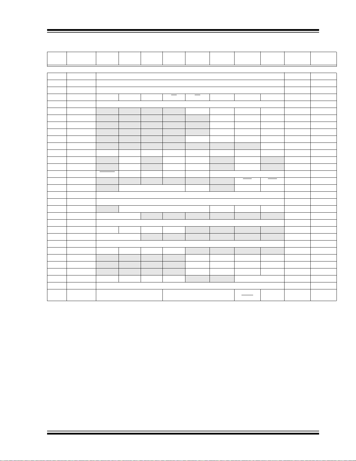
2.2.3 DEVICE MEMORY MAPS
The memory maps for PIC10(L)F320/322 are as shown
in Table 2-2.
TABLE 2-2: PIC10(L)F320/322 MEMORY MAP (BANK 0)
DS41585A-page 16 Preliminary 2011 Microchip Technology Inc.
Page 17
PIC10(L)F320/322
TABLE 2-3: SPECIAL FUNCTION REGISTER SUMMARY (BANK 0)
Address Name Bit 7 Bit 6 Bit 5 Bit 4 Bit 3 Bit 2 Bit 1 Bit 0
Bank 0
00h INDF Addressing this location uses contents of FSR to address data memory (not a physical register) xxxx xxxx xxxx xxxx
01h TMR0 Timer0 Module Register xxxx xxxx uuuu uuuu
02h PCL Program Counter (PC) Least Significant Byte 0000 0000 0000 0000
03h STATUS IRP RP1 RP0 TO
04h FSR Indirect Data Memory Address Pointer xxxx xxxx uuuu uuuu
05h PORTA
06h TRISA
07h LATA
08h ANSELA
09h WPUA
0Ah PCLATH
0Bh INTCON GIE PEIE TMR0IE INTE IOCIE TMR0IF INTF IOCIF 0000 0000 0000 000u
0Ch PIR1
0Dh PIE1
0Eh OPTION_REG WPUEN
0Fh
10h OSCCON
11h TMR2 Timer2 Module Register 0000 0000 0000 0000
12h PR2 Timer2 Period Register 1111 1111 1111 1111
13h T2CON
14h PWM1DCL PWM1DCL<1:0>
15h PWM1DCH PWM1DCH<7:0> xxxx xxxx uuuu uuuu
16h PWM1CON
17h PWM2DCL PWM2DCL<1:0>
18h PWM2DCH PWM2DCH<7:0> xxxx xxxx uuuu uuuu
19h PWM2CON
1Ah IOCAP
1Bh IOCAN
1Ch IOCAF
1Dh FVRCON FVREN FVRRDY TSEN TSRNG
1Eh ADRES A/D Result Register xxxx xxxx uuuu uuuu
1Fh ADCON ADCS<2:0> CHS<2:0>
Legend: x = unknown, u = unchanged, q = value depends on condition, - = unimplemented, read as ‘0’, r = reserved.
Note 1: Unimplemented, read as ‘1’.
PCON — — — — — —PORBOR ---- --qq ---- --uu
Shaded locations are unimplemented, read as ‘0’.
— — — — RA3 RA2 RA1 RA0 ---- xxxx ---- uuuu
— — — — —
— — — — — LATA2 LATA1 LATA0 ---- -xxx ---- -uuu
— — — — — ANSA2 ANSA1 ANSA0 ---- -111 ---- -111
— — — — WPUA3 WPUA2 WPUA1 WPUA0 ---- 1111 ---- 1111
— — — — — — — PCLH0 ---- ---0 ---- ---0
—ADIF— NCO1IF CLC1IF —TMR2IF— -0-0 0-0- -0-0 0-0-
—ADIE— NCO1IE CLC1IE —TMR2IE— -0-0 0-0- -0-0 0-0-
INTEDG T0CS T0SE PSA PS<2:0> 1111 1111 uuuu uuuu
— IRCF<2:0> HFIOFR — LFIOFR HFIOFS -110 0-00 -110 0-00
— TOUTPS<3:0> TMR2ON T2CKPS1 T2CKPS0 -000 0000 -000 0000
— — — — — — xx-- ---- uu-- ----
PWM1EN PWM1OE PWM1OUT PWM1POL — — — —
— — — — — — xx-- ---- uu-- ----
PWM2EN PWM2OE PWM2OUT PWM2POL
— — — — IOCAP3 IOCAP2 IOCAP1 IOCAP0 ---- 0000 ---- 0000
— — — — IOCAN3 IOCAN2 IOCAN1 IOCAN0 ---- 0000 ---- 0000
— — — — IOCAF3 IOCAF2 IOCAF1 IOCAF0 ---- 0000 ---- 0000
PD ZDCC0001 1xxx 000q quuu
(1)
TRISA2 TRISA1 TRISA0 ---- 1111 ---- 1111
— — — — 0000 ---- 0000 ----
— —ADFVR<1:0>0x00 --00 0x00 --00
GO/
DONE
ADON 0000 0000 0000 0000
Value on
POR, BOR
0000 ---- 0000 ----
Value on all
other resets
2011 Microchip Technology Inc. Preliminary DS41585A-page 17
Page 18
PIC10(L)F320/322
TABLE 2-3: SPECIAL FUNCTION REGISTER SUMMARY (BANK 0) (CONTINUED)
Address Name Bit 7 Bit 6 Bit 5 Bit 4 Bit 3 Bit 2 Bit 1 Bit 0
Bank 0 (Continued)
20h PMADRL PMADR<7:0> 0000 0000 0000 0000
21h PMADRH
22h PMDATL PMDAT<7:0> xxxx xxxx uuuu uuuu
23h PMDATH
24h PMCON1
25h PMCON2 Program Memory Control Register 2 (not a physical register) 0000 0000 0000 0000
26h CLKRCON
27h NCO1ACCL NCO1 Accumulator <7:0> 0000 0000 0000 0000
28h NCO1ACCH NCO1 Accumulator <15:8> 0000 0000 0000 0000
29h NCO1ACCU
2Ah NCO1INCL NCO1 Increment <7:0> 0000 0001 0000 0001
2Bh NCO1INCH NCO1 Increment <15:8> 0000 0000 0000 0000
2Ch
2Dh NCO1CON N1EN N1OE N1OUT N1POL
2Eh NCO1CLK
2Fh
30h WDTCON
31h
32h
33h
34h
35h
36h
37h
38h
39h CWG1CON0
3Ah CWG1CON1
3Bh CWG1CON2 G1ASE G1ARSEN
3Ch CWG1DBR
3Dh CWG1DBF
3Eh
3Fh
Legend: x = unknown, u = unchanged, q = value depends on condition, - = unimplemented, read as ‘0’, r = reserved.
Note 1: Unimplemented, read as ‘1’.
— Unimplemented — —
Reserved Reserved xxxx xxxx uuuu uuuu
CLC1CON
CLC1SEL0
CLC1SEL1
CLC1POL
CLC1GLS0
CLC1GLS1
CLC1GLS2
CLC1GLS3
VREGCON
BORCON
Shaded locations are unimplemented, read as ‘0’.
— — — — — — — PMADR8 ---- ---0 ---- ---0
— —PMDAT<13:8>--xx xxxx --uu uuuu
— CFGS LWL O FR EE WRERR WREN WR RD 1000 0000 1000 q000
—CLKROE— — — — — — -0-- ---- -0-- ----
— NCO1 Accumulator <19..16> --- - 00 00 ---- 0000
— — —N1PFM0000 ---0 00x0 ---0
N1PWS<2:0> — — —N1CKS<1:0>
— —WDTPS<4:0>SWDTEN--01 0110 --01 0110
LC1EN LC1OE LC1OUT LC1INTP LC1INTN LC1MODE<2:0> 00x0 -000 00x0 -000
— LC1D2S<2:0> — LC1D1S<2:0> -xxx -xxx -uuu -uuu
— LC1D4S<2:0> — LC1D3S<2:0> -xxx -xxx -uuu -uuu
LC1POL
LC1G1D4T LC1G1D4N LC1G1D3T LC1G1D3N LC1G1D 2T LC1G 1D2N LC1G1D1 T LC1G 1D1N
LC1G2D4T LC1G2D4N LC1G2D3T LC1G2D3N LC1G2D 2T LC1G 2D2N LC1G2D1 T LC1G 2D1N
LC1G3D4T LC1G3D4N LC1G3D3T LC1G3D3N LC1G3D 2T LC1G 3D2N LC1G3D1 T LC1G 3D1N
LC1G4D4T LC1G4D4N LC1G4D3T LC1G4D3N LC1G4D 2T LC1G 4D2N LC1G4D1 T LC1G 4D1N
G1EN G1OEB G1OEA G1POLB G1POLA
G1ASDLB<1:0> G1ASDLA<1:0>
— —CWG1DBR<5:0>--xx xxxx --uu uuuu
— —CWG1DBF<5:0>--xx xxxx --uu uuuu
— — — — — —VREGPM1Reserved ---- --01 ---- --01
SBOREN BORFS — — — — — BORRDY 10-- ---q uu-- ---u
— — — LC1G4POL LC1G3POL LC1G2POL LC1G1POL 0--- xxxx 0--- uuuu
— —
— —
— — — — G1ASDCLC1 G1ASDFLT xx-- --xx uu-- --uu
G1CS0
G1IS<1:0>
Value on
POR, BOR
000- --00 000- --00
xxxx xxxx uuuu uuuu
xxxx xxxx uuuu uuuu
xxxx xxxx uuuu uuuu
xxxx xxxx uuuu uuuu
0000 0--0 0000 0--0
xxxx --xx uuuu --uu
Value on all
other resets
DS41585A-page 18 Preliminary 2011 Microchip Technology Inc.
Page 19
PIC10(L)F320/322
PC
12 8 7 0
5
PCLATH<4:0>
PCLATH
Instruction with
ALU Result
GOTO, CALL
OPCODE <10:0>
8
PC
12 11 10 0
11
PCLATH<4:3>
PCH PCL
87
2
PCLATH
PCH PCL
PCL as
Destination
MOVLW 0x40 ;initialize pointer
MOVWF FSR ;to RAM
NEXT CLRF INDF ;clear INDF register
INCF FSR ;inc pointer
BTFSS FSR,7 ;all done?
GOTO NEXT ;no clear next
CONTINUE ;yes continue
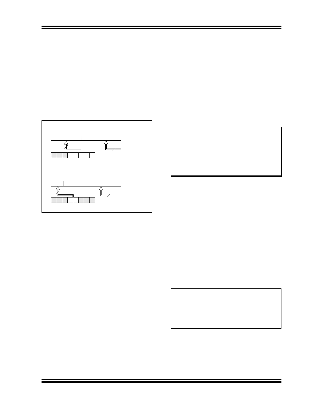
2.3 PCL and PCLATH
The Program Counter (PC) is 13 bits wide. The low byte
comes from the PCL register, which is a readable and
writable register. The high byte (PC<12:8>) is not directly
readable or writable and comes from PCLATH. On any
Reset, the PC is cleared. Figure 2-3 shows the two
situations for the loading of the PC. The upper example
in Figure 2-3 shows how the PC is loaded on a write to
PCL (PCLATH<4:0> PCH). The lower example in
Figure 2-3 shows how the PC is loaded during a CALL or
GOTO instruction (PCLATH<4:3> PCH).
FIGURE 2-3: LOADING OF PC IN
DIFFERENT SITUATIONS
2.3.2 STACK
All devices have an 8-level x 13-bit wide hardware
stack (see Figure 2-1). The stack space is not part of
either program or data space and the Stack Pointer is
not readable or writable. The PC is PUSHed onto the
stack when a CALL instruction is executed or an interrupt causes a branch. The stack is POPed in the event
of a RETURN, RETLW or a RETFIE instruction execution. PCLATH is not affected by a PUSH or POP operation.
The stack operates as a circular buffer. This means that
after the stack has been PUSHed eight times, the ninth
push overwrites the value that was stored from the first
push. The tenth push overwrites the second push (and
so on).
Note 1: There are no Status bits to indicate Stack
Overflow or Stack Underflow conditions.
2: There are no instructions/mnemonics
called PUSH or POP. These are actions
that occur from the execution of the
CALL, RETURN, RETLW and RETFIE
instructions or the vectoring to an
interrupt address.
2.4 Indirect Addressing, INDF and
FSR Registers
2.3.1 MODIFYING PCL
Executing any instruction with the PCL register as the
destination simultaneously causes the Program
Counter PC<12:8> bits (PCH) to be replaced by the
contents of the PCLATH register. This allows the entire
contents of the program counter to be changed by
writing the desired upper 5 bits to the PCLATH register.
When the lower 8 bits are written to the PCL register, all
13 bits of the program counter will change to the values
contained in the PCLATH register and those being
written to the PCL register.
A computed GOTO is accomplished by adding an offset
to the program counter (ADDWF PCL). Care should be
exercised when jumping into a look-up table or
program branch table (computed GOTO) by modifying
the PCL register. Assuming that PCLATH is set to the
table start address, if the table length is greater than
255 instructions or if the lower 8 bits of the memory
address rolls over from 0xFF to 0x00 in the middle of
the table, then PCLATH must be incremented for each
address rollover that occurs between the table
beginning and the target location within the table.
For more information refer to Application Note AN556,
“Implementing a Table Read” (DS00556).
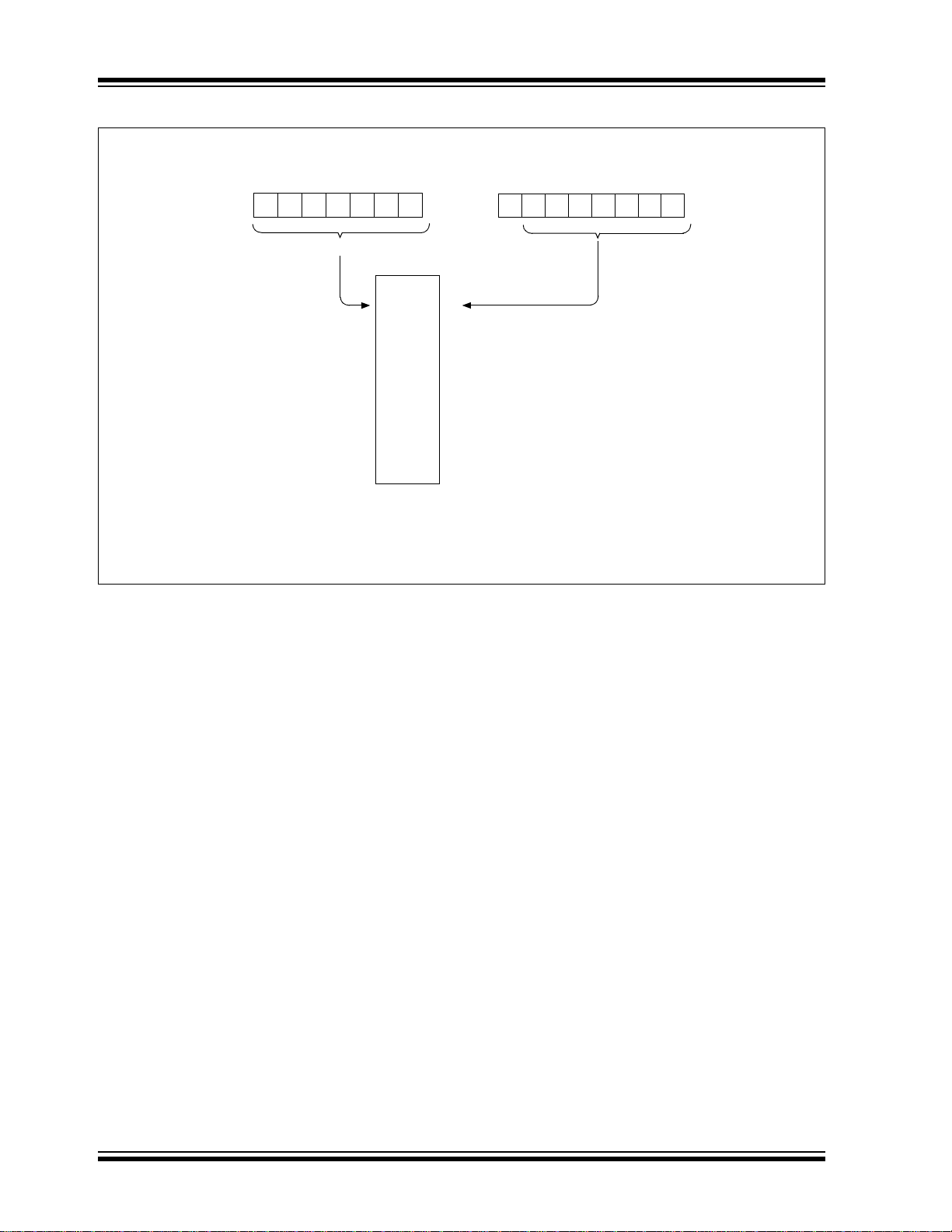
The INDF register is not a physical register. Addressing
the INDF register will cause indirect addressing.
Indirect addressing is possible by using the INDF
register. Any instruction using the INDF register
actually accesses data pointed to by the File Select
Register (FSR). Reading INDF itself indirectly will
produce 00h. Writing to the INDF register indirectly
results in a no operation (although Status bits may be
affected). An effective 9-bit address is obtained by
concatenating the 8-bit FSR and the IRP bit of the
STATUS register, as shown in Figure 2-4.
A simple program to clear RAM location 40h-7Fh using
indirect addressing is shown in Example 2-1.
EXAMPLE 2-1: INDIRECT ADDRESSING
2011 Microchip Technology Inc. Preliminary DS41585A-page 19
Page 20
PIC10(L)F320/322
Data
Memory
Indirect AddressingDirect Addressing
Location Select
6
0
From Opcode
File Select Register
7
0
Location Select
00h
7Fh
Bank 0
For memory map detail, see Figure 2-2.
FIGURE 2-4: DIRECT/INDIRECT ADDRESSING PIC10(L)F320/322
DS41585A-page 20 Preliminary 2011 Microchip Technology Inc.
Page 21

3.0 DEVICE CONFIGURATION
Device Configuration consists of Configuration Word
and Device ID.
3.1 Configuration Word
There are several Configuration Word bits that allow
different oscillator and memory protection options.
These are implemented as Configuration Word at
2007h.
PIC10(L)F320/322
2011 Microchip Technology Inc. Preliminary DS41585A-page 21
Page 22

PIC10(L)F320/322
REGISTER 3-1: CONFIG: CONFIGURATION WORD
U-1 R/P-1/1 R/P-1/1 R/P-1/1 R/P-1/1
— WRT<1:0> BORV LPBOR
bit 13 bit 8
R/P-1/1 R/P-1/1 R/P-1/1 R/P-1/1 R/P-1/1 R/P-1/1 R/P-1/1
CP MCLRE PWRTE WDTE<1:0> BOREN<1:0>
bit 7 bit 0
Legend:
R = Readable bit W = Writable bit U = Unimplemented bit, read as ‘0’
u = Bit is unchanged x = Bit is unknown -n/n = Value at POR and BOR/Value at all other Resets
‘1’ = Bit is set ‘0’ = Bit is cleared P = Programmable bit
bit 13 Unimplemented: Read as ‘1’
bit 12-11 WRT<1:0>: Flash Memory Self-Write Protection bits
256 W Flash memory: PIC10(L)F320:
11 =Write protection off
10 =000h to 03Fh write-protected, 040h to 0FFh may be modified by PMCON control
01 =000h to 07Fh write-protected, 080h to 0FFh may be modified by PMCON control
00 =000h to 0FFh write-protected, no addresses may be modified by PMCON control
512 W Flash memory: PIC10(L)F322:
11 =Write protection off
10 =000h to 07Fh write-protected, 080h to 1FFh may be modified by PMCON control
01 =000h to 0FFh write-protected, 100h to 1FFh may be modified by PMCON control
00 =000h to 1FFh write-protected, no addresses may be modified by PMCON control
bit 10 BORV: Brown-out Reset Voltage Selection bit
1 = Brown-out Reset Voltage (V
0 = Brown-out Reset Voltage (V
bit 9 LPBOR: Low-Power Brown-out Reset Enable bit
1 = Low-power Brown-out Reset is enabled
0 = Low-power Brown-out Reset is disabled
bit 8 LVP: Low-Voltage Programming Enable bit
1 = Low-Voltage Programming enabled. MCLR
0 = High Voltage on MCLR
bit 7 CP
bit 6 MCLRE: MCLR
bit 5 PWRTE
: Code Protection bit
1 = Program memory code protection is disabled
0 = Program memory code protection is enabled
If LVP bit =
This bit is ignored.
If LVP bit = 0:
1 =MCLR
0 =MCLR
1 = PWRT disabled
0 = PWRT enabled
1:
/VPP pin function is MCLR; Weak pull-up enabled.
/VPP pin function is digital input; MCLR internally disabled; Weak pull-up under control of
WPUA3 bit.
: Power-up Timer Enable bit
/VPP Pin Function Select bit
(2)
BOR) set to 1.9V (PIC10LF320/322) or 2.4V (PIC10F320/322)
BOR) set to 2.7V
/VPP pin function is MCLR.
/VPP must be used for programming
(1)
R/P-1/1
LVP
R/P-1/1
FOSC
Note 1: Enabling Brown-out Reset does not automatically enable Power-up Timer.
2: Once enabled, code-protect can only be disabled by bulk erasing the device.
DS41585A-page 22 Preliminary 2011 Microchip Technology Inc.
Page 23

PIC10(L)F320/322
REGISTER 3-1: CONFIG: CONFIGURATION WORD (CONTINUED)
bit 4-3 WDTE<1:0>: Watchdog Timer Enable bit
11 = WDT enabled
10 = WDT enabled while running and disabled in Sleep
01 = WDT controlled by the SWDTEN bit in the WDTCON register
00 = WDT disabled
bit 2-1 BOREN<1:0>: Brown-out Reset Enable bits
11 = Brown-out Reset enabled; SBOREN bit is ignored
10 = Brown-out Reset enabled while running, disabled in Sleep; SBOREN bit is ignored
01 = Brown-out Reset controlled by the SBOREN bit in the BORCON register
00 = Brown-out Reset disabled; SBOREN bit is ignored
bit 0 FOSC: Oscillator Selection bit
1 = EC on CLKIN pin
0 = INTOSC oscillator I/O function available on CLKIN pin
Note 1: Enabling Brown-out Reset does not automatically enable Power-up Timer.
2: Once enabled, code-protect can only be disabled by bulk erasing the device.
2011 Microchip Technology Inc. Preliminary DS41585A-page 23
Page 24

PIC10(L)F320/322
3.2 Code Protection
Code protection allows the device to be protected from
unauthorized access. Program memory protection and
data memory protection are controlled independently.
Internal access to the program memory and data
memory are unaffected by any code protection setting.
3.2.1 PROGRAM MEMORY PROTECTION
The entire program memory space is protected from
external reads and writes by the CP
Word. When CP
program memory are inhibited and a read will return all
‘0’s. The CPU can continue to read program memory,
regardless of the protection bit settings. Writing the
program memory is dependent upon the write
protection setting. See Section 3.3 “Write
Protection” for more information.
= 0, external reads and writes of
3.3 Write Protecti on
Write protection allows the device to be protected from
unintended self-writes. Applications, such as boot
loader software, can be protected while allowing other
regions of the program memory to be modified.
The WRT<1:0> bits in Configuration Word define the
size of the program memory block that is protected.
bit in Configuration
3.4 User ID
Four memory locations (2000h-2003h) are designated
as ID locations where the user can store checksum or
other code identification numbers. These locations are
readable and writable during normal execution. See
Section 3.5 “Device ID and Revision ID” for more
information on accessing these memory locations.
more information on checksum calculation, see the
“PIC10(L)F320/322 Flash Memory Programming
Specification” (DS41572).
For
DS41585A-page 24 Preliminary 2011 Microchip Technology Inc.
Page 25

PIC10(L)F320/322
Device
DEVICEID<13:0> Values
DEV<8:0> REV<4:0>
PIC10F320 10 1001 101 x xxxx
PIC10LF320 10 1001 111 x xxxx
PIC10F322 10 1001 100 x xxxx
PIC10LF322 10 1001 110 x xxxx
3.5 Device ID and Revision ID
The memory location 2006h is where the Device ID and
Revision ID are stored. The upper nine bits hold the
Device ID. The lower five bits hold the Revision ID. See
Section 9.4 “User ID, Device ID and Configuration
Word Access” for more information on accessing
these memory locations.
Development tools, such as device programmers and
debuggers, may be used to read the Device ID and
Revision ID.
REGISTER 3-2: DEVICEID: DEVICE ID REGISTER
RRRRRR
DEV8 DEV7 DEV6 DEV5 DEV4 DEV3
bit 13 bit 8
RRRRRRRR
DEV2 DEV1 DEV0 REV4 REV3 REV2 REV1 REV0
bit 7 bit 0
(1)
Legend: U = Unimplemented bit, read as ‘0’
R = Readable bit W = Writable bit ‘0’ = Bit is cleared
-n = Value at POR ‘1’ = Bit is set x = Bit is unknown
bit 13-5 DEV<8:0>: Device ID bits
bit 4-0 REV<4:0>: Revision ID bits
These bits are used to identify the revision.
Note 1: This location cannot be written.
2011 Microchip Technology Inc. Preliminary DS41585A-page 25
Page 26

PIC10(L)F320/322
NOTES:
DS41585A-page 26 Preliminary 2011 Microchip Technology Inc.
Page 27
PIC10(L)F320/322
HFINTOSC
16 MHz
HFIOFR
(1)
HFIOFS
(1)
Divider
16 MHz
8 MHz
4 MHz
2 MHz
1 MHz
500 kHz
250 kHz
MUX
111
110
101
100
011
010
001
LFINTOSC
31 kHz
000
IRCF<2:0>
INTOSC
LFIOFR
(1)
CLKIN
EC
MUX
FOSC
(Configuration
Word)
System Clock
(CPU and
Peripherals)
CLKROE
CLKR
31 kHz
0
1
3
Note 1: HFIOFR, HFIOFS and LFIOFR are Status bits in the OSCCON register.
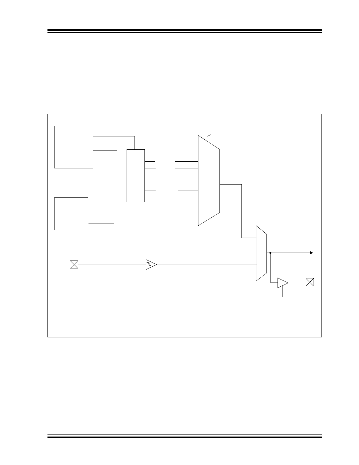
4.0 OSCILLATOR MODULE
4.1 Overview
The oscillator module has a variety of clock sources and
selection features that allow it to be used in a range of
applications while maximizing performance and
minimizing power consumption. Figure 4-1 illustrates a
block diagram of the oscillator module.
The system can be configured to use an internal
calibrated high-frequency oscillator as clock source, with
a choice of selectable speeds via software.
Clock source modes are configured by the FOSC bit in
Configuration Word (CONFIG).
1. EC oscillator from CLKIN.
2. INTOSC oscillator, CLKIN not enabled.
FIGURE 4-1: PIC10(L)F320/322 CLOCK SOURCE BLOCK DIAGRAM
2011 Microchip Technology Inc. Preliminary DS41585A-page 27
Page 28

PIC10(L)F320/322
4.2 Clock Source Modes
Clock source modes can be classified as external or
internal.
• Internal clock source (INTOSC) is contained
within the oscillator module, which has eight
selectable output frequencies, with a maximum
internal frequency of 16 MHz.
• The External Clock mode (EC) relies on an
external signal for the clock source.
The system clock can be selected between external or
internal clock sources via the FOSC bit of the
Configuration Word.
4.3 Internal Clock Modes
The internal clock sources are contained within the
oscillator module. The internal oscillator block has two
internal oscillators that are used to generate all internal
system clock sources: the 16 MHz High-Frequency
Internal Oscillator (HFINTOSC) and the 31 kHz
(LFINTOSC).
The HFINTOSC consists of a primary and secondary
clock. The secondary clock starts first with rapid startup time, but low accuracy. The secondary clock ready
signal is indicated with the HFIOFR bit of the OSCCON
register. The primary clock follows with slower start-up
time and higher accuracy. The primary clock is stable
when the HFIOFS bit of the OSCCON register bit goes
high.
4.3.2 FREQUENCY SELECT BITS (IRCF)
The output of the 16 MHz HFINTOSC is connected to
a divider and multiplexer (see Figure 4-1). The Internal
Oscillator Frequency Select bits (IRCF) of the
OSCCON register select the frequency output of the
internal oscillator:
•HFINTOSC
-16 MHz
- 8 MHz (default after Reset)
-4 MHz
-2 MHz
-1 MHz
-500 kHz
-250 kHz
•LFINTOSC
-31 kHz
Note: Following any Reset, the IRCF<2:0> bits
of the OSCCON register are set to ‘110’
and the frequency selection is set to
8 MHz. The user can modify the IRCF bits
to select a different frequency.
There is no delay when switching between HFINTOSC
frequencies with the IRCF bits. This is because the
switch involves only a change to the frequency output
divider.
Start-up delay specifications are located in
Section 24.0 “Electrical Specifications”.
4.3.1 INTOSC MODE
When the FOSC bit of the Configuration Word is
cleared, the INTOSC mode is selected. When INTOSC
is selected, CLKIN pin is available for general purpose
I/O. See Section 3.0 “Device Configuration” for
more information.
DS41585A-page 28 Preliminary 2011 Microchip Technology Inc.
Page 29

PIC10(L)F320/322
4.3.3 REFERENCE CLOCK OUTPUT CONTROL
FOSC/4 output is enabled via the CLKROE bit of
CLKRCON register. The signal drives the pin
regardless of the TRIS setting.
REGISTER 4-1: CLKRCON – REFERENCE CLOCK CONTROL REGISTER
U-0 R/W-0/0 U-0 U-0 U-0 U-0 U-0 U-0
—CLKROE— — — — — —
bit 7 bit 0
Legend:
R = Readable bit W = Writable bit U = Unimplemented bit, read as ‘0’
-n = Value at POR ‘1’ = Bit is set ‘0’ = Bit is cleared x = Bit is unknown
q = Value depends on condition
bit 7 Unimplemented: Read as ‘0’
bit 6 CLKROE: Reference Clock Output Enable bit
1 = Reference Clock output (CLKR), regardless of TRIS
0 = Reference Clock output disabled
bit 5-0 Unimplemented: Read as ‘0’
2011 Microchip Technology Inc. Preliminary DS41585A-page 29
Page 30

PIC10(L)F320/322
4.4 Oscillator Control Registers
4.4.1 OSCILLATOR CONTROL
The Oscillator Control (OSCCON) register (Register 4-2)
displays the oscillator readiness, stability and allows
frequency selection of the internal oscillator (INTOSC)
system clock.
REGISTER 4-2: OSCCON: OSCILLATOR CONTROL REGISTER
U-0 R/W-1/1 R/W-1/1 R/W-0/0 R-0/0 U-0 R-0/0 R-0/0
— IRCF<2:0> HFIOFR —LFIOFRHFIOFS
bit 7 bit 0
Legend:
R = Readable bit W = Writable bit U = Unimplemented bit, read as ‘0’
u = Bit is unchanged x = Bit is unknown -n/n = Value at POR and BOR/Value at all other Resets
‘1’ = Bit is set ‘0’ = Bit is cleared q = Value depends on condition
bit 7 Unimplemented: Read as ‘0’
bit 6-4 IRCF<2:0>: INTOSC (F
111 = 16 MHz
110 = 8 MHz (default value)
101 = 4 MHz
100 = 2 MHz
011 = 1 MHz
010 = 500 kHz
001 = 250 kHz
000 = 31 kHz (LFINTOSC)
bit 3 HFIOFR: High-Frequency Internal Oscillator Ready bit
1 = 16 MHz Internal Oscillator (HFINTOSC) is ready
0 = 16 MHz Internal Oscillator (HFINTOSC) is not ready
bit 2 Unimplemented: Read as ‘0’
bit 1 LFIOFR: Low-Frequency Internal Oscillator Ready bit
1 = 31 kHz Internal Oscillator (LFINTOSC) is ready
0 = 31 kHz Internal Oscillator (LFINTOSC) is not ready
bit 0 HFIOFS: High-Frequency Internal Oscillator Stable bit
1 = 16 MHz Internal Oscillator (HFINTOSC) is stable
0 = 16 MHz Internal Oscillator (HFINTOSC) is not stable
OSC) Frequency Select bits
DS41585A-page 30 Preliminary 2011 Microchip Technology Inc.
Page 31

PIC10(L)F320/322
4.5 External Clock Mode
4.5.1 EC MODE
The External Clock (EC) mode allows an externally
generated logic level as the system clock source. When
operating in this mode, an external clock source is
connected to the CLKIN input.
TABLE 4-1: SUMMARY OF REGISTERS ASSOCIATED WITH CLOCK SOURCES
Name Bit 7 Bit 6 Bit 5 Bit 4 Bit 3 Bit 2 Bit 1 Bit 0
CLKRCON
OSCCON
Legend: x = unknown, u = unchanged, – = unimplemented locations read as ‘0’. Shaded cells are not used by ECWG.
—CLKROE — — — — — — 29
— IRCF<2:0> HFIOFR
—
LFIOFR HFIOFS 30
TABLE 4-2: SUMMARY OF CONFIGURATION WORD WITH CLOCK SOURCES
Name Bits Bit -/7 Bit -/6 Bit 13/5 Bit 12/4 Bit 11/3 Bit 10/2 Bit 9/1 Bit 8/0
CONFIG
Legend: — = unimplemented location, read as ‘0’. Shaded cells are not used by clock sources.
13:8
7:0
— — — WRT<1:0> BORV LPBOR
CP MCLRE PWRTE WDTE<1:0> BOREN<1:0> FOSC
LVP
Register
on Page
Register
on Page
22
2011 Microchip Technology Inc. Preliminary DS41585A-page 31
Page 32

PIC10(L)F320/322
NOTES:
DS41585A-page 32 Preliminary 2011 Microchip Technology Inc.
Page 33

PIC10(L)F320/322
Note 1: See Ta bl e 5 -1 for BOR active conditions.
Device
Reset
Power-on
Reset
WDT
Time-out
Brown-out
Reset
LPBOR
Reset
ICSP™ Programming Mode Exit
MCLRE
Sleep
BOR
Active
(1)
PWRTE
LFINTOSC
VDD
PWRT
R
Done
5.0 RESETS
There are multiple ways to reset this device:
• Power-on Reset (POR)
• Brown-out Reset (BOR)
• Low-Power Brown-out Reset (LPBOR)
•MCLR Reset
•WDT Reset
• Programming mode exit
To allow V
can be enabled to extend the Reset time after a BOR
or POR event.
A simplified block diagram of the On-Chip Reset Circuit
is shown in Figure 5-1.
FIGURE 5-1: SIMPLIFIED BLOCK DIAGRAM OF ON-CHIP RESET CIRCUIT
DD to stabilize, an optional Power-up Timer
2011 Microchip Technology Inc. Preliminary DS41585A-page 33
Page 34

PIC10(L)F320/322
5.1 Power-on Reset (POR)
The POR circuit holds the device in Reset until VDD has
reached an acceptable level for minimum operation.
Slow rising V
performance may require greater than minimum V
The PWRT, BOR or MCLR
extend the start-up period until all device operation
conditions have been met.
5.1.1 POWER-UP TIMER (PWRT)
The Power-up Timer provides a nominal 64 ms timeout on POR or Brown-out Reset.
The device is held in Reset as long as PWRT is active.
The PWRT delay allows additional time for the V
rise to an acceptable level. The Power-up Timer is
enabled by clearing the PWRTE bit in Configuration
Word.
The Power-up Timer starts after the release of the POR
and BOR.
For additional information, refer to Application Note
AN607, “Power-up Trouble Shooting” (DS00607).
TABLE 5-1: BOR OPERATING MODES
BOREN<1:0> SBOREN Device Mode BOR Mode
DD, fast operating speeds or analog
DD.
features can be used to
DD to
11 X X Active Waits for BOR ready
5.2 Brown-Out Reset (BOR)
The BOR circuit holds the device in Reset when VDD
reaches a selectable minimum level. Between the
POR and BOR, complete voltage range coverage for
execution protection can be implemented.
The Brown-out Reset module has four operating
modes controlled by the BOREN<1:0> bits in Configuration Word. The four operating modes are:
• BOR is always on
• BOR is off when in Sleep
• BOR is controlled by software
• BOR is always off
Refer to Tab le 5 -1 for more information.
The Brown-out Reset voltage level is selectable by
configuring the BORV bit in Register 3-1.
DD noise rejection filter prevents the BOR from trig-
A V
gering on small events. If V
duration greater than parameter T
will reset. See Figure 5-2 for more information.
Device Operation upon:
Release of POR/Wake- up from Sleep
DD falls below VBOR for a
BORDC, the device
(1)
10 X
01
00 X XDisabled
Note 1: Even though this case specifically waits for the BOR, the BOR is already operating, so there is no delay in
start-up.
1 XActive
5.2.1 BOR IS ALWAYS ON
When the BOREN bits of Configuration Word are
programmed to ‘11’, the BOR is always on. The device
start-up will be delayed until the BOR is ready and VDD
is higher than the BOR threshold.
BOR protection is active during Sleep. The BOR does
not delay wake-up from Sleep.
5.2.2 BOR IS OFF IN SLEEP
When the BOREN bits of Configuration Word are
programmed to ‘10’, the BOR is on, except in Sleep.
The device start-up will be delayed until the BOR is
ready and V
BOR protection is not active during Sleep. The device
wake-up will be delayed until the BOR is ready.
DD is higher than the BOR threshold.
Awake Active
Sleep Disabled
5.2.3 BOR CONTROLLED BY SOFTWARE
When the BOREN bits of Configuration Word are
programmed to ‘01’, the BOR is controlled by the
SBOREN bit of the BORCON register. The device startup is not delayed by the BOR ready condition or the
DD level.
V
BOR protection begins as soon as the BOR circuit is
ready. The status of the BOR circuit is reflected in the
BORRDY bit of the BORCON register.
BOR protection is unchanged by Sleep.
Waits for BOR ready
Begins immediately0 XDisabled
DS41585A-page 34 Preliminary 2011 Microchip Technology Inc.
Page 35

FIGURE 5-2: BROWN-OUT SITUATIONS
TPWRT
(1)
VBOR
V
DD
Internal
Reset
VBOR
V
DD
Internal
Reset
TPWRT
(1)
< TPWRT
TPWRT
(1)
VBOR
V
DD
Internal
Reset
Note 1: TPWRT delay only if PWRTE bit is programmed to ‘0’.
PIC10(L)F320/322
REGISTER 5-1: BORCON: BROWN-OUT RESET CONTROL REGISTER
R/W-1/u R/W-0/u U-0 U-0 U-0 U-0 U-0 R-q/u
SBOREN BORFS
bit 7 bit 0
Legend:
R = Readable bit W = Writable bit U = Unimplemented bit, read as ‘0’
u = Bit is unchanged x = Bit is unknown -n/n = Value at POR and BOR/Value at all other Resets
‘1’ = Bit is set ‘0’ = Bit is cleared q = Value depends on condition
bit 7 SBOREN: Software Brown-out Reset Enable bit
If BOREN <1:0> in Configuration
SBOREN is read/write, but has no effect on the BOR.
If BOREN <1:0> in Configuration
1 = BOR enabled
0 = BOR disabled
bit 6 BORFS: Brown-out Reset Fast Start bit
If BOREN<1:0> = 11 (Always on) or BOREN<1:0> = 00 (Always off)
BORFS is read/write, but has no effect.
If BOREN <1:0> =
bit 5-1 Unimplemented: Read as ‘0’
bit 0 BORRDY: Brown-out Reset Circuit Ready Status bit
1 = Band gap is forced on always (covers Sleep/wake-up/operating cases)
0 =Band gap operates normally, and may turn off
1 = The Brown-out Reset circuit is active
Note 1: BOREN<1:0> bits are located in Configuration Word.
0 = The Brown-out Reset circuit is inactive
— — — — —BORRDY
Word 01:
Word = 01:
(1)
10 (Disabled in Sleep) or BOREN<1:0> = 01 (Under software control):
2011 Microchip Technology Inc. Preliminary DS41585A-page 35
Page 36

PIC10(L)F320/322
5.3 Low-Power Brown-out Reset (LPBOR)
The Low-Power Brown-Out Reset (LPBOR) is an
essential part of the Reset subsystem. Refer to
Figure 5-1 to see how the BOR interacts with other
modules.
The LPBOR is used to monitor the external V
When too low of a voltage is detected, the device is
held in Reset. When this occurs, a register bit (BOR) is
changed to indicate that a BOR Reset has occurred.
The same bit is set for both the BOR and the LPBOR.
Refer to Register 5-2.
DD pin.
5.3.1 ENABLING LPBOR
The LPBOR is controlled by the LPBOR bit of
Configuration Word. When the device is erased, the
LPBOR module defaults to disabled.
5.3.1.1 LPBOR Module Output
The output of the LPBOR module is a signal indicating
whether or not a Reset is to be asserted. This signal is
OR’d together with the Reset signal of the BOR module to provide the generic BOR
the PCON register and to the power control block.
signal which goes to
5.4 MCLR
The MCLR is an optional external input that can reset
the device. The MCLR
MCLRE and the LVP bit of Configuration Word (Table 5-
2).
TABLE 5-2: MCLR CONFIGURATION
MCLRE LVP MCLR
00Disabled
10Enabled
x1Enabled
function is controlled by the
5.5 Watchdog Timer (WDT) Reset
The Watchdog Timer generates a Reset if the firmware
does not issue a CLRWDT instruction within the time-out
period. The TO
changed to indicate the WDT Reset. See Section 8.0
“Watchdog Tim er” for more information.
and PD bits in the STATUS register are
5.6 Programming Mode ICSP Exit
Upon exit of Programming mode, the device will
behave as if a POR had just occurred.
5.7 Power-Up Timer
The Power-up Timer optionally delays device execution
after a BOR or POR event. This timer is typically used to
allow VDD to stabilize before allowing the device to start
running.
The Power-up Timer is controlled by the PWRTE
Configuration Word.
bit of
5.8 Start-up Sequence
Upon the release of a POR or BOR, the following must
occur before the device will begin executing:
1. Power-up Timer runs to completion (if enabled).
2. MCLR
The total time-out will vary based on oscillator configuration and Power-up Timer configuration. See
Section 4.0 “Oscillator Module” for more informa-
tion.
The Power-up Timer runs independently of MCLR
Reset. If MCLR is kept low long enough, the Power-up
Timer will expire. Upon bringing MCLR
will begin execution immediately (see Figure 5-3). This
is useful for testing purposes or to synchronize more
than one device operating in parallel.
must be released (if enabled).
high, the device
5.4.1 MCLR ENABLED
When MCLR is enabled and the pin is held low, the
device is held in Reset. The MCLR
V
DD through an internal weak pull-up.
The device has a noise filter in the MCLR
The filter will detect and ignore small pulses.
Note: A Reset does not drive the MCLR
pin is connected to
Reset path.
pin low.
5.4.2 MCLR DISABLED
When MCLR is disabled, the pin functions as a general
purpose input and the internal weak pull-up is under
software control.
DS41585A-page 36 Preliminary 2011 Microchip Technology Inc.
Page 37

FIGURE 5-3: RESET START-UP SEQUENCE
TMCLR
TPWRT
VDD
Internal POR
Power-Up Timer
MCLR
Internal RESET
Oscillator Modes
Internal Oscillator
Oscillator
F
OSC
External Clock (EC)
CLKIN
F
OSC
PIC10(L)F320/322
2011 Microchip Technology Inc. Preliminary DS41585A-page 37
Page 38

PIC10(L)F320/322
5.9 Determining the Cause of a Reset
Upon any Reset, multiple bits in the STATUS and
PCON register are updated to indicate the cause of the
Reset. Ta b le 5 - 3 and Ta b l e 5 - 4 show the Reset conditions of these registers.
TABLE 5-3: RESET STATUS BITS AND THEIR SIGNIFICANCE
POR BOR TO PD Condition
0x11Power-on Reset
u011Brown-out Reset
uu0uWDT Reset
uu00WDT Wake-up from Sleep
uuuuMCLR
uu10MCLR
TABLE 5-4: RESET CONDITION FOR SPECIAL REGISTERS
Condition
Power-on Reset 0000h 0001 1000 ---- --0x
Reset during normal operation
Reset during Sleep
Program
Counter
STATUS
Register
PCON
Register
MCLR
Reset during normal operation 0000h 000u uuuu ---- --uu
MCLR Reset during Sleep 0000h 0001 0uuu ---- --uu
WDT Reset 0000h 0000 uuuu ---- --uu
WDT Wake-up from Sleep PC + 1 0000 0uuu ---- --uu
Brown-out Reset 0000h 0001 1uuu ---- --u0
Interrupt Wake-up from Sleep PC + 1
Legend: u = unchanged, x = unknown, - = unimplemented bit, reads as ‘0’.
Note1: When the wake-up is due to an interrupt and Global Enable bit (GIE) is set, the return address is pushed on
the stack and PC is loaded with the interrupt vector (0004h) after execution of PC + 1.
(1)
0001 0uuu
---- --uu
DS41585A-page 38 Preliminary 2011 Microchip Technology Inc.
Page 39

PIC10(L)F320/322
5.10 Power Control (PCON) Register
The Power Control (PCON) register contains flag bits
to differentiate between a:
• Power-on Reset (POR
• Brown-out Reset (BOR)
The PCON register bits are shown in Register 5-2.
REGISTER 5-2: PCON: POWER CONTROL REGISTER
U-0 U-0 U-0 U-0 U-0 U-0 R/W/HC-q/u R/W/HC-q/u
— — — — — —
bit 7 bit 0
Legend:
HC = Bit is cleared by hardware
R = Readable bit W = Writable bit U = Unimplemented bit, read as ‘0’
u = Bit is unchanged x = Bit is unknown -n/n = Value at POR and BOR/Value at all other Resets
‘1’ = Bit is set ‘0’ = Bit is cleared q = Value depends on condition
)
POR
BOR
bit 7-2 Unimplemented: Read as ‘0’
bit 1 POR
bit 0 BOR
: Power-on Reset Status bit
1 = No Power-on Reset occurred
0 = A Power-on Reset occurred (must be set in software after a Power-on Reset occurs)
: Brown-out Reset Status bit
1 = No Brown-out Reset occurred
0 = A Brown-out Reset occurred (must be set in software after a Power-on Reset or Brown-out Reset
occurs)
TABLE 5-5: SUMMARY OF REGISTERS ASSOCIATED WITH RESETS
Name Bit 7 Bit 6 Bit 5 Bit 4 Bit 3 Bit 2 Bit 1 Bit 0
BORCON SBOREN BORFS
PCON
STATUS
WDTCON
Legend: — = unimplemented location, read as ‘0’. Shaded cells are not used by Resets.
— — — — — —PORBOR 39
IRP RP1 RP0 TO PD Z DC C 15
— — WDTPS<4:0> SWDTEN 55
— — — — — BORRDY 35
TABLE 5-6: SUMMARY OF CONFIGURATION WORD WITH RESETS
Name Bits Bit -/7 Bit -/6 Bit 13/5 Bit 12/4 Bit 11/3 Bit 10/2 Bit 9/1 Bit 8/0
CONFIG
Legend: — = unimplemented location, read as ‘0’. Shaded cells are not used by clock sources.
13:8
7:0
— — — WRT<1:0> BORV LPBOR LVP
CP MCLRE PWRTE WDTE<1:0> BOREN<1:0> FOSC
Register
on Page
Register
on Page
22
2011 Microchip Technology Inc. Preliminary DS41585A-page 39
Page 40

PIC10(L)F320/322
NOTES:
DS41585A-page 40 Preliminary 2011 Microchip Technology Inc.
Page 41

6.0 INTERRUPTS
TMR0IF
TMR0IE
INTF
INTE
IOCIF
IOCIE
Interrupt
to CPU
Wake-up
(If in Sleep mode)
GIE
(TMR2IF) PIR1<0>
PIRn<7>
PIEn<7>
PEIE
Peripheral Interrupts
(TMR2IE) PIE1<0>
The interrupt feature allows certain events to preempt
normal program flow. Firmware is used to determine
the source of the interrupt and act accordingly. Some
interrupts can be configured to wake the MCU from
Sleep mode.
This chapter contains the following information for
Interrupts:
• Operation
• Interrupt Latency
• Interrupts During Sleep
•INT Pin
• Context Saving during Interrupts
Many peripherals produce Interrupts. Refer to the
corresponding chapters for details.
A block diagram of the interrupt logic is shown in
Figure 6-1.
FIGURE 6-1: INTERRUPT LOGIC
PIC10(L)F320/322
2011 Microchip Technology Inc. Preliminary DS41585A-page 41
Page 42

PIC10(L)F320/322
6.1 Operation
Interrupts are disabled upon any device Reset. They
are enabled by setting the following bits:
• GIE bit of the INTCON register
• Interrupt Enable bit(s) for the specific interrupt
events)
• PEIE bit of the INTCON register (if the Interrupt
Enable bit of the interrupt event is contained in the
PIE1 register)
The INTCON and PIR1 registers record individual interrupts via interrupt flag bits. Interrupt flag bits will be set,
regardless of the status of the GIE, PEIE and individual
interrupt enable bits.
The following events happen when an interrupt event
occurs while the GIE bit is set:
• Current prefetched instruction is flushed
• GIE bit is cleared
• Current Program Counter (PC) is pushed onto the
stack
• PC is loaded with the interrupt vector 0004h
The firmware within the Interrupt Service Routine (ISR)
should determine the source of the interrupt by polling
the interrupt flag bits. The interrupt flag bits must be
cleared before exiting the ISR to avoid repeated
interrupts. Because the GIE bit is cleared, any interrupt
that occurs while executing the ISR will be recorded
through its interrupt flag, but will not cause the
processor to redirect to the interrupt vector.
The RETFIE instruction exits the ISR by popping the
previous address from the stack, and setting the GIE
bit.
For additional information on a specific interrupt’s
operation, refer to its peripheral chapter.
Note 1: Individual interrupt flag bits are set,
regardless of the state of any other
enable bits.
2: All interrupts will be ignored while the GIE
bit is cleared. Any interrupt occurring
while the GIE bit is clear will be serviced
when the GIE bit is set again.
6.2 Interrupt Latency
Interrupt latency is defined as the time from when the
interrupt event occurs to the time code execution at the
interrupt vector begins. The latency for synchronous
interrupts is 3 or 4 instruction cycles. For asynchronous
interrupts, the latency is 3 to 5 instruction cycles,
depending on when the interrupt occurs. See Figure 6-2
and Sect ion 6.3 “Inter rupts During Sleep” for more
details.
DS41585A-page 42 Preliminary 2011 Microchip Technology Inc.
Page 43

Q1 Q2 Q3 Q4 Q1 Q2 Q3 Q4 Q1 Q2 Q3 Q4 Q1 Q2 Q3 Q4 Q1 Q2 Q3 Q4 Q1 Q2 Q3 Q4
INTO SC
CLKR
PC 0004h 0005h
PC
Inst(0004h)NOP
GIE
Q1 Q2 Q3 Q4Q1 Q2 Q3 Q4
1 Cycle Instruction at PC
PC
Inst(0004h)NOP
2 Cycle Instruction at PC
FSR ADDR PC+1 PC+2 0004h 0005h
PC
Inst(0004h)NOP
GIE
PCPC-1
3 Cycle Instruction at PC
Execute
Interrupt
Inst(PC )
Interrupt Sam pled
during Q1
Inst(PC)
PC-1 PC+1
NOP
PC
New PC/
PC+1
0005hPC-1
PC+1/FSR
ADDR
0004h
NOP
Interrupt
GIE
Interrupt
INST(PC) NOPNOP
FSR ADDR PC+1 PC+2 0004h 0005h
PC
Inst(0004h)NOP
GIE
PCPC-1
3 Cycle Instruction at PC
Interrupt
INST(PC) NOPNOP
NOP
Inst(0005h)
Execute
Execute
Execute
PIC10(L)F320/322
FIGURE 6-2: INTERRUPT LATENCY
2011 Microchip Technology Inc. Preliminary DS41585A-page 43
Page 44

PIC10(L)F320/322
Q2Q1 Q3 Q4 Q2Q1 Q3 Q4 Q2Q1 Q3 Q4 Q2Q1 Q3 Q4 Q2Q1 Q3 Q4
INTOSC
CLKR
INT pin
INTF
GIE
INSTRUCTION FLOW
PC
Instruction
Fetched
Instruction
Executed
Interrupt Latency
PC PC + 1
PC + 1
0004h
0005h
Inst (0004h)
Inst (0005h)
Forced NOP
Inst (PC)
Inst (PC + 1)
Inst (PC – 1)
Inst (0004h)
Forced NOP
Inst (PC)
—
Note 1: INTF flag is sampled here (every Q1).
2: Asynchronous interrupt latency = 3-5 T
CY. Synchronous latency = 3-4 TCY, where TCY = instruction cycle time.
Latency is the same whether Inst (PC) is a single cycle or a 2-cycle instruction.
3: For minimum width of INT pulse, refer to AC specifications in Section 24.0 “Electrical Specifications”.
4: INTF is enabled to be set any time during the Q4-Q1 cycles.
(1)
(2)
(3)
(4)
(1)
FIGURE 6-3: INT PIN INTERRUPT TIMING
DS41585A-page 44 Preliminary 2011 Microchip Technology Inc.
Page 45

PIC10(L)F320/322
MOVWF W_TEMP ;Copy W to TEMP register
SWAPF STATUS,W ;Swap status to be saved into W
;Swaps are used because they do not affect the status bits
MOVWF STATUS_TEMP ;Save status to bank zero STATUS_TEMP register
:
:(ISR) ;Insert user code here
:
SWAPF STATUS_TEMP,W ;Swap STATUS_TEMP register into W
;(sets bank to original state)
MOVWF STATUS ;Move W into STATUS register
SWAPF W_TEMP,F ;Swap W_TEMP
SWAPF W_TEMP,W ;Swap W_TEMP into W
6.3 Interrupts During Sleep
Some interrupts can be used to wake from Sleep. To
wake from Sleep, the peripheral must be able to
operate without the system clock. The interrupt source
must have the appropriate Interrupt Enable bit(s) set
prior to entering Sleep.
On waking from Sleep, if the GIE bit is also set, the
processor will branch to the interrupt vector. Otherwise,
the processor will continue executing instructions after
the SLEEP instruction. The instruction directly after the
SLEEP instruction will always be executed before
branching to the ISR. Refer to the Section 7.0 “Power-
Down Mode (Sleep)” for more details.
6.4 INT Pin
The INT pin can be used to generate an asynchronous
edge-triggered interrupt. This interrupt is enabled by
setting the INTE bit of the INTCON register. The
INTEDG bit of the OPTION_REG register determines on
which edge the interrupt will occur. When the INTEDG
bit is set, the rising edge will cause the interrupt. When
the INTEDG bit is clear, the falling edge will cause the
interrupt. The INTF bit of the INTCON register will be set
when a valid edge appears on the INT pin. If the GIE and
INTE bits are also set, the processor will redirect
program execution to the interrupt vector.
6.5 Context Saving During Interrupt s
During an interrupt, only the return PC value is saved
on the stack. Typically, users may wish to save key
registers during an interrupt (e.g., W and STATUS
registers). This must be implemented in software.
Temporary holding registers W_TEMP and
STATUS_TEMP should be placed in the last 16 bytes
of GPR (see Figure 2-2). These 16 locations are
common to all banks and do not require banking. This
makes context save and restore operations simpler.
The code shown in Example 6-1 can be used to:
• Store the W register
• Store the STATUS register
• Execute the ISR code
• Restore the Status (and Bank Select Bit register)
• Restore the W register
Note: These devices do not require saving the
PCLATH. However, if computed GOTOs
are used in both the ISR and the main
code, the PCLATH must be saved and
restored in the ISR.
EXAMPLE 6-1: SAVING STATUS AND W REGISTERS IN RAM
2011 Microchip Technology Inc. Preliminary DS41585A-page 45
Page 46

PIC10(L)F320/322
6.6 Interrupt Control Registers
6.6.1 INTCON REGISTER
The INTCON register is a readable and writable
register, which contains the various enable and flag bits
for TMR0 register overflow, interrupt-on-change and
external INT pin interrupts.
Note: Interrupt flag bits are set when an interrupt
condition occurs, regardless of the state of
its corresponding enable bit or the Global
Interrupt Enable bit, GIE, of the INTCON
register. User software should ensure the
appropriate interrupt flag bits are clear
prior to enabling an interrupt.
REGISTER 6-1: INTCON: INTERRUPT CONTROL REGISTER
R/W-0/0 R/W-0/0 R/W-0/0 R/W-0/0 R/W-0/0 R/W-0/0 R/W-0/0 R-0/0
GIE PEIE TMR0IE INTE IOCIE TMR0IF INTF IOCIF
bit 7 bit 0
Legend:
R = Readable bit W = Writable bit U = Unimplemented bit, read as ‘0’
u = Bit is unchanged x = Bit is unknown -n/n = Value at POR and BOR/Value at all other Resets
‘1’ = Bit is set ‘0’ = Bit is cleared
bit 7 GIE: Global Interrupt Enable bit
1 = Enables all active interrupts
0 = Disables all interrupts
bit 6 PEIE: Peripheral Interrupt Enable bit
1 = Enables all active peripheral interrupts
0 = Disables all peripheral interrupts
bit 5 TMR0IE: Timer0 Overflow Interrupt Enable bit
1 = Enables the Timer0 interrupt
0 = Disables the Timer0 interrupt
bit 4 INTE: INT External Interrupt Enable bit
1 = Enables the INT external interrupt
0 = Disables the INT external interrupt
bit 3 IOCIE: Interrupt-on-Change Interrupt Enable bit
1 = Enables the interrupt-on-change interrupt
0 = Disables the interrupt-on-change interrupt
bit 2 TMR0IF: Timer0 Overflow Interrupt Flag bit
1 = TMR0 register has overflowed
0 = TMR0 register did not overflow
bit 1 INTF: INT External Interrupt Flag bit
1 = The INT external interrupt occurred
0 = The INT external interrupt did not occur
bit 0 IOCIF: Interrupt-on-Change Interrupt Flag bit
1 = When at least one of the interrupt-on-change pins changed state
0 = None of the interrupt-on-change pins have changed state
(1)
(1)
Note 1: The IOCIF Flag bit is read-only and cleared when all the Interrupt-on-Change flags in the IOCAF register
have been cleared by software.
DS41585A-page 46 Preliminary 2011 Microchip Technology Inc.
Page 47

PIC10(L)F320/322
6.6.2 PIE1 REGISTER
The PIE1 register contains the interrupt enable bits, as
shown in Register 6-2.
REGISTER 6-2: PIE1: PERIPHERAL INTERRUPT ENABLE REGISTER 1
U-0 R/W-0/0 U-0 R/W-0/0 R/W-0/0 U-0 R/W-0/0 U-0
—ADIE— NCO1IE CLC1IE —TMR2IE—
bit 7 bit 0
Legend:
R = Readable bit W = Writable bit U = Unimplemented bit, read as ‘0’
u = Bit is unchanged x = Bit is unknown -n/n = Value at POR and BOR/Value at all other Resets
‘1’ = Bit is set ‘0’ = Bit is cleared
bit 7 Unimplemented: Read as ‘0’
bit 6 ADIE: A/D Converter Interrupt Enable bit
1 = Enables the A/D converter interrupt
0 = Disables the A/D converter interrupt
bit 5 Unimplemented: Read as ‘0’
bit 4 NCO1IE: Numerically Controlled Oscillator Interrupt Enable bit
1 = Enables the NCO overflow interrupt
0 = Disables the NCO overflow interrupt
bit 3 CLC1IE: Configurable Logic Block Interrupt Enable bit
1 = Enables the CLC interrupt
0 = Disables the CLC interrupt
bit 2 Unimplemented: Read as ‘0’
bit 1 TMR2IE: TMR2 to PR2 Match Interrupt Enable bit
1 = Enables the TMR2 to PR2 Match interrupt
0 = Disables the TMR2 to PR2 Match interrupt
bit 0 Unimplemented: Read as ‘0’
Note: Bit PEIE of the INTCON register must be
set to enable any peripheral interrupt.
2011 Microchip Technology Inc. Preliminary DS41585A-page 47
Page 48

PIC10(L)F320/322
6.6.3 PIR1 REGISTER
The PIR1 register contains the interrupt flag bits, as
shown in Register 6-3.
REGISTER 6-3: PIR1: PERIPHERAL INTERRUPT REQUEST REGISTER 1
U-0 R/W-0/0 U-0 R/W-0/0 R/W-0/0 U-0 R/W-0/0 U-0
—ADIF— NCO1IF CLC1IF —TMR2IF—
bit 7 bit 0
Legend:
R = Readable bit W = Writable bit U = Unimplemented bit, read as ‘0’
u = Bit is unchanged x = Bit is unknown -n/n = Value at POR and BOR/Value at all other Resets
‘1’ = Bit is set ‘0’ = Bit is cleared
Note: Interrupt flag bits are set when an interrupt
condition occurs, regardless of the state of
its corresponding enable bit or the Global
Interrupt Enable bit, GIE, of the INTCON
register. User software should ensure the
appropriate interrupt flag bits are clear prior
to enabling an interrupt.
bit 7 Unimplemented: Read as ‘0’
bit 6 ADIF: A/D Converter Interrupt Flag bit
1 = The A/D conversion completed
0 = The A/D conversion is not complete
bit 5 Unimplemented: Read as ‘0’
bit 4 NCO1IF: Numerically Controlled Oscillator Interrupt Flag bit
1 = NCO1 overflow occurred (must be cleared in software)
0 = No NCO1 overflow
bit 3 CLC1IF: Configurable Logic Block Rising Edge Interrupt Flag bit
1 = CLC interrupt occurred (must be cleared in software)
0 = No CLC Interrupt
bit 2 Unimplemented: Read as ‘0’
bit 1 TMR2IF: TMR2 to PR2 Match Interrupt Flag bit
1 = TMR2 to PR2 match occurred (must be cleared in software)
0 = No TMR2 to PR2 match
Note: The match must occur the number of times specified by the TMR2 postscaler (Register 17-1).
bit 0 Unimplemented: Read as ‘0’
DS41585A-page 48 Preliminary 2011 Microchip Technology Inc.
Page 49

PIC10(L)F320/322
TABLE 6-1: SUMMARY OF REGISTERS ASSOCIATED WITH INTERRUPTS
Name Bit 7 Bit 6 Bit 5 Bit 4 Bit 3 Bit 2 Bit 1 Bit 0
INTCON GIE PEIE TMR0IE INTE IOCIE TMR0IF INTF IOCIF 46
IOCAF
IOCAN
IOCAP — — — — IOCAP3 IOCAP2 IOCAP1 IOCAP0 83
OPTION_REG
PIE1
PIR1
Legend: — = unimplemented location, read as ‘0’. Shaded cells are not used by Interrupts.
— — — — IOCAF3 IOCAF2 IOCAF1 IOCAF0 84
— — — — IOCAN3 IOCAN2 IOCAN1 IOCAN0 83
WPUEN INTEDG T0CS T0SE PSA PS<2:0> 103
—
—
ADIE
ADIF
—
—
NCO1IE CLC1IE
NCO1IF CLC1IF
—
—
TMR2IE
TMR2IF
—
—
Register
on Page
47
48
2011 Microchip Technology Inc. Preliminary DS41585A-page 49
Page 50

PIC10(L)F320/322
NOTES:
DS41585A-page 50 Preliminary 2011 Microchip Technology Inc.
Page 51

PIC10(L)F320/322
7.0 POWER-DOWN MODE (SLEEP)
The Power-down mode is entered by executing a
SLEEP instruction.
Upon entering Sleep mode, the following conditions
exist:
1. WDT will be cleared but keeps running, if
enabled for operation during Sleep.
2. PD
3. TO bit of the STATUS register is set.
4. CPU clock is disabled.
5. 31 kHz LFINTOSC is unaffected and peripherals
6. ADC is unaffected, if the dedicated FRC clock is
7. I/O ports maintain the status they had before
8. Resets other than WDT are not affected by
Refer to individual chapters for more details on
peripheral operation during Sleep.
To minimize current consumption, the following conditions should be considered:
• I/O pins should not be floating
• External circuitry sinking current from I/O pins
• Internal circuitry sourcing current from I/O pins
• Current draw from pins with internal weak pull-ups
• Modules using 31 kHz LFINTOSC
• CWG and NCO modules using HFINTOSC
I/O pins that are high-impedance inputs should be
pulled to VDD or VSS externally to avoid switching currents caused by floating inputs.
Examples of internal circuitry that might be sourcing
current include the FVR module. See Section 12.0
“Fixed Voltage Reference (FVR)” for more informa-
tion on these modules.
bit of the STATUS register is cleared.
that operate from it may continue operation in
Sleep.
selected.
SLEEP was executed (driving high, low or highimpedance).
Sleep mode.
7.1 Wake-up from Sleep
The device can wake-up from Sleep through one of the
following events:
1. External Reset input on MCLR
2. BOR Reset, if enabled
3. POR Reset
4. Watchdog Timer, if enabled
5. Any external interrupt
6. Interrupts by peripherals capable of running during Sleep (see individual peripheral for more
information)
The first three events will cause a device Reset. The
last three events are considered a continuation of program execution. To determine whether a device Reset
or wake-up event occurred, refer to Section 5.9
“Determining the Cause of a Reset”.
When the SLEEP instruction is being executed, the next
instruction (PC + 1) is prefetched. For the device to
wake-up through an interrupt event, the corresponding
interrupt enable bit must be enabled. Wake-up will
occur regardless of the state of the GIE bit. If the GIE
bit is disabled, the device continues execution at the
instruction after the SLEEP instruction. If the GIE bit is
enabled, the device executes the instruction after the
SLEEP instruction, the device will then call the Interrupt
Service Routine. In cases where the execution of the
instruction following SLEEP is not desirable, the user
should have a NOP after the SLEEP instruction.
The WDT is cleared when the device wakes up from
Sleep, regardless of the source of wake-up.
The Complementary Waveform Generator (CWG) and
the Numerically Controlled Oscillator (NCO) modules
can utilize the HFINTOSC oscillator as their respective
clock source. Under certain conditions, when the HFINTOSC is selected for use with the CWG or NCO modules, the HFINTOSC will remain active during Sleep.
This will have a direct effect on the Sleep mode current.
Please refer to 21.0 “Complementary Waveform
Generator (CWG) Module” and 20.0 “Numerically
Controlled Oscillator (NCO) Module” for more infor-
mation.
pin, if enabled
2011 Microchip Technology Inc. Preliminary DS41585A-page 51
Page 52

PIC10(L)F320/322
Q1 Q2 Q3 Q4 Q1 Q2 Q3 Q4 Q1
Q1 Q2 Q3 Q4 Q1 Q2 Q3 Q4 Q1 Q2 Q3 Q4 Q1 Q2 Q3 Q4
INTOSC
CLKR
Interrupt flag
GIE bit
(INTCON reg.)
Instruction Flow
PC
Instruction
Fetched
Instruction
Executed
PC PC + 1 PC + 2
Inst(PC) = Sleep
Inst(PC - 1)
Inst(PC + 1)
Sleep
Processor in
Sleep
Interrupt Latency
(1)
Inst(PC + 2)
Inst(PC + 1)
Inst(0004h)
Inst(0005h)
Inst(0004h)
Forced NOP
PC + 2 0004h 0005h
Forced NOP
PC + 2
Note 1: GIE = 1 assumed. In this case after wake-up, the processor calls the ISR at 0004h. If GIE = 0, execution will continue in-line.
7.1.1 WAKE-UP USING INTERRUPTS
When global interrupts are disabled (GIE cleared) and
any interrupt source has both its interrupt enable bit
and interrupt flag bit set, one of the following will occur:
• If the interrupt occurs before the execution of a
SLEEP instruction
- SLEEP instruction will execute as a NOP.
- WDT and WDT prescaler will not be cleared
bit of the STATUS register will not be set
-TO
-PD
bit of the STATUS register will not be
cleared.
• If the interrupt occurs during or after the execu-
tion of a SLEEP instruction
- SLEEP instruction will be completely exe-
cuted
- Device will immediately wake-up from Sleep
- WDT and WDT prescaler will be cleared
-TO
bit of the STATUS register will be set
-PD bit of the STATUS register will be cleared.
Even if the flag bits were checked before executing a
SLEEP instruction, it may be possible for flag bits to
become set before the SLEEP instruction completes. To
determine whether a SLEEP instruction executed, test
bit. If the PD bit is set, the SLEEP instruction
the PD
was executed as a NOP.
FIGURE 7-1: WAKE-UP FROM SLEEP THROUGH INTERRUPT
TABLE 7-1: SUMMARY OF REGISTERS ASSOCIATED WITH POWER-DOWN MODE
Name Bit 7 Bit 6 Bit 5 Bit 4 Bit 3 Bit 2 Bit 1 Bit 0
STATUS IRP RP1 RP0 TO PD ZDCC 15
WDTCON
Legend: — = unimplemented location, read as ‘0’. Shaded cells are not used in Power-down mode.
DS41585A-page 52 Preliminary 2011 Microchip Technology Inc.
— — WDTPS<4:0> SWDTEN 55
Register on
Page
Page 53

8.0 WATCHDOG TIMER
LFINTOSC
23-bit Programmable
Prescaler WDT
WDT Time-out
WDTPS<4:0>
SWDTEN
Sleep
WDTE<1:0> = 11
WDTE<1:0> = 01
WDTE<1:0> = 10
The Watchdog Timer is a system timer that generates
a Reset if the firmware does not issue a CLRWDT
instruction within the time-out period. The Watchdog
Timer is typically used to recover the system from
unexpected events.
The WDT has the following features:
• Independent clock source
• Multiple operating modes
- WDT is always on
- WDT is off when in Sleep
- WDT is controlled by software
- WDT is always off
• Configurable time-out period is from 1 ms to 256
seconds (typical)
• Multiple Reset conditions
• Operation during Sleep
FIGURE 8-1: WATCHDOG TIMER BLOCK DIAGRAM
PIC10(L)F320/322
2011 Microchip Technology Inc. Preliminary DS41585A-page 53
Page 54

PIC10(L)F320/322
8.1 Independent Clock Source
The WDT derives its time base from the 31 kHz
LFINTOSC internal oscillator. Time intervals in this
chapter are based on a nominal interval of 1ms. See
Section 24.0 “Electrical Specifications” for the
LFINTOSC tolerances.
8.2 WDT Operating Modes
The Watchdog Timer module has four operating modes
controlled by the WDTE<1:0> bits in Configuration
Word. See Tab le 8 -1 .
8.2.1 WDT IS ALWAYS ON
When the WDTE bits of Configuration Word are set to
‘11’, the WDT is always on.
WDT protection is active during Sleep.
8.2.2 WDT IS OFF IN SLEEP
When the WDTE bits of Configuration Word are set to
‘10’, the WDT is on, except in Sleep.
WDT protection is not active during Sleep.
8.2.3 WDT CONTROLLED BY SOFTWARE
When the WDTE bits of Configuration Word are set to
‘01’, the WDT is controlled by the SWDTEN bit of the
WDTCON register.
WDT protection is unchanged by Sleep. See Table 8-1
for more details.
TABLE 8-1: WDT OPERATING MODES
8.3 Time-Out Period
The WDTPS bits of the WDTCON register set the timeout period from 1 ms to 256 seconds (nominal). After a
Reset, the default time-out period is 2 seconds.
8.4 Clearing the WDT
The WDT is cleared when any of the following conditions occur:
•Any Reset
• CLRWDT instruction is executed
• Device enters Sleep
• Device wakes up from Sleep
• Oscillator fail
• WDT is disabled
See Table 8-2 for more information.
8.5 Operation During Sleep
When the device enters Sleep, the WDT is cleared. If
the WDT is enabled during Sleep, the WDT resumes
counting.
When the device exits Sleep, the WDT is cleared
again.
When a WDT time-out occurs while the device is in
Sleep, no Reset is generated. Instead, the device
wakes up and resumes operation. The TO
in the STATUS register are changed to indicate the
event. See Section 2.0 “Memory Organization” and
Register 2-1 for more information.
and PD bits
WDTE<1:0> SWDTEN
11 X XActive
10 X
01
00 X X Disabled
Device
Mode
Awake Active
Sleep Disabled
1
X
0 Disabled
WDT
Mode
Active
TABLE 8-2: WDT CLEARING CONDITIONS
Conditions WDT
WDTE<1:0> = 00
WDTE<1:0> = 01 and SWDTEN = 0
WDTE<1:0> = 10 and enter Sleep
CLRWDT Command
Exit Sleep
Change INTOSC divider (IRCF bits) Unaffected
Cleared
DS41585A-page 54 Preliminary 2011 Microchip Technology Inc.
Page 55

PIC10(L)F320/322
8.6 Watchdog Control Register
REGISTER 8-1: WDTCON: WATCHDOG TIMER CONTROL REGISTER
U-0 U-0 R/W-0/0 R/W-1/1 R/W-0/0 R/W-1/1 R/W-1/1 R/W-0/0
— — WDTPS<4:0> SWDTEN
bit 7 bit 0
Legend:
R = Readable bit W = Writable bit U = Unimplemented bit, read as ‘0’
u = Bit is unchanged x = Bit is unknown -n/n = Value at POR and BOR/Value at all other Resets
‘1’ = Bit is set ‘0’ = Bit is cleared
bit 7-6 Unimplemented: Read as ‘0’
bit 5-1 WDTPS<4:0>: Watchdog Timer Period Select bits
Bit Value = Prescale Rate
11111 = Reserved. Results in minimum interval (1:32)
•
•
•
10011 = Reserved. Results in minimum interval (1:32)
(1)
10010 = 1:8388608 (2
10001 = 1:4194304 (2
10000 = 1:2097152 (2
01111 = 1:1048576 (2
01110 = 1:524288 (2
01101 = 1:262144 (2
01100 = 1:131072 (2
01011 = 1:65536 (Interval 2s nominal) (Reset value)
01010 = 1:32768 (Interval 1s nominal)
01001 = 1:16384 (Interval 512 ms nominal)
01000 = 1:8192 (Interval 256 ms nominal)
00111 = 1:4096 (Interval 128 ms nominal)
00110 = 1:2048 (Interval 64 ms nominal)
00101 = 1:1024 (Interval 32 ms nominal)
00100 = 1:512 (Interval 16 ms nominal)
00011 = 1:256 (Interval 8 ms nominal)
00010 = 1:128 (Interval 4 ms nominal)
00001 = 1:64 (Interval 2 ms nominal)
00000 = 1:32 (Interval 1 ms nominal)
bit 0 SWDTEN: Software Enable/Disable for Watchdog Timer bit
If WDTE<1:0> =
This bit is ignored.
If WDTE<1:0> =
1 = WDT is turned on
0 = WDT is turned off
If WDTE<1:0> =
This bit is ignored.
23
) (Interval 256s nominal)
22
) (Interval 128s nominal)
21
) (Interval 64s nominal)
20
) (Interval 32s nominal)
19
) (Interval 16s nominal)
18
) (Interval 8s nominal)
17
) (Interval 4s nominal)
00:
01:
1x:
Note 1: Times are approximate. WDT time is based on 31 kHz LFINTOSC.
2011 Microchip Technology Inc. Preliminary DS41585A-page 55
Page 56

PIC10(L)F320/322
TABLE 8-3: SUMMARY OF REGISTERS ASSOCIATED WITH WATCHDOG TIMER
Name Bit 7 Bit 6 Bit 5 Bit 4 Bit 3 Bit 2 Bit 1 Bit 0
OSCCON — IRCF<2:0> HFIOFR — LFIOFR HFIOFS
STATUS
WDTCON
Legend: x = unknown, u = unchanged, – = unimplemented locations read as ‘0’. Shaded cells are not used by
IRP RP1 RP0 TO PD Z DC C
— — WDTPS<4:0> SWDTEN
Watchdog Timer.
TABLE 8-4: SUMMARY OF CONFIGURATION WORD WITH WATCHDOG TIMER
Name Bits Bit -/7 Bit -/6 Bit 13/5 Bit 12/4 Bit 11/3 Bit 10/2 Bit 9/1 Bit 8/0
Register
on Page
Register
on Page
30
15
55
CONFIG
Legend: — = unimplemented location, read as ‘0’. Shaded cells are not used by Watchdog Timer.
13:8
7:0
— — — WRT<1:0> BORV LPBOR LVP
CP MCLRE PWRTE WDTE<1:0> BOREN<1:0> FOSC
22
DS41585A-page 56 Preliminary 2011 Microchip Technology Inc.
Page 57

PIC10(L)F320/322
9.0 FLASH PROGRAM MEMORY
CONTROL
The Flash program memory is readable and writable
during normal operation over the full V
Program memory is indirectly addressed using Special
Function Registers (SFRs). The SFRs used to access
program memory are:
•PMCON1
•PMCON2
•PMDATL
•PMDATH
• PMADRL
•PMADRH
When accessing the program memory, the
PMDATH:PMDATL register pair forms a 2-byte word
that holds the 14-bit data for read/write, and the
PMADRH:PMADRL register pair forms a 2-byte word
that holds the 9-bit address of the program memory
location being read.
The write time is controlled by an on-chip timer. The write/
erase voltages are generated by an on-chip charge pump
rated to operate over the operating voltage range of the
device.
The Flash program memory can be protected in two
ways; by code protection (CP
and write protection (WRT<1:0> bits in Configuration
Word).
Code protection (CP
and writing, to the Flash program memory via external
device programmers. Code protection does not affect
the self-write and erase functionality. Code protection
can only be reset by a device programmer performing
a Bulk Erase to the device, clearing all Flash program
memory, Configuration bits and User IDs.
Write protection prohibits self-write and erase to a
portion or all of the Flash program memory as defined
by the bits WRT<1:0>. Write protection does not affect
a device programmers ability to read, write or erase the
device.
Note 1: Code protection of the entire Flash
program memory array is enabled by
clearing the CP
= 0)
bit in Configuration Word)
(1)
, disables access, reading
bit of Configuration Word.
9.1 PMADRL and PMADRH Registers
The PMADRH:PMADRL register pair can address up
to a maximum of 512 words of program memory. When
selecting a program address value, the MSB of the
address is written to the PMADRH register and the LSB
is written to the PMADRL register.
DD range.
9.1.1 PMCON1 AND PMCON2 REGISTERS
PMCON1 is the control register for Flash program
memory accesses.
Control bits RD and WR initiate read and write,
respectively. These bits cannot be cleared, only set, in
software. They are cleared by hardware at completion
of the read or write operation. The inability to clear the
WR bit in software prevents the accidental, premature
termination of a write operation.
The WREN bit, when set, will allow a write operation to
occur. On power-up, the WREN bit is clear. The
WRERR bit is set when a write operation is interrupted
by a Reset during normal operation. In these situations,
following Reset, the user can check the WRERR bit
and execute the appropriate error handling routine.
The PMCON2 register is a write-only register. Attempting
to read the PMCON2 register will return all ‘0’s.
To enable writes to the program memory, a specific
pattern (the unlock sequence), must be written to the
PMCON2 register. The required unlock sequence
prevents inadvertent writes to the program memory
write latches and Flash program memory.
9.2 Flash Program Memory Overview
It is important to understand the Flash program memory
structure for erase and programming operations. Flash
program memory is arranged in rows. A row consists of
a fixed number of 14-bit program memory words. A row
is the minimum size that can be erased by user software.
After a row has been erased, the user can reprogram
all or a portion of this row. Data to be written into the
program memory row is written to 14-bit wide data write
latches. These write latches are not directly accessible
to the user, but may be loaded via sequential writes to
the PMDATH:PMDATL register pair.
Note: If the user wants to modify only a portion
of a previously programmed row, then the
contents of the entire row must be read
and saved in RAM prior to the erase.
Then, new data and retained data can be
written into the write latches to reprogram
the row of Flash program memory. However, any unprogrammed locations can be
written without first erasing the row. In this
case, it is not necessary to save and
rewrite the other previously programmed
locations.
See Ta bl e 9 - 1 for Erase Row size and the number of
write latches for Flash program memory.
2011 Microchip Technology Inc. Preliminary DS41585A-page 57
Page 58

PIC10(L)F320/322
Start
Read Operation
Select
Program or Configuration Memory
(CFGS)
Select
Word Address
(PMADRH:PMADRL)
End
Read Operation
Instruction Fetched ignored
NOP execution forced
Instruction Fetched ignored
NOP execution forced
Initiate Read operation
(RD = 1)
Data read now in
PMDATH:PMDATL
TABLE 9-1: FLASH MEMORY
ORGANIZATION BY DEVICE
Write
Latches
(words)
Device
PIC10(L)F320
PIC10(L)F322
Row Erase
(words)
16 16
9.2.1 READING THE FLASH PROGRAM MEMORY
To read a program memory location, the user must:
1. Write the desired address to the
PMADRH:PMADRL register pair.
2. Clear the CFGS bit of the PMCON1 register.
3. Then, set control bit RD of the PMCON1 register.
Once the read control bit is set, the program memory
Flash controller will use the second instruction cycle to
read the data. This causes the second instruction
immediately following the “BSF PMCON1,RD” instruction
to be ignored. The data is available in the very next cycle,
in the PMDATH:PMDATL register pair; therefore, it can
be read as two bytes in the following instructions.
PMDATH:PMDATL register pair will hold this value until
another read or until it is written to by the user.
FIGURE 9-1: FLASH PROGRAM
MEMORY READ
FLOWCHART
Note: The two instructions following a program
memory read are required to be NOPs.
This prevents the user from executing a
two-cycle instruction on the next
instruction after the RD bit is set.
DS41585A-page 58 Preliminary 2011 Microchip Technology Inc.
Page 59

PIC10(L)F320/322
Q1 Q2 Q3 Q4 Q1 Q2 Q3 Q4 Q1 Q2 Q3 Q4 Q1 Q2 Q3 Q4 Q1 Q2 Q3 Q4 Q1 Q2 Q3 Q4
BSF PMCON1,RD
executed here
INSTR(PC + 1)
executed here
PC
PC + 1 PMADRH,PMADRL
PC+3
PC + 5
Flash ADDR
RD bit
PMDATH,PMDATL
PC + 3 PC + 4
INSTR (PC + 1)
INSTR(PC - 1)
executed here
INSTR(PC + 3)
executed here
INSTR(PC + 4)
executed here
Flash Data
PMDATH
PMDATL
Register
INSTR (PC) INSTR (PC + 3) INSTR (PC + 4)
instruction ignored
Forced NOP
INSTR(PC + 2)
executed here
instruction ignored
Forced NOP
* This code block will read 1 word of program
* memory at the memory address:
PROG_ADDR_HI: PROG_ADDR_LO
* data will be returned in the variables;
* PROG_DATA_HI, PROG_DATA_LO
BANKSEL PMADRL ; not required on devices with 1 Bank of SFRs
MOVLW PROG_ADDR_LO ;
MOVWF PMADRL ; Store LSB of address
MOVLW PROG_ADDR_HI ;
MOVWF PMADRH ; Store MSB of address
BCF PMCON1,CFGS ; Do not select Configuration Space
BSF PMCON1,RD ; Initiate read
NOP ; Ignored (Figure 9-2)
NOP ; Ignored (Figure 9-2)
MOVF PMDATL,W ; Get LSB of word
MOVWF PROG_DATA_LO ; Store in user location
MOVF PMDATH,W ; Get MSB of word
MOVWF PROG_DATA_HI ; Store in user location
FIGURE 9-2: FLASH PROGRAM MEMORY READ CYCLE EXECUTION
EXAMPLE 9-1: FLASH PROGRAM MEMORY READ
2011 Microchip Technology Inc. Preliminary DS41585A-page 59
Page 60

PIC10(L)F320/322
Write 055h to
PMCON2
Start
Unlock Sequence
Write 0AAh to
PMCON2
Initiate
Write or Erase operation
(WR = 1)
Instruction Fetched ignored
NOP execution forced
End
Unlock Sequence
Instruction Fetched ignored
NOP execution forced
9.2.2 FLASH MEMORY UNLOCK SEQUENCE
The unlock sequence is a mechanism that protects the
Flash program memory from unintended self-write programming or erasing. The sequence must be executed
and completed without interruption to successfully
complete any of the following operations:
•Row Erase
• Load program memory write latches
• Write of program memory write latches to pro-
gram memory
• Write of program memory write latches to User
IDs
The unlock sequence consists of the following steps:
1. Write 55h to PMCON2
2. Write AAh to PMCON2
3. Set the WR bit in PMCON1
4. NOP instruction
5. NOP instruction
Once the WR bit is set, the processor will always force
two NOP instructions. When an Erase Row or Program
Row operation is being performed, the processor will stall
internal operations (typical 2 ms), until the operation is
complete and then resume with the next instruction.
When the operation is loading the program memory write
latches, the processor will always force the two NOP
instructions and continue uninterrupted with the next
instruction.
Since the unlock sequence must not be interrupted,
global interrupts should be disabled prior to the unlock
sequence and re-enabled after the unlock sequence is
completed.
FIGURE 9-3: FLASH PROGRAM
MEMORY UNLOCK
SEQUENCE FLOWCHART
DS41585A-page 60 Preliminary 2011 Microchip Technology Inc.
Page 61

PIC10(L)F320/322
Disable Interrupts
(GIE = 0)
Start
Erase Operation
Select
Program or Configuration Memory
(CFGS)
Select Row Address
(PMADRH:PMADRL)
Select Erase Operation
(FREE = 1)
Enable Write/Erase Operation
(WREN = 1)
Unlock Sequence
(FIGURE x-x)
Disable Write/Erase Operation
(WREN = 0)
Re-enable Interrupts
(GIE = 1)
End
Erase Operation
CPU stalls while
ERASE operation completes
(2ms typical)
Figure 9-3
9.2.3 ERASING FLASH PROGRAM
While executing code, program memory can only be
erased by rows. To erase a row:
1. Load the PMADRH:PMADRL register pair with
2. Clear the CFGS bit of the PMCON1 register.
3. Set the FREE and WREN bits of the PMCON1
4. Write 55h, then AAh, to PMCON2 (Flash
5. Set control bit WR of the PMCON1 register to
See Example 9-2.
After the “BSF PMCON1,WR” instruction, the processor
requires two cycles to set up the erase operation. The
user must place two NOP instructions after the WR bit is
set. The processor will halt internal operations for the
typical 2 ms erase time. This is not Sleep mode as the
clocks and peripherals will continue to run. After the
erase cycle, the processor will resume operation with
the third instruction after the PMCON1 write instruction.
MEMORY
any address within the row to be erased.
register.
programming unlock sequence).
begin the erase operation.
FIGURE 9-4: FLASH PROGRAM
MEMORY ERASE
FLOWCHART
2011 Microchip Technology Inc. Preliminary DS41585A-page 61
Page 62

PIC10(L)F320/322
; This row erase routine assumes the following:
; 1. A valid address within the erase row is loaded in ADDRH:ADDRL
; 2. ADDRH and ADDRL are located in shared data memory 0x70 - 0x7F (common RAM)
BCF INTCON,GIE ; Disable ints so required sequences will execute properly
BANKSEL PMADRL ; not required on devices with 1 Bank of SFRs
MOVF ADDRL,W ; Load lower 8 bits of erase address boundary
MOVWF PMADRL
MOVF ADDRH,W ; Load upper 6 bits of erase address boundary
MOVWF PMADRH
BCF PMCON1,CFGS ; Not configuration space
BSF PMCON1,FREE ; Specify an erase operation
BSF PMCON1,WREN ; Enable writes
MOVLW 55h ; Start of required sequence to initiate erase
MOVWF PMCON2 ; Write 55h
MOVLW 0AAh ;
MOVWF PMCON2 ; Write AAh
BSF PMCON1,WR ; Set WR bit to begin erase
NOP ; NOP instructions are forced as processor starts
NOP ; row erase of program memory.
;
; The processor stalls until the erase process is complete
; after erase processor continues with 3rd instruction
BCF PMCON1,WREN ; Disable writes
BSF INTCON,GIE ; Enable interrupts
Required
Sequence
EXAMPLE 9-2: ERASING ONE ROW OF PROGRAM MEMORY
DS41585A-page 62 Preliminary 2011 Microchip Technology Inc.
Page 63

PIC10(L)F320/322
9.2.4 WRITING TO FLASH PROGRAM MEMORY
Program memory is programmed using the following
steps:
1. Load the address in PMADRH:PMADRL of the
row to be programmed.
2. Load each write latch with data.
3. Initiate a programming operation.
4. Repeat steps 1 through 3 until all data is written.
Before writing to program memory, the word(s) to be
written must be erased or previously unwritten. Program memory can only be erased one row at a time. No
automatic erase occurs upon the initiation of the write.
Program memory can be written one or more words at
a time. The maximum number of words written at one
time is equal to the number of write latches. See
Figure 9-5 (row writes to program memory with 16 write
latches) for more details.
The write latches are aligned to the Flash row address
boundary defined by the upper 10-bits of
PMADRH:PMADRL, (PMADRH<6:0>:PMADRL<7:5>)
with the lower 5-bits of PMADRL, (PMADRL<4:0>)
determining the write latch being loaded. Write operations do not cross these boundaries. At the completion
of a program memory write operation, the data in the
write latches is reset to contain 0x3FFF.
The following steps should be completed to load the
write latches and program a row of program memory.
These steps are divided into two parts. First, each write
latch is loaded with data from the PMDATH:PMDATL
using the unlock sequence with LWLO = 1. When the
last word to be loaded into the write latch is ready, the
LWLO bit is cleared and the unlock sequence
executed. This initiates the programming operation,
writing all the latches into Flash program memory.
Note: The special unlock sequence is required
to load a write latch with data or initiate a
Flash programming operation. If the
unlock sequence is interrupted, writing to
the latches or program memory will not be
initiated.
1. Set the WREN bit of the PMCON1 register.
2. Clear the CFGS bit of the PMCON1 register.
3. Set the LWLO bit of the PMCON1 register.
When the LWLO bit of the PMCON1 register is
‘1’, the write sequence will only load the write
latches and will not initiate the write to Flash
program memory.
4. Load the PMADRH:PMADRL register pair with
the address of the location to be written.
5. Load the PMDATH:PMDATL register pair with
the program memory data to be written.
6. Execute the unlock sequence (Section 9.2.2
“Flash Memory Unlock Sequ ence”). The write
latch is now loaded.
7. Increment the PMADRH:PMADRL register pair
to point to the next location.
8. Repeat steps 5 through 7 until all but the last
write latch has been loaded.
9. Clear the LWLO bit of the PMCON1 register.
When the LWLO bit of the PMCON1 register is
‘0’, the write sequence will initiate the write to
Flash program memory.
10. Load the PMDATH:PMDATL register pair with
the program memory data to be written.
11. Execute the unlock sequence (Section 9.2.2
“Flash Memory Unlock Sequence”). The
entire program memory latch content is now
written to Flash program memory.
Note: The program memory write latches are
reset to the blank state (0x3FFF) at the
completion of every write or erase
operation. As a result, it is not necessary
to load all the program memory write
latches. Unloaded latches will remain in
the blank state.
An example of the complete write sequence is shown in
Example 9-3. The initial address is loaded into the
PMADRH:PMADRL register pair; the data is loaded
using indirect addressing.
2011 Microchip Technology Inc. Preliminary DS41585A-page 63
Page 64

DS41585A-page 64 Preliminary 2011 Microchip Technology Inc.
PMDATH PMDATL
7 5 0 7 0
6 8
14
1414
Write Latch #15
0Fh
1414
PMADRH PMADRL
7 1 0 7 4 3 0
Program Memory Write Latches
14 14 14
4
5
PMADRH<0>:
PMADRL<7:4>
Flash Program Memory
Row
Row
Address
Decode
Addr
Write Latch #14
0Eh
Write Latch #1
01h
Write Latch #0
00h
Addr AddrAddr
000h 000Fh000Eh0000h 0001h
001h 001Fh001Eh0010h 0011h
002h 002Fh002Eh0020h 0021h
01Eh 01EFh01EEh01E0h 01E1h
01Fh 01FFh01FEh01F0h 01F1h
14
- - - - - r4 r3- r1 r0 c3 c2 c1 c0r2
PMADRL<3:0>
000h
2008h
2000h - 2003h
Configuration
Word
USER ID 0 - 3
2007h2006h
DEVICEID
REVID
reserved
2004h - 2005h
reserved
Configuration Memory
CFGS = 0
CFGS = 1
--
-
FIGURE 9-5: BLOCK WRITES TO FLASH PROGRAM MEMORY WITH 16 WRITE LATCHES
PIC10(L)F320/322
Page 65

PIC10(L)F320/322
Disable Interrupts
(GIE = 0)
Start
Write Operation
Select
Program or Config. Memory
(CFGS)
Select Row Address
(PMADRH:PMADRL)
Select Write Operation
(FREE = 0)
Enable Write/Erase
Operation (WREN = 1)
Unlock Sequence
(Figure x-x)
Disable
Write/Erase Operation
(WREN = 0)
Re-enable Interrupts
(GIE = 1)
End
Write Operation
No delay when writing to
Program Memory Latches
Determine number of words
to be written into Program or
Configuration Memory.
The number of words cannot
exceed the number of words
per row.
(word_cnt)
Load the value to write
(PMDATH:PMDATL)
Update the word counter
(word_cnt--)
Last word to
write ?
Increment Address
(PMADRH:PMADRL++)
Unlock Sequence
(Figure x-x)
CPU stalls while Write
operation completes
(2ms typical)
Load Write Latches Only
(LWLO = 1)
Write Latches to Flash
(LWLO = 0)
No
Yes
Figure 9-3
Figure 9-3
FIGURE 9-6: FLASH PROGRAM MEMORY WRITE FLOWCHART
2011 Microchip Technology Inc. Preliminary DS41585A-page 65
Page 66

PIC10(L)F320/322
; This write routine assumes the following:
; 1. 64 bytes of data are loaded, starting at the address in DATA_ADDR
; 2. Each word of data to be written is made up of two adjacent bytes in DATA_ADDR,
; stored in little endian format
; 3. A valid starting address (the least significant bits = 00000) is loaded in ADDRH:ADDRL
; 4. ADDRH and ADDRL are located in shared data memory 0x70 - 0x7F (common RAM)
;
BCF INTCON,GIE ; Disable ints so required sequences will execute properly
BANKSEL PMADRH ; not required on devices with 1 Bank of SFRs
MOVF ADDRH,W ; Load initial address
MOVWF PMADRH ;
MOVF ADDRL,W ;
MOVWF PMADRL ;
MOVLW LOW DATA_ADDR ; Load initial data address
MOVWF FSR0 ;
BCF PMCON1,CFGS ; Not configuration space
BSF PMCON1,WREN ; Enable writes
BSF PMCON1,LWLO ; Only Load Write Latches
LOOP
MOVIW FSR0++ ; Load first data byte into lower
MOVWF PMDATL ;
MOVIW FSR0++ ; Load second data byte into upper
MOVWF PMDATH ;
MOVF PMADRL,W ; Check if lower bits of address are '00000'
XORLW 0x1F ; Check if we're on the last of 16 addresses
ANDLW 0x1F ;
BTFSC STATUS,Z ; Exit if last of 16 words,
GOTO START_WRITE ;
MOVLW 55h ; Start of required write sequence:
MOVWF PMCON2 ; Write 55h
MOVLW 0AAh ;
MOVWF PMCON2 ; Write AAh
BSF PMCON1,WR ; Set WR bit to begin write
NOP ; NOP instructions are forced as processor
; loads program memory write latches
NOP ;
INCF PMADRL,F ; Still loading latches Increment address
GOTO LOOP ; Write next latches
START_WRITE
BCF PMCON1,LWLO ; No more loading latches - Actually start Flash program
; memory write
MOVLW 55h ; Start of required write sequence:
MOVWF PMCON2 ; Write 55h
MOVLW 0AAh ;
MOVWF PMCON2 ; Write AAh
BSF PMCON1,WR ; Set WR bit to begin write
NOP ; NOP instructions are forced as processor writes
; all the program memory write latches simultaneously
NOP ; to program memory.
; After NOPs, the processor
; stalls until the self-write process in complete
; after write processor continues with 3rd instruction
BCF PMCON1,WREN ; Disable writes
BSF INTCON,GIE ; Enable interrupts
Required
Sequence
Required
Sequence
EXAMPLE 9-3: WRITING TO FLASH PROGRAM MEMORY
DS41585A-page 66 Preliminary 2011 Microchip Technology Inc.
Page 67

PIC10(L)F320/322
Start
Modify Operation
Read Operation
(Figure x.x)
Erase Operation
(Figure x.x)
Modify Image
The words to be modified are
changed in the RAM image
End
Modify Operation
Write Operation
use RAM image
(Figure x.x)
An image of the entire row read
must be stored in RAM
Figure 9-2
Figure 9-4
Figure 9-5
9.3 Modifying Flash Program Memory
When modifying existing data in a program memory
row, and data within that row must be preserved, it must
first be read and saved in a RAM image. Program
memory is modified using the following steps:
1. Load the starting address of the row to be
modified.
2. Read the existing data from the row into a RAM
image.
3. Modify the RAM image to contain the new data
to be written into program memory.
4. Load the starting address of the row to be
rewritten.
5. Erase the program memory row.
6. Load the write latches with data from the RAM
image.
7. Initiate a programming operation.
FIGURE 9-7: FLASH PROGRAM
MEMORY MODIFY
FLOWCHART
2011 Microchip Technology Inc. Preliminary DS41585A-page 67
Page 68

PIC10(L)F320/322
* This code block will read 1 word of program memory at the memory address:
* PROG_ADDR_LO (must be 00h-08h) data will be returned in the variables;
* PROG_DATA_HI, PROG_DATA_LO
BANKSEL PMADRL ; not required on devices with 1 Bank of SFRs
MOVLW PROG_ADDR_LO ;
MOVWF PMADRL ; Store LSB of address
CLRF PMADRH ; Clear MSB of address
BSF PMCON1,CFGS ; Select Configuration Space
BCF INTCON,GIE ; Disable interrupts
BSF PMCON1,RD ; Initiate read
NOP ; Executed (See Figure 9-2)
NOP ; Ignored (See Figure 9-2)
BSF INTCON,GIE ; Restore interrupts
MOVF PMDATL,W ; Get LSB of word
MOVWF PROG_DATA_LO ; Store in user location
MOVF PMDATH,W ; Get MSB of word
MOVWF PROG_DATA_HI ; Store in user location
9.4 User ID, Device ID and Configuration Word Access
Instead of accessing program memory, the User ID’s,
Device ID/Revision ID and Configuration Word can be
accessed when CFGS = 1 in the PMCON1 register.
This is the region that would be pointed to by
PC<13> = 1, but not all addresses are accessible.
Different access may exist for reads and writes. Refer
to Tab le 9 -2 .
When read access is initiated on an address outside
the parameters listed in Ta bl e 9 - 2, the
PMDATH:PMDATL register pair is cleared, reading
back ‘0’s.
TABLE 9-2: USER ID, DEVICE ID AND CONFIGURATION WORD ACCESS (CFGS = 1)
Address Function Read Access Write Access
2000h-2003h User IDs Yes Yes
2006h Device ID/Revision ID Yes No
2007h Configuration Word Yes No
EXAMPLE 9-4: CONFIGURATION WORD AND DEVICE ID ACCESS
DS41585A-page 68 Preliminary 2011 Microchip Technology Inc.
Page 69

9.5 Write Verify
Start
Verify Operation
Read Operation
(Figure x.x)
End
Verify Operation
This routine assumes that the last row
of data written was from an image
saved in RAM. This image will be used
to verify the data currently stored in
Flash Program Memory.
PMDAT =
RAM image
?
Last
Word ?
Fail
Verify Operation
No
Yes
Yes
No
Figure 9-2
It is considered good programming practice to verify that
program memory writes agree with the intended value.
Since program memory is stored as a full page then the
stored program memory contents are compared with the
intended data stored in RAM after the last write is
complete.
FIGURE 9-8: FLASH PROGRAM
MEMORY VERIFY
FLOWCHART
PIC10(L)F320/322
2011 Microchip Technology Inc. Preliminary DS41585A-page 69
Page 70

PIC10(L)F320/322
9.6 Flash Program Memory Control Registers
REGISTER 9-1: PM DATL: PROGRAM MEMORY DATA LOW
R/W-x/u R/W-x/u R/W-x/u R/W-x/u R/W-x/u R/W-x/u R/W-x/u R/W-x/u
PMDAT<7:0>
bit 7 bit 0
Legend:
R = Readable bit W = Writable bit U = Unimplemented bit, read as ‘0’
u = Bit is unchanged x = Bit is unknown -n/n = Value at POR and BOR/Value at all other Resets
‘1’ = Bit is set ‘0’ = Bit is cleared
bit 7-0 PMDAT<7:0>: The value of the program memory word pointed to by PMADRH and PMADRL after a
program memory read command.
REGISTER 9-2: PMDATH: PROGRAM MEMORY DATA HIGH
U-0 U-0 R/W-x/u R/W-x/u R/W-x/u R/W-x/u R/W-x/u R/W-x/u
— —PMDAT<13:8>
bit 7 bit 0
Legend:
R = Readable bit W = Writable bit U = Unimplemented bit, read as ‘0’
u = Bit is unchanged x = Bit is unknown -n/n = Value at POR and BOR/Value at all other Resets
‘1’ = Bit is set ‘0’ = Bit is cleared
bit 7-6 Unimplemented: Read as ‘0’
bit 5-0 PMDAT<13:8>: The value of the program memory word pointed to by PMADRH and PMADRL after a
program memory read command.
DS41585A-page 70 Preliminary 2011 Microchip Technology Inc.
Page 71

PIC10(L)F320/322
REGISTER 9-3: PMADRL: PROGRAM MEMORY ADDRESS LOW
R/W-0/0 R/W-0/0 R/W-0/0 R/W-0/0 R/W-0/0 R/W-0/0 R/W-0/0 R/W-0/0
PMADR<7:0>
bit 7 bit 0
Legend:
R = Readable bit W = Writable bit U = Unimplemented bit, read as ‘0’
u = Bit is unchanged x = Bit is unknown -n/n = Value at POR and BOR/Value at all other Resets
‘1’ = Bit is set ‘0’ = Bit is cleared
bit 7-0 PMADR<7:0>: Program Memory Read Address low bits
REGISTER 9-4: PMADRH: PROGRAM MEMORY ADDRESS HIGH
U-0 U-0 U-0 U-0 U-0 U-0 U-0 R/W-0/0
— — — — — — —PMADR8
bit 7 bit 0
Legend:
R = Readable bit W = Writable bit U = Unimplemented bit, read as ‘0’
u = Bit is unchanged x = Bit is unknown -n/n = Value at POR and BOR/Value at all other Resets
‘1’ = Bit is set ‘0’ = Bit is cleared
bit 7-1 Unimplemented: Read as ‘0’
bit 0 PMADR8: Program Memory Read Address High bit
2011 Microchip Technology Inc. Preliminary DS41585A-page 71
Page 72

PIC10(L)F320/322
REGISTER 9-5: PMCON1: PROGRAM MEMORY CONTROL 1 REGISTER
(1)
U-1
— CFGS LWLO FREE WRERR WREN WR RD
bit 7 bit 0
Legend:
R = Readable bit W = Writable bit U = Unimplemented bit, read as ‘0’
S = Bit can only be set x = Bit is unknown -n/n = Value at POR and BOR/Value at all other Resets
‘1’ = Bit is set ‘0’ = Bit is cleared HC = Bit is cleared by hardware
bit 7 Unimplemented: Read as ‘1’
bit 6 CFGS: Configuration Select bit
bit 5 LWLO: Load Write Latches Only bit
bit 4 FREE: Program Flash Erase Enable bit
bit 3 WRERR: Program/Erase Error Flag bit
bit 2 WREN: Program/Erase Enable bit
bit 1 WR: Write Control bit
bit 0 RD: Read Control bit
Note 1: Unimplemented bit, read as ‘1’.
2: The WRERR bit is automatically set by hardware when a program memory write or erase operation is started
3: The LWLO bit is ignored during a program memory erase operation (FREE = 1).
R/W-0/0 R/W-0/0 R/W/HC-0/0 R/W/HC-0/q
1 = Access Configuration, User ID and Device ID Registers
0 = Access Flash program memory
(3)
1 = Only the addressed program memory write latch is loaded/updated on the next WR command
0 = The addressed program memory write latch is loaded/updated and a write of all program memory
write latches will be initiated on the next WR command
1 = Performs an erase operation on the next WR command (hardware cleared upon completion)
0 = Performs an write operation on the next WR command
1 = Condition indicates an improper program or erase sequence attempt or termination (bit is set
automatically on any set attempt (write ‘1’) of the WR bit).
0 = The program or erase operation completed normally.
1 = Allows program/erase cycles
0 = Inhibits programming/erasing of program Flash
1 = Initiates a program Flash program/erase operation.
The operation is self-timed and the bit is cleared by hardware once operation is complete.
The WR bit can only be set (not cleared) in software.
0 = Program/erase operation to the Flash is complete and inactive.
1 = Initiates a program Flash read. Read takes one cycle. RD is cleared in hardware. The RD bit can
only be set (not cleared) in software.
0 = Does not initiate a program Flash read.
(WR = 1).
(2)
R/W-0/0 R/S/HC-0/0 R/S/HC-0/0
DS41585A-page 72 Preliminary 2011 Microchip Technology Inc.
Page 73

PIC10(L)F320/322
REGISTER 9-6: PMCON2: PROGRAM MEMORY CONTROL 2 REGISTER
W-0/0 W-0/0 W-0/0 W-0/0 W-0/0 W-0/0 W-0/0 W-0/0
Program Memory Control Register 2
bit 7 bit 0
Legend:
R = Readable bit W = Writable bit U = Unimplemented bit, read as ‘0’
S = Bit can only be set x = Bit is unknown -n/n = Value at POR and BOR/Value at all other Resets
‘1’ = Bit is set ‘0’ = Bit is cleared
bit 7-0 Flash Memory Unlock Pattern bits
To unlock writes, a 55h must be written first, followed by an AAh, before setting the WR bit of the
PMCON1 register. The value written to this register is used to unlock the writes. There are specific
timing requirements on these writes.
TABLE 9-3: SUMMARY OF REGISTERS ASSOCIATED WITH FLASH PROGRAM MEMORY
Name Bit 7 Bit 6 Bit 5 Bit 4 Bit 3 Bit 2 B it 1 Bit 0
INTCON GIE PEIE TMR0IE INTE IOCIE TMR0IF INTF IOCIF
PMCON1
PMCON2 Program Memory Control Register 2
PMADRL PMADR<7:0>
PMADRH
PMDATL PMDAT<7:0>
PMDATH
Legend: — = unimplemented location, read as ‘0’. Shaded cells are not used by Flash program memory module.
—
— — — — — — —PMADR8 71
— — PMDAT<13:8> 70
CFGS LWLO FREE WRERR WREN WR RD
Register on
TABLE 9-4: SUMMARY OF CONFIGURATION WORD WITH FLASH PROGRAM MEMORY
Name Bits Bit -/7 Bit -/6 Bit 13/5 Bit 12/4 Bit 11/3 Bit 10/2 Bit 9/1 Bit 8/0
CONFIG
Legend: — = unimplemented location, read as ‘0’. Shaded cells are not used by Flash program memory.
13:8
7:0
— — —
CP MCLR PWRTE WDTE<1:0> BOREN<1:0> FOSC
WRT<1:0> BORV LPBOR LVP
Page
46
72
73
71
70
Register
on Page
22
2011 Microchip Technology Inc. Preliminary DS41585A-page 73
Page 74

PIC10(L)F320/322
NOTES:
DS41585A-page 74 Preliminary 2011 Microchip Technology Inc.
Page 75

PIC10(L)F320/322
QD
CK
Write LATA
Data Register
I/O pin
Read PORTA
Write PORTA
TRISA
Read LATA
Data Bus
To peripherals
ANSELA
VDD
VSS
; This code example illustrates
; initializing the PORTA register. The
; other ports are initialized in the same
; manner.
BANKSEL PORTA ;not required on devices with 1 Bank of SFRs
CLRF PORTA ;Init PORTA
BANKSEL LATA ;not required on devices with 1 Bank of SFRs
CLRF LATA ;
BANKSEL ANSELA ;not required on devices with 1 Bank of SFRs
CLRF ANSELA ;digital I/O
BANKSEL TRISA ;not required on devices with 1 Bank of SFRs
MOVLW B'00000011' ;Set RA<1:0> as inputs
MOVWF TRISA ;and set RA<2:3> as
;outputs
10.0 I/O PORT
Depending on which peripherals are enabled, some or
all of the pins may not be available as general purpose
I/O. In general, when a peripheral is enabled on a port
pin, that pin cannot be used as a general purpose
output. However, the pin can still be read.
PORTA has three standard registers for its operation.
These registers are:
• TRISA register (data direction)
• PORTA register (reads the levels on the pins of
the device)
• LATA register (output latch)
Some ports may have one or more of the following
additional registers. These registers are:
• ANSELA (analog select)
• WPUA (weak pull-up)
The Data Latch (LATA register) is useful for readmodify-write operations on the value that the I/O pins
are driving.
A write operation to the LATA register has the same
effect as a write to the corresponding PORTA register.
A read of the LATA register reads of the values held in
the I/O PORT latches, while a read of the PORTA
register reads the actual I/O pin value.
Ports that support analog inputs have an associated
ANSELA register. When an ANSEL bit is set, the digital
input buffer associated with that bit is disabled.
Disabling the input buffer prevents analog signal levels
on the pin between a logic high and low from causing
excessive current in the logic input circuitry. A
simplified model of a generic I/O port, without the
interfaces to other peripherals, is shown in Figure 10-1.
FIGURE 10-1: I/O PORT OPERATION
EXAMPLE 10-1: INITIALIZI NG PORTA
2011 Microchip Technology Inc. Preliminary DS41585A-page 75
Page 76

PIC10(L)F320/322
10.1 PORTA Registers
PORTA is a 8-bit wide, bidirectional port. The
corresponding data direction register is TRISA
(Register 10-2). Setting a TRISA bit (= 1) will make the
corresponding PORTA pin an input (i.e., disable the
output driver). Clearing a TRISA bit (= 0) will make the
corresponding PORTA pin an output (i.e., enables
output driver and puts the contents of the output latch
on the selected pin). Example 10-1 shows how to
initialize PORTA.
Reading the PORTA register (Register 10-1) reads the
status of the pins, whereas writing to it will write to the
PORT latch. All write operations are read-modify-write
operations. Therefore, a write to a port implies that the
port pins are read, this value is modified and then
written to the PORT data latch (LATA).
The TRISA register (Register 10-2) controls the
PORTA pin output drivers, even when they are being
used as analog inputs. The user should ensure the bits
in the TRISA register are maintained set when using
them as analog inputs. I/O pins configured as analog
input always read ‘0’.
10.1.1 WEAK PULL-UPS
Each of the PORTA pins has an individually configurable internal weak pull-up. Control bits WPUA<3:0>
enable or disable each pull-up (see Register 10-5).
Each weak pull-up is automatically turned off when the
port pin is configured as an output. All pull-ups are disabled on a Power-on Reset by the WPUEN
OPTION_REG register.
bit of the
10.1.3 PORTA FUNCTIONS AND OUTPUT PRIORITIES
Each PORTA pin is multiplexed with other functions. The
pins, their combined functions and their output priorities
are shown in Table 10-1.
When multiple outputs are enabled, the actual pin
control goes to the peripheral with the highest priority.
Digital output functions may control the pin when it is in
Analog mode with the priority shown in Table 10-1.
TABLE 10-1: PORTA OUTPUT PRIORITY
Pin Name Function Priority
RA0 ICSPDAT
CWG1A
PWM1
RA0
RA1 CWG1B
PWM2
CLC1
RA1
RA2 NCO1
CLKR
RA2
RA3 None
Note 1: Priority listed from highest to lowest.
(1)
10.1.2 ANSELA REGISTER
The ANSELA register (Register 10-4) is used to
configure the Input mode of an I/O pin to analog.
Setting the appropriate ANSELA bit high will cause all
digital reads on the pin to be read as ‘0’ and allow
analog functions on the pin to operate correctly.
The state of the ANSELA bits has no effect on digital
output functions. A pin with TRIS clear and ANSEL set
will still operate as a digital output, but the Input mode
will be analog. This can cause unexpected behavior
when executing read-modify-write instructions on the
affected port.
Note: The ANSELA bits default to the Analog
mode after Reset. To use any pins as
digital general purpose or peripheral
inputs, the corresponding ANSEL bits
must be initialized to ‘0’ by user software.
DS41585A-page 76 Preliminary 2011 Microchip Technology Inc.
Page 77

PIC10(L)F320/322
REGISTER 10-1: PORTA: PORTA REGISTER
U-0 U-0 U-0 U-0 R-x/x R/W-x/x R/W-x/x R/W-x/x
— — — — RA3 RA2 RA1 RA0
bit 7 bit 0
Legend:
R = Readable bit W = Writable bit U = Unimplemented bit, read as ‘0’
u = Bit is unchanged x = Bit is unknown -n/n = Value at POR and BOR/Value at all other Resets
‘1’ = Bit is set ‘0’ = Bit is cleared
bit 7-4 Unimplemented: Read as ‘0’
bit 3-0 RA<3:0>: PORTA I/O Value bits (RA3 is read-only)
Note 1: Writes to PORTx are actually written to the corresponding LATx register. Reads from PORTx register
return actual I/O pin values.
REGISTER 10-2: TRISA: PORTA TRI-STATE REGISTER
U-0 U-0 U-0 U-0 U-1 R/W-1/1 R/W-1/1 R/W-1/1
— — — — —
bit 7 bit 0
(1)
TRISA2 TRISA1 TRISA0
Legend:
R = Readable bit W = Writable bit U = Unimplemented bit, read as ‘0’
u = Bit is unchanged x = Bit is unknown -n/n = Value at POR and BOR/Value at all other Resets
‘1’ = Bit is set ‘0’ = Bit is cleared
bit 7-4 Unimplemented: Read as ‘0’
bit 3 Unimplemented: Read as ‘1’
bit 2-0 TRISA<2:0>: RA<2:0> Port I/O Tri-State Control bits
1 = Port output driver is disabled
0 = Port output driver is enabled
Note 1: Unimplemented, read as ‘1’.
2011 Microchip Technology Inc. Preliminary DS41585A-page 77
Page 78

PIC10(L)F320/322
REGISTER 10-3: LATA: PORTA DATA LATCH REGISTER
U-0 U-0 U-0 U-0 U-0 R/W-x/u R/W-x/u R/W-x/u
— — — — — L ATA2 LATA1 L ATA0
bit 7 bit 0
Legend:
R = Readable bit W = Writable bit U = Unimplemented bit, read as ‘0’
u = Bit is unchanged x = Bit is unknown -n/n = Value at POR and BOR/Value at all other Resets
‘1’ = Bit is set ‘0’ = Bit is cleared
bit 7-3 Unimplemented: Read as ‘0’
bit 2-0 LATA<2:0>: RA<2:0> Output Latch Value bits
Note 1: Writes to PORTx are actually written to the corresponding LATx register. Reads from LATx register return
register values, not I/O pin values.
REGISTER 10-4: ANSELA: PORTA ANALOG SELECT REGISTER
U-0 U-0 U-0 U-0 U-0 R/W-1/1 R/W-1/1 R/W-1/1
— — — — — ANSA2 ANSA1 ANSA0
bit 7 bit 0
Legend:
R = Readable bit W = Writable bit U = Unimplemented bit, read as ‘0’
u = Bit is unchanged x = Bit is unknown -n/n = Value at POR and BOR/Value at all other Resets
‘1’ = Bit is set ‘0’ = Bit is cleared
bit 7-3 Unimplemented: Read as ‘0’
bit 2-0 ANSA<2:0>: Analog Select between Analog or Digital Function on Pins RA<2:0>, respectively
1 = Analog input. Pin is assigned as analog input
0 = Digital I/O. Pin is assigned to port or Digital special function.
Note 1: Setting a pin to an analog input automatically disables the digital input circuitry. Weak pull-ups, if
available, are unaffected. The corresponding TRIS bit must be set to Input mode by the user in order to
allow external control of the voltage on the pin.
(1)
. Digital Input buffer disabled.
DS41585A-page 78 Preliminary 2011 Microchip Technology Inc.
Page 79

PIC10(L)F320/322
REGISTER 10-5: WPUA: WEAK PULL-UP PORTA REGISTER
U-0 U-0 U-0 U-0 R/W-1/1 R/W-1/1 R/W-1/1 R/W-1/1
— — — —
bit 7 bit 0
Legend:
R = Readable bit W = Writable bit U = Unimplemented bit, read as ‘0’
u = Bit is unchanged x = Bit is unknown -n/n = Value at POR and BOR/Value at all other Resets
‘1’ = Bit is set ‘0’ = Bit is cleared
bit 7-4 Unimplemented: Read as ‘0’
bit 3-0 WPUA<3:0>: Weak Pull-up PORTA Control bits
1 = Weak Pull-up enabled
0 = Weak Pull-up disabled.
(1)
WPUA3
(2)
WPUA2 WPUA1 WPUA0
Note 1: Enabling weak pull-ups also requires that the WPUEN
(Register 16-1).
2: If MCLRE = 1, weak pull-up on RA3 is internally enabled, but not reported here.
bit of the OPTION_REG register be cleared
2011 Microchip Technology Inc. Preliminary DS41585A-page 79
Page 80

PIC10(L)F320/322
TABLE 10-2: SUMMARY OF REGISTERS ASSOCIATED WITH PORTA
Name Bit 7 Bit 6 Bit 5 Bit 4 Bit 3 Bit 2 Bit 1 Bit 0
ANSELA — — — — — ANSA2 ANSA1 ANSA0
IOCAF
IOCAN
IOCAP
LATA
PORTA
TRISA
WPUA
Legend: x = unknown, u = unchanged, – = unimplemented locations read as ‘0’. Shaded cells are not used by
PORTA.
Note 1: Unimplemented, read as ‘1’.
— — — — IOCAF3 IOCAF2 IOCAF1 IOCAF0
— — — — IOCAN3 IOCAN2 IOCAN1 IOCAN0
— — — — IOCAP3 IOCAP2 IOCAP1 IOCAP0
— — — — — LATA2 LATA1 LATA0
— — — — RA3 RA2 RA1 RA0
— — — — —
— — — — WPUA3 WPUA2 WPUA1 WPUA0
(1)
TRISA2 TRISA1 TRISA0
Register
on Page
78
84
83
83
78
77
77
79
DS41585A-page 80 Preliminary 2011 Microchip Technology Inc.
Page 81

PIC10(L)F320/322
MOVLW 0xff
XORWF IOCAF, W
ANDWF IOCAF, F
11.0 INTERRUPT-ON-CHANGE
The PORTA pins can be configured to operate as
Interrupt-On-Change (IOC) pins. An interrupt can be
generated by detecting a signal that has either a rising
edge or a falling edge. Any individual PORTA pin, or
combination of PORTA pins, can be configured to
generate an interrupt. The Interrupt-on-change module
has the following features:
• Interrupt-on-Change enable (Master Switch)
• Individual pin configuration
• Rising and falling edge detection
• Individual pin interrupt flags
Figure 11-1 is a block diagram of the IOC module.
11.1 Enabling the Module
To allow individual PORTA pins to generate an interrupt,
the IOCIE bit of the INTCON register must be set. If the
IOCIE bit is disabled, the edge detection on the pin will
still occur, but an interrupt will not be generated.
11.2 Individual Pin Configuration
For each PORTA pin, a rising edge detector and a falling
edge detector are present. To enable a pin to detect a
rising edge, the associated IOCAPx bit of the IOCAP
register is set. To enable a pin to detect a falling edge,
the associated IOCANx bit of the IOCAN register is set.
A pin can be configured to detect rising and falling
edges simultaneously by setting both the IOCAPx bit
and the IOCANx bit of the IOCAP and IOCAN registers,
respectively.
11.3 Interrupt Flags
The IOCAFx bits located in the IOCAF register are
status flags that correspond to the Interrupt-on-change
pins of PORTA. If an expected edge is detected on an
appropriately enabled pin, then the status flag for that pin
will be set, and an interrupt will be generated if the IOCIE
bit is set. The IOCIF bit of the INTCON register reflects
the status of all IOCAFx bits.
11.4 Clearing Interrupt Flags
The individual status flags, (IOCAFx bits), can be
cleared by resetting them to zero. If another edge is
detected during this clearing operation, the associated
status flag will be set at the end of the sequence,
regardless of the value actually being written.
In order to ensure that no detected edge is lost while
clearing flags, only AND operations masking out known
changed bits should be performed. The following
sequence is an example of what should be performed.
EXAMPLE 11-1:
11.5 Operation in Slee p
The interrupt-on-change interrupt sequence will wake
the device from Sleep mode, if the IOCIE bit is set.
If an edge is detected while in Sleep mode, the IOCAF
register will be updated prior to the first instruction
executed out of Sleep.
2011 Microchip Technology Inc. Preliminary DS41585A-page 81
Page 82

PIC10(L)F320/322
D
CK
R
Q
D
CK
R
Q
IOCANx
IOCAPx
Q2
D
CK
S
Q
Q4Q1
Data Bus =
0 or 1
Write IOCAFx
IOCIE
To Data Bus
IOCAFx
Edge
Detect
IOC Interrupt
to CPU Core
From all other
IOCAFx individual
pin detectors
Q1
Q2
Q3
Q4
Q4Q1
Q1
Q2
Q3
Q4
Q1
Q2
Q3
Q4
Q4
Q4Q1
Q4Q1
Q4Q1
RAx
FIGURE 11-1: INTERRUPT-ON-CHANGE BLOCK DIAGRAM
DS41585A-page 82 Preliminary 2011 Microchip Technology Inc.
Page 83

PIC10(L)F320/322
11.6 Interrupt-On-Change Registers
REGISTER 11-1: IOCAP: INTERRUPT-ON-CHANGE PORTA POSITIVE EDGE REGISTER
U-0 U-0 U-0 U-0 R/W-0/0 R/W-0/0 R/W-0/0 R/W-0/0
— — — — IOCAP3 IOCAP2 IOCAP1 IOCAP0
bit 7 bit 0
Legend:
R = Readable bit W = Writable bit U = Unimplemented bit, read as ‘0’
u = Bit is unchanged x = Bit is unknown -n/n = Value at POR and BOR/Value at all other Resets
‘1’ = Bit is set ‘0’ = Bit is cleared
bit 7-4 Unimplemented: Read as ‘0’.
bit 3-0 IOCAP<3:0>: Interrupt-on-change PORTA Positive Edge Enable bits
1 = Interrupt-on-Change enabled on the pin for a positive going edge. Associated Status bit and
interrupt flag will be set upon detecting an edge.
0 = Interrupt-on-Change disabled for the associated pin.
Note 1: Interrupt-on-change also requires that the IOCIE bit of the INTCON register be set (Register 6-1).
REGISTER 11-2: IOCAN: INTERRUPT-ON-CHANGE PORTA NEGATIVE EDGE REGISTER
(1)
U-0 U-0 U-0 U-0 R/W-0/0 R/W-0/0 R/W-0/0 R/W-0/0
— — — — IOCAN3 IOCAN2 IOCAN1 IOCAN0
bit 7 bit 0
Legend:
R = Readable bit W = Writable bit U = Unimplemented bit, read as ‘0’
u = Bit is unchanged x = Bit is unknown -n/n = Value at POR and BOR/Value at all other Resets
‘1’ = Bit is set ‘0’ = Bit is cleared
bit 7-4 Unimplemented: Read as ‘0’.
bit 3-0 IOCAN<3:0>: Interrupt-on-change PORTA Negative Edge Enable bits
1 = Interrupt-on-Change enabled on the pin for a negative going edge. Associated Status bit and
interrupt flag will be set upon detecting an edge.
0 = Interrupt-on-Change disabled for the associated pin.
Note 1: Interrupt-on-change also requires that the IOCIE bit of the INTCON register be set (Register 6-1).
(1)
2011 Microchip Technology Inc. Preliminary DS41585A-page 83
Page 84

PIC10(L)F320/322
REGISTER 11-3: IOCAF: INTERRUPT-ON-CHANGE PORTA FLAG REGISTER
U-0 U-0 U-0 U-0 R/W-0/0 R/W-0/0 R/W-0/0 R/W-0/0
— — — — IOCAF3 IOCAF2 IOCAF1 IOCAF0
bit 7 bit 0
Legend:
R = Readable bit W = Writable bit U = Unimplemented bit, read as ‘0’
u = Bit is unchanged x = Bit is unknown -n/n = Value at POR and BOR/Value at all other Resets
‘1’ = Bit is set ‘0’ = Bit is cleared HS - Bit is set in hardware
bit 7-4 Unimplemented: Read as ‘0’.
bit 3-0 IOCAF<3:0>: Interrupt-on-change PORTA Flag bits
1 = An enable change was detected on the associated pin.
Set when IOCAPx = 1 and a rising edge was detected on RAx, or when IOCANx = 1 and a falling
edge was detected on RAx.
0 = No change was detected, or the user cleared the detected change.
Note 1: Interrupt-on-change also requires that the IOCIE bit of the INTCON register be set (Register 6-1).
(1)
TABLE 11-1: SUMMARY OF REGISTERS ASSOCIATED WITH INTERRUPT-ON-CHANGE
Name Bit 7 Bit 6 Bit 5 Bit 4 Bit 3 Bit 2 Bit 1 Bit 0
INTCON GIE PEIE
IOCAF
IOCAN
IOCAP
TRISA
Legend: — = unimplemented location, read as ‘0’. Shaded cells are not used by Interrupt-on-Change.
Note 1: Unimplemented, read as ‘1’.
— — — — IOCAF3 IOCAF2 IOCAF1 IOCAF0
— — — — IOCAN3 IOCAN2 IOCAN1 IOCAN0
— — — — IOCAP3 IOCAP2 IOCAP1 IOCAP0
— — — — —
TMR0IE INTE IOCIE TMR0IF INTF IOCIF
(1)
TRISA2 TRISA1 TRISA0
Register
on Page
46
84
83
83
77
DS41585A-page 84 Preliminary 2011 Microchip Technology Inc.
Page 85

PIC10(L)F320/322
FVR
(To ADC Module)
x1
x2
x4
+
-
1.024V Fixed
Reference
FVREN
FVRRDY
2
ADFVR<1:0>
Any peripheral requiring
the Fixed Reference
(See Table 12-1)
12.0 FIXED VOLTAGE REFERENCE (FVR)
The Fixed Voltage Reference, or FVR, is a stable
voltage reference, independent of V
2.048V or 4.096V selectable output levels. The output
of the FVR can be configured to supply a reference
voltage to the following:
• ADC input channel
The FVR can be enabled by setting the FVREN bit of
the FVRCON register.
DD, with 1.024V,
12.1 Independent Gain Amplifiers
The output of the FVR supplied to the ADC is routed
through an independent programmable gain amplifier.
The amplifier can be configured to amplify the
reference voltage by 1x, 2x or 4x, to produce the three
possible voltage levels.
The ADFVR<1:0> bits of the FVRCON register are
used to enable and configure the gain amplifier settings
for the reference supplied to the ADC module. Refer-
ence Section 15.0 “Analog-to-Digital Converter
(ADC) Module” for additional information.
12.2 FVR Stabilization Period
When the Fixed Voltage Reference module is enabled, it
requires time for the reference and amplifier circuits to
stabilize. Once the circuits stabilize and are ready for use,
the FVRRDY bit of the FVRCON register will be set. See
Section 24.0 “Electrical Specifications” for the
minimum delay requirement.
FIGURE 12-1: VOLTAGE REFERENCE BLOCK DIAGRAM
TABLE 12-1: PERIPHERALS REQUIRING THE FIXED VOLTAGE REFERENCE (FVR)
Peripheral Conditions Description
HFINTOSC FOSC = 1 EC on CLKIN pin.
BOREN<1:0> = 11 BOR always enabled.
BOR
IVR All PIC10F320/322 devices, when
2011 Microchip Technology Inc. Preliminary DS41585A-page 85
BOREN<1:0> = 10 and BORFS = 1 BOR disabled in Sleep mode, BOR Fast Start enabled.
BOREN<1:0> = 01 and BORFS = 1 BOR under software control, BOR Fast Start enabled.
VREGPM1 = 1 and not in Sleep
The device runs off of the Power-Save mode regulator when
in Sleep mode.
Page 86

PIC10(L)F320/322
12.3 FVR Control Registers
REGISTER 12-1: FVRCON: FIXED VOLTAGE REFERENCE CONTROL REGISTER
R/W-0/0 R-q/q R/W-0/0 R/W-0/0 U-0 U-0 R/W-0/0 R/W-0/0
FVREN FVRRDY
bit 7 bit 0
Legend:
R = Readable bit W = Writable bit U = Unimplemented bit, read as ‘0’
u = Bit is unchanged x = Bit is unknown -n/n = Value at POR and BOR/Value at all other Resets
‘1’ = Bit is set ‘0’ = Bit is cleared q = Value depends on condition
bit 7 FVREN: Fixed Voltage Reference Enable bit
1 = Fixed Voltage Reference is enabled
0 = Fixed Voltage Reference is disabled
bit 6 FVRRDY: Fixed Voltage Reference Ready Flag bit
1 = Fixed Voltage Reference output is ready for use
0 = Fixed Voltage Reference output is not ready or not enabled
bit 5 TSEN: Temperature Indicator Enable bit
1 = Temperature Indicator is enabled
0 = Temperature Indicator is disabled
bit 4 TSRNG: Temperature Indicator Range Selection bit
1 =VOUT = VDD - 4VT (High Range)
0 =V
bit 3-2 Unimplemented: Read as ‘0 ‘
bit 1-0 ADFVR<1:0>: ADC Fixed Voltage Reference Selection bit
11 = ADC Fixed Voltage Reference Peripheral output is 4x (4.096V)
10 = ADC Fixed Voltage Reference Peripheral output is 2x (2.048V)
01 = ADC Fixed Voltage Reference Peripheral output is 1x (1.024V)
00 = ADC Fixed Voltage Reference Peripheral output is off.
(1)
OUT = VDD - 2VT (Low Range)
TSEN TSRNG — —ADFVR<1:0>
(1)
(3)
(3)
(2)
(2)
Note 1: FVRRDY indicates the true state of the FVR.
2: Fixed Voltage Reference output cannot exceed V
3: See Section 14.0 “Temperature Indicator Module” for additional information.
DD.
TABLE 12-2: SUMMARY OF REGISTERS ASSOCIATED WITH FIXED VOLTAGE REFERENCE
Name Bit 7 Bit 6 Bit 5 Bit 4 Bit 3 Bit 2 Bit 1 Bit 0
FVRCON FVREN FVRRDY
Legend: Shaded cells are not used with the Fixed Voltage Reference.
DS41585A-page 86 Preliminary 2011 Microchip Technology Inc.
TSEN TSRNG — —ADFVR<1:0>86
Register
on page
Page 87

13.0 INTERNAL VOLTAGE REGULATOR (IVR)
The Internal Voltage Regulator (IVR), which provides
operation above 3.6V is available on:
•PIC10(L)F320
•PIC10(L)F322
This circuit regulates a voltage for the internal device
logic while permitting the V
at a higher voltage. When V
regulated voltage, the IVR output automatically tracks
the input voltage.
The IVR operates in one of three power modes based
on user configuration and peripheral selection. The
operating power modes are:
-High
-Low
- Power Save Sleep mode
Power modes are selected automatically depending on
the device operation, as shown in Tab le 1 3- 1. Tracking
mode is selected automatically when V
the safe operating voltage of the core.
Note: IVR is disabled in Tracking mode, but will
consume power. See Section 24.0
“Electrical Specifications” for more
information.
DD and I/O pins to operate
DD approaches the
DD drops below
PIC10(L)F320/322
TABLE 13-1: IVR POWER MODES - REGULATED
VREGPM1 Bit Sleep Mode Memory Bias Power Mode IVR Power Mode
EC Mode or INTOSC = 16 MHz (HP Bias)
x No
0 Yes Don’t Care Low
1Yes
Note 1: Forced to Low-Power mode by any of the following conditions:
• BOR is enabled
• HFINTOSC is an active peripheral source
• Self-write is active
• ADC is in an active conversion
INTOSC = 1 to 8 MHz (MP Bias)
INTOSC = 31 kHz to 500 kHz (LP Bias) Low
No HFINTOSC
No Peripherals
High
Power Save
(1)
2011 Microchip Technology Inc. Preliminary DS41585A-page 87
Page 88

PIC10(L)F320/322
REGISTER 13-1: VREGCON: VOLTAGE REGULATOR CONTROL REGISTER
U-0 U-0 U-0 U-0 U-0 U-0 R/W-0/0 R/W-1/1
— — — — — —VREGPM1Reserved
bit 7 bit 0
Legend:
R = Readable bit W = Writable bit U = Unimplemented bit, read as ‘0’
u = Bit is unchanged x = Bit is unknown -n/n = Value at POR and BOR/Value at all other Resets
‘1’ = Bit is set ‘0’ = Bit is cleared
bit 7-2 Unimplemented: Read as ‘0’
bit 1 VREGPM1: Voltage Regulator Power Mode Selection bit
1 = Power-Save Sleep mode enabled in Sleep. Draws lowest current in Sleep, slower wake-up.
0 = Low-Power mode enabled in Sleep. Draws higher current in Sleep, faster wake-up.
bit 0 Reserved: Maintain this bit set.
DS41585A-page 88 Preliminary 2011 Microchip Technology Inc.
Page 89

PIC10(L)F320/322
High Range: V OUT = VDD - 4VT
Low Range: VOUT = VDD - 2VT
TSEN
TSRNG
VDD
VOUT
To A D C
14.0 TEMPERATURE INDICATOR MODULE
This family of devices is equipped with a temperature
circuit designed to measure the operating temperature
of the silicon die. The circuit’s range of operating
temperature falls between of -40°C and +85°C. The
output is a voltage that is proportional to the device
temperature. The output of the temperature indicator is
internally connected to the device ADC.
The circuit may be used as a temperature threshold
detector or a more accurate temperature indicator,
depending on the level of calibration performed. A onepoint calibration allows the circuit to indicate a
temperature closely surrounding that point. A two-point
calibration allows the circuit to sense the entire range
of temperature more accurately. Reference Application
Note AN1333, “Use and Calibration of the Internal
Temperature Indicator” (DS01333) for more details
regarding the calibration process.
14.1 Circuit Operation
Figure 14-1 shows a simplified block diagram of the
temperature circuit. The proportional voltage output is
achieved by measuring the forward voltage drop across
multiple silicon junctions.
Equation 14-1 describes the output characteristics of
the temperature indicator.
EQUATION 14-1: VOUT RANGES
FIGURE 14-1: TEMPERATURE CIRCUIT
DIAGRAM
14.2 Minimum Operating VDD vs. Minimum Sensing Temperature
When the temperature circuit is operated in low range,
the device may be operated at any operating voltage
that is within specifications.
When the temperature circuit is operated in high range,
the device operating voltage, V
enough to ensure that the temperature circuit is correctly biased.
Table 14-1 shows the recommended minimum V
range setting.
DD, must be high
DD vs.
The temperature sense circuit is integrated with the
Fixed Voltage Reference (FVR) module. See
Section 12.0 “Fixed Voltage Reference (FVR)” for
more information.
The circuit is enabled by setting the TSEN bit of the
FVRCON register. When disabled, the circuit draws no
current.
The circuit operates in either high or low range. The high
range, selected by setting the TSRNG bit of the
FVRCON register, provides a wider output voltage. This
provides more resolution over the temperature range,
but may be less consistent from part to part. This range
requires a higher bias voltage to operate and thus, a
higher V
The low range is selected by clearing the TSRNG bit of
the FVRCON0 register. The low range generates a
lower voltage drop and thus, a lower bias voltage is
needed to operate the circuit. The low range is provided
for low voltage operation.
2011 Microchip Technology Inc. Preliminary DS41585A-page 89
DD is needed.
TABLE 14-1: RECOMMENDED VDD VS.
RANGE
Min. VDD, TSRNG = 1 Min. VDD, TSRNG = 0
3.6V 1.8V
14.3 Temperature Output
The output of the circuit is measured using the internal
Analog-to-Digital Converter. A channel is reserved for
the temperature circuit output. Refer to Section 15.0
“Analog-to-Digital Converter (ADC) Module” for
detailed information.
14.4 ADC Acquisition Time
To ensure accurate temperature measurements, the
user must wait at least 200 s after the ADC input
multiplexer is connected to the temperature indicator
output before the conversion is performed. In addition,
the user must wait 200 s between sequential
conversions of the temperature indicator output.
Page 90

PIC10(L)F320/322
TABLE 14-2: SUMMARY OF REGISTERS
Name Bit 7 Bit 6 Bit 5 Bit 4 Bit 3 Bit 2 Bit 1 Bit 0
FVRCON
ADCON
ADRES A/D Result Register
Legend: — = unimplemented location, read as ‘0’. Shaded cells are not used by Interrupt-on-Change.
FVREN FVRRDY TSEN TSRNG — — ADFVR<1:0>
ADCS<2:0> CHS<2:0>
GO/
DONE
ADON
Register
on Page
86
96
97
DS41585A-page 90 Preliminary 2011 Microchip Technology Inc.
Page 91

15.0 ANALOG-TO-DIGITAL
FVR
V
REF- = Vss
Note 1: When ADON = 0, all multiplexer inputs are disconnected.
2: See ADCON register (Register 15-1) for detailed analog channel selection per device.
ADON
(1)
GO/DONE
VSS
ADC
000
001
010
111
CHS<2:0>
(2)
AN0
AN1
AN2
ADRES
8
Temp Indicator
110
VREF+ = VDD
011
100
101
Reserved
Reserved
Reserved
CONVERTER (ADC) MODULE
The Analog-to-Digital Converter (ADC) converts an
analog input signal to an 8-bit binary representation of
that signal. This device uses three analog input
channels, which are multiplexed into a single sample
and hold circuit. The output of the sample and hold is
connected to the input of the converter. The converter
generates an 8-bit binary result via successive
approximation and stores the conversion result into the
ADC result register (ADRES). Figure 15-1 shows the
block diagram of the ADC.
The ADC voltage reference is software selectable to be
either internally generated or externally supplied.
The ADC can generate an interrupt upon completion of
a conversion. This interrupt can be used to wake-up the
device from Sleep.
FIGURE 15-1: ADC SIMPLIFIED BLOCK DIAGRAM
PIC10(L)F320/322
2011 Microchip Technology Inc. Preliminary DS41585A-page 91
Page 92

PIC10(L)F320/322
15.1 ADC Configuration
When configuring and using the ADC the following
functions must be considered:
• Port configuration
• Channel selection
• ADC conversion clock source
• Interrupt control
15.1.1 PORT CONFIGURATION
The ADC can be used to convert both analog and
digital signals. When converting analog signals, the I/O
pin should be configured for analog by setting the
associated TRIS and ANSEL bits. Refer to
Section 10.0 “I/O Port” for more information.
Note: Analog voltages on any pin that is defined
as a digital input may cause the input buffer to conduct excess current.
15.1.2 CHANNEL SELECTION
There are up to 5 channel selections available:
• AN<2:0> pins
• Temperature Indicator
• FVR (Fixed Voltage Reference) Output
Refer to Section 12.0 “Fixed Voltage Reference
(FVR)” and Section 14.0 “Temperature Indicator
Module” for more information on these channel selec-
tions.
The CHS bits of the ADCON register determine which
channel is connected to the sample and hold circuit.
When changing channels, a delay is required before
starting the next conversion. Refer to Section 15.2
“ADC Operation” for more information.
15.1.4 CONVERSION CLOCK
The source of the conversion clock is software selectable via the ADCS bits of the ADCON register
(Register 15-1). There are seven possible clock
options:
OSC/2
•F
•F
OSC/4
•FOSC/8
•FOSC/16
•F
OSC/32
•FOSC/64
•FRC (dedicated internal oscillator)
The time to complete one bit conversion is defined as
AD. One full 8-bit conversion requires 9.5 TAD periods
T
as shown in Figure 15-2.
For correct conversion, the appropriate T
tion must be met. Refer to the A/D conversion require-
ments in Section24.0 “Electrical Spec ifica tion s” for
more information. Table 15-1 gives examples of appro-
priate ADC clock selections.
Note 1: Any changes in the system clock fre-
quency will change the ADC clock frequency, which may adversely affect the
ADC result.
AD specifica-
15.1.3 ADC VOLTAGE REFERENCE
There is no external voltage reference connections to
the ADC. Only V
The FVR is only available as an input channel and not
REF+ input to the ADC.
a V
DS41585A-page 92 Preliminary 2011 Microchip Technology Inc.
DD can be used as a reference source.
Page 93

PIC10(L)F320/322
TAD1
TAD2
TAD3 TAD4 TAD5
TAD6
TAD7
TAD8
Set GO bit
Holding capacitor is disconnected from analog input
TAD9
TCY - TAD
ADRES is loaded, GO bit is cleared,
ADIF bit is set, holding capacitor is
Conversion starts
b7
b4
b3
b2
b1
b0
b6
b5
On the following cycle:
(typically 100 ns)
connected to analog input.
TABLE 15-1: ADC CLOCK PERIOD (TAD) VS. DEVICE OPERATING FREQUENCIES
ADC Clock Period (TAD) D evice Frequency (FOSC)
ADC
Clock Source
FOSC/2 000 125 ns
F
OSC/4 100 250 ns
OSC/8 001 0.5 s
F
FOSC/16 101 1.0 s2.0 s4.0 s 16.0 s
FOSC/32 010 2.0 s4.0 s 8.0 s
FOSC/64 110 4.0 s 8.0 s
FRC x11 1.0-6.0 s
Legend: Shaded cells are outside of recommended range.
Note 1: These values violate the minimum required TAD time.
2: For faster conversion times, the selection of another clock source is recommended.
3: The ADC clock period (TAD) and total ADC conversion time can be minimized when the ADC clock is derived from the
system clock F
device in Sleep mode.
FIGURE 15-2: ANALOG-TO-DIGITAL CONVERSION T
ADCS<2:0> 16 MHz 8 MHz 4 MHz 1 MHz
(1)
(1)
(1)
(1,3)
OSC. However, the FRC clock source must be used when conversions are to be performed with the
1.0-6.0 s
(1)
250 ns
(1)
500 ns
1.0 s2.0 s 8.0 s
(2)
(1,3)
AD CYCLES
1.0-6.0 s
(1)
500 ns
1.0 s4.0 s
(2)
(2)
16.0 s
(1,3)
2.0 s
32.0 s
64.0 s
1.0-6.0 s
(2)
(2)
(2)
(2)
(1,3)
2011 Microchip Technology Inc. Preliminary DS41585A-page 93
Page 94

PIC10(L)F320/322
15.1.5 INTERRUPTS
The ADC module allows for the ability to generate an
interrupt upon completion of an Analog-to-Digital
conversion. The ADC Interrupt Flag is the ADIF bit in
the PIR1 register. The ADC Interrupt Enable is the
ADIE bit in the PIE1 register. The ADIF bit must be
cleared in software.
Note: The ADIF bit is set at the completion of
every conversion, regardless of whether
or not the ADC interrupt is enabled.
This interrupt can be generated while the device is
operating or while in Sleep. If the device is in Sleep, the
interrupt will wake-up the device. Upon waking from
Sleep, the next instruction following the SLEEP instruction is always executed. If the user is attempting to
wake-up from Sleep and resume in-line code execution, the GIE and PEIE bits of the INTCON register
must be disabled. If the GIE and PEIE bits of the
INTCON register are enabled, execution will switch to
the Interrupt Service Routine.
15.2 ADC Operation
15.2.1 STARTING A CONVERSION
To enable the ADC module, the ADON bit of the
ADCON register must be set to a ‘1’. Setting the GO/
DONE bit of the ADCON register to a ‘1’ will start the
Analog-to-Digital conversion.
Note: The GO/DONE bit should not be set in the
same instruction that turns on the ADC.
Refer to Section 15.2.5 “A/D Conver-
sion Procedure”.
15.2.2 COMPLETION OF A CONVERSION
When the conversion is complete, the ADC module will:
• Clear the GO/DONE
• Set the ADIF Interrupt Flag bit
• Update the ADRES register with new conversion
result
15.2.3 TERMINATING A CONVERSION
If a conversion must be terminated before completion,
the GO/DONE
ADRES register will be updated with the partially complete Analog-to-Digital conversion sample. Incomplete
bits will match the last bit converted.
bit
bit can be cleared in software. The
Note: A device Reset forces all registers to their
Reset state. Thus, the ADC module is
turned off and any pending conversion is
terminated.
15.2.4 ADC OPERATION DURING SLEEP
The ADC module can operate during Sleep. This
requires the ADC clock source to be set to the F
option. When the FRC clock source is selected, the
ADC waits one additional instruction before starting the
conversion. This allows the SLEEP instruction to be
executed, which can reduce system noise during the
conversion. If the ADC interrupt is enabled, the device
will wake-up from Sleep when the conversion
completes. If the ADC interrupt is disabled, the ADC
module is turned off after the conversion completes,
although the ADON bit remains set.
When the ADC clock source is something other than
RC, a SLEEP instruction causes the present conver-
F
sion to be aborted and the ADC module is turned off,
although the ADON bit remains set.
RC
DS41585A-page 94 Preliminary 2011 Microchip Technology Inc.
Page 95

15.2.5 A/D CONVERSION PROCEDURE
This is an example procedure for using the ADC to
perform an Analog-to-Digital conversion:
1. Configure Port:
• Disable pin output driver (Refer to the TRIS
register)
• Configure pin as analog (Refer to the ANSEL
register)
2. Configure the ADC module:
• Select ADC conversion clock
• Select ADC input channel
• Turn on ADC module
3. Configure ADC interrupt (optional):
• Clear ADC interrupt flag
• Enable ADC interrupt
• Enable peripheral interrupt
• Enable global interrupt
4. Wait the required acquisition time
5. Start conversion by setting the GO/DONE
6. Wait for ADC conversion to complete by one of
the following:
• Polling the GO/DONE
• Waiting for the ADC interrupt (interrupts
enabled)
7. Read ADC Result.
8. Clear the ADC interrupt flag (required if interrupt
is enabled).
(1)
bit
(2)
.
bit.
PIC10(L)F320/322
Note 1: The global interrupt can be disabled if the
user is attempting to wake-up from Sleep
and resume in-line code execution.
2: Refer to Section 15.4 “A/D Acquisition
Requirements”.
2011 Microchip Technology Inc. Preliminary DS41585A-page 95
Page 96

PIC10(L)F320/322
15.3 ADC Register Definitions
The following registers are used to control the
operation of the ADC.
REGISTER 15-1: ADCON: A/D CONTROL REGISTER 0
R/W-0/0 R/W-0/0 R/W-0/0 R/W-0/0 R/W-0/0 R/W-0/0 R/W-0/0 R/W-0/0
ADCS<2:0> CHS<2:0> GO/DONE
bit 7 bit 0
Legend:
R = Readable bit W = Writable bit U = Unimplemented bit, read as ‘0’
u = Bit is unchanged x = Bit is unknown -n/n = Value at POR and BOR/Value at all other Resets
‘1’ = Bit is set ‘0’ = Bit is cleared
bit 7-5 ADCS<2:0>: A/D Conversion Clock Select bits
111 =F
110 =FOSC/64
101 =F
100 =F
011 =F
010 =FOSC/32
001 =F
000 =F
bit 4-2 CHS<2:0>: Analog Channel Select bits
111 = FVR (Fixed Voltage Reference) Buffer Output
110 = Temperature Indicator
101 = Reserved. No channel connected.
100 = Reserved. No channel connected.
011 = Reserved. No channel connected.
010 =AN2
001 =AN1
000 =AN0
bit 1 GO/DONE
If ADON =
1 = A/D conversion in progress (Setting this bit starts the A/D conversion)
0 = A/D conversion not in progress (This bit is automatically cleared by hardware when the A/D con-
If this bit is cleared while a conversion is in progress, the conversion will stop and the results of the
conversion up to this point will be transferred to the result registers, but the ADIF interrupt flag bit will
not be set.
If ADON =
0 = A/D conversion not in progress
bit 0 ADON: ADC Enable bit
1 = ADC is enabled
0 = ADC is disabled and consumes no operating current
RC
OSC/16
OSC/4
RC
OSC/8
OSC/2
(2)
(1)
: A/D Conversion Status bit
1:
version is complete.)
0:
ADON
Note 1: See Section 14.0 “Temperature Indicator Module” for more information.
2: See Section 12.0 “Fixed Voltage Reference (FVR)” for more information.
DS41585A-page 96 Preliminary 2011 Microchip Technology Inc.
Page 97

PIC10(L)F320/322
REGISTER 15-2: ADRES: ADC RESULT REGISTER
R/W-x/u R/W-x/u R/W-x/u R/W-x/u R/W-x/u R/W-x/u R/W-x/u R/W-x/u
ADRES<7:0>
bit 7 bit 0
Legend:
R = Readable bit W = Writable bit U = Unimplemented bit, read as ‘0’
u = Bit is unchanged x = Bit is unknown -n/n = Value at POR and BOR/Value at all other Resets
‘1’ = Bit is set ‘0’ = Bit is cleared
bit 7-0 ADRES<7:0>: ADC Result Register bits
8-bit result
2011 Microchip Technology Inc. Preliminary DS41585A-page 97
Page 98

PIC10(L)F320/322
TACQ Amplifier Settling Time Hold Capacitor Charging Time Temperature Coefficient++=
T
AMP TC TCOFF++=
2µs T
C Temperature - 25°C0.05µs/°C++=
TC CHOLD RIC RSS RS++ ln(1/511)–=
10pF 1k
7k10k
++– ln(0.001957)=
1.12= µs
VAPPLIED 1e
Tc–
RC
-------- -
–
VAPPLIED 1
1
2
n1+
1–
--------------------------–
=
VAPPLIED 1
1
2
n1+
1–
--------------------------
–
VCHOLD=
VAPPLIED 1e
TC–
RC
--------- -
–
VCHOLD=
;[1] VCHOLD charged to within 1/2 lsb
;[2] V
CHOLD charge respon se to VAPPLIED
;combining [1] and [2]
The value for T
C can be approximated with the following equations:
Solving for T
C:
Therefore:
Temperature 50°C and external impedance of 10k
5.0V V DD=
Assumptions:
Note: Where n = number of bits of the ADC.
T
ACQ 2µs 1.12µs 50°C- 25°C0.05µs/°C++=
4.37µs=
15.4 A/D Acquisition Requirements
For the ADC to meet its specified accuracy, the charge
holding capacitor (C
charge to the input channel voltage level. The Analog
Input model is shown in Figure 15-3. The source
impedance (R
impedance directly affect the time required to charge
the capacitor CHOLD. The sampling switch (RSS)
impedance varies over the device voltage (V
to Figure 15-3. The maximum recommended
impedance for analog sources is 10 k. As the
EQUATION 15-1: ACQUISITION TIME EXAMPLE
HOLD) must be allowed to fully
S) and the internal sampling switch (RSS)
DD), refer
source impedance is decreased, the acquisition time
may be decreased. After the analog input channel is
selected (or changed), an A/D acquisition must be
done before the conversion can be started. To
calculate the minimum acquisition time, Equation 15-1
may be used. This equation assumes that 1/2 LSb error
is used (511 steps for the ADC). The 1/2 LSb error is
the maximum error allowed for the ADC to meet its
specified resolution.
Note 1: The reference voltage (VREF) has no effect on the equation, since it cancels itself out.
2: The charge holding capacitor (C
3: The maximum recommended impedance for analog sources is 10 k. This is required to meet the pin
leakage specification.
HOLD) is not discharged after each conversion.
DS41585A-page 98 Preliminary 2011 Microchip Technology Inc.
Page 99

FIGURE 15-3: ANALOG INPUT MODEL
CPIN
VA
Rs
Analog
5 pF
V
DD
VT 0.6V
V
T 0.6V
I
LEAKAGE
(1)
RIC 1k
Sampling
Switch
SS
Rss
C
HOLD = 10 pF
V
SS/VREF-
6V
Sampling Switch
5V
4V
3V
2V
567891011
(k
)
V
DD
Legend:
CPIN
VT
I LEAKAGE
RIC
SS
C
HOLD
= Input Capacitance
= Threshold Voltage
= Leakage current at the pin due to
= Interconnect Resistance
= Sampling Switch
= Sample/Hold Capacitance
various junctions
RSS
Note 1: Refer to Section 24.0 “Electrical Specifications”.
R
SS = Resistance of Sampling Switch
Input
pin
FFh
FEh
ADC Output Code
FDh
FCh
03h
02h
01h
00h
Full-Scale
FBh
0.5 LSB
V
REF-
Zero-Scale
Transition
V
REF+
Transition
1.5 LSB
Full-Scale Range
Analog Input Voltage
PIC10(L)F320/322
FIGURE 15-4: ADC TRANSFER FUNCTION
2011 Microchip Technology Inc. Preliminary DS41585A-page 99
Page 100

PIC10(L)F320/322
TABLE 15-2: SUMMARY OF REGISTERS ASSOCIATED WITH ADC
Name Bit 7 Bit 6 Bit 5 Bit 4 Bit 3 Bit 2 Bit 1 Bit 0
ADCON ADCS<2:0> CHS<2:0> GO/DONE ADON
ADRES ADRES<7:0>
ANSELA
FVRCON FVREN FVRRDY TSEN TSRNG
INTCON GIE PEIE
PIE1
PIR1
TRISA
Legend: x = unknown, u = unchanged, — = unimplemented read as ‘0’, q = value depends on condition. Shaded cells are not
— — — — — ANSA2 ANSA1 ANSA0
— —ADFVR<1:0>86
TMR0IE INTE IOCIE TMR0IF INTF IOCIF
—ADIE— NCO1IE CLC1IE — TMR2IE —
—ADIF— NCO1IF CLC1IF — TMR2IF —
— — — — — TRISA2 TRISA1 TRISA0
used for ADC module.
Register
on Page
96
97
78
46
47
48
77
DS41585A-page 100 Preliminary 2011 Microchip Technology Inc.
 Loading...