

Page 1

PAC1921
High-Side Current/Power Sensor
Evaluation Board
User’s Guide
2015 Microchip Technology Inc. DS50002376A
Page 2

Note the following details of the code protection feature on Microchip devices:
YSTEM
CERTIFIED BY DNV
== ISO/TS 16949 ==
• Microchip products meet the specification contained in their particular Microchip Data Sheet.
• Microchip believes that its family of products is one of the most secure families of its kind on the market today, when used in the
intended manner and under normal conditions.
• There are dishonest and possibly illegal methods used to breach the code protection feature. All of these methods, to our
knowledge, require using the Microchip products in a manner outside the operating specifications contained in Microchip’s Data
Sheets. Most likely, the person doing so is engaged in theft of intellectual property.
• Microchip is willing to work with the customer who is concerned about the integrity of their code.
• Neither Microchip nor any other semiconductor manufacturer can guarantee the security of their code. Code protection does not
mean that we are guaranteeing the product as “unbreakable.”
Code protection is constantly evolving. We at Microchip are committed to continuously improving the code protection features of our
products. Attempts to break Microchip’s code protection feature may be a violation of the Digital Millennium Copyright Act. If such acts
allow unauthorized access to your software or other copyrighted work, you may have a right to sue for relief under that Act.
Information contained in this publication regarding device
applications and the like is provided only for your convenience
and may be superseded by updates. It is your responsibility to
ensure that your application meets with your specifications.
MICROCHIP MAKES NO REPRESENTATIONS OR
WARRANTIES OF ANY KIND WHETHER EXPRESS OR
IMPLIED, WRITTEN OR ORAL, STATUTORY OR
OTHERWISE, RELATED TO THE INFORMATION,
INCLUDING BUT NOT LIMITED TO ITS CONDITION,
QUALITY, PERFORMANCE, MERCHANTABILITY OR
FITNESS FOR PURPOSE. Microchip disclaims all liability
arising from this information and its use. Use of Microchip
devices in life support and/or safety applications is entirely at
the buyer’s risk, and the buyer agrees to defend, indemnify and
hold harmless Microchip from any and all damages, claims,
suits, or expenses resulting from such use. No licenses are
conveyed, implicitly or otherwise, under any Microchip
intellectual property rights.
Trademarks
The Microchip name and logo, the Microchip logo, dsPIC,
FlashFlex, flexPWR, JukeBlox, K
LANCheck, MediaLB, MOST, MOST logo, MPLAB,
OptoLyzer, PIC, PICSTART, PIC
SST, SST Logo, SuperFlash and UNI/O are registered
trademarks of Microchip Technology Incorporated in the
U.S.A. and other countries.
The Embedded Control Solutions Company and mTouch are
registered trademarks of Microchip Technology Incorporated
in the U.S.A.
Analog-for-the-Digital Age, BodyCom, chipKIT, chipKIT logo,
CodeGuard, dsPICDEM, dsPICDEM.net, ECAN, In-Circuit
Serial Programming, ICSP, Inter-Chip Connectivity, KleerNet,
KleerNet logo, MiWi, MPASM, MPF, MPLAB Certified logo,
MPLIB, MPLINK, MultiTRAK, NetDetach, Omniscient Code
Generation, PICDEM, PICDEM.net, PICkit, PICtail,
RightTouch logo, REAL ICE, SQI, Serial Quad I/O, Total
Endurance, TSHARC, USBCheck, VariSense, ViewSpan,
WiperLock, Wireless DNA, and ZENA are trademarks of
Microchip Technology Incorporated in the U.S.A. and other
countries.
SQTP is a service mark of Microchip Technology Incorporated
in the U.S.A.
Silicon Storage Technology is a registered trademark of
Microchip Technology Inc. in other countries.
GestIC is a registered trademarks of Microchip Technology
Germany II GmbH & Co. KG, a subsidiary of Microchip
Technology Inc., in other countries.
All other trademarks mentioned herein are property of their
respective companies.
© 2015, Microchip Technology Incorporated, Printed in the
U.S.A., All Rights Reserved.
ISBN: 978-1-63277-460-6
EELOQ, KEELOQ logo, Kleer,
32
logo, RightTouch, SpyNIC,
QUALITY MANAGEMENT S
DS50002376A-page 2 2015 Microchip Technology Inc.
Microchip received ISO/TS-16949:2009 certification for its worldwide
headquarters, design and wafer fabrication facilities in Chandler and
Tempe, Arizona; Gresham, Oregon and design centers in California
and India. The Company’s quality system processes and procedures
are for its PIC
devices, Serial EEPROMs, microperipherals, nonvolatile memory and
analog products. In addition, Microchip’s quality system for the design
and manufacture of development systems is ISO 9001:2000 certified.
®
MCUs and dsPIC® DSCs, KEELOQ
®
code hopping
Page 3

Object of Declaration: PAC1921 High-Side Current/Power Sensor Evaluation Board
2015 Microchip Technology Inc. DS50002376A-page 3
Page 4

PAC1921 High-Side Current/Power Sensor Evaluation Board User’s Guide
NOTES:
DS50002376A-page 4 2015 Microchip Technology Inc.
Page 5

PAC1921
HIGH-SIDE CURRENT/POWER SENSOR
EVALUATION BOARD USER’S GUIDE
Table of Contents
Preface ........................................................................................................................... 7
Introduction............................................................................................................ 7
Document Layout .................................................................................................. 7
Conventions Used in this Guide ............................................................................ 8
Warranty Registration............................................................................................ 8
Recommended Reading........................................................................................ 9
The Microchip Web Site ........................................................................................ 9
Customer Support ................................................................................................. 9
Document Revision History ................................................................................... 9
Chapter 1. Product Overview
1.1 Introduction ................................................................................................... 11
1.2 PAC1921 Evaluation System ........................................................................ 11
1.3 What is the PAC1921 High-Side Current/Power Sensor Evaluation Board? ..... 12
1.3.1 Board Layout ............................................................................................. 12
1.4 What the PAC1921 High-Side Current/Power Sensor Evaluation
Board Kit Contains................................................................................... 13
Chapter 2. Installation and Operation
2.1 Getting Started .............................................................................................. 15
2.1.1 System Requirements ................................................................................ 15
2.2 Installing the Evaluation Board Software....................................................... 15
2.3 Microchip USB Bridge Installation ................................................................. 19
Chapter 3. Hardware Description
3.1 Introduction.................................................................................................... 21
3.1.1 Power Source ............................................................................................. 21
3.2 USB-to-SMBus Bridge................................................................................... 21
3.2.1 Direct SMBus Connect Option ................................................................... 21
3.3 Operating Mode............................................................................................. 22
3.3.1 SMBus Mode .............................................................................................. 22
3.4 LED Indicators............................................................................................... 22
3.5 Jumper Settings ............................................................................................ 23
3.6 Test Points .................................................................................................... 24
3.7 Demo Mode Setup and Operation................................................................. 25
3.8 Sys Mode Setup and Operation .................................................................... 25
3.8.1 Jumper Positions ........................................................................................ 25
3.8.2 Load Connection ........................................................................................ 25
2015 Microchip Technology Inc. DS50002376A-page 5
Page 6

PAC1921 High-Side Current/Power Sensor Evaluation Board User’s Guide
Chapter 4. Software Description
4.1 Overview ....................................................................................................... 27
4.1.1 Tips for Using the Evaluation Board GUI ...................................................28
4.2 Interface Description and Operation.............................................................. 29
4.2.1 Panel Control Section .................................................................................29
4.2.2 Main Configuration Panel............................................................................31
4.2.3 Overflow Status Panel ................................................................................32
4.2.4 R
4.2.5 Panel and Integration Control Panel ...........................................................32
4.2.6 EVB Demo Configuration Panel..................................................................33
4.3 Tab Descriptions ........................................................................................... 34
4.3.1 Vbus & Vsense Tab ....................................................................................34
4.3.2 Vbus, Vsense and Vpower Tabs.................................................................35
4.3.3 Calculations/File IO Tab..............................................................................36
4.3.4 Integration Table Tab ..................................................................................38
4.4 Evaluation Board Examples .......................................................................... 39
4.4.1 Power Pin-Controlled Integration Example .................................................39
4.4.2 Power Free-Run Integration Example.........................................................42
4.5 Troubleshooting............................................................................................. 45
4.5.1 GUI Controls Unresponsive After Installation .............................................45
4.5.2 GUI Freezes................................................................................................45
Panel ...............................................................................................32
sense
Appendix A. Schematic and Layouts
A.1 Introduction ................................................................................................... 47
A.2 Board – PAC1921 Current Shunt and Power Monitor Schematic................. 48
A.3 Board – USB Bridge and Sig Gen Schematic............................................... 49
A.4 Board – Top Silk ........................................................................................... 50
A.5 Board – Top Copper and Silk........................................................................ 50
A.6 Board – Top Copper ..................................................................................... 51
A.7 Board – Bottom Copper ................................................................................ 51
A.8 Board – Bottom Copper and Silk .................................................................. 52
A.9 Board – Bottom Silk ...................................................................................... 52
Appendix B. Bill of Materials (BOM) ...........................................................................53
Worldwide Sales and Service .....................................................................................56
DS50002376A-page 6 2015 Microchip Technology Inc.
Page 7

PAC1921
HIGH-SIDE CURRENT/POWER SENSOR
EVALUATION BOARD USER’S GUIDE
Preface
NOTICE TO CUSTOMERS
All documentation becomes dated, and this manual is no exception. Microchip tools and
documentation are constantly evolving to meet customer needs, so some actual dialogs
and/or tool descriptions may differ from those in this document. Please refer to our web site
(www.microchip.com) to obtain the latest documentation available.
Documents are identified with a “DS” number. This number is located on the bottom of each
page, in front of the page number. The numbering convention for the DS number is
“DSXXXXXXXXA”, where “XXXXXXXX” is the document number and “A” is the revision level
of the document.
For the most up-to-date information on development tools, see the MPLAB
Select the Help menu, and then Topics to open a list of available on-line help files.
®
IDE on-line help.
INTRODUCTION
This chapter contains general information that will be useful to know before using the
PAC1921 High-Side Current/Power Sensor Evaluation Board. Items discussed in this
chapter include:
• Document Layout
• Conventions Used in this Guide
• Warranty Registration
• Recommended Reading
• The Microchip Web Site
• Customer Support
• Document Revision History
DOCUMENT LAYOUT
This document describes how to use the PAC1921 High-Side Current/Power Sensor
Evaluation Board as a development tool to emulate and debug firmware on a target
board. The manual layout is as follows:
• Chapter 1. “Product Overview” – Important information about the PAC1921
High-Side Current/Power Sensor Evaluation Board.
• Chapter 2. “Installation and Operation” – Includes instructions on installing and
starting the application.
• Chapter 3. “Hardware Description” – Shows hardware details of the PAC1921
High-Side Current/Power Sensor Evaluation Board.
• Chapter 4. “Software Description” – Describes the main operations in the software.
• Appendix A. “Schematic and Layouts” – Shows the schematic and layout
diagrams for the PAC1921 High-Side Current/Power Sensor Evaluation Board.
• Appendix B. “Bill of Materials (BOM)” – Lists the parts used to build the
PAC1921 High-Side Current/Power Sensor Evaluation Board.
2015 Microchip Technology Inc. DS50002376A-page 7
Page 8

PAC1921 High-Side Current/Power Sensor Evaluation Board User’s Guide
CONVENTIONS USED IN THIS GUIDE
This manual uses the following documentation conventions:
DOCUMENTATION CONVENTIONS
Description Represents Examples
Arial font:
Italic characters Referenced books MPLAB
Emphasized text ...is the only compiler...
Initial caps A window the Output window
A dialog the Settings dialog
A menu selection select Enable Programmer
Quotes A field name in a window or
dialog
Underlined, italic text with
right angle bracket
Bold characters A dialog button Click OK
N‘Rnnnn A number in verilog format,
Text in angle brackets < > A key on the keyboard Press <Enter>, <F1>
Courier New font:
Plain Courier New Sample source code #define START
Italic Courier New A variable argument file.o, where file can be
Square brackets [ ] Optional arguments mcc18 [options] file
Curly brackets and pipe
character: { | }
Ellipses... Replaces repeated text var_name [,
A menu path File>Save
A tab Click the Power tab
where N is the total number of
digits, R is the radix and n is a
digit.
Filenames autoexec.bat
File paths c:\mcc18\h
Keywords _asm, _endasm, static
Command-line options -Opa+, -Opa-
Bit values 0, 1
Constants 0xFF, ‘A’
Choice of mutually exclusive
arguments; an OR selection
Represents code supplied by
user
“Save project before build”
4‘b0010, 2‘hF1
any valid filename
[options]
errorlevel {0|1}
var_name...]
void main (void)
{ ...
}
®
IDE User’s Guide
WARRANTY REGISTRATION
Please complete the enclosed Warranty Registration Card and mail it promptly.
Sending in the Warranty Registration Card entitles users to receive new product
updates. Interim software releases are available at the Microchip web site.
DS50002376A-page 8 2015 Microchip Technology Inc.
Page 9

RECOMMENDED READING
This user’s guide describes how to use PAC1921 High-Side Current/Power Sensor
Evaluation Board. Other useful documents are listed below. The following Microchip
documents are available and recommended as supplemental reference resources.
PAC1921 Data Sheet (DS20005293)
This data sheet describes the operation and features of the PAC1921 high-side
power/current monitor device with a configurable analog output.
THE MICROCHIP WEB SITE
Microchip provides online support via our web site at www.microchip.com. This web
site is used as a means to make files and information easily available to customers.
Accessible by using your favorite Internet browser, the web site contains the following
information:
• Product Support – Data sheets and errata, application notes and sample
programs, design resources, user’s guides and hardware support documents,
latest software releases and archived software
• General Technical Support – Frequently Asked Questions (FAQs), technical
support requests, online discussion groups, Microchip consultant program
member listing
• Business of Microchip – Product selector and ordering guides, latest Microchip
press releases, listing of seminars and events, listings of Microchip sales offices,
distributors and factory representatives
Preface
CUSTOMER SUPPORT
Users of Microchip products can receive assistance through several channels:
• Distributor or Representative
• Local Sales Office
• Field Application Engineer (FAE)
• Technical Support
Customers should contact their distributor, representative or field application engineer
(FAE) for support. Local sales offices are also available to help customers. A listing of
sales offices and locations is included in the back of this document.
Technical support is available through the web site at:
http://www.microchip.com/support
DOCUMENT REVISION HISTORY
Revision A (June 2015)
• Initial Release of this Document.
2015 Microchip Technology Inc. DS50002376A-page 9
Page 10

PAC1921 High-Side Current/Power Sensor Evaluation Board User’s Guide
NOTES:
DS50002376A-page 10 2015 Microchip Technology Inc.
Page 11

HIGH-SIDE CURRENT/POWER SENSOR
USB Cable
PC with 3$& GUI and
Microchip USB Bridge Driver
Microchip
3$&
Device
3$&(YDOXDWLRQ%RDUG
EVALUATION BOARD USER’S GUIDE
Chapter 1. Product Overview
1.1 INTRODUCTION
The PAC1921 is a dedicated power monitoring device with a configurable output. The
PAC1921 High-Side Current/Power Sensor Evaluation Board package provides users
with the means to exercise device functionality while connected either to target
systems (Sys mode) or while utilizing on-board sources (Demo mode).
1.2 PAC1921 EVALUATION SYSTEM
The evaluation system has three major parts, as shown in Figure 1-1:
• Customer-provided Windows
• Microchip PAC1921 Graphical User Interface (GUI) (based on
National Instruments™ LabVIEW™ software)
• Microchip PAC1921 High-Side Current/Power Sensor Evaluation Board
• USB Cable for GUI communications (Standard-A plug to Mini-B plug)
®
PC with an available USB port
PAC1921
2015 Microchip Technology Inc. DS50002376A-page 11
FIGURE 1-1: PAC1921 Evaluation System.
Note: Screen captures in this document were taken on a PC with Windows® 7
Professional using the default desktop colors. The colors on your screen
may vary, especially if a Windows theme has been applied on the PC.
Page 12

PAC1921 High-Side Current/Power Sensor Evaluation Board User’s Guide
1.3 WHAT IS THE PAC1921 HIGH-SIDE CURRENT/POWER SENSOR EVALUATION BOARD?
The evaluation system is comprised of the ADM00592 and a LabVIEW software-based
application which allows the user to do the following:
• View and change register values
• Saving settings of all registers allowing for quick configuration at a later time
• Graphing registers
The hardware platform provides the following features to the user:
• Headers for connecting a sense resistor
• USB-to-SMBus bridge for communications
• Capability to connect directly to an external SMBus master
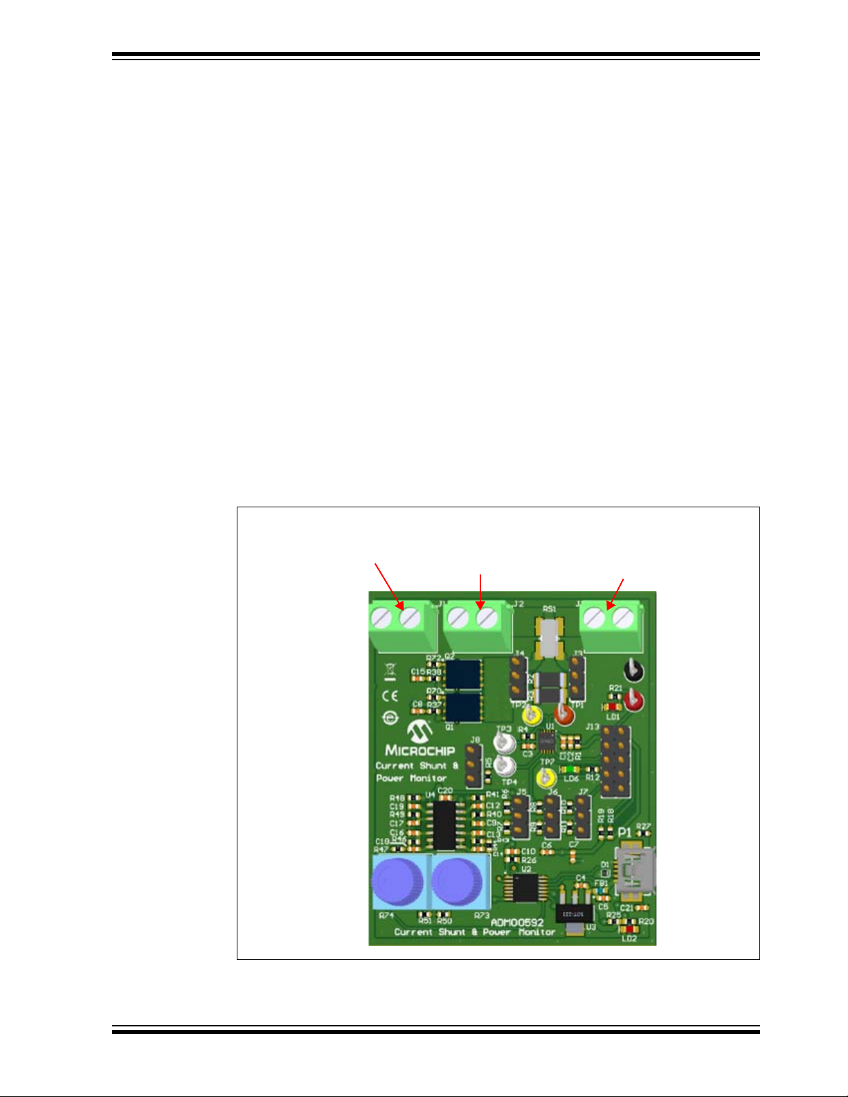
1.3.1 Board Layout
The evaluation board was designed for ease of use and user experimentation.
Figure 1-2 shows the top silkscreen for the board.
FIGURE 1-2: PAC1921 High-Side Current/Power Sensor Evaluation Board – Top Silkscreen.
DS50002376A-page 12 2015 Microchip Technology Inc.
Page 13

Product Overview
1.4 WHAT THE PAC1921 HIGH-SIDE CURRENT/POWER SENSOR EVALUATION BOARD KIT CONTAINS
This PAC1921 High-Side Current/Power Sensor Evaluation Board kit includes:
• PAC1921 High-Side Current/Power Sensor Evaluation Board (ADM00592)
• Supplied USB Mini Connector Cable
• Important Information Sheet
2015 Microchip Technology Inc. DS50002376A-page 13
Page 14

PAC1921 High-Side Current/Power Sensor Evaluation Board User’s Guide
NOTES:
DS50002376A-page 14 2015 Microchip Technology Inc.
Page 15

HIGH-SIDE CURRENT/POWER SENSOR
EVALUATION BOARD USER’S GUIDE
Chapter 2. Installation and Operation
2.1 GETTING STARTED
2.1.1 System Requirements
To use the PAC1921 High-Side Current/Power Sensor Evaluation Board, the following
are required:
•A PC running the Microsoft
• A display resolution of 800x600 or larger, for viewing several windows
simultaneously
• An available USB port
2.2 INSTALLING THE EVALUATION BOARD SOFTWARE
Follow these steps in order to install the board’s Graphical User Interface (GUI):
1. Download the software archive from the board’s web page, unzip it and
double-click the Setup.exe to start the installation. Figure 2-1 shows the initial
installation screen, which displays briefly as the setup program loads.
®
Windows® operating system
PAC1921
FIGURE 2-1: Software Installation – Initialize Window.
2015 Microchip Technology Inc. DS50002376A-page 15
Page 16

PAC1921 High-Side Current/Power Sensor Evaluation Board User’s Guide
2. Click Next in the Destination Directory window, shown in Figure 2-2. For proper
operation, the files must be installed in the default locations. The default location
for the software files is C:\Program Files (x86)\Microchip\PAC1921
and for the LabVIEW™ software is C:\Program Files\
National Instruments.
FIGURE 2-2: Software Installation – Setting the Destination Directory.
DS50002376A-page 16 2015 Microchip Technology Inc.
Page 17

Installation and Operation
3. Read and accept the license agreement, then click Next.
FIGURE 2-3: Software Installation – Software License Agreement.
4. To use the LabVIEW software, read and accept the license agreement, then click
Next.
FIGURE 2-4: Software Installation – LabVIEW™ Software License Agreement.
2015 Microchip Technology Inc. DS50002376A-page 17
Page 18

PAC1921 High-Side Current/Power Sensor Evaluation Board User’s Guide
5. Follow the on-screen instructions to complete the installation. During installation,
shortcuts will be created on the Windows Start Menu under Programs>
and on the desktop.
PAC1921
FIGURE 2-5: Software Installation – LabVIEW™ Software Installation Screen.
FIGURE 2-6: Software Installation – LabVIEW™ Software Installation Complete.
DS50002376A-page 18 2015 Microchip Technology Inc.
Page 19
Installation and Operation
When the installation is complete, the program will automatically run (see Figure 2-7).
FIGURE 2-7: PAC1921 GUI Start-up Screen.
2.3 MICROCHIP USB BRIDGE INSTALLATION
Connect the USB mini connector to the evaluation board and the standard USB connector to any available USB port on the PC. If the Microchip USB bridge driver has not
previously been installed on the selected USB port, download the MCP2221 Windows
driver and installer from www.microchip.com at:
http://www.microchip.com/wwwproducts/Devices.aspx?product=MCP2221
Follow the on-screen instructions to complete the installation process.
2015 Microchip Technology Inc. DS50002376A-page 19
Page 20

PAC1921 High-Side Current/Power Sensor Evaluation Board User’s Guide
NOTES:
DS50002376A-page 20 2015 Microchip Technology Inc.
Page 21

Chapter 3. Hardware Description
3.1 INTRODUCTION
The PAC1921 High-Side Current/Power Sensor Evaluation Board provides the means
to evaluate features, and to view and modify registers. There are two modes for using
the evaluation board:
• Demo mode: Monitors an on-board power source
• Sys mode: Monitors an external power source
LEDs indicate status information and test points are included to monitor system
voltages with a user-provided voltmeter or oscilloscope.
The PAC1921 device is an SMBus-compliant, high-side current/power monitor in a
10-pin, 3 mm x 3 mm DFN package. For details regarding the PAC1921 device, refer
to the “PAC1921 Data Sheet” (DS20005293).
3.1.1 Power Source
The board requires only one Universal Serial Bus (USB) connection to power the
board. USB bus voltage is provided to the on-board test power sources and the
USB-to-SMBus bridge. The evaluation board circuitry uses the on-board regulator to
regulate the +5V USB power to +3.3V.
PAC1921
HIGH-SIDE CURRENT/POWER SENSOR
EVALUATION BOARD USER’S GUIDE
3.2 USB-TO-SMBus BRIDGE
The USB-to-SMBus is based on the MCP2221 USB-to-I2C™ protocol converter, which
provides the interface between the USB and the SMBus. Power is sourced to the
microcontroller from the USB interface for device power and communication.
3.2.1 Direct SMBus Connect Option
It is also possible to connect an external SMBus master to the PAC1921 High-Side
Current/Power Sensor Evaluation Board. A few modifications to the board are
required, as explained below:
• Remove the jumpers on J13 and connect the SMBus master to the
SMBus_DATA, SMBus_CLK and #READ/INT pins, as well as an external supply
for +3.3V. Note that a return is also provided on this header for convenience
(GND).
• The +3.3V can be supplied by the SMBus bridge by leaving the +3.3V jumper in
place and retaining the USB connection.
2015 Microchip Technology Inc. DS50002376A-page 21
Page 22
PAC1921 High-Side Current/Power Sensor Evaluation Board User’s Guide
LED 1
V
DD
Power
LED 2
USB Power
LED 6
READ/INT
3.3 OPERATING MODE
3.3.1 SMBus Mode
By default, the evaluation board is configured so that the PAC1921 operates in SMBus
mode with an SMBus address of, 1001_100xb (98h). The address can be changed to
1001_101xb (9Ah) by moving jumper J8 to position 2-3. Cycle power to the evaluation
board in order for the change to take effect.
3.4 LED INDICATORS
LED locations are indicated in Figure 3-1.
FIGURE 3-1: LED Indicator Locations.
LEDs indicate the status of the signals, as described in Ta bl e 3- 1:
TABLE 3-1: LED STATUS INDICATORS
LED Signal OFF Green Red
LD1 V
LD2 +5V USB Power USB power is not present N/A +5V USB power is
LD6 READ/INT Pin is not asserted
DS50002376A-page 22 2015 Microchip Technology Inc.
Power VDD is not present N/A VDD is present
DD
(Read State)
Pin is asserted
(Integrate State)
present
N/A
Page 23
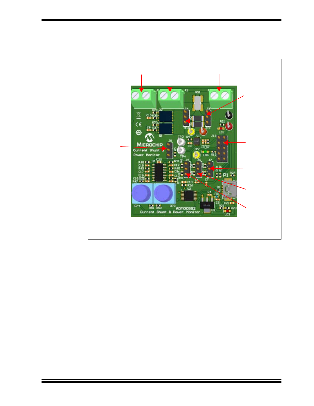
3.5 JUMPER SETTINGS
J11
GND
J2
V
SOURCE-
J1
V
SOURCE+
J3
Demo Sys
J4
Demo Sys
J13
Connections
J5
Reserved
J6
Reserved
J7
Reserved
J8
ADDR/SEL
Note: Refer to Appendix A. “Schematic and Layouts” to see the
connections of each jumper position.
This evaluation board has pin headers and jumper configurations to evaluate the
features of the PAC1921. Jumper locations are indicated in Figure 3-2.
Hardware Description
FIGURE 3-2: Jumper and External Connection Locations.
2015 Microchip Technology Inc. DS50002376A-page 23
Page 24
PAC1921 High-Side Current/Power Sensor Evaluation Board User’s Guide
Jumper settings are described in Tab le 3 - 2.
TABLE 3-2: JUMPER SETTINGS
Pin
Header
J1, J2 Vsource+, Vsource- External power source terminals. (See Section 3.8.2 “Load Connection”.)
J3, J4 Demo Sys Select Demo mode R
J5, J6, J7Reserved Reserved for future use
Label Default Position Alternate Position(s)
Positions 3-2 are jumpered on both
SENSE+/-
jumpers. (See Section 3.7 “Demo
Mode Setup and Operation”.)
.
Select Sys mode R
Positions 1-2 are jumpered on both
jumpers. (See Section 3.8 “Sys Mode
Setup and Operation”.)
SENSE+/-
.
J8 J8 (ADDR_SEL)
(See
Section 3.3.1 “SMBus
Mode”)
J11 GND Connect ground from external source for
J13 GND, #READ/INT,
SMBus_DATA,
SMBus_CLK, VDD
In SMBus mode, sets SMBus address to
1001_100b at power-up.
Positions 1-2 are jumpered.
USB bridge generates on-board 3.3V
and provides SMBus host.
Positions 1-2, 3-4, 5-6, 7-8, 9-10 are all
jumpered.
In SMBus mode, sets SMBus address to
1001_101b at power-up.
Positions 2-3 are jumpered.
Sys mode.
(See Section 3.2.1 “Direct SMBus
Connect Option”.)
3.6 TEST POINTS
The PAC1921 High-Side Current/Power Sensor Evaluation Board provides test points
for ground reference and signal access. Table 3-3 summarizes these test points.
TABLE 3-3: TEST POINTS
Test Point Marking Signal Function Monitored
1 Vsense+ (orange) SENSE+
2 Vsense- (yellow) SENSE-
3 OUT (white) OUT Pin
4 ADDR_SEL SMBus Address Select
5 Vdd (red) V
6 GND (black) Ground
7 #READ/INT (yellow) READ
DD
/INT Pin
DS50002376A-page 24 2015 Microchip Technology Inc.
Page 25
3.7 DEMO MODE SETUP AND OPERATION
J11 GND
Connect to
System Ground
J2 V
SOURCE-
Connect to
System DC
Load or Supply
J1 V
SOURCE+
Connect to
System DC
Load or Supply
Demo mode uses an on-board current source to exercise and demonstrate the features
of the PAC1921 power monitor. The 100 mV constant-current source is provided using
a +5V USB as the supply. Parallel sense resistors are provided to convert the current
to a corresponding voltage for the PAC1921 to read at the SENSE+ and SENSEinputs. The evaluation board is assembled with jumpers J3 and J4 positioned for Demo
mode (see Section 3.5 “Jumper Settings”). Current is controlled by the evaluation
board Demo Configuration section of the evaluation board GUI (see
Section 4.2.6 “EVB Demo Configuration Panel”).
3.8 SYS MODE SETUP AND OPERATION
Sys mode uses external current sources to exercise and demonstrate the features of
the PAC1921 power monitor.
3.8.1 Jumper Positions
To use Sys mode, reposition jumpers J3 and J4 (see Table 3-2) to disconnect the
on-board demonstration current sources.
3.8.2 Load Connection
Hardware Description
A 5 milliohm (1% tolerance) sense resistor, connected between J1 and J2, is provided
on-board the PAC1921 evaluation board to measure system current.
Load connections to the system can be established, as shown in Figure 3-3.
.
.
FIGURE 3-3: Load Connection Location.
2015 Microchip Technology Inc. DS50002376A-page 25
Page 26

PAC1921 High-Side Current/Power Sensor Evaluation Board User’s Guide
NOTES:
DS50002376A-page 26 2015 Microchip Technology Inc.
Page 27

4.1 OVERVIEW
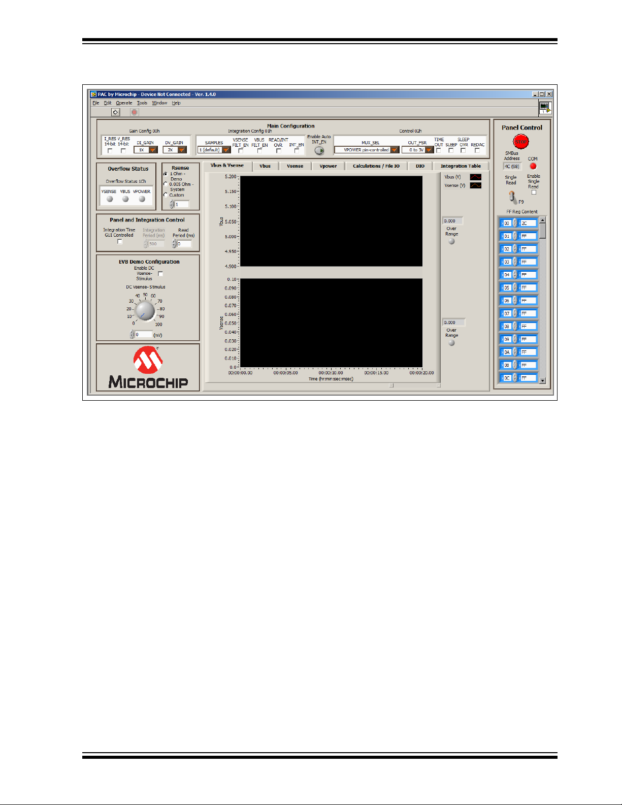
Panel Control
Main Configuration Panel
Panel and Integration Control
Rsense Option Panel
EVB Demo Configuration Panel
Configuration/View Tabs
Overflow Status Panel
To get the Graphical User Interface (GUI) and the Evaluation Board (EVB) running,
follow these instructions:
1. Start the PAC1921 GUI software: from the Windows Start menu, select
2. Connect the USB mini connector end of the cable to the board and the standard
The PAC1921 High-Side Current/Power Sensor Evaluation Board Graphical User
Interface (GUI) is shown in Figure 4-1.
PAC1921
HIGH-SIDE CURRENT/POWER SENSOR
EVALUATION BOARD USER’S GUIDE
Chapter 4. Software Description
Programs
USB connector of the cable to any available USB port on the PC. The V
USB power LEDs (LD1 and LD2, respectively) will illuminate RED, indicating that
the PAC1921 is powered up and the MCP2221 USB bridge is connected to the PC.
>PAC1921.
DD
and
FIGURE 4-1: GUI Interface Panel.
2015 Microchip Technology Inc. DS50002376A-page 27
Page 28

PAC1921 High-Side Current/Power Sensor Evaluation Board User’s Guide
When the evaluation board is connected or disconnected, a message displays as
shown in Figure 4-2. With the evaluation board connected, click Auto-detect Address
to restart communications.
FIGURE 4-2: Communications Failure Message.
4.1.1 Tips for Using the Evaluation Board GUI
• After a power-up of the evaluation board, the default settings are loaded. Users
can save the setting configurations to user-named files, which can be reloaded at
any time for quick reconfiguration (see Section 4.3.3.1 “Configuration Save and
Load”).
• To configure the GUI and PAC1921 for free-run integration power measurement,
press the <F2> function key on the keyboard.
• To reload the PAC1921 register defaults, press the <F6> function key on the
keyboard.
• When using the GUI, the PAC1921 can enter a Sleep state; however, it wakes to
service the GUI SMBus communications, then returns to Sleep. For this reason,
the current consumption will be slightly higher than expected in Sleep state when
using the GUI.
• When the PAC1921 enters Sleep state, the PAC1921 clears the measurement
registers, and consequently, the GUI Calculations/File IO tab is cleared. To
prevent the PAC1921 from entering Sleep, check the “SLEEP OVR” box in the
Main Configuration section.
DS50002376A-page 28 2015 Microchip Technology Inc.
Page 29

4.2 INTERFACE DESCRIPTION AND OPERATION
COM Status
Indicator
SMBus
Address
Indicator
Stop Button
Enable Single
Read Option
Register Content
Run Button
4.2.1 Panel Control Section
The Panel Control section on the right side of the GUI, shown in Figure 4-3, affects the
GUI operation.
Software Description
FIGURE 4-3: Panel Control Section.
4.2.1.1 STOP AND RUN BUTTONS
Pressing the Stop button, as shown in Figure 4-3, interrupts the GUI software communications with the evaluation board. When the Stop button is clicked, the Run button is
displayed on the menu bar (see Figure 4-4).
FIGURE 4-4: Run Button.
2015 Microchip Technology Inc. DS50002376A-page 29
Page 30

PAC1921 High-Side Current/Power Sensor Evaluation Board User’s Guide
SMBus
Address
Indicator
COM Status
Indicator
Single Read
Button
To restart the communication between the software and the evaluation board, click the
Run button. The arrow button disappears when the communications resume.
Note 1: Stopping and restarting the GUI does not affect register settings. To
restore default register settings, disconnect power from the evaluation
board, then reconnect power.
2: Stopping the GUI clears the “Enable DC Vsense- Stimulus” box (see
Section 4.2.6 “EVB Demo Configuration Panel”).
To close the program, use the Close (X) button in the upper right corner of the window.
4.2.1.2 SMBus ADDRESS
The “SMBus Address” box, shown in Figure 4-5, indicates the selected SMBus
address. The SMBus address can be changed by moving a jumper (see
Section 3.3.1 “SMBus Mode”).
FIGURE 4-5: SMBus Address Indicator.
4.2.1.3 COM STATUS INDICATOR
The “COM” status indicator, on the right side of the panel as shown in Figure 4-5,
indicates the status of communications over the SMBus. During normal operation, the
“COM” indicator is black. If the SMBus communications fail, the “COM” indicator turns
red.
4.2.1.4 SINGLE READ/CONTINUOUS READ
The panel defaults to continuous register reads (toggle switch in down position, as
shown in Figure 4-5). To stop continuous register reads, check the “Enable Single
Read” box. In order to capture the register values at a given time, click the switch, which
will briefly flip to “Single Read”.
4.2.1.5 REGISTER CONTENT
“Reg Content”, shown in Figure 4-3, is a scrollable list of the PAC1921 registers and
the last read value. It is important to note that not all addresses are physical memory
locations on the device; these registers will read ‘0’. Likewise, some registers shown
(undocumented in the data sheet) may have data. Editing these registers can cause
unexpected results.
To update a register value, locate the register address in the left column, type the new
value in the corresponding cell in the right column, and press Enter on the keyboard or
click on another part of the GUI.
DS50002376A-page 30 2015 Microchip Technology Inc.
Page 31

Software Description
4.2.1.5.1 Numbering Systems Views
The “Reg Content” section allows values to be displayed using different numbering
systems: Decimal, Hex, Octal, Binary or SI Notation.
To view a value using a different numbering system, click the indicator to the left of the
value in the cell, shown circled in Figure 4-6.
FIGURE 4-6: Numbering System Indicators.
4.2.2 Main Configuration Panel
The Main Configuration section, shown in Figure 4-7, contains the PAC1921 configuration controls in registers 00h, 01h and 02h. Refer to the data sheet for register bit
descriptions.
FIGURE 4-7: Main Configuration Panel.
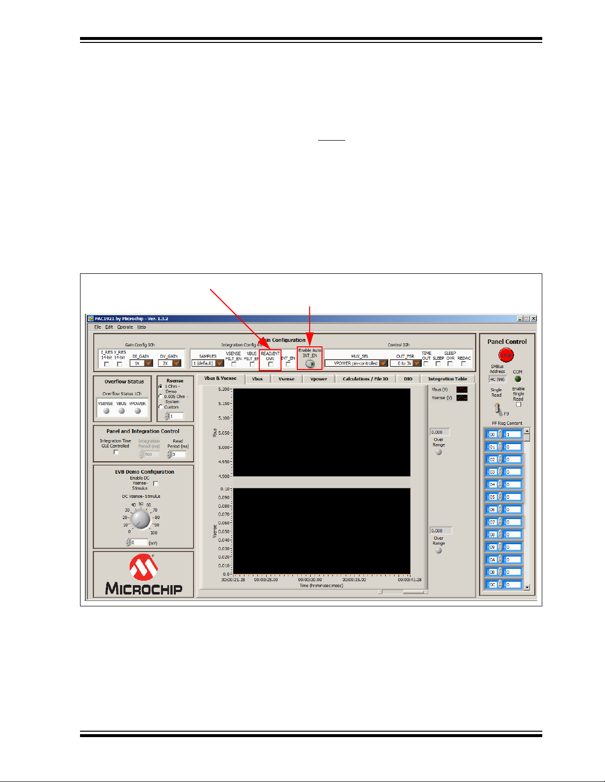
4.2.2.1 ENABLE AUTO INT_EN
The “Enable Auto INT_EN” control is a GUI control convenience. Under normal
operation, for most of the integration parameter settings, changes do not take effect
until the PAC1921 is placed in the Read state. When the “Enable Auto INT_EN” control
is activated (light green – shown as “Enabled” in Figure 4-8), it automatically places the
PAC1921 into the Read state and back to Integrate state whenever a Main Configuration control is changed. It also updates the GUI calculations. When the
“Enable Auto INT_EN” control is disabled (dark green), the user must place the device
in the Read state before the “I_RES”, “V_RES”, “SAMPLES”, “VSENSE FILT_EN” and
“VBUS FILT_EN” changes take effect, and to update the GUI calculations.
It is recommended that the “Enable Auto INT_EN” control be activated when using
the GUI.
FIGURE 4-8: Enable Auto INT_EN GUI Control.
2015 Microchip Technology Inc. DS50002376A-page 31
Page 32
PAC1921 High-Side Current/Power Sensor Evaluation Board User’s Guide
“READ/INT OVR” Box is Checked
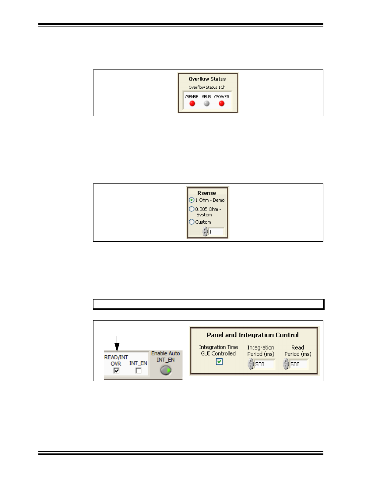
4.2.3 Overflow Status Panel
The Overflow Status section, shown in Figure 4-9, represents the three bits in the
Overflow Status Register 1Ch. When an indicator turns red, it indicates an overflow.
FIGURE 4-9: Overflow Status.
4.2.4 Rsense Panel
The Rsense section, shown in Figure 4-10, needs to reflect the value of the R
resistor in use on the evaluation board. This value is used in calculations done by the
GUI. In Demo mode, select the 1 Ohm - Demo button. In Sys mode, select the
0.005 Ohm - System button. If another resistor is used, check the Custom option
button and fill the corresponding value in the spin box underneath the option.
FIGURE 4-10: Rsense Configuration Panel.
SENSE
4.2.5 Panel and Integration Control Panel
The Panel and Integration Control section, shown in Figure 4-11, contains GUI controls
which set and clear the INT_EN bit. When using these controls, check the “READ/INT
OVR” box in the Main Configuration section to allow the INT_EN bit to override the
READ
/INT pin state.
Note: Read Period (ms) is always enabled.
DS50002376A-page 32 2015 Microchip Technology Inc.
FIGURE 4-11: Panel and Integration Control.
Page 33
Software Description
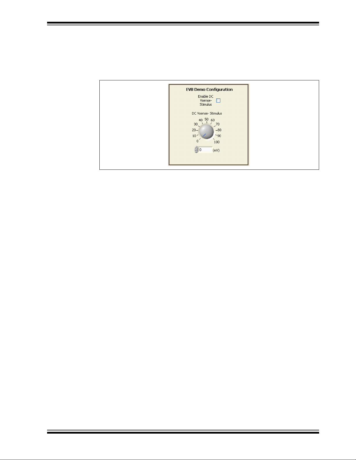
4.2.6 EVB Demo Configuration Panel
The EVB Demo Configuration panel, shown in Figure 4-12, contains GUI controls
which affect the Demo mode. To inject current onto V
Vsense- Stimulus” box. To set the current level, rotate the “DC Vsense- Stimulus” dial
or type a value between 0 and 100 in the (mV) spin box below the dial.
FIGURE 4-12: Evaluation Board Demo Configuration.
SENSE-
, check the “Enable DC
2015 Microchip Technology Inc. DS50002376A-page 33
Page 34
PAC1921 High-Side Current/Power Sensor Evaluation Board User’s Guide
Click to enter new values to scale the plot.
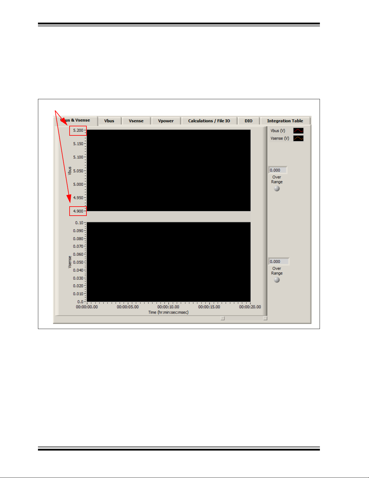
4.3 TAB DESCRIPTIONS
4.3.1 Vbus & Vsense Tab
The Vbus & Vsense tab, shown in Figure 4-13, displays plots for calculated V
volts and calculated V
in volts. The plots are not self-scaling. If the value in the
SENSE
BUS
in
box at the right of the plot (indicated with arrows) falls outside the Y-axis range on the
plot, click the top and/or bottom value on the axis and type in a new value.
FIGURE 4-13: Vbus & Vsense Tab.
DS50002376A-page 34 2015 Microchip Technology Inc.
Page 35
Software Description
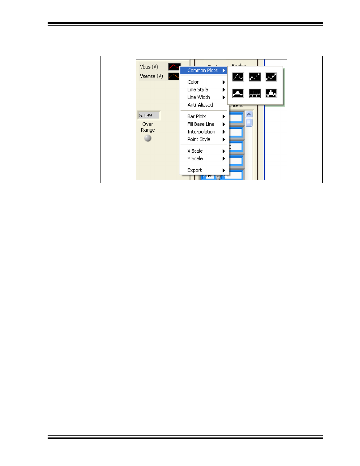
To change the look of the plot lines, click the applicable graphic in the legend on the
right of the tab to display a menu of options, as shown in Figure 4-14.
FIGURE 4-14: Plot Legend Context Menu.
4.3.2 Vbus, Vsense and Vpower Tabs
There are separate tabs to show individual plots for Vbus, Vsense and Vpower. They
operate similarly to the Vbus & Vsense tab described above.
2015 Microchip Technology Inc. DS50002376A-page 35
Page 36
PAC1921 High-Side Current/Power Sensor Evaluation Board User’s Guide
1LSB
0.1V
RDI_GAIN
------------ ------------- ------------ ---
32V
DV_GAIN
------------- --------------
1023 2
6
------------- ------------- ------------- ---------- ------------- ------------=
Where:
1LSB = LSB value in watts for V
POWER
Result Registers 1Dh and 1Eh
0.1V = Maximum V
SENSE
voltage
R=Value of R
SENSE
resistor in ohms
DI_GAIN = Digital current gain
32V/DV_GAIN = Maximum voltage
1023 = (210 – 1) = 10-bit FSR
2
6
= Adjustment for 6 unused register bits when read as a 16-bit number
4.3.3 Calculations/File IO Tab
The Calculations/File IO tab, shown in Figure 4-15, displays register data (in decimal
by default). It also shows calculated results which were obtained by applying the data
sheet equations to the register data.
DS50002376A-page 36 2015 Microchip Technology Inc.
FIGURE 4-15: Calculations/File IO Tab.
An example of using the equations to calculate power is as follows.
The value of one LSB in the V
Result registers, in watts, can be calculated
POWER
according to Equation 4-1.
EQUATION 4-1: LSB CALCULATION
Page 37
Software Description
0.1V
1
1
------------- ----
32V
1
----------
1023
------------ ------------- ---------42 0.13138W=
Where:
0.1V = Maximum V
SENSE
voltage
1 = Value of R
SENSE
resistor
1 = Digital current gain
32V/1 = Maximum voltage
1023 = 10-bit FSR
42 = Decimal value of V
POWER
Result Registers 1Dh and 1Eh
The power calculation using the V
POWER
Result registers value from Figure 4-15 is
shown in Equation 4-2.
EQUATION 4-2: POWER CALCULATION
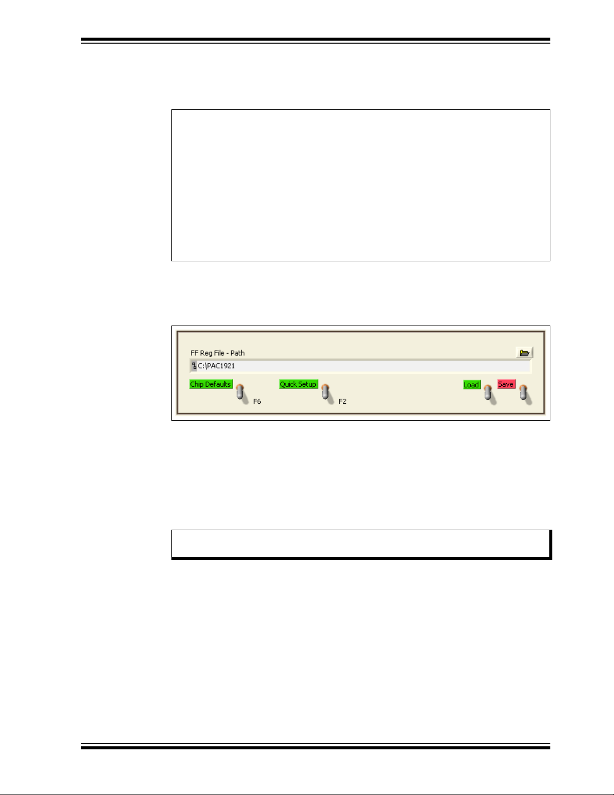
4.3.3.1 CONFIGURATION SAVE AND LOAD
The Calculations/File IO tab contains controls, as shown in Figure 4-16, which save the
settings currently configured in the PAC1921 to allow quick reconfiguration at any time.
2015 Microchip Technology Inc. DS50002376A-page 37
FIGURE 4-16: Save/Load Section.
To save configuration settings, configure the PAC1921 as desired, then display the
Calculations/File IO tab. The “FF Reg File Path” box defaults to where the GUI software is installed. To change the location, type in a path, or click the folder icon to use
a Windows
file will be saved. The file should be named with the.txt extension or similar text file
format. Once a file name and location have been chosen, click the Save switch, and
the file is saved.
Note: If a file with the same name already exists, the file will be overwritten
The data is saved in two columns, separated by tabs. The first column is the register
address and the second column is the register data.
Once a file is saved, it can be recalled at any time by selecting the file in the “FF Reg
File Path” box and clicking the Load switch.
Click the Chip Defaults switch or press the <F6> function key on the keyboard to
reload register defaults on the PAC1921.
®
system-based navigation aid to select the folder where the configuration
without warning and old data will be lost.
Page 38
PAC1921 High-Side Current/Power Sensor Evaluation Board User’s Guide
Click the Quick Setup switch or press the <F2> function key on the keyboard to set up
the GUI and PAC1921 for free-run integration power measurement. The Quick Setup
switch does the following:
- Enables the “Enable Auto INT_EN” option.
- Enables the “READ/INT OVR” option.
- Enables the “INT_EN” option.
- Sets “MUX_SEL” to VPOWER free-run.
- Enables the “Enable DC Vsense- Stimulus” option.
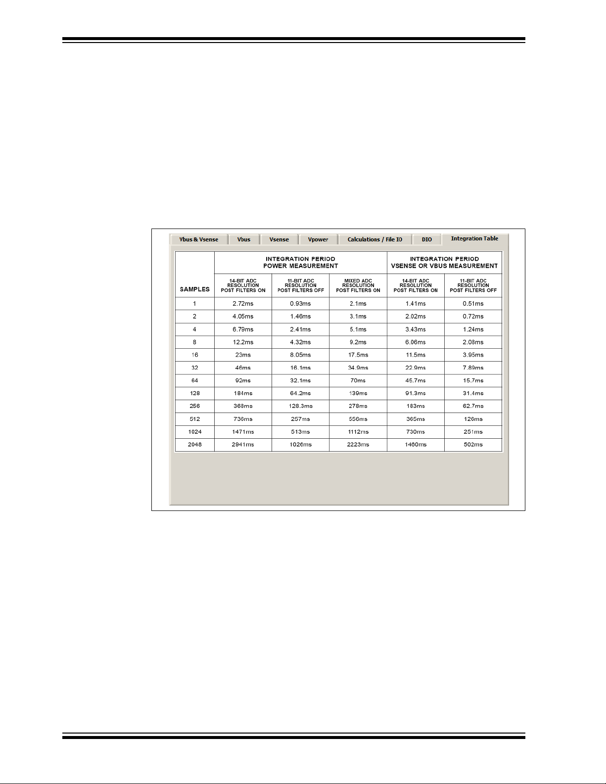
4.3.4 Integration Table Tab
The Integration Table tab, shown in Figure 4-17, shows the maximum integration
periods for a selected number of samples with various settings.
FIGURE 4-17: Integration Table Tab.
DS50002376A-page 38 2015 Microchip Technology Inc.
Page 39
4.4 EVALUATION BOARD EXAMPLES
Check the “READ/INT OVR” Box
Check the “Enable Auto INT_EN” Control
4.4.1 Power Pin-Controlled Integration Example
This example provides steps to experiment with pin-controlled integration in SMBus
mode and see the effects of gain.
1. In the Main Configuration section, check the “READ/INT OVR” box. This allows
the INT_EN bit to override the READ
INT_EN” control to set automatic GUI updates.
2. In the Panel and Integration Control section, check the “Integration Time GUI
Controlled” box, and set the “Read Period (ms)” to 500 ms. This causes the
INT_EN bit to toggle between high for 500 ms (putting the PAC1921 in the
Integrate state) and low for 500 ms (putting the device in the Read state).
3. In the EVB Demo Configuration section, check the “Enable DC Vsense-
Stimulus” box and type 40 mV in the “DC Vsense- Stimulus (mV)” box.
4. Observe the plots on the Vbus & Vsense tab, as shown in Figure 4-18. The
evaluation board demo V
BUS
/INT pin state. Also check the “Enable Auto
is ~5.1V and V
Software Description
is ~0.04V.
SENSE
FIGURE 4-18: Pin-Controlled Integration, No Gain.
2015 Microchip Technology Inc. DS50002376A-page 39
Page 40
PAC1921 High-Side Current/Power Sensor Evaluation Board User’s Guide
5. Observe the data on the Calculations/File IO tab, as shown in Figure 4-19.
FIGURE 4-19: Pin-Controlled Integration without Gain.
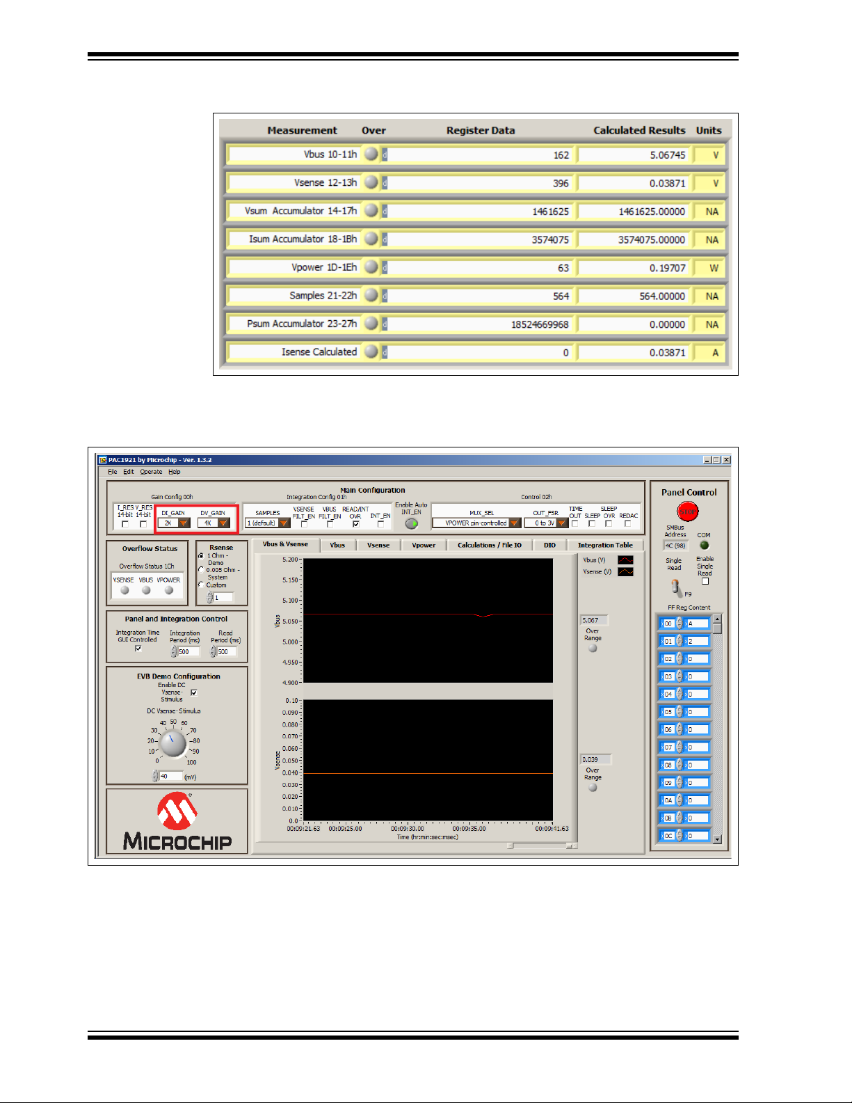
6. To see the effects of gain, change “DI_GAIN” to 2X and “DV_GAIN” to 4X in the
Gain Config 00h section, as shown in Figure 4-20.
FIGURE 4-20: Pin-Controlled Integration with Gain.
DS50002376A-page 40 2015 Microchip Technology Inc.
Page 41
Software Description
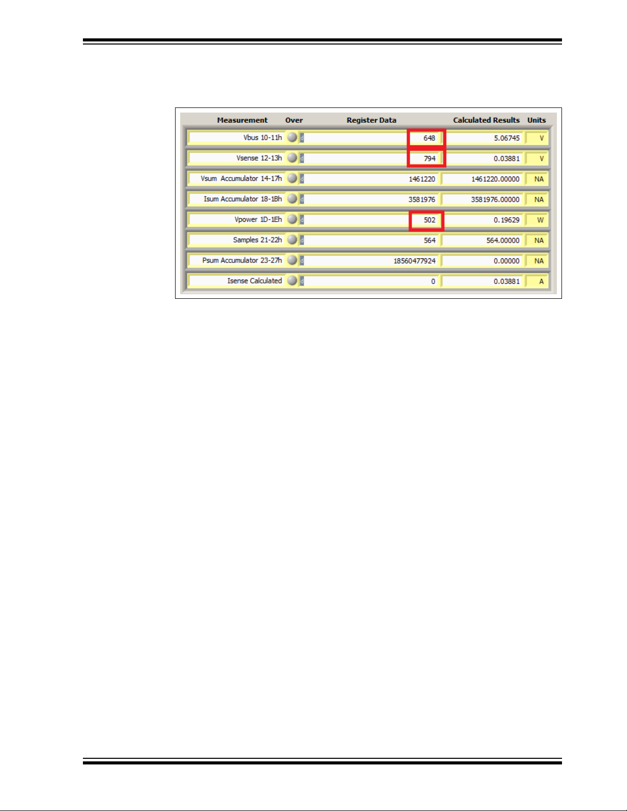
7. Observe the data on the Calculations/File IO tab, as shown in Figure 4-21.
Notice that the Register Data values (with the exception of the accumulators)
reflect the gain.
FIGURE 4-21: Pin-Controlled Integration with Gain.
2015 Microchip Technology Inc. DS50002376A-page 41
Page 42

PAC1921 High-Side Current/Power Sensor Evaluation Board User’s Guide
4.4.2 Power Free-Run Integration Example
This section provides steps to experiment with free-run integration in SMBus mode and
see the effects of filtering, resolution and sampling. It starts by showing the fastest
integration period and progressively shows higher accuracy.
1. Press the <F2> function key on the keyboard. This performs Quick Setup, which
checks the “READ/INT OVR” box, the “INT_EN” bit box and the “Enable DC
Vsense- Stimulus” box, enables the “Enable Auto INT_EN” control and sets
“MUX_SEL” to VPOWER free-run. Integration begins using the 1 sample default.
2. In the Main Configuration section, click the “I_RES” and “V_RES” boxes so 11-bit
shows; this lowers the resolution from 14 bits to 11 bits.
3. In the Main Configuration section, uncheck the “VSENSE FILT_EN” and “VBUS
FILT_EN” boxes to disable the ADC post filters.
4. In the EVB Demo Configuration section, type 40 mV in the “DC VsenseStimulus” spin box.
5. Observe the plots on the Vbus & Vsense tab, as shown in Figure 4-22, adjusting
the Y-axis values as desired. These settings result in the shortest integration
period.
FIGURE 4-22: Free-Run Integration, Shortest Period.
DS50002376A-page 42 2015 Microchip Technology Inc.
Page 43

Software Description
6. Check the “VSENSE FILT_EN” and “VBUS FILT_EN” boxes to enable the ADC
post filters, and observe the improvement in the plots on the Vbus & Vsense tab,
as shown in Figure 4-23.
FIGURE 4-23: Free-Run Integration with ADC Post Filters Enabled.
2015 Microchip Technology Inc. DS50002376A-page 43
Page 44

PAC1921 High-Side Current/Power Sensor Evaluation Board User’s Guide
7. Uncheck the “I_RES” and “V_RES” boxes to enable 14-bit resolution, and
observe the improvement in the plots on the Vbus & Vsense tab, as shown in
Figure 4-24.
FIGURE 4-24: Free-Run Integration with 14-Bit Resolution.
DS50002376A-page 44 2015 Microchip Technology Inc.
Page 45

Software Description
8. Change the number of “SAMPLES” to 8 and observe the improvement in the
plots on the Vbus & Vsense tab, as shown in Figure 4-25.
FIGURE 4-25: Increased Sample Effect.
4.5 TROUBLESHOOTING
4.5.1 GUI Controls Unresponsive After Installation
Restart the computer. In some cases, a restart is required after installation.
4.5.2 GUI Freezes
If the GUI freezes for unknown reasons, communications cannot be stopped and the
program cannot be closed. Disconnect the USB cable from the evaluation board, then
close the program. Reconnect the evaluation board, then restart the GUI.
2015 Microchip Technology Inc. DS50002376A-page 45
Page 46

PAC1921 High-Side Current/Power Sensor Evaluation Board User’s Guide
NOTES:
DS50002376A-page 46 2015 Microchip Technology Inc.
Page 47

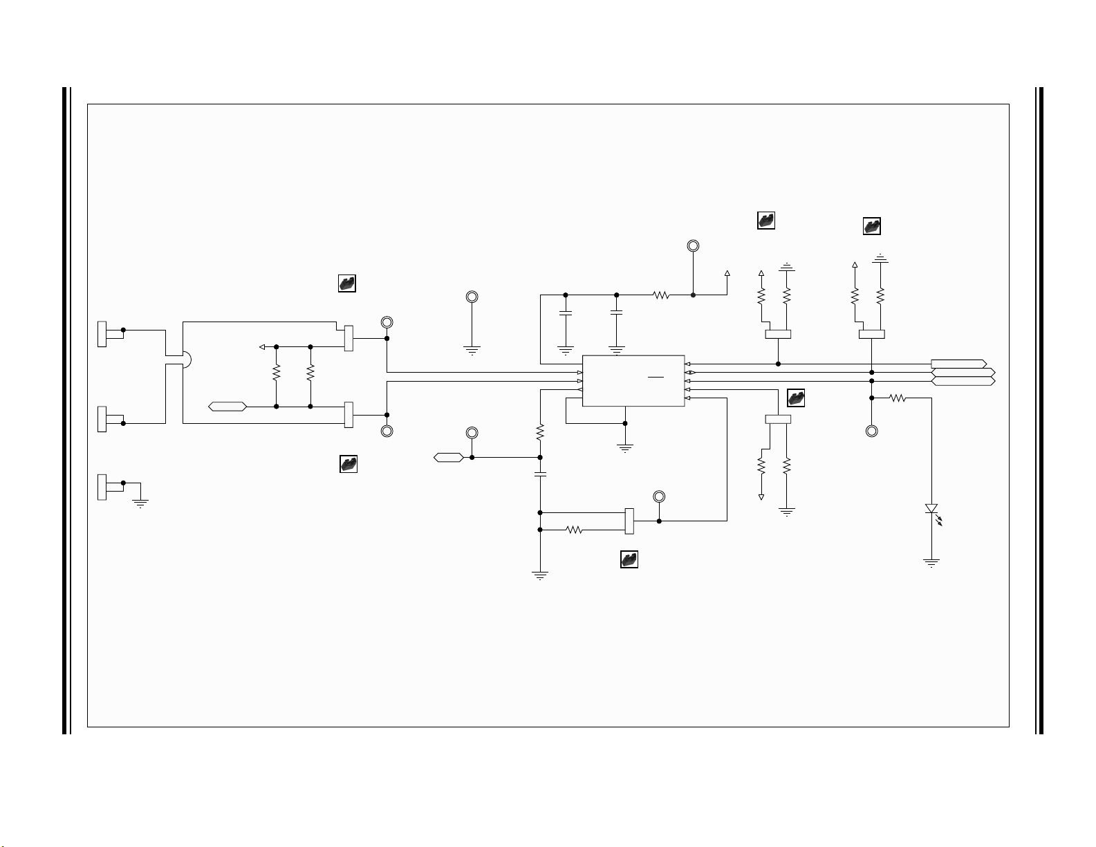
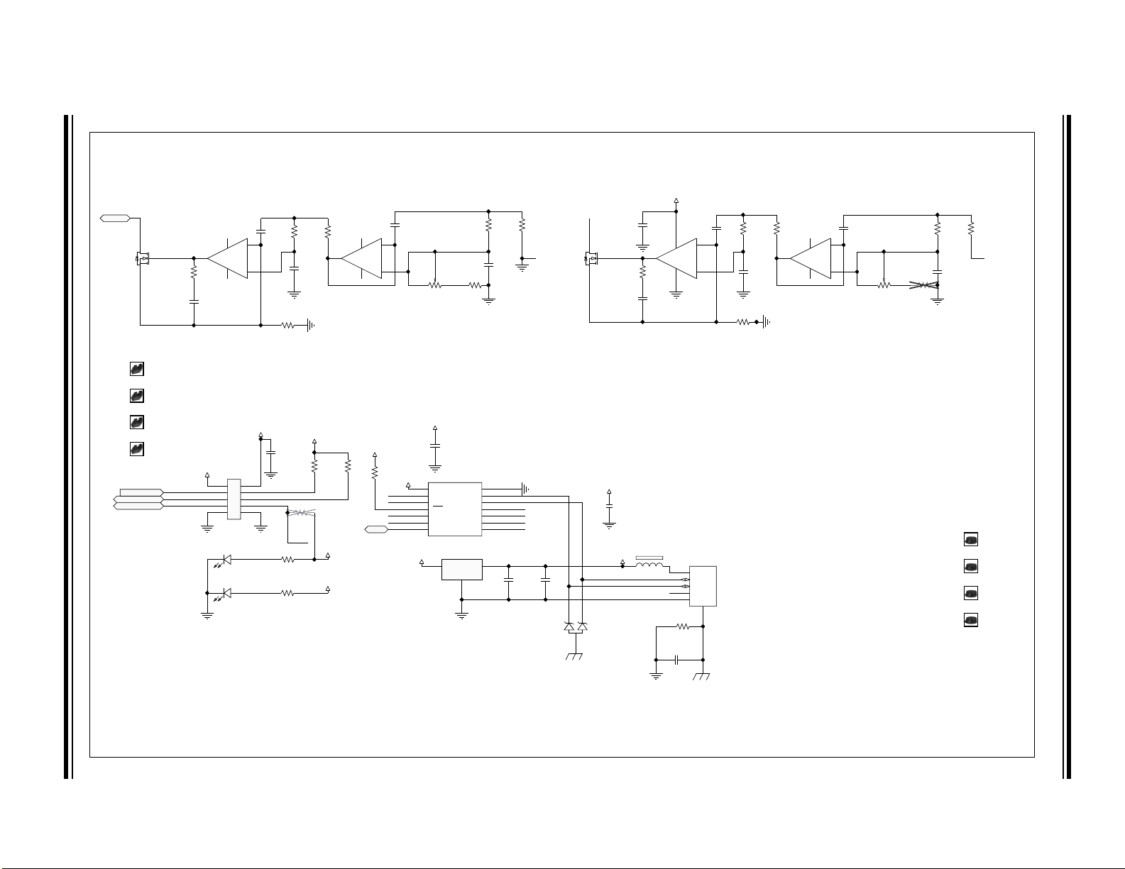
Appendix A. Schematic and Layouts
A.1 INTRODUCTION
This appendix contains the following schematics and layouts for the PAC1921
High-Side Current/Power Sensor Evaluation Board:
• Board – PAC1921 Current Shunt and Power Monitor Schematic
• Board – USB Bridge and Sig Gen Schematic
• Board – Top Silk
• Board – Top Copper and Silk
• Board – Top Copper
• Board – Bottom Copper
• Board – Bottom Copper and Silk
• Board – Bottom Silk
PAC1921
HIGH-SIDE CURRENT/POWER SENSOR
EVALUATION BOARD USER’S GUIDE
2015 Microchip Technology Inc. DS50002376A-page 47
Page 48
DS50002376A-page 48 2015 Microchip Technology Inc.
V
SENSE+
V
SENSE-
V
SOURCE-
V
SOURCE+
+5V_USB
V
DD
V
DD
V
DD
V
DD
Demo
Sys
Sys
V
SENSE+
V
SENSE-
Demo
Out
#READ/INT
#READ/INT
GND
J8, 1-2 C lose (default) = 1001_100xb -> 98h
J8, 2-3 Close (alternative) = 1001_101x b -> 9Ah
J8, Open (alternative) = Apply external resistor
for GAIN_SEL function in Stand- Alone mode.
Read the data sheet for more information
ADDR_SEL
/GAIN_SEL
V
DD
SMBUS_CLK
SMBUS_DATA
#READ/INT
IDEMO
Idemo
OUT
GP2
COMM_SEL
SMBus_CLK
SMBus_DATA
#READ/INT
TP LOOP Yellow
TP2
TP LOOP Orange
TP1
TP LOOP Black
TP6
TP LOOP White
TP3
TP LOOP White
TP4
TP LOOP Red
TP5
TP LOOP Yellow
TP7
EDZ250/2
J1
EDZ250/2
J2
EDZ250/2
J11
2R
2010
5%
R2
2R
2010
5%
R3
HDR-2.54 Male 1x3
J3
123
HDR-2.54 Male 1x3
J4
123
HDR-2.54 Male 1x3
J6
123
HDR-2.54 Male 1x3
J7
HDR-2.54 Male 1x3
J8
123
HDR-2.54 Male 1x3
J5
Shunt 2.54 mm 1x2 Handle
JP3
Shunt 2.54 mm 1x2 Handle
JP4
Shunt 2.54mm 1x2 Handle
JP5
Shunt 2.54 mm 1x2 Handle
JP6
Shunt 2.54mm 1x2 Handle
JP7
Shunt 2.54 mm 1x2 Handle
JP8
0.1 μF
16V
0603
C1
0.001 μF
50V
0603
C3
1 μF
16V
0603
C2
12.1k
0603
1%
R8
12.1k
0603
1%
R9
12.1k
0603
1%
R10
12.1k
0603
1%
R11
12.1k
0603
1%
R6
12.1k
0603
1%
R7
120R
0603
1%
R4
120R
0603
1%
R5
100R
0603
1%
R1
GREEN
LD6
2k
0603
1%
R12
V
DD
1
SENSE+
2
SENSE-
3
OUT
4
GND
5
ADDR_SEL
6
COMM_SEL
7
READ/INT
8
SM_DATA
9
SM_CLK
10
EP
11
PAC1921-1
U1
1 2
3
4
0.005R
1%
RS1
3 2 1
3 2 1
21
2121
PAC1921 High-Side Current/Power Sensor Evaluation Board User’s Guide
A.2 BOARD – PAC1921 CURRENT SHUNT AND POWER MONITOR SCHEMATIC
Page 49
2015 Microchip Technology Inc. DS50002376A-page 49
GP1 GP3
+3.3V
V
DD
+5V_USB
+5V_USB
V
DD
+5V_USB
Steady state current generator Waveform Current Generator
VDD Power
USB Power
OUT
IDEMO
#READ/INT
SMBUS_DATA
SMBUS_CLK
Idemo
Idemo
SMBus_CLK
SMBus_DATA
#READ/INT
SMBusCLK
SMBusDATA
ID
4
V
BUS
1
GND
5
D-
2
D+
3
0
USB MINI-B Female
P1
0.47 μF
6.3V
0603
C10
SMBusDATA
SMBusCLK
+3.3V
+3.3V
+3.3V
+3.3V
RX
TX
GP2 GP3
GP0
GP1
RESET +3.3V
+3.3V
+3.3V
GP0
Rubber Pad Cyl D7.9H5.3
PAD1
Rubber Pad Cyl D7.9H5.3
PAD2
Rubber Pad Cyl D7.9H5.3
PAD3
Rubber Pad Cyl D7.9H5.3
PAD4
DD+
V
BUS
1k
0603
1%
R20
1k
0603
1%
R21
12.1k
0603
1%
R18
12.1k
0603
1%
R19
12.1k
0603
1%
R26
1M
0603
1%
R27
3.32k
0603
1%
R44
12.1k
0603
1%
R41
7.5k
0603
1%
R43
12.1k
0603
1%
R50
15.4k
0603
1%
R40
20R
0603
1%
R70
120R
0603
1%
R37
3.32k
0603
1%
R47
12.1k
0603
1%
R48
7.5k
0603
1%
R46
12.1k
0603
1%
R51
15.4k
0603
1%
R49
20R
0603
1%
R72
120R
0603
1%
R38
0.022 μF
50V
0603
C14
2200 pF
50V
0603
C13
100 pF
50V
0603
C21
10 μF
10V
0603
C4
RED
LD2
RED
LD1
FB1
2200 pF
50V
0603
C12
2200 pF
50V
0603
C9
Shunt 2.54 mm 1x2 Handle
JP9
Shunt 2.54 mm 1x2 Handle
JP10
Shunt 2.54 mm 1x2 Handle
JP11
Shunt 2.54 mm 1x2 Handle
JP12
1 μF
16V
0603
C15
1 μF
16V
0603
C8
10 μF
10V
0603
C7
+A
3
-A
2
OUTA
1
V
SS
V
DD
11 4
MCP6004
U4A
+B
5
-B
6
OUTB
7
V
SS
V
DD
11 4
MCP6004
U4B
+C
10
-C
9
OUTC
8
V
SS
V
DD
11 4
MCP6004
U4C
+D
12
-D
13
OUTD
14
V
SS
V
DD
11 4
MCP6004
U4D
2
13
10k
3386F
10%
R73
2
1 3
10k
3386F
10%
R74
1
3
2
ESD5V3
D1
0.1 μF
16V
0603
C5
0.1 μF
16V
0603
C6
0.1 μF
16V
0603
C16
0.1 μF
16V
0603
C17
0.1uF
16V
0603
C18
0.1 μF
16V
0603
C19
0.1 μF
16V
0603
C20
V
IN
1
GND
2
V
OUT
3
MCP1825S/3.3V
U3
D
G
S
MCP87050
Q1
D
G
S
MCP87050
Q2
2k
0603
1%
R25
V
DD
1
GP0
2
GP1
3
RST
4
UART RX
5
UART TX
6
GP27GP3
8
SDA
9
SCL
10
V
USB
11
D-
12
D+
13
V
SS
14
MCP2221
U2
1
2
3
4
5
6
7
8
9
10
HDR-2.54 Male 2x5
J13
A.3 BOARD – USB BRIDGE AND SIG GEN SCHEMATIC
Schematic and Layouts
Page 50
PAC1921 High-Side Current/Power Sensor Evaluation Board User’s Guide
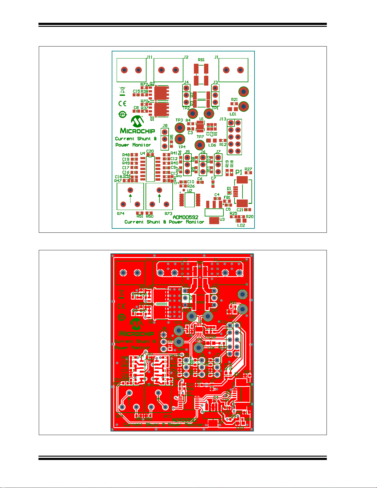
A.4 BOARD – TOP SILK
A.5 BOARD – TOP COPPER AND SILK
DS50002376A-page 50 2015 Microchip Technology Inc.
Page 51
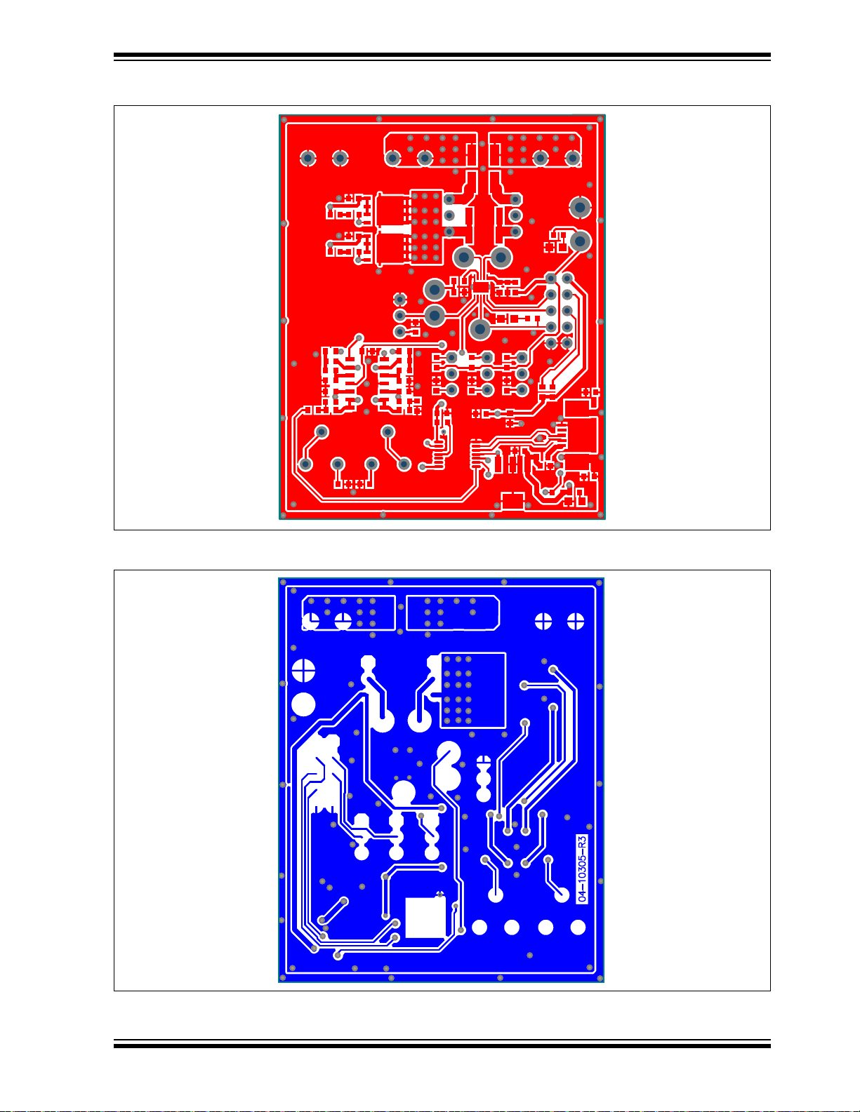
A.6 BOARD – TOP COPPER
Schematic and Layouts
A.7 BOARD – BOTTOM COPPER
2015 Microchip Technology Inc. DS50002376A-page 51
Page 52
PAC1921 High-Side Current/Power Sensor Evaluation Board User’s Guide
A.8 BOARD – BOTTOM COPPER AND SILK
A.9 BOARD – BOTTOM SILK
DS50002376A-page 52 2015 Microchip Technology Inc.
Page 53

HIGH-SIDE CURRENT/POWER SENSOR
EVALUATION BOARD USER’S GUIDE
Appendix B. Bill of Materials (BOM)
PAC1921
TABLE B-1: BILL OF MATERIALS (BOM)
Qty Reference Description Manufacturer Part Number
8 C1, C5, C6,
C16, C17,
C18, C19, C20
1 C10 Cap. Ceramic, 0.47 µF, 6.3V, 10%,
1 C14 Cap. Ceramic, 0.022 µF, 50V, 10%,
3 C2, C8, C15 Cap. Ceramic, 1 µF, 16V, 10%, X7R,
1 C21 Cap. Ceramic, 100 pF, 50V, 1%, C0G,
1 C3 Cap. Ceramic, 0.001 µF, 50V, 20%,
2 C4, C7 Cap. Ceramic, 10 µF, 10V, 20%, X5R,
3 C9, C12, C13 Cap. Ceramic, 2200 pF, 50V, 10%,
1 D1 DIO TVSARR, ESD5V3U2U, 5.3V,
1 FB1 Ferrite, 500 mA, 0.1R, SMD, 0603 Laird-Signal Integrity LI0603E470R-10
3 J1, J2, J11 Conn. Terminal, 5.08 mm, 15A,
1 J13 Conn. HDR-2.54, Male, 2x5, 0.100"
6 J3, J4, J5, J6,
J7, J8
10 JP3, JP4, JP5,
JP6, JP7, JP8,
JP9, JP10,
JP11, JP12
2 LD1, LD2 DIO LED Red, 1.95V, 20 mA, 220 mcd,
1 LD6 DIO LED Green, 2V, 30 mA, 120 mcd,
1 P1 Conn. USB Mini-B Female, SMD, R/A Hirose Electric Co., Ltd. UX60SC-MB-5ST(80)
4PAD1, PAD2,
PAD3, PAD4
2 Q1, Q2 MCHP Analog PWM Controller, 1 MHz,
Note 1: The components listed in this Bill of Materials are representative of the PCB assembly. The released BOM
used in manufacturing uses all RoHS-compliant components.
Cap. Ceramic, 0.1 µF, 16V, 10%, X7R,
SMD, 0603
X5R, SMD, 0603
X7R, SMD, 0603
SMD, 0603
SMD, 0603
X7R, SMD, 0603
SMD, 0603
X7R, SMD, 0603
SMD, SOT-883
Female, 1x2, TH R/A
(2.54 mm), TH Vert.
Conn. HDR-2.54, Male, 1x3, Tin,
5.84 MH, TH Vert.
Mech. HW Jumper, 2.54 mm, 1x2,
Handle Gold
Clear, SMD, 0805
Diffuse, SMD, 0805
Mech. HW Rubber Pad, Cylindrical,
D7.9, H5.3, Black
MCP87050-U/MF, PDFN-8
(1)
NIC Components Corp. NMC0603X7R104K16TRPF
Murata Electronics
TDK Corporation C1608X7R1H223K
Taiyo Yuden Co., Ltd. EMK107B7105KA-T
TDK Corporation C1608C0G1H101F
KEMET™ C0603C102M5RAC
Panasonic
KEMET C0603C222K5RACTU
Infineon Technologies ESD5V3U2U-03LRH E6327
On Shore Technology
Inc.
Samtec, Inc. TSW-105-07-G-D
Samtec, Inc. TSW-103-07-T-S
TE Connectivity, Ltd. 881545-2
Kingbright Corp. APT2012SURCK
Avago Technologies US
Inc.
3M SJ61A11
Microchip Technology
Inc.
®
®
GRM188R60J474KA01D
ECJ-1VB1A106M
EDZ250/2
HSMM-C170
MCP87050T-U/MF
2015 Microchip Technology Inc. DS50002376A-page 53
Page 54

PAC1921
TABLE B-1: BILL OF MATERIALS (BOM)
(1)
(CONTINUED)
Qty Reference Description Manufacturer Part Number
1 R1 Res., TKF, 100R, 1%, 1/10W, SMD,
ROHM Semiconductor MCR03EZPFX1000
0603
1 R12, Res., TKF, 2k, 1%, 1/10W, SMD, 0603 Stackpole Electronics,
RMCF0603FT2K00
Inc.
2 R2, R3 Res., TKF, 2R, 5%, 3/4W, SMD, 2010 Panasonic® - ECG ERJ-12ZYJ2R0U
2 R20, R21 Res., TKF, 1k, 1%, 1/10W, SMD, 0603 Panasonic - ECG ERJ-3EKF1001V
1 R25 Res., TKF, 2k, 1%, 1/10W, SMD, 0603 Stackpole Electronics,
RMCF0603FT2K00
Inc.
1 R27 Res., TKF, 1M, 1%, 1/10W, SMD, 0603 Panasonic
4 R4, R5, R37,
Res., TKF, 120R, 1%, 1/10W, SMD, 0603 Panasonic
- ECG ERJ-3EKF1004V
- ECG ERJ-3EKF1200V
R38
2 R40, R49 Res., TKF, 15.4k, 1%, 1/10W, SMD, 0603 Panasonic
- ECG ERJ-3EKF1542V
2 R43, R46 Res., TKF, 3.32k, 1%, 1/10W, SMD, 0603 ROHM MCR03EZPFX3321
2 R43, R46 Res., TKF, 7.5k, 1%, 1/10W, SMD, 0603 Panasonic
- ECG ERJ-3EKF7501V
1 R51 Res., TKF, 12.1k, 1%, 1/10W, SMD, 0603 Panasonic - ECG ERJ-3EKF1212V
12 R6, R7, R8,
Res., TKF, 12.1k, 1%, 1/10W, SMD, 0603 Panasonic
- ECG ERJ-3EKF1212V
R9, R10, R11,
R18, R19,
R26, R41,
R48, R50
2 R70, R72 Res., TKF, 20R, 1%, 1/10W, SMD, 0603 Panasonic
2 R73, R74 Res., Trimmer Cermet, 10k, 10%,
Bourns
- ECG ERJ-3EKF20R0V
®
, Inc. 3386F-1-103TLF
500 mW, TH, 3386F
®
1 RS1 Res., Shunt, 0.005R, 1%, 2W, 1%,
Ohmite
Manufacturing LVK25R005FER
2412
1 TP1 Conn. TP Loop, Orange, TH Keystone Electronics
5013
Corp.
2 TP2, TP7 Conn. TP Loop, Yellow, TH Keystone Electronics
5014
Corp.
2 TP3, TP4 Conn. TP Loop, White, TH Keystone Electronics
5012
Corp.
1 TP5 Conn. TP Loop, Red, TH Keystone Electronics
5010
Corp.
1 TP6 Conn. TP Loop, Black, TH Keystone Electronics
5011
Corp.
1 U1 MCHP Analog Current Sense Monitor,
PAC1921-1-AIA-TR, DFN-10
1 U2 MCHP Interface USB I
2
C™ UART,
MCP2221-I/ST, TSSOP-14
1 U3 MCHP Analog LDO, 3.3V,
MCP1825ST-3302E/DB, SOT-223-3
1 U4 MCHP Analog Op Amp, 4-Ch, 1 MHz,
MCP6004-I/SL, SOIC-14
Microchip Technology
Inc.
Microchip Technology
Inc.
Microchip Technology
Inc.
Microchip Technology
Inc.
PAC1921-1-AIA-TR
MCP2221-I/ST
MCP1825S-3302E/DB
MCP6004-I/SL
Note 1: The components listed in this Bill of Materials are representative of the PCB assembly. The released BOM
used in manufacturing uses all RoHS-compliant components.
DS50002376A-page 54 2015 Microchip Technology Inc.
Page 55

NOTES:
Bill of Materials (BOM)
2015 Microchip Technology Inc. DS50002376A-page 55
Page 56

Worldwide Sales and Service
AMERICAS
Corporate Office
2355 West Chandler Blvd.
Chandler, AZ 85224-6199
Tel: 480-792-7200
Fax: 480-792-7277
Technical Support:
http://www.microchip.com/
support
Web Address:
www.microchip.com
Atlanta
Duluth, GA
Tel: 678-957-9614
Fax: 678-957-1455
Austin, TX
Tel: 512-257-3370
Boston
Westborough, MA
Tel: 774-760-0087
Fax: 774-760-0088
Chicago
Itasca, IL
Tel: 630-285-0071
Fax: 630-285-0075
Cleveland
Independence, OH
Tel: 216-447-0464
Fax: 216-447-0643
Dallas
Addison, TX
Tel: 972-818-7423
Fax: 972-818-2924
Detroit
Novi, MI
Tel: 248-848-4000
Houston, TX
Tel: 281-894-5983
Indianapolis
Noblesville, IN
Tel: 317-773-8323
Fax: 317-773-5453
Los Angeles
Mission Viejo, CA
Tel: 949-462-9523
Fax: 949-462-9608
New York, NY
Tel: 631-435-6000
San Jose, CA
Tel: 408-735-9110
Canada - Toronto
Tel: 905-673-0699
Fax: 905-673-6509
ASIA/PACIFIC
Asia Pacific Office
Suites 3707-14, 37th Floor
Tower 6, The Gateway
Harbour City, Kowloon
Hong Kong
Tel: 852-2943-5100
Fax: 852-2401-3431
Australia - Sydney
Tel: 61-2-9868-6733
Fax: 61-2-9868-6755
China - Beijing
Tel: 86-10-8569-7000
Fax: 86-10-8528-2104
China - Chengdu
Tel: 86-28-8665-5511
Fax: 86-28-8665-7889
China - Chongqing
Tel: 86-23-8980-9588
Fax: 86-23-8980-9500
China - Dongguan
Tel: 86-769-8702-9880
China - Hangzhou
Tel: 86-571-8792-8115
Fax: 86-571-8792-8116
China - Hong Kong SAR
Tel: 852-2943-5100
Fax: 852-2401-3431
China - Nanjing
Tel: 86-25-8473-2460
Fax: 86-25-8473-2470
China - Qingdao
Tel: 86-532-8502-7355
Fax: 86-532-8502-7205
China - Shanghai
Tel: 86-21-5407-5533
Fax: 86-21-5407-5066
China - Shenyang
Tel: 86-24-2334-2829
Fax: 86-24-2334-2393
China - Shenzhen
Tel: 86-755-8864-2200
Fax: 86-755-8203-1760
China - Wuhan
Tel: 86-27-5980-5300
Fax: 86-27-5980-5118
China - Xian
Tel: 86-29-8833-7252
Fax: 86-29-8833-7256
ASIA/PACIFIC
China - Xiamen
Tel: 86-592-2388138
Fax: 86-592-2388130
China - Zhuhai
Tel: 86-756-3210040
Fax: 86-756-3210049
India - Bangalore
Tel: 91-80-3090-4444
Fax: 91-80-3090-4123
India - New Delhi
Tel: 91-11-4160-8631
Fax: 91-11-4160-8632
India - Pune
Tel: 91-20-3019-1500
Japan - Osaka
Tel: 81-6-6152-7160
Fax: 81-6-6152-9310
Japan - Tokyo
Tel: 81-3-6880- 3770
Fax: 81-3-6880-3771
Korea - Daegu
Tel: 82-53-744-4301
Fax: 82-53-744-4302
Korea - Seoul
Tel: 82-2-554-7200
Fax: 82-2-558-5932 or
82-2-558-5934
Malaysia - Kuala Lumpur
Tel: 60-3-6201-9857
Fax: 60-3-6201-9859
Malaysia - Penang
Tel: 60-4-227-8870
Fax: 60-4-227-4068
Philippines - Manila
Tel: 63-2-634-9065
Fax: 63-2-634-9069
Singapore
Tel: 65-6334-8870
Fax: 65-6334-8850
Taiwan - Hsin Chu
Tel: 886-3-5778-366
Fax: 886-3-5770-955
Taiwan - Kaohsiung
Tel: 886-7-213-7828
Taiwan - Taipei
Tel: 886-2-2508-8600
Fax: 886-2-2508-0102
Thailand - Bangkok
Tel: 66-2-694-1351
Fax: 66-2-694-1350
EUROPE
Austria - Wels
Tel: 43-7242-2244-39
Fax: 43-7242-2244-393
Denmark - Copenhagen
Tel: 45-4450-2828
Fax: 45-4485-2829
France - Paris
Tel: 33-1-69-53-63-20
Fax: 33-1-69-30-90-79
Germany - Dusseldorf
Tel: 49-2129-3766400
Germany - Munich
Tel: 49-89-627-144-0
Fax: 49-89-627-144-44
Germany - Pforzheim
Tel: 49-7231-424750
Italy - Milan
Tel: 39-0331-742611
Fax: 39-0331-466781
Italy - Venice
Tel: 39-049-7625286
Netherlands - Drunen
Tel: 31-416-690399
Fax: 31-416-690340
Poland - Warsaw
Tel: 48-22-3325737
Spain - Madrid
Tel: 34-91-708-08-90
Fax: 34-91-708-08-91
Sweden - Stockholm
Tel: 46-8-5090-4654
UK - Wokingham
Tel: 44-118-921-5800
Fax: 44-118-921-5820
01/27/15
DS50002376A-page 56 2015 Microchip Technology Inc.
Page 57

Mouser Electronics
Authorized Distributor
Click to View Pricing, Inventory, Delivery & Lifecycle Information:
Microchip:
ADM00592
 Loading...