

Page 1

MRF89XAM9A
Data Sheet
915 MHz Ultra Low-Power Sub-GHz
Transceiver Module
© 2011 Microchip Technology Inc. Preliminary DS00000A
Page 2
Note the following details of the code protection feature on Microchip devices:
• Microchip products meet the specification contained in their particular Microchip Data Sheet.
• Microchip believes that its family of products is one of the most secure families of its kind on the market today, when used in the
intended manner and under normal conditions.
• There are dishonest and possibly illegal methods used to breach the code protection feature. All of these methods, to our
knowledge, require using the Microchip products in a manner outside the operating specifications contained in Microchip’s Data
Sheets. Most likely, the person doing so is engaged in theft of intellectual property.
• Microchip is willing to work with the customer who is concerned about the integrity of their code.
• Neither Microchip nor any other semiconductor manufacturer can guarantee the security of their code. Code protection does not
mean that we are guaranteeing the product as “unbreakable.”
Code protection is constantly evolving. We at Microchip are committed to continuously improving the code protection features of our
products. Attempts to break Microchip’s code protection feature may be a violation of the Digital Millennium Copyright Act. If such acts
allow unauthorized access to your software or other copyrighted work, you may have a right to sue for relief under that Act.
Information contained in this publication regarding device
applications and the like is provided only for your convenience
and may be superseded by updates. It is your responsibility to
ensure that your application meets with your specifications.
MICROCHIP MAKES NO REPRESENTATIONS OR
WARRANTIES OF ANY KIND WHETHER EXPRESS OR
IMPLIED, WRITTEN OR ORAL, STATUTORY OR
OTHERWISE, RELATED TO THE INFORMATION,
INCLUDING BUT NOT LIMITED TO ITS CONDITION,
QUALITY, PERFORMANCE, MERCHANTABILITY OR
FITNESS FOR PURPOSE. Microchip disclaims all liability
arising from this information and its use. Use of Microchip
devices in life support and/or safety applications is entirely at
the buyer’s risk, and the buyer agrees to defend, indemnify and
hold harmless Microchip from any and all damages, claims,
suits, or expenses resulting from such use. No licenses are
conveyed, implicitly or otherwise, under any Microchip
intellectual property rights.
Trademarks
The Microchip name and logo, the Microchip logo, dsPIC,
EELOQ, KEELOQ logo, MPLAB, PIC, PICmicro, PICSTART,
K
32
logo, rfPIC and UNI/O are registered trademarks of
PIC
Microchip Technology Incorporated in the U.S.A. and other
countries.
FilterLab, Hampshire, HI-TECH C, Linear Active Thermistor,
MXDEV, MXLAB, SEEVAL and The Embedded Control
Solutions Company are registered trademarks of Microchip
Technology Incorporated in the U.S.A.
Analog-for-the-Digital Age, Application Maestro, CodeGuard,
dsPICDEM, dsPICDEM.net, dsPICworks, dsSPEAK, ECAN,
ECONOMONITOR, FanSense, HI-TIDE, In-Circuit Serial
Programming, ICSP, Mindi, MiWi, MPASM, MPLAB Certified
logo, MPLIB, MPLINK, mTouch, Omniscient Code
Generation, PICC, PICC-18, PICDEM, PICDEM.net, PICkit,
PICtail, REAL ICE, rfLAB, Select Mode, Total Endurance,
TSHARC, UniWinDriver, WiperLock and ZENA are
trademarks of Microchip Technology Incorporated in the
U.S.A. and other countries.
SQTP is a service mark of Microchip Technology Incorporated
in the U.S.A.
All other trademarks mentioned herein are property of their
respective companies.
© 2011, Microchip Technology Incorporated, Printed in the
U.S.A., All Rights Reserved.
Printed on recycled paper.
ISBN:
Microchip received ISO/TS-16949:2002 certification for its worldwide
headquarters, design and wafer fabrication facilities in Chandler and
T empe, Arizona; Gresham, Oregon and design centers in California
and India. The Company’s quality system processes and procedures
are for its PIC
devices, Serial EEPROMs, microperipherals, nonvolatile memo ry and
analog products. In addition, Microchip’s quality system for th e desig n
and manufacture of development systems is ISO 9001:2000 certified.
®
MCUs and dsPIC® DSCs, KEELOQ
®
code hopping
DS00000A-page ii Preliminary © 2011 Microchip Technology Inc.
Page 3
MRF89XAM9A
2
3
4
5
6
1
7
V
IN
GND
8
9
10
RESET
CSCON
SDO
SDI
SCK
CSDATA
IRQ1
GND
IRQ0
12
11 GN D
915 MHz Ultra Low-Power Sub-GHz Transceiver Module
Features
• Module designed from the MRF89XA Integrated
Ultra Low-Power, Sub-GHz Transceiver IC.
• Supports MiWi™ Development Environment
Proprietary Wireless Networking Protocols
• 4-Wire Serial Peripheral Interface (SPI) with
Interrupts
• Small Size: 0.7" x 1.1" (17.8 mm x 27.9 mm),
Surface Mountable — Pin compatible with
MRF89XAM9A
• Integrated Crystal, Internal Voltage Regulator,
Matching Circuitry and Printed Circuit Board
(PCB) Antenna
• Easy Integration into Final Product — Minimize
Product Development, Quicker Time to Market
• Compatible with Microchip’s Microcontroller
Families (PIC16, PIC18, PIC24, dsPIC33 and
PIC32)
• Radio Regulation Certified for United States
(FCC), Canada (IC) and Australia/New Zealand
(C-TICK)
Operational
• Operating Voltage: 2.1–3.6V (3.3V typical)
• Temperature Range: -40°C to +85°C Industrial
• Low-Current Consumption:
- Rx mode: 3 mA (typical)
- Tx mode: 25 mA at +10 dBm (typical)
- Sleep: 0.1 µA (typical)
RF/Analog Features
• ISM Band 902–928 MHz Operation
• Modulation: FSK and OOK
• Data Rate (to conform to FCC and IC regulations):
- FSK: 50–200 kbps
- OOK: 16 kbps
• Reception sensitivity
- FSK: -107 dBm (typical) at 50 kbps
- OOK: -113 dBm (typical) at 2 kbps
• +10 dBm Typical Output Power with 21 dB Tx
Power Control Range
Media Access Controller (MAC)/ Baseband Features
• Packet handling feature with data whitening and
automatic CRC generation
• Incoming sync word (pattern) recognition
• Built-in bit synchronizer for incoming data, and clock
synchronization and recovery
• 64-byte transmit/receive FIFO with preload in Stand-by
mode
• Supports Manchester encoding/decoding
techniques
Pin diagram
© 2011 Microchip Technology Inc. Preliminary DS00000A-page 1
Page 4

MRF89XAM9A
Table of Contents
1.0 Device Overview .......................................................................................................................................................................... 3
2.0 Circuit Description ........................................................................................................................................................................ 9
3.0 Regulatory Approval................................................................................................................................................................... 17
4.0 Electrical Characteristics ............................................................................................................................................................ 21
Appendix A: Revision History............................................................................................................................................................... 27
The Microchip Web Site ....................................................................................................................................................................... 29
Customer Change Notification Service ................................................................................................................................................ 29
Customer Support ................................................................................................................................................................................ 29
Reader Response ................................................................................................................................................................................ 30
Product Identification System............................................................................................................................................................... 31
TO OUR VALUED CUSTOMERS
It is our intention to provide our valued customers with the best documentation possible to ensure successful use of your Microchip
products. To this end, we will continue to improve our publications to better suit your needs. Our publications will be refined and
enhanced as new volumes and updates are introduced.
If you have any questions or comments regarding this publication, please contact the Marketing Communications Department via
E-mail at docerrors@microchip.com or fax the Reader Response Form in the back of this data sheet to (480) 792-4150. We
welcome your feedback.
Most Current Data Sheet
To obtain the most up-to-date version of this data sheet, please register at our Worldwide Web site at:
http://www.microchip.com
You can determine the version of a data sheet by examining its literature number found on the bottom outside corner of any page.
The last character of the literature number is the version number, (e.g., DS30000A is version A of document DS30000).
Errata
An errata sheet, describing minor operational differences from the data sheet and recommended workarounds, may exist for current
devices. As device/documentation issues become known to us, we will publish an errata sheet. The errata will specify the revision
of silicon and revision of document to which it applies.
To determine if an errata sheet exists for a particular device, please check with one of the following:
• Microchip’s Worldwide Web site; http://www.microchip.com
• Your local Microchip sales office (see last page)
When contacting a sales office, please specify which device, revision of silicon and data sheet (include literature number) you are
using.
Customer Notification System
Register on our web site at www.microchip.com to receive the most current information on all of our products.
DS00000A-page 2 Preliminary © 2011 Microchip Technology Inc.
Page 5
MRF89XAM9A
MRF89XA
Control
Interface
Power
Management
BasebandRF
MRF89XAM9A Module
SPI
Digital I/O
IRQ0
Power
12.8 MHz Crystal
Matching
Circuitry
and
SAW Filter
PCB
Antenna
Loop
Filter
VCO
Tank
IRQ1
CSDATA
CSCON
RESET
1.0 DEVICE OVERVIEW
The MRF89XAM9A is an Ultra Low-Power Sub-GHz
surface mount transceiver module with integrated
crystal, internal voltage regulator, matching circuitry
and PCB antenna. The MRF89XAM9A module
operates in the United States/Canada 902–928 MHz
ISM frequency band. The integrated module design
frees the integrator from extensive RF and antenna
design, and regulatory compliance testing, allowing
quicker time to market.
The MRF89XAM9A module is compatible with
Microchip’s MiWi™ Development Environment software
stacks. The software stacks are available as a free
download, including source code, from the Microchip’s
web site http://www.microchip.com/wireless.
The MRF89XAM9A module has received regulatory
approvals for modular devices in the United States
(FCC) and Canada (IC). Modular approval removes the
need for expensive RF and antenna design, and allows
the end user to place the MRF89XAM9A module inside
a finished product and not require regulatory testing for
an intentional radiator (RF transmitter). To maintain
conformance, refer to module settings in Section 3.1.1,
MRF89XAM9A SETTINGS for the United States and
Section 3.2.1, MRF89XAM9A SETTINGS for Canada.
1.1 Interface description
The simplified block diagram of the MRF89XAM9A
module is shown in Figure 1-1. The module is based on
the Microchip Technology MRF89XA Ultra Low-Power
Sub-GHz Transceiver Integrated Circuit (IC). The
module interfaces to many popular Microchip PIC
microcontrollers through a 3-wire serial SPI interface,
two chip selects (Configuration and Data), two
interrupts — Interrupt Request 0 (IRQ0) and Interrupt
Request 1 (IRQ1), Reset, Power and Ground as shown
in Figure 1-2. Ta bl e 1 -1 provides the pin descriptions.
Data communication and module configuration are
documented in the “MRF89XA Ultra Low-Power,
Integrated Sub-GHz Transceiver” (DS70622) Data
Sheet. For more information on specific serial interface
protocol and general register definitions, refer to the
“MRF89XA Data Sheet” and see Section 1.3,
Operation for specific register settings unique to the
MRF89XAM9A module operation to maintain
regulatory compliance.
®
FIGURE 1-1: MRF89XAM9A BLOCK DIAGRAM
© 2011 Microchip Technology Inc. Preliminary DS00000A-page 3
Page 6
MRF89XAM9A
PIC® Microcontroller
I/O
I/O
SDO
SDI
SCK
INTx
INTx
I/O
MRF89XAM9A
CSCON
CSDATA
SDI
SDO
SCK
IRQ0
IRQ1
RESET
V
IN
GND
TABLE 1-1: PIN DESCRIPTION
Pin Symbol T ype Description
1GNDPower Ground
2 RESET DI Reset Pin
3CSCON
4 IRQ0 DO Interrupt Request Output
5 SDI DI Serial Interface Data Input
6 SCK DI Serial Interface Clock
7 SDO DO Serial Interface Data Output
8CSDATA
9 IRQ1 DO Interrupt Request Output
10 Vin Power Power Supply
11 GND Power Ground
12 GND Power Ground
FIGURE 1-2: MICROCONTROLLER TO MRF89XAM9A INTERFACE
DI Serial Interface Configure Chip Select
DI Serial Interface Data Chip Select
DS00000A-page 4 Preliminary © 2011 Microchip Technology Inc.
Page 7
MRF89XAM9A
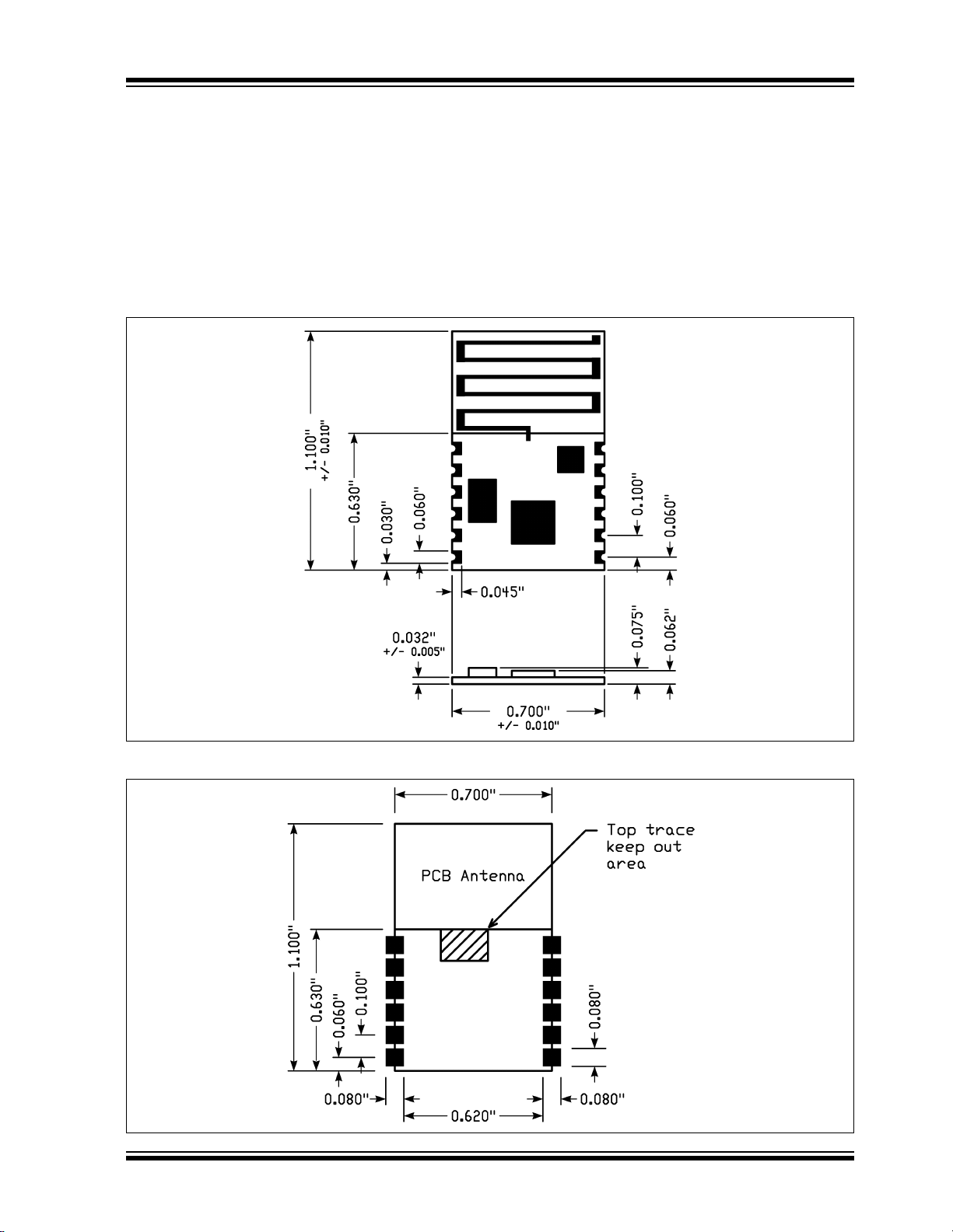
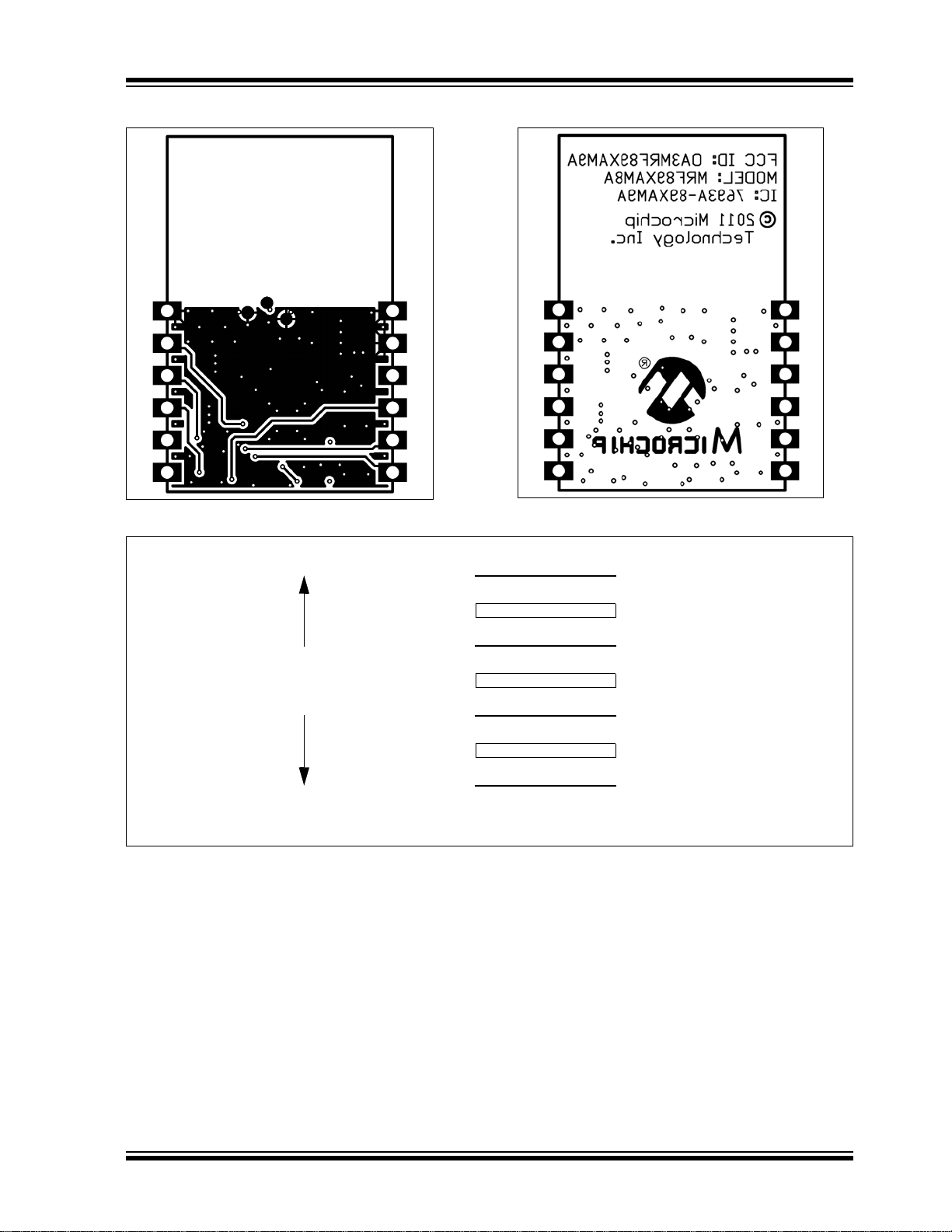
1.2 Mounting Details
The MRF89XAM9A is a surface mountable module.
Module dimensions are shown in Figure 1-3. The
module PCB is 0.032" thick with castellated mounting
holes on the edge. Figure 1-4 is the recommended host
PCB footprint for the MRF89XAM9A.
FIGURE 1-3: MODULE DETAILS
The MRF89XAM9A has an integrated PCB antenna.
For the best performance, follow the mounting details
shown in Figure 1-5. It is recommended that the
module be mounted on the edge of the host PCB and
an area around the antenna, approximately 3.4" (8.6
cm), be kept clear of metal objects for best
performance. A host PCB ground plane around the
MRF89XAM9A acts as a counterpoise to the PCB
antenna. It is recommended to extend the ground plane
at least 0.4" (1 cm) around the module.
FIGURE 1-4: RECOMMENDED PCB FOOTPRINT
© 2011 Microchip Technology Inc. Preliminary DS00000A-page 5
Page 8
MRF89XAM9A
3.4”
3.4”
0.4”
0.4”
Edge of PCB
0.470”
Keep area around antenna
(approximately 3.4 (6.8 cm)
inches) clear of metallic structures
for best performance
Host PCB Top Copper Ground
Plane (Antenna Counterpoise):
Extend the host PCB top copper
ground plane under and to the left
and right side of the module at least
0.4 inches (1 cm) for best antenna
performance.
FIGURE 1-5: MOUNTING DETAILS
DS00000A-page 6 Preliminary © 2011 Microchip Technology Inc.
Page 9

MRF89XAM9A
1.3 Operation
The MRF89XAM9A module is based on the Microchip
Technology MRF89XA Ultra Low-Power, Integrated
ISM Band Sub-GHz Transceiver IC. Data
communication and module configuration are
documented in the “MRF89XA Ultra Low-Power,
Integrated ISM Band Sub-GHz Transceiver Data
Sheet” (DS70622).
This section emphasizes operational settings that are
unique to the MRF89XAM9A module design that must
be followed for proper operation.
1.3.1 RESET
Pin 2 of the module, RESET, allows for an external
reset of the MRF89XA IC. RESET is connected to the
TEST8 pin of the MRF89XA IC. During normal
operations of the MRF89XAM9A, the RESET pin
should be held in a high impedance state. For more
information on Assertion of the RESET pin, refer to the
“Section 3.1.2 Manual Reset” of “MRF89XA Data
Sheet” (DS70622).
1.3.2 CRYSTAL FREQUENCY
When calculating frequency deviation, bit rate, receiver
bandwidth, and PLL R, P and S values, use crystal
frequency f
= 12.8 MHz.
xtal
1.3.3 CLOCK OUTPUT (CLKOUT)
The CLKOUT pin 19 of the MRF89XA IC is not used on
the module. Ensure that the CLKOUT signal is disabled
to minimize the current consumption.
1.3.4 FREQUENCY BAND SELECT
The Frequency Band Select (FBS<1:0>) bits in the
GCONREG<4:3> should be set for target channel
range 902–915 MHz FBS<1:0> = '00' or 915–928 MHz
FBS<1:0> = '01'.
1.3.5 VCO TANK TRIM VALUE
The VCO Trim (VCOT<1:0>) bits in the
GCONREG<2:1> should be set for VCOT<1:0> = '11'
for the inductor values of the module.
© 2011 Microchip Technology Inc. Preliminary DS00000A-page 7
Page 10

MRF89XAM9A
NOTES:
DS00000A-page 8 Preliminary © 2011 Microchip Technology Inc.
Page 11
MRF89XAM9A
Note 1
+
C2
1 0
μ
F
C1
0.1
μ
F
To Host
Microcontroller
To Host
Microcontroller
U1
MRF89XAM9A-I/RM
+ 3.3V
GND
RESET
CSCON
IRQ0
SDI
SCK
GND
GND
V
IN
IRQ1
CSDATA
SDO
1
2
3
4
5
6
12
11
10
9
8
7
Note: For battery powered applications, place a 10 μF capacitor in parallel with the 0.1 μF bypass
capacitor to provide a low impedance during startup sequences.
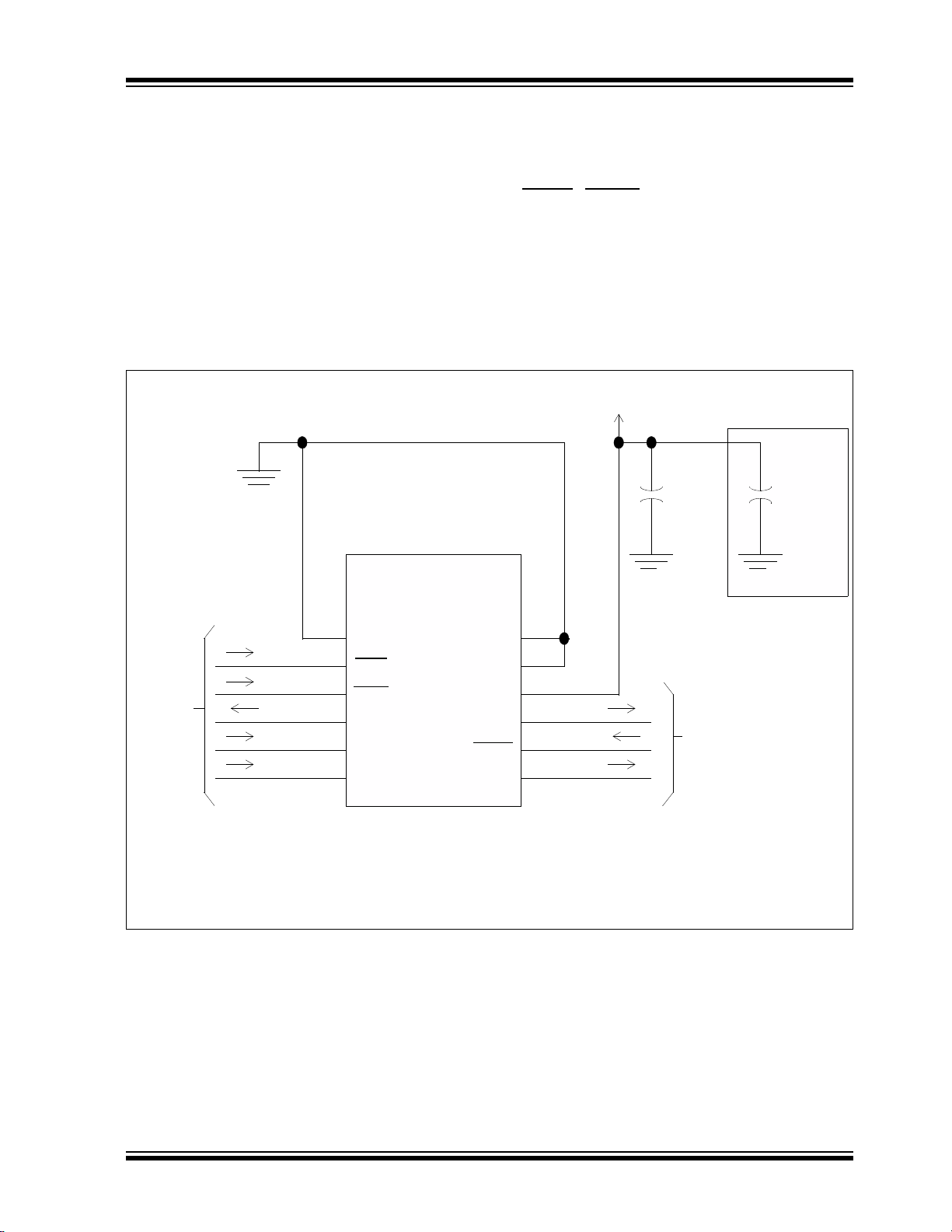
2.0 CIRCUIT DESCRIPTION
The MRF89XAM9A module interfaces to Microchip’s
PIC16, PIC 18, PIC24, dsPIC33 and PIC32
microcontrollers with a minimum of external
components through digital only connections. An
example application schematic is shown in Figure 2-2.
2.1 Module Schematic
The MRF89XAM9A module is based on the Microchip
Technology MRF89XA Ultra Low-Power, Integrated
ISM Band sub-GHz Transceiver IC. The serial I/O
(CSCON
IRQ0 and IRQ1 pins are brought out to the module
pins. Crystal X1 is a 12.8 MHz crystal with a
frequency tolerance of ±10 ppm at 25°C. The RFIO
output is matched to the SAW filter FL1 and further
matched to the PCB trace antenna.
Figure 2-2 illustrates the MRF89XAM9A schematics.
Table 2-1 details the Bill of Materials (BOM).
FIGURE 2-1: MRF89XAM9A APPLICATION SCHEMATIC
, CSDATA, SCK, SDO and SDI), RESET,
© 2011 Microchip Technology Inc. Preliminary DS00000A-page 9
Page 12

DS00000A-page 10 Preliminary © 2011 Microchip Technology Inc.
Note: Designators not used: C6, L5
FIGURE 2-2: MRF89XAM9A SCHEMATIC
MRF89XAM9A
Page 13

MRF89XAM9A
TABLE 2-1: MRF89XAM9A BILL OF MATERIALS
Desi
gnatorValue Description Manufacturer Part Number
C1 0.047 µF Capacitor, Ceramic, 10V, ±10%, X7R, SMT
0402
C2 0.22 µF Capacitor, Ceramic, 16V, ±10%, X7R, SMT
0402
C3 1 µF Capacitor, Ceramic, 6.3V, ±10%, X5R, SMT
0603
C4 30 pF Capacitor, Ceramic, 50V, ±5%, UHI-Q NP0,
SMT 0402
C5 1.8 pF Capacitor, Ceramic, 50V, ±0.1 pF, UHI-Q
NP0, SMT 0402
C6 — Designator not used — —
C7 33 pF Capacitor, Ceramic, 50V, ±5%, C0G, SMT
0402
C8 0.1 µF Capacitor, Ceramic, 16V, ±10%, X7R, SMT
0402
C9 680 pF Capacitor, Ceramic, 50V, ±5%, C0G, SMT
0402
C10 0.01 µF Capacitor, Ceramic, 16V, ±10%, X7R, SMT
0402
C11 1.0 pF Capacitor, Ceramic, 50V, ±0.1 pF, UHI-Q
NP0, SMT 0402
C12 0.9 pF Capacitor, Ceramic, 50V, ±0.1 pF, UHI-Q
NP0, SMT 0402
FL1 TA0281A Filter, SAW, 902–928 MHz Tai-saw Technology TA0281A
L1 10 nH Inductor, Ceramic, ±5%, SMT 0402 Johanson Technology L-07C10NJV6T
L2 100 nH Inductor, Ceramic, ±5%, SMT 0402 Johanson Technology L-07CR10JV6T
L3 5.6 nH Inductor, Wirewound, ±5%, SMT 0402 Johanson Technology L-07W5N6JV4T
L4 5.6 nH Inductor, Wirewound, ±5%, SMT 0402 Johanson Technology L-07W5N6JV4T
L5 — Designator not used — —
L6 10 nH Inductor, Ceramic, ±5%, SMT 0402 Johanson Technology L-07C10NJV6T
R1 1Ω Resistor, 1%, ±100 ppm/
R2 100KΩ Resistor, 5%, ±100 ppm/
R3 6.8KΩ Resistor, 1%, ±100 ppm/0C, SMT 0402 Yageo RC0402FR-076K8L
U1 MRF89XA Transceiver, Ultra Low-Power, Integrated
Sub-GHz
X1 12.8 MHz Crystal, ±10 ppm, 15 pF, ESR 100 ohms,
SMT 5 x 3.2mm
0
C, SMT 0402 Vishay/Dale CRCW04021R00FKED
0
C, SMT 0402 Yageo RC0402JR-07100KL
Murata GRM155R71A473KA01D
Murata GRM155R71C224KA12D
Murata GRM188R60J105KA01D
Johanson Technology 250R07S300JV4T
Johanson Technology 500R07S1R8BV4
Murata GRM1555C1H330JZ01D
Murata GRM155R71C104KA88D
Murata GRM1555C1H681JA01D
Murata GRM155R71C103KA01D
Johanson Technology 500R07S1R0BV4
Johanson Technology 500R07S0R9BV4
Microchip Technology MRF89XA-I/MQ
Abracon ABM3B-155-12.800MHz-T
© 2011 Microchip Technology Inc. Preliminary DS00000A-page 11
Page 14
MRF89XAM9A
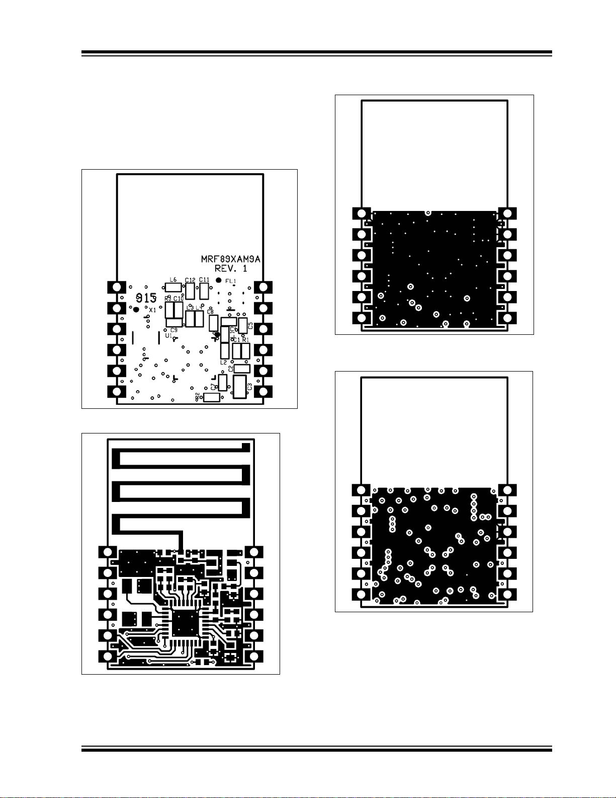
2.2 Printed Circuit Board
The MRF89XAM9A module PCB is constructed with
high temperature FR4 material, four layers and 0.032
inches thick. The layers are shown in Figure 2-3
through Figure 2-8. The stack up of the PCB is shown
in Figure 2-9
FIGURE 2-3: TOP SILK SCREEN
FIGURE 2-5: LAYER 2 — GROUND
PLANE
FIGURE 2-6: LAYER 3 — POWER
PLANE
FIGURE 2-4: TOP COPPER
© 2011 Microchip Technology Inc. Preliminary DS00000A-page 12
Page 15
MRF89XAM9A
Top Copper
Ground Plane
Power Plane
Bottom Copper
1/2 oz. Copper
1/2 oz. Copper
1/2 oz. Copper
1/2 oz. Copper
8 mil FR4
12 mil FR4
8 mil FR4
0.032”
±0.005”
FIGURE 2-7: BOTTOM COPPER FIGURE 2-8: BOTTOM SILK SCREEN
FIGURE 2-9: PCB LAYER STACK UP
© 2011 Microchip Technology Inc. Preliminary DS00000A-page 13
Page 16
MRF89XAM9A
16.8mm
1.0mm
8.4mm
1.1mm
0.5mm
2.5mm
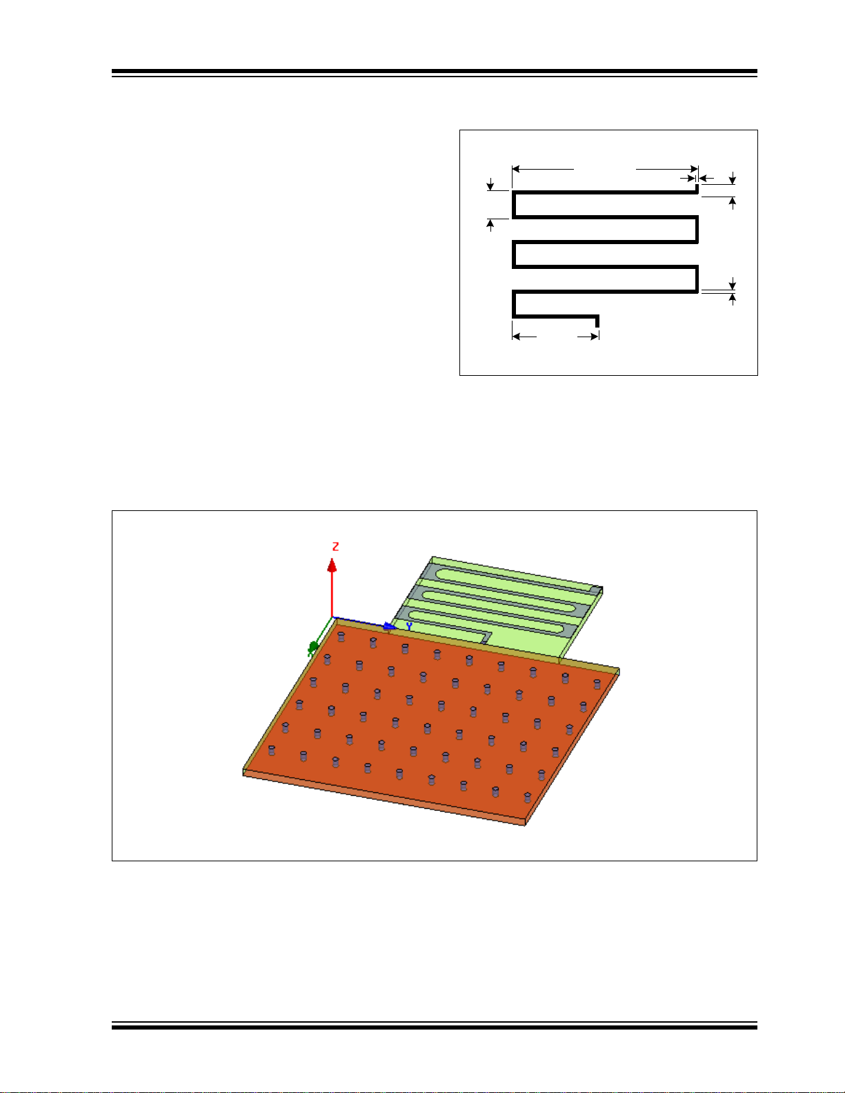
2.3 PCB Antenna
The PCB antenna is fabricated on the top copper trace.
Figure 2-11 shows the trace dimensions. The layers
below the antenna have no copper traces. The ground
and power planes under the components serve as a
counterpoise to the PCB antenna. Additional ground
plane on the host PCB will substantially enhance the
performance of the module. For best performance,
place the module on the host PCB by following the
recommendations in Section 1.2, Mounting Details.
The PCB antenna was designed and simulated using
Ansoft Designer
software by ANSYS, Inc. (www.ansoft.com). The
design goal was to create a compact, low-cost antenna
with the best radiation pattern. Figure 2-11 shows the
simulation drawing and Figure 2-12 and Figure 2-13
show the 2D and 3D radiation patterns, respectively. As
shown by the radiation patterns, the performance of the
antenna is dependant upon the orientation of the
module. Figure 2-14 shows the impedance simulation
and Figure 2-15 shows the actual impedance
measurement. The discrete matching circuitry matches
the impedance of the antenna with the SAW filter and
MRF89XA transceiver IC.
®
and HFSS™ 3D full-wave solver
FIGURE 2-10: PCB ANTENNA
FIGURE 2-11: PCB ANTENNA SIMULATION DRAWING
DIMENSIONS
© 2011 Microchip Technology Inc. Preliminary DS00000A-page 14
Page 17

FIGURE 2-12: SIMULATED 2D RADIATION PATTERN
MRF89XAM9A
FIGURE 2-13: SIMULATED 3D RADIATION PATTERN
© 2011 Microchip Technology Inc. Preliminary DS00000A-page 15
Page 18

FIGURE 2-14: SIMULATED PCB ANTENNA IMPEDANCE
MRF89XAM9A
FIGURE 2-15: SIMULATED PCB ANTENNA VSWR
© 2011 Microchip Technology Inc. Preliminary DS00000A-page 16
Page 19

3.0 REGULATORY APPROVAL
The MRF89XAM9A module has received regulatory
approvals for modular devices in the United States and
Canada. Modular approval allows the end user to place
the MRF89XAM9A module inside a finished product
and not require regulatory testing for an intentional
radiator (RF transmitter), provided no changes or
modifications are made to the module circuitry.
Changes or modifications could void the user’s
authority to operate the equipment. The end user must
comply with all of the instructions provided by the
Grantee, which indicate installation and/or operating
conditions necessary for compliance.
The integrator is still responsible for testing the end
product for any additional compliance requirements
required with this module installed (digital device
emission, PC peripheral requirements, etc.) in the
specific country that the end device will be marketed.
For more information on details on regulatory
compliance, refer to the specific country radio
regulations in the following sections.
3.1 United States
The MRF89XAM9A has received Federal
Communications Commission (FCC) CFR47
Telecommunications, Part 15 Subpart C “Intentional
Radiators” 15.247 and 15.249 and modular approval in
accordance with FCC Public Notice DA 00-1407
Released: June 26, 2000, Part 15 Unlicensed Modular
Transmitter Approval. The MRF89XAM9A module can
be integrated into a finished product without obtaining
subsequent and separate FCC certification.
The MRF89XAM9A module has been labeled with its
own FCC ID number, and if the FCC ID is not visible
when the module is installed inside another device,
then the outside of the finished product into which the
module is installed must also display a label referring
to the enclosed module. This exterior label can use
wording as following:
Contains Transmitter Module FCC ID:
9
OA3MRF8
-or-
Contains FCC ID: OA3MRF89XAM9A
This device complies with Part 15 of the FCC Rules.
Operation is subject to the following two conditions:
(1) this device may not cause harmful interference,
and (2) this device must accept any interference
received, including interference that may cause
undesired operation.
XAM9A
MRF89XAM9A
Requirements for product labeling are given in Part
15.19 Labelling Requirements.
The user’s manual should include the following
statement:
This equipment has been tested and found to comply
with the limits for a Class B digital device, pursuant to
part 15 of the FCC Rules. These limits are designed to
provide reasonable protection against harmful
interference in a residential installation. This
equipment generates, uses and can radiate radio
frequency energy, and if not installed and used in
accordance with the instructions, may cause harmful
interference to radio communications. However, there
is no guarantee that interference will not occur in a
particular installation. If this equipment does cause
harmful interference to radio or television reception,
which can be determined by turning the equipment
OFF and ON, the user is encouraged to try to correct
the interference by one or more of the following
measures:
• Reorient or relocate the receiving antenna.
• Increase the separation between the equipment
and receiver.
• Connect the equipment into an outlet on a
circuit different from that to which the receiver is
connected.
• Consult the dealer or an experienced radio/TV
technician for help.
3.1.1 MRF89XAM9A SETTINGS
To meet the FCC requirements, the following settings
must be observed by the integrator:
3.1.1.1 FSK Modulation
The following settings configure the MRF89XAM9A for
wideband digital modulation techniques that conform to
the requirements of Part 15.247. These settings allow
for higher radio frequency (RF) output power and
greater link budget:
• Bit Rate Setting: 50 - 200 kbps
- Transmit Power Maximum Setting:13 dBm
• Bit Rate Setting: 2 - 40 kbps
- Transmit Power Maximum Setting:7 dBm
• Frequency Deviation Setting: 200 kHz
• Data Whitening: On
• Transmit Bandwidth Setting: 400 kHz
• Lower Frequency Setting: 902.800 MHz
• Upper Frequency Setting: 926.500 MHz
© 2011 Microchip Technology Inc. Preliminary DS00000A-page 17
Page 20

MRF89XAM9A
3.1.1.2 OOK Modulation
The following settings configure the MRF89XAM9A for
narrowband operation that conform to the requirements
of Part 15.249. Part 15.249 requires a much lower
power setting than is allowed in Part 15.247. These settings are good for applications that require lower transmit power current consumption and shorter transmit
distances:
• Transmit Power Maximum Setting:1 dBm
• Bit Rate Maximum Setting: 16 kbps
• Frequency Deviation Setting: 200 kHz
• Transmit Bandwidth Setting: 400 kHz
• Lower Frequency Setting: 902.330 MHz
• Upper Frequency Setting: 927.500 MHz
3.1.2 RF EXPOSURE
All transmitters regulated by FCC must comply with RF
exposure requirements. OET Bulletin 65 “Evaluating
Compliance with FCC Guidelines for Human Exposure
to Radio Frequency Electromagnetic Fields” provides
assistance in determining whether proposed or existing
transmitting facilities, operations or devices comply
with limits for human exposure to RF fields adopted by
the Federal Communications Commission (FCC). The
bulletin offers guidelines and suggestions for
evaluating compliance.
If appropriate, compliance with exposure guidelines for
mobile and unlicensed devices can be accomplished
by the use of warning labels and by providing users
with information concerning minimum separation
distances from transmitting structures and proper
installation of antennas.
The following statement must be included as a
CAUTION statement in manuals and OEM products to
alert users of FCC RF Exposure compliance:
To satisfy FCC RF Exposure requirements for mobile
and base station transmission devices, a separation
distance of 20 cm or more should be maintained
between the antenna of this device and persons
during operation. To ensure compliance, operation at
closer than this distance is not recommended.
The antenna(s) used for this transmitter must not be
co-located or operating in conjunction with any other
antenna or transmitter.
If the MRF89XAM9A module is used in a portable
application (antenna is less than 20 cm from persons
during operation), the integrator is responsible for
performing Specific Absorption Rate (SAR) testing in
accordance with FCC rules 2.1091.
3.1.3 HELPFUL WEB SITES
Federal Communications Commission (FCC) http://
www.fcc.gov
DS00000A-page 18 Preliminary © 2011 Microchip Technology Inc.
Page 21

MRF89XAM9A
3.2 Canada
The MRF89XAM9A module has been certified for use in
Canada under Industry Canada (IC) Radio Standards
Specification (RSS) RSS-210 and RSS-Gen. Modular
approval permits the installation of a module in a host
device without the need to recertify the device.
Labeling Requirements for the Host Device (from
Section 3.2.1, RSS-Gen, Issue 3, December 2010):
The host device shall be properly labeled to identify the
module within the host device.
The Industry Canada certification label of a module
shall be clearly visible at all times when installed in the
host device, otherwise the host device must be labeled
to display the Industry Canada certification number of
the module, preceded by the words “Contains
transmitter module”, or the word “Contains”, or similar
wording expressing the same meaning, as follows:
Contains transmitter module IC: 7693A-89XAM9A
User Manual Notice for License-Exempt Radio
Apparatus (from Section 7.1.3 RSS-Gen, Issue 3,
December 2010):
User manuals for license-exempt radio apparatus shall
contain the following or equivalent notice in a
conspicuous location in the user manual or
alternatively on the device or both.
This device complies with Industry Canada licenseexempt RSS standard(s). Operation is subject to the
following two conditions: (1) this device may not
cause interference, and (2) this device must accept
any interference, including interference that may
cause undesired operation of the device.
Le présent appareil est conforme aux CNR
d'Industrie Canada applicables aux appareils radio
exempts de licence. L'exploitation est autorisée aux
deux conditions suivantes: (1) l'appareil ne doit pas
produire de brouillage, et (2) l'utilisateur de l'appareil
doit accepter tout brouillage radioélectrique subi,
même si le brouillage est susceptible d'en
compromettre le fonctionnement.
3.2.1 MRF89XAM9A SETTINGS
To meet Industry Canada (IC) requirements, the
following settings must be observed by the integrator:
3.2.1.1 FSK Modulation
The following settings configure the MRF89XAM9A for
wideband digital modulation techniques that conform to
the requirements of RSS-210 Issue 8 Annex 8. These
settings allow for higher radio frequency (RF) output
power and greater link budget.
• Bit Rate Setting: 50 - 200 kbps
- Transmit Power Maximum Setting:13 dBm
• Bit Rate Setting: 2 - 40 kbps
- Transmit Power Maximum Setting:7 dBm
• Frequency Deviation Setting: 200 kHz
• Data Whitening: On
• Transmit Bandwidth Setting: 400 kHz
• Lower Frequency Setting: 902.800 MHz
• Upper Frequency Setting: 926.500 MHz
3.2.1.2 OOK Modulation
The following settings configure the MRF89XAM9A for
narrowband operation that conform to the requirements
of RSS-Gen Issue 3. RSS-Gen Issue 3 requires a
much lower power setting than is allowed in Part RSS210 Issue 8 Annex 8. These settings are good for
applications that require lower transmit power current
consumption and shorter transmit distances.
• Transmit Power Maximum Setting:1 dBm
• Bit Rate Maximum Setting: 16 kbps
• Frequency Deviation Setting: 200 kHz
• Transmit Bandwidth Setting: 400 kHz
• Lower Frequency Setting: 902.330 MHz
• Upper Frequency Setting: 927.500 MHz
3.2.2 HELPFUL WEB SITES
Industry Canada: http://www.ic.gc.ca/
© 2011 Microchip Technology Inc. Preliminary DS00000A-page 19
Page 22

MRF89XAM9A
NOTES:
DS00000A-page 20 Preliminary © 2011 Microchip Technology Inc.
Page 23

MRF89XAM9A
4.0 ELECTRICAL CHARACTERISTICS
Absolute Maximum Ratings
Ambient temperature under bias.............................................................................................................. -40°C to +85°C
Storage temperature .............................................................................................................................. -55°C to +125°C
Voltage on V
Voltage on any combined digital and analog pin with respect to V
Input current into pin (except V
Electrostatic discharge with human body model.................................................................................................... 1000V
NOTICE: Stresses above those listed under “Absolute Maximum Ratings” may cause permanent damage to the
device. This is a stress rating only and functional operation of the device at those or any other conditions above
those indicated in the operation listings of this specification is not implied. Exposure to maximum rating conditions for
extended periods may affect device reliability.
IN with respect to VSS ................................................................................................................ -0.3V to 6V
SS (except VIN) ...........................-0.3V to (VIN + 0.3V)
IN and VSS)........................................................................................... -25 mA to 25 mA
© 2011 Microchip Technology Inc. Preliminary DS00000A-page 21
Page 24

MRF89XAM9A
TABLE 4-1: RECOMMENDED OPERATING CONDITIONS
Parameter Min Typ Max Unit Condition
Ambient Operating Temperature -40 — +85 °C —
Supply Voltage for RF, Analog and Digital Circuits 2.1 — 3.6 V —
Supply Voltage for Digital I/O 2.1 — 3.6 V —
Input High Voltage (V
Input Low Voltage (VIL) -0.3V — 0.2 * VIN V—
AC Peak Voltage on Open Collector Outputs (IO)
Note 1: At minimum, V
TABLE 4-2: CURRENT CONSUMPTION
Symbol Chip Mode Min Typ Max Unit Condition
I
DDSL Sleep — 0.1 2 µA Sleep clock disabled, all blocks
I
DDST Idle — 65 80 µA Oscillator and baseband enabled
IDDFS Frequency Synthesizer — 1.3 1.7 mA Frequency synthesizer running
I
DDTX Tx —
IDDRX Rx — 3.0 3.5 mA —
Note 1: Guaranteed by design and characterization.
IH) 0.5 * VIN —VIN + 0.3 V —
(1)
VIN – 1.5 — VIN + 1.5 V —
IN – 1.5V should not be lower than 1.8V.
disabled
—
25
16
30
21
mA
mA
Output power = +10 dBm
Output power = +1 dBm
(1)
TABLE 4-3: DIGITAL I/O PIN INPUT SPECIFICATIONS
(1)
Symbol Characteristic Min Typ Max Unit Condition
IL Input Low Voltage — — 0.2 * VIN V—
V
V
IH Input High Voltage 0.8 * VIN —— V —
IIL Input Low Leakage Current
I
IH Input High Leakage Current -0.5 — 0.5 µA VIH = VIN, VIN = 3.7
V
OL Digital Low Output Voltage — — 0.1 * VIN —IOL = 1 mA
V
OH Digital Low Output 0.9 * VIN —— V IOH = -1 mA
Note 1: Measurement Conditions: T
(2)
-0.5 — 0.5 µA VIL = 0V
A = 25°C, VIN = 3.3V, Crystal Frequency = 12.8 MHz, unless otherwise
specified.
2: Negative current is defined as the current sourced by the pin.
DS00000A-page 22 Preliminary © 2011 Microchip Technology Inc.
Page 25

MRF89XAM9A
TABLE 4-4: PLL PARAMETERS AC CHARACTERISTICS
Symbol Parameter Min Typ Max Unit Condition
FRO Frequency Ranges 902 — 928 MHz —
BRFSK Bit Rate (FSK) 1.56 — 40 kbps NRZ
BROOK Bit Rate (OOK) 1.56 — 16 kbps NRZ
FDFSK Frequency Deviation (FSK) 33 50 200 kHz —
FXTAL Crystal Oscillator Frequency 9 12.8 — MHz —
FSSTP Frequency Synthesizer Step — 2 — kHz Variable, depending on the
TSOSC Oscillator Wake-up Time — 1.5 5 ms From Sleep mode
TSFS Frequency Synthesizer Wake-
up Time; at most, 10 kHz
away from the target
TSHOP Frequency Synthesizer Hop
Time; at most, 10 kHz away
from the target
Note 1: Guaranteed by design and characterization.
— 500 800 µs From Stand-by mode
— 180 — µs 200 kHz step
— 200 — µs 1 MHz step
— 250 — µs 5 MHz step
— 260 — µs 7 MHz step
— 290 — µs 12 MHz step
— 320 — µs 20 MHz step
— 340 — µs 27 MHz step
(1)
frequency
(1)
© 2011 Microchip Technology Inc. Preliminary DS00000A-page 23
Page 26

MRF89XAM9A
TABLE 4-5: RECEIVER AC CHARACTERISTICS
(1)
Symbol Parameter Min Typ Max Unit Condition
RSF Sensitivity (FSK) — -107 — dBm 915 MHz, BR = 25 kbps,
= 50 kHz, f
f
dev
= 100 kHz
c
— -103 — dBm 915 MHz, BR = 66.7 kbps,
f
= 100 kHz, f
dev
= 200 kHz
c
RSO Sensitivity (OOK) — -113 — dBm 915 MHz, 2 kbps NRZ
fc – fo = 50 kHz, f
= 50 kHz
o
— -106 — dBm 915 MHz, 16.7 kbps NRZ
fc – fo = 100 kHz, f
= 100 kHz
o
CCR Co-Channel Rejection — -12 — dBc Modulation as wanted signal
ACR Adjacent Channel Rejection — 27 — dB Offset = 300 kHz, unwanted tone is
not modulated
— 52 — dB Offset = 600 kHz, unwanted tone is
not modulated
— 57 — dB Offset = 1.2 MHz, unwanted tone is
not modulated
BI Blocking Immunity — -48 — dBm Offset = 1 MHz, unmodulated
— -37 — dBm Offset = 2 MHz, unmodulated, no
SAW
— -33 — dBm Offset = 10 MHz, unmodulated, no
SAW
RXBWF Receiver Bandwidth in FSK
RXBWU Receiver Bandwidth in OOK
Mode
Mode
(2)
(2)
ITP3 Input Third Order Intercept
Point
50 — 250 kHz Single side BW, Polyphase Off
50 — 400 kHz Single side BW, Polyphase On
— -28 — dBm Interferers at 1 MHz and 1.950 MHz
offset
TSRWF Receiver Wake-up Time — 280 500 µs From FS to Rx ready
TSRWS Receiver Wake-up Time — 600 900 µs From Stand-by to Rx ready
TSRHOP Receiver Hop Time from Rx
Ready to Rx Ready with a
Frequency Hop
— 400 — µs 200 kHz step
— 400 — µs 1 MHz step
— 460 — µs 5 MHz step
— 480 — µs 7 MHz step
— 520 — µs 12 MHz step
— 550 — µs 20 MHz step
— 600 — µs 27 MHz step
RSSIST RSSI Sampling Time — — 1/f
dev
s From Rx ready
RSSTDR RSSI Dynamic Range — 70 — dB Ranging from sensitivity
Note 1: Guaranteed by design and characterization.
2: This reflects the whole receiver bandwidth, as described by conditions for active and passive filters.
DS00000A-page 24 Preliminary © 2011 Microchip Technology Inc.
Page 27

MRF89XAM9A
TABLE 4-6: TRANSMITTER AC CHARACTERISTICS
Symbol Description Min Typ Max Unit Condition
RFOP RF Output Power, Programmable
with 8 Steps of typ. 3 dB
PN Phase Noise — -112 — dBc/Hz Measured with a 600 kHz
TXSP Transmitted Spurious — — -47 dBc At any offset between 200 kHz
Tx2 Second Harmonic
Tx3 Third Harmonic
Tx4 Fourth Harmonic
Txn Harmonics above Tx4
FSKDEV FSK Deviation ±33 ±55 ±200 kHz Programmable
TSTWF Transmitter Wake-up Time — 120 500 µs From FS to Tx ready
TSTWS Transmitter Wake-up Time — 600 900 µs From Stand-by to Tx ready
Note 1: Guaranteed by design and characterization.
2: Transmitter in-circuit performance with SAW filter and crystal.
— +12.5 — dBm Maximum power setting
— -8.5 — dBm Minimum power setting
——-40dBm
(1)
offset at the transmitter output
and 600 kHz, unmodulated
carrier, f
No modulation, see Note
= 50 kHz
dev
(2)
4.1 Timing Specification and Diagram
TABLE 4-7: SPI TIMING SPECIFICATION
Parameter Min Typ Max Unit Condition
SPI Configure Clock Frequency — — 6 MHz —
SPI Data Clock Frequency — — 1 MHz —
Data Hold and Setup Time 2 — — µs —
SDI Setup Time for SPI Configure 250 — — ns —
SDI Setup Time for SPI Data 312 — — ns —
CSCON
SCK Falling Edge to CSCON High
CSDATA
SCK Falling Edge to CSDATA
CSCON
CSDATA
Note 1: Typical Values: T
Low to SCK Rising Edge;
Low to SCK Rising Edge;
High
Rising to Falling Edge 500 — — ns —
Rising to Falling Edge 625 — — ns —
A = 25°C, VIN = 3.3V, Crystal Frequency = 12.8 MHz, unless otherwise specified.
2: Negative current is defined as the current sourced by the pin.
500 — — ns —
625 — — ns —
(1,2)
© 2011 Microchip Technology Inc. Preliminary DS00000A-page 25
Page 28

MRF89XAM9A
NOTES:
DS00000A-page 26 Preliminary © 2011 Microchip Technology Inc.
Page 29

APPENDIX A: REVISION HISTORY
Revision A (May 2011)
This is the Initial release of the document.
MRF89XAM9A
© 2011 Microchip Technology Inc. Preliminary DS00000A-page 27
Page 30

MRF89XAM9A
NOTES:
DS00000A-page 28 Preliminary © 2011 Microchip Technology Inc.
Page 31

MRF89XAM9A
THE MICROCHIP WEB SITE
Microchip provides online support via our WWW site at
www.microchip.com. This web site is used as a means
to make files and information easily available to
customers. Accessible by using your favorite Internet
browser, the web site contains the following
information:
• Product Support – Data sheets and errata,
application notes and sample programs, design
resources, user’s guides and hardware support
documents, latest software releases and archived
software
• General Technical Support – Frequently Asked
Questions (FAQ), technical support requests,
online discussion groups, Microchip consultant
program member listing
• Business of Microchip – Product selector and
ordering guides, latest Microchip press releases,
listing of seminars and events, listings of
Microchip sales offices, distributors and factory
representatives
CUSTOMER CHANGE NOTIFICATION SERVICE
CUSTOMER SUPPORT
Users of Microchip products can receive assistance
through several channels:
• Distributor or Representative
• Local Sales Office
• Field Application Engineer (FAE)
• Technical Support
• Development Systems Information Line
Customers should contact their distributor,
representative or field application engineer (FAE) for
support. Local sales offices are also available to help
customers. A listing of sales offices and locations is
included in the back of this document.
T echnical support is available through the web site
at: http://microchip.com/support
Microchip’s customer notification service helps keep
customers current on Microchip products. Subscribers
will receive e-mail notification whenever there are
changes, updates, revisions or errata related to a
specified product family or development tool of interest.
To register, access the Microchip web site at
www.microchip.com. Under “Support”, click on
“Customer Change Notification” and follow the
registration instructions.
© 2011 Microchip Technology Inc. Preliminary DS00000A-page 29
Page 32

MRF89XAM9A
TO: Technical Publications Manager
RE: Reader Response
Total Pages Sent ________
From:
Name
Company
Address
City / State / ZIP / Country
Telephone: (_______) _________ - _________
Application (optional):
Would you like a reply? Y N
Device: Literature Number:
Questions:
FAX: (______) _________ - _________
DS00000AMRF89XAM9A
READER RESPONSE
It is our intention to provide you with the best documentation possible to ensure successful use of your Microchip
product. If you wish to provide your comments on organization, clarity, subject matter, and ways in which our
documentation can better serve you, please FAX your comments to the Technical Publications Manager at
(480) 792-4150.
Please list the following information, and use this outline to provide us with your comments about this document.
1. What are the best features of this document?
2. How does this document meet your hardware and software development needs?
3. Do you find the organization of this document easy to follow? If not, why?
4. What additions to the document do you think would enhance the structure and subject?
5. What deletions from the document could be made without affecting the overall usefulness?
6. Is there any incorrect or misleading information (what and where)?
7. How would you improve this document?
DS00000A-page 30 Preliminary © 2011 Microchip Technology Inc.
Page 33

MRF89XAM9A
Device MRF89XAM9A-I/RM: Ultra Low-Power, Integrated ISM Band Sub-GHz
Transceiver module
Temperature
Range
I = -40ºC to +85ºC (Industrial)
Example:
a) MRF89XAM9A-I/RM: Industrial temperature
tray.
b) MRF89XAM9AT-I/RM: Industrial temperature
tape and reel,
PART NO
Device
M
Module
X
Module
Type
Tape and
Reel
-X
Temperature
Range
T
PRODUCT IDENTIFICATION SYSTEM
To order or obtain information, for example, on pricing or delivery, refer to the factory or the listed sales office.
© 2011 Microchip Technology Inc. Preliminary DS00000A-page 31
Page 34

Worldwide Sales and Service
AMERICAS
Corporate Office
2355 West Chandler Blvd.
Chandler, AZ 85224-6199
Tel: 480-792-7200
Fax: 480-792-7277
Technical Support:
http://www.microchip.com/
support
Web Address:
www.microchip.com
Atlanta
Duluth, GA
Tel: 678-957-9614
Fax: 678-957-1455
Boston
Westborough, MA
Tel: 774-760-0087
Fax: 774-760-0088
Chicago
Itasca, IL
Tel: 630-285-0071
Fax: 630-285-0075
Cleveland
Independence, OH
Tel: 216-447-0464
Fax: 216-447-0643
Dallas
Addison, TX
Tel: 972-818-7423
Fax: 972-818-2924
Detroit
Farmington Hills, MI
Tel: 248-538-2250
Fax: 248-538-2260
Indianapolis
Noblesville, IN
Tel: 317-773-8323
Fax: 317-773-5453
Los Angeles
Mission Viejo, CA
Tel: 949-462-9523
Fax: 949-462-9608
Santa Clara
Santa Clara, CA
Tel: 408-961-6444
Fax: 408-961-6445
Toronto
Mississauga, Ontario,
Canada
Tel: 905-673-0699
Fax: 905-673-6509
ASIA/PACIFIC
Asia Pacific Office
Suites 3707-14, 37th Floor
Tower 6, The Gateway
Harbour City, Kowloon
Hong Kong
Tel: 852-2401-1200
Fax: 852-2401-3431
Australia - Sydney
Tel: 61-2-9868-6733
Fax: 61-2-9868-6755
China - Beijing
Tel: 86-10-8528-2100
Fax: 86-10-8528-2104
China - Chengdu
Tel: 86-28-8665-5511
Fax: 86-28-8665-7889
China - Chongqing
Tel: 86-23-8980-9588
Fax: 86-23-8980-9500
China - Hong Kong SAR
Tel: 852-2401-1200
Fax: 852-2401-3431
China - Nanjing
Tel: 86-25-8473-2460
Fax: 86-25-8473-2470
China - Qingdao
Tel: 86-532-8502-7355
Fax: 86-532-8502-7205
China - Shanghai
Tel: 86-21-5407-5533
Fax: 86-21-5407-5066
China - Shenyang
Tel: 86-24-2334-2829
Fax: 86-24-2334-2393
China - Shenzhen
Tel: 86-755-8203-2660
Fax: 86-755-8203-1760
China - Wuhan
Tel: 86-27-5980-5300
Fax: 86-27-5980-5118
China - Xian
Tel: 86-29-8833-7252
Fax: 86-29-8833-7256
China - Xiamen
Tel: 86-592-2388138
Fax: 86-592-2388130
China - Zhuhai
Tel: 86-756-3210040
Fax: 86-756-3210049
ASIA/PACIFIC
India - Bangalore
Tel: 91-80-3090-4444
Fax: 91-80-3090-4123
India - New Delhi
Tel: 91-11-4160-8631
Fax: 91-11-4160-8632
India - Pune
Tel: 91-20-2566-1512
Fax: 91-20-2566-1513
Japan - Yokohama
Tel: 81-45-471- 6166
Fax: 81-45-471-6122
Korea - Daegu
Tel: 82-53-744-4301
Fax: 82-53-744-4302
Korea - Seoul
Tel: 82-2-554-7200
Fax: 82-2-558-5932 or
82-2-558-5934
Malaysia - Kuala Lumpur
Tel: 60-3-6201-9857
Fax: 60-3-6201-9859
Malaysia - Penang
Tel: 60-4-227-8870
Fax: 60-4-227-4068
Philippines - Manila
Tel: 63-2-634-9065
Fax: 63-2-634-9069
Singapore
Tel: 65-6334-8870
Fax: 65-6334-8850
Taiwan - Hsin Chu
Tel: 886-3-6578-300
Fax: 886-3-6578-370
Taiwan - Kaohsiung
Tel: 886-7-213-7830
Fax: 886-7-330-9305
Taiwan - Taipei
Tel: 886-2-2500-6610
Fax: 886-2-2508-0102
Thailand - Bangkok
Tel: 66-2-694-1351
Fax: 66-2-694-1350
EUROPE
Austria - Wels
Tel: 43-7242-2244-39
Fax: 43-7242-2244-393
Denmark - Copenhagen
Tel: 45-4450-2828
Fax: 45-4485-2829
France - Paris
Tel: 33-1-69-53-63-20
Fax: 33-1-69-30-90-79
Germany - Munich
Tel: 49-89-627-144-0
Fax: 49-89-627-144-44
Italy - Milan
Tel: 39-0331-742611
Fax: 39-0331-466781
Netherlands - Drunen
Tel: 31-416-690399
Fax: 31-416-690340
Spain - Madrid
Tel: 34-91-708-08-90
Fax: 34-91-708-08-91
UK - Wokingham
Tel: 44-118-921-5869
Fax: 44-118-921-5820
02/18/11
DS00000A-page 32 © 2011 Microchip Technology Inc.
 Loading...