

Page 1

MCP6V01
Input Offset
Demo Board
User’s Guide
© 2009 Microchip Technology Inc. DS51801A
Page 2

Note the following details of the code protection feature on Microchip devices:
• Microchip products meet the specification contained in their particular Microchip Data Sheet.
• Microchip believes that its family of products is one of the most secure families of its kind on the market today, when used in the
intended manner and under normal conditions.
• There are dishonest and possibly illegal methods used to breach the code protection feature. All of these methods, to our
knowledge, require using the Microchip products in a manner outside the operating specifications contained in Microchip’s Data
Sheets. Most likely, the person doing so is engaged in theft of intellectual property.
• Microchip is willing to work with the customer who is concerned about the integrity of their code.
• Neither Microchip nor any other semiconductor manufacturer can guarantee the security of their code. Code protection does not
mean that we are guaranteeing the product as “unbreakable.”
Code protection is constantly evolving. We at Microchip are committed to continuously improving the code protection features of our
products. Attempts to break Microchip’s code protection feature may be a violation of the Digital Millennium Copyright Act. If such acts
allow unauthorized access to your software or other copyrighted work, you may have a right to sue for relief under that Act.
Information contained in this publication regarding device
applications and the like is provided only for your convenience
and may be superseded by updates. It is your responsibility to
ensure that your application meets with your specifications.
MICROCHIP MAKES NO REPRESENTATIONS OR
WARRANTIES OF ANY KIND WHETHER EXPRESS OR
IMPLIED, WRITTEN OR ORAL, STATUTORY OR
OTHERWISE, RELATED TO THE INFORMATION,
INCLUDING BUT NOT LIMITED TO ITS CONDITION,
QUALITY, PERFORMANCE, MERCHANTABILITY OR
FITNESS FOR PURPOSE. Microchip disclaims all liability
arising from this information and its use. Use of Microchip
devices in life support and/or safety applications is entirely at
the buyer’s risk, and the buyer agrees to defend, indemnify and
hold harmless Microchip from any and all damages, claims,
suits, or expenses resulting from such use. No licenses are
conveyed, implicitly or otherwise, under any Microchip
intellectual property rights.
Trademarks
The Microchip name and logo, the Microchip logo, Accuron,
dsPIC, K
EELOQ, KEELOQ logo, MPLAB, PIC, PICmicro,
PICSTART, rfPIC, SmartShunt and UNI/O are registered
trademarks of Microchip Technology Incorporated in the
U.S.A. and other countries.
FilterLab, Linear Active Thermistor, MXDEV, MXLAB,
SEEVAL, SmartSensor and The Embedded Control Solutions
Company are registered trademarks of Microchip Technology
Incorporated in the U.S.A.
Analog-for-the-Digital Age, Application Maestro, CodeGuard,
dsPICDEM, dsPICDEM.net, dsPICworks, dsSPEAK, ECAN,
ECONOMONITOR, FanSense, In-Circuit Serial
Programming, ICSP, ICEPIC, Mindi, MiWi, MPASM, MPLAB
Certified logo, MPLIB, MPLINK, mTouch, PICkit, PICDEM,
PICDEM.net, PICtail, PIC
32
logo, PowerCal, PowerInfo,
PowerMate, PowerT ool, REAL ICE, rfLAB, Select Mode, Total
Endurance, WiperLock and ZENA are trademarks of
Microchip Technology Incorporated in the U.S.A. and other
countries.
SQTP is a service mark of Microchip Technology Incorporated
in the U.S.A.
All other trademarks mentioned herein are property of their
respective companies.
© 2009, Microchip Technology Incorporated, Printed in the
U.S.A., All Rights Reserved.
Printed on recycled paper.
Microchip received ISO/TS-16949:2002 certification for its worldwide
headquarters, design and wafer fabrication facilities in Chandler and
T empe, Arizona; Gresham, Oregon and design centers in California
and India. The Company’s quality system processes and procedures
are for its PIC
devices, Serial EEPROMs, microperipherals, nonvolatile memo ry and
analog products. In addition, Microchip’s quality system for the desig n
and manufacture of development systems is ISO 9001:2000 certified.
®
MCUs and dsPIC® DSCs, KEELOQ
®
code hopping
DS51801A-page ii © 2009 Microchip Technology Inc.
Page 3

MCP6V01 INPUT OFFSET
DEMO BOARD USER’S GUIDE
Table of Contents
Preface ...........................................................................................................................1
Introduction............................................................................................................1
Document Layout..................................................................................................1
Conventions Used in this Guide............................................................................2
Recommended Reading........................................................................................3
The Microchip Web Site........................................................................................ 3
Customer Support.................................................................................................3
Document Revision History...................................................................................4
Chapter 1. Product Overview
1.1 Introduction .....................................................................................................5
1.2 Kit Contents ....................................................................................................5
1.3 Intended Use .................................................................................................. 6
1.4 Description .....................................................................................................6
Chapter 2. Installation and Operation
2.1 Introduction .....................................................................................................9
2.2 Required Tools ...............................................................................................9
2.3 Connecting the Lab Equipment ......................................................................9
2.4 Operating Conditions ....................................................................................10
2.5 Calculating the DUT’s Input Offset Voltage ..................................................10
2.6 Converting Input Offset Voltage to Other Parameters ..................................10
2.7 Reducing the Measurement Noise ............................................................... 12
Chapter 3. Possible Modifications
3.1 Introduction ...................................................................................................13
3.2 Changing the DUT ........................................................................................13
3.3 Connecting a Chip Select Pin to Ground ......................................................14
Appendix A. Schematics and Layouts
A.1 Introduction ..................................................................................................15
A.2 Schematic .................................................................................................... 15
A.3 Combination of the Top Silk Screen and Top Metal Layers .....................17
A.4 Top Silk Screen ........................................................................................17
A.5 Top Metal Layer ....................................................................................... 18
A.6 Bottom Metal Layer ..................................................................................18
Appendix B. Bill Of Materials (BOM)
B.1 MCP6V01 Input Offset Demo Board BOM ...................................................19
Worldwide Sales and Service ....................................................................................20
© 2009 Microchip Technology Inc. DS51801A-page iii
Page 4

MCP6V01 Input Offset Demo Board User’s Guide
NOTES:
DS51801A-page iv © 2009 Microchip Technology Inc.
Page 5

MCP6V01 INPUT OFFSET
DEMO BOARD USER’S GUIDE
Preface
NOTICE TO CUSTOMERS
All documentation becomes dated, and this manual is no exception. Microchip tools and
documentation are constantly evolving to meet customer needs, so some actual dialogs
and/or tool descriptions may differ from those in this document. Please refer to our web site
(www.microchip.com) to obtain the latest documentation available.
Documents are identified with a “DS” number. This number is located on the bottom of each
page, in front of the page number . The numbering convention for the DS number is
“DSXXXXXA”, where “XXXXX” is the document number and “A” is the revision level of the
document.
For the most up-to-date information on development tools, see the MPLAB
Select the Help menu, and then Topics to open a list of available on-line help files.
®
IDE on-line help.
INTRODUCTION
This chapter contains general information that will be useful to know before using the
MCP6V01 Input Offset Demo Board. Items discussed in this chapter include:
• Document Layout
• Conventions Used in this Guide
• Recommended Reading
• The Microchip Web Site
• Customer Support
• Document Revision History
DOCUMENT LAYOUT
This document describes how to use the MCP6V01 Inpu t Offset Demo Boar d. The
manual layout is as follows:
• Chapter 1. “Product Overview” - Important information about the MCP6V01
Input Offset Demo Board.
• Chapter 2. “Installation and Operation” – Covers the initial set-up of the
MCP6V01 Input Offset Demo Board. It lists the required tools and shows how to
connect and set up the lab equipment. The basic theory on converting
measurements to offset voltage, open-loop gain, CMRR, PSRR and input offset
drift is given, along with a worked example. Hints are then given on reducing
measurement noise.
• Chapter 3. “Possible Modifications” - Shows simple modifications to the
MCP6V01 Input Offset Demo Board.
• Appendix A. “Schematics and Layouts” – Shows the schematic and board
layouts for the MCP6V01 Input Offset Demo Board.
• Appendix B. “Bill Of Materials (BOM)” – Lists the parts used to build the
sub-assemblies in the MCP6V01 Input Offset Demo Board.
© 2009 Microchip Technology Inc. DS51801A-page 1
Page 6
MCP6V01 Input Offset Demo Board User’s Guide
CONVENTIONS USED IN THIS GUIDE
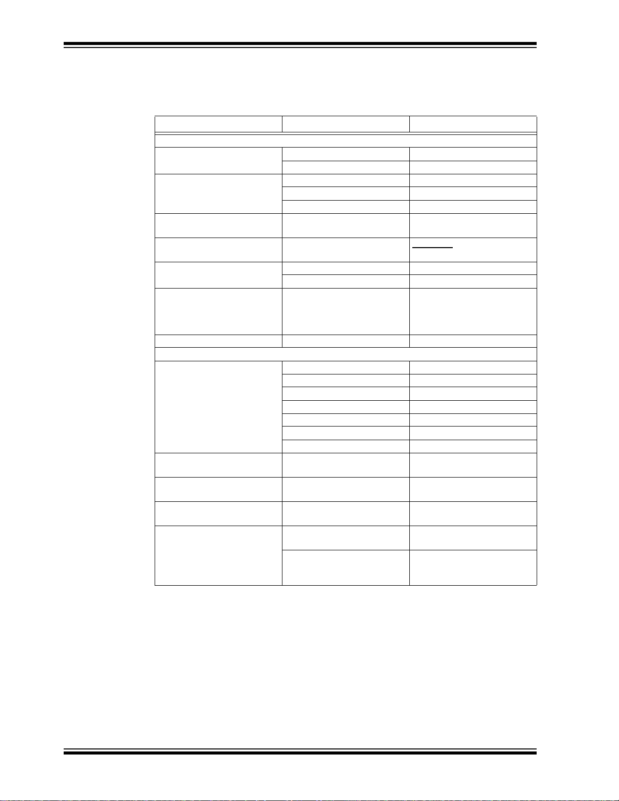
This manual uses the following documentation conventions:
DOCUMENTATION CONVENTIONS
Description Represents Examples
Arial font:
Italic characters Referenced books MPLAB® IDE User’s Guide
Emphasized text ...is the only compiler...
Initial caps A window the Output window
A dialog the Settings dialog
A menu selection select Enable Programmer
Quotes A field name in a window or
dialog
Underlined, italic text with
right angle bracket
Bold characters A dialog button Click OK
N‘Rnnnn A number in verilog format,
Text in angle brackets < > A key on the keyboard Press <Enter>, <F1>
Courier New font:
Plain Courier New Sample source code #define START
Italic Courier New A variable argument file.o, where file can be
Square brackets [ ] Optional arguments mcc18 [options] file
Curly brackets and pipe
character: { | }
Ellipses... Replaces repeated text var_name [,
A menu path File>Save
A tab Click the Power tab
where N is the total number of
digits, R is the radix and n is a
digit.
Filenames autoexec.bat
File paths c:\mcc18\h
Keywords _asm, _endasm, static
Command-line options -Opa+, -Opa-
Bit values 0, 1
Constants 0xFF, ‘A’
Choice of mutually exclusive
arguments; an OR selection
Represents code supplied by
user
“Save project before build”
4‘b0010, 2‘hF1
any valid filename
[options]
errorlevel {0|1}
var_name...]
void main (void)
{ ...
}
DS51801A-page 2 © 2009 Microchip Technology Inc.
Page 7

RECOMMENDED READING
This user's guide describes how to use MCP6V01 Input Offset Demo Board. Other
useful documents are listed below. The following Microchip documents are available
and recommended as supplemental reference resources.
MCP6V01/2/3 Data Sheet, “300 µA, Auto-Zeroed Op Amps”, DS22058
Gives detailed information on one op amp family that is used on the MCP6V01 Input
Offset Demo Board.
MCP6021/1R/2/3/4 Data Sheet, “Rail-to-Rail Input/Output, 10 MHz Op Amps”,
DS21685
Gives detailed information on another op amp family that is used on the MCP6V01
Input Offset Demo Board.
AN1177 Application Note, “Op Amp Precision Design: DC Errors”, DS01177
Discusses how to achieve high DC accuracy in op amp circuits. Also discusses the
relationship between an op amp’s input offset voltage (V
Open-Loop Gain and V
THE MICROCHIP WEB SITE
Microchip provides online support via our web site at www.microchip.com. This web
site is used as a means to make files and information easily available to customers.
Accessible by using your favorite Internet browser , the web site contains the following
information:
• Product Support – Data sheets and errata, application notes and sample
programs, design resources, user’s guides and hardware support documents,
latest software releases and archived software
• General Technical Support – Frequently Asked Questions (FAQs), technical
support requests, online discussion groups, Microchip consultant program
member listing
• Business of Microchip – Product selector and ordering guides, latest Microchip
press releases, listing of seminars and events, listings of Microchip sales offices,
distributors and factory representatives
Drift over Temperature.
OS
), CMRR, PSRR,
OS
Preface
CUSTOMER SUPPORT
Users of Microchip products can receive assistance through several channels:
• Distributor or Representative
• Local Sales Office
• Field Application Engineer (FAE)
• Technical Support
• Development Systems Information Line
Customers should contact their distributor, representative or field application engineer
for support. Local sales offices are also available to help customers. A listing of sales
offices and locations is included in the back of this document.
Technical support is available through the web site at: http://support.microchip.com
© 2009 Microchip Technology Inc. DS51801A-page 3
Page 8

MCP6V01 Input Offset Demo Board User’s Guide
DOCUMENT REVISION HISTORY
Revision A (March 2009)
• Initial Release of this Document.
DS51801A-page 4 © 2009 Microchip Technology Inc.
Page 9

Chapter 1. Product Overview
1.1 INTRODUCTION
The MCP6V01 Input Offset Demo Board is described by the following:
• Assembly # : 102-00227-R3
• Order # : MCP6V01DM-VOS
• Name: MCP6V01 Input Offset Demo Board
Items discussed in this chapter include:
• Kit Contents
• Intended Use
• Description
1.2 KIT CONTENTS
This MCP6V01 Input Offset Demo Board Kit includes:
• Assembled Printed Circuit Board (PCB)
• Important Information “Read First”
• Analog and Interface Products Demonstration Boards CD-ROM (DS21912)
Includes:
- MCP6V01 Input Offset Demo Board User’s Guide, (DS51801)
MCP6V01 INPUT OFFSET
DEMO BOARD USER’S GUIDE
FIGURE 1-1: MCP6V01 Input Offset Demo Board Contents.
© 2009 Microchip Technology Inc. DS51801A-page 5
Page 10

MCP6V01 Input Offset Demo Board User’s Guide
Outputs
GND
V
CM
V
DD
GND
V
M
VDD/2
Inputs
DUT
Diff. Amp.
VDD/2
Reference
V
CM
Reference
(buffered)
(buffered)
High Gain
Feedback
Network
V
REF
.
V
CM
1.3 INTENDED USE
The MCP6V01 Input Offset Demo Board is intended to provide a simple means to
measure the MCP6V01/2/3 op amp’s input offse t voltage ( V
conditions. This V
sheet plus changes due to power supply voltage (PSRR), common mode voltage
(CMRR), output voltage (A
1.4 DESCRIPTION
Figure 1-2 sho ws th e blo ck dia gr a m fo r the MCP6 V0 1 In pu t Offset Demo Boar d.
includes the specified input offset voltage va lue found in the dat a
OS
) and temperature (ΔVOS/ΔTA).
OL
) under a variety of bias
OS
FIGURE 1-2: Block Diagram.
This circuit does the following:
• Supports Microchip’s auto-zeroed, single op amps:
-SOIC-8 package
- Used as both Device Under Test (DUT) and in a difference amplifier
• Test points for connecting lab equipment
• Single supply configuration
• The bias inputs V
•The V
/2 Reference uses a resistor ladder to divide VDD in half, then buffers that
DD
, VCM and GND set the conditions for the DUT
DD
voltage with an op amp in unity gain
•The V
Reference:
CM
- Has a resistor divider at the input that sets V
CM=VDD
/2 when that input is left
open
- When V
effect on V
-VCM is buffered
is driven by an external voltage source, the resistor divider has n o
CM
CM
• The High Gain Feedback Network and DUT together:
- Have a noise gain of G
≈ 10.0 kV/V
N
- Have a common mode gain of 1 V/V
- Produce an output voltage of G
NVOS+VCM
DS51801A-page 6 © 2009 Microchip Technology Inc.
Page 11

Product Overview
• The Difference Amplifier (Diff. Amp.):
- Rejects the DUT’s common mode output (V
- Provides additional gain (G
≈ 10.0 V/V) to the term GNVOS at the DUT’s
DA
output
- Shifts the output so it is centered on the reference V
- Produce an output voltage of G
DAGNVOS+VDD
The inputs:
• Allow the DUT to be biased at most valid bias points
• Allow V
to set by the circuit at VDD/2, or set by the user
CM
The outputs:
• Make it easy to measure the important bias voltages V
• Make it easy to measure VM–VDD/2 = GDAGNV
CM
)
/2
OS
REF=VDD
/2 and V
DD
/2
CM
© 2009 Microchip Technology Inc. DS51801A-page 7
Page 12

MCP6V01 Input Offset Demo Board User’s Guide
NOTES:
DS51801A-page 8 © 2009 Microchip Technology Inc.
Page 13

Chapter 2. Installation and Operation
Power Supply
Power Supply
VCM – GND
VDD – GND
Voltmeter
VDD/2 – GND
Voltmeter
VM –VDD/2
Voltmeter
VCM – GND
Voltmeter
VO1–GND
2.1 INTRODUCTION
This chapter shows how to set up the MCP6V01 Input Offset Demo Board. Items
discussed in this chapter include:
• Required Tools
• Connecting the Lab Equipment
• Operating Conditions
• Calculating the DUT’s Input Offset Voltage (V
• Converting Input Offset Voltage to Other Parameters
• Reducing the Measurement Noise
2.2 REQUIRED TOOLS
• Lab Power Supplies:
- Two outputs
- 0V to 5.5V minimum range
- Adjustable
• One Voltmeter:
- 1 mV resolution
- -6V to +6V minimum range
- Differential measurement (e.g., hand held meter)
MCP6V01 INPUT OFFSET
DEMO BOARD USER’S GUIDE
)
OS
2.3 CONNECTING THE LAB EQUIPMENT
Lab equipment is connected to this board as shown in F igure 2-1. The (surface mount)
test points allow lab equipment to be connected to these boards. The power supplies
are connected at the right. The voltmeter is connected at the four different points
shown.
FIGURE 2-1: Board Connections for the MCP6V01 Input Offset Demo Board.
© 2009 Microchip Technology Inc. DS51801A-page 9
Page 14

MCP6V01 Input Offset Demo Board User’s Guide
V
OST
VMVDD2⁄–()1GDAG
N
()⁄()⋅=
Where:
1/(G
DAGN
) ≈ 10.0 µV/V
2.4 OPERATING CONDITIONS
This board works most effectively at room temperature (near +25°C). Measurements
at other temperatures should be done in an oven where the air velocity is minimal.
The power supply (V
The common mode voltage (V
operation of this demo board.
2.5 CALCULATING THE DUT’S INPUT OFFSET VOLTAGE
) should be between 1.8V and 5.5V.
DD
) needs to be between 0.3V and VDD– 0.3V for proper
CM
The DUT’s total input offset voltage (V
) can be calculated from a measurement as
OST
shown in Equation 2-1.
EQUATION 2-1:
2.6 CONVERTING INPUT OFFSET VOLTAGE TO OTHER PARAMETERS
2.6.1 Theory
Changing the bias voltages changes the input offset voltage. Microchip’s application
note AN1 177 discusses in detail how these changes in V
found in our data sheets. The following list summarizes the p arameters that contribute
to V
OST
:
• Specified Input Offset Voltage:
-V
= Input offset at the specified bias point
OS
• DC Common Mode Rejection Ratio:
- CMRR = ΔV
CM
/ΔV
OS
• DC Power Supply Rejection Ratio:
- PSRR = (ΔV
– ΔVSS)/ΔV
DD
OS
• DC Open-Loop Gain:
-A
OL
= ΔV
OUT
/ΔV
OS
• Input Offset Drift over Temperature:
- ΔV
OS
/ΔT
A
are related to specifications
OS
DS51801A-page 10 © 2009 Microchip Technology Inc.
Note: The data sheet Input Of fset Voltage (VOS) specification applies to one bias
point and temperature only. The total input offset voltage (V
V
and other changes in input offset as bias voltages and temperature
OS
) includes
OST
change.
Page 15
Installation and Operation
Given:
Then:
V
OST
=0.5µV, VCM=0V
V
OST
=1.0µV, VCM=5V
ΔV
OST
=0.5µV
ΔV
CM
=5.0V
CMRR = 5.0V / 0.5 µV
=10V/µV
= 140 dB
Example 2-1 gives an example of how V
voltage (V
CM
).
changes with the common mode input
OST
EXAMPLE 2-1: COMMON MODE CHANGE EXAMPLE
2.6.2 Application
When the common mode voltage (VCM) is changed on this demo board, the output
voltage (V
to independently change V
Open-Loop Gain (A
Note: V
) is forced to change by the same amount. There is no means provided
OUT
) effect from the CMRR effect using this board.
OL
cannot be changed independently of VCM, so AOL and CMRR cannot
OUT
CM
and V
. Thus, it is not possible to separate the
OUT
be distinguished using this circuit.
Since A
attribute most of the change to CMRR and ignore A
is usually much better than CMRR for the MCP6V0X op amps, we can
OL
in most cases. Table 2-1 shows
OL
one possible measurement matrix that will allow the user to estimate key parameters
for the DUT.
TABLE 2-1: MEASUREMENT MATRIX
Operating Inputs
(Note 1)
V
T
A
(°C)
DD
(V)
+25 5.5 OFF V
1.8 VDD/3 V
-40 5.5 VDD/3 V
+85 VDD/3 V
+125 VDD/3 V
V
CM
(V)
/3 V
V
DD
0.5 V
5.0 V
0.3 V
1.5 V
Symbol Comments
M1
M2
M3
M4
M5
M6
M7
M8
M9
M10
Quick Check
VOS and PSRR
CMRR and A
VOS and PSRR
CMRR and A
VOS at temperature and ΔVOS/ΔT
Note 1: VSS=GND=0V. VCM= OFF means that the its power supply is off (VCM=VDD/2).
V
≈ VCM.
OUT
Measurement
OL
OL
A
Based on these measurements, we can make the following estimates, where the
V
values are calculated from the measured VMk values (see Equation 2-1):
OST_k
© 2009 Microchip Technology Inc. DS51801A-page 11
Page 16

MCP6V01 Input Offset Demo Board User’s Guide
TABLE 2-2: ESTIMATES
Operating Inputs Estimate
V
DD
(V)
1.8 and 5.5 -40 to +125 1/AOL= 0, by assumption µV/V
5.5 -40 V
1.8 +25 VOS=V
Note 1: V
OST_k
Obviously, other values of T
T
A
(°C)
+25 1/PSRR = (V
+25 V
+85 VOS=V
+125 VOS=V
-40 to +125 ΔV
+25 1/CMRR = {(V
is calculated from VMk using Equation 2-1.
, VDD, … can be used instead, with the proper adjustment s
A
/ΔTA=(V
OS
1/CMRR = (V
to these equations.
2.7 REDUCING THE MEASUREMENT NOISE
The noise seen in the measurements is a result of the design choices made for the
MCP6V01 Input Offset Demo Board. The component s R12 and C5 set a lowpass po le
at 0.16 Hz, which gives reasonable noise performance (±0.2 µV
of the DUT) and settling time (1 to 2 seconds).
To achieve lower noise in your results, average many measurements together. For
instance, measuring the output (V
samples) should produce an estimate with noise √16 = 4 times lower (i.e., ±0.05 µV
There is a practical limit on increasing the sample rate; the noise does not improve
significantly after a certain point. The analog lowpass pole at 0.16 Hz causes closely
spaced samples to be correlated. To avoid the overhead caused by sampling too fast,
keep the sampling period near or above the pole’s time constant (1.0s); this gives a
minimum sample rate of 1 sample per second.
M–VDD
Equations (Note 1) Units
)/(3.7V) µV/V
) / (165°C) µV/°C
)/(4.5V) µV/V
)/(1.2V) µV/V
referred to the input
PK
OS
OS
OST_2–VOST_5
=V
OST_8
=V
OST_2
OST_9
OST_10
OST_10–VOST_8
OST_4–VOST_3
OST_5
OST_7–VOST_6
/2) once a second for 16 seconds (16
µV
µV
µV
µV
µV
PK
).
Note: Sampling much faster than 1 SPS will not improve the averaged noise of
this board’s output significantly.
DS51801A-page 12 © 2009 Microchip Technology Inc.
Page 17

Chapter 3. Possible Modifications
Label
DUT’s Pin 1
Reference Designator
3.1 INTRODUCTION
This chapter shows simple modifications to the MCP6V01 Input Offset Demo Board:
• Changing the DUT
• Connecting a Chip Select Pin to Ground
3.2 CHANGING THE DUT
Change the DUT (see Figure 3-1) to the MCP6V06 Op Amp as follows:
1. Remove U1 from the PCB, using a de-soldering tool.
2. Solder a MCP6V06 op amp in its place. Use a MCP6V06 in a SOIC-8 package.
Pin 1 is next to the U1 reference designator on the PCB (not next to the DUT
label)
MCP6V01 INPUT OFFSET
DEMO BOARD USER’S GUIDE
FIGURE 3-1: Location and Orientation of DUT.
© 2009 Microchip Technology Inc. Draft DS51801A-page 13
Page 18
MCP6V01 Input Offset Demo Board User’s Guide
DUT’s Pin 8 Ground Via
3.3 CONNECTING A CHIP SELECT PIN TO GROUND
The DUT can be changed to the MCP6V03 or MCP6V08 op amps with chip select. If
desired, their Chip Select pin (pin 8) can be forced to ground. This is done as follows
(see Figure 3-2):
1. Solder one end of a wire to the DUT’s pin 8. Pin 8 is next to the U1 reference
designator on the PCB (not next to the DUT label)
2. Solder the other end of the wire the closest ground via on the PCB. The striped
green arrow to the right in the figure shows the location. The solid green curve
represents the wire.
FIGURE 3-2: Location and Orientation of DUT.
DS51801A-page 14 Draft © 2009 Microchip Technology Inc.
Page 19

Appendix A. Schematics and Layouts
A.1 INTRODUCTION
This appendix contains the schematics and layouts for the MCP6V01 Input Offset
Demo Board.
The Gerber files for this board are available on the Microchip website
(www.microchip.com) and are contained in the “00227R3_Gerbers.zip” zip file .
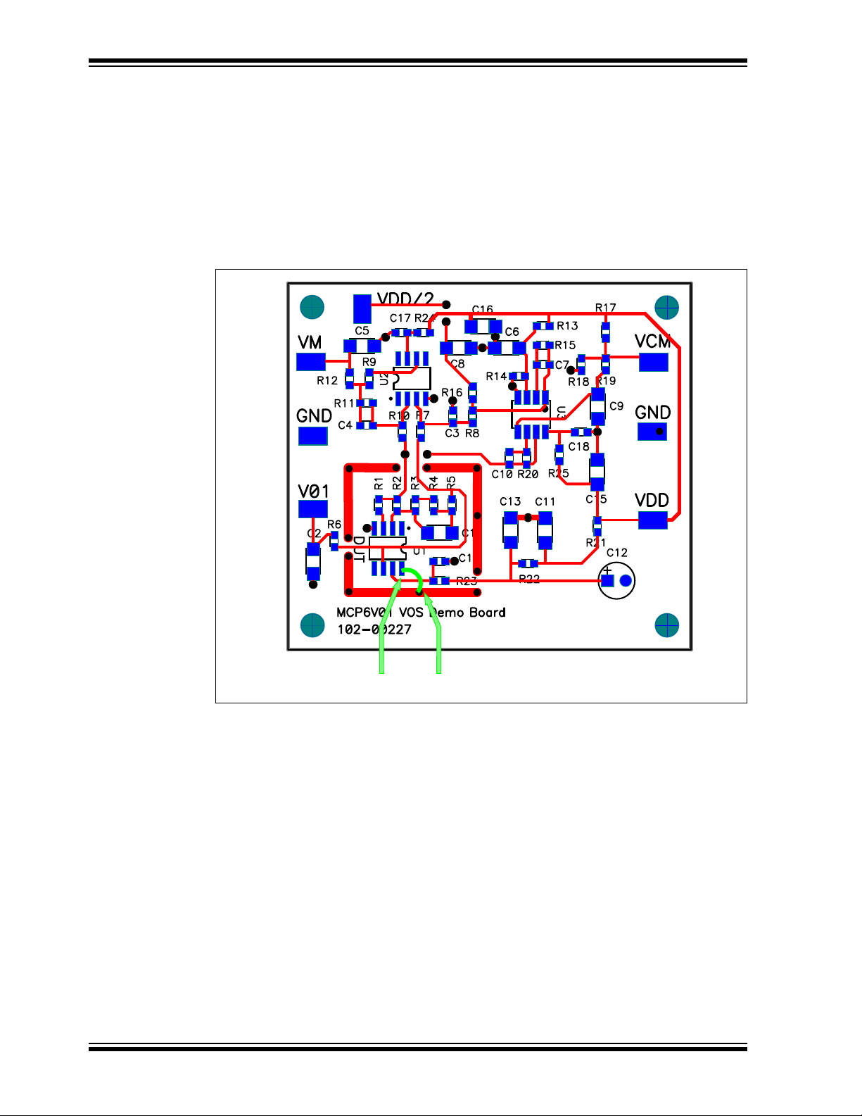
A.2 SCHEMATIC
See below the circuit diagram. On the left is the DUT (U1), which produces the common
mode voltage plus the DUT’s input offset (V
difference amplifier that amplifies and level shifts the DUT’s output minus the
mid-supply reference voltage. On the top ri ght is the mid-supply reference (V
buffer. On the middle right is the common mode voltage reference (VCM) with buffer.
On the bottom are the supply bypass capacitors and filter resistors.
MCP6V01 INPUT OFFSET
DEMO BOARD USER’S GUIDE
) times a gain. In the middle is the
OS
/2) and
DD
© 2009 Microchip Technology Inc. DS51801A-page 15
Page 20

MCP6V01 Input Offset Demo Board User’s Guide
M
A.2 BOARD SCHEMATIC (Continued)
DS51801A-page 16 © 2009 Microchip Technology Inc.
Page 21

Schematics and Layouts
A.3 COMBINATION OF THE TOP SILK SCREEN AND TOP METAL LAYERS
A.4 TOP SILK SCREEN
© 2009 Microchip Technology Inc. DS51801A-page 17
Page 22
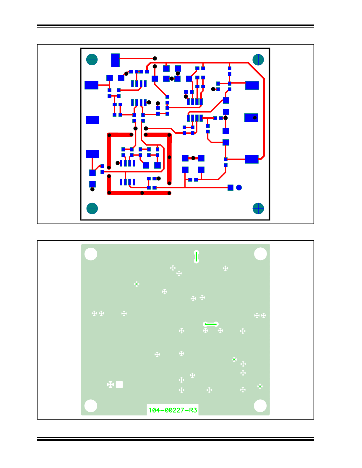
MCP6V01 Input Offset Demo Board User’s Guide
A.5 TOP METAL LAYER
A.6 BOTTOM METAL LAYER
DS51801A-page 18 © 2009 Microchip Technology Inc.
Page 23

MCP6V01 INPUT OFFSET
DEMO BOARD USER’S GUIDE
Appendix B. Bill Of Materials (BOM)
B.1 MCP6V01 INPUT OFFSET DEMO BOARD BOM
The BOM in Table B-1 corresponds to Figure 2-1; it shows all of the components
assembled on the PCB. Table B-2 shows additional parts that come in the ESD
protection bag that the user, if needed, installs.
TABLE B-1: BILL OF MATERIALS FOR ASSEMBLED PCB
Qty Reference Description Manufacturer Part Number
7 C3, C4, C7, C10,
C14, C17, C18
5 C1, C2, C8, C13, C16 1.0 µF, 1206 SMD, X7R, 16V, 10% ECJ-3YB1C105K
5 C5, C6, C9, C11, C15 10 µF, 1206 SMD, X7R, 16V, 10% ECJ-3YX1C106K
1 C12 100 µF, Radial, Electrolytic, 10 V, 20% EEU-FC1A101S
1 PCB 2 layer PCB (2.20 in × 2.00 in) n/a n/a
2 R7, R10 33.2 kΩ, 0603 SMD, 0.1%, 25 ppm/°C,
2 R8, R11 332 kΩ, 0603 SMD, 0.1%, 25 ppm/°C,
3 R23, R24, R25 10.0Ω, 0603 SMD, 1%, 1/10W Panasonic-ECG ERJ-3EKF10R0V
2 R1, R2 20.0Ω, 0603 SMD, 1%, 1/10W ERJ-3EKF20R0V
2 R21, R22 49.9Ω, 0603 SMD, 1%, 1/10W ERJ-3EKF49R9V
1R4 1.00kΩ, 0603 SMD, 1%, 1/10W ERJ-3EKF1001V
2 R5, R9 3.01 kΩ, 0603 SMD, 1%, 1/10W ERJ-3EKF3011V
1 R19 10.0 kΩ, 0603 SMD, 1%, 1/10W ERJ-3EKF1002V
5 R6, R12, R15, R16,
R20
2 R17, R18 182 kΩ, 0603 SMD, 1%, 1/10W ERJ-3EKF1823V
1 R3 196 kΩ, 0603 SMD, 1%, 1/10W ERJ-3EKF1963V
2 R13, R14 200 kΩ, 0603 SMD, 1%, 1/10W ERJ-3EKF2003V
2 U1, U2 MCP6V01, SOIC-8, Single Op Amp Microchip
1 U3 MCP6002, SOIC-8, Dual Op Amp MCP6002-E/SN
7 TP1 – TP7 SMD, Test Point Keystone
Note 1: The components listed in this Bill of Materials are representative of the PCB assembly. The released BOM
used in manufacturing uses all RoHS-compliant components.
100 nF, 060 3 SMD, X7R, 16V, 10% Panasonic
Susumu Co. Ltd. RG1608P-3322-B-T5
1/10W
1/10W
100 kΩ, 0603 SMD, 1%, 1/10W ERJ-3EKF1003V
Technology Inc.
Electronics
®
-ECG ECJ-1VB1C104K
RG1608P-3323-B-T5
MCP6V01-E/SN
®
5016
TABLE B-2: BILL OF MATERIALS FOR LOOSE PARTS IN BAG
Qty. Reference Designator Description Manufacturer Part Number
4 (for PCB mounting) Stand-off, Hex, 0.500", 4 × 40 Thread,
Nylon, 0.285" max. O.D.
4 (for PCB mounting) Machine Screw, Phillips, 4 × 40 Thread,
1/4" long, Nylon
© 2009 Microchip Technology Inc. DS51801A-page 19
Keystone
Electronics
Building
Fasteners
1902C
NY PMS 440 0025 PH
Page 24

WORLDWIDE SALES AND SERVICE
AMERICAS
Corporate Office
2355 West Chandler Blvd.
Chandler, AZ 85224-6199
Tel: 480-792-7200
Fax: 480-792-7277
Technical Support:
http://support.microchip.com
Web Address:
www.microchip.com
Atlanta
Duluth, GA
Tel: 678-957-9614
Fax: 678-957-1455
Boston
Westborough, MA
Tel: 774-760-0087
Fax: 774-760-0088
Chicago
Itasca, IL
Tel: 630-285-0071
Fax: 630-285-0075
Cleveland
Independence, OH
Tel: 216-447-0464
Fax: 216-447-0643
Dallas
Addison, TX
Tel: 972-818-7423
Fax: 972-818-2924
Detroit
Farmington Hills, MI
Tel: 248-538-2250
Fax: 248-538-2260
Kokomo
Kokomo, IN
Tel: 765-864-8360
Fax: 765-864-8387
Los Angeles
Mission Viejo, CA
Tel: 949-462-9523
Fax: 949-462-9608
Santa Clara
Santa Clara, CA
Tel: 408-961-6444
Fax: 408-961-6445
Toronto
Mississauga, Ontario,
Canada
Tel: 905-673-0699
Fax: 905-673-6509
ASIA/PACIFIC
Asia Pacific Office
Suites 3707-14, 37th Floor
Tower 6, The Gateway
Harbour City, Kowloon
Hong Kong
Tel: 852-2401-1200
Fax: 852-2401-3431
Australia - Sydney
Tel: 61-2-9868-6733
Fax: 61-2-9868-6755
China - Beijing
Tel: 86-10-8528-2100
Fax: 86-10-8528-2104
China - Chengdu
Tel: 86-28-8665-5511
Fax: 86-28-8665-7889
China - Hong Kong SAR
Tel: 852-2401-1200
Fax: 852-2401-3431
China - Nanjing
Tel: 86-25-8473-2460
Fax: 86-25-8473-2470
China - Qingdao
Tel: 86-532-8502-7355
Fax: 86-532-8502-7205
China - Shanghai
Tel: 86-21-5407-5533
Fax: 86-21-5407-5066
China - Shenyang
Tel: 86-24-2334-2829
Fax: 86-24-2334-2393
China - Shenzhen
Tel: 86-755-8203-2660
Fax: 86-755-8203-1760
China - Wuhan
Tel: 86-27-5980-5300
Fax: 86-27-5980-5118
China - Xiamen
Tel: 86-592-2388138
Fax: 86-592-2388130
China - Xian
Tel: 86-29-8833-7252
Fax: 86-29-8833-7256
China - Zhuhai
Tel: 86-756-3210040
Fax: 86-756-3210049
ASIA/PACIFIC
India - Bangalore
Tel: 91-80-3090-4444
Fax: 91-80-3090-4080
India - New Delhi
Tel: 91-11-4160-8631
Fax: 91-11-4160-8632
India - Pune
Tel: 91-20-2566-1512
Fax: 91-20-2566-1513
Japan - Yokohama
Tel: 81-45-471- 6166
Fax: 81-45-471-6122
Korea - Daegu
Tel: 82-53-744-4301
Fax: 82-53-744-4302
Korea - Seoul
Tel: 82-2-554-7200
Fax: 82-2-558-5932 or
82-2-558-5934
Malaysia - Kuala Lumpur
Tel: 60-3-6201-9857
Fax: 60-3-6201-9859
Malaysia - Penang
Tel: 60-4-227-8870
Fax: 60-4-227-4068
Philippines - Manila
Tel: 63-2-634-9065
Fax: 63-2-634-9069
Singapore
Tel: 65-6334-8870
Fax: 65-6334-8850
Taiwan - Hsin Chu
Tel: 886-3-6578-300
Fax: 886-3-6578-370
Taiwan - Kaohsiung
Tel: 886-7-536-4818
Fax: 886-7-536-4803
Taiwan - Taipei
Tel: 886-2-2500-6610
Fax: 886-2-2508-0102
Thailand - Bangkok
Tel: 66-2-694-1351
Fax: 66-2-694-1350
EUROPE
Austria - Wels
Tel: 43-7242-2244-39
Fax: 43-7242-2244-393
Denmark - Copenhagen
Tel: 45-4450-2828
Fax: 45-4485-2829
France - Paris
Tel: 33-1-69-53-63-20
Fax: 33-1-69-30-90-79
Germany - Munich
Tel: 49-89-627-144-0
Fax: 49-89-627-144-44
Italy - Milan
Tel: 39-0331-742611
Fax: 39-0331-466781
Netherlands - Drunen
Tel: 31-416-690399
Fax: 31-416-690340
Spain - Madrid
Tel: 34-91-708-08-90
Fax: 34-91-708-08-91
UK - Wokingham
Tel: 44-118-921-5869
Fax: 44-118-921-5820
03/26/09
DS51801A-page 20 © 2009 Microchip Technology Inc.
 Loading...