

Page 1
MCP661
Line Driver
Demo Board
User’s Guide
© 2009 Microchip Technology Inc. DS51868A
Page 2
Note the following details of the code protection feature on Microchip devices:
• Microchip products meet the specification contained in their particular Microchip Data Sheet.
• Microchip believes that its family of products is one of the most secure families of its kind on the market today, when used in the
intended manner and under normal conditions.
• There are dishonest and possibly illegal methods used to breach the code protection feature. All of these methods, to our
knowledge, require using the Microchip products in a manner outside the operating specifications contained in Microchip’s Data
Sheets. Most likely, the person doing so is engaged in theft of intellectual property.
• Microchip is willing to work with the customer who is concerned about the integrity of their code.
• Neither Microchip nor any other semiconductor manufacturer can guarantee the security of their code. Code protection does not
mean that we are guaranteeing the product as “unbreakable.”
Code protection is constantly evolving. We at Microchip are committed to continuously improving the code protection features of our
products. Attempts to break Microchip’s code protection feature may be a violation of the Digital Millennium Copyright Act. If such acts
allow unauthorized access to your software or other copyrighted work, you may have a right to sue for relief under that Act.
Information contained in this publication regarding device
applications and the like is provided only for your convenience
and may be superseded by updates. It is your responsibility to
ensure that your application meets with your specifications.
MICROCHIP MAKES NO REPRESENTATIONS OR
WARRANTIES OF ANY KIND WHETHER EXPRESS OR
IMPLIED, WRITTEN OR ORAL, STATUTORY OR
OTHERWISE, RELATED TO THE INFORMATION,
INCLUDING BUT NOT LIMITED TO ITS CONDITION,
QUALITY, PERFORMANCE, MERCHANTABILITY OR
FITNESS FOR PURPOSE. Microchip disclaims all liability
arising from this information and its use. Use of Microchip
devices in life support and/or safety applications is entirely at
the buyer’s risk, and the buyer agrees to defend, indemnify and
hold harmless Microchip from any and all damages, claims,
suits, or expenses resulting from such use. No licenses are
conveyed, implicitly or otherwise, under any Microchip
intellectual property rights.
Trademarks
The Microchip name and logo, the Microchip logo, dsPIC,
K
EELOQ, KEELOQ logo, MPLAB, PIC, PICmicro, PICSTART,
rfPIC and UNI/O are registered trademarks of Microchip
Technology Incorporated in the U.S.A. and other countries.
FilterLab, Hampshire, HI-TECH C, Linear Active Thermistor,
MXDEV, MXLAB, SEEVAL and The Embedded Control
Solutions Company are registered trademarks of Microchip
Technology Incorporated in the U.S.A.
Analog-for-the-Digital Age, Application Maestro, CodeGuard,
dsPICDEM, dsPICDEM.net, dsPICworks, dsSPEAK, ECAN,
ECONOMONITOR, FanSense, HI-TIDE, In-Circuit Serial
Programming, ICSP, ICEPIC, Mindi, MiWi, MPASM, MPLAB
Certified logo, MPLIB, MPLINK, mTouch, Omniscient Code
Generation, PICC, PICC-18, PICkit, PICDEM, PICDEM.net,
PICtail, PIC
32
logo, REAL ICE, rfLAB, Select Mode, Total
Endurance, TSHARC, WiperLock and ZENA are trademarks
of Microchip T echnology Incorporated in the U.S.A. and other
countries.
SQTP is a service mark of Microchip Technology Incorporated
in the U.S.A.
All other trademarks mentioned herein are property of their
respective companies.
© 2009, Microchip Technology Incorporated, Printed in the
U.S.A., All Rights Reserved.
Printed on recycled paper.
Microchip received ISO/TS-16949:2002 certification for its worldwide
headquarters, design and wafer fabrication facilities in Chandler and
T empe, Arizona; Gresham, Oregon and design centers in California
and India. The Company’s quality system processes and procedures
are for its PIC
devices, Serial EEPROMs, microperipherals, nonvolatile memo ry and
analog products. In addition, Microchip’s quality system for the desig n
and manufacture of development systems is ISO 9001:2000 certified.
®
MCUs and dsPIC® DSCs, KEELOQ
®
code hopping
DS51868A-page 2 © 2009 Microchip Technology Inc.
Page 3

MCP661 LINE DRIVER DEMO
BOARD USER ’S GUIDE
Table of Contents
Preface ...........................................................................................................................1
Introduction............................................................................................................1
Document Layout..................................................................................................1
Conventions Used in this Guide............................................................................2
Recommended Reading........................................................................................3
The Microchip Web Site........................................................................................ 3
Customer Support.................................................................................................3
Document Revision History...................................................................................3
Chapter 1. Product Overview
1.1 Introduction .....................................................................................................5
1.2 Kit Contents ....................................................................................................5
1.3 Intended Use ..................................................................................................6
1.4 Description .....................................................................................................6
Chapter 2. Installation and Operation
2.1 Introduction .....................................................................................................9
2.2 Required Tools ............................................................................................... 9
2.3 Configuring the Lab Equipment and PCB ....................................................10
Appendix A. Schematics and Layouts
A.1 Introduction ..................................................................................................11
A.2 Board – Schematic .......................................................................................12
A.3 Board – Top Silk Screen, Top Solder Mask and Top Metal ....................13
A.4 Board – Top Silk Screen and Top Solder Mask ...........................................13
A.5 Board – Bottom Metal Layer (Top View) ......................................................14
A.6 Board – Bottom Metal Layer (Bottom View) .................................................14
Appendix B. Bill Of Materials (BOM)
B.1 MCP661 Line Driver Demo Board BOM ...................................................... 15
Worldwide Sales and Service ....................................................................................16
© 2009 Microchip Technology Inc. DS51868A-page 3
Page 4

MCP661 Line Driver Demo Board User’s Guide
NOTES:
DS51868A-page 4 © 2009 Microchip Technology Inc.
Page 5
MCP661 LINE DRIVER DEMO
BOARD USER ’S GUIDE
Preface
NOTICE TO CUSTOMERS
All documentation becomes dated, and this manual is no exception. Microchip tools and
documentation are constantly evolving to meet customer needs, so some actual dialogs
and/or tool descriptions may differ from those in this document. Please refer to our web site
(www.microchip.com) to obtain the latest documentation available.
Documents are identified with a “DS” number. This number is located on the bottom of each
page, in front of the page number. The numbering convention for the DS number is
“DSXXXXXA”, where “XXXXX” is the document number and “A” is the revision level of the
document.
For the most up-to-date information on development tools, see the MPLAB
Select the Help menu, and then Topics to open a list of available on-line help files.
®
IDE on-line help.
INTRODUCTION
This chapter contains general information that will be useful to know before using the
MCP661 Line Driver Demo Board. Items discussed in this chapter include:
• Document Layout
• Conventions Used in this Guide
• Recommended Reading
• The Microchip Web Site
• Customer Support
• Document Revision History
DOCUMENT LAYOUT
This document describes how to use the MCP661 Lin e Driver Dem o Boar d. The
manual layout is as follows:
• Chapter 1. “Product Overview” - Important information about the MCP661 Line
Driver Demo Board.
• Chapter 2. “Installation and Operation” – Covers the initial set-up of the
MCP661 Line Driver Demo Board. It lists the required tools, shows how to set up
the board and how to connect lab equipmen t. It then demonstrates ho w to use this
board.
• Appendix A. “Schematics and Layouts” – Shows the schematic and board
layouts for the MCP661 Line Driver Demo Board.
• Appendix B. “Bill Of Materials (BOM)” – Lists the parts used to populate the
MCP661 Line Driver Demo Board. Also lists alternate components.
© 2009 Microchip Technology Inc. DS51868A-page 5
Page 6
MCP661 Line Driver Demo Board User’s Guide
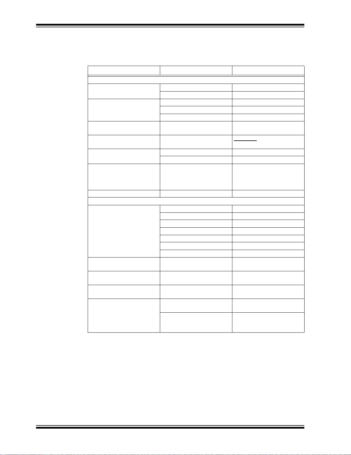
CONVENTIONS USED IN THIS GUIDE
This manual uses the following documentation conventions:
DOCUMENTATION CONVENTIONS
Description Represents Examples
Arial font:
Italic characters Referenced books MPLAB® IDE User’s Guide
Emphasized text ...is the only compiler...
Initial caps A window the Output window
A dialog the Settings dialog
A menu selection select Enable Programmer
Quotes A field name in a window or
dialog
Underlined, italic text with
right angle bracket
Bold characters A dialog button Click OK
N‘Rnnnn A number in verilog format,
Text in angle brackets < > A key on the keyboard Press <Enter>, <F1>
Courier New font:
Plain Courier New Sample source code #define START
Italic Courier New A variable argument file.o, where file can be
Square brackets [ ] Optional arguments mcc18 [options] file
Curly brackets and pipe
character: { | }
Ellipses... Replaces repeated text var_name [,
A menu path File>Save
A tab Click the Power tab
where N is the total number of
digits, R is the radix and n is a
digit.
Filenames autoexec.bat
File paths c:\mcc18\h
Keywords _asm, _endasm, static
Command-line options -Opa+, -Opa-
Bit values 0, 1
Constants 0xFF, ‘A’
Choice of mutually exclusive
arguments; an OR selection
Represents code supplied by
user
“Save project before build”
4‘b0010, 2‘hF1
any valid filename
[options]
errorlevel {0|1}
var_name...]
void main (void)
{ ...
}
DS51868A-page 6 © 2009 Microchip Technology Inc.
Page 7

RECOMMENDED READING
This user's guide describes how to use MCP661 Line Driver Demo Board. Other useful
documents are listed below. The following Microchip documents are available and
recommended as supplemental reference resources.
MCP661/2/3/5 Data Sheet, “60MHz, 6mA Op Amps”, (DS22194)
Gives detailed information on the op amp family that is used as the DUT on the
MCP661 Line Driver Demo Board.
THE MICROCHIP WEB SITE
Microchip provides online support via our web site at www.microchip.com. This web
site is used as a means to make files and information easily available to customers.
Accessible by using your favorite Internet browser , the web site contains the following
information:
• Product Support – Data sheets and errata, application notes and sample
programs, design resources, user’s guides and hardware support documents,
latest software releases and archived software
• General Technical Support – Frequently Asked Questions (FAQs), technical
support requests, online discussion groups, Microchip consultant program
member listing
• Business of Microchip – Product selector and ordering guides, latest Microchip
press releases, listing of seminars and events, listings of Microchip sales offices,
distributors and factory representatives
Preface
CUSTOMER SUPPORT
Users of Microchip products can receive assistance through several channels:
• Distributor or Representative
• Local Sales Office
• Field Application Engineer (FAE)
• Technical Support
• Development Systems Information Line
Customers should contact their distributor, representative or field application engineer
for support. Local sales offices are also available to help customers. A listing of sales
offices and locations is included in the back of this document.
Technical support is available through the web site at: http://support.microchip.com
DOCUMENT REVISION HISTORY
Revision A (November 2009)
• Initial Release of this Document.
© 2009 Microchip Technology Inc. DS51868A-page 7
Page 8

MCP661 Line Driver Demo Board User’s Guide
NOTES:
DS51868A-page 8 © 2009 Microchip Technology Inc.
Page 9

Chapter 1. Product Overview
1.1 INTRODUCTION
The MCP661 Line Driver Demo Board is described by the following:
• Assembly # : 114-00270-R1
• Order # : MCP661DM-LD
• Name: MCP661 Line Driver Demo Board
Items discussed in this chapter include:
• Kit Contents
• Intended Use
• Description
1.2 KIT CONTENTS
• Assembled printed circuit board, 102-00270
• Important Information “Read First”
MCP661 LINE DRIVER DEMO
BOARD USER ’S GUIDE
FIGURE 1-1: MCP661 Line Driver Demo Board Kit Contents.
© 2009 Microchip Technology Inc. DS51868A-page 9
Page 10

MCP661 Line Driver Demo Board User’s Guide
R
6
301Ω
R
5
301Ω
R
3
49.9Ω
R
7
49.9Ω
50Ω
TX Line
V
OUT
(50Ω Load)
V
IN
(50Ω Source)
50Ω
TX Line
U
1
MCP661
R
4
124Ω
1.3 INTENDED USE
The MCP661 Line Driver Demo Board shows the MCP661 used in a very basic
application for high speed op amps; a 50Ω line (coax) driver. It gives:
• A 30 MHz solution
• High speed PCB layout techniques
• A means to test AC response, step response and distortion
The application circuit implemented on this PCB is discussed briefly in the
MCP661/2/3/5 data sheet’s application circuit section.
1.4 DESCRIPTION
1.4.1 Simplified Circuit
Figure 1-2 shows a simplified circuit diagram of the MCP661 Line Driver Demo Board.
Details of the power supply and connectors have been left out.
FIGURE 1-2: Simplified Circuit Diagram.
The 50Ω source drives the matched 50Ω transmission line at the input; R
provides this
3
match. Thus, the input transmission line can be treated as a simple connection for
circuit analysis (ignoring the time delay).
R
provides matched input resistances for U1’s inputs. It also set a pole around
4
100 MHz, since U
U
(MCP661) is set at a gain of 2 V/V so that the overall gain is 1 V/V (R7 and the Load
1
attenuate the signal by 0.5 V/V). U
back-matched output transmission line (R
’s CCM is about 9 pF.
1
’s large output current makes it possible to drive the
1
, the 50Ω line and the 50Ω load at the far
7
end) to more than ±2V (the load at the far end sees ±1V).
U
’s output headroom limits would be VOL= -2.3V and VOH= +2.3V, leaving some
1
design room for the ±2V signal. The open-loop gain (A
) typically does not decrease
OL
significantly with a 100Ω load. The maximum power dissipated by the op amp is about
48 mW, so the temperature rise (for the MCP661 in the SOIC-8 package) is under 8°C.
The output transmision line can be treated as a simple connection for circuit analysis
(ignoring the time delay).
DS51868A-page 10 © 2009 Microchip Technology Inc.
Page 11

Product Overview
V
DDX
(+2.5V)
GND
(0V)
V
SSX
(-2.5V)
R
1
1.0Ω
R
2
1.0Ω
C
1
C
2
10 µF
10 µF
U
1
MCP661
C
3
100 nF
C
4
100 nF
1.4.2 Power Supply
Figure 1-3 shows the power supply circuitry. R1 and R2 provide high frequency isolation
of the supply lines. They also help with series resonances in the supplies. C
provide the bulk bypassing, while C
and C4 provide the local bypassing, for U1
3
(MCP661).
FIGURE 1-3: Power Supply.
and C2
1
1.4.3 Connectors and Transmission Lines
The power supplies use surface mount test points to connect to the lab supplies. The
signal input and output are connected via BNC recepticles (and coax cables) to 50Ω
lab equipment.
The PCB has two 50Ω transmission lines between the BNC recepticles and the
matching resistors (R
is a value commonly used for standard FR4 PCBs with only two layers. These lines are
as long as possible; they end at the matching resistors (to avoid pa rasitic cap acit an ce
issues).
and R7 in Figure 1-2). They are 100 mils (2.54 mm) wide, which
3
© 2009 Microchip Technology Inc. DS51868A-page 11
Page 12

MCP661 Line Driver Demo Board User’s Guide
NOTES:
DS51868A-page 12 © 2009 Microchip Technology Inc.
Page 13

Chapter 2. Installation and Operation
2.1 INTRODUCTION
This chapter shows how to set up and operate the MCP661 Line Driver Demo Board.
Items discussed in this chapter include:
• Required Tools
• Configuring the Lab Equipment and PCB
2.2 REQUIRED TOOLS
• Lab Power Supply with dual outputs (one tracks the other):
- For +2.5V, 0V and -2.5V
• Sine Wave Source (function gener ator, network analyzer, spectrum ana lyze r, etc):
- Sine wave output to 100 MHz, or so
-50Ω output impedance
- -2.5V to +2.5V minimum range
• Signal Analyzer (oscilloscope, network analyzer, spectrum analyzer, etc):
-50Ω input impedance
- At least 100 M Hz bandwidth
MCP661 LINE DRIVER DEMO
BOARD USER ’S GUIDE
© 2009 Microchip Technology Inc. DS51868A-page 13
Page 14

MCP661 Line Driver Demo Board User’s Guide
3
1 2
2.3 CONFIGURING THE LAB EQUIPMENT AND PCB
Lab equipment is connected to this board as shown in Figure 2-1. The BNC recepticles
and (surface mount) test points allow lab equipment to be connected to these boards.
FIGURE 2-1: Lab Equipment Connections.
The arrows and numbers in the drawing signify the following:
1. BNC Recepticle for V
2. BNC Recepticle for V
3. ±2.5V Power Supplies, with GND, for U1 (MCP661).
a) VDDX = +2.5V.
b) GND = 0V.
c) VSSX = -2.5V.
.
IN
OUT
.
DS51868A-page 14 © 2009 Microchip Technology Inc.
Page 15

Appendix A. Schematics and Layouts
A.1 INTRODUCTION
This appendix contains the schematic and layouts fo r the MCP661 Line Driver Demo
Board.
•Board – Schematic
•Board – Top Silk Screen, Top Solder Mask and Top Metal
•Board – Top Silk Screen and Top Solder Mask
•Board – Bottom Metal (Top View)
•Board – Bottom Metal (Bottom View)
The Gerber files for this board are available on the Microchip website
(www.microchip.com) and are contained in the zip file “00270R1_Gerbers.zip”.
MCP661 LINE DRIVER DEMO
BOARD USER ’S GUIDE
© 2009 Microchip Technology Inc. DS51868A-page 15
Page 16

MCP661 Line Driver Demo Board User’s Guide
M
A.2 BOARD – SCHEMATIC
DS51868A-page 16 © 2009 Microchip Technology Inc.
Page 17

Schematics and Layouts
A.3 BOARD – TOP SILK SCREEN, TOP SOLDER MASK AND TOP METAL
A.4 BOARD – TOP SILK SCREEN AND TOP SOLDER MASK
© 2009 Microchip Technology Inc. DS51868A-page 17
Page 18

MCP661 Line Driver Demo Board User’s Guide
A.5 BOARD – BOTTOM METAL LAYER (TOP VIEW)
A.6 BOARD – BOTTOM METAL LAYER (BOTTOM VIEW)
DS51868A-page 18 © 2009 Microchip Technology Inc.
Page 19

MCP661 LINE DRIVER DEMO
BOARD USER ’S GUIDE
Appendix B. Bill Of Materials (BOM)
B.1 MCP661 LINE DRIVER DEMO BOARD BOM
The BOM in Table B-1 shows all of the components assembled on the PCB. Table B-2
shows alternate components that can be placed on this PCB (after modification).
TABLE B-1: BILL OF MATERIALS FOR ASSEMBLED PCB
Qty.
2 C3, C4 100 nF, 0603 SMD, X7R, 16V, 10% Panaso nic
2 C1, C2 10 µF, 1206 SMD, X7R, 16V, 10% Panasonic-ECG ECJ-3YX1C106K
2 P1, P2 BNC Recepticle, 50Ω, Top Mount (
2 R3, R7 49.9Ω, 0603 SMD, 1%, 1/10W Yageo
1R4 124Ω, 0603 SMD, 1%, 1/10W Yageo RC0603FR-07124RL
2 R5, R6 301Ω, 0603 SMD, 1%, 1/10W Yageo RC0603FR-07301RL
2 R1, R2 1.0Ω, 0603 SMD, 5%, 1/10W Yageo RC0603JR-071RL
3 TP1 – TP3 SMD, Test Point Keystone Electronics
1 U1 MCP661, SOIC-8, Single Op Amp Microchip Technology Inc. MCP661-E/SN
1 PCB 2 layer PCB (2.23 in × 1.50 in) Microchip Technology Inc. 102-00270
4 (for PCB mounting) Hemispherical Bumpon Standoff,
Note 1: These are mounted on the side to reduc e strain on the cables in the lab.
Reference
Designator
0.44 in × 0.20 in
2: The components listed in this Bill of Materials are representative of the PCB assembly . The released BOM
used in manufacturing uses all RoHS-compliant components.
Description Manufacturer Part Number
®
-ECG ECJ-1VB1C104K
1
) Amphenol 031-5329-52RFX
®
3M SJ-5003 (BLACK)
RC0603FR-0749R9L
®
5016
TABLE B-2: BILL OF MATERIALS FOR ALTERNATE COMPONENTS
Qty.
0 (for PCB mounting) Stand-off, Hex, 0.500", 4 × 40 Thread, Nylon,
0 (for PCB mounting) Machine Screw, Phillips, 4 × 40 Thread,
Note 1: The components listed in this Bill of Materials are representative of the PCB assembly . The released BOM
© 2009 Microchip Technology Inc. DS51868A-page 19
Reference
Designator
0.285" max. O.D.
1/4" long, Nylon
used in manufacturing uses all RoHS-compliant components.
Description Manufacturer Part Number
Keystone
Electronics
Building
Fasteners
1902C
NY PMS 440 0025 PH
Page 20

WORLDWIDE SALES AND SERVICE
AMERICAS
Corporate Office
2355 West Chandler Blvd.
Chandler, AZ 85224-6199
Tel: 480-792-7200
Fax: 480-792-7277
Technical Support:
http://support.microchip.com
Web Address:
www.microchip.com
Atlanta
Duluth, GA
Tel: 678-957-9614
Fax: 678-957-1455
Boston
Westborough, MA
Tel: 774-760-0087
Fax: 774-760-0088
Chicago
Itasca, IL
Tel: 630-285-0071
Fax: 630-285-0075
Cleveland
Independence, OH
Tel: 216-447-0464
Fax: 216-447-0643
Dallas
Addison, TX
Tel: 972-818-7423
Fax: 972-818-2924
Detroit
Farmington Hills, MI
Tel: 248-538-2250
Fax: 248-538-2260
Kokomo
Kokomo, IN
Tel: 765-864-8360
Fax: 765-864-8387
Los Angeles
Mission Viejo, CA
Tel: 949-462-9523
Fax: 949-462-9608
Santa Clara
Santa Clara, CA
Tel: 408-961-6444
Fax: 408-961-6445
Toronto
Mississauga, Ontario,
Canada
Tel: 905-673-0699
Fax: 905-673-6509
ASIA/PACIFIC
Asia Pacific Office
Suites 3707-14, 37th Floor
Tower 6, The Gateway
Harbour City, Kowloon
Hong Kong
Tel: 852-2401-1200
Fax: 852-2401-3431
Australia - Sydney
Tel: 61-2-9868-6733
Fax: 61-2-9868-6755
China - Beijing
Tel: 86-10-8528-2100
Fax: 86-10-8528-2104
China - Chengdu
Tel: 86-28-8665-5511
Fax: 86-28-8665-7889
China - Hong Kong SAR
Tel: 852-2401-1200
Fax: 852-2401-3431
China - Nanjing
Tel: 86-25-8473-2460
Fax: 86-25-8473-2470
China - Qingdao
Tel: 86-532-8502-7355
Fax: 86-532-8502-7205
China - Shanghai
Tel: 86-21-5407-5533
Fax: 86-21-5407-5066
China - Shenyang
Tel: 86-24-2334-2829
Fax: 86-24-2334-2393
China - Shenzhen
Tel: 86-755-8203-2660
Fax: 86-755-8203-1760
China - Wuhan
Tel: 86-27-5980-5300
Fax: 86-27-5980-5118
China - Xiamen
Tel: 86-592-2388138
Fax: 86-592-2388130
China - Xian
Tel: 86-29-8833-7252
Fax: 86-29-8833-7256
China - Zhuhai
Tel: 86-756-3210040
Fax: 86-756-3210049
ASIA/PACIFIC
India - Bangalore
Tel: 91-80-3090-4444
Fax: 91-80-3090-4080
India - New Delhi
Tel: 91-11-4160-8631
Fax: 91-11-4160-8632
India - Pune
Tel: 91-20-2566-1512
Fax: 91-20-2566-1513
Japan - Yokohama
Tel: 81-45-471- 6166
Fax: 81-45-471-6122
Korea - Daegu
Tel: 82-53-744-4301
Fax: 82-53-744-4302
Korea - Seoul
Tel: 82-2-554-7200
Fax: 82-2-558-5932 or
82-2-558-5934
Malaysia - Kuala Lumpur
Tel: 60-3-6201-9857
Fax: 60-3-6201-9859
Malaysia - Penang
Tel: 60-4-227-8870
Fax: 60-4-227-4068
Philippines - Manila
Tel: 63-2-634-9065
Fax: 63-2-634-9069
Singapore
Tel: 65-6334-8870
Fax: 65-6334-8850
Taiwan - Hsin Chu
Tel: 886-3-6578-300
Fax: 886-3-6578-370
Taiwan - Kaohsiung
Tel: 886-7-536-4818
Fax: 886-7-536-4803
Taiwan - Taipei
Tel: 886-2-2500-6610
Fax: 886-2-2508-0102
Thailand - Bangkok
Tel: 66-2-694-1351
Fax: 66-2-694-1350
EUROPE
Austria - Wels
Tel: 43-7242-2244-39
Fax: 43-7242-2244-393
Denmark - Copenhagen
Tel: 45-4450-2828
Fax: 45-4485-2829
France - Paris
Tel: 33-1-69-53-63-20
Fax: 33-1-69-30-90-79
Germany - Munich
Tel: 49-89-627-144-0
Fax: 49-89-627-144-44
Italy - Milan
Tel: 39-0331-742611
Fax: 39-0331-466781
Netherlands - Drunen
Tel: 31-416-690399
Fax: 31-416-690340
Spain - Madrid
Tel: 34-91-708-08-90
Fax: 34-91-708-08-91
UK - Wokingham
Tel: 44-118-921-5869
Fax: 44-118-921-5820
03/26/09
DS51868A-page 20 © 2009 Microchip Technology Inc.
 Loading...