

Page 1

MCP651
Input Offset
Evaluation Board
User’s Guide
© 2009 Microchip Technology Inc. DS51834A
Page 2

Note the following details of the code protection feature on Microchip devices:
• Microchip products meet the specification contained in their particular Microchip Data Sheet.
• Microchip believes that its family of products is one of the most secure families of its kind on the market today, when used in the
intended manner and under normal conditions.
• There are dishonest and possibly illegal methods used to breach the code protection feature. All of these methods, to our
knowledge, require using the Microchip products in a manner outside the operating specifications contained in Microchip’s Data
Sheets. Most likely, the person doing so is engaged in theft of intellectual property.
• Microchip is willing to work with the customer who is concerned about the integrity of their code.
• Neither Microchip nor any other semiconductor manufacturer can guarantee the security of their code. Code protection does not
mean that we are guaranteeing the product as “unbreakable.”
Code protection is constantly evolving. We at Microchip are committed to continuously improving the code protection features of our
products. Attempts to break Microchip’s code protection feature may be a violation of the Digital Millennium Copyright Act. If such acts
allow unauthorized access to your software or other copyrighted work, you may have a right to sue for relief under that Act.
Information contained in this publication regarding device
applications and the like is provided only for your convenience
and may be superseded by updates. It is your responsibility to
ensure that your application meets with your specifications.
MICROCHIP MAKES NO REPRESENTATIONS OR
WARRANTIES OF ANY KIND WHETHER EXPRESS OR
IMPLIED, WRITTEN OR ORAL, STATUTORY OR
OTHERWISE, RELATED TO THE INFORMATION,
INCLUDING BUT NOT LIMITED TO ITS CONDITION,
QUALITY, PERFORMANCE, MERCHANTABILITY OR
FITNESS FOR PURPOSE. Microchip disclaims all liability
arising from this information and its use. Use of Microchip
devices in life support and/or safety applications is entirely at
the buyer’s risk, and the buyer agrees to defend, indemnify and
hold harmless Microchip from any and all damages, claims,
suits, or expenses resulting from such use. No licenses are
conveyed, implicitly or otherwise, under any Microchip
intellectual property rights.
Trademarks
The Microchip name and logo, the Microchip logo, Accuron,
dsPIC, K
EELOQ, KEELOQ logo, MPLAB, PIC, PICmicro,
PICSTART, rfPIC, SmartShunt and UNI/O are registered
trademarks of Microchip Technology Incorporated in the
U.S.A. and other countries.
FilterLab, Hampshire, Linear Active Thermistor, MXDEV,
MXLAB, SEEVAL, SmartSensor and The Embedded Control
Solutions Company are registered trademarks of Microchip
Technology Incorporated in the U.S.A.
Analog-for-the-Digital Age, Application Maestro, CodeGuard,
dsPICDEM, dsPICDEM.net, dsPICworks, dsSPEAK, ECAN,
ECONOMONITOR, FanSense, In-Circuit Serial
Programming, ICSP, ICEPIC, Mindi, MiWi, MPASM, MPLAB
Certified logo, MPLIB, MPLINK, mTouch, nanoWatt XLP,
PICkit, PICDEM, PICDEM.net, PICtail, PIC
32
logo, PowerCal,
PowerInfo, PowerMate, PowerTool, REAL ICE, rfLAB, Select
Mode, Total Endurance, TSHARC, WiperLock and ZENA are
trademarks of Microchip Technology Incorporated in the
U.S.A. and other countries.
SQTP is a service mark of Microchip Technology Incorporated
in the U.S.A.
All other trademarks mentioned herein are property of their
respective companies.
© 2009, Microchip Technology Incorporated, Printed in the
U.S.A., All Rights Reserved.
Printed on recycled paper.
Microchip received ISO/TS-16949:2002 certification for its worldwide
headquarters, design and wafer fabrication facilities in Chandler and
Tempe, Arizona; Gresham, Oregon and design centers in California
and India. The Company’s quality system processes and procedures
are for its PIC
devices, Serial EEPROMs, microperipherals, nonvolatile memory and
analog products. In addition, Microchip’s quality system for the design
and manufacture of development systems is ISO 9001:2000 certified.
®
MCUs and dsPIC® DSCs, KEELOQ
®
code hopping
DS51834A-page ii © 2009 Microchip Technology Inc.
Page 3

MCP651 INPUT OFFSET
EVALUATION BOARD
USER’S GUIDE
Table of Contents
Preface ........................................................................................................................... 1
Introduction............................................................................................................ 1
Document Layout .................................................................................................. 1
Conventions Used in this Guide ............................................................................ 2
Recommended Reading........................................................................................ 3
The Microchip Web Site ........................................................................................ 3
Customer Support ................................................................................................. 3
Document Revision History................................................................................... 4
Chapter 1. Product Overview
1.1 Introduction ..................................................................................................... 5
1.2 Kit Contents .................................................................................................... 5
1.3 Intended Use .................................................................................................. 6
1.4 Description ..................................................................................................... 6
Chapter 2. Installation and Operation
2.1 Introduction ................................................................................................... 11
2.2 Required Tools ............................................................................................. 11
2.3 Configuring the Lab Equipment and PCB .................................................... 12
2.4 Operating Conditions .................................................................................... 14
2.5 Converting to Other Parameters .................................................................. 15
2.6 Settling Time, Noise and Sampling Rate ...................................................... 17
Chapter 3. Possible Modifications
3.1 Introduction ................................................................................................... 19
3.2 Range of Parts Supported by MCP651 Input Offset Evaluation Board ........ 19
3.3 Changes to Accommodate Other DUTs ....................................................... 21
Appendix A. Schematics and Layouts
A.1 Introduction .................................................................................................. 25
A.2 Schematic and Layouts ................................................................................ 25
A.3 Board – Schematic ....................................................................................... 26
A.4 Board – Combination of the Top Silk Screen, Top Solder Mask and Top Metal
Layers ..................................................................................................... 27
A.5 Board – Top Silk Screen .............................................................................. 28
A.6 Board – Top Solder Mask and Top Metal Layer .......................................... 29
A.7 Board – Bottom Metal Layer ........................................................................ 30
© 2009 Microchip Technology Inc. DS51834A-page iii
Page 4

MCP651 Input Offset Evaluation Board User’s Guide
Appendix B. Bill Of Materials (BOM)
B.1 MCP651 Input Offset Evaluation Board BOM .............................................. 31
B.2 Adaptor Board BOM ..................................................................................... 33
Worldwide Sales and Service .....................................................................................34
DS51834A-page iv © 2009 Microchip Technology Inc.
Page 5

MCP651 INPUT OFFSET
EVALUATION BOARD
USER’S GUIDE
Preface
NOTICE TO CUSTOMERS
All documentation becomes dated, and this manual is no exception. Microchip tools and
documentation are constantly evolving to meet customer needs, so some actual dialogs
and/or tool descriptions may differ from those in this document. Please refer to our web site
(www.microchip.com) to obtain the latest documentation available.
Documents are identified with a “DS” number. This number is located on the bottom of each
page, in front of the page number. The numbering convention for the DS number is
“DSXXXXXA”, where “XXXXX” is the document number and “A” is the revision level of the
document.
For the most up-to-date information on development tools, see the MPLAB
Select the Help menu, and then Topics to open a list of available on-line help files.
®
IDE on-line help.
INTRODUCTION
This chapter contains general information that will be useful to know before using the
MCP651 Input Offset Evaluation Board. Items discussed in this chapter include:
• Document Layout
• Conventions Used in this Guide
• Recommended Reading
• The Microchip Web Site
• Customer Support
• Document Revision History
DOCUMENT LAYOUT
This document describes how to use the MCP651 Input Offset Evaluation Board. The
manual layout is as follows:
• Chapter 1. “Product Overview” - Important information about the MCP651 Input
Offset Evaluation Board.
• Chapter 2. “Installation and Operation” – Covers the initial set-up of the
MCP651 Input Offset Evaluation Board. It lists the required tools, shows how to
set up the board and how to connect lab equipment. It then demonstrates how to
use this board.
• Chapter 3. “Possible Modifications” – Shows how to modify the board for other
single Microchip op amps in SOIC-8, PDIP-8 and other packages.
• Appendix A. “Schematics and Layouts” – Shows the schematic and board
layouts for the MCP651 Input Offset Evaluation Board.
• Appendix B. “Bill Of Materials (BOM)” – Lists the parts used to populate the
MCP651 Input Offset Evaluation Board. Also lists loose parts shipped with the
board in an ESD bag, alternate components and components not populated.
© 2009 Microchip Technology Inc. DS51834A-page 1
Page 6

MCP651 Input Offset Evaluation Board User’s Guide
CONVENTIONS USED IN THIS GUIDE
This manual uses the following documentation conventions:
DOCUMENTATION CONVENTIONS
Description Represents Examples
Arial font:
Italic characters Referenced books MPLAB® IDE User’s Guide
Emphasized text ...is the only compiler...
Initial caps A window the Output window
A dialog the Settings dialog
A menu selection select Enable Programmer
Quotes A field name in a window or
dialog
Underlined, italic text with
right angle bracket
Bold characters A dialog button Click OK
N‘Rnnnn A number in verilog format,
Text in angle brackets < > A key on the keyboard Press <Enter>, <F1>
Courier New font:
Plain Courier New Sample source code #define START
Italic Courier New A variable argument file.o, where file can be
Square brackets [ ] Optional arguments mcc18 [options] file
Curly brackets and pipe
character: { | }
Ellipses... Replaces repeated text var_name [,
A menu path File>Save
A tab Click the Power tab
where N is the total number of
digits, R is the radix and n is a
digit.
Filenames autoexec.bat
File paths c:\mcc18\h
Keywords _asm, _endasm, static
Command-line options -Opa+, -Opa-
Bit values 0, 1
Constants 0xFF, ‘A’
Choice of mutually exclusive
arguments; an OR selection
Represents code supplied by
user
“Save project before build”
4‘b0010, 2‘hF1
any valid filename
[options]
errorlevel {0|1}
var_name...]
void main (void)
{ ...
}
DS51834A-page 2 © 2009 Microchip Technology Inc.
Page 7

RECOMMENDED READING
This user's guide describes how to use MCP651 Input Offset Evaluation Board. Other
useful documents are listed below. The following Microchip documents are available
and recommended as supplemental reference resources.
MCP6V01/2/3 Data Sheet, “300 µA, Auto-Zeroed Op Amps”, DS22058
Gives detailed information on the op amp family that is used for signal processing and
output voltage control on the MCP651 Input Offset Evaluation Board.
MCP651 Data Sheet, “5 mA Op Amps with mCal”, DS22146
Gives detailed information on the op amp family that is used as the DUT on the
MCP651 Input Offset Evaluation Board.
AN1177 Application Note, “Op Amp Precision Design: DC Errors”, DS01177
Discusses how to achieve high DC accuracy in op amp circuits. Also discusses the
relationship between an op amp’s input offset voltage (V
Open-Loop Gain and V
AN1258 Application Note, “Op Amp Precision Design: PCB Layout Techniques”,
DS01258
Discusses how to lay out PCBs for high DC accuracy in op amp circuits. Also discusses
other PCB related accuracy issues.
8-Pin SOIC/MSOP/TSSOP/DIP Evaluation Board User’s Guide, DS51544
Covers the usage of the SOIC8EV Evaluation Board.
Drift over Temperature.
OS
), CMRR, PSRR,
OS
Preface
THE MICROCHIP WEB SITE
Microchip provides online support via our web site at www.microchip.com. This web
site is used as a means to make files and information easily available to customers.
Accessible by using your favorite Internet browser, the web site contains the following
information:
• Product Support – Data sheets and errata, application notes and sample
programs, design resources, user’s guides and hardware support documents,
latest software releases and archived software
• General Technical Support – Frequently Asked Questions (FAQs), technical
support requests, online discussion groups, Microchip consultant program
member listing
• Business of Microchip – Product selector and ordering guides, latest Microchip
press releases, listing of seminars and events, listings of Microchip sales offices,
distributors and factory representatives
CUSTOMER SUPPORT
Users of Microchip products can receive assistance through several channels:
• Distributor or Representative
• Local Sales Office
• Field Application Engineer (FAE)
• Technical Support
• Development Systems Information Line
Customers should contact their distributor, representative or field application engineer
for support. Local sales offices are also available to help customers. A listing of sales
offices and locations is included in the back of this document.
Technical support is available through the web site at: http://support.microchip.com
© 2009 Microchip Technology Inc. DS51834A-page 3
Page 8

MCP651 Input Offset Evaluation Board User’s Guide
DOCUMENT REVISION HISTORY
Revision A (May 2009)
• Initial Release of this Document.
DS51834A-page 4 © 2009 Microchip Technology Inc.
Page 9

Chapter 1. Product Overview
1.1 INTRODUCTION
The MCP651 Input Offset Evaluation Board is described by the following:
• Assembly # : 102-00258-R2
• Order # : MCP651EV-VOS
• Name: MCP651 Input Offset Evaluation Board
Items discussed in this chapter include:
• Kit Contents
• Intended Use
• Description
1.2 KIT CONTENTS
• One MCP651 Input Offset Evaluation Board, 102-00258-R2
• Important Information “Read First”
MCP651 INPUT OFFSET
EVALUATION BOARD
USER’S GUIDE
FIGURE 1-1: MCP651 Input Offset Evaluation Board Kit Contents.
© 2009 Microchip Technology Inc. DS51834A-page 5
Page 10

MCP651 Input Offset Evaluation Board User’s Guide
V
DDX
V
DDIIQ
10Ω()+V
DDI
60 mV+
≈
=
V
SSX
V
SSIIQ
10Ω()– V
SSI
60 mV–
≈
=
1.3 INTENDED USE
The MCP651 Input Offset Evaluation Board is intended to provide a simple means to
measure the MCP651 Input Offset Evaluation Board op amp’s input offset voltage
under a variety of operating conditions. The measured input offset voltage (V
includes the input offset voltage specified in the data sheet (V
power supply voltage (PSRR), common mode voltage (CMRR), output voltage (A
input offset voltage drift over temperature (ΔV
The MCP651 Input Offset Evaluation Board works most effectively at room temperature (near 25°C). Measurements at other temperatures should be done in an oven
where the air velocity is minimal.
1.4 DESCRIPTION
This section starts with the conversion of DUT bias voltages described in the MCP651
data sheet to the voltages on this board. Then there is a discussion of the circuitry that
controls the DUT’s output voltage (V
(V
OST
details of this board are given in Appendix A. “Schematics and Layouts” and
Appendix B. “Bill Of Materials (BOM)”.
1.4.1 Conversion of Bias Voltages
) plus changes due to:
OS
/ΔTA) and 1/f noise.
OS
) and amplifies its total input offset voltage
OUTX
). Finally, other portions of the circuit, and their purpose, are discussed. Complete
OST
)
),
OL
The MCP651 data sheet describes all of its bias voltages relative to VSS, which is
assumed to be at ground (0V). On the other hand, the MCP651 Input Offset Evaluation
Board sets the DUT’s input common mode voltage to 0V. The user needs to convert
from the first set of voltages to the second set (by subtracting V
CM
):
TABLE 1-1: CONVERSION OF BIAS VOLTAGES
Data Sheet Bias Voltage
(V)
V
CM
V
DD
V
SS
V
OUT
V
L
V
CAL
The supply voltages V
quiescent current (I
Q
Conversion Equations
and V
DDX
=6mA):
VCM – V
VDD – V
VSS – V
V
V
SSX
CM
CM
CM
– V
OUT
VL – V
CAL
– V
CM
CM
CM
can be estimated using the MCP651’s typical
Evaluation Board Bias Voltage
(V)
V
=0V
CMX
V
DDI
V
SSI
V
OUTX
V
LX
V
CALX
EQUATION 1-1:
DS51834A-page 6 © 2009 Microchip Technology Inc.
Page 11

Product Overview
DUT
V
OUTX
R
12
R
56
V
CMX
=0V
R
3
R
4
Integrator
1/G
INT
(ω
INT
/s)
G
M
V
M
V
DDI
V
SSI
1/G
INT
C
2
+2.5V
-2.5V
+2.5V
-2.5V
V
COX
+1
+2.5V
-2.5V
R
78
Lowpass
Filter
1.4.2 Simplified Circuit and Operation
Figure 1-2 is a simplified diagram of the circuitry that biases the DUT and produces an
amplified version of the DUT’s input offset voltage (V
a Proportional plus Integral (PI) controller loop, a high gain amplifier and a filter.
). It includes gain at the input,
OST
FIGURE 1-2: Simplified Circuit.
The elements of Figure 1-2 correspond to the components in the complete schematic
(A.3 “Board – Schematic”) as follows.
TABLE 1-2: CONVERSION OF SCHEMATIC COMPONENTS
Complete Schematic
Components
R1, R2 R12=R1||R2 ≈ 196.1Ω
R3 R3=R3 ≈ 200.0Ω
R4 R
R5, R6 R
R7, R8 R78=R7+R8 ≈ 40.0 kΩ
C2 C
U1 “DUT” — —
U2 “+1 Buffer” — —
R11, R12 “1/G
R13, R14 = R13 / (R13 + R14) ≈ 1 / (3.213 V/V)
U3, R11, R12, C6 “Integrator (ω
U3, R17, C7 ω
U4, R23, R24, R25, R26, S2 “G
R28, C12 “Lowpass Filter (ω
Note 1: Switch S2’s top position is closed when to the right (LOW GAIN), and is open when to the left (HI GAIN).
© 2009 Microchip Technology Inc. DS51834A-page 7
Simplified Schematic
Component
Conversion
Equations
=R4 ≈ 10.00 kΩ
4
=R5+R6 ≈ 8.04 kΩ
56
=C2 ≈ 22 nF
2
” = R11 / (R11 + R12) ≈ 1 / (3.213 V/V)
INT
/s)” ω
INT
M
)” ωBW= 1 / (R28 · C12) ≈ 2π (1.59 Hz)
BW
= 1 / ((R11 || R12)C6) ≈ 2π (10.3 Hz)
INT
= 1 / (R17 · C7) ≈ 2π (10.4 Hz)
INT
” =1+R24/R23 ≈ 3.941 V/V, S2 closed
= 1 + (R24 + R25 + R26) / R23 ≈ 39.18V/V, S2open
Typical Values
(Note 1)
Page 12

MCP651 Input Offset Evaluation Board User’s Guide
V
OUTXVCOX
≈
VMGAGMV
OST
≈
Where:
GA=1+R4/R3≈ 51.00 V/V
G
AGM
≈ 201.0 V/V, S2 (position 1) closed
≈ 1998 V/V, S2 (position 1) open
Analysis of this simplified circuit gives the following nominal circuit outputs:
EQUATION 1-2:
R
and R2 (R12) balance the circuit at the DUT’s input. These resistors are small, and
1
are oriented on the Printed Circuit Board (PCB) to cancel their thermoelectric voltages.
The parallel resistances R
DUT’s input bias currents to the measured V
affect V
V
OST
); the typical value of IOS at +125°C is ±100 pA, which produces a change in
M
of ±0.02 µV.
The unity gain buffer (+1 gain on the bottom right) isolates the V
the following attenuator and integrator. Although it’s not shown here, the resistor R14
at the input to the “+1 Buffer” ensures its output voltage is 0V when the V
is left open.
The attenuators (1/G
U2 and U3 (“+1 Buffer” and (“Integrator”). For instance, when V
V
=0.3V and V
SSI
DDI
1.80V.
The differential integrator accumulates the scaled difference between V
V
, which slowly forces this difference to zero (the I part of the PI controller).
OUTX
Resistor R
R
; it minimizes the error at V
3
injects the integrator’s output at the DUT’s input through resistors R4 and
56
A proportional term (the P part of the PI controller) is also injected at the DUT’s input
through resistor R
78
negligible above 16 Hz). It also sets a low frequency DUT noise gain of about 505 V/V.
This proportional term is rolled off by C
interact with the integrator term, and low enough to keep the DUT stable. Thus, C
minimizes noise gain at higher frequencies, which reduces the chance of unwanted
feedback effects.
With the overall gain G
V
values up to either ±12.4 mV or ±1.25 mV. A voltmeter with 1 mV resolution can
OST
distinguish steps of either 5 µV or 0.5 µV, respectively.
The DUT’s noise seen at the input to G
R
and C2 (0.28 kHz). This implies that this noise is dominated by the 1/f noise. The
78
Lowpass Filter (f
≈ 1.6 Hz) reduces this 1/f noise a little more before it is seen at VM.
BW
The measured noise, over a 140 second period of time with a typical part, was about
19 µV
V
OS
referred to input (RTI). This compares favorably with the MCP651’s calibrated
P-P
specification (±200 µV, maximum at +25°C).
||R2 and R3||R4 are equal to minimize the contribution of the
) scale V
INT
1
and V
COX
(contributions by R5 through R8 do not
OST
input filters from
COX
COX
so that they do not overdrive op amps
OUTX
= 5.6V (given
OUTX
connector
= 5.8V), the voltages at the outputs of the attenuators (1/G
and
COX
.
OUTX
; it stabilizes the control loop (the integrator term becomes
starting at 0.18 kHz; this is high enough to not
2
of either 201 V/V or 1998 V/V, this circuit can measure
AGM
has a noise power bandwidth (NPBW) set by
M
INT
) is
2
DS51834A-page 8 © 2009 Microchip Technology Inc.
Page 13

Product Overview
R
44
R
43
C
25
R
42
2.2 kΩ
10 kΩ
150Ω
R
37
4.49Ω
V
DDX
100 nF
DUT
V
CAL
U
1
V
SS
V
DD
V
OUT
V
OUTX
C
21
10 µF
V
DDI
R
38
4.49Ω
V
SSX V
SSI
I
DD
R
10
1.00 kΩ
V
LX
R
29
4.49Ω
R
30
4.49Ω
C
22
10 µF
C
13
100 nF
C
14
100 nF
I
SS
V
CALX
I
DD
V
DDXVDDI
–
10
Ω
---------------------------------=
I
SS
V
SSXVSSI
–
10
Ω
----------------------------=
1.4.3 DUT Bias Voltage Inputs
Figure 1-3 shows the basic DUT biasing circuitry, except the input pins which have
already been discussed (V
CMX
=0V).
FIGURE 1-3: DUT Bias Circuitry.
Lab power supplies are connected to V
R
, along with the capacitors C13, C14, C21 and C22, minimize crosstalk from the other
38
op amps on the board. Since the MCP651’s quiescent current is between 3 mA and
9 mA, the actual power supply voltages (V
90 mV. I
DD
EQUATION 1-3:
The DUT’s V
when it is in calibration mode. Thus, the DUT’s offset (V
this board) is equal to V
The RCAL potentiometer (POT or R43), with the resistors R
© 2009 Microchip Technology Inc. DS51834A-page 9
The values chosen allow the POT to cover the specified V
Connecting a voltmeter to V
that it is also possible to drive V
be, but doesn’t have to be, at mid-range).
V
is set, as previously explained, to be equal to V
OUTX
control loop. If V
railed at the corresponding supply voltage.
The load resistor (R
usually set to mid-supply. The V
loading on V
and V
DDX
DDI
SSX
and V
and ISS can be calculated as (ISS is negative):
pin sets its internal common mode voltage (V
CAL
.
CALX
makes it possible to set the POT accurately. Notice
CALX
with an external voltage source (the wiper should
CALX
or V
SSI
connection can be left open, which minimizes the
LX
, then the loop forces V
DDI
is at or beyond V
COX
OUTX
or R10) is biased to the externally supplied voltage VLX. VLX is
L
(about 40 kΩ).
. The resistors R29, R30, R37 and
) are different by 30 mV to
SSI
of the MCP651)
CMX
) is small when V
OS
and R43, sets V
42
range, and a little more.
CALX
by the integrator in the PI
COX
CMX
OUTX
(0V on
CALX
to be
.
Page 14

MCP651 Input Offset Evaluation Board User’s Guide
C
9
R
21
10 kΩ
R
37
R
29
4.49Ω
4.99Ω
V
DDX
1.0 µF
DUT
CAL/CS
U
1
V
SS
V
DD
R
38
R
30
4.49Ω
4.99Ω
V
SSX
S
1
R
41
10Ω
R
19
10 kΩ
R
20
100 kΩ
1.4.4 CAL Input
The DUT’s CAL/CS input pin is normally held at V
keeps the MCP651 in its normal mode of operation. When S
pulls CAL/CS
its low power mode of operation. Releasing S
a time set by R
enough to de-glitch S
up to V
, R21 and C9); the time constant (R20+R21)C9 is 0.11s, which is slow
20
(after a time set by R20 and C9), so that the MCP651 enters
DDX
. Note that the supply voltages need to be constant while the
1
then brings CAL/CS back to V
1
by resistors R20 and R21; this
SSX
is closed by the user, R20
1
SSX
(after
DUT is being put into calibration mode, and during calibration mode (up to 4 ms of time
after CAL/CS
goes low).
FIGURE 1-4: CAL Switch and De-glitching Circuitry.
1.4.5 Bias Inputs for Other Op Amps
The other op amps (U2, U3 and U4) are run on dual power supplies centered on ground.
The design assumes that these supplies are ±2.5V, for the best performance. These
supplies can be set as low as ±0.9V, which will keep the MCP6V01’s working, but will
reduce the range of possible V
and VM values.
COX
1.4.6 Outputs
The connector V
used to measure the actual DUT supply voltages, and to estimate its supply currents
I
and ISS. V
DD
OUTX
is operating correctly. V
201 V/V or 1998 V/V.
DS51834A-page 10 © 2009 Microchip Technology Inc.
outputs the voltage set by the POT RCAL. V
CALX
DDI
and V
SSI
are
is the DUT’s output voltage; it is used only to verify that the circuit
is the most important output; it is V
M
multiplied by either
OST
Page 15

Chapter 2. Installation and Operation
2.1 INTRODUCTION
This chapter shows how to set up and operate the MCP651 Input Offset Evaluation
Board. Items discussed in this chapter include:
• Required Tools
• Configuring the Lab Equipment and PCB
• Operating Conditions
• Calculating DUT Parameters
• Settling Time, Noise, and Sampling Rate
2.2 REQUIRED TOOLS
• (1 or 2) Lab Power Supplies with (two) tracking outputs
- One for +2.5V, GND -2.5V
- The other for V
V
= 2.5V and V
DDX
• (0 to 3) independent Lab Power Supplies
- Drive V
in the next section)
- Adjustable up to ±7.0V
• (1 or 2) Voltmeters
- Measure V
- 1 mV resolution
- -6V to +6V minimum range
- Differential measurement (e.g., hand held meter)
, VLX and V
CALX
M
, V
MCP651 INPUT OFFSET
EVALUATION BOARD
, GND, V
DDX
OUTX
=-2.5V)
SSX
COX
(the latter is for troubleshooting only)
(adjustable up to ±7.0V; optional if
SSX
(any or all of these can be not used, as described
USER’S GUIDE
© 2009 Microchip Technology Inc. DS51834A-page 11
Page 16
MCP651 Input Offset Evaluation Board User’s Guide
4
1
2
3
5 6
7
8
9
10
11
1213
2.3 CONFIGURING THE LAB EQUIPMENT AND PCB
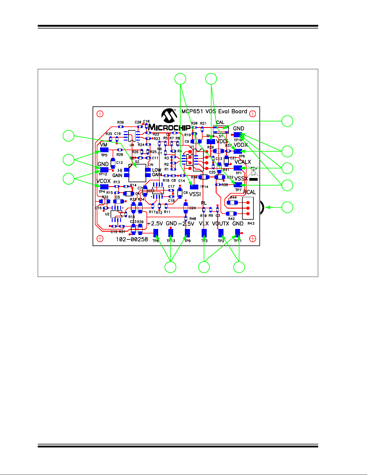
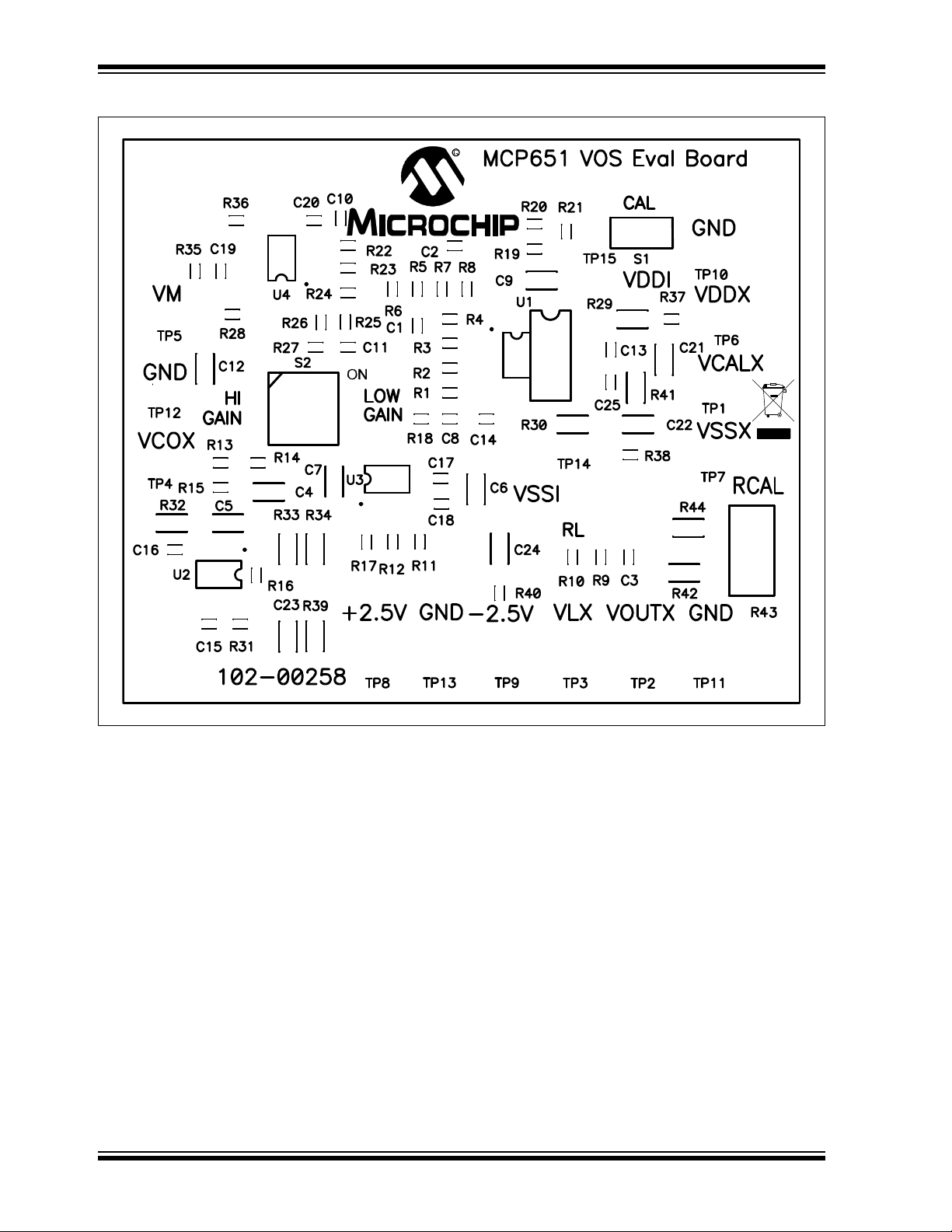
Lab equipment is connected to this board as shown in Figure 2-1. The (surface mount)
test points allow lab equipment to be connected to these boards.
FIGURE 2-1: Lab Equipment Connections and Configuration Switches for the MCP651 Input Offset
Evaluation Board.
The arrows and numbers in Figure 2-1 signify the following:
1. Gain Setting Switch – top position (# 1)
a) To the right (ON) for low gain (G
2. Voltmeter to measure VM
a) Gives amplified offset (G
b) To the left for high gain (G
3. Power Supply for VCOX
a) Can be left open (forces VOUTX = 0V).
M
AGMVOST
= 201 V/V).
M
=1998V/V).
).
b) Set between VSSI and VDDI.
4. ±2.5V Power Supplies with GND
a) Set at +2.5V and -2.5V (for best performance).
5. Power Supply for VLX (Load Resistor’s bias point)
a) Can be left open (fewer lab power supplies; R
b) Can be shorted to GND with a jumper wire (VLX = 0V and R
c) Can connect to an external lab power supply (R
=40kΩ).
L
=1kΩ).
L
=1kΩ).
L
DS51834A-page 12 © 2009 Microchip Technology Inc.
Page 17

Installation and Operation
6. Voltmeter to measure VOUTX
a) Typically not used (mainly used for validating DUT and board).
7. POT (RCAL) Thumb-wheel (to adjust VCALX)
a) Rotate clockwise (CW) to increase VCALX.
b) Rotate counter-clockwise (CCW) to decrease VCALX.
c) Usually set at mid-turn.
d) Can override with an external power supply at VCALX or a jumper wire (see
# 9 below)
8. Power Supply for VSSX
a) Minimum of about VDDX – (DUT’s maximum operating supply
voltage) – (0.12V for the resistors in the supply line).
b) Maximum of +0.3V (for V
c) When VSSX = -2.5V and VDDX = +2.5V, you can connect to the -2.5V
supply with a jumper wire (fewer lab power supplies).
9. Power Supply for VCALX
a) Usually not connected (RCAL sets V
b) Can be shorted to GND with a jumper wire (fewer lab power supplies;
V
CALX=VCMX
=0V).
c) Can connect to an external lab power supply (it is best, but not necessary, to
set RCAL to mid-supply).
10. Power Supply for VDDX
a) Minimum of -0.3V (for V
b) Maximum of about VSSX + (DUT’s maximum operating supply
voltage) + (0.12V for the resistors in the supply line).
c) When VSSX = -2.5V and VDDX = +2.5V, you can connect to the +2.5V
supply with a jumper wire (fewer lab power supplies).
11. CAL Switch
a) Press to initiate calibration sequence (corrects DUT’s V
common mode voltage set to VCALX).
b) There is a delay of about 4 ms for the calibration to complete, plus several
tenths of a second for the circuit to settle.
12. Voltmeter at VDDI and VDDX (to measure I
a) Measure ΔV=V
b) Calculate I
DDX–VDDI
= ΔV/(10Ω)
DD
13. Voltmeter at VSSI and VSSX (to measure I
a) Measure ΔV=V
b) Calculate I
SSX–VSSI
= ΔV/(10Ω); (this is a negative value)
SS
at 0.3V below negative rail).
CMX
; fewer lab power supplies).
CALX
at 0.3V above positive rail).
CMX
)
DD
.
)
SS
.
, with internal
OST
Note: For the best accuracy and ease of use, short VCALX to GND, set the other
voltages for the desired bias during calibration, then initiate a calibration
event in the DUT (push S1). Change the bias point afterwards to see how
V
is changed.
OST
© 2009 Microchip Technology Inc. DS51834A-page 13
Page 18

MCP651 Input Offset Evaluation Board User’s Guide
2.4 OPERATING CONDITIONS
The MCP651 Input Offset Evaluation Board works most effectively at room
temperature (near 25°C). Measurements at other temperatures should be done in an
oven where the air velocity is minimal. Table 2-1 shows the various DUT voltages (as
described in the data sheet), their nominal values and ranges, and how to convert to
the voltages needed on the MCP651 Input Offset Evaluation Board.
TABLE 2-1: CONVERTING VOLTAGES FOR THE BOARD
Single Supply Voltages (V)
Data Sheet
Symbol
V
DD
V
SS
V
CM
Nominal Range
2.5 or 5.5 2.5 to 5.5 V
00 V
VDD/3 VSS– 0.3 to VDD–1.3
0 ← VCM–V
(Note 1)
V
(Note 2) VDD/2 VSS+ 0.2 to VDD–0.2 V
OUT
V
L
V
CAL
CAL/CS V
VDD/2 VSS to V
DD
V
VDD/3 (Note 3) VSS+ 0.1 to VDD–1.4 V
SS
VSS to V
DD
(Note 4)
Note 1: At TA= +25°C. See the data sheet for changes in VCM range vs. TA.
2: Set the desired V
voltage at the V
OUT
input; the integrator then forces V
COX
be the same voltage.
3: When the V
connected, so V
4: The circuit forces CAL/CS
pin left open. However, this board always has the POT (R43)
CAL
is never truly open.
CALX
to stay within its range (as long as the supply voltages
are constant when the CAL switch is activated). Normally, the part is on.
5: These numbers are for the MCP651 op amp.
Once the MCP651 Input Offset Evaluation Board is powered up, the switches can be
set for the desired operation. S1 (a normally off push-button switch) starts a calibration
event (CAL), internal to the DUT, when pushed. S2 (top position) sets the gain of the
amplifier (G
) either high or low. See Table 2-2 for details.
M
Conversion
Equations (V)
← VDD–V
DDX
← VSS–V
SSX
← V
OUTX
← VL–V
LX
← V
CALX
CM
CM
CM
OUT–VCM
CM
CAL–VCM
OUT
to
TABLE 2-2: SWITCH OPERATION
Switch Input Result
S1 No Input Normal Operation
Pushed Calibration event started in DUT
S2 Top Switch to the left High Gain (1998 V/V)
Top Switch to the right Low Gain (201 V/V)
(Bottom Switch) (Don’t Care)
The gain is usually set low. It can be set high just after a calibration event, before
changing the DUT’s bias point, to obtain more accurate results for the calibrated offset
voltage.
The POT (R
or R43) adjusts V
CAL
. This voltage is where the DUT’s common mode
CALX
input voltage set during a calibration event (initiated by pushing S1). Adjusting this POT
does not have an effect on the circuit’s behavior until the CAL switch (S1) is pushed.
DS51834A-page 14 © 2009 Microchip Technology Inc.
Page 19

Installation and Operation
V
OST
VMGAG
M
()
⁄
=
Given:
Then:
V
OST
=0.5mV, VCM=0V
V
OST
=1.0mV, VCM=5V
ΔV
OST
=0.5mV
ΔVCM=5.0V
CMRR = 5.0V / 0.5 mV
=10V/mV
=80dB
2.5 CONVERTING TO OTHER PARAMETERS
2.5.1 Calculating DUT Parameters
The DUT’s total input offset voltage (V
) can be calculated from a measurement as
OST
shown in Equation 2-1.
EQUATION 2-1:
Changing the DUT’s bias voltages or ambient temperature changes V
application note AN1177 discusses in detail how these changes in V
. Microchip’s
OST
are related to
OST
specifications found in our data sheets. The following list summarizes the results:
• Specified Input Offset Voltage:
-V
= Input offset at the specified bias point
OS
• DC Common Mode Rejection Ratio:
- CMRR = ΔV
CM
/ΔV
OS
• DC Power Supply Rejection Ratio:
- PSRR = (ΔV
– ΔVSS)/ΔV
DD
OS
• DC Open-loop Gain:
-A
OL
= ΔV
OUT
/ΔV
OS
• Input Offset Drift over Temperature:
- ΔV
OS
/ΔT
A
Note: The data sheet Input Offset Voltage (VOS) specification applies to one bias
point and temperature only. The total input offset voltage (V
V
and changes in input offset as bias voltages and temperature change.
OS
) includes
OST
Example 2-1 gives an example of how V
voltage (V
CM
).
changes with the common mode input
OST
EXAMPLE 2-1: COMMON MODE CHANGE EXAMPLE
© 2009 Microchip Technology Inc. DS51834A-page 15
Page 20
MCP651 Input Offset Evaluation Board User’s Guide
2.5.2 Application
Table 2-3 shows one possible measurement matrix that will allow the user to estimate
key parameters for the DUT. Obviously, other values of V
selected.
TABLE 2-3: MEASUREMENT MATRIX
Operating Inputs Measurement (Note 1)
T
V
DD
(V)
V
(V)
A
(°C)
+25 5.5 2.75 1.83 40 V
0.20 1.83 V
5.30 V
2.5 1.25 0.83 V
0.20 0.83 V
2.30 V
-40 5.5 2.75 1.83 V
+85 V
+125 V
V
OUT
CM
(V)
-0.30 4 V
4.20 V
-0.30 V
1.20 V
G
M
(V/V)
Symbol Comments
VOS and PSRR
M1
CMRR
M2
CMRR
M3
A
M4
M5
M6
M7
M8
M9
M10
M11
M12
M13
OL
A
OL
VOS and PSRR
CMRR
CMRR
A
OL
A
OL
VOS at temperature and ΔVOS/ΔT
Note 1: Before making these measurements, set up the DUT to the bias point described for
. Short V
V
M1
, then alter the operating conditions for each succeeding measurement; do not
V
M1
to GND. Then start a calibration (CAL) event using S1. Measure
CALX
initiate another calibration event until all measurements are done.
Based on these measurements, we can make the following estimates, where the
V
values are calculated from the measured VMk values (see Equation 2-1):
OST_k
DD
and V
could be
CAL
A
TABLE 2-4: ESTIMATES
Operating Inputs Estimates
V
DD
(V)
1.8 and 5.5 +25 1/PSRR = (V
5.5 -40 V
1.8 +25 V
Obviously, other values of T
T
A
(°C)
OST_1–VOST_6
=V
OS
+25 VOS=V
+85 V
+125 V
OS
OS
-40 to +125 ΔVOS/ΔTA=(V
+25 1/CMRR = (V
1/AOL=(V
OS
1/CMRR = (V
1/A
OL
, VDD, … can be used instead, with the proper adjustments
A
OST_11
OST_1
=V
OST_12
=V
OST_13
OST_13–VOST_11
OST_3–VOST_2
OST_5–VOST_4
=V
OST_6
OST_8–VOST_7
=(V
OST_10–VOST_9
Equations Units
to these equations.
)/(3.0V) µV/V
µV
µV
µV
µV
) / (165°C) µV/°C
)/(4.5V) µV/V
)/(5.1V) µV/V
µV
)/(1.5V) µV/V
) / (2.1V) µV/V
DS51834A-page 16 © 2009 Microchip Technology Inc.
Page 21

Installation and Operation
2.6 SETTLING TIME, NOISE AND SAMPLING RATE
The bandwidth seen by the signal (DUT’s V
and noise voltage), between the DUT’s
OST
input and VM, is set mainly by the lowpass filter at the VM test point (TP5); this
bandwidth is about 1.6 Hz. This bandwidth sets the settling time seen at VM (after the
DUT’s bias point has been changed) to about 0.6 seconds.
The noise seen in the measurements is a result of DUT’s input noise voltage passed
through the same 1.6 Hz lowpass filter. The MCP651’s 1/f noise dominates at such low
frequencies, so V
will appear to wander over time. The standard deviation of this
OST
1/f wander can be estimated to be roughly:
•5µV
•34µV
for a time period of 1 second
P-P
for a time period of 10 years
P-P
Averaging several measurements together will help reduce the noise over a short
period of time. It must be understood, however, that the 1/f noise will make V
OST
appear to change over long periods of time.
There is a practical limit on increasing the sample rate; the noise does not improve
significantly after a certain point. The analog lowpass pole at 1.6 Hz causes closely
spaced samples to be correlated. To avoid the overhead caused by sampling too fast,
keep the sampling period near or above the pole’s time constant (0.10s); this gives a
minimum sample rate of 10 samples per second.
Note: Sampling much faster than 10 SPS will not improve the averaged noise
significantly.
© 2009 Microchip Technology Inc. DS51834A-page 17
Page 22

MCP651 Input Offset Evaluation Board User’s Guide
NOTES:
DS51834A-page 18 © 2009 Microchip Technology Inc.
Page 23

MCP651 INPUT OFFSET
V
OS
12.4 mV, Low Gain±
<
V
OS
1.25 mV, High Gain±
<
Where:
Low Gain = 201 V/V
High Gain = 1998 V/V
EVALUATION BOARD
USER’S GUIDE
Chapter 3. Possible Modifications
3.1 INTRODUCTION
This chapter shows how to modify the MCP651 Input Offset Evaluation Board to
measure other single op amps from Microchip Technology Inc. Items discussed in this
chapter include:
• Range of Parts Supported by the MCP651 Input Offset Evaluation Board
• Changes to Accommodate Other DUTs
3.2 RANGE OF PARTS SUPPORTED BY MCP651 INPUT OFFSET EVALUATION BOARD
Only op amps that fall within a certain performance range are supported by the
MCP651 Input Offset Evaluation Board.
3.2.1 Input Offset Voltage
In order to keep op amps U3 and U4 operating normally, the DUT’s VOS must be:
EQUATION 3-1:
More accurate op amps need higher gain for good resolution. Table 3-1 shows what
V
specs can be supported for different voltmeter resolutions and amplifier gains.
OS
TABLE 3-1: LOWER LIMIT ON V
Voltmeter Resolution
(mV)
1 mV 201 (low gain) 500
0.1 mV 201 (low gain) 50
Note 1: These results assume a minimum measurement resolution of 1% of the V
2: The DUT needs to be soldered to the PCB when the maximum V
±50 µV, or so. Inserting a PDIP-8 part into a 8-pin socket creates a contact potential
(error) of the order of ±1 µV. Also, 1/f noise needs to be low.
RANGE (NOTE 1)
OS
GAG
M
(V/V)
1998 (high gain) 50
1998 (high gain) 5 (Note 2)
max(VOS) ≥
(±µV)
OS
is less than
OST
range.
© 2009 Microchip Technology Inc. DS51834A-page 19
Page 24

MCP651 Input Offset Evaluation Board User’s Guide
V
OHVCM
– 7.5V
≤
VCMVOL– 7.5V
≤
500 kHz GBWP 100 MHz
≤≤
3.2.2 Output Headroom
The DUT’s output headroom needs to be close enough to 0V to not overdrive U2 or U3.
The maximum DUT V
EQUATION 3-2:
Rail-to-rail output op amps, on a single supply voltage, must be less than 7.5V.
3.2.3 Gain Bandwidth Product
There is a minimum Gain Bandwidth Product (GBWP) to keep the feedback loop
stable, and a maximum GBWP to avoid crosstalk and other issues.
EQUATION 3-3:
and VOL values supported (relative to VCM) are:
OH
DS51834A-page 20 © 2009 Microchip Technology Inc.
Page 25

Possible Modifications
MCP651
SOIC
VIN+
V
IN
–
V
SS
V
DD
V
OUT
1
2
3
4
8
7
6
5
V
CAL
CAL/CSNC
DUT in PDIP-8DUT in SOIC-8
3.3 CHANGES TO ACCOMMODATE OTHER DUTS
This section focuses on methods to connect to other DUTs; the circuit’s design is not
changed. Parts information can be found in Appendix B. “Bill Of Materials (BOM)”.
3.3.1 Pinout
Figure 3-1 shows the MCP651 op amp’s pinout. This is the standard 8-lead pinout,
except for pins 5 and 8 (V
Board is designed to take advantage of these input pins, but they are not necessary to
this board’s operation.
FIGURE 3-1: MCP651 Pinout.
Op Amps with No Connection (NC) at pins 1, 5 and 8 will operate properly on the
MCP651 Input Offset Evaluation Board. Other op amps may need to use an adaptor
board; see Section 3.3.5 “Other Single Op Amps”.
and CAL/CS). The MCP651 Input Offset Evaluation
CAL
3.3.2 Removing the DUT
Since these boards come with the DUT (in SOIC-8) soldered on, it is necessary to
de-solder them. Figure 3-2 shows the location of the DUT for either a SOIC-8 or a
PDIP-8 package. A good de-soldering station makes this work much easier to do.
FIGURE 3-2: DUT’s Location on the PCB.
© 2009 Microchip Technology Inc. DS51834A-page 21
Page 26

MCP651 Input Offset Evaluation Board User’s Guide
3.3.3 Single Op Amps in SOIC-8 Package
Solder onto the SOIC-8 pad shown in Figure 3-2. Pin 1 is on the top left (next to the U1
label). To avoid soldering and de-soldering many times, for slower parts, it may be
better to use the option discussed in Section 3.3.5 “Other Single Op Amps”.
3.3.4 Single Op Amps in PDIP-8 Package
Remove the original SOIC-8 packaged part. Solder a DIP-8 IC Socket in the PDIP-8
location shown on Figure 3-2; this makes it easy to change PDIP-8 parts. It also is
helpful for parts for other package and pinout options; see Section 3.3.5 “Other
Single Op Amps”. Figure 3-3 shows this board after the DIP-8 IC socket has been
installed.
FIGURE 3-3: PCB with SOIC-8 Part Removed and DIP-8 IC Socket Installed.
The socket may not work well in two cases (solder directly to the PCB instead):
• Very fast op amps (i.e., GBWP > 100 MHz)
• Very accurate op amps (i.e., V
<±50µV)
OST
3.3.5 Other Single Op Amps
With a DIP-8 IC Socket on the evaluation board (see Section 3.3.4 “Single Op Amps
in PDIP-8 Package”), it is relatively easy to adapt the MCP651 Input Offset Evaluation
Board to many other op amps. An adaptor board is stacked on top using headers that
solder to the adaptor board, using PDIP-8 through holes, and are inserted into the
DIP-8 socket on the evaluation board. The adaptor board can accommodate:
• Different packages
• Different pinout options (can be dealt with on the adaptor board)
• Parts with multiple op amps
The adaptor boards approach may not work well in two cases:
• Fast op amps (i.e., GBWP > 10 MHz); adding bypass capacitors to the adaptor
board may help
• Accurate op amps (i.e., V
DS51834A-page 22 © 2009 Microchip Technology Inc.
<±50µV)
OST
Page 27

Possible Modifications
Front
View
Back
View
Figure 3-4 shows a SOIC-8 op amp soldered onto the 8-Pin SOIC/MSOP/TSSOP/DIP
Evaluation Board available from Microchip Technology Inc. The two interconnect strips
on the bottom are soldered into the through holes for the DIP-8 socket. Figure 3-5
shows this board plugged into the MCP651 Input Offset Evaluation Board.
Note 1: Build the adaptor board in the following sequence. Insert the interconnect
headers into the DIP-8 socket on the MCP651 Input Offset Evaluation
Board. Place the SOIC8EV board on the top of the interconnect headers,
while maintaining the correct pin orientation. Solder the headers to the
top board. Clip the pins flush with the top surface of the SOIC8EV board,
then solder the (SOIC-8) op amp on the top.
2: See Table B-4 for part numbers of this board and its components.
FIGURE 3-4: Op Amp in SOIC-8 Package and Connector Headers Soldered to
Adaptor PCB.
FIGURE 3-5: Adaptor Board Connected to the MCP651 Input Offset Evaluation
Board.
© 2009 Microchip Technology Inc. DS51834A-page 23
Page 28

MCP651 Input Offset Evaluation Board User’s Guide
NOTES:
DS51834A-page 24 © 2009 Microchip Technology Inc.
Page 29

Appendix A. Schematics and Layouts
A.1 INTRODUCTION
This appendix contains the schematics and layouts for the MCP651 Input Offset
Evaluation Board.
A.2 SCHEMATIC AND LAYOUTS
See A.3 “Board – Schematic” for the circuit diagram. U1 is the DUT (MCP651). U2
buffers the attenuated and filtered control voltage VCOX. U3 is the differential
integrator. U4 is the amplifier that gives the final gain to the DUT’s input offset voltage
(V
). Switch S1 gives the user a means of starting an auto-calibration cycle in the
OST
DUT. Switch S2 makes it so the amplifier (U4) can have two different gains, providing
a tradeoff between accuracy and range.
A.4 “Board – Combination of the Top Silk-Screen, Top Solder Mask and Top Metal
Layers” through A.7 “Board – Bottom Metal Layer” show the PCB layout plots. This
PCB has two metal layers: signal and power traces on top and ground plane on bottom.
Groups of critical resistors have been arranged so that their thermoelectric voltages
cancel (assuming constant temperature gradient); these groups are:
•R
through R
1
•R5 and R
•R7 and R
•R21 through R
•R24 and R
The Gerber files for this board are available on the Microchip website
(www.microchip.com) and are contained in the zip file “00258R2_Gerbers.zip”.
4
6
8
23
25
MCP651 INPUT OFFSET
EVALUATION BOARD
USER’S GUIDE
© 2009 Microchip Technology Inc. DS51834A-page 25
Page 30

MCP651 Input Offset Evaluation Board User’s Guide
M
A.3 BOARD – SCHEMATIC
DS51834A-page 26 © 2009 Microchip Technology Inc.
Page 31

Schematics and Layouts
A.4 BOARD – COMBINATION OF THE TOP SILK-SCREEN, TOP SOLDER MASK
AND TOP METAL LAYERS
© 2009 Microchip Technology Inc. DS51834A-page 27
Page 32
MCP651 Input Offset Evaluation Board User’s Guide
A.5 BOARD – TOP SILK-SCREEN
DS51834A-page 28 © 2009 Microchip Technology Inc.
Page 33
Schematics and Layouts
A.6 BOARD – TOP SOLDER MASK AND TOP METAL LAYER
© 2009 Microchip Technology Inc. DS51834A-page 29
Page 34
MCP651 Input Offset Evaluation Board User’s Guide
A.7 BOARD – BOTTOM METAL LAYER
DS51834A-page 30 © 2009 Microchip Technology Inc.
Page 35
MCP651 INPUT OFFSET
EVALUATION BOARD
USER’S GUIDE
Appendix B. Bill Of Materials (BOM)
B.1 MCP651 INPUT OFFSET EVALUATION BOARD BOM
The BOM in Table B-1 shows all of the components assembled on the PCB. Table B-2
shows alternate components that can be placed on this PCB (after modification).
Table B-3 shows components that are not populated.
TABLE B-1: BILL OF MATERIALS FOR ASSEMBLED PCB
Qty
1 C8 1.0 nF, 0603 SMD, X7R, 16V, 10% Panasonic
1 C2 22 nF, 0603 SMD, X7R, 16V, 10% Panasonic-ECG ECJ-1VB1C223K
1 C10 33 nF, 0603 SMD, X7R, 16V, 10% Panasonic-ECG ECJ-1VB1C333K
11 C3, C11,
2 C6, C7 150 nF, 1206 SMD, X7R, 50V, 10% Panasonic-ECG ECJ-3VB1C154K
4 C4, C5, C9, C12 1.0 µF, 1206 SMD, X7R, 16V, 10% Panasonic-ECG ECJ-3YB1C105K
4 C21 – C24 10 µF, 1206 SMD, X7R, 16V, 10% Panasonic-ECG ECJ-3YX1C106K
1 PCB MCP651 Input Offset Evaluation Board,
2 R2, R3 200Ω, 0603 SMD, 0.1%, 25 ppm/°C, 1/10W Susumu Co. Ltd. RG1608P-201-B-T5
1 R23 5.10 kΩ, 0603 SMD, 0.1%, 25 ppm/°C, 1/10W Susumu Co. Ltd. RG1608P-512-B-T5
1 R4 10.0 kΩ, 0603 SMD, 0.1%, 25 ppm/°C, 1/10W Susumu Co. Ltd. RG1608P-103-B-T5
1 R24 15.0 kΩ, 0603 SMD, 0.1%, 25 ppm/°C, 1/10W Susumu Co. Ltd. RG1608P-153-B-T5
1 R26 86.6 kΩ, 0603 SMD, 0.1%, 25 ppm/°C, 1/10W Susumu Co. Ltd. RG1608P-8662-B-T5
1 R25 93.1 kΩ, 0603 SMD, 0.1%, 25 ppm/°C, 1/10W Susumu Co. Ltd. RG1608P-9312-B-T5
2 R12, R14 150 kΩ, 0603 SMD, 0.1%, 25 ppm/°C, 1/10W Susumu Co. Ltd. RG1608P-154-B-T5
2 R11, R13 332 kΩ, 0603 SMD, 0.1%, 25 ppm/°C, 1/10W Susumu Co. Ltd. RG1608P-3323-B-T5
2 R37, R38 4.99Ω, 0603 SMD, 1%, 1/10W Yageo RC0603FR-074R99L
1 R10 1.00 kΩ, 0603 SMD, 1%, 1/10W Panasonic-ECG ERJ-3EKF1001V
2 R5, R6 4.02 kΩ, 0603 SMD, 1%, 1/10W Panasonic-ECG ERJ-3EKF4021V
1 R22 4.99 kΩ, 0603 SMD, 1%, 1/10W Panasonic-ECG ERJ-3EKF4991V
2 R7, R8 20.0 kΩ, 0603 SMD, 1%, 1/10W Panasonic-ECG ERJ-3EKF2002V
1 R17 102 kΩ, 0603 SMD, 1%, 1/10W Panasonic-ECG ERJ-3EKF1023V
4 R31, R35, R36,
1 R27 100Ω, 0603 SMD, 5%, 1/10W Panasonic-ECG ERJ-3GEYJ101V
2 R16, R18 3.3 kΩ, 0603 SMD, 5%, 1/10W Panasonic-ECG ERJ-3GEYJ332V
4 R1, R9, R19, R21 10 kΩ, 0603 SMD, 5%, 1/10W Panasonic-ECG ERJ-3GEYJ103V
3 R15, R20, R28 100 kΩ, 0603 SMD, 5%, 1/10W Panasonic-ECG ERJ-3GEYJ104V
2 R29, R30 4.99Ω, 1206 SMD, 1%, 1/4W Yageo RC1206FR-074R99L
Note 1: The components listed in this Bill of Materials are representative of the PCB assembly. The released BOM
Reference
Designator
100 nF, 0603 SMD, X7R, 16V, 10% Panasonic-ECG ECJ-1VB1C104K
C13–C20, C25
2-layer PCB (3.00 in × 2.50 in)
10Ω, 0603 SMD, 5%, 1/10W Panasonic-ECG ERJ-3GEYJ100V
R40
used in manufacturing uses all RoHS-compliant components.
Description Manufacturer Part Number
®
-ECG ECJ-1VB1H102K
Microchip
Technology Inc.
102-00258
© 2009 Microchip Technology Inc. DS51834A-page 31
Page 36
Bill Of Materials (BOM)
Qty
5 R32 – R34, R39,
1 R42 150Ω, 1206 SMD, 5%, 1/4W Panasonic-ECG ERJ-8GEYJ151V
1 R44 2.2 kΩ, 1206 SMD, 5%, 1/4W Panasonic-ECG ERJ-8GEYJ222V
1 R43 10 kΩ POT, SMD, 20%, 1 Turn Thumbwheel Bournes Inc. 3352T-1-103LF
1 S1 SPST-NO, SMD, Switch, Push Button, 1 Pos. Panasonic-ECG EVQ-P2R02M
1 S2 SMD, Switch, DIP, 2 Pos. Grayhill Inc. 90HBW02PT
15 TP1 – TP15 SMD, Test Point Keystone
1 U1 SOIC-8, Single Op Amp Microchip
3 U2 – U4 MCP6V01, SOIC-8, Single Op Amp MCP6V01-E/SN
4 (for PCB mounting) Hemispherical Bumpon Standoff,
Note 1: The components listed in this Bill of Materials are representative of the PCB assembly. The released BOM
Reference
Designator
10Ω, 1206 SMD, 5%, 1/4W Panasonic-ECG ERJ-8GEYJ100V
R41
0.44 in × 0.20 in
used in manufacturing uses all RoHS-compliant components.
Description Manufacturer Part Number
Electronics
Technology Inc.
3M SJ-5003 (BLACK)
®
5016
MCP651-E/SN
TABLE B-2: BILL OF MATERIALS FOR ALTERNATE COMPONENTS
Qty
0 U1 PDIP-8, Single Op Amp Microchip
0 U1 DIP-8 IC Socket Tyco
0 (for PCB mounting) Stand-off, Hex, 0.500", 4 × 40 Thread, Nylon,
0 (for PCB mounting) Machine Screw, Phillips, 4 × 40 Thread,
Note 1: The MCP6XXX represents any Microchip single op amp, with standard pinout, that fits the given design.
Reference
Designator
0.285" max. O.D.
1/4" long, Nylon
2: The components listed in this Bill of Materials are representative of the PCB assembly. The released BOM
used in manufacturing uses all RoHS-compliant components.
Description Manufacturer Part Number
MCP6XXX (Note 1)
Technology Inc.
2-641260-1
Electronics
Keystone
Electronics
Building
Fasteners
1902C
NY PMS 440 0025 PH
TABLE B-3: BILL OF MATERIALS FOR NOT POPULATED COMPONENTS
Qty
0 C1 Unknown Value, 0603 SMD, X7R, 16V, 10% Panasonic
Note 1: The components listed in this Bill of Materials are representative of the PCB assembly. The released BOM
© 2009 Microchip Technology Inc. DS51834A-page 32
Reference
Designator
used in manufacturing uses all RoHS-compliant components.
Description Manufacturer Part Number
®
-ECG —
Page 37

Bill Of Materials (BOM)
B.2 ADAPTOR BOARD BOM
The BOM in Table B-4 shows the components needed to build the adaptor board for
alternate DUT’s (see Figure 3-4).
TABLE B-4: BILL OF MATERIALS FOR ADAPTOR BOARD
Reference
Qty
Designator
1 — 8-Pin SOIC/MSOP/TSSOP/DIP Evaluation Board Microchip Technology
2 — Board-to-Board Connector, Low Profile Header,
4 Positions, 0.100 in, Gold Plated
2 — 100 nF, 0603 SMD, X7R, 16V, 10% Panasonic
1 — Single Op Amp in Standard 8-pin pinout Microchip Technology
Note 1: The components listed in this Bill of Materials are representative of the PCB assembly. The released BOM
used in manufacturing uses all RoHS-compliant components.
Description Manufacturer Part Number
SOIC8EV
Inc.
Samtec Inc. BBL-104-G-F
®
-ECG ECJ-1VB1C104K
MCP6XXX
Inc.
© 2009 Microchip Technology Inc. DS51834A-page 33
Page 38

WORLDWIDE SALES AND SERVICE
AMERICAS
Corporate Office
2355 West Chandler Blvd.
Chandler, AZ 85224-6199
Tel: 480-792-7200
Fax: 480-792-7277
Technical Support:
http://support.microchip.com
Web Address:
www.microchip.com
Atlanta
Duluth, GA
Tel: 678-957-9614
Fax: 678-957-1455
Boston
Westborough, MA
Tel: 774-760-0087
Fax: 774-760-0088
Chicago
Itasca, IL
Tel: 630-285-0071
Fax: 630-285-0075
Cleveland
Independence, OH
Tel: 216-447-0464
Fax: 216-447-0643
Dallas
Addison, TX
Tel: 972-818-7423
Fax: 972-818-2924
Detroit
Farmington Hills, MI
Tel: 248-538-2250
Fax: 248-538-2260
Kokomo
Kokomo, IN
Tel: 765-864-8360
Fax: 765-864-8387
Los Angeles
Mission Viejo, CA
Tel: 949-462-9523
Fax: 949-462-9608
Santa Clara
Santa Clara, CA
Tel: 408-961-6444
Fax: 408-961-6445
Toronto
Mississauga, Ontario,
Canada
Tel: 905-673-0699
Fax: 905-673-6509
ASIA/PACIFIC
Asia Pacific Office
Suites 3707-14, 37th Floor
Tower 6, The Gateway
Harbour City, Kowloon
Hong Kong
Tel: 852-2401-1200
Fax: 852-2401-3431
Australia - Sydney
Tel: 61-2-9868-6733
Fax: 61-2-9868-6755
China - Beijing
Tel: 86-10-8528-2100
Fax: 86-10-8528-2104
China - Chengdu
Tel: 86-28-8665-5511
Fax: 86-28-8665-7889
China - Hong Kong SAR
Tel: 852-2401-1200
Fax: 852-2401-3431
China - Nanjing
Tel: 86-25-8473-2460
Fax: 86-25-8473-2470
China - Qingdao
Tel: 86-532-8502-7355
Fax: 86-532-8502-7205
China - Shanghai
Tel: 86-21-5407-5533
Fax: 86-21-5407-5066
China - Shenyang
Tel: 86-24-2334-2829
Fax: 86-24-2334-2393
China - Shenzhen
Tel: 86-755-8203-2660
Fax: 86-755-8203-1760
China - Wuhan
Tel: 86-27-5980-5300
Fax: 86-27-5980-5118
China - Xiamen
Tel: 86-592-2388138
Fax: 86-592-2388130
China - Xian
Tel: 86-29-8833-7252
Fax: 86-29-8833-7256
China - Zhuhai
Tel: 86-756-3210040
Fax: 86-756-3210049
ASIA/PACIFIC
India - Bangalore
Tel: 91-80-3090-4444
Fax: 91-80-3090-4080
India - New Delhi
Tel: 91-11-4160-8631
Fax: 91-11-4160-8632
India - Pune
Tel: 91-20-2566-1512
Fax: 91-20-2566-1513
Japan - Yokohama
Tel: 81-45-471- 6166
Fax: 81-45-471-6122
Korea - Daegu
Tel: 82-53-744-4301
Fax: 82-53-744-4302
Korea - Seoul
Tel: 82-2-554-7200
Fax: 82-2-558-5932 or
82-2-558-5934
Malaysia - Kuala Lumpur
Tel: 60-3-6201-9857
Fax: 60-3-6201-9859
Malaysia - Penang
Tel: 60-4-227-8870
Fax: 60-4-227-4068
Philippines - Manila
Tel: 63-2-634-9065
Fax: 63-2-634-9069
Singapore
Tel: 65-6334-8870
Fax: 65-6334-8850
Taiwan - Hsin Chu
Tel: 886-3-6578-300
Fax: 886-3-6578-370
Taiwan - Kaohsiung
Tel: 886-7-536-4818
Fax: 886-7-536-4803
Taiwan - Taipei
Tel: 886-2-2500-6610
Fax: 886-2-2508-0102
Thailand - Bangkok
Tel: 66-2-694-1351
Fax: 66-2-694-1350
EUROPE
Austria - Wels
Tel: 43-7242-2244-39
Fax: 43-7242-2244-393
Denmark - Copenhagen
Tel: 45-4450-2828
Fax: 45-4485-2829
France - Paris
Tel: 33-1-69-53-63-20
Fax: 33-1-69-30-90-79
Germany - Munich
Tel: 49-89-627-144-0
Fax: 49-89-627-144-44
Italy - Milan
Tel: 39-0331-742611
Fax: 39-0331-466781
Netherlands - Drunen
Tel: 31-416-690399
Fax: 31-416-690340
Spain - Madrid
Tel: 34-91-708-08-90
Fax: 34-91-708-08-91
UK - Wokingham
Tel: 44-118-921-5869
Fax: 44-118-921-5820
03/26/09
DS51834A-page 34 © 2009 Microchip Technology Inc.
 Loading...