

Page 1
MCP47X6
PICtail™ Plus
Daughter Board
User’s Guide
© 2011 Microchip Technology Inc. DS51932B
Page 2
Note the following details of the code protection feature on Microchip devices:
• Microchip products meet the specification contained in their particular Microchip Data Sheet.
• Microchip believes that its family of products is one of the most secure families of its kind on the market today, when used in the
intended manner and under normal conditions.
• There are dishonest and possibly illegal methods used to breach the code protection feature. All of these methods, to our
knowledge, require using the Microchip products in a manner outside the operating specifications contained in Microchip’s Data
Sheets. Most likely, the person doing so is engaged in theft of intellectual property.
• Microchip is willing to work with the customer who is concerned about the integrity of their code.
• Neither Microchip nor any other semiconductor manufacturer can guarantee the security of their code. Code protection does not
mean that we are guaranteeing the product as “unbreakable.”
Code protection is constantly evolving. We at Microchip are committed to continuously improving the code protection features of our
products. Attempts to break Microchip’s code protection feature may be a violation of the Digital Millennium Copyright Act. If such acts
allow unauthorized access to your software or other copyrighted work, you may have a right to sue for relief under that Act.
Information contained in this publication regarding device
applications and t he lik e is provided only for your convenience
and may be su perseded by upda t es . It is y our responsibility to
ensure that your application meets with your specifications.
MICROCHIP MAKES NO REPRESENTATIONS OR
WARRANTIES OF ANY KIND WHETHER EXPRESS OR
IMPLIED, WRITTEN OR ORAL, STATUTORY OR
OTHERWISE, RELATED TO THE INFORMATION,
INCLUDING BUT NOT LIMITED TO ITS CONDITION,
QUALITY, PERFORMANCE, MERCHANTABILITY OR
FITNESS FOR PURPOSE. Microchip disclaims all liability
arising from this information and its use. Use of Microchip
devices in life supp ort and/or safety ap plications is entir ely at
the buyer’s risk, and the buyer agrees to defend, indemnify and
hold harmless M icrochip from any and all dama ges, claims,
suits, or expenses re sulting from such use. No licens es are
conveyed, implicitly or otherwise, under any Microchip
intellectual property rights.
Trademarks
The Microchip name and logo, the Microchip logo, dsPIC,
K
EELOQ, KEELOQ logo, MPLAB, PIC, PICmicro, PICSTART,
32
PIC
logo, rfPIC and UNI/O are registered trademarks of
Microchip Technology Incorporated in the U.S.A. and other
countries.
FilterLab, Hampshire, HI-TECH C, Linear Active Thermistor,
MXDEV, MXLAB, SEEVAL and The Embedded Control
Solutions Company are registered trademarks of Microchip
Technology Incorporated in the U.S.A.
Analog-for-the-Digital Age, Application Maestro, chipKIT,
chipKIT logo, CodeGuard, dsPICDEM, dsPICDEM.net,
dsPICworks, dsSPEAK, ECAN, ECONOMONITOR,
FanSense, HI-TIDE, In-Circuit Serial Programming, ICSP,
Mindi, MiWi, MPASM, MPLAB Certified logo, MPLIB,
MPLINK, mTouch, Omniscient Code Generation, PICC,
PICC-18, PICDEM, PICDEM.net, PICkit, PICtail, REAL ICE,
rfLAB, Select Mode, Total Endurance, TSHARC,
UniWinDriver, WiperLock and ZENA are trademarks of
Microchip Technology Incorporated in the U.S.A. and other
countries.
SQTP is a service mark of Microchip Technology Incorporated
in the U.S.A.
All other trademarks mentioned herein are property of their
respective companies.
© 2011, Microchip Technology Incorporated, Printed in the
U.S.A., All Rights Reserved.
Printed on recycled paper.
ISBN: 978-1-61341-709-6
Microchip received ISO/TS-16949:2009 certification for its worldwide
headquarters, design and wafer fabrication facilities in Chandler and
Tempe, Arizona; Gresham, Oregon and design centers in California
and India. The Company’s quality system processes and procedures
are for its PIC
devices, Serial EEPROMs, microperipherals, nonvolatile memory and
analog products. In addition, Microchip’s quality system for the design
and manufacture of development systems is ISO 9001:2000 certified.
®
MCUs and dsPIC® DSCs, KEELOQ
®
code hopping
DS51932B-page 2 © 2011 Microchip Technology Inc.
Page 3

MCP47X6 PICtail™ PLUS DAUGHTER
BOARD USER’S GUIDE
Table of Contents
Preface ...........................................................................................................................5
Introduction............................................................................................................5
Document Layout .................................................................................................. 5
Conventions Used in this Guide............................................................................ 6
Recommended Reading.............................................................. .. ........................7
The Microchip Web Site........................................................................................ 7
Customer Support.................... .................................... .................. .......................7
Document Revision History................................................................................... 8
Chapter 1. Quick Start Instructions
1.1 Introduction .....................................................................................................9
1.2 Description of the MCP47X6 PICtail™ Plus Daughter Board ........................9
1.3 I2C Address B y te fo r E a ch D e v ice ............................................................... 11
1.4 Getting Started With the Explorer 16 Development Board ........................... 12
1.5 Connecti n g to the E xp l o re r 1 6 St a rt er Ki t ............... .. .................................... 13
1.6 Getting Started with PICkit™ Serial Analyzer .............................................. 20
1.7 Examples for Other Devices (MCP4706, MCP4716) ...................................30
1.8 Programming Example using the PICkit™ Serial Analyzer ..........................31
Appendix A. Schematic and Layouts
A.1 Introduction ..................................................................................................33
A.2 Board – Schematic ... .................................................................... ................ 3 4
A.3 Board – Top Silk and Pads ..........................................................................35
A.4 Board – Top Copper, Top Pads and Top Silk ................ .......................... .. ..36
A.5 Board – Bottom Silk and Pads ................ .......................... .. ........................37
A.6 Board – Bottom Copper, Bottom Pads and Silk .............................. .............38
Appendix B. Bill Of Materials (BOM)
Worldwide Sales and Service ....................................................................................40
© 2011 Microchip Technology Inc. DS51932B-page 3
Page 4

MCP47X6 PICtail™ Plus Daughter Board User’s Guide
DS51932B-page 4 © 2011 Microchip Technology Inc.
Page 5
MCP47X6 PICtail™ PLUS DAUGHTER
BOARD USER’S GUIDE
Preface
NOTICE TO CUSTOMERS
All documentation becomes dated, and this manual is no exception. Microchip tools and
documentation are constantly evolving to meet customer needs, so some actual dialogs
and/or tool descriptions may differ from those in this document. Please refer to our web site
(www.microchip.com) to obtain the latest documentation available.
Documents are identified with a “DS” number. This number is located on the bottom of each
page, in front of the p age number. The numbering convention for the DS number is
“DSXXXXXA”, where “XXXXX” is the document number and “A” is the revision level of the
document.
For the most up-to-date information on development tools, see the MPLAB
Select the Help menu, and then Topics to open a list of available online help files.
®
IDE online help.
INTRODUCTION
This chapter contains general information that will be useful to know before using the
MCP47X6 PICtail™ Plus Daughter Board. Items discussed in this chapter include:
• Document Layout
• Conventions Used in this Guide
• Recommended Reading
• The Microchip Web Site
• Customer Support
• Document Revision History
DOCUMENT LAYOUT
This document describes how to use the MCP47X6 PICtail™ Plus Daughter Board as
a development tool to emulate and debug firmware on a target board. The manual layout is as follows:
• Chapter 1. “Quick Start Instructions” – this chapter provides an overview of the
MCP47X6 PICtail™ Plus Daughter Board and instructions on how to program the
DAC register and EEPROM of the MCP4706/MCP4716/MCP4726 devices.
• Appendix A. “Schematic and Layouts” – shows the schematic and layout
diagrams for the MCP47X6 PICtail™ Plus Daughter Board.
• Appendix B. “Bill Of Materials (BOM)” – lists the parts used to build the
MCP47X6 PICtail™ Plus Daughter Board.
© 2011 Microchip Technology Inc. DS51932B-page 5
Page 6
MCP47X6 PICtail™ Plus Daughter Board User’s Guide
CONVENTIONS USED IN THIS GUIDE
This manual uses the following docum entat io n conven tion s:
DOCUMENTATION CONVENTIONS
Description Represents Examples
Arial font:
Italic chara c ters Referenced books MPLAB
Emphasized text ...is the only compiler...
Initial caps A window the Output window
A dialog the Settings dialog
A menu selection select Enable Programmer
Quotes A field name in a window or
dialog
Underlined, italic text with
right angle bracket
Bold characters A dialog button Click OK
N‘Rnnnn A number in verilog format,
Text in angle brac kets < > A key on the keyboard Press <Enter>, <F1>
Courier New font:
Plain Courier New Sample source code #define START
Italic Courier New A variable argument file.o, where file can be
Square brackets [ ] Optional arguments mcc18 [options] file
Curly brackets and pipe
character: { | }
Ellipses... Replaces r epeated text var_name [,
A menu path File>Save
A tab Click the Power tab
where N is the tota l number of
digits, R is th e radi x and n is a
digit.
Filenames autoexec.bat
File paths c:\mcc18\h
Keywords _asm, _endasm, static
Command-line options -Opa+, -Opa-
Bit values 0, 1
Constants 0xFF, ‘A’
Choice of mut ually exclus ive
arguments; an OR selection
Represents code supplied by
user
“Save project before build”
4‘b0010, 2‘hF1
any valid filename
[options]
errorlevel {0|1}
var_name...]
void main (void)
{ ...
}
®
IDE User’s Guide
DS51932B-page 6 © 2011 Microchip Technology Inc.
Page 7

RECOMMENDED READING
This user's guide describes how to use MCP47X6 PICtail™ Plus Daughter Board. The
following Microchip documents are available and recommended as supplemental
reference resources.
PICkit™ Serial Analyzer User’s Guide (DS51647)
Consult this document for instr ucti ons on how to use the PICkit™ Serial Analyzer
hardware and software.
MCP4706/MCP4716/MCP 472 6 Data Sheet, “8-/10- /12 -Bi t Voltage Output
Digital-to-Analog Converter with EEPROM Memory” (DS22272)
This data sheet provides deta iled information regarding the MCP47x6 product family.
PIC24FJ128GA010 Family Data Sheet (DS39747)
Explorer 16 Development Board User’s Guide (DS51589)
AN1079, “Using the C30 Compiler and the I2C Peripheral to Interface Serial
EEPROMs with dsPIC33F” (DS01079)
THE MICROCHIP WEB SITE
Microchip provides online support via our web site at www.microchip.com. This web
site is used as a means to make files and information easily available to customers.
Accessible by using your favorite Internet browser, the web site contains the following
information:
• Product Support – Data sheets and errata, application notes and sample
programs, design resources, user’s guides and hardware support documents,
latest software releases and archived software
• General Technical Support – Frequently Asked Questions (FAQs), technical
support requests, online discussion groups, Microchip consultant program
member listing
• Business of Microchip – Product selector and ordering guides, latest Microchip
press releases, listing of seminars and events, listings of Microchip sales offices,
distributors and factory representatives
Preface
CUSTOMER SUPPORT
Users of Microchip products can receive assistance through several channels:
• Distributor or Representative
• Local Sales Office
• Field Application Engineer (FAE)
• Technical Support
Customers should contact their distributor, representative or field application engineer
(FAE) for support. Local sales offices are also available to help customers. A listing of
sales offices and locations is included in the back of this document.
Technical support is available through the web site at: http://support.microchip.com.
© 2011 Microchip Technology Inc. DS51932 B-page 7
Page 8

MCP47X6 PICtail™ Plus Daughter Board User’s Guide
DOCUMENT REVISION HISTORY
Revision B (October 2011)
• Replaced the front and back views of the board with updated photos for Figure
1-1: “Front and Back Views of the MCP47X6 PICtail™ Plus Daughter Board.”
• Added buzzer information to Appendix B. “Bill Of Materials (BOM)”.
Revision A (May 201 1)
• Initial Release of this Document.
DS51932B-page 8 © 2011 Microchip Technology Inc.
Page 9
Chapter 1. Quick Start Instructions
1.1 INTRODUCTION
The following sections provide an overview of the MCP47X6 PICtail™ Plus Daughter
Board and demonstrate how to: (a) use these devices in a 16-bit MCU environment and
(b) evaluate these device’s features using the PICkit™ Serial Analyzer (P/N:
DV164122). The MCP47X6 PICtail™ Plus Daughter Board is designed to work with
both the Explorer 16 Development Board (P/N: DV164033) and the PICkit
Analyzer (P/N: DV164122).
The following topics are covered:
• Description of the MCP47X6 PICtail™ Plus Daughter Board.
• How to use the MCP47X6 PICtail™ Plus Daughter Board with the Explorer 16
Starter Kit.
• How to use MCP47X6 PICtail™ Plus Daughter Board with the PICkit
Analyzer.
MCP47X6 PICtail™ PLUS DAUGHTER
BOARD USER’S GUIDE
™
Serial
™
Serial
Note 1: If you use the PIC Explorer 16, you need Sections 1.4
™
2: If y ou us e th e PIC kit
Serial Analyzer, you need Sections 1.6 — 1.8 only.
— 1.5 only.
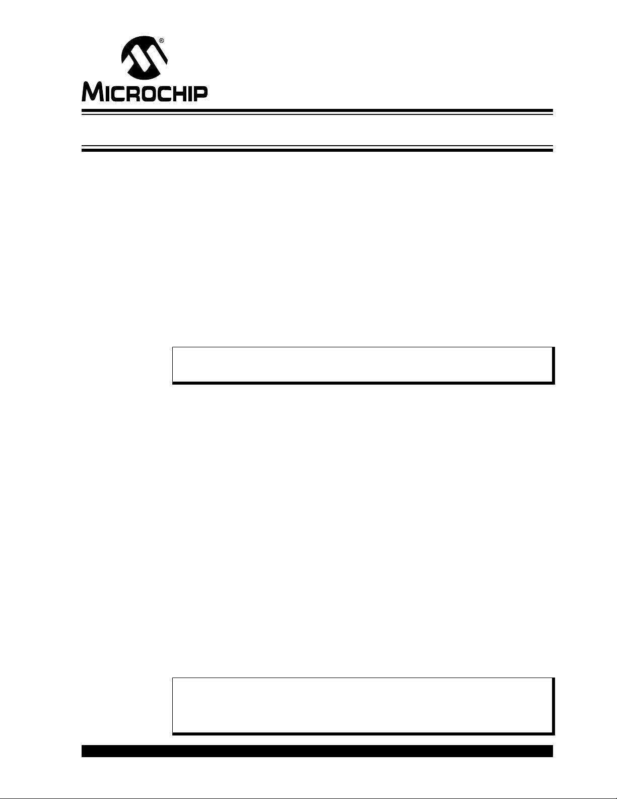
1.2 DESCRIPTION OF THE MCP47X6 PICtail™ PLUS DAUGHTER BOARD
The MCP47X6 PICtail™ Plus Daughter Board (P/N ADM00317) contains the
MCP4706 (8-bit DAC), MCP4716 (10-bit DAC), and MCP4726 (12-bit DAC) devices.
These DAC devices are communicating with the external Master device (MCU) using
2
I
C serial interface communication. The MCP47X6 PICtail™ Plus Daughter Board
does not include the Master device (MCU), but it has two interface connectors that can
be used for the external device, which has the Master device (MCU) to communicate
with this board. The two interfaces are:
(a) Connector (J3) for Explorer 16 Starter Kit (P/N: DV164033) for 16-bit MCU
environment. The firmware for the 16-bit MCU is provided with this board.
(b) 6-pin connector (J1) for PICkit™ Serial Analyzer (P/N: DV164122) for reading and
writing the DAC registers using the PICkit™ Serial Analyzer PC software.
The user can connect the MCP47X6 PICtail™ Plus Daughter Board to one of the above
tools and perform their own experiments.
These two external devices are used to control the DAC devices on the daughter
board. The user can choose one of these tools to use along with the daughter board.
The MCP47X6 PICtail™ Plus Daughter Board has test points for SCL and SDA, and
V
pads for each device. By connecting an oscilloscope to these test points (to SCL,
OUT
SDA, V
communications through the I
(V
OUT
) or a digital multimeter to the V
OUT
). Refer to Appendix A. “Schematic and Layouts”.
2C™
bus line and observe the resulting DAC output
pads, the user can examine the data
OUT
Note: The user can also control the DAC devices on the MCP47X6 PICtail™ Plus
Daughter Board by providing I
communication terminals on the daughter board, without using the Explorer
16 Development Board or the PICkit
© 2011 Microchip Technology Inc. DS51932B-page 9
2
C commands through the interface
TM
Serial Analyzer.
Page 10
MCP47X6 PICtail™ Plus Daughter Board User’s Guide
Connector for PICkit
(a) Front View (b) Back View
TM
Serial Analyzer
104-00317-R1
Connector for Explorer 16 Development Board
FIGURE 1-1: Front and Back Views of the MCP47X6 PICtail™ Plus Daughter
Board.
DS51932B-page 10 © 2011 Microchip Technology Inc.
Page 11
Quick Start Instructions
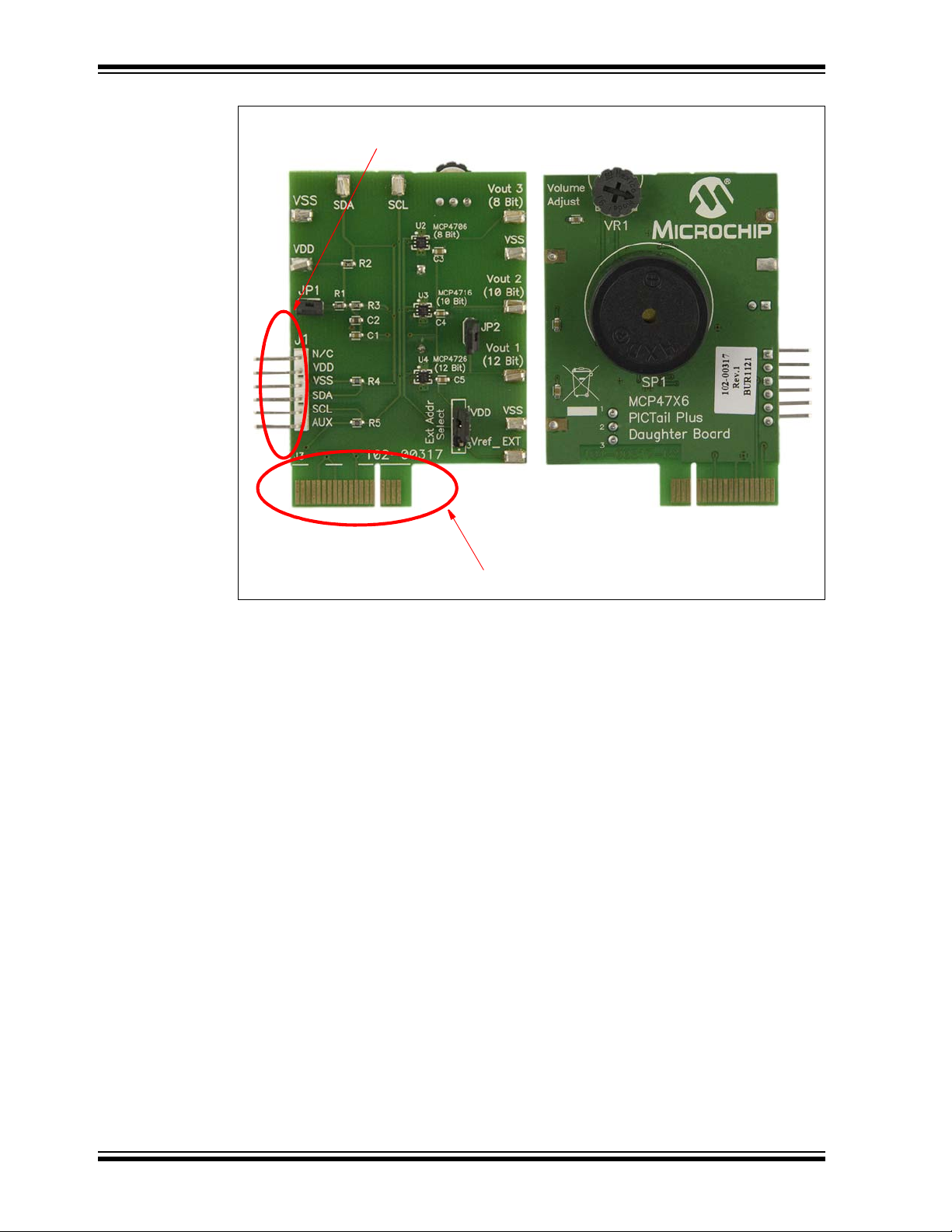
TABLE 1-1: TERMINAL FUNCTION TABLE
Connector/Pin/Terminal Name Functions
J1 Connector Connector for PICkitTM Serial Analyzer.
Note: Do not use this pin when this b oard is us ed wi th the
Explorer 16 Development Board .
J3 Connector Connector for Explorer 16 Development Board.
Note: Do not use this pin when this b oard is us ed wi th the
TM
PICkit
Serial Analyzer.
External Reference Selection
Jumper Pins
JP1 VDD connection through (a) J1 Connector for PICkitTM
JP2 Connecting
V
DD
V
SS
V
1 DAC output terminal f rom MCP4726 (12-bit DAC).
OUT
V
2 DAC output terminal f rom MCP4716 (10-bit DAC).
OUT
V
SDA Connected to I
SCL Connected to I2CTM SCL line
3 DAC output terminal from MCP4706 (8-bit DAC).
OUT
V
REF_EXT
(a) Connect pin 2 to “V
applied at the V
(b) Connect pin 2 to “
externally.
Note: This pin does not affect if VDD is selected a s
reference internally by the configuration bit setting.
Serial Analyzer, or (b) J3 Connector for Explorer 16
Development Board.
V
Note: Do n ot connect thi s jumper if yo u don’t need au dible
sounds.
(a) VDD monitoring terminal w hen JP 1 is co nnecte d (VDD
is provided by the external tools).
(b) VDD connection terminal when JP2 is disconnected.
You can connec t your own
Ground Reference
External Reference connection terminal
OUT
2CTM
REF_EXT
REF_EXT
V
DD
1 (MCP4726 output) to Buzzer.
SDA line
” if external reference is
pin.
” if VDD is used as reference
V
to this pin.
DD
VR1 Volume control for Buzzer 1.
Note: Disconnect JP2 if you don’t need audible sounds.
1.3 I2C ADDRESS BYTE FOR EACH DEVICE
Each DAC device on the board has its own I2C address bits which are preprogrammed
at the factory. Table 1-2 shows the I
TABLE 1-2: I2C ADDRESS BYTE OF EACH DAC DEVICE
Device
MCP4726
(12-bit DAC)
MCP4716
(10-bit DAC)
MCP4726
(8-bit DAC)
where R/W
© 2011 Microchip Technology Inc. DS51932B-page 11
= 0 for write command and 1 for read command.
Address Byte (1st Byte):
Device Code + Address Bits (A2, A1, A0) + R/W
1100-000R/W
1100-001R/W 1100-0010 1100-0011
1100-010R/W
2
C address byte of each device.
I2C Address
Byte for Write
Command
(1st Byte)
1100-0000
1100-0100 1100-0101
I2C Address
Byte for Read
Command
(1st Byte)
1100-0001
Page 12

MCP47X6 PICtail™ Plus Daughter Board User’s Guide
1.4 GETTING STARTED WITH THE EXPLORER 16 DEVELOPMENT BOARD
This section describes how to use the MCP47X6 PICtail™ Plus Daughter Board with
the Explorer 16 Development Board.
After receiving the MCP47X6 PICtail™ Plus Daughter Board, program the 16-bit
PIC24FJ128 MCU on the Explorer 16 Starter Kit using the firmware provided. The user
can download the latest firmware from the Microchip website: www.microchip.com.
• Step 1: Insert the MCP47X6 PICtail™ Plus Daughter Board to the Explorer 16
Development Board. Figure 1-2 shows the configuration when the board is
connected to the Explorer 16 Development Board.
• Step 2: Program the Explorer 16 Development Board using the firmware provided
with this board. Figure 1-3 shows the connection of the MPLAB ICD2 with the
Explorer 16 Development Board for programming.
• Step 3: Once the programming is done, disconnect the MPLAB ICD2 from the
Explorer 16 Development Board.
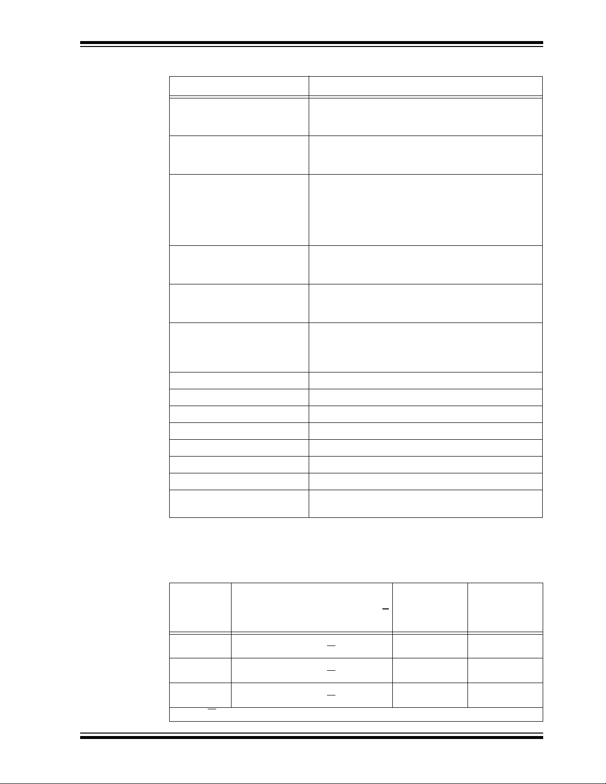
• Step 4: Now you can evaluate the performance of the DAC devices. The LCD on
the Explorer 16 Development Board will display instructions on how to select the
DAC device using the push button switches on the Development Board: (a) S3 for
MCP4726, (b) S6 for MCP4716, and (c) S5 for MCP4706. S4 is used to increment
the DAC code. If you hold down the S4 switch, the DAC code will increase
continuously until it reaches the maximum value, and then it starts from code 0
again. You can observe this event by simply connecting a voltmeter at the V
pin while holding down the S4 switch.
All procedures are very intuitive and interactive using the Push button switches and by
following the instructions on the LCD. The user can observe the DAC output (V
changes using an oscilloscope or voltmeter by pressing the S4 switch. The firmware
provided is an example that can be used as reference for the user’s applications.
OUT
OUT
)
DS51932B-page 12 © 2011 Microchip Technology Inc.
Page 13
Quick Start Instructions
1.5 CONNECTING TO THE EXPLORER 16 STARTER KIT
1. Connect the MCP47X6 PICtail™ Plus Daughter Board to the J5 socket on the
Explorer 16 Development Board as shown in Figure 1-2.
MCP47x6
PICtail Plus
Daughter
Board
S3: Select MCP4726
S6: Select MCP4716
S5: Select MCP4706
S4: Increment DAC Code
Explorer 16 Development Board (P/N DV164033)
FIGURE 1-2: Connecting the MCP47X6 PICtail™ Plus Daughter Board to the
Explorer 16 Development Board.
1.5.1 Programming the PIC24FJ128 MCU
The Explorer 16 Development Board contains the PIC24FJ128 MCU. The user can
download the firmware to the MCU using the MPLAB ICD2 (or ICD3) programmer.
1.5.1.1 THE PIC24FJ128 MCU FIRMWARE FOR THE MCP47X6 PICtail™ PLUS
DAUGHTER BOARD
The original firmware for the Explorer 16 Development Board is modified for the
MCP47X6 PICtail™ Plus Daughter Board demonstration. The firmware uses most of
the original code for the Explorer 16 Development Board except the I
control routines for the PIC24FJ128 MCU.
The following four routines are added or modified from the original Explorer 16
Development Board firmware:
• PIC24ExplDemo_MCP4726_Main.c
• MCP47x6_I2C_Func.c
• Banner_MCP4726_MCP4716_MCP4706.c
• I2C_MCP4726.h
The source codes are compiled by using Microchip’s C30 Compiler and the hex code
is programmed to the MCU using the MPLAB ICD 2. Figure 1-3 shows the connection
between the MPLAB ICD 2 and the Explorer 16 Development Board. Figure 1-4 shows
the MPLAB IDE programming environment.
2
C peripheral
© 2011 Microchip Technology Inc. DS51932B-page 13
Page 14

MCP47X6 PICtail™ Plus Daughter Board User’s Guide
1.5.1.2 FIRMWARE FLOW CHART FOR THE MCP47X6 PICtail™ PLUS
DAUGHTER BOARD
Figure 1-5 shows the flow chart of the firmware. Once the MCU firmware is
programmed, the LCD will display instructions (with repeats) for the next steps. The
firmware us es fo u r push b ut t on sw i t ch es on th e Exp lorer 16 Development Boar d. Th e
features of the switches are:
• S3: Selecting MCP4726 (12-bit DAC). MCP4726 Output is available at V
• S6: Selecting MCP4716 (10-bit DAC). MCP4716 Output is available at V
• S5: Selecting MCP4706 (8-bit DAC). MCP4706 Output is available at V
• S4: Incrementing the DAC code using a write command (writing both DAC register
and EEPROM). The DAC output can be monitored at the V
Figure 1-6 for the V
waveform.
OUT
terminal. See
OUT
The Buzzer is connected to the MCP4726 output through JP2. Please disconnect JP2
if you don’t need audible sounds.
The firmware is interactive with push button switches. Table 1-3 shows the details of
the switches that are used.
The user can switch to other devices by using the device selection push button
switches (S3, S6 and S5) any time. The DAC output can be updated with the S4. The
DAC’s configuration bit settings that are used in the firmware are:
• Gain = 1x, Reference = Internal V
DD
OUT
OUT
OUT
1
2
3
TABLE 1-3: SWITCHES FOR THE FIRMWARE CONTROL
Switch to
Device
MCP4726
(12 bit DAC)
MCP4716
(10 bit DAC)
MCP4726
(8 bit DAC)
Device Selection
Switch
S3
S6 V
S5 V
1.5.1.3 DAC OUTPUT (V
OUT
increment the
DAC Input
Code
)
S4
Output
Terminal
V
1
OUT
2
OUT
3
OUT
Configuration Bit
Settings
Gain = 1x,
= V
V
REF
DD
The MCP47X6 PICtail™ Plus Daughter Board has three DAC output terminals for each
DAC device.
•V
•V
•V
The user can observe the DAC outputs at the V
voltmeter or an oscilloscope. Figure 1-7 shows the I
1: Output from the MCP4726 (12-bit DAC)
OUT
2: Output from the MCP4716 (10-bit DAC)
OUT
3: Output from the MCP4706 (8-bit DAC)
OUT
test terminals using a digital
OUT
2
C clock (SCL) and data (SDA)
signals, and DAC output waveform.
Note: The DAC code is also programmed in EEPROM. The DAC devices on the
MCP47x6 Daughter Board will hold the latest settings when the power
supply is removed. When power supply is back on again (Example:
Remove the board from the Explorer 16 Development Board and connect
again), the same DAC output voltage with the previous settings will be
immediately available at the DAC output terminal.
DS51932B-page 14 © 2011 Microchip Technology Inc.
Page 15

Quick Start Instructions
1.5.1.4 AUDIBLE BUZZER
The MCP47X6 PICtail™ Plus Daughter Board includes a buzzer. This buzzer is directly
connected to the V
by disconnecting JP2. The buzzer volume also can be adjusted by VR1.
of the MCP4726 (12-bit DAC). The user can disable the buzzer
OUT
Explorer 16 Development Board
(P/N DV164033)
FIGURE 1-3: MPLAB ICD2 Connection to Explorer 16 Development Board with the MCP47X6
PICtail™ Plus Daughter Board for Programming.
© 2011 Microchip Technology Inc. DS51932B-page 15
MCP47x6 PICtail Plus
Daughter Board
(P/N ADM00317)
Page 16

MCP47X6 PICtail™ Plus Daughter Board User’s Guide
FIGURE 1-4: MPLAB IDE Programming Environment.
DS51932B-page 16 © 2011 Microchip Technology Inc.
Page 17

Quick Start Instructions
POWER-UP
LCD Display Instructions
NO
Is Any Device Selected?
(S3: MCP4726, S6: MCP4716, S5: MCP4706)
(D9: MCP4726, D7: MCP4716, D3: MCP4706)
START
Turn on LED D3
YES
Turn on LED
Is S4 Pressed?
YES
NO
Send I2C Write Command for DAC Register and EEPROM
DAC Code = DAC Code + 1 LSB
Configuration Register Settings: V
NO
DAC Code = FSR?
YES
Reset DAC Code to 0x00h
Is Any Device Selected?
(S3: MCP4726, S6: MCP4716, S5: MCP4706)
YES
Turn on LED
(D9: MCP4726, D7: MCP4716, D3: MCP4706)
= Internal VDD, Gain = 1x
REF
FIGURE 1-5: Flow Chart for the MCP47X6 PICtail™ Plus Daughter Board Firmware.
© 2011 Microchip Technology Inc. DS51932B-page 17
Page 18

MCP47X6 PICtail™ Plus Daughter Board User’s Guide
2
C
I
Clock Signal
(SCL)
2
I
C
Data Signal
(SDA)
(a) Write command to write DAC Input Register and EEPROM
2
C
I
Clock Signal
(SCL)
2
I
C
Data Signal
(SDA)
DAC Code = 0111 -1110-0011 = 7E3(h) = 2019 (decimal)
Expected DAC Output
V
------------------------- -
REF
4096
Dn
•
5 2019
•
-------------------- 2.465V===
4096
(b) Fast Write Command
DAC Code = 0110-1101-1001 = 6F9 (hex) = 1753 (decimal)
Dn
•
V
Expected DAC Output
FIGURE 1-6: I2C Write Command Waveforms for the MCP4726, with V
DS51932B-page 18 © 2011 Microchip Technology Inc.
DD
----------------------- 4096
•
5 1753
-------------------- 2.1398V===
4096
= VDD and Gain = 1x.
REF
Page 19

I2C
Clock Signal
(SCL)
2
I
C
Data Signal
(SDA)
Quick Start Instructions
A
A
V
OUT
at V
OUT
Pin
: Zoomed-in section for SCL and SDA signals.
A
Write Data (Dn) = 1111 - 01101111 (binary)
V
V
OUT
FIGURE 1-7: I2C SCL, SDA, and V
Code by 1 LSB. The Fast Write Command is Used for this Example.
© 2011 Microchip Technology Inc. DS51932B-page 19
------------------------ 4.823V==
Dn
•
DD
4096
Waveforms for the MCP4726 While Incrementing the DAC
OUT
for V
DD
= 5V
Page 20

MCP47X6 PICtail™ Plus Daughter Board User’s Guide
1.6 GETTING STARTED WITH PICKIT™ SERIAL ANALYZER
The user can connect the MCP47X6 PICtail™ Plus Daughter Board to the PICkit™
Serial Analyzer by setting them up as shown in Figure 1-8.
The following describes how to use them together:
1. Connect the MCP47X6 PICtail™ Plus Daughter Board’s J2 pin socket to the
PICkit™ Serial Analyzer.
2. Connect a digital voltmeter to V
-V
-V
-V
1 for MCP4726
OUT
2 for MCP4716
OUT
3 for MCP4706
OUT
test terminals and VSS:
OUT
MCP47x6 PICtail Plus Daughter Board
DAC analog
Output (V
PICkit Serial Analyzer
USB Cable: Connected between the PICkit Serial Analyzer and Personal Computer.
FIGURE 1-8: MCP47X6 PICtail™ Plus Daughter Board with the PICkit™ Serial Analyzer.
OUT
)
DS51932B-page 20 © 2011 Microchip Technology Inc.
Page 21

Quick Start Instructions
1.6.1 PICkit™ Serial Analyzer PC Soft ware Set-Up for the MCP47x6
Daughter Board
The following steps describe how to set up and use the PICkit™ Serial Analyzer PC
Graphic User Interface (GUI) to evaluate the MCP47X6 PICtail™ Plus Daughter Board.
1. Install the PICkit™ Serial Analyzer software onto your personal computer (PC).
2. Connect the USB cable between the PICkit™ Serial Analyzer and your PC.
3. Run the PICkit™ Serial PC Software. It will open up the graphic user interface
(GUI) as shown. Click the Next button and follow the instruct ions .
4. Select the Communication Mode type: I
2
C Master, and click the Next button.
© 2011 Microchip Technology Inc. DS51932B-page 21
Page 22
MCP47X6 PICtail™ Plus Daughter Board User’s Guide
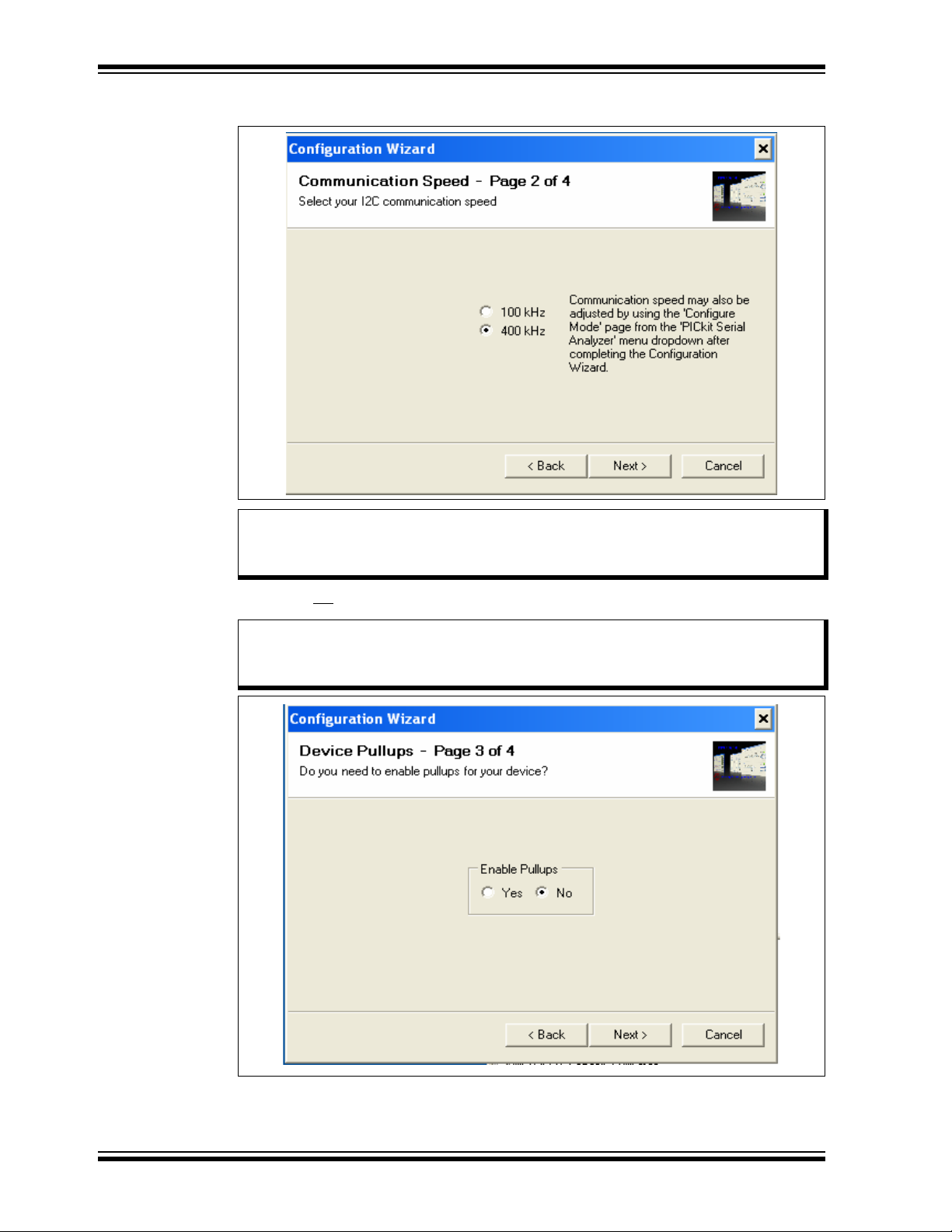
5. Select either 100 kHz or 400 kHz, and click the Next button.
Note: The MCP47x6 devices support the I2C bus data rate up to 3.4 MHz, but the
current version of the PICkit™ Serial Analyzer supports the I
rate up to 400 kHz only.
6. Select No
Note: The MCP47X6 PICtail™ Plus Daughter Board has its own pull-up resistors,
on Enable Pull-ups, and click the Next button.
therefore, you don’t need additional pull-up resistors from the PICkit™
Serial Analyzer.
2
C bus data
DS51932B-page 22 © 2011 Microchip Technology Inc.
Page 23

Quick Start Instructions
7. Select the VDD voltage of the MCP47X6 PICtail™ Plus Daughter Board and click
the
Next button.
Case 1: When you use VDD from the PICkit™ Serial Analyzer
If you choose PICkit™ Serial will power my device and 5 Volts as shown
below, the MCP47X6 PICtail™ Plus Daughter Board is powered by the 5V DC
(range between 4.85V ~ 5V) from the PICkit™ Serial Analyzer through the JP1
jumper. In this case, make sure that the JP1 jumper on the MCP47X6 PICtail™
Plus Daughter Board is connected.
Case 2: When you use your own V
Y ou can also provide your own VDD voltage by applying a VDD voltage at the VDD
terminal. In this case, make sure that the JP1 jumper is disconnected.
DD
© 2011 Microchip Technology Inc. DS51932B-page 23
Page 24

MCP47X6 PICtail™ Plus Daughter Board User’s Guide
8. Click the OK button. You have made all of the PICkit™ Serial Analyzer
Configuration set-ups. You are now ready to program the MCP47X6 PICtail™
Plus Daughter Board using the PICkit™ Serial Analyzer.
DS51932B-page 24 © 2011 Microchip Technology Inc.
Page 25

Quick Start Instructions
1.6.2 Creating Script Files
In order to create a communication between the PICkit™ Serial Analyzer and the
MCP47X6 PICtail™ Plus Daughter Board, a script file is needed. The following
procedure shows how to create script files and how to use them.
Select Communication -----> Script ---> Script Builder.
Note: The MCP47X6 scripts are in a text file on the MCP47X6 PICtailTM Plus
Daughter Board’s product web page. The scripts can be copied into the
TM
PICkit
serial’s CommScripts.txt file.
© 2011 Microchip Technology Inc. DS51932B-page 25
Page 26

MCP47X6 PICtail™ Plus Daughter Board User’s Guide
1.6.2.1 CREATING SCRIPT FILES TO PROGRAM DAC REGISTER AND
EEPROM
1. Click on WriteBlockAddrA8 in “Example I2C Scripts” column.
This will fill in the spaces under Script Detail column.
Modifying the Script Details Parameters:
2. Under the Script Detail column, select the item in the parameter box.
3. Right click the mouse button and an option box appears to the right of your
selection. This gives you the options that are available for the parameter
selected. Select the desired option.
4. Keep the parameters in the same order as shown below.
The following example shows how to create a script file for a Write command (DAC
register and EEPROM) for the MCP4726.
1. Choose these boxes and
right click the mouse button for options available.
2. You can also change the
values or delete the boxes.
3. Make sure the listed
parameters in th e “Script
Detail” should be in the
exact order as shown here.
4. Change the parameter value.
Script Detail
I2CSTART
I2CWRTBYT
04
C0
60
FF
F0
I2CSTOP
Note: All the 8 parameters above must be listed in order. The parameters with * are not
modifiable. Address bits for the MCP4726 is (A2,A1,A0) = (0,0,0). You can
choose any data bit you want in the 3rd and 4th bytes. If you use the above write
data, the MCP4726 device will output:
*
*
-----> This means there are four bytes to send
-----> 1st Write Byte: Address byte = 1100-0000
-----> 2nd Write Byte:1100-0000 (Command + Config.)
-----> 3rd Write Byte: 1111-1111 (Data Byte)
-----> 3rd Write Byte: 1111-0000 (Data Nibble +Don’t care Nibble)
*
V
FFF(hex)(V)
⋅
V
OUT
DD
-------------------------------------------------VDDV()==
4096
DS51932B-page 26 © 2011 Microchip Technology Inc.
Page 27

1st Write Byte
2nd Write Byte
3rd Write Byte
4th Write Byte
Quick Start Instructions
1.6.2.2 SAVING THE SCRIPT FILE AND PROGRAMMING DAC REGISTER
(WRITING BOTH DAC REGISTER AND EEPROM)
1. Change the 3rd and 4th data bytes, if desired, in the Script Detail column.
2. Type in any script name (i.e., MCP4726_WriteEE) in the space below the Script
Name menu.
3. Click Save Script button.
4. Click Execute Script button.
Note: At this point, the PICkit™ Serial transmits a write command of “Write DAC
Register and EEPROM” to the MCP4726 device (address = 000). The
saved file name will appear in Users I2C Scripts column and can be
reused at any time by selecting the file name.
5. The analog output voltage of the MCP4726 will be monitored at V
on the Daughter Board.
Note: When you click on the “Execute Script” menu, the “Busy” LED on the PICkit
Serial Analyzer will momentarily turn on and then turn off. If the LED
remains ON, a communications problem has occurred. Remove the PICkit
Serial Analyzer from the personal computer and recheck the parameter
value in the order of the parameters under the Script Detail column. Try
again until the “Busy” LED goes OFF after executing the write command.
1 terminal
OUT
© 2011 Microchip Technology Inc. DS51932B-page 27
Page 28
MCP47X6 PICtail™ Plus Daughter Board User’s Guide
1.6.2.3 CREATING A SCRIPT FILE TO PROGRAM THE DAC REGISTER WITH
FAST MODE COMMAND
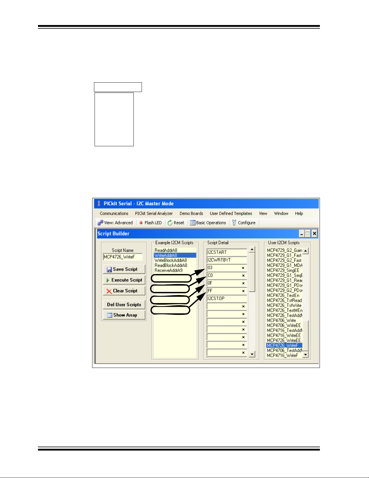
1. Get a new script file by selecting the WriteAddrA8 from the “Example I2C
Scripts” column.
2. Modify the Script Detail column as shown bel ow:
Script Detail
I2CWRTBYT
I2CSTART
03
C0
0F
FF
I2CSTOP
3. Type in the script name (i.e., MCP4726_WriteF) in the space below the Script
Name menu.
4. Click the Execute Script button.
*
*
-------> This means Master will send three bytes
-------> 1st Write Byte: Address byte = 1100-0000
-------> 2nd Write Byte: 0000-FFFF (Data Byte)
-------> 3rd Write Byte: FFFF-FFFF (Data Nibble + Don’t care Nibble)
*
VDDDn
Now the device will output V
OUT
⋅
----------------------4096
⋅
5V 800 hex()
---------------------------------- 2 . 5 V== =
4096
3 Bytes to Send
1st Write Byte
2nd Write Byte
3rd Write Byte
DS51932B-page 28 © 2011 Microchip Technology Inc.
Page 29

Quick Start Instructions
1.6.3 Verifying the EEPROM Data
One of the important features of the MCP4706 devices is the nonvolatile memory.
When the device is first powered up, it outputs an analog voltage corresponding to the
data in the EEPROM. The user can confirm this feature using the following procedures:
1. Program the EEPROM memory. Refer to Section 1.6.2.1 “Creating Script
Files to Program DAC Register and EEPROM”.
2. Remove power (V
remove the daughter board from the PICkit™ Serial Analyzer.
3. Reconnect power (V
to the PICkit™ Serial Analyzer.
4. You can confirm that the programmed DAC output at the DAC output terminal
(V
1, V
OUT
OUT
1.6.4 Reading both the DAC Register and EEPROM data:
You can read back the DAC code stored in the DAC register and EEPROM with the
following steps:
1. Create a read command script file name as shown below and execute it.
2. The results (DAC code and EEPROM data) will appear on the PICkit™ Serial
Transactions page.
) from the MCP47X6 PICtail™ Plus Daughter Board, or
DD
) to the Daughter Board or reconnect the Daughter Board
DD
2, V
3) by using a digital voltmeter.
OUT
© 2011 Microchip Technology Inc. DS51932B-page 29
Page 30

MCP47X6 PICtail™ Plus Daughter Board User’s Guide
Requesting
6 Bytes
Written Data
using a Write Command
Reading Data
using a Read Command
EEPROM Data (Configuration bits + DAC Code)
DAC Register Data (Configuration bits + DAC Code)
1.7 EXAMPLES FOR OTHER DEVICES (MCP4706, MCP4716)
The examples shown in the previous sections use the I2C address bits of the MCP4726
(A2, A1, A0 = 0,0,0). The same procedure is also applicable for the remaining
two devices (MCP4706, MCP4716) by simply using the right address byte for each
device. Table 1-2 shows the address byte of each device. Refer to the
MCP4706/MCP4716/MCP4726 Data Sheet for the data format of each command.
DS51932B-page 30 © 2011 Microchip Technology Inc.
Page 31

Quick Start Instructions
1.8 PROGRAMMING EXAMPLE USING THE PICKIT™ SERIAL ANALYZER
The following example shows how to set DAC code for the desired DAC output voltage
using the Fast Write command.
See the MCP4706/MCP4716/MCP4726 Data sheet for more details on the data
formats for each device.
1 1 0 0 A2 A1 A0 R/W
(A2, A1, A0) = (0,0,0) for MCP4726
Device Code
Address Bits
FIGURE 1-9: MCP47x6 Device Address Byte.
Targeted DAC Output = INL x Dn = 2.5V
INL = V
(a) MCP4726
Start 00xC0 0 PD1 PD0 D11 D10 D9 D8 D7 D5D6 D4 D3 D1D2 D0 STOP ACK ACK
Address Byte:
when (A2 A1 A0) = 000
REF
ACK
/2N = 5V/2N
= 5V/4096 = 1.2207 mV for 12-bit DAC (MCP4726)
= 5V/1024 = 4.8828 mV for 10-bit DAC (MCP4716)
= 5V/256 = 19.53125mV for 8-bit DAC (MCP4706)
2.5V
D
-----------
== ==
n
INL
(1 0 0 0 0 0 0 0 0 0 0 0)
2.5V
------------------------- 2048 2
1.2207mV
0x08h
* Factory Programmed Address Bits:
= (0,0,1) for MCP4716
= (0,1,0) for MCP4706
11
0x00h
11
2
=
(b) MCP4716
2.5V
== ==
-----------
D
n
INL
Start 00xC2 0 PD1 PD0 D9 D8 D7 D6 D5 D4 D2D3 D1 D0
ACK
(1 0 0 0 0 0 0 0 0 0 0 0)
2.5V
-------------------------5122
4.8828mV
0x08h
Address Byte:
=
9
2
when (A2 A1A0) = 001
(c) MCP4706
2.5V
== ==
D
-----------
n
INL
Start 00xC4 0 PD1 PD0 X X X X D7 D6 D4D5 D3 D2
ACK
( 0 0 0 0)
2.5V
-------------------------------1282
19.53125mV
(1 0 0 0 0 0 0 0 )
0x00h
Address Byte:
when (A2 A1A0) = 010
FIGURE 1-10: Fast Mode Write Command for Targeted V
OUT
9
0x00h
7
0x80h = 2
= 2.5V when V
7
X
D1
REF
X
D0
= 5V.
STOPACK ACK
STOPACK ACK
© 2011 Microchip Technology Inc. DS51932B-page 31
Page 32

MCP47X6 PICtail™ Plus Daughter Board User’s Guide
NOTES:
DS51932B-page 32 © 2011 Microchip Technology Inc.
Page 33

Appendix A. Schematic and Layouts
A.1 INTRODUCTION
This appendix contains the following schematics and layouts for the MCP47x6
PICtail™ Plus Daughter Board:
• Board – Schematic
• Board – Top Silk and Pads
• Board – Top Copper, Top Pads and Top Silk
• Board – Bottom Silk and Pads
• Board – Bottom Copper, Bottom Pads and Silk
MCP47X6 PICtail™ PLUS DAUGHTER
BOARD USER’S GUIDE
© 2011 Microchip Technology Inc. DS51932B-page 33
Page 34

MCP47X6 PICtail™ Plus Daughter Board User’s Guide
A.2 BOARD – SCHEMATIC
M
DS51932B-page 34 © 2011 Microchip Technology Inc.
Page 35

A.3 BOARD – TOP SILK AND PADS
Schematic and Layouts
© 2011 Microchip Technology Inc. DS51932B-page 35
Page 36

MCP47X6 PICtail™ Plus Daughter Board User’s Guide
A.4 BOARD – TOP COPPER, TOP PADS AND TOP SILK
DS51932B-page 36 © 2011 Microchip Technology Inc.
Page 37

A.5 BOARD – BOTTOM SILK AND PADS
Schematic and Layouts
© 2011 Microchip Technology Inc. DS51932B-page 37
Page 38

MCP47X6 PICtail™ Plus Daughter Board User’s Guide
A.6 BOARD – BOTTOM COPPER, BOTTOM PADS AND SILK
DS51932B-page 38 © 2011 Microchip Technology Inc.
Page 39

MCP47X6 PICtail™ PLUS DAUGHTER
BOARD USER’S GUIDE
Appendix B. Bill Of Materials (BOM)
TABLE B-1: BILL OF MATERIALS (BOM)
Qty Reference Description Manufacturer Part Number
7 C1, C3, C4,
C5, C6, C7, C8
1 C2 CAP 1.0UF 16V CERAMIC X5R 0603 Panasonic - ECG ECJ-1VB1C105K
1 J1 CONN HEADER 6 POS. 100 R/A TIN Molex/Waldom Electronics
1 JMP1 CONN HEADER 3 POS. 100" STR
3JMP1, JP1,
JP2
2 JP1, JP2 CONN HEADER 2 POS. 100 VERT
1 PCB RoHS Compliant Bare PCB,
1 R1 RES 100 OHM 1/10W 1% 0603 SMD Panasonic - ECG ERJ-3EKF1000V
2 R2, R3 RES 10.0K OHM 1/10W 1% 0603
2 R4, R5 RES 10 OHM 1/10W 5% 0603 SMD Panasonic - ECG ERJ-3GEYJ100V
1 U2 8-/10-/12-Bit Voltage Output
1 U3 8-/10-/12-Bit Voltage Output
1 U4 8-/10-/12-Bit Voltage Output
10 Vout1,Vout2,
Vout3, VSS,
EXT, VSS,
SDA, SCL,
VSS, AVDD
1 VR1 POT 5.0K OHM THUMBWHEEL
1 SP1 BUZZER PIEZO 3kHz 24mm PIC MT Mallory Sonalert Products, Inc. PK-21N30PQ
Note 1: The components listed in t his Bill of Materi als are repr esent ativ e of the PCB asse mbly. The released BOM
used in manufacturing uses all RoHS-compliant components.
CAP.1UF 16V CERAMIC X7R 0603 Panasonic - ECG ECJ-1VB1C104K
22-05-2061
Corp
Molex/Waldom Electronics
TIN
SHUNT LP W/HANDLE 2 POS. 30AU
*Bag shunts with kit*
TIN
MCP4726, MCP4716 MCP4706
TM
PICtail
SMD
Digital-to-Analog Conv erte r with
EEPROM
Digital-to-Analog Conv erte r with
EEPROM
Digital-to-Analog Conv erte r with
EEPROM
PC TEST POINT COMPACT SMT Keystone Electronics 5016
CERM ST
Plus Daughter Board
Corp
Tyco Electronics/Amp 881545-2
Molex/Waldom Electronics 22-03-2021
- 104-00317
Panasonic - ECG ERJ-3EKF1002V
Microchip Technology Inc. MCP4706A2T-E/MA
Microchip Technology Inc. MCP4716A1T-E/MA
Microchip Technology Inc. MCP4726A0T-E/MA
Bourns Inc. 3352T-1-502
90120-0123
© 2011 Microchip Technology Inc. DS51932B-page 39
Page 40

Worldwide Sales and Service
AMERICAS
Corporate Office
2355 West Chandler Blvd.
Chandler, AZ 85224-6199
Tel: 480-792-7200
Fax: 480-792-7277
Technical Support:
http://www.microchip.com/
support
Web Address:
www.microchip.com
Atlanta
Duluth, GA
Tel: 678-957-9614
Fax: 678-957-1455
Boston
Westborough, MA
Tel: 774-760-0087
Fax: 774-760-0088
Chicago
Itasca, IL
Tel: 630-285-0071
Fax: 630-285-0075
Cleveland
Independence, OH
Tel: 216-447-0464
Fax: 216-447-0643
Dallas
Addison, TX
Tel: 972-818-7423
Fax: 972-818-2924
Detroit
Farmington Hills, MI
Tel: 248-538-2250
Fax: 248-538-2260
Indianapolis
Noblesville, IN
Tel: 317-773-8323
Fax: 317-773-5453
Los Angeles
Mission Viejo, CA
Tel: 949-462-9523
Fax: 949-462-9608
Santa Clara
Santa Clara, CA
Tel: 408-961-6444
Fax: 408-961-6445
Toronto
Mississauga, Ontario,
Canada
Tel: 905-673-0699
Fax: 905-673-6509
ASIA/PACIFIC
Asia Pacific Office
Suites 3707-14, 37th Floor
Tower 6, The Gateway
Harbour City, Kowloon
Hong Kong
Tel: 852-2401-1200
Fax: 852-2401-3431
Australia - Sydney
Tel: 61-2-9868-6733
Fax: 61-2-9868-6755
China - Beijing
Tel: 86-10-8569-7000
Fax: 86-10-8528-2104
China - Chengdu
Tel: 86-28-8665-5511
Fax: 86-28-8665-7889
China - Chongqing
Tel: 86-23-8980-9588
Fax: 86-23-8980-9500
China - Hangzhou
Tel: 86-571-2819-3187
Fax: 86-571-2819-3189
China - Hong Kong SAR
Tel: 852-2401-1200
Fax: 852-2401-3431
China - Nanjing
Tel: 86-25-8473-2460
Fax: 86-25-8473-2470
China - Qingdao
Tel: 86-532-8502-7355
Fax: 86-532-8502-7205
China - Shanghai
Tel: 86-21-5407-5533
Fax: 86-21-5407-5066
China - Shenyang
Tel: 86-24-2334-2829
Fax: 86-24-2334-2393
China - Shenzhen
Tel: 86-755-8203-2660
Fax: 86-755-8203-1760
China - Wuhan
Tel: 86-27-5980-5300
Fax: 86-27-5980-5118
China - Xian
Tel: 86-29-8833-7252
Fax: 86-29-8833-7256
China - Xiamen
Tel: 86-592-2388138
Fax: 86-592-2388130
China - Zhuhai
Tel: 86-756-3210040
Fax: 86-756-3210049
ASIA/PACIFIC
India - Bangalore
Tel: 91-80-3090-4444
Fax: 91-80-3090-4123
India - New Delhi
Tel: 91-11-4160-8631
Fax: 91-11-4160-8632
India - Pune
Tel: 91-20-2566-1512
Fax: 91-20-2566-1513
Japan - Yokohama
Tel: 81-45-471- 6166
Fax: 81-45-471-6122
Korea - Daegu
Tel: 82-53-744-4301
Fax: 82-53-744-4302
Korea - Seoul
Tel: 82-2-554-7200
Fax: 82-2-558-5932 or
82-2-558-5934
Malaysia - Kuala Lumpur
Tel: 60-3-6201-9857
Fax: 60-3-6201-9859
Malaysia - Penang
Tel: 60-4-227-8870
Fax: 60-4-227-4068
Philippines - Manila
Tel: 63-2-634-9065
Fax: 63-2-634-9069
Singapore
Tel: 65-6334-8870
Fax: 65-6334-8850
Tai wan - Hsin Chu
Tel: 886-3-5778-366
Fax: 886-3-5770-955
Taiwan - Kaohsiung
Tel: 886-7-536-4818
Fax: 886-7-330-9305
Taiwan - Taipei
Tel: 886-2-2500-6610
Fax: 886-2-2508-0102
Thailand - Bangkok
Tel: 66-2-694-1351
Fax: 66-2-694-1350
EUROPE
Austria - Wels
Tel: 43-7242-2244-39
Fax: 43-7242-2244-393
Denmark - Copenhagen
Tel: 45-4450-2828
Fax: 45-4485-2829
France - Paris
Tel: 33-1-69-53-63-20
Fax: 33-1-69-30-90-79
Germany - Munich
Tel: 49-89-627-144-0
Fax: 49-89-627-144-44
Italy - Milan
Tel: 39-0331-742611
Fax: 39-0331-466781
Netherlands - Drunen
Tel: 31-416-690399
Fax: 31-416-690340
Spain - Madrid
Tel: 34-91-708-08-90
Fax: 34-91-708-08-91
UK - Wokingham
Tel: 44-118-921-5869
Fax: 44-118-921-5820
08/02/11
DS51932B-page 40 © 2011 Microchip Technology Inc.
 Loading...