

Page 1
MCP4728
Evaluation Board
User’s Guide
© 2009 Microchip Technology Inc. DS51837A
Page 2
Note the following details of the code protection feature on Microchip devices:
• Microchip products meet the specification contained in their particular Microchip Data Sheet.
• Microchip believes that its family of products is one of the most secure families of its kind on the market today, when used in the
intended manner and under normal conditions.
• There are dishonest and possibly illegal methods used to breach the code protection feature. All of these methods, to our
knowledge, require using the Microchip products in a manner outside the operating specifications contained in Microchip’s Data
Sheets. Most likely, the person doing so is engaged in theft of intellectual property.
• Microchip is willing to work with the customer who is concerned about the integrity of their code.
• Neither Microchip nor any other semiconductor manufacturer can guarantee the security of their code. Code protection does not
mean that we are guaranteeing the product as “unbreakable.”
Code protection is constantly evolving. We at Microchip are committed to continuously improving the code protection features of our
products. Attempts to break Microchip’s code protection feature may be a violation of the Digital Millennium Copyright Act. If such acts
allow unauthorized access to your software or other copyrighted work, you may have a right to sue for relief under that Act.
Information contained in this publication regarding device
applications and the like is provided only for your convenience
and may be superseded by updates. It is your responsibility to
ensure that your application meets with your specifications.
MICROCHIP MAKES NO REPRESENTATIONS OR
WARRANTIES OF ANY KIND WHETHER EXPRESS OR
IMPLIED, WRITTEN OR ORAL, STATUTORY OR
OTHERWISE, RELATED TO THE INFORMATION,
INCLUDING BUT NOT LIMITED TO ITS CONDITION,
QUALITY, PERFORMANCE, MERCHANTABILITY OR
FITNESS FOR PURPOSE. Microchip disclaims all liability
arising from this information and its use. Use of Microchip
devices in life support and/or safety applications is entirely at
the buyer’s risk, and the buyer agrees to defend, indemnify and
hold harmless Microchip from any and all damages, claims,
suits, or expenses resulting from such use. No licenses are
conveyed, implicitly or otherwise, under any Microchip
intellectual property rights.
Trademarks
The Microchip name and logo, the Microchip logo, dsPIC,
K
EELOQ, KEELOQ logo, MPLAB, PIC, PICmicro, PICSTART,
rfPIC and UNI/O are registered trademarks of Microchip
Technology Incorporated in the U.S.A. and other countries.
FilterLab, Hampshire, HI-TECH C, Linear Active Thermistor,
MXDEV, MXLAB, SEEVAL and The Embedded Control
Solutions Company are registered trademarks of Microchip
Technology Incorporated in the U.S.A.
Analog-for-the-Digital Age, Application Maestro, CodeGuard,
dsPICDEM, dsPICDEM.net, dsPICworks, dsSPEAK, ECAN,
ECONOMONITOR, FanSense, HI-TIDE, In-Circuit Serial
Programming, ICSP, ICEPIC, Mindi, MiWi, MPASM, MPLAB
Certified logo, MPLIB, MPLINK, mTouch, nanoWatt XLP,
Omniscient Code Generation, PICC, PICC-18, PICkit,
PICDEM, PICDEM.net, PICtail, PIC
32
logo, REAL ICE, rfLAB,
Select Mode, Total Endurance, TSHARC, WiperLock and
ZENA are trademarks of Microchip Technology Incorporated
in the U.S.A. and other countries.
SQTP is a service mark of Microchip Technology Incorporated
in the U.S.A.
All other trademarks mentioned herein are property of their
respective companies.
© 2009, Microchip Technology Incorporated, Printed in the
U.S.A., All Rights Reserved.
Printed on recycled paper.
Microchip received ISO/TS-16949:2002 certification for its worldwide
headquarters, design and wafer fabrication facilities in Chandler and
T empe, Arizona; Gresham, Oregon and design centers in California
and India. The Company’s quality system processes and procedures
are for its PIC
devices, Serial EEPROMs, microperipherals, nonvolatile memo ry and
analog products. In addition, Microchip’s quality system for the desig n
and manufacture of development systems is ISO 9001:2000 certified.
®
MCUs and dsPIC® DSCs, KEELOQ
®
code hopping
DS51837A-page ii © 2009 Microchip Technology Inc.
Page 3

MCP4728 EVALUATION BOARD
USER ’S GUIDE
Table of Contents
Preface ...........................................................................................................................1
Introduction............................................................................................................1
Document Layout..................................................................................................1
Conventions Used in this Guide............................................................................2
Recommended Reading........................................................................................2
The Microchip Web Site........................................................................................ 3
Customer Support.................................................................................................3
Document Revision History...................................................................................3
Chapter 1. Quick Start Instructions
1.1 Introduction .....................................................................................................5
1.2 Description of the MCP4728 Evaluation Board ..............................................5
1.3 Getting Started with PICkit Serial Analyzer ....................................................7
Appendix A. Schematic and Layouts
A.1 Introduction ..................................................................................................35
A.2 Board – Schematic .......................................................................................36
A.3 Board – Top Silk, Top Pads and Top Copper .............................................. 37
A.4 Board – Top Copper and Pads .................................................................... 38
A.5 Board – Top Pads and Silk .......................................................................... 39
A.6 Board – Bottom Copper Layer ..................................................................... 40
Appendix B. Bill Of Materials (BOM)
Appendix C. MCP4728 Read/Write Commands
C.1 Introduction ..................................................................................................43
Worldwide Sales and Service ....................................................................................46
© 2009 Microchip Technology Inc. DS51837A-page iii
Page 4

MCP4728 Evaluation Board User’s Guide
NOTES:
DS51837A-page iv © 2009 Microchip Technology Inc.
Page 5

MCP4728 EVALUATION BOARD
USER ’S GUIDE
Preface
NOTICE TO CUSTOMERS
All documentation becomes dated, and this manual is no exception. Microchip tools and
documentation are constantly evolving to meet customer needs, so some actual dialogs
and/or tool descriptions may differ from those in this document. Please refer to our web site
(www.microchip.com) to obtain the latest documentation available.
Documents are identified with a “DS” number. This number is located on the bottom of each
page, in front of the page number. The numbering convention for the DS number is
“DSXXXXXA”, where “XXXXX” is the document number and “A” is the revision level of the
document.
For the most up-to-date information on development tools, see the MPLAB
Select the Help menu, and then Topics to open a list of available on-line help files.
®
IDE on-line help.
INTRODUCTION
This chapter contains general information that will be useful to know before using the
MCP4728 Evaluation Board. Items discussed in this chapter include:
• Document Layout
• Conventions Used in this Guide
• Recommended Reading
• The Microchip Web Site
• Customer Support
DOCUMENT LAYOUT
This document describes how to use the MCP47 28 Evalu a tio n Boa rd with PICkitTM
Serial Analyzer. The manual layout is as follows:
• Chapter 1. “Quick Start Instructions” – this chapter provide s an overview of the
MCP4728 Evaluation Board and instructions on how to use the MCP4728
Evaluation Board with the PICkit
• Appendix A. “Schematic and Layouts” – shows the schematic and layout
diagrams for the MCP4728 Evaluation Board.
• Appendix B. “Bill Of Materials (BOM)” – lists the parts used to build the
MCP4728 Evaluation Board.
• Appendix C. “MCP4728 Read/Write Commands” – shows the read/write commands for the MCP4728 Evaluation Board.
TM
Serial Analyzer.
© 2009 Microchip Technology Inc. DS51837A-page 1
Page 6
MCP4728 Evaluation Board User’s Guide
CONVENTIONS USED IN THIS GUIDE
This manual uses the following documentation conventions:
DOCUMENTATION CONVENTIONS
Description Represents Examples
Code (Courier font):
Plain characters Sample code
Filenames and paths
Angle brackets: < > Variables <label>, <exp>
Square brackets [ ] Optional arguments MPASMWIN [main.asm]
Curly brackets and pipe
character: { | }
Lowercase characters in
quotes
Ellipses... Used to imply (but not show) addi-
0xnnn A hexadecimal number where n is a
Italic characters A variable argument; it can be either a
Interface (Arial font):
Underlined, italic text
with right arrow
Bold characters A window or dialog button to click OK, Cancel
Characters in angle
brackets < >
Documents (Arial font):
Italic characters Referenced books MPLAB
Choice of mutually exclusive argu-
ments; An OR selection
Type of data
tional text that is not relevant to the
example
hexadecimal digit
type of data (in lowercase characters)
or a specific example (in uppercase
characters).
A menu selection from the menu bar File > Save
A key on the keyboard <Tab>, <Ctrl-C>
#define START
c:\autoexec.bat
errorlevel {0|1}
“filename”
list
[“list_option...,
“list_option”]
0xFFFF, 0x007A
char isascii (char,
ch);
®
IDE User’s Guide
RECOMMENDED READING
This user's guide describes how to use MCP4728 Evaluation Board. Other useful
documents are listed below. The following Microchip documents are available and
recommended as supplemental reference resources.
PICkit™ Serial Analyzer User’s Guide, DS51647
Consult this document for instructions on how to use the PICkit Serial Analyzer
hardware and software.
MCP4728 Data Sheet, “12-Bit, Quad Digital-to-Analog Converter with EEPROM
Memory” DS22187
This data sheet provides detailed information regarding for the MCP4728
Digital-to-Analog Converter.
DS51837A-page 2 © 2009 Microchip Technology Inc.
Page 7

THE MICROCHIP WEB SITE
Microchip provides online support via our web site at www.microchip.com. This web
site is used as a means to make files and information easily available to customers.
Accessible by using your favorite Internet browser , the web site contains the following
information:
• Product Support – Data sheets and errata, application notes and sample
programs, design resources, user’s guides and hardware support documents,
latest software releases and archived software
• General Technical Support – Frequently Asked Questions (FAQs), technical
support requests, online discussion groups, Microchip consultant program
member listing
• Business of Microchip – Product Selector Guide, latest Microchip press
releases, listing of seminars and events, listings of Microchip sales offices,
distributors and factory representatives
CUSTOMER SUPPORT
Users of Microchip products can receive assistance through several channels:
• Distributor or Representative
• Local Sales Office
• Field Application Engineer (FAE)
• Technical Support
• Development Systems Information Line
Customers should contact their distributor, representative or field application engineer
(FAE) for support. Lo cal sales offices are also available to help customers. A listing of
sales offices and locations is included in the back of this document.
Technical support is available through the web site at: http://support.microchip.com
Preface
DOCUMENT REVISION HISTORY
Revision A (June 2009)
• Initial Release of this Document.
© 2009 Microchip Technology Inc. DS51837A-page 3
Page 8

MCP4728 Evaluation Board User’s Guide
NOTES:
DS51837A-page 4 © 2009 Microchip Technology Inc.
Page 9

MCP4728 EVALUATION BOARD
USER ’S GUIDE
Chapter 1. Quick Start Instructions
1.1 INTRODUCTION
The following sections provide an overview of the MCP4728 Evaluation Board and
instructions on how to program the DAC register and the EEPROM of the MCP4728
using the PICkit
• Description of the MCP4728 Evaluation Board
• How to use the MCP4728 Evaluation Board with the PICkit Serial Analyzer
1.2 DESCRIPTION OF THE MCP4728 EVALUATION BOARD
The purpose of the MCP4728 Evaluation Board is to provide an easy way o f evaluating
the MCP4728’s performance and functionality with a minimum of work.
The MCP4728 Evaluation Board contains a MCP4728 (which is a 4-channel, 12-bit
Digital-to-Analog Converter), an interface conn ector for the PICkit Serial Analyzer, and
2
I
C test point terminals.The user can evaluate this board by using the PICkit Serial
Analyzer or by providing the I
terminals.
Using the MCP4728 Evaluation Board, the user can evaluate the functionality of the
MCP4728 device, such as: (a) Writing and reading the DAC registers and EEPROM of
each channel, (b) Selecting the reference voltage, (c) Measuring the DAC output
voltage, (d) Checking the LDAC
The MCP4728 Evaluation Board is designed to work friendly with the PICkit Serial
Analyzer (DV164122). The PICkit Serial Analyzer (P/N: DV164122) is used for writing
and reading the DAC configuration and register data. The PICkit Serial Analyzer
consists of hardware and PC GUI. It is highly recommended that the users order this
MCP4728 Evaluation Board and the PICkit Serial Analyze r at same tim e.
• The MCP4728 supports sta ndard mode (100kHz), fast mode (400 kHz), and high
speed mode (3.4 MHz) of the I
has 5 kΩ for the I
needs to evaluate the device with high speed mode (3.4 MHz), please replace the
R1 and R2 with lower values (less than 1 kΩ).
TM
Serial Analyzer. The following sections cover the topics:
2
C serial communication signals through the I2C test
pin feature, etc.
2
2
C pull-up resistors and supports up to the fast mode. If the user
C serial communications. This evaluation boar d
Note: The MCP4728 Evaluation Board can be used without the PICkit Serial
Analyzer as long as the V
connector. This board does not include MCU.
The MCP4728 Evaluation Board has test points for SDL, SDA, and DAC outputs. By
connecting an oscilloscope to these I
communications through the I
V
terminals) using a multimeter. Refer to Appe ndix A. “Schematic and Layouts”.
OUT
© 2009 Microchip Technology Inc. DS51837A-page 5
2C™
, SCL, and SDA are provided through the J1
DD
2
C test points, the user can examine the data
bus line and observe the resulting analog output (at
Page 10
MCP4728 Evaluation Board User’s Guide
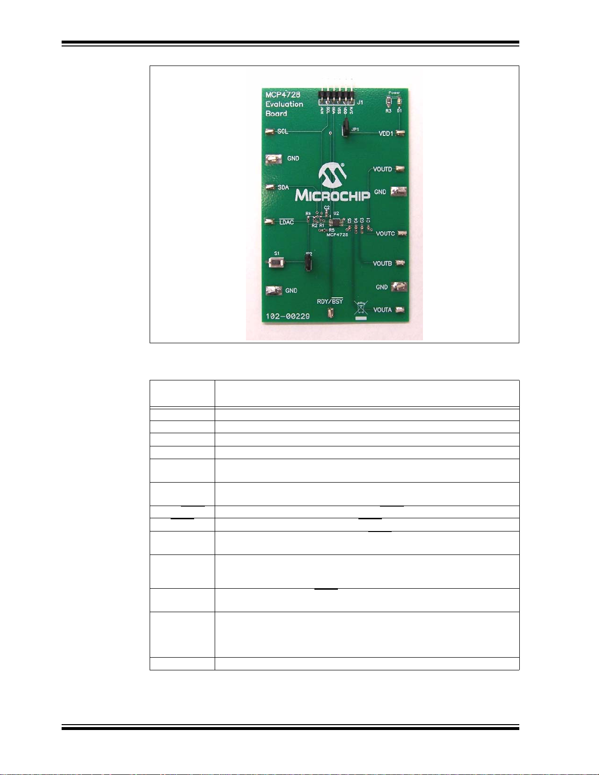
FIGURE 1-1: Front View of the MCP4728 Evaluation Board.
TABLE 1-1: TEST TERMINALS ON THE MCP4728 EVALUATION BOARD
Test
Terminals
A DAC channel A output
V
OUT
B DAC channel B output
V
OUT
V
C DAC channel C output
OUT
D DAC channel D output
V
OUT
SCL This terminal is connected to the I
SDA This terminal is connected to the I
RDY/BUSY
LDAC
This terminal is used to monitor the RDY/BUSY pin of the MCP4728 device.
Access terminal to the LDAC pin of the MCP4728.
S1 Switch to change the logic input to the LDAC
JP1 Jumper to select the V
connected, the V
DD
from the J1 connector is connected. If disconnected, it
DD
selects the V
JP2 Jumper to connect the LDAC pin to VSS. (You can disconnect this jumper
VDD1 V
If the V
is provided from J1 connector (PICkit Serial Analyzer), then this
DD
DD
test point monitors the V
GND Connected to common ground plane of the PC Board.
Note 1: This terminal is used to monitor the SCL or SDA signals. You can also provide the
SCL or SDA signals through these pins.
Description
2
C SCL pin of the MCP4728.
(See Note 1).
2
C SDA pin of the MCP4728.
(See Note 1).
input pin. It provides logic “low”
when pressed.
source to the MCP4728 Evaluation Board. If it is
source from VDD1 terminal.
DD
when S1 is used.)
monitoring or connection pin.
voltage. You can also connect a new VDD to this
DD
test terminal.
DS51837A-page 6 © 2009 Microchip Technology Inc.
Page 11

Quick Start Instructions
1.3 GETTING STARTED WITH PICKIT SERIAL ANALYZER
Figure 1-1 shows the MCP4728 Evaluation Board, and Figure 1-2 shows the
connection of the MCP4728 Evaluation Board and PICkit Serial Analyzer.
The following steps describe how to use them together:
1. Connect the MCP4728 Evaluation Board’s 6-pin socket to the PICkit Serial
Analyzer as shown in Figure 1-2.
2. Connect the oscilloscope probes to the SCL and SDA test terminals (optional).
3. Connect a multimeter to one of the DAC’s output test terminal.
4. V
• I
• A2, A1, A0 Address Bits: Pre-programmed to‘000’.
5. Connecting V
6. Use the PICkit Serial Analyzer PC GUI to send I
Selection: Y ou can use the VDD from the PICkit Serial Analyzer or use your
DD
own external V
(a) Connect JP1, if using V
(b) Disconnect JP1 and apply V
2
C device code of MCP4728: ‘1100’
Analyzer will provide V
. The JP1 connector selects the VDD path.
DD
from PICkit Serial Analyzer,
DD
at VDD1 pin, if you are using an external VDD.
DD
: LED D1 turns on when VDD is applied. The PICkit Serial
DD
automatically, if it is connected to the PC. Make sure
DD
LED D1 turns on.
2
C write and read commands.
© 2009 Microchip Technology Inc. DS51837A-page 7
Page 12

MCP4728 Evaluation Board User’s Guide
MCP4728 Evaluation Board
Personal
Computer
Connected between the
PICkit Serial Analyzer
and Personal Computer
DAC Output
(Channel B)
PICkit Serial Analyzer
USB Cable
.
FIGURE 1-2: MCP4728 Evaluation Board with the PICkit Serial Analyzer.
DS51837A-page 8 © 2009 Microchip Technology Inc.
Page 13
Quick Start Instructions
1.3.1 PICkit Serial Analyzer PC Software Setup for the MCP4728
Evaluation Board
The following steps describe how to set up and use the PICkit Serial Analyzer PC
Graphic User Interface (GUI).
1. Install the PICkit Serial Analyzer software onto your personal computer (PC).
2. Connect the USB cable between the PICkit Serial Analyzer and the PC.
3. Run the PICkit Serial PC Software: It will open to the following GUI. Click the
Next button and follow the instructions.
FIGURE 1-3: PICkit Serial Analyzer Configuration Wizard Welcome Window.
4. Select the Communication Mode type: I
2
C Master, and click the Next button.
FIGURE 1-4: Step 1 - Communication Mode Selection.
© 2009 Microchip Technology Inc. DS51837A-page 9
Page 14

MCP4728 Evaluation Board User’s Guide
5. Select 100 kHz or 400 kHz. Either one will be fine. Click the Next button.
FIGURE 1-5: Step 2 - I2C Communication Speed Selection.
Note: The MCP4728 device supports the I2C bus data rate up to 3.4 MHz, but the
current version of the PICkit Serial Analyzer supports the I
2
C bus data rate
up to 400 kHz only.
6. Select No on Enable Pull-ups and click the Next button.
Note: The MCP4728 Evaluation Board has its own pull-up resistors.
FIGURE 1-6: Step 3 - Device Pull-Ups Window.
DS51837A-page 10 © 2009 Microchip Technology Inc.
Page 15
Quick Start Instructions
7. Select the VDD voltage of the MCP4728 Evaluation Board and click the Next
button.
Case 1: When you use VDD from the PICkit Serial Analyzer:
If you choose PICkit Serial will power your device and 5 V olt s as shown below,
the MCP4728 Evaluation Board is powered by the 5V DC from the PICkit Serial
Analyzer through the JP1 jumper. In this case, make sure that the JP1 jumper on
the MCP4728 Evaluation Board is connected.
Case 2: When you use your own VDD:
You can also provide your own VDD voltage by applying a VDD voltage at VD1
test point. In this case, make sure that the JP1 jumper is disconnected.
FIGURE 1-7: Step 4 - Voltage Source Selection Window.
© 2009 Microchip Technology Inc. DS51837A-page 11
Page 16

MCP4728 Evaluation Board User’s Guide
8. Click the OK button. You have made all of the PICkit Serial Analyzer
Configuration Setups. You are now ready to read/write MCP4728 registers and
EEPROM.
FIGURE 1-8: Configuration Wizard - Finishing Step.
DS51837A-page 12 © 2009 Microchip Technology Inc.
Page 17

Quick Start Instructions
1.3.2 Creating Script Files:
A script file that is running on the PICkit Serial PC GUI is needed for the
communications between the PICkit Serial Analyzer and the MCP4728 Evaluation
Board. The following steps show how to create script files and h ow to use them. Refer
to the PICkit Serial Analyzer User’s Guide (DS51647) for creating the Script file.
•Select Communication -----> Script ---> Script Builder
FIGURE 1-9: Creating a Script File with Script Builder.
© 2009 Microchip Technology Inc. DS51837A-page 13
Page 18

MCP4728 Evaluation Board User’s Guide
1. To change value:
• Click this box and
type a new value
2. To delete or Insert box:
• Select the box and
right click the mouse
button for options
available
3. Make sure the listed
parameters in “script
Detail” are in the exact
order as shown here.
1.3.2.1 CREATING SCRIPT FILE FOR CONFIGURATION BYTE WRITING
1. Click on WriteBlockAddrA8 in “Example I
This will result in filling in the spaces under the Script Detail column.
You can now modify the Script Detail column parameters by clicking with the
right mouse button.
How to modify the parameters box in Script Details:
1. Under the Script Detail box, select the item in the parameter box.
2. Right click the mouse button. An option box will appear to the right of your
selection. These are the options available for the parameter selected.
3. Select the desired option and delete or insert the parameter box.
4. Keep the parameters in order as shown in the next examples.
Note: The following examples need knowledge on the MCP4728 Registers an d
Command protocols. Please refer to the Appendix C. “MCP4728
Read/Write Commands” and the MCP4728 Data Sheet for more details.
1.3.2.2 EXAMPLE 1: SELECTING VOLTAGE REFERENCE OF EACH DAC
CHANNEL
You can select the voltage reference of each channel individually. The choices are:
external (V
) or internal reference voltage (V
DD
example of writing a script file on the PICkit Serial PC GUI.
2
C Scripts” column.
= 2.048V). Figure 1-10 shows an
REF
FIGURE 1-10: Creating a new Script file to select V
external V
(V
REF
=VDD) is selected for all DAC channels.
REF
of each DAC channel. In this example,
REF
DS51837A-page 14 © 2009 Microchip Technology Inc.
Page 19

Quick Start Instructions
Script Detail
I2CSTART *
I2CWRTBYT *
02 --------> This means there are two bytes to send.
C0 --------> Address byte = 1100-0000 (See Note).
80 --------> 1’st byte (000-0000) selecting external V
REF
.
I2CSTOP *
• Modify the parameters in the Script Detail column as below:
Note: All 6 parameters above must be listed in order. The parameters with * are
not modifiable. The MCP4728 device on the evaluation board has I
2
C
address bits (A2, A1, A0) = (0,0,0).
1.3.2.3 SAVE THE SCRIPT FILE AND PROGRAMMING THE MCP4728 DAC
REGISTERS
1. Type in a script file name (i.e., MCP4728_W_VrfSel) in the space below the
Script Name menu.
2. Click Save Script button.
3. Click Execute Script button.
Note: At this point, the PICkit Serial Analyzer transmits the I2C Write Command
to the MCP4728 device. The saved file name will appear in the Users I2C
Scripts column, and can be re-used any time by selecting the file name.
4. You can also see the SCL and SDA waveforms using an Oscilloscope.
Note: When you click on the “Execute Script” menu, the “Busy” LED on the PICkit
Serial Analyzer will momentarily turn on and then turn off. If the LED
remains ON, a communications problem has occurred. Remove the PICkit
Serial Analyzer from your computer and recheck the parameter values,
including the order of parameters und er the “Script Detail” column including
2
the I
C address of the device, and try again until the “Busy” LED turns OFF
immediately after sending the I
2
C command.
© 2009 Microchip Technology Inc. DS51837A-page 15
Page 20

MCP4728 Evaluation Board User’s Guide
1. To change value:
• Click this box and
type a new value
2. To delete or Insert box:
• Select the box and
right click the mouse
button for options
available
3. Make sure the listed
parameters in “script
Detail” are in the exact
order as shown here.
Script Detail
I2CSTART *
I2CWRTBYT *
02 -----> This means there are two bytes to send.
C0 -----> Address byte = 1100-0000 (See Note).
C0 ---- > Selecting the gain of each channel
I2CSTOP *
(0: Gain of 1, 1: gain of 2)
1.3.2.4 EXAMPLE 2: SELECTING GAIN OF EACH DAC CHANNEL
Y ou can select the Gain of each channel individually. Figure 1-11 shows an example of
writing a new script file on the PICkit Serial PC GUI for selecting the gain option. In this
example, Gain of 1 is selected.
.
FIGURE 1-11: Writing Script file to select V
selected for all DAC channels.
• Parameters in the Script Detail column:
Note: All parameters above must be listed in order. The parameter above with *
are not modifiable. The MCP4728 device on the evaluation board has I
address bits (A2, A1, A0) = (0,0,0).
DS51837A-page 16 © 2009 Microchip Technology Inc.
of each DAC channel. In this example, Gain of 1 is
REF
2
C
Page 21

Quick Start Instructions
1.3.2.5 SAVE THE SCRIPT FILE AND PROGRAMMING THE MCP4728 DAC
REGISTERS
1. Type in any scrip t name (i.e., MCP4728_W_GainSl) in the space below the
Script Name menu.
2. Click Save Script button.
3. Click Execute Script button.
Note: At this point, the PICkit Serial transmits the I
MCP4728 device. The saved file name will appear in Users I2C Scripts
column, and can be re-used any time by selecting the file name.
4. You can also see the SCL and SDA waveforms using the Oscilloscope.
Note: When you click on the “Execute Script” menu, the “Busy” LED on the PICkit
Serial Analyzer will momentarily turn on and then turn off. If the LED
remains ON, a communications problem has occurred. Remove the PICkit
Serial Analyzer from your computer and recheck the parameter values
including the order of parameters under the “Scr ipt Detail” column including
the I2C address of the device, and try again until the “Busy” LED turns OFF
immediately after sending the I
2
C command.
2
C Write Command to the
© 2009 Microchip Technology Inc. DS51837A-page 17
Page 22

MCP4728 Evaluation Board User’s Guide
1. To change value:
• Click this box and
type a new value
2. To delete or Insert box:
• Select the box and
right click the mouse
button for options
available
3. Make sure the listed
parameters in “script
Detail” are in the exact
order as shown here.
1.3.2.6 EXAMPLE 3: WRITING DAC REGISTERS WITH A FAST WRITE
COMMAND
Note: Please refer to the MCP4728 data sheet for the Fast Write Command
structure before excising this example.
Figure 1-12 shows an example of writing a script file on PICkit Serial PC GUI for a Fast
Write Command. This command writes to the DAC input registers and power-down
selection bits. The data are sent sequentially from channel A to the channel D.
EEPROM is not affected. This device updates the DAC output registers (V
LDAC
pin is low.
OUT
) when
FIGURE 1-12: Writing Script File to Write Each DAC Register with a Fast Write Command Using the
PICkit Serial Analyzer.
DS51837A-page 18 © 2009 Microchip Technology Inc.
Page 23

Quick Start Instructions
Script Detail
I2CSTART *
I2CWRTBYT *
09 -------> This means there are nine bytes to send.
C0 -------> Address byte = 1100-0000 (See Note).
0F -------> 1st byte of DAC A Register (Channel A) = 0000-1111
FF -------> 2nd byte of DAC A Register (Channel A) = 1111-1111
07 -------> 1st byte of DAC B Register (Channel B) = 0000-0111
FF -------> 2nd byte of DAC B Register (Channel B) =1111-1111
03 -------> 1st byte of DAC C Register (Channel C) = 0000-0011
FF -------> 2nd byte of DAC C Register (Channel C) = 1111-1111
01 -------> 1st byte of DAC D Register (Channel D) = 0000 -0001
FF -------> 2nd byte of DAC D Register (Channel D) = 1111-1111
I2CSTOP *
• Parameters in the Script Detail column:
Note: All parameters above must be listed in order. The parameter above with *
are not modifiable. The MCP4728 device on the evaluation board has I
2
address bits (A2, A1, A0) = (0,0,0).
1.3.2.7 SAVE THE SCRIPT FILE AND PROGRAMMING THE MCP4728 DAC
REGISTERS
1. Type in any script name (i.e., MCP4728_W_Fast) in the sp ace below the Script
Name menu.
2. Click Save Script button.
3. Click Execute Script button.
Note: At this point, the PICkit Serial transmits the I2C Write Command to the
MCP4728 device. The saved file name will appear in Users I2C Scripts
column, and can be re-used any time by selecting the file name.
4. You can also see the SCL and SDA waveforms using the Oscilloscope.
Note: When you click on the “Execute Script” menu, the “Busy” LED on the PICkit
Serial Analyzer will momentarily turn on and then turn off. If the LED
remains ON, a communications problem has occurred. Remove the PICkit
Serial Analyzer from your computer and recheck the parameter values
including the order of parameters und er the “Script Detail” column including
2
the I
C address of the device, and try again until the “Busy” LED turns OFF
immediately after sending the I
2
C command.
C
5. Read the V
voltage at the V
OUT
In order to update the DAC output register, the LDAC pin must be “Low”.
• Press “S1” button in the MCP4728 Evaluation Board.
The device will update the V
as soon as the LDAC pin switch S1 is pressed.
OUT
You can now measure the DAC output voltages (V
using a voltmeter. When Examples 1, 2, and 3 ar e executed seq uenti ally, all channels
use an internal reference. Figure 1-13 shows the expectation of each DAC channel outputs.
© 2009 Microchip Technology Inc. DS51837A-page 19
test pads:
OUT
OUT
A, V
OUT
B, V
OUT
C, V
OUT
D)
Page 24

MCP4728 Evaluation Board User’s Guide
V
OUT
V
REFDn
×
()
4096
------------------------------ -
G
x
=
V
OUT
A
V
DD
4095
×
()
4096
--------------------------------- -
V
DD
4096 1–
4096
-------------------- -
⎝⎠
⎛⎞
V
DD
1
1
4096
----------- -
–
⎝⎠
⎛⎞
V
DD
LSB–====
Next DAC Channels
Fast Mode Write Command
In Script file, Dn for Channel A = 0FFF (hex) = 4095 (decimal)
(A) Channel A Output:
(B) Channel B Output:
In Script file, Dn for Channel B = 07FF (hex) = 2047 (decimal)
V
OUT
B
VDD2047
×
()
4096
--------------------------------- -
V
DD
2048 1–
4096
-------------------- -
⎝⎠
⎛⎞
V
DD
2
---------- -
1
2
4096
----------- -
–
⎝⎠
⎛⎞
V
DD
2
---------- -LSB–====
(C) Channel C Output:
In Script file, Dn for Channel C = 03FF (hex) = 1023 (decimal)
V
OUT
C
V
DD
1023
×
4096
--------------------------------
V
DD
1024 1–
4096
-------------------- -
⎝⎠
⎛⎞
V
DD
4
---------- -
1
4
4096
----------- -
–
⎝⎠
⎛⎞
V
DD
4
---------- -LSB–====
(D) Channel D Output:
In Script file, Dn for Channel D = 01FF (hex) = 511 (decimal)
V
OUT
D
V
DD
511
×
4096
-----------------------------
V
DD
512 1–
4096
----------------- -
⎝⎠
⎛⎞
V
DD
8
---------- -
1
8
4096
----------- -–
⎝⎠
⎛⎞
V
DD
8
---------- -LSB–====
DAC Input Data of Channel A = 001111-11111111
DAC A
DAC Input Data of Channel B = 000111-11111111
DAC Input Data of Channel C = 000011-11111111
DAC Input Data of Channel D = 000001-11111111
The following example shows when the device receives the Fast Write command
with the following data:
Start
Stop
1 1 0 0 0 0 0 0 A 0 0 0 0 D11 D10 D9 D8 A D7 D6 D5 D4 D3 D2 D1 D0 A
Address Byte
2nd Byte
3rd Byte1st Byte
FIGURE 1-13: V
Gain = 1 for All Channels.
for Example 3: Fast Write Command for Various V
OUT
DS51837A-page 20 © 2009 Microchip Technology Inc.
. V
OUT
= VDD and
REF
Page 25

Quick Start Instructions
1. To change value:
• Click this box and
type a new value
2. To delete or Insert box:
• Select the box and
right click the mouse
button for options
available
3. Make sure the listed
parameters in “script
Detail” are in the exact
order as shown here.
1.3.2.8 EXAMPLE 4: MULTI-WRITE COMMAND FOR DAC INPUT REGISTERS
This command writes to the multiple DAC input registers, one regi ste r at a tim e. The
writing channel register is defined by the DAC selection bits (DAC1, DAC0). EEPROM
is not affected by this command.
Figure 1-14 shows an example of creating the PICkit Script file. In this example, the the
PICkit Serial Analyzer sends a write command to the DAC input registers A and B.
FIGURE 1-14: Writing Script file to Write Channel A for FFFh and Channel B for 800h Using a
Multi-write Command.
© 2009 Microchip Technology Inc. DS51837A-page 21
Page 26

MCP4728 Evaluation Board User’s Guide
Script Detail
I2CSTART *
I2CWRTBYT *
07 -------> This means there are seven bytes to send.
C0 -------> Address byte = 1100-0000 (See Note).
40 -------> Command Type and Selecting Channel A DAC
0F -------> Configuration register bits and data nibble
FF -------> Data byte
02 -------> Selecting Channel B DAC
08 -------> Configuration register bits and data nibble
00 -------> Data byte
I2CSTOP *
• Parameters in the Script Detail column:
Note: All parameters above must be listed in order. The parameters above with *
are not modifiable. The MCP4728 device on the evaluation board has I
address bits (A2, A1, A0) = (0,0,0).
1.3.2.9 SAVE THE SCRIPT FILE AND PROGRAMMING THE MCP4728 DAC
REGISTERS
1. Type in any script name (i.e., MCP4728_W_MDAC) in the space below the
Script Name menu.
2. Click Save Script button.
3. Click Execute Script button.
Note: At this point, the PICkit Serial transmits the I2C Write Command to the
MCP4728 device. The saved file name will appear in Users I2C Scripts
column, and can be re-used any time by selecting the file name.
4. You can also see the SCL and SDA waveforms using the Oscilloscope.
Note: When you click on the “Execute Script” menu, the “Busy” LED o n the PICkit
Serial Analyzer will momentarily turn on and then turn off. If the LED
remains ON, a communications problem has occurred. Remove the PICkit
Serial Analyzer from your computer and recheck the parameter values
including the order of parameters und er the “Script Detail” column including
2
the I
C address of the device, and try again until the “Busy” LED turns OFF
immediately after sending the I
2
C command.
2
C
5. Read the V
voltage at the V
OUT
Since the UDAC bit is set to “0” in the command, the device will update the V
V
B as soon as the command is executed regardless of the condition of the LDAC
OUT
pin switch S1.
DS51837A-page 22 © 2009 Microchip Technology Inc.
test pins:
OUT
OUT
A and
Page 27

Quick Start Instructions
V
OUT
V
REFDn
×
()
4096
------------------------------ -
G
x
=
Where:
V
REF
=VDD if external VREF is selected
= 2.048V if internal V
REF is selected.
D
n
= Input code
LSB = V
REF/4096
V
OUT
A
V
DD
4095
×
()
4096
--------------------------------- -
V
DD
4096 1–
4096
-------------------- -
⎝⎠
⎛⎞
V
DD
1
1
4096
----------- -
–
⎝⎠
⎛⎞
V
DD
LSB–====
In Script file, Dn for Channel A = 0FFF (hex) = 4095 (decimal)
(A) Channel A Output:
Note that Dn and Gain (Gx) must be selected with the following conditions:
V
OUT
V
REFDn
×
()
4096
------------------------------ -
G
x
V
DD
≤
=
(B) Channel B Output:
In Script file, Dn for Channel B = 0800 (hex) = 2048 (decimal)
V
OUT
B
V
DD
2048
×
()
4096
--------------------------------- -
V
DD
2
---------- -==
(C) Channel C Output:
No change. The device maintains its output with previous settings.
(D) Channel D Output:
No change. The device maintains its output with previous settings.
Figure 1-15: V
and Gain = 1.
for Example 4: Multi-Write Command for Channels A and B with V
OUT
= VDD
REF
© 2009 Microchip Technology Inc. DS51837A-page 23
Page 28

MCP4728 Evaluation Board User’s Guide
1. To change value:
• Click this box and
type a new value
2. To delete or Insert box:
• Select the box and
right click the mouse
button for options
available
3. Make sure the listed
parameters in “script
Detail” are in the exact
order as shown here.
Script Detail
I2CSTART *
I2CWRTBYT *
04 -------> This means there are four bytes to send.
C0 -------> Address byte = 1100-0000 (See Note).
58 -------> Command Type and selection of Channel A.
0F -------> Configuration register bits and data nibble for Channel A.
FF -------> Data byte for Channel A (register and its EEPROM).
I2CSTOP *
1.3.2.10 EXAMPLE 5: SINGLE WRITE COMMAND FOR DAC INPUT REGISTER
AND EEPROM
This command writes to a single DAC input register and its EEPROM. Both input
register and EEPROM are written at the acknowledge pulse of the input dat a byte. The
EEPROM program activity can be monitored through the RDY/BSY
MCP4728 data sheet for details.
Figure 1-16 shows an example of writing a script file. In this example, the PICkit Serial
Analyzer sends a single write command to the MCP4728 for the DAC A (Channel A)
input register.
.
bit and pin. See the
FIGURE 1-16: Writing Script File to Write the Channel A Register and its EEPROM with FFFh Using
a Single Write Command. The Channel A output is updated immediately with the ACK Pulse. This example
uses UDAC
Bit, instead of using LDAC pin, to update the DAC output.
• Parameters in the Script Detail column:
DS51837A-page 24 © 2009 Microchip Technology Inc.
Note: All parameters above must be listed in order. The parameter above with *
are not modifiable. The MCP4728 device on the evaluation board has I
address bits (A2, A1, A0) = (0,0,0).
2
C
Page 29

Quick Start Instructions
1.3.2.11 SAVE THE SCRIPT FILE AND PROGRAMMING THE MCP4728 DAC
REGISTERS
1. Type in any script name (i.e., MCP4728_W_SingEE) in the space below the
Script Name menu.
2. Click Save Script button.
3. Click Execute Script button.
2
Note: At this point, the PICkit Serial transmits the I
MCP4728 device. The saved file name will appear in Users I2C Scripts
column, and can be re-used any time by selecting the file name.
4. You can also see the SCL and SDA waveforms using the Oscilloscope.
Note: When you click on the “Execute Script” menu, the “Busy” LED on the PICkit
Serial Analyzer will momentarily turn on and then turn off. If the LED
remains ON, a communications problem has occurred. Remove the PICkit
Serial Analyzer from your computer and recheck the parameter values
including the order of parameters und er the “Script Detail” column including
the I2C address of the device, and try again until the “Busy” LED turns OFF
immediately after sending the I
2
C command.
C Write Command to the
5. Read the V
Since the UDAC
(V
A) output as soon as the command is executed regardless of the condition of the
OUT
LDAC
pin switch S1.
voltage at the V
OUT
test pins:
OUT
bit is set to “0” in the command, the device will update the channel A
© 2009 Microchip Technology Inc. DS51837A-page 25
Page 30

MCP4728 Evaluation Board User’s Guide
V
OUT
V
REFDn
×
()
4096
------------------------------ -
G
x
=
Where:
V
REF
=VDD if external V
REF
is selected
= 2.048V if internal V
REF
is selected.
D
n
= Input code
LSB = V
REF
/4096
V
OUT
A
V
DD
4095
×
()
4096
--------------------------------- -
V
DD
4096 1–
4096
-------------------- -
⎝⎠
⎛⎞
V
DD
1
1
4096
----------- -
–
⎝⎠
⎛⎞
V
DD
LSB–====
In Script file, Dn for Channel A = 0FFF (hex) = 4095 (decimal)
(A) Channel A Output:
Note that Dn and Gain (Gx) must be selected with the following conditions:
V
OUT
V
REFDn
×
()
4096
------------------------------ -
G
x
V
DD
≤
=
(B) Channel B Output:
(C) Channel C Output:
No change. Keep its output with previous settings.
(D) Channel D Output:
No change. Keep its output with previous settings.
No change. Keep its output with previous settings.
FIGURE 1-17: V
for Example 5: Single Write Command for Channel A: V
OUT
= VDD and Gain = 1.
REF
DS51837A-page 26 © 2009 Microchip Technology Inc.
Page 31

Quick Start Instructions
1. To change value:
• Click this box and
type a new value
2. To delete or Insert box:
• Select the box and
right click the mouse
button for options
available
3. Make sure the listed
parameters in “script
Detail” are in the exact
order as shown here.
1.3.2.12 EXAMPLE 6: SEQUENTIAL WRITE FOR DAC INPUT REGISTERS AND
EEPROM
This command writes to the DAC input registers and EEPROM sequentially from a start
channel to the channel D. The input register is writte n at the ACK pulse of the input data
byte of each register. However, the EEPROM are written altogether at the same time
sequentially at the end of the last byte. The EEPROM writing activity can be monitored
through the RDY/BSY
Figure 1-18 shows an example of writing a script file on PICkit Serial PC GUI for this
command.
.
bit and pin. See the MCP4728 data sheet for details.
FIGURE 1-18: Writing Script file to write the Channel B to Channel D. This command writes to both
the input registers and EEPROM: (a) Channel B Settings: V
Settings: V
= Internal (2.048V), Gain = 1. (c) Channel D Settings: V
REF
The DAC outputs are updated imm ediately with th e ACK pulse. This example uses the U
= VDD and Gain = 1. (b) Channel C
REF
= Internal (2.048V), Gain = 2.
REF
DAC bit to update
the DAC outputs.
© 2009 Microchip Technology Inc. DS51837A-page 27
Page 32

MCP4728 Evaluation Board User’s Guide
Script Detail
I2CSTART *
I2CWRTBYT *
08 -------> This means there are eight bytes to send.
C0 -------> Address byte = 1100-0000 (See Note).
52 -------> Command Type and Ch. B is a starting channel
0F -------> Configuration register bits and data nibble for Ch. B
FF -------> Data byte for Ch. B
FF -------> Data byte for Ch. C
90 -------> Configuration register bits and data nibble for Ch. D
I2CSTOP *
FF -------> Data byte for Ch. D
8F -------> Configuration register bits and data nibble for Ch. C
• Parameters in the Script Detail column:
Note: All parameters above must be listed in order. The parameter above with *
are not modifiable. The MCP4728 device on the evaluation board has I
2
address bits (A2, A1, A0) = (0,0,0).
1.3.2.13 SAVE THE SCRIPT FILE AND PROGRAMMING THE MCP4728 DAC
REGISTERS
1. Type in an y script name (i.e., MCP4728_W_SeqB) in the sp ace below the Script
Name menu.
2. Click Save Script button.
3. Click Execute Script button.
Note: At this point, the PICkit Serial transmits the I2C Write Command to the
MCP4728 device. The saved file name will appear in Users I2C Scripts
column, and can be re-used any time by selecting the file name.
4. You can also see the SCL and SDA waveforms using the Oscilloscope.
Note: When you click on the “Execute Script” menu, the “Busy” LED o n the PICkit
Serial Analyzer will momentarily turn on and then turn off. If the LED
remains ON, a communications problem has occurred. Remove the PICkit
Serial Analyzer from your computer and recheck the parameter values
including the order of parameters und er the “Script Detail” column including
2
the I
C address of the device, and try again until the “Busy” LED turns OFF
immediately after sending the I
2
C command.
C
5. Read the V
voltage at the V
OUT
Since the UDAC bit is set to “0” in the command, the device will update the V
and D outputs as soon as the command is ex ecuted rega rdless of the co ndition of the
LDAC
pin switch S1.
DS51837A-page 28 © 2009 Microchip Technology Inc.
test terminals:
OUT
OUT
B, C,
Page 33

V
OUT
V
REFDn
×
()
4096
------------------------------ -
G
x
=
Where:
V
REF
=VDD if external V
REF
is selected
= 2.048V if internal V
REF
is selected.
D
n
= Input code
LSB = V
REF
/4096
V
OUT
B
V
DD
4095
×
()
4096
--------------------------------- -
G
xVDD
4096 1–
4096
-------------------- -
⎝⎠
⎛⎞
V
DD
1
1
4096
----------- -–
⎝⎠
⎛⎞
V
DD
LSB–====
In Script file, V
REF
= VDD, Gain (GX) = 1, Dn for Channel B = 0FFF (hex) = 4095 (decimal)
(A) DAC A Output:
Note that Dn and Gain (Gx) must be selected with the following conditions:
V
OUT
V
REFDn
×
()
4096
------------------------------ -
G
x
V
DD
≤
=
(B) DAC B Output:
(C) DAC C Output:
(D) DAC D Output:
No change. Keep its output with previous settings.
In Script file, V
REF
= Internal, Gain (GX) = 1, Dn for Channel C = 0FFF (hex) = 4095 (decimal)
V
OUT
C
V
REF
4095
×
()
4096
----------------------------------- -
G
xVREF
4096 1–
4096
-------------------- -
⎝⎠
⎛⎞
V
REF
1
1
4096
----------- -–
⎝⎠
⎛⎞
V
REF
LSB–====
where V
REF
= internal = 2.048V , LSB =0.5mV
In Script file, V
REF
= Internal, Gain = 2, Dn for Channel D = 00FF (hex) = 255 (decimal)
V
OUT
D
V
REF
255
×
4096
--------------------------- -
G
xVREF
255
4096
----------- -
⎝⎠
⎛⎞
2V
REF
0.06226()2() 0.255V====
= 2.0475
where V
REF
= internal = 2.048V
Quick Start Instructions
FIGURE 1-19: V
for Example 6: V
OUT
after Sequential Write Command.
OUT
© 2009 Microchip Technology Inc. DS51837A-page 29
Page 34

MCP4728 Evaluation Board User’s Guide
18h = 24 (decimal):
Requesting 24 bytes.
Read Command
Reading Data
1.3.2.14 EXAMPLE 7: TESTING EEPROM FEATURES
The device will upload the EEPROM data to both input and output DAC registers (a)
during power-up sequence or (b) when it receives the General Call Reset command.
One of these conditions makes the analog outputs available immediately with their
current EEPROM settings. Note that the Power-Down bit must be cleared for the
output.
• Testing Procedure:
a. Write to the EEPROM with one of the examples shown earlier (i.e.,
Section 1.3.2.12 “Example 6: Sequential Write for DAC Input Registers and
EEPROM”).
b. Measure and record the analog voltage of each channel (V
multimeter.
c. Turn-off the V
Analyzer, disconnect JP1 connect.
d. Turn-back on the V
channel again. Confirm the V
1.3.2.15 EXAMPLE 8: READING DAC REGISTERS AND EEPROM
This example shows how to read back the DAC input registers and EEPROM data.
Figure 1-20 shows the PICkit Serial script file to read all DAC input registers and
EEPROM data. Once this file is executed, the PC GUI will show you the contents of the
registers and EEPROM.
.
of the device. If you are using the VDD from the PICkit Serial
DD
again and measure the analog voltage (V
DD
is the same as in Step (b).
OUT
) using a
OUT
) of each
OUT
FIGURE 1-20: Reading the DAC Registers and its EEPROM with a Read Command. See
Figure 1-21 for Details in Reading Data.
DS51837A-page 30 © 2009 Microchip Technology Inc.
Page 35

Quick Start Instructions
DAC A Register
DAC A EEPROM
DAC B Register
DAC B EEPROM
DAC C EEPROM
DAC C Register
DAC D Register
DAC C EEPROM
Ch. A Register: C0-0F-FF: V
REF
= VDD, GA = x1, Data = FFFh
Ch. A EEPROM: C8-0F-FF: V
REF
= VDD, GA = x1, Data = FFFh
Ch. B Register: D0-0F-FF: V
REF
= VDD, GA = x1, Data = FFFh
Ch. B EEPROM: D8-0F-FF: V
REF
= VDD, GA = x1, Data = FFFh
Ch. C Register: E0-8F-FF: V
REF
= VDD, GA = x1, Data = FFFh
Ch. C EEPROM: E8-0F-FF: V
REF
= VDD, GA = x1, Data = FFFh
Ch. D Register: F0-90-FF: V
REF
= VDD, GA = x2, Data = 0FFh
Ch. D EEPROM: F8-90-FF: V
REF
= VDD, GA = x2, Data = 0FFh
Note: In Figure 1-20, the script file called “MCP4728_Read” was created, saved
and executed.
.
FIGURE 1-21: The contents of the Registers and EEPROM. The order of the
contents: Channel A Register and EEPROM, and Channel B Register and EEPROM,
and so on sequentially. See the Read Command and Device Output details in
MCP4728 Data Sheet.
© 2009 Microchip Technology Inc. DS51837A-page 31
Page 36

MCP4728 Evaluation Board User’s Guide
1. To change value:
• Click this box and
type a new value
2. To delete or Insert box:
• Select the box and
right click the mouse
button for options
available
3. Make sure the listed
parameters in “script
Detail” are in the exact
order as shown here.
Script Detail
I2CSTART *
I2CWRTBYT *
03 -------> This means there are three bytes to send.
C0 -------> Address byte = 1100-0000 (See Note).
AF -------> Command Type and Power-Down bits for Chs. A and B.
FF -------> Power-Down bits for Channels C and D.
I2CSTOP *
1.3.2.16 EXAMPLE 9: WRITE POWER-DOWN SELECTION BITS IN DAC INPUT
REGISTER
This command writes power-down bits to the DAC input registers.
Figure 1-22 shows an example of writing a new script file for Power-Down mode.
.
FIGURE 1-22: Writing Scr ipt file to write the power-down bits. The channel outputs are updated
immediately with the ACK pulse. This command does not require UDAC
• Parameters in the Script Detail column:
Note: All parameters above must be listed in order. The parameter above with *
are not modifiable. The MCP4728 device on the evaluation board has I
address bits (A2, A1, A0) = (0,0,0).
DS51837A-page 32 © 2009 Microchip Technology Inc.
bit or LDAC pin change.
2
C
Page 37

Quick Start Instructions
1.3.2.17 SAVE THE SCRIPT FILE AND PROGRAMMING THE MCP4728 DAC
REGISTERS
1. Type in any script name (i.e., MCP4728_W_PDown) in the space below the
Script Name menu.
2. Click Save Script button.
3. Click Execute Script button.
2
Note: At this point, the PICkit Serial transmits the I
MCP4728 device. The saved file name will appear in Users I2C Scripts
column, and can be re-used any time by selecting the file name.
4. You can also see the SCL and SDA waveforms using the Oscilloscope.
Note: When you click on the “Execute Script” menu, the “Busy” LED on the PICkit
Serial Analyzer will momentarily turn on and then turn off. If the LED
remains ON, a communications problem has occurred. Remove the PICkit
Serial Analyzer from your computer and re-check the parameter values
including the order of parameters und er the “Script Detail” column including
2
the I
C address of the device, and try again until the “Busy” LED turns OFF
immediately after sending the I
2
C command.
C Write Command to the
5. Read the V
voltage at the V
OUT
test pins:
OUT
Once this command is executed, all analog voltage outputs (V
the analog output pins (V
) are internally connected with about 500 kΩ.
OUT
) will be “zero”, and
OUT
© 2009 Microchip Technology Inc. DS51837A-page 33
Page 38

MCP4728 Evaluation Board User’s Guide
NOTES:
DS51837A-page 34 © 2009 Microchip Technology Inc.
Page 39

Appendix A. Schematic and Layouts
A.1 INTRODUCTION
This appendix contains the following schematics and layouts for the MCP4728
Evaluation Board:
• Board – Schematic
• Board – Top Silk, Top Pads, and Top Copper Layer
• Board – Top Copper and Pads Layer
• Board – Top Pads and Silk Layer
• Board – Bottom Copper Layer
MCP4728 EVALUATION BOARD
USER ’S GUIDE
© 2009 Microchip Technology Inc. DS51837A-page 35
Page 40

MCP4728 Evaluation Board User’s Guide
A.2 BOARD – SCHEMATIC
DS51837A-page 36 © 2009 Microchip Technology Inc.
Page 41

Schematic and Layouts
A.3 BOARD – TOP SILK, TOP PADS AND TOP COPPER
© 2009 Microchip Technology Inc. DS51837A-page 37
Page 42

MCP4728 Evaluation Board User’s Guide
A.4 BOARD – TOP COPPER AND PADS
DS51837A-page 38 © 2009 Microchip Technology Inc.
Page 43
A.5 BOARD – TOP PADS AND SILK
Schematic and Layouts
© 2009 Microchip Technology Inc. DS51837A-page 39
Page 44
MCP4728 Evaluation Board User’s Guide
A.6 BOARD – BOTTOM COPPER LAYER
DS51837A-page 40 © 2009 Microchip Technology Inc.
Page 45

MCP4728 EVALUATION BOARD
USER ’S GUIDE
Appendix B. Bill Of Materials (BOM)
TABLE B-1: BILL OF MATERIALS
Qty Reference Description Manufacturer Part Number
4 C1, C3, C4, C5 CAP 1000PF 50V CERAMIC X7R
0603
1 C2 CAP CERAMIC 10UF 6.3V X5R
0603
1 D1 LED RED CLEAR 0805 SMD Lite-On Inc LTST-C170CKT
1 J1 CONN HEADER 6POS .100 R/A
TIN
2 JP1, JP2 CONN HEADER 2POS .100 VERT
TIN
1 PCB RoHS Compliant Bare PCB,
MCP4728 Evaluation board
4 R1, R2, R4, R5 RES 4.99K OHM 1/10W 1% 0603
SMD
1 R3 RES 470 OHM 1/8W 5% 0805 SMD Panasonic - ECG ERJ-6GEYJ471V
13 RDY/~BSY,
SCL, SDA,
VDDA, VOUTA,
VOUTB,
VOUTC,
VOUTD, LDAC,
GND
1 S1 SWITCH LIGHT TOUCH 160GF
1 U1 Microchip Technology Inc. MCP4728-E/UN
TEST POINT PC COMPACT SMT Keystone Electronics
SMD
Note 1: The components listed in this Bill of Materials are representative of the PCB assembly. The
released BOM used in manufacturing uses all RoHS-compliant components.
Panasonic® - ECG ECJ-1VB1H102K
Panasonic - ECG ECJ-1VB0J106M
®
Molex
/Waldom® Electron-
ics Corp
Molex/Waldom Electronics
Corp
Microchip Technology Inc. 104-00229
Panasonic - ECG ERJ-3EKF4991V
®
Panasonic - ECG EVQ-PPBA25
22-05-2061
22-03-2021
5016
© 2009 Microchip Technology Inc. DS51837A-page 41
Page 46

MCP4728 Evaluation Board User’s Guide
NOTES:
DS51837A-page 42 © 2009 Microchip Technology Inc.
Page 47

MCP4728 EVALUATION BOARD
USER ’S GUIDE
Appendix C. MCP4728 Read/Write Commands
C.1 INTRODUCTION
Table summarizes the write comma nd type s an d th eir fun ctio ns . Th e writ e com m a nd
is defined by using three write command type bits (C2, C1, C0) and two write function
bits (W1, W0). Writing and reading the I
PICKit Serial Analyzer. Plea se see the MCP4728 data sheet for more details on th e
commands.
TABLE C-1: WRITE COMMAND TYPES
Command Field
C2 C1 C0 W1 W0
Fast Mode Write
0 0 X Not Used Fast Write for DAC
Write DAC Input Register and EEPROM
01000Multi-Write for DAC
Write I2C Address Bits (A2, A1, A0)
0 1 1 Not Used Write I2C Address
Note 1: The analog output is upd ated when LDAC pin is (or changes to) “Low”. UDAC bit is not used for this
command.
2: The DAC output is updated when LDAC
3: The device starts writing to the EEPROM on the acknowledge clock pulse of the last channel. The device
does not execute any command until RDY/BSY
4: The input and output registers are updated at the acknowledge clock pulse of the last byte. The update
does not require LDAC
Write
Function
1 0 Sequential Write for
1 1 Single Write for
Command Name Function
Input Registers
Input Registers
DAC Input Registers and EEPROM
DAC Input Register
and EEPROM
Bits
pin or UDAC bit conditions. EEPROM is not affected.
This command writes to the DAC input registers sequentially
with limited configuration bits. The data is sent sequentially
from channels A to D. The input registe r is written at the
acknowledge clock pulse of the channel’s last input data byte.
EEPROM is not affected. (Note 1)
This command writes to multiple DAC input registers, one DAC
input register at a time. The writing channel register is defined
by the DAC selection bits (DAC1, DAC0). EEPROM is not
affected. (Note 2)
This command writes to both the DAC input registers and
EEPROM sequentially. The sequential writing is carried out
from a starting channel to channel D. The starting channel is
defined by the DAC selection bits (DAC1 and DAC0).
The input register is written at the acknowledge clock pulse of
the last input data byte of each register. However, the
EEPROM data is written altogether at the same time sequentially at the end of the last byte. (Note 2),(Note 3)
This command writes to a single selected DAC input register
and its EEPROM. Both the input register and EEPROM are
written at the acknowledge clock pulse of the last input data
byte. The writing channel is defined by the DAC selection bits
(DAC1 and DAC0). (Note 2),(Note 3)
This command writes new I2C address bits (A2, A1, A0) to the
DAC input register and EEPROM.
pin or UDAC bit is “Low”.
2
C address bits are not demonstrated with the
bit comes back to “High”.
© 2009 Microchip Technology Inc. DS51837A-page 43
Page 48

MCP4728 Evaluation Board User’s Guide
TABLE C-1: WRITE COMMAND TYPES (CONTINUED)
Command Field
C2 C1 C0 W1 W0
Write V
1 0 0 Not Used Write Reference
1 1 0 Not Used Write Gain selec-
1 0 1 Not Used Write Power-Down
Note 1: The analog output is upd ated when LDAC
, Gain, and Power-Down Select Bits (Note 4)
REF
command.
2: The DAC output is updated when LDAC
3: The device starts writing to the EEPROM on the acknowledge clock pulse of the last channel. The device
does not execute any command until RDY/BSY
4: The input and output registers are updated at the acknowledge clock pulse of the last byte. The update
does not require LDAC
Write
Function
Command Name Function
This command writes reference (V
(V
) selection
REF
bits to Input Regis-
ters
tion bit to Input
Registers
bits to Input Regis-
ters
pin or UDAC bit conditions. EEPROM is not affected.
channel.
This command writes Gain selection bits of each channel.
This command writes Power-Down bits of each channel.
pin is (or changes to) “Low”. UDAC bit is not used for this
pin or UDAC bit is “Low”.
bit comes back to “High”.
) selection bits of each
REF
DS51837A-page 44 © 2009 Microchip Technology Inc.
Page 49

NOTES:
MCP4728 Read/Write Commands
© 2009 Microchip Technology Inc. DS51837A-page 45
Page 50

WORLDWIDE SALES AND SERVICE
AMERICAS
Corporate Office
2355 West Chandler Blvd.
Chandler, AZ 85224-6199
Tel: 480-792-7200
Fax: 480-792-7277
Technical Support:
http://support.microchip.com
Web Address:
www.microchip.com
Atlanta
Duluth, GA
Tel: 678-957-9614
Fax: 678-957-1455
Boston
Westborough, MA
Tel: 774-760-0087
Fax: 774-760-0088
Chicago
Itasca, IL
Tel: 630-285-0071
Fax: 630-285-0075
Cleveland
Independence, OH
Tel: 216-447-0464
Fax: 216-447-0643
Dallas
Addison, TX
Tel: 972-818-7423
Fax: 972-818-2924
Detroit
Farmington Hills, MI
Tel: 248-538-2250
Fax: 248-538-2260
Kokomo
Kokomo, IN
Tel: 765-864-8360
Fax: 765-864-8387
Los Angeles
Mission Viejo, CA
Tel: 949-462-9523
Fax: 949-462-9608
Santa Clara
Santa Clara, CA
Tel: 408-961-6444
Fax: 408-961-6445
Toronto
Mississauga, Ontario,
Canada
Tel: 905-673-0699
Fax: 905-673-6509
ASIA/PACIFIC
Asia Pacific Office
Suites 3707-14, 37th Floor
Tower 6, The Gateway
Harbour City, Kowloon
Hong Kong
Tel: 852-2401-1200
Fax: 852-2401-3431
Australia - Sydney
Tel: 61-2-9868-6733
Fax: 61-2-9868-6755
China - Beijing
Tel: 86-10-8528-2100
Fax: 86-10-8528-2104
China - Chengdu
Tel: 86-28-8665-5511
Fax: 86-28-8665-7889
China - Hong Kong SAR
Tel: 852-2401-1200
Fax: 852-2401-3431
China - Nanjing
Tel: 86-25-8473-2460
Fax: 86-25-8473-2470
China - Qingdao
Tel: 86-532-8502-7355
Fax: 86-532-8502-7205
China - Shanghai
Tel: 86-21-5407-5533
Fax: 86-21-5407-5066
China - Shenyang
Tel: 86-24-2334-2829
Fax: 86-24-2334-2393
China - Shenzhen
Tel: 86-755-8203-2660
Fax: 86-755-8203-1760
China - Wuhan
Tel: 86-27-5980-5300
Fax: 86-27-5980-5118
China - Xiamen
Tel: 86-592-2388138
Fax: 86-592-2388130
China - Xian
Tel: 86-29-8833-7252
Fax: 86-29-8833-7256
China - Zhuhai
Tel: 86-756-3210040
Fax: 86-756-3210049
ASIA/PACIFIC
India - Bangalore
Tel: 91-80-3090-4444
Fax: 91-80-3090-4080
India - New Delhi
Tel: 91-11-4160-8631
Fax: 91-11-4160-8632
India - Pune
Tel: 91-20-2566-1512
Fax: 91-20-2566-1513
Japan - Yokohama
Tel: 81-45-471- 6166
Fax: 81-45-471-6122
Korea - Daegu
Tel: 82-53-744-4301
Fax: 82-53-744-4302
Korea - Seoul
Tel: 82-2-554-7200
Fax: 82-2-558-5932 or
82-2-558-5934
Malaysia - Kuala Lumpur
Tel: 60-3-6201-9857
Fax: 60-3-6201-9859
Malaysia - Penang
Tel: 60-4-227-8870
Fax: 60-4-227-4068
Philippines - Manila
Tel: 63-2-634-9065
Fax: 63-2-634-9069
Singapore
Tel: 65-6334-8870
Fax: 65-6334-8850
Taiwan - Hsin Chu
Tel: 886-3-6578-300
Fax: 886-3-6578-370
Taiwan - Kaohsiung
Tel: 886-7-536-4818
Fax: 886-7-536-4803
Taiwan - Taipei
Tel: 886-2-2500-6610
Fax: 886-2-2508-0102
Thailand - Bangkok
Tel: 66-2-694-1351
Fax: 66-2-694-1350
EUROPE
Austria - Wels
Tel: 43-7242-2244-39
Fax: 43-7242-2244-393
Denmark - Copenhagen
Tel: 45-4450-2828
Fax: 45-4485-2829
France - Paris
Tel: 33-1-69-53-63-20
Fax: 33-1-69-30-90-79
Germany - Munich
Tel: 49-89-627-144-0
Fax: 49-89-627-144-44
Italy - Milan
Tel: 39-0331-742611
Fax: 39-0331-466781
Netherlands - Drunen
Tel: 31-416-690399
Fax: 31-416-690340
Spain - Madrid
Tel: 34-91-708-08-90
Fax: 34-91-708-08-91
UK - Wokingham
Tel: 44-118-921-5869
Fax: 44-118-921-5820
03/26/09
DS51837A-page 46 © 2009 Microchip Technology Inc.
 Loading...