

Page 1

MCP46XXEV
Evaluation Board
User’s Guide
© 2010 Microchip Technology Inc. DS51929A
Page 2

Note the following details of the code protection feature on Microchip devices:
• Microchip products meet the specification contained in their particular Microchip Data Sheet.
• Microchip believes that its family of products is one of the most secure families of its kind on the market today, when used in the
intended manner and under normal conditions.
• There are dishonest and possibly illegal methods used to breach the code protection feature. All of these methods, to our
knowledge, require using the Microchip products in a manner outside the operating specifications contained in Microchip’s Data
Sheets. Most likely, the person doing so is engaged in theft of intellectual property.
• Microchip is willing to work with the customer who is concerned about the integrity of their code.
• Neither Microchip nor any other semiconductor manufacturer can guarantee the security of their code. Code protection does not
mean that we are guaranteeing the product as “unbreakable.”
Code protection is constantly evolving. We at Microchip are committed to continuously improving the code protection features of our
products. Attempts to break Microchip’s code protection feature may be a violation of the Digital Millennium Copyright Act. If such acts
allow unauthorized access to your software or other copyrighted work, you may have a right to sue for relief under that Act.
Information contained in this publication regarding device
applications and t he lik e is provided only for your convenience
and may be su perseded by upda t es . It is y our responsibility to
ensure that your application meets with your specifications.
MICROCHIP MAKES NO REPRESENTATIONS OR
WARRANTIES OF ANY KIND WHETHER EXPRESS OR
IMPLIED, WRITTEN OR ORAL, STATUTORY OR
OTHERWISE, RELATED TO THE INFORMATION,
INCLUDING BUT NOT LIMITED TO ITS CONDITION,
QUALITY, PERFORMANCE, MERCHANTABILITY OR
FITNESS FOR PURPOSE. Microchip disclaims all liability
arising from this information and its use. Use of Microchip
devices in life supp ort and/or safety ap plications is entir ely at
the buyer’s risk, and the buyer agrees to defend, indemnify and
hold harmless M icrochip from any and all dama ges, claims,
suits, or expenses re sulting from such use. No licens es are
conveyed, implicitly or otherwise, under any Microchip
intellectual property rights.
Trademarks
The Microchip name and logo, the Microchip logo, dsPIC,
K
EELOQ, KEELOQ logo, MPLAB, PIC, PICmicro, PICSTART,
32
PIC
logo, rfPIC and UNI/O are registered trademarks of
Microchip Technology Incorporated in the U.S.A. and other
countries.
FilterLab, Hampshire, HI-TECH C, Linear Active Thermistor,
MXDEV, MXLAB, SEEVAL and The Embedded Control
Solutions Company are registered trademarks of Microchip
Technology Incorporated in the U.S.A.
Analog-for-the-Digital Age, Application Maestro, CodeGuard,
dsPICDEM, dsPICDEM.net, dsPICworks, dsSPEAK, ECAN,
ECONOMONITOR, FanSense, HI-TIDE, In-Circuit Serial
Programming, ICSP, Mindi, MiWi, MPASM, MPLAB Certified
logo, MPLIB, MPLINK, mTouch, Octopus, Omniscient Code
Generation, PICC, PICC-18, PICDEM, PICDEM.net, PICkit,
PICtail, REAL ICE, rfLAB, Select Mode, Total Endurance,
TSHARC, UniWinDriver, WiperLock and ZENA are
trademarks of Microchip Technology Incorporated in the
U.S.A. and other countries.
SQTP is a service mark of Microchip Technology Incorporated
in the U.S.A.
All other trademarks mentioned herein are property of their
respective companies.
© 2010, Microchip Technology Incorporated, Printed in the
U.S.A., All Rights Reserved.
Printed on recycled paper.
ISBN:
Microchip received ISO/TS-16949:2002 certification for its worldwide
headquarters, design and wafer fabrication facilities in Chandler and
Tempe, Arizona; Gresham, Oregon and design centers in California
and India. The Company’s quality system processes and procedures
are for its PIC
devices, Serial EEPROMs, microperipherals, nonvolatile memory and
analog products. In addition, Microchip’s quality system for the design
and manufacture of development systems is ISO 9001:2000 certified.
®
MCUs and dsPIC® DSCs, KEELOQ
®
code hopping
DS51929A-page 2 © 2010 Microchip Technology Inc.
Page 3

MCP46XXEV EVALUATION BOARD
USER’S GUIDE
Table of Contents
Preface ...........................................................................................................................1
Chapter 1. Product Overview
1.1 Introduction .....................................................................................................5
1.2 What is the MCP46XXEV Evaluation Board? ................................................5
1.3 What the MCP46XXEV Evaluation Board Kit Includes ................. .. ...............6
Chapter 2. Installation and Operation
2.1 Introduction .....................................................................................................7
2.2 Features .......... ............... ................................................................................ 8
2.3 Getting Sta rted .... .. .................................................................................. ....... 9
2.4 MCP46XXEV Evaluation Board Description ..................................... .............9
2.5 Configuring The PICkit™ Serial Analyzer ....................................................16
2.6 MCP4661 Demo Steps .................................................................................26
Appendix A. Schematic and Layouts
A.1 Introduction ..................................................................................................31
A.2 Schematics and PCB Layout ................................................................. .. .. ..31
A.3 Board – Sch ematic ... .. ............. .. .. ................................................................. 32
A.4 Board – Top Trace, Silk and Pads ...............................................................33
A.5 Board – Bottom Trace and Pa d s .......... .. ........................... .. .. ....................... 34
A.6 Board – Layer 2 Ground Plane ....................................................................35
A.7 Board – Layer 3 Power Plane ......................................................................36
A.8 Board Layout – Top Components .............. .. .. .. ............................................37
A.9 Board – Bottom Silk, Trace and Pads ........................................................38
Appendix B. Bill of Materials (BOM)
Worldwide Sales and Service ....................................................................................40
© 2010 Microchip Technology Inc. DS51929A-page 3
Page 4

MCP46XXEV Evaluation Board User’s Guide
NOTES:
DS51929A-page 4 © 2010 Microchip Technology Inc.
Page 5

MCP46XXEV EVALUATION BOARD
USER’S GUIDE
Preface
NOTICE TO CUSTOMERS
All documentation becomes dated, and this manual is no exception. Microchip tools and
documentation are constantly evolving to meet customer needs, so some actual dialogs
and/or tool descriptions may differ from those in this document. Please refer to our web site
(www.microchip.com) to obtain the latest documentation available.
Documents are identified with a “DS” number. This number is located on the bottom of each
page, in front of the p age number. The numbering convention for the DS number is
“DSXXXXXA”, where “XXXXX” is the document number and “A” is the revision level of the
document.
For the most up-to-date information on development tools, see the MPLAB
Select the Help menu, and then Topics to open a list of available on-line help files.
®
IDE on-line help.
INTRODUCTION
This chapter contains general information that will be useful to know before using the
MCP46XXEV Evaluation Board. Items discussed in this chapter include:
• Document Layout
• Conventions Used in this Guide
• The Microchip Web Site
• Customer Support
• Document Revision History
DOCUMENT LAYOUT
This document describes how to use the MCP46XXEV Evaluation Board as a
development tool to emulate and debug firmware on a target board. The manual layout
is as follows:
• Chapter 1. “Product Overview” – Important information about the MCP46XXEV
Evaluation Board.
• Chapter 2. “Installation and Operation” – Includes instructions on how to get
started with this evaluation board.
• Appendix A. “Schematic and Layouts” – Shows the schematic and layout
diagrams for the MCP46XXEV Evaluation Board.
• Appendix B. “Bill of Materials (BOM)” – Lists the parts used to build the
MCP46XXEV Evaluation Board.
© 2010 Microchip Technology Inc. DS51929A-page 5
Page 6
MCP46XXEV Evaluation Board User’s Guide
CONVENTIONS USED IN THIS GUIDE
This manual uses the following docum entat io n conven tion s:
DOCUMENTATION CONVENTIONS
Description Represents Examples
Arial font:
Italic chara c ters Referenced books MPLAB
Emphasized text ...is the only compiler...
Initial caps A window the Output window
A dialog the Settings dialog
A menu selection select Enable Programmer
Quotes A field name in a window or
dialog
Underlined, italic text with
right angle bracket
Bold characters A dialog button Click OK
N‘Rnnnn A number in verilog format,
Text in angle brac kets < > A key on the keyboard Press <Enter>, <F1>
A menu path File>Save
A tab Click the Power tab
where N is the tota l number of
digits, R is th e radi x and n is a
digit.
®
IDE User’s Guide
“Save project before build”
4‘b0010, 2‘hF1
DS51929A-page 6 © 2010 Microchip Technology Inc.
Page 7

RECOMMENDED READING
This user’s guide desc r ib es how to use the MC P 46X XEV Ev al uati on Boa r d. Other
useful documents are listed below. The following Microchip documents are available
and recommended as supplemental reference resources.
AN1080 Application Note, “Understanding Digital Potentiometer Resistor
Variations”, DS01080
AN1316 Application Note, “Using Digital Potentiometers for Programmable
Amplifier Gain”, DS01316A
These data sheets provide detailed information regarding the MCP46XX product
family:
MCP463X/5X Data Sheet, “7/8-Bit Quad I
DS22096
MCP464X/6X Data Sheet, “7/8-Bit Quad I
Memory”, DS22107
THE MICROCHIP WEB SITE
Microchip provides online support via our web site at www.microchip.com. This web
site is used as a means to make files and information easily available to customers.
Accessible by using your favorite Internet browser, the web site contains the following
information:
• Product Support – Data sheets and errata, application notes and sample
programs, design resources, user’s guides and hardware support documents,
latest software releases and archived software
• General Technical Support – Frequently Asked Questions (FAQs), technical
support requests, online discussion groups, Microchip consultant program
member listing
• Business of Microchip – Product selector and ordering guides, latest Microchip
press releases, listing of seminars and events, listings of Microchip sales offices,
distributors and factory representatives
Preface
2
C Digital POT with Volatile Memory”,
2
C Digital POT with Non-Volatile
CUSTOMER SUPPORT
Users of Microchip products can receive assistance through several channels:
• Distributor or Representative
• Local Sales Office
• Field Application Engineer (FAE)
• Technical Support
• Development Systems Information Line
Customers should contact their distributor, representative or field application engineer
(FAE) for support. Local sales offices are also available to help customers. A listing of
sales offices and locations is included in the back of this document.
Technical support is available through the web site at: http://support.microchip.com
In addition, there is a Development Systems Information Line which lists the latest
versions of Microchip's development systems software products. This line also
provides information on how customers can receive currently available upgrade kits.
The Development Systems Information Line numbers are:
1-800-755-2345 – United States and most of Canada
1-480-792-7302 – Other Interna tio nal Loca tio ns
© 2010 Microchip Technology Inc. DS51929 A-page 7
Page 8

MCP46XXEV Evaluation Board User’s Guide
DOCUMENT REVISION HISTORY
Revision A (March 2010)
• Initial Release of this Document.
DS51929A-page 8 © 2010 Microchip Technology Inc.
Page 9

MCP46XXEV EVALUATION BOARD
Chapter 1. Product Overview
1.1 INTRODUCTION
This chapter provides an overview of the MCP46XXEV Evaluation Board and covers
the following topics:
• What is the MCP46XXEV Evaluation Board?
• What the MCP46XXEV Evaluation Board kit includes
1.2 WHAT IS THE MCP46XXEV EVALUATION BOARD?
The MCP46XXEV Evaluation Board allows the system designer to quickly evaluate the
operation of Microchip Technology’s MCP4661 Digital Potentiometer device. This
device is similar to the following devices:
• MCP4531
• MCP4532
• MCP4541
• MCP4542
• MCP4551
• MCP4552
• MCP4562
• MCP4631
• MCP4632
• MCP4641
• MCP4642
• MCP4651
• MCP4652
• MCP4661
• MCP4662
The board uses the TSSOP20EV generic PCB and has been populated for the
MCP4661. The 6-pin header (PICkit™ serial) has been jumpered to the MCP4661’s
appropriate pins. This allows the PICkit serial to communicate with the device.
Additional blank PCBs may be ordered by using the order number: TSSOP20EV. Each
TSSOP20EV kit contains 5 PCBs.
Figure 1-1 shows the top view of the populated TSSOP20EV PCB which creates the
MCP46XXEV Evaluation Board.
USER’S GUIDE
© 2010 Microchip Technology Inc. DS51929A-page 9
Page 10
MCP46XXEV Evaluation Board User’s Guide
MCP4661-103E/ST
installed in U3
(TSSOP-14 package
bottom aligned to
TSSOP-20 footprint)
Through hole Test
Point (Orange)
Wiper 1
Connected to
Ground Plane
0 Ω
4661
Connected to
Power Plane
0 Ω
10kΩ
10kΩ
0 Ω
Through hole Test
Point (Orange)
Wiper 0
Two Blue Wire
Jumpers to connect
PICkit™ Serial
interface (I
device pins
FIGURE 1-1: MCP46XXEV Evaluation Board Using the TSSOP20EV Evaluation Board
(MCP4661 installed in U3).
2
C) to
0 Ω
1x6 Male Header,
with 90° right angle
1.3 WHAT THE MCP46XXEV EVALUATION BOARD KIT INCLUDES
This MCP46XXEV Evaluation Board kit includes:
• MCP46XXEV Evaluation Board
• One TSSOP-20 and SSOP-20 Evaluation Board blank PCB, 102-00272.
Extra blank PCBs can be ordered (order #: TSSOP20EV).
• Important Information Sheet
DS51929A-page 10 © 2010 Microchip Technology Inc.
Page 11

Chapter 2. Installation and Operation
2.1 INTRODUCTION
The MCP46XXEV Evaluation Board allows the system designer to quickly evaluate the
operation of the MCP4661 10 kΩ (-103) digital potentiometer device using the PICkit
Serial Analyzer. The PICkit Serial Analyzer is available separately (order number:
DV164122).
This board is a minimum configuration for the device. As well as the device, other
desired passive components (resistors and capacitors) and connection posts may be
installed.
The board can also be very easily jumpered into a customer’s existing circuit. This
gives an indication of the MCP4661 device performance, but is affected by the jumper
lead length and the EM noise that the jumpers pick up.
The MCP4661 has two resistor networks. The device’s Resistor Network 0 has been
configured in a Potentiometer mode with the A terminal connected to V
resistor and the B terminal connected to V
be evaluated for rheostat operation.
The MCP46XXEV Evaluation Board uses the generic TSSOP20EV Evaluation Board
PCB. The kit includes a second PCB which is blank for the user to populate as desired.
Additional PCBs may be ordered (order number: TSSOP20EV). The TSSOP20EV kit
includes 5 blank PCBs.
Other boards can easily be built up using the TSSOP20EV PCB to allow evaluation of
other resistance options (5 kΩ, 50 kΩ, or 100 kΩ) or any of the other digital
potentiometer devices in the following packages:
• TSSOP-20 package
- MCP4331, MCP4341, MCP4351, or MCP4361
• TSSOP-14 package
- MCP4332, MCP4342, MCP4352, MCP4362, MCP4231, MCP4241,
MCP4251, MCP4261, MCP4631, MCP4641, MCP4651, MCP4661,
MCP42010, MCP42050, or MCP42100
The board also has a 6-pin interface (PICkit serial, ICSP™, etc.) whose signals can
easily be jumpered to any of the device’s pins.
Additional information on using the TSSOP20EV Evaluation Board PCB or for
modifying the MCP46XXEV Evaluation Board is available in the TSSOP20EV User’s
Guide (DS51875). Appendix A. “Schematic and Layouts” has information on the
PCB schematic and layout while Figure 2-2 shows components that are installed on the
PCB.
MCP46XXEV EVALUATION BOARD
USER’S GUIDE
through a 0Ω
with a 0Ω resistor . Resistor Network 1 can
SS
DD
© 2010 Microchip Technology Inc. DS51929A-page 11
Page 12

MCP46XXEV Evaluation Board User’s Guide
2.2 FEATURES
The MCP46XXEV Evaluation Board has the following features:
• MCP4661-103E/ST is installed
•0Ω resistors connect MCP4661 V
ground plane (see Figure 2-2)
•0Ω resistors connect MCP4661’s Resistor Network 0 A terminal signal to power
plane, resistor network is in a voltage divider configuration
(see Figure 2-2)
•0Ω resistors connect MCP4661’s Resistor Network 0 B terminal signal to ground
plane, resistor network is in a voltage divider configuration
(see Figure 2-2)
• Through-hole connection terminal (orange) for all wiper pins
• Connection terminal points for all device pins
(either through-hole or surface-mount)
• Footprints for optional passive components (SMT 805 footprint) for:
- Power supply filtering (C
and C2 footprints)
1
- Device bypass capacitor (RxD footprint for device pin connected to V
• Silk-screen area to write specifics of implemented circuit (on back of PCB), such
as MCP4661 10 kΩ
• PICkit Serial Analyzer Header
The included TSSOP20EV Board has the following features:
• Connection terminals may be either through-hole or surface-mount
• Three package type footprints supported:
-TSSOP-20
-TSSOP-14
-TSSOP-8
-SSOP-20
- DIP-20 (600 mil body)
• Footprints for optional passive components (SMT 805 footprint) for:
- Power supply filtering (C
and C2 footprints)
1
- Device bypass capacitor (RxD footprint for device pin connected to V
- Output filtering (RxD footprint)
- Output pull-up resistor (RxU footprint)
- Output pull-down resistor (RxD footprint)
- Output loading resistor (RxD footprint)
• Silk-screen area to write specifics of implemented circuit (on back of PCB), such
as MCP4661 10 kΩ
• PICkit Serial Analyzer / PICkit 2 Programming (ICSP™) Header
and VSS signals to the appropriate power or
DD
DD
DD
)
)
DS51929A-page 12 © 2010 Microchip Technology Inc.
Page 13

Installation and Operation
2.3 GETTING STARTED
The MCP46XXEV Evaluation Board allows quick evaluation of the MCP4661-103E/ST
device. The understanding of the device characteristics (such as the resistor network)
is applicable to any of the devices in the MCP46XX family. The MCP4661-103 device
has a typically R
• Using the PICkit Serial Analyzer for interface communication
• Jumpering the MCP46XXEV Evaluation Board into your application circuit to
control the MCP4661-103 device
This user guide will discuss the steps needed to evaluate the MCP4661-103E/ST
device using the PICkit Serial Analyzer (order number: DV164122).
Section 2.5 “Configuring The PICkit™ Serial Analyzer” shows the steps to
configure the PICkit Serial Analyzer as well as create User Script files which are used
to communicate with the MCP4661, based on the devices SPI communication protocol
format.
2.4 MCP46XXEV EVALUATION BOARD DESCRIPTION
The MCP46XXEV Eval uati on Boa rd uses the flexibl e TSSO P 20E V Ev aluati on Boa rd
PCB. This simple evaluation board allows the system designer to quickly evaluate the
operation of the MCP4661-103 device (R
Analyzer or by jumpering the board into their application system. The PICkit Serial
Analyzer is available separately (order number: DV164122).
resistance of 10 kΩ. Evaluation can be done by:
AB
AB(TYP)
= 10 k Ω) using the PICkit Serial
2.4.1 The Hardware
Figure 2-2 shows the component layout of the MCP46XXEV Evaluation Board. This is
a small four-layer board (3.9" x 2.1" (99.06 mm x 53.34 mm)). There are twenty-two
connection points/pads that can use either through-hole or surface-mount connector
posts.
The pad labeled V
is connected to the PCB ground plane. All the passive components that are connected
to V
or VSS are connected to either the power plane or ground plane.
DD
The twenty remaining PCB pads correspond to the device pins (i.e.; pad 1 connects to
pin 1).
Each pad has two passive components associated with them: a pull-up resistor and a
pull-down resistor. The pull-up resistor is always RXU and the pull-down resistor is
RXD. The “X” is a numeric value that corresponds to a particular pad (1 to 8). As an
example, Pad 5’s pull-up resistor is R5U. Capacitor C1 and C2 are the power supply
filtering capacitors. For whichever pin is the device’s V
can be used for the device’s bypass capacitor. Table 2-2 describes the components.
A 6-pin header interface is available to support the PICkit Serial or the PIC
In-Circuit Serial Programming™ (ICSP™) interface.
The MCP4661 is bottom aligned in the U3 footprint so that the interface signals are on
the same U3 package pins as future device. This is planned to be similar to the footprint
compatibility between the MCP42X1 and MCP43X1 devices.
is connected to the PCB power plane, while the pad labeled VSS
DD
, the RxD component footprint
DD
®
MCU
© 2010 Microchip Technology Inc. DS51929A-page 13
Page 14
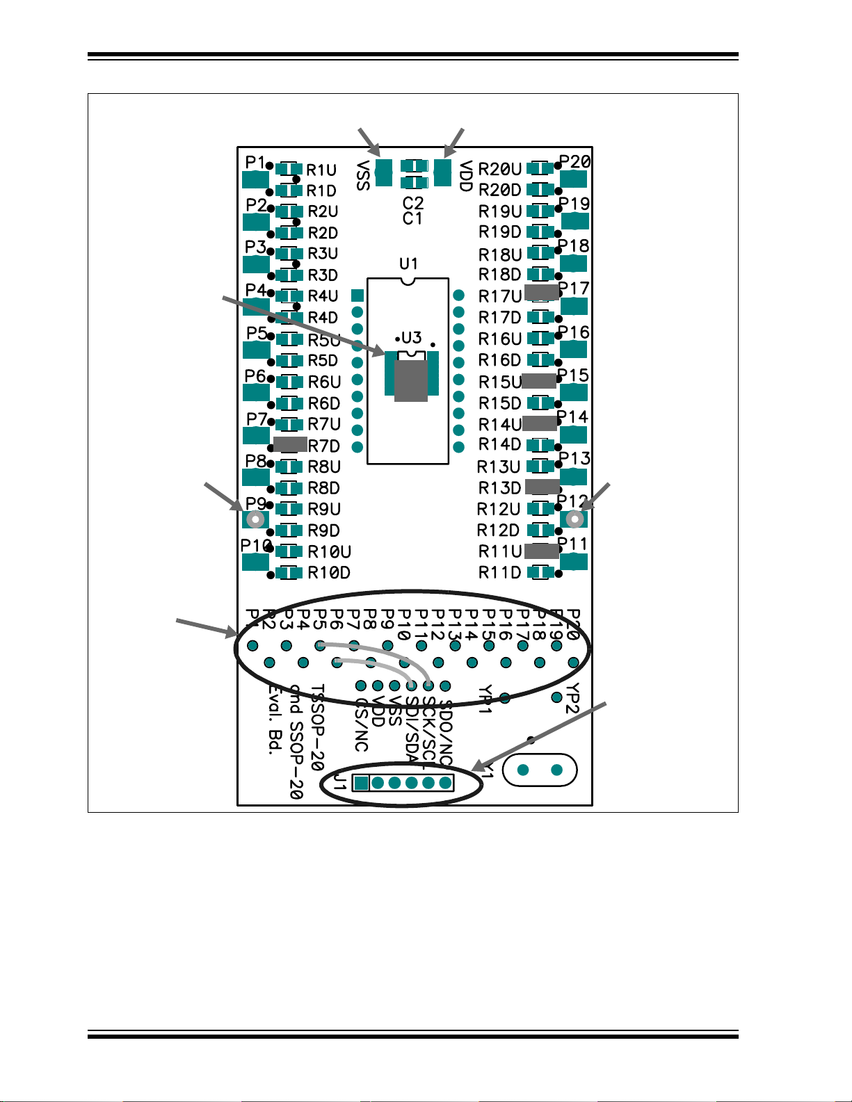
MCP46XXEV Evaluation Board User’s Guide
P1
P2
P9
PICkit™ Serial / ICSP™
Interface
J1
NC
NC
V
V
DD
VSS
SDI
SCK
SDO
DD
VSS
SDA
SCL
NC
DIP-20 (1)
1
2
9
10
20
19
12
11
P20
P19
P12
P11
Requires blue
wire jumpering
to connect the
™ Interface
PICkit
to the selected
device
P1
P2
P19
P10
TSSOP-20 (1)
20
1
19
2
V
V
DD
C1
P20
P12
SS
C2
SSOP-20
20
1
19
2
9
12
10
11
P1
P9
P2
P10
VIA1
C3
9
10
12
11
XTAL
VIA2
C4
R
1U
R
1D
R
2U
R
2D
P19
P11
R
19U
R
19D
R
20U
P20
R
20D
PIC® Circuitry (bottom of PCB)
Note: The MCP46X1 device (TSSOP-14 footprint) will be bottom aligned to the TSSOP-20
footprint.
FIGURE 2-1: TSSOP20EV Evaluation Board Circuit.
DS51929A-page 14 © 2010 Microchip Technology Inc.
Page 15

Installation and Operation
MCP4661-103E/ST
Installed in U3 (TSSOP-14 package bottom aligned to TSSOP-20 footprint)
Connected to
Ground Plane
Connected to
Power Plane
0 Ω
Through hole Test
Point (Orange)
Wiper 1
0 Ω
4361
10kΩ
10kΩ
0 Ω
0 Ω
Through hole Test
Point (Orange)
Wiper 0
Two Blue Wire Jumpers to connect
PICkit™ Serial interface (I
2
C) to device pins 1x6 Male Header, with 90° right angle
FIGURE 2-2: MCP46XXEV Evaluation Board Component Placement Using the TSSOP20EV
Evaluation Board (Top).
© 2010 Microchip Technology Inc. DS51929A-page 15
Page 16

MCP46XXEV Evaluation Board User’s Guide
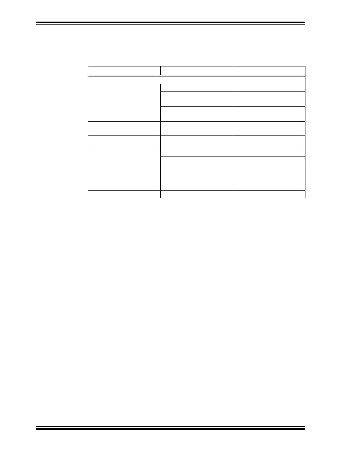
TABLE 2-1: INSTALLED PASSIVE COMPONENTS
Component Description Comment
R11U, R17U 0Ω SMT 805 Pull-up resistor
R14U, R15U 10 kΩ SMT 805 Pull-up resistor
R7D, R13D 0Ω SMT 805 Pull-down resistor
U3 MCP4661-103E/ST R
P9, P12 Test Point - through hole connector
(Orange)
J1 1x6 Male Header, 100 mil spacing 90°
angle.
— Blue Wire:
J1 SDI/SDA via to P6 via
J1 SCK/SCL via to P5 via
Note 1: Whichever pin is the device’s VDD pin, that corresponding RXD footprint can be used for the device’s
bypass capacitor. So if Pin 8 is the device’s V
2: All passive components use the surface mount 805 footprint.
(2)
(1)
= 10 kΩ
AB(TYP)
PICkit
™ Serial / ICSP™ header
Figure 2-2
See
pin, then install the bypass capacitor in the R8D footprint.
DD
DS51929A-page 16 © 2010 Microchip Technology Inc.
Page 17

Installation and Operation
TABLE 2-2: OPTIONAL PASSIVE COMPONENTS - NOT INSTALLED
(2)
Component Comment
C1, C2 Power supply bypass capacitors
(3)
C3, C4 PIC® MCU Crystal capacitors
R1U, R2U, R3U, R4U, R5U, R6U, R7U, R8U,
Pull-up resistor
R9U, R12U, R13U, R16U, R18U, R19U, R20U
R1D, R2D, R3D, R4D, R5D, R6D, R8D, R9D,
Pull-down resistor
(1)
R10D, R11D, R12D, R14D, R15D, R16D, R17D,
R18D, R19D, R20D
U1, U2 Alternate package footprints
VDD, GND Power and Ground plane connection
points
®
Y1 Can connect to either PIC
MCU’s main
oscillator or to the Timer oscillator circuit.
P1, P2, P3, P4, P5, P6, P8, P10, P11, P13, P14,
Test Point connectors
P15, P16, P17, P18, P19, P20
Note 1: Whichever pin is the device’s V
used for the device’s bypass capacitor. So if Pin 8 is the device’s V
pin, that corresponding RXD footprint can be
DD
pin, then
DD
install the by pass capacitor in the R8D footprint.
2: All passive components use the surface mount 805 footprint.
3: If the board is po w ered via the V
and GND connection points, the use of bypass
DD
capacitors on C1 and C2 may improve performance. The benefit is reduced if the
board is powered via the PICkit™ serial interface.
© 2010 Microchip Technology Inc. DS51929A-page 17
Page 18

MCP46XXEV Evaluation Board User’s Guide
2.4.2 The MCP4661 Device
T o make variations to the commands sent to the MCP4661 device (from the commands
shown in the demo section), one must know the device memory map (see Table 2-3)
and the command formats (see Figure 2-3 through Figure 2-5). For additional device
operational information, refer to the MCP4661 device data sheet (DS22107).
TABLE 2-3: MEMORY MAP AND THE SUPPORTED COMMANDS
).
Memory
Type
Allowed Commands
Increment, Decrement
Increment, Decrement
RAM Read, Write Increment, Decrement
pin to the VIH level and then back to the ac tive
Address Function
00h Volatile Wiper 0 RAM Read, Write,
01h Volatile Wiper 1 RAM Read, Write,
02h Non-Volatile Wiper 0 EEPROM Read, Write
03h Non-Volatile Wiper 1 EEPROM Read, Write
04h Volatile
TCON Register
05h Status Register RAM Read Write, Increment,
06h - 0Fh Data EEPROM EEPROM Read, Write
Note 1: When an EEPROM write is active, these are invalid commands and will generate
an error condition. The u ser shoul d use a rea d of the STATUS register to de termine
when the write cycle ha s co mpleted. To exit the error condition, the user must t ak e
pin to the VIH level and then back to the active state (VIL or V
the CS
2: This command on this address will generate an error condition. To exit the error
condition, the user must t ake the C S
state (V
IL
or V
IHH
Disallowed
Commands
—
—
(1)
Increment, Decrement
(1)
Increment, Decrement
Decrement
(1)
Increment, Decrement
).
IHH
(2)
Fixed
Address
Control Byte
Variable
Write bit
Address
1010SA2A1A00 0
Device
Memory
Address
ADADADAD
A0xD8AD3D7 D6 D5 D4 D2 D1 D0 A P
Command
0123
WRITE Command Write Data bits
FIGURE 2-3: MCP46XX I2C Single Write Command Format.
Write “Data” bits
DS51929A-page 18 © 2010 Microchip Technology Inc.
Page 19

Installation and Operation
Fixed
Address
Write bit
Device
Variable
Address
1010SA2A1A00 1
Memory
1
Command
0
Address
AD
ADADAD
A1xXASr
3
2
Repeated Start bit
Control Byte
READ Command
Read bit
1010 A2A1A01 A
00000 00D8A
Control Byte Read bits
Note 1: Master Device is responsible for A / A signal. If an A signal occurs, the MCP45XX/46XX will
abort this transfer and release the bus.
2: The Master Device will Not Acknowledge, and the MCP45XX/46XX will release the bus so the
Master Device can generate a Stop or Repeated Start condition.
3: The MCP45XX/46XX retains the last “Device Memory Address” that it has received. This is
the MCP45XX/46XX does not “corrup t” the “De vice Memory Address” af ter Repea ted Start or
Stop conditions.
FIGURE 2-4: MCP46XX I2C Single Read Command Format.
Fixed
Address
Control Byte
Fixed
Address
Variable
Write bit
Address
1010SA2A1A00 1
Write bit
Variable
Address
Device
Memory
1
Command
0
Address
AD
ADADAD
A0XXAP
23
STOP bit
DECR Command
Device
Memory
Address
Command
STOP bit
Read Data bits
1
STOP bit
D3D7 D6 D5 D4 D2 D1 D0 A
Command
Bits
C C
1 0
0 0 = Write Data
0 1 = INCR
1 0 = DECR
1 1 = Read Data
2
P
1010SA2A1A00 0
Control Byte
ADADADAD
A1xXAP
1
3
0
2
INCR Command
Note 1: Increment and De cre me nt Commands (INCR or DE CR ) onl y function when acce ss in g the
volatile wiper registers (AD3:AD0 = 0h and 1h).
FIGURE 2-5: MCP46XX I2C Single Increment / Decrement Command Format.
© 2010 Microchip Technology Inc. DS51929A-page 19
Page 20

MCP46XXEV Evaluation Board User’s Guide
2.5 CONFIGURING THE PICkit™ SERIAL ANALYZER
2.5.1 Modifying the “CommScripts.txt” file
Example 2-1 shows the User Scripts that need to be added to the PICkit serial’s
CommScripts.txt file. The default install location of this file is:
C:\Program Files\Microchip\PICkit Serial Analyzer
Once these are saved in the CommScripts.txt file and the Master SPI mode is
selected as the communication mode, these User Scripts will be available to select
from.
NOTICE
Note 1: It is recommended that you make a backup of your CommScripts.txt
file before making any edits with a text editor.
2: It has been observed that copying the text from this PDF and pasting into
the PICkit serial’ s CommScripts.txt file will cause errors due to the
blank spacing used in the PDF file. Please copy from the MCP46XX
CommScript.txt file available from the Microchip web site
(MCP46XXEV Evaluation Board Product Page).
EXAMPLE 2-1: MCP46XX SCRIPT FILE (COMMSCRIPTS.TXT)
MCP4661W0WR I2C I2CSTART I2CWRTBYT 0x03 0x5E 0x00 0x7F I2CSTOP
MCP4661W1WR I2C I2CSTART I2CWRTBYT 0x03 0x5E 0x10 0x7F I2CSTOP
MCP4661NVW0WR I2C I2CSTART I2CWRTBYT 0x03 0x5E 0x20 0x7F I2CSTOP
MCP4661NVW1WR I2C I2CSTART I2CWRTBYT 0x03 0x5E 0x30 0x7F I2CSTOP
MCP4661TCON0WR I2C I2CSTART I2CWRTBYT 0x03 0x5E 0x40 0x7F I2CSTOP
MCP4661EEWR I2C I2CSTART I2CWRTBYT 0x03 0x5E 0x60 0x7F I2CSTOP
MCP4661W0RD I2C I2CSTART I2CWRTBYT 0x02 0x5E 0x0C I2CRESTART I2CWRTBYT
0x01 0x5F I2CRDBYTNLB 0x02 I2CSTOP
MCP4661W1RD I2C I2CSTART I2CWRTBYT 0x02 0x5E 0x1C I2CRESTART I2CWRTBYT
0x01 0x5F I2CRDBYTNLB 0x02 I2CSTOP
MCP4661NVW0RD I2C I2CSTART I2CWRTBYT 0x02 0x5E 0x2C I2CRESTART I2CWRTBYT
0x01 0x5F I2CRDBYTNLB 0x02 I2CSTOP
MCP4661NVW1RD I2C I2CSTART I2CWRTBYT 0x02 0x5E 0x3C I2CRESTART I2CWRTBYT
0x01 0x5F I2CRDBYTNLB 0x02 I2CSTOP
MCP4661TCON0RD I2C I2CSTART I2CWRTBYT 0x02 0x5E 0x4C I2CRESTART I2CWRTBYT
0x01 0x5F I2CRDBYTNLB 0x02 I2CSTOP
MCP4661STATUSRD I2C I2CSTART I2CWRTBYT 0x02 0x5E 0x5C I2CRESTART I2CWRTBYT
0x01 0x5F I2CRDBYTNLB 0x02 I2CSTOP
MCP4661EERD I2C I2CSTART I2CWRTBYT 0x02 0x5E 0x6C I2CRESTART I2CWRTBYT
0x01 0x5F I2CRDBYTNLB 0x02 I2CSTOP
MCP4661W0INC I2C I2CSTART I2CWRTBYT 0x03 0x5E 0x04 0x7F I2CSTOP
MCP4661W0DEC I2C I2CSTART I2CWRTBYT 0x03 0x5E 0x08 0x7F I2CSTOP
DS51929A-page 20 © 2010 Microchip Technology Inc.
Page 21

Installation and Operation
2.5.2 Working With the PICkit™ Serial Analyzer
Figure 2-6 shows the PICkit Serial Window after the program has started. The
Transaction window indicates if the PICkit Serial GUI located the PICkit Serial Analyzer
hardware. When starting the PICkit Serial Analyzer for the first time, some setup
questions may be asked. If you have any questions, please refer to the PICkit Serial
Analyzer documentation, available at www.Microchip.com/PICkitSerial
.
FIGURE 2-6: PICkit™ Serial Main Window at Startup.
© 2010 Microchip Technology Inc. DS51929A-page 21
Page 22

MCP46XXEV Evaluation Board User’s Guide
We need to select the PICkit Serial Analyzer GUI to be in I2C Master mode. Figure 2-7
shows how to select the proper mode. Select PICkit Serial Analyzer -> Select
Communications Mode -> I2C Master menu item (make sure the I2C Master item is
checked).
FIGURE 2-7: PICkit™ Serial Selecting Communications Mode.
DS51929A-page 22 © 2010 Microchip Technology Inc.
Page 23
Installation and Operation
Now we need to configure the mode that we selected. Figure 2-8 shows how to open
the Communications Mode window. Select PICkit Serial Analyzer -> Configure
Communications Mode menu item. This will open a new window:
FIGURE 2-8: PICkit™ Serial - Opening the Communications Mode Window.
© 2010 Microchip Technology Inc. DS51929A-page 23
Page 24
MCP46XXEV Evaluation Board User’s Guide
Figure 2-9 shows the Configure Communications Mode window in Basic view while
Figure 2-10 shows the Configure Communications Mode window in Advanced view.
Ensure that your window options and settings are the same as this window, and then
select the Save Changes button. The Configure Communications Mode window may
now be closed. Ensure that the pull-ups are enabled, the board is powered if necessary,
and the desired I2CM bit rate has been selected.
FIGURE 2-9: PICkit™ Serial Configure Communications Mode window - Basic View.
DS51929A-page 24 © 2010 Microchip Technology Inc.
Page 25

Installation and Operation
FIGURE 2-10: PICkit™ Serial Configure Communications Mode window - Advanced View.
© 2010 Microchip Technology Inc. DS51929A-page 25
Page 26

MCP46XXEV Evaluation Board User’s Guide
Now we are going to open the Script Builder window, select the Communications ->
Script -> Script Builder menu item (see Figure 2-11).
FIGURE 2-11: PICkit™ Serial - Script Builder Menu Selection.
DS51929A-page 26 © 2010 Microchip Technology Inc.
Page 27

Installation and Operation
The Script Builder window is shown in Figure 2-12. In this window we see the User
I2CM Scripts including the ones that were added to the CommScripts.txt file.
FIGURE 2-12: PICkit Serial Script Builder Window.
© 2010 Microchip Technology Inc. DS51929A-page 27
Page 28

MCP46XXEV Evaluation Board User’s Guide
Double clicking on the MCP4661W0WR User I2CM Script will load the script details.
Figure 2-13 shows what the values mean in the Script Details. These values are hex
numbers.
The first value (03h), is the number of bytes that will be written. The second byte (5Eh)
is the MCP4661 I2C Slave Address with the R/W bit indicating a write (‘0’). The third
byte (00h) is a data byte and contains the Device Register Address, the Device
Command, and the two Most Significant bits (MSb) of the write data. The fourth byte
(7Fh) is the 2nd data byte and contains the remaining 8 bits of the write data.
Data Byte #1
(Device Slave Address + R/W bit)
Data Byte #2 Data Byte #3
(Device Register Address + (Write Data “D7:D0”)
Command + Data bit “D8”)
Number of Bytes that will
be written
FIGURE 2-13: Example Write Script.
DS51929A-page 28 © 2010 Microchip Technology Inc.
Page 29

Installation and Operation
Double clicking on the MCP4661W0RD User I2CM Script will load the script details.
Figure 2-14 shows what the values mean in the Script Details. These values are hex
numbers.
The first value (02h), is the number of bytes that will be written. The second byte (5Eh)
is the MCP4661 I2C Slave Address with the R/W bit indicating a write (0). The third byte
(0Ch) a data byte and contains the Device Register Address, the Device Command,
and the two Most Significant bits (MSb) of the write data.
2
The I
C protocol now has a restart bit. So the first value (01h) is the number of bytes
that will be written. The second byte (5Fh) is the MCP4661 I2C Slave Address with the
R/W bit indicating a read (1). The last byte (02h) is the number of bytes that will be read.
Data Byte #1
(Device Slave Address + R/W bit)
# of Bytes that
will be written
Data Byte #3
(Device Slave Address + R/W bit)
# of Bytes that
will be written
Data Byte #2
(Device Address +
Command + Data bit “D8”)
# of Bytes that
will be read
FIGURE 2-14: Example Read Script.
© 2010 Microchip Technology Inc. DS51929A-page 29
Page 30

MCP46XXEV Evaluation Board User’s Guide
2.6 MCP4661 DEMO STEPS
This demo assumes that you know how to configure the PICkit Serial Analyzer for
Master I
2
C operation. See Section 2.5 “Configuring The PICkit™ Seria l Analyzer”
or the “PICkit Serial Analyzer User’s Guide” (DS51647) for additional information.
1. Plug the PICkit serial device into the PC’s USB port.
2. Plug the MCP46XXEV Evaluation Board into the PICkit serial.
3. Add the User Scripts (see Example 2-1) to the CommScripts.TXT file.
4. Start the PICkit serial GUI.
5. Ensure the GUI is in Master I
6. Ensure that the Master I
2
C communication mode (see Figure 2-7).
2
C configuration is appropriately configured (see
Figure 2-9).
7. Measure the Wiper 0 voltage on the MCP46XXEV Evaluation Board (see
Figure 2-2) using an oscilloscope or digital multimeter. Measure voltage from the
ground plane (GND) to the wiper (P12). The voltage on the wiper should be ~
V
/2 (~2.5V).
DD
8. Open the Script Builder window (see Figure 2-11).
9. Double click on the “MCP4661W0WR” script in the “Example I2CM Scripts
column. This loads the Script Detail column (see Figure 2-13).
10. Click on the Execute Script button. This executes the script shown in the Script
Detail column, which will update the wiper value to 7Fh. The wiper voltage will
now be ~V
/2 (~2.5V).
DD
11. Select the “MCP4661W0RD” script in the User I2CM Scripts column. It should
look like Figure 2-14.
12. Click on the Execute Script button. This executes the script shown in the Script
Detail column. The Transaction window (see Figure 2-17) will be updated to
indicate the execution of the script.
13. Double click on the “MCP4661W0WR” script in the Example I2CM Scripts
column. This loads the Script Detail column (see Figure 2-13). Modify the fourth
byte to FF (see Figur e2-15).
14. Click on the Execute Script button. This executes the script shown in the Script
Detail column, which will update the wiper value to FFh. The wiper voltage will
now be ~V
(~5.0V).
DD
15. Select the “MCP4661W0RD ” script in the Use r I2CM Sc ripts column . It should
look like Figure 2-14.
16. Click on the Execute Script button. This executes the script shown in the Script
Detail column. The Transaction window (see Figure 2-17) will be updated to
indicate the execution of the script.
17. Double click on the “MCP4661W0WR” script in the Example I2CM Scripts
column. This loads the Script Detail column (see Figure 2-13). Modify the fourth
byte to 3F (see Figure 2-15).
18. Click on the Execute Script button. This executes the script shown in the Script
Detail column, which will update the wiper value to 3Fh. The wiper voltage will
now be ~V
/4 (~1.25V).
DD
19. Select the “MCP4661W0RD ” script in the Use r I2CM Sc ripts column . It should
look like Figure 2-14.
20. Click on the Execute Script button. This executes the script shown in the Script
Detail column. The Transaction window (see Figure 2-17) will be updated to
indicate the execution of the script.
21. In the Transaction window, click the Clear button.
DS51929A-page 30 © 2010 Microchip Technology Inc.
Page 31

Installation and Operation
22. On the PICkit Serial Analyzer command bar, click the Reset button.
23. Select the “MCP4661W0WR” script in the User I2CM Scripts column and then
click on the Execute Script button.
24. Select the “MCP4661W0RD ” script in the Use r I2CM Sc ripts column and then
click on the Execute Script button.
25. Select the “MCP4661W0DEC” script in the User I2CM Scripts column and then
click on the Execute Script button three times.
26. Select the “MCP4661W0RD ” script in the Use r I2CM Sc ripts column and then
click on the Execute Script button. The Transaction window shows the scripts
that were executed and the current value of the Wiper 0 (see Figure 2-18).
27. In the Transaction window, click the Clear button.
28. On the PICkit Serial Analyzer command bar, click the Reset button.
29. Select the “MCP4661W0WR” script in the User I2CM Scripts column and then
click on the Execute Script button.
30. Select the “MCP4661W0RD ” script in the Use r I2CM Sc ripts column and then
click on the Execute Script button.
31. Select the “MCP4661W0INC” script in the User I2CM Scripts column and then
click on the Execute Script button three times.
32. Select the “MCP4661W0RD ” script in the Use r I2CM Sc ripts column and then
click on the Execute Script button. The Transaction window shows the scripts
that were executed and the current value of the Wiper 0 (see Figure 2-19).
33. Y ou can repeat the sequence of writing values to the wiper register or writing then
reading the values back.
NOTICE
If at any time during script execution, an error message is generated in the transaction
window, it is good practice to reset the PICkit™ Serial Analyzer (PKSA). The PKSA can
be reset using the “Reset” toolbar icon. Verify that subsequent script operations do not
generate errors.
© 2010 Microchip Technology Inc. DS51929A-page 31
Page 32

MCP46XXEV Evaluation Board User’s Guide
Device Slave Address
+ R/W bit
FIGURE 2-15: MCP46XX Write Wiper 0 Script File - Wiper Value = 0FFh.
Device Slave Address
+ R/W bit
Write Command to Wiper 0
Register (D8 = ‘0’)
Write Command to Wiper 0
Register (D8 = ‘0’)
Wiper 0 Data
(D7:D0 = ‘FFh’)
Wiper 0 Data
(D7:D0 = ‘3Fh’)
FIGURE 2-16: MCP46XX Write Wiper 0 Script File - Wiper Value = 03Fh.
DS51929A-page 32 © 2010 Microchip Technology Inc.
Page 33

9-bit data value (07Fh)
written to
Wiper 0 register
9-bit data value (0FFh)
written to
Wiper 0 register
9-bit data value (03Fh)
written to
Wiper 0 register
Installation and Operation
9-bit dat a value (07Fh)
read from
Wiper 0 register
Wiper 0 register
read from
9-bit data value (0FFh)
Wiper 0 register
read from
9-bit data value (03Fh)
FIGURE 2-17: MCP4661 Transaction Window - Wiper 0 Writes and Reads.
Data value (07Fh) read
from Wiper 0 register
Data value (07Ch) read from Wiper 0 register after 3 Decrement Commands
FIGURE 2-18: MCP4661 Transaction Window - Wiper 0 Decrements.
© 2010 Microchip Technology Inc. DS51929A-page 33
Page 34

MCP46XXEV Evaluation Board User’s Guide
Data value (07Fh) read
from Wiper 0 register
Data value (082h) read from Wiper 0 register after 3 Increment Commands
FIGURE 2-19: MCP4661 Transaction Window - Wiper 0 Increments.
2.6.1 The TSSOP20EV PCB and Supported Digital Potentiometers
Table 2-4 shows the current digital potentiomers that are supported by the
TSSOP20EV PCB.
TABLE 2-4: TSSOP20EV PCB SUPPORTED DIGITAL POTENTIOMETERS
Device TSSOP-20 TSSOP-14 Comment
MCP4231 — Yes Dual Pot, SPI Interface
MCP4241 — Yes Dual Pot, SPI Interface
MCP4251 — Yes Dual Pot, SPI Interface
MCP4261 — Yes Dual Pot, SPI Interface
MCP4331 Yes — Quad Pot, SPI Interface
MCP4341 Yes — Quad Pot, SPI Interface
MCP4351 Yes — Quad Pot, SPI Interface
MCP4361 Yes — Quad Pot, SPI Interface
MCP4631 — Yes Dual Pot, I
MCP4641 — Yes Dual Pot, I
MCP4651 — Yes Dual Pot, I
MCP4661 — Yes Dual Pot, I
MCP42010 — Yes Dual Pot, SPI Interface
MCP42050 — Yes Dual Pot, SPI Interface
MCP42100 — Yes Dual Pot, SPI Interface
2
C™ Interface
2
C™ Interface
2
C™ Interface
2
C™ Interface
DS51929A-page 34 © 2010 Microchip Technology Inc.
Page 35

MCP46XXEV EVALUATION BOARD
Appendix A. Schematic and Layouts
A.1 INTRODUCTION
This appendix contains the schematics and layouts for the MCP46XXEV Evaluation
Board. Diagrams included in this appendix:
• Board – Schematic
• Board – Top Trace, Silk and Pads
• Board – Bottom Trace and Pads
• Board – Layer 2 Ground Plane
• Board – Layer 3 Power Plane
• Board Layout – Top Components
• Board – Bottom Silk, Trace and Pads
A.2 SCHEMATICS AND PCB LAYOUT
Board – Schematic shows the schematic of the MCP46XXEV Evaluation Board. The
layer order is shown in Figure A-1.
USER’S GUIDE
FIGURE A-1: Layer Order.
Top Layer
Ground Layer
Power Layer
Bottom Layer
© 2010 Microchip Technology Inc. Draft DS51929A-page 35
Page 36
MCP46XXEV Evaluation Board User’s Guide
A.3 BOARD – SCHEMATIC
M
DS51929A-page 36 Draft © 2010 Microchip Technology Inc.
Page 37
A.4 BOARD – TOP TRACE, SILK AND PADS
Schematic and Layouts
© 2010 Microchip Technology Inc. Draft DS51929A-page 37
Page 38
MCP46XXEV Evaluation Board User’s Guide
A.5 BOARD – BOTTOM TRACE AND PADS
DS51929A-page 38 Draft © 2010 Microchip Technology Inc.
Page 39

A.6 BOARD – LAYER 2 GROUND PLANE
Schematic and Layouts
© 2010 Microchip Technology Inc. Draft DS51929A-page 39
Page 40

MCP46XXEV Evaluation Board User’s Guide
A.7 BOARD – LAYER 3 POWER PLA N E
DS51929A-page 40 Draft © 2010 Microchip Technology Inc.
Page 41

A.8 BOARD LAYOUT – TOP COMPONENTS
Schematic and Layouts
© 2010 Microchip Technology Inc. Draft DS51929A-page 41
Page 42

MCP46XXEV Evaluation Board User’s Guide
A.9 BOARD – BOTTOM SILK, TRACE AND PADS
DS51929A-page 42 Draft © 2010 Microchip Technology Inc.
Page 43

MCP46XXEV EVALUATION BOARD
USER’S GUIDE
Appendix B. Bill of Materials (BOM)
TABLE B-1: BILL OF MATERIALS
Qty Reference Description Manufacturer Part Number
1 J1 CONN HEADER 6POS .100 R/A TIN Molex/Waldom
Electronics Corp
2 P9, P12 TEST POINT PC MULTI PURPOSE
THROUGH HOLE (Orange)
1PCB Note 1 Microchip T e chnology
2 R14U, R15U RES 10K OHM 1/8W 5% 0805 SMD Panasonic - ECG ERJ-6GEYJ103V
4 R7D, R11U,
R13D, R17U
1 U3 MCP4661 10 kOhm Digital Potentiometer
Note 1: This assembly uses RoHS Compliant TSSOP-20 to DIP-20 Evaluation Board.
2: The components listed in this Bill of Ma terials are re pre sentat ive o f th e PCB as sembl y. The released BOM
used in manufacturing uses all RoHS-compliant components.
RES 0.0 OHM 1/8W 5% 0805 SMD Panasonic
device. Device bottom aligned in U3
footprint (See Asembly Drawing) .
Keystone
Electronics
Inc.
Microchip T ech nology
Inc.
®
®
- ECG ERJ-6GEY0R00V
22-05-2061
5013
104-00272
MCP4261-103E/ST
© 2010 Microchip Technology Inc. Draft DS51929A-page 43
Page 44

WORLDWIDE SALES AND SERVICE
AMERICAS
Corporate Office
2355 West Chandler Blvd.
Chandler, AZ 85224-6199
Tel: 480-792-7200
Fax: 480-792-7277
Technical Support:
http://support.microchip.com
Web Address:
www.microchip.com
Atlanta
Duluth, GA
Tel: 678-957-9614
Fax: 678-957-1455
Boston
Westborough, MA
Tel: 774-760-0087
Fax: 774-760-0088
Chicago
Itasca, IL
Tel: 630-285-0071
Fax: 630-285-0075
Cleveland
Independence, OH
Tel: 216-447-0464
Fax: 216-447-0643
Dallas
Addison, TX
Tel: 972-818-7423
Fax: 972-818-2924
Detroit
Farmington Hills, MI
Tel: 248-538-2250
Fax: 248-538-2260
Kokomo
Kokomo, IN
Tel: 765-864-8360
Fax: 765-864-8387
Los Angeles
Mission Viejo, CA
Tel: 949-462-9523
Fax: 949-462-9608
Santa Clara
Santa Clara, CA
Tel: 408-961-6444
Fax: 408-961-6445
Toronto
Mississauga, Ontario,
Canada
Tel: 905-673-0699
Fax: 905-673-6509
ASIA/PACIFIC
Asia Pacific Office
Suites 3707-14, 37th Floor
Tower 6, The Gateway
Harbour City, Kowloon
Hong Kong
Tel: 852-2401-1200
Fax: 852-2401-3431
Australia - Sydney
Tel: 61-2-9868-6733
Fax: 61-2-9868-6755
China - Beijing
Tel: 86-10-8528-2100
Fax: 86-10-8528-2104
China - Chengdu
Tel: 86-28-8665-5511
Fax: 86-28-8665-7889
China - Chongqing
Tel: 86-23-8980-9588
Fax: 86-23-8980-9500
China - Hong Kong SAR
Tel: 852-2401-1200
Fax: 852-2401-3431
China - Nanjing
Tel: 86-25-8473-2460
Fax: 86-25-8473-2470
China - Qingdao
Tel: 86-532-8502-7355
Fax: 86-532-8502-7205
China - Shanghai
Tel: 86-21-5407-5533
Fax: 86-21-5407-5066
China - Shenyang
Tel: 86-24-2334-2829
Fax: 86-24-2334-2393
China - Shenzhen
Tel: 86-755-8203-2660
Fax: 86-755-8203-1760
China - Wuhan
Tel: 86-27-5980-5300
Fax: 86-27-5980-5118
China - Xian
Tel: 86-29-8833-7252
Fax: 86-29-8833-7256
China - Xiamen
Tel: 86-592-2388138
Fax: 86-592-2388130
China - Zhuhai
Tel: 86-756-3210040
Fax: 86-756-3210049
ASIA/PACIFIC
India - Bangalore
Tel: 91-80-3090-4444
Fax: 91-80-3090-4123
India - New Delhi
Tel: 91-11-4160-8631
Fax: 91-11-4160-8632
India - Pune
Tel: 91-20-2566-1512
Fax: 91-20-2566-1513
Japan - Yokohama
Tel: 81-45-471- 6166
Fax: 81-45-471-6122
Korea - Daegu
Tel: 82-53-744-4301
Fax: 82-53-744-4302
Korea - Seoul
Tel: 82-2-554-7200
Fax: 82-2-558-5932 or
82-2-558-5934
Malaysia - Kuala Lumpur
Tel: 60-3-6201-9857
Fax: 60-3-6201-9859
Malaysia - Penang
Tel: 60-4-227-8870
Fax: 60-4-227-4068
Philippines - Manila
Tel: 63-2-634-9065
Fax: 63-2-634-9069
Singapore
Tel: 65-6334-8870
Fax: 65-6334-8850
Tai wan - Hsin Chu
Tel: 886-3-6578-300
Fax: 886-3-6578-370
Taiwan - Kaohsiung
Tel: 886-7-213-7830
Fax: 886-7-330-9305
Taiwan - Taipei
Tel: 886-2-2500-6610
Fax: 886-2-2508-0102
Thailand - Bangkok
Tel: 66-2-694-1351
Fax: 66-2-694-1350
EUROPE
Austria - Wels
Tel: 43-7242-2244-39
Fax: 43-7242-2244-393
Denmark - Copenhagen
Tel: 45-4450-2828
Fax: 45-4485-2829
France - Paris
Tel: 33-1-69-53-63-20
Fax: 33-1-69-30-90-79
Germany - Munich
Tel: 49-89-627-144-0
Fax: 49-89-627-144-44
Italy - Milan
Tel: 39-0331-742611
Fax: 39-0331-466781
Netherlands - Drunen
Tel: 31-416-690399
Fax: 31-416-690340
Spain - Madrid
Tel: 34-91-708-08-90
Fax: 34-91-708-08-91
UK - Wokingham
Tel: 44-118-921-5869
Fax: 44-118-921-5820
08/04/10
DS51929A-page 44 © 2010 Microchip Technology Inc.
 Loading...