

Page 1

MCP401X/2X
Digital Potentiometer
Evaluation Board
User’s Guide
© 2005 Microchip Technology Inc. DS51546B
Page 2
Note the following details of the code protection feature on Microchip devices:
• Microchip products meet the specification contained in their particular Microchip Data Sheet.
• Microchip believes that its family of products is one of the most secure families of its kind on the market today, when used in the
intended manner and under normal conditions.
• There are dishonest and possibly illegal methods used to breach the code protection feature. All of these methods, to our
knowledge, require using the Microchip products in a manner outside the operating specifications contained in Microchip’s Data
Sheets. Most likely, the person doing so is engaged in theft of intellectual property.
• Microchip is willing to work with the customer who is concerned about the integrity of their code.
• Neither Microchip nor any other semiconductor manufacturer can guarantee the security of their code. Code protection does not
mean that we are guaranteeing the product as “unbreakable.”
Code protection is constantly evolving. We at Microchip are committed to continuously improving the code protection features of our
products. Attempts to break Microchip’s code protection feature may be a violation of the Digital Millennium Copyright Act. If such acts
allow unauthorized access to your software or other copyrighted work, you may have a right to sue for relief under that Act.
Information contained in this publication regarding device
applications and the like is provided only for your convenience
and may be superseded by updates. It is your responsibility to
ensure that your application meets with your specifications.
MICROCHIP MAKES NO REPRESENTATIONS OR WARRANTIES OF ANY KIND WHETHER EXPRESS OR IMPLIED,
WRITTEN OR ORAL, STATUTORY OR OTHERWISE,
RELATED TO THE INFORMATION, INCLUDING BUT NOT
LIMITED TO ITS CONDITION, QUALITY, PERFORMANCE,
MERCHANTABILITY OR FITNESS FOR PURPOSE.
Microchip disclaims all liability arising from this information and
its use. Use of Microchip’s products as critical components in
life support systems is not authorized except with express
written approval by Microchip. No licenses are conveyed,
implicitly or otherwise, under any Microchip intellectual property
rights.
Trademarks
The Microchip name and logo, the Microchip logo, Accuron,
dsPIC, K
EELOQ, microID, MPLAB, PIC, PICmicro, PICSTART,
PRO MATE, PowerSmart, rfPIC, and SmartShunt are
registered trademarks of Microchip Technology Incorporated
in the U.S.A. and other countries.
AmpLab, FilterLab, Migratable Memory, MXDEV, MXLAB,
PICMASTER, SEEVAL, SmartSensor and The Embedded
Control Solutions Company are registered trademarks of
Microchip Technology Incorporated in the U.S.A.
Analog-for-the-Digital Age, Application Maestro, dsPICDEM,
dsPICDEM.net, dsPICworks, ECAN, ECONOMONITOR,
FanSense, FlexROM, fuzzyLAB, In-Circuit Serial
Programming, ICSP, ICEPIC, Linear Active Thermistor,
MPASM, MPLIB, MPLINK, MPSIM, PICkit, PICDEM,
PICDEM.net, PICLAB, PICtail, PowerCal, PowerInfo,
PowerMate, PowerTool, rfLAB, rfPICDEM, Select Mode,
Smart Serial, SmartTel, Total Endurance and WiperLock are
trademarks of Microchip Technology Incorporated in the
U.S.A. and other countries.
SQTP is a service mark of Microchip Technology Incorporated
in the U.S.A.
All other trademarks mentioned herein are property of their
respective companies.
© 2005, Microchip Technology Incorporated, Printed in the
U.S.A., All Rights Reserved.
Printed on recycled paper.
Microchip received ISO/TS-16949:2002 quality system certification for
its worldwide headquarters, design and wafer fabrication facilities in
Chandler and Tempe, Arizona and Mountain View, California in
October 2003. The Company’s quality system processes and
procedures are for its PICmicro
devices, Serial EEPROMs, microperipherals, nonvolatile memory and
analog products. In addition, Microchip’s quality system for the design
and manufacture of development systems is ISO 9001:2000 certified.
®
8-bit MCUs, KEEL
®
OQ
code hopping
DS51546B-page ii © 2005 Microchip Technology Inc.
Page 3

MCP401X/2X EVALUATION
BOARD USER’S GUIDE
Tabl e of Conten ts
Preface ........................................................................................................................... 1
Chapter 1. Product Overview
1.1 Introduction ..................................................................................................... 5
1.2 What is the MCP402X Digital Potentiometer Evaluation Board? ................... 5
1.3 What the MCP402X Digital Potentiometer Evaluation Board Kit Includes ..... 6
Chapter 2. Installation and Operation
2.1 Introduction ..................................................................................................... 7
2.2 PCB Description ............................................................................................. 7
2.3 Test and Operating Instructions ................................................................... 10
2.4 Firmware Description ................................................................................... 17
Appendix A. Schematic and Layouts
A.1 Introduction .................................................................................................. 19
A.2 Schematic .................................................................................................. 20
A.3 MCP402X Board Layout – Top Layer + Silk-screen ................................. 21
A.4 MCP402X Board Layout – Bottom Layer ................................................. 21
A.5 MCP402X Board Layout – Top Silkscreen ............................................... 22
A.6 MCP402X Board Layout – Bottom Layer + Silk-screen ........................... 22
Appendix B. Bill Of Materials (BOM)
Appendix C. Using the BFMP Programmer to Power the Board
C.1 Powering the Board Using the BFMP Programmer ..................................... 25
Appendix D. Potential Programming Issue of the MCP402XEV
D.1 Introduction .................................................................................................. 27
Appendix E. 00066_MCP402XEV.ASM Source Code
E.1 Introduction .................................................................................................. 29
Worldwide Sales and Service .................................................................................... 42
© 2005 Microchip Technology Inc. DS51546B-page iii
Page 4

MCP401X/2X Evaluation Board User’s Guide
NOTES:
DS51546B-page iv © 2005 Microchip Technology Inc.
Page 5

MCP401X/2X EVALUATION
BOARD USER’S GUIDE
Preface
NOTICE TO CUSTOMERS
All documentation becomes dated, and this manual is no exception. Microchip tools and
documentation are constantly evolving to meet customer needs, so some actual dialogs
and/or tool descriptions may differ from those in this document. Please refer to our web site
(www.microchip.com) to obtain the latest documentation available.
Documents are identified with a “DS” number. This number is located on the bottom of each
page, in front of the page number. The numbering convention for the DS number is
“DSXXXXXA”, where “XXXXX” is the document number and “A” is the revision level of the
document.
INTRODUCTION
This chapter contains general information that will be useful to know before using the
MCP402X Digital Potentiometer Evaluation Board. Items discussed in this chapter
include:
• Document Layout
• Conventions Used in this Guide
• Recommended Reading
• The Microchip Web Site
• Customer Support
• Document Revision History
DOCUMENT LAYOUT
This document describes how to use the MCP402X Digital Potentiometer Evaluation
Board. The manual layout is as follows:
• Chapter 1. “Product Overview” – Important information about the MCP402X
Digital Potentiometer Evaluation Board.
• Chapter 2. “Installation and Operation” – Includes instructions on how to get
started with this evaluation board.
• Appendix A. “Schematic and Layouts” – Shows the schematic and layout
diagrams for the MCP402X Digital Potentiometer Evaluation Board.
• Appendix B. “Bill Of Materials (BOM)” – Lists the parts used to build the
MCP402X Digital Potentiometer Evaluation Board.
• Appendix C. “Using the BFMP Programmer to Power the Board” – Shows
how to interface the BFMP board with the MCP402X Digital Potentiometer Evaluation Board.
• Appendix D. “Potential Programming Issue of the MCP402XEV” – Discusses
possible programming issues with Rev 1 and Rev 2 of the MCP402X Digital
Potentiometer Evaluation Board.
• Appendix E. “00066_MCP402XEV.ASM Source Code” – Provides information
about the application firmware, as well as the location of the source code.
© 2005 Microchip Technology Inc. DS51546B-page 1
Page 6
MCP401X/2X Evaluation Board User’s Guide
CONVENTIONS USED IN THIS GUIDE
This manual uses the following documentation conventions:
DOCUMENTATION CONVENTIONS
Description Represents Examples
Arial font:
Italic characters Referenced books
Emphasized text ...is the
Initial caps A window the Output window
A dialog the Settings dialog
A menu selection select Enable Programmer
Quotes A field name in a window or
dialog
Underlined, italic text with
right angle bracket
Bold characters A dialog button Click OK
‘b
nnnn
Text in angle brackets < > A key on the keyboard Press <Enter>, <F1>
Courier New font:
Plain Courier New Sample source code #define START
Italic Courier New A variable argument file.o, where file can be
0xnnnn A hexadecimal number where
Square brackets [ ] Optional arguments mcc18 [options] file
Curly brackets and pipe
character: { | }
Ellipses... Replaces repeated text var_name [,
A menu path
A tab Click the Power tab
A binary number where n is a
digit
Filenames autoexec.bat
File paths c:\mcc18\h
Keywords _asm, _endasm, static
Command-line options -Opa+, -Opa-
Bit values 0, 1
n is a hexadecimal digit
Choice of mutually exclusive
arguments; an OR selection
Represents code supplied by
user
MPLAB® IDE User’s Guide
“Save project before build”
File>Save
‘b00100, ‘b10
any valid filename
0xFFFF, 0x007A
[options]
errorlevel {0|1}
var_name...]
void main (void)
{ ...
}
only
compiler...
RECOMMENDED READING
This user's guide describes how to use the MCP402X Digital Potentiometer Evaluation
Board. The following Microchip documents are available and recommended as
supplemental reference resources.
MCP4011/2/3/4,
(DS21978).
MCP4021/2/3/4,
Data Sheet (DS21945).
PIC10F200/202/204/206,
DS51546B-page 2 © 2005 Microchip Technology Inc.
“Low-Cost, 64-Step Volatile Digital POT in SOT-23”
Data Sheet
“Low-Cost NV Digital POT in SOT-23 with WiperLock™ Technology”
“6-Pin, 8-Bit Flash Microcontrollers”
Data Sheet (DS41239)
Page 7

THE MICROCHIP WEB SITE
Microchip provides online support via our web site at www.microchip.com. This web
site is used as a means to make files and information easily available to customers.
Accessible by using your favorite Internet browser, the web site contains the following
information:
• Product Support – Data sheets and errata, application notes and sample
programs, design resources, user’s guides and hardware support documents,
latest software releases and archived software
• General Technical Support – Frequently Asked Questions (FAQs), technical
support requests, online discussion groups, Microchip consultant program
member listing
• Business of Microchip – Product selector and ordering guides, latest Microchip
press releases, listing of seminars and events, listings of Microchip sales offices,
distributors and factory representatives
CUSTOMER SUPPORT
Users of Microchip products can receive assistance through several channels:
• Distributor or Representative
• Local Sales Office
• Field Application Engineer (FAE)
• Technical Support
• Development Systems Information Line
Customers should contact their distributor, representative or field application engineer
(FAE) for support. Local sales offices are also available to help customers. A listing of
sales offices and locations is included in the back of this document.
Technical support is available through the web site at: http://support.microchip.com
Preface
DOCUMENT REVISION HISTORY
Revision B (December 2005)
• Updated to include MCP401X devices
• Enhancement of Operation Description
• Added Appendix C. “Using the BFMP Programmer to Power the Board” -
Programming the MCP402X Digital Potentiometer Evaluation Board
• Added Appendix D. “Potential Programming Issue of the MCP402XEV”- A
description of potential programming issues (and their solutions) with the
MCP402X Digital Potentiometer Evaluation Board
Revision A (April 2005)
• Initial Release of this Document
© 2005 Microchip Technology Inc. DS51546B-page 3
Page 8

MCP401X/2X Evaluation Board User’s Guide
NOTES:
DS51546B-page 4 © 2005 Microchip Technology Inc.
Page 9

MCP401X/2X EVALUATION
BOARD USER’S GUIDE
Chapter 1. Product Overview
1.1 INTRODUCTION
This chapter provides an overview of the MCP402X Digital Potentiometer Evaluation
Board and covers the following topics:
• What is the MCP402X Digital Potentiometer Evaluation Board?
• What the MCP402X Digital Potentiometer Evaluation Board includes
1.2 WHAT IS THE MCP402X DIGITAL POTENTIOMETER EVALUATION BOARD?
The MCP402X Digital Potentiometer Evaluation Board (MCP402XEV) allows the
system designer to quickly evaluate the operation of Microchip Technology’s
MCP401X/2X Digital Potentiometer products.
The MCP402X Digital Potentiometer Evaluation Board PCB was designed to support:
• 8-pin, 150 mil SOIC MCP4021-XXX/SN devices
• SOT-23-6 MCP4022-XXX/OT devices
• SOT-23-6 MCP4023-XXX/OT devices
• SOT-23-5 MCP4024-XXX/OT devices
• 8-pin, 150 mil SOIC MCP4011-XXX/SN devices
• SOT-23-6 MCP4012-XXX/OT devices
• SOT-23-6 MCP4013-XXX/OT devices
• SOT-23-5 MCP4014-XXX/OT devices
In addition to supporting the MCP401X/2X, the MCP402XEV also utilizes the SOT-23-6
PIC10F20X microcontroller.
The PIC10F20X is supplied with example firmware that debounces the INCR and
DECR push buttons and generates the simple U/D
MCP401X/2X to increment and decrement the potentiometer’s wiper. It also generates
the simple U/D
potentiometer’s wiper.
protocol required by the MCP402X to lock and unlock the
protocol required by the
© 2005 Microchip Technology Inc. DS51546B-page 5
Page 10

MCP401X/2X Evaluation Board User’s Guide
1.3 WHAT THE MCP402X DIGITAL POTENTIOMETER EVALUATION BOARD KIT
INCLUDES
This MCP402X Digital Potentiometer Evaluation Board Kit includes:
• One populated Printed Circuit Board (PCB)
- MCP4021-103/OT
- PIC10F206-I/OT with 00066_MCP402XEV.HEX programmed into memory
- Two push button switches: one for Increment commands (INCR), one for
Decrement commands (DECR)
- Decoupling capacitors
- 5 resistors to isolate the switches and create a voltage divider with the
MCP4021-103/OT
• One blank PCB to allow rapid prototyping of a specific digital potentiometer
configuration
• 2 samples each of the MCP4021-202/OT, MCP4021-502/OT, MCP4021-103/OT
and MCP4021-503/OT
• 1 PIC10F20X-I/OT sample
• MCP401X/2X Digital Potentiometer Evaluation Board User’s Guide
(electronic version on CD) (DS51546)
DS51546B-page 6 © 2005 Microchip Technology Inc.
Page 11

Chapter 2. Installation and Operation
2.1 INTRODUCTION
The MCP402X Digital Potentiometer Evaluation Board provides a tested,
out-of-the-box example of a MCP401X/2X application. The circuit description is
described in Section 2.2 “PCB Description”, while the test and operating instructions
are described in Section 2.3 “Test and Operating Instructions”. A supplied blank
PCB allows rapid prototyping of the designer’s specific MCP401X/2X device, along
with other desired passive components (resistor and capacitors) and connection posts.
2.2 PCB DESCRIPTION
The MCP402X Digital Potentiometer Evaluation Board has the following features:
• 150 mil, 8-pin SOIC pinout (U1) supports the MCP4021 and MCP4011 devices
• SOT-23-6 pinout (U2) supports the MCP4022/23/24 and MCP4012/13/14 devices
• SOT-23-6 pinout (U3) supports the PIC10F20X devices
• Connection terminals can be left unpopulated for easy connection using small
alligator clip leads (clamped across the edge of the board) or populated with either
through-hole or surface-mount terminals
• Footprints for optional passive components for:
- Power supply filtering
- Device bypass capacitor
- Terminal “A” pull-up resistor
- Terminal “B” pull-down resistor
• Footprints for two switches:
- INCR button operation can be detected by the PIC10F20X to generate
Increment commands (move wiper toward terminal A)
- DECR button operation can be detected by the PIC10F20X to generate
Decrement commands (move wiper toward terminal B)
• Button sequence instructions are printed on the back of the PCB
Appendix A.2 “Schematic” illustrates the schematic for the MCP402XEV.
MCP401X/2X EVALUATION
BOARD USER’S GUIDE
Note: The PIC10F20X firmware (00066_MCP402XEV.HEX) must be
programmed into the microcontroller before the MCP402XEV is functional.
© 2005 Microchip Technology Inc. DS51546B-page 7
Page 12

MCP401X/2X Evaluation Board User’s Guide
2.2.1 Evaluating the MCP4021 and MCP4011
The MCP4021/11-XXXI/SN is an 8-pin digital potentiometer device with terminals A, B
and W available on the device pins. Footprint U1 supports the 150 mil SOIC package.
Resistors R2 and R3 are 2.5 k
MCP4021-103I/SN digital potentiometer. This creates a “windowed” voltage divider
with a transfer function illustrated in Equation 2-1.
EQUATION 2-1: WINDOWED POTENTIOMETER – VOLTAGE DIVIDER
CALCULATION
V
wiper
Note 1: DO NOT populate U2 if using U1.
2: The MCP4011 has high-voltage tolerant pins and, therefore, accepts
high-voltage Increment and Decrement commands. Since this device is
nonvolatile, the WiperLock™ Technology feature is not present.
Ω on the populated PCB, along with the 10 kΩ
V
DDRwb
------------------------------------------R2 R3 R
++
R3+()⋅
5.0V d 10k
---------------------------------------------------------------------
==
nom
⋅
()63⁄2.5k+()
⋅
2.5k 2.5k 10k++
Where:
d = the wiper setting (0 to 63)
2.2.2 Evaluating the MCP4022 and MCP4012
The MCP4022/12-XXXI/OT is a 6-pin, stand-alone digital rheostat with terminals A and
W available on the device pins. Footprint U2 supports the SOT-23-6 package. An
“INCR” command moves the wiper toward terminal A, thus causing the resistance
across the rheostat to decrease. A “DECR” command moves the wiper toward terminal
B, thus causing the resistance across the rheostat to increase.
Note 1: DO NOT populate U1 if using U2.
2: The included MCP4021 digital potentiometer samples could be used to
evaluate the MCP4022 simply by not populating R3 and letting terminal
B float.
3: The MCP4012 has high-voltage tolerant pins and, therefore, accepts
high-voltage Increment and Decrement commands. Since this device is
nonvolatile, the WiperLock™ Technology feature is not present.
DS51546B-page 8 © 2005 Microchip Technology Inc.
Page 13

Installation and Operation
2.2.3 Evaluating the MCP4023 and MCP4013
The MCP4023/13-XXXI/OT is a 6-pin, grounded digital potentiometer with terminals A
and W available on the device pins. Footprint U2 supports the SOT-23-6 package.
Populating R2 will create a voltage divider with a transfer function illustrated in
Equation 2-2.
EQUATION 2-2: GROUNDED POTENTIOMETER – VOLTAGE DIVIDER
CALCULATION
V
wiper
VDDRwb⋅
-------------------------R2 R
+
5.0V d 10k
-----------------------------------------------
==
nom
Where:
d = the wiper setting (0 to 63)
Note 1: DO NOT populate U1 if using U2.
2: The included MCP4021 digital potentiometer samples could be used to
evaluate the MCP4023 simply by shorting terminal B to GND.
3: The MCP4013 has high-voltage tolerant pins and, therefore, accepts
high-voltage Increment and Decrement commands. Since this device is
nonvolatile, the WiperLock™ Technology feature is not present.
⋅63⁄
()
⋅
2.5k 10k+
2.2.4 Evaluating the MCP4024 and MCP4014
The MCP4024/14-xxxI/OT is a 5-pin, grounded digital rheostat with the W terminals
available on the device pins. Footprint U2 supports the SOT-23-5 package. An “INCR”
command moves the wiper toward terminal A, thus causing the resistance across the
rheostat to increase. A “DECR” command moves the wiper toward terminal B, thus
causing the resistance across the rheostat to decrease.
Note 1: DO NOT populate U1 if using U2.
2: The included MCP4021 digital potentiometer samples could be used to
evaluate the MCP4024 simply by not populating R
float and by shorting terminal B to GND.
3: The MCP4014 has high-voltage tolerant pins and, therefore, accepts
high-voltage Increment and Decrement commands. Since this device is
nonvolatile, the WiperLock™ Technology feature is not present.
, letting terminal A
2
© 2005 Microchip Technology Inc. DS51546B-page 9
Page 14
MCP401X/2X Evaluation Board User’s Guide
2.3 TEST AND OPERATING INSTRUCTIONS
The populated PCB is configured to create a voltage divider from VDD to VSS using a
2.5 kΩ pull-up resistor (R2), the MCP4021-103I/SN (10 kΩ) and a 2.5 kΩ pull-down
resistor (R3). To quickly evaluate the digital potentiometer’s performance, the following
test equipment is required:
• 2.7V to 5.5V power supply
• Voltmeter or Digital Multimeter (DMM)
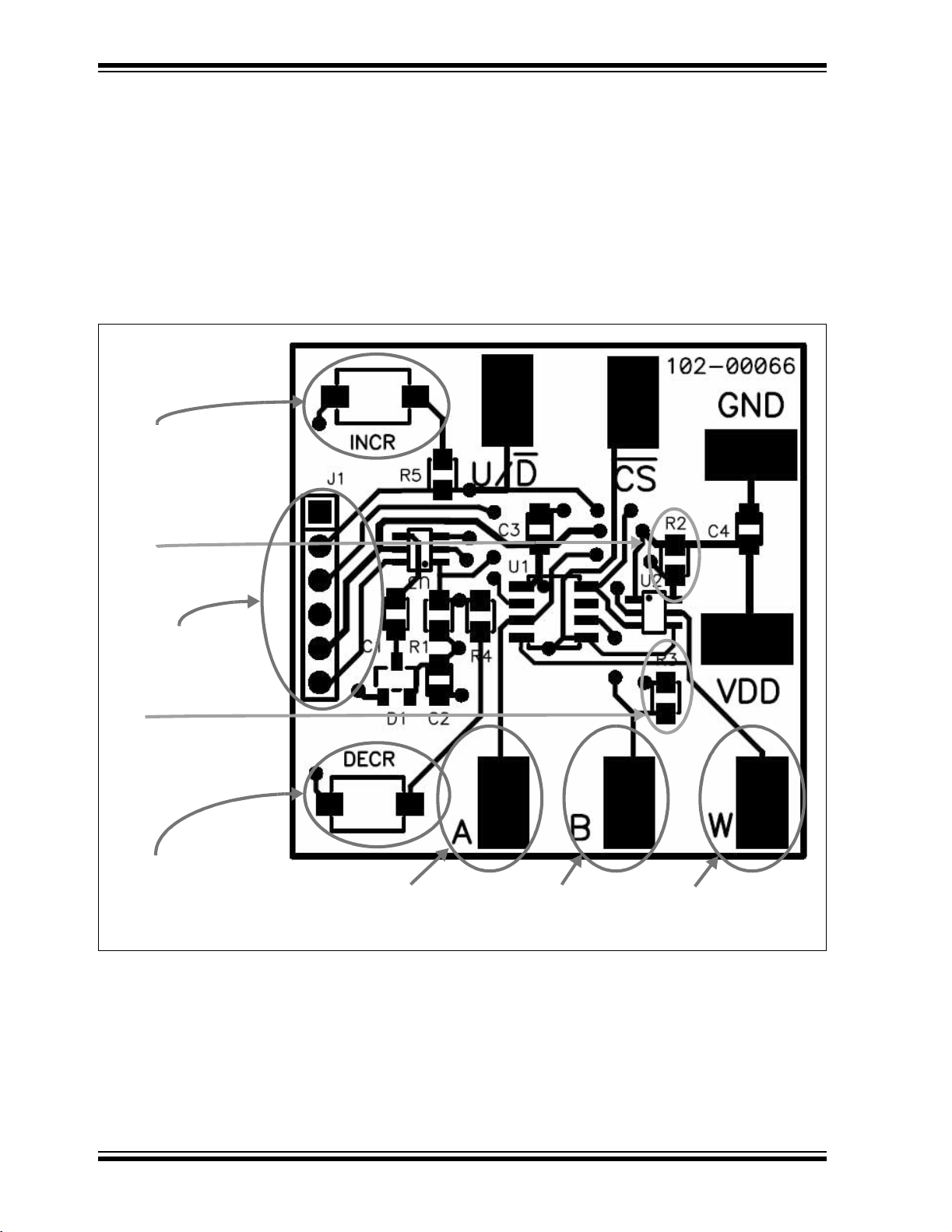
Figure 2-1 shows the Digital Potentiometer Evaluation Board PCB, components and
the connection points that will be used in the step-by-step demonstration.
Increment (INCR)
Switch
Resistor R2
(A to VDD)
Baseline Flash MCU
Programmer (BFMP)
Interface
Resistor R3
(B to GND)
Decrement (DECR)
Switch
FIGURE 2-1: Digital Potentiometer Evaluation Board Overview.
Digital
Potentiometer
Node A Pad
Digital
Potentiometer
Node B Pad
Digital
Potentiometer
Wiper W Pad
DS51546B-page 10 © 2005 Microchip Technology Inc.
Page 15

Installation and Operation
2.3.1 Test Setup
1. Connect the power supply “+” to VDD and the “–” to GND.
2. Connect the voltmeter to the W terminal and GND.
The voltmeter should reflect the wiper setting with respect to Equation 2-3.
EQUATION 2-3: POPULATED PCB – VOLTAGE DIVIDER CALCULATION
V
DDRwb
V
wiper
------------------------------------------R2 R 3 R
++
Where:
d = the wiper setting (0 to 63)
Using R2 and R3 = 2.5 kΩ:
• If a 2 kΩ MCP4021 is utilized, the output range will be approximately 1.79V to
3.21V.
• If a 5 kΩ MCP4021 is utilized, the output range will be approximately 1.25V to
3.75V.
• If a 10 kΩ MCP4021 is utilized, the output range will be approximately 0.83V to
4.17V.
• If a 50 kΩ MCP4021 is utilized, the output range will be approximately 0.23V to
4.77V.
R3+()⋅
5.0V d 10k
---------------------------------------------------------------------
==
AB
⋅
()63⁄2.5k+()
⋅
2.5k 2.5k 10k++
© 2005 Microchip Technology Inc. DS51546B-page 11
Page 16

MCP401X/2X Evaluation Board User’s Guide
2.3.2 MCP402X Digital Potentiometer Evaluation Board Firmware
Operation
The 00066_MCP402XEV.HEX firmware programmed into the PIC10F20X provides a
very simple interface to operate the MCP402X digital potentiometer. There are ten
basic commands supported for the user to exercise the MCP402X digital
potentiometer.
Table 2-1 shows the firmware commands of the Digital Potentiometer Evaluation
Board.
DS51546B-page 12 © 2005 Microchip Technology Inc.
Page 17

MCP401X/2X Evaluation Board User’s Guide
#4
(Release)
#3
(Release)
(5)
#2
(Depress)
(5)
#1
(Depress)
INCR/DECR
MCP401x will
Wiper is “locked”
Works when
“unlocked”
INCR DECR
(for < 2 sec)
DECR INCR
(for < 2 sec)
INCR DECR
(for > 2 sec)
voltage for the CS pin.
IHH MIN
After
Command
Wiper is
“locked”
CS
and U/D pins?
High Voltage on
) greater than 5.0V to allow the simple charge pump to generate the V
DD
Value in EEPROM
Saves Wiper
Yes No — — No Yes INCR (for > 2 sec) — — —
Yes No — — No Yes INCR (for < 2 sec)— ——
Yes Ye s — Yes Yes Ye s INCR (for < 2 sec) DECREMENT
Command Button Sequence
# of
Steps
(1)
Yes Yes Yes — Yes Yes INCR (for < 2 sec) DECREMENT
(1)
(1)
1
1
(6)
(6)
(2)
(2)
(6)
Yes Yes — Yes Yes Yes INCR (for < 2 sec) DECREMENT
Yes No — — No Yes DECR (for < 2 sec) — — —
(3)
64
(3)
(6)
Increment/Decrement -
(Low Voltage/High Voltage)
#
1 INCR - (Low Voltage) 1
3 INCR - (High Voltage)
2 INCR - (High Voltage)
4 INCR - (Low Voltage) 64
5 INCR - (High Voltage)
6 DECR - (Low Voltage) 1
TABLE 2-1: DIGITAL POTENTIOMETER EVALUATION BOARD FIRMWARE INCREMENT/DECREMENT COMMANDS
Yes No — — No Ye s DEC R (for > 2 sec)— — —
Yes Ye s Yes — Yes Ye s DECR (for < 2 sec) INCR (for < 2 sec) INCR DECR
(4)
1
9 DECR - (Low Voltage) 64
8 DECR - (High Voltage)
Yes Ye s — Yes Yes Ye s DECR (for < 2 sec) INCR (for > 2 sec) DECR INCR
(4)
64
(6)
10 DECR - (High Voltage)
Note 1: Move wiper W towards node A (Increment wiper 1 step).
Yes Yes — Yes Yes Yes DECR (for < 2 sec) INCR (for < 2 sec) DECR INCR
(3)
1
(6)
7 DECR - (High Voltage)
2: Move wiper W to node A (Increment wiper 64 steps). Forces the wiper setting to “full-scale” (wiper W = node A).
requires the INCR button to be depressed. Then, before 2 seconds elapses, the DECR button must be depressed. Next, before 2 seconds elapses, the INCR
button must be released. The DECR button can then be released.
3: Move wiper W towards node B (Decrement wiper 1 step).
4: Move wiper W to node B (Decrement wiper 64 steps). Forces the wiper setting to “zero scale” (wiper W = node B).
5: If there is more than one sequence, the button sequence #1 must continue to be held down while progressing to sequence #2. Example: Command # 2.
6: High-voltage commands require a system voltage (V
DS51546B-page 13 © 2005 Microchip Technology Inc.
Page 18

MCP401X/2X Evaluation Board User’s Guide
2.3.3 Running the Ratiometric Voltage Demo
Table 2-2 provides step-by-step instructions to perform a demonstration of the
MCP402X Digital Potentiometer Evaluation Board. Measuring Ratiometric Voltage
TABLE 2-2: MEASURING RATIOMETRIC VOLTAGE
Step Action Result
1 Power up the populated Digital Potentiometer
Evaluation Board.
Voltage calculations use a system voltage of 5V.
Board can be powered via a valid voltage (such as 5V)
on the VDD and GND PCB Pads, or by connecting a
BFMP programmer that is connected to an active PC’s
USB port (powered via the USB connection).
2 Set DMM to measure the required voltage range
(0V to 5.5V).
Connect the DMM ground connection to the
evaluation board GND terminal and the DMM V/Ω
connection to terminal W of the evaluation board.
3 Turn on DMM. On DMM:
4 On the Digital Potentiometer Evaluation Board:
Implement Command #5 (see Table 2-1).
5 On the Digital Potentiometer Evaluation Board:
Implement Command #4 (see Table 2-1).
6 On the Digital Potentiometer Evaluation Board:
Implement Command #6 (see Table 2-1).
7 On the Digital Potentiometer Evaluation Board:
Implement Command #6 (see Table 2-1) 15 more
times.
8 On the Digital Potentiometer Evaluation Board:
Turn off/disconnect power supply.
9 On the Digital Potentiometer Evaluation Board:
Reapply power to Digital Potentiometer Evaluation
Board.
10 On the Digital Potentiometer Evaluation Board:
Implement Command #3 (see Table 2-1).
—
—
DMM will display the voltage determined by the
current non-volatile setting of the wiper.
On the Digital Potentiometer Evaluation Board:
WiperLock™ Technology is disabled and the wiper is
incremented from power-on position.
On DMM:
Voltage increments approximately 0.05V.
On the Digital Potentiometer Evaluation Board:
Wiper is forced to the full-scale position
(Wiper W = node A).
On DMM:
Voltage equals approximately 4.17V.
On the Digital Potentiometer Evaluation Board:
Wiper is decremented one position from the full-scale
position.
On DMM:
Voltage equals approximately 4.12V.
On the Digital Potentiometer Evaluation Board:
Wiper is decremented to the 25% position from
node A (full-scale) to node B (zero-scale).
On DMM:
Voltage equals approximately 3.33V.
On DMM:
Voltage equals approximately 0V.
On DMM:
Voltage equals approximately 3.33V. This shows that
the MCP4021 retained the last selected wiper setting.
On the Digital Potentiometer Evaluation Board:
Wiper is incremented one position and the wiper is
locked (WiperLock Technology is enabled).
On DMM:
Voltage equals approximately 3.38V.
DS51546B-page 14 © 2005 Microchip Technology Inc.
Page 19

Installation and Operation
TABLE 2-2: MEASURING RATIOMETRIC VOLTAGE (CONTINUED)
Step Action Result
11 On the Digital Potentiometer Evaluation Board:
Implement Command #1 (see Table 2-1).
12 On the Digital Potentiometer Evaluation Board:
Turn off/disconnect power supply.
13 On the Digital Potentiometer Evaluation Board:
Re-apply power to Digital Potentiometer Evaluation
Board.
On the Digital Potentiometer Evaluation Board:
Wiper is NOT moved due to the wiper being locked
(WiperLock™ Technology is enabled).
On DMM:
Voltage equals approximately 3.38V.
On DMM:
Voltage equals approximately 0V.
On DMM:
Voltage equals approximately 3.38V. This shows that
the MCP4021 retained the last saved wiper setting.
© 2005 Microchip Technology Inc. DS51546B-page 15
Page 20

MCP401X/2X Evaluation Board User’s Guide
2.3.4 Wiper Voltages
Table 2-3 shows the relation between the wiper position and the voltage on the wiper
when 5.0 volts is applied to the MCP402X Digital Potentiometer Evaluation Board
where the resistors R2 and R3 are 2500Ω and the MCP4011 resistor value (R
10 kΩ. Equation 2-4 shows the formula for these calculations.
EQUATION 2-4: CALCULATING THE VOLTAGE ON THE MCP402X DIGITAL
POTENTIOMETER EVALUATION BOARD
R3 Wiper Position RAB()63ڥ()+()
Voltage at Wiper System V
Where:
-----------------------------------------------------------------------------------------
•=
DD
R3 R
AB
R2++
AB
) is
R
DD
R2
R3
AB
=
=
=
=
5.0V
2.5 kΩ
2.5 kΩ
10 kΩ
System V
The typical step resistance for the 10 kΩ MCP4021 is approximately 158.73Ω. With a
5V supply and a 15 kΩ total resistance (2.5 kΩ + 2.5 kΩ + 10 kΩ), the delta voltage per
step is approximately 0.053V.
TABLE 2-3: WIPER POSITION AND CORRESPONDING VOLTAGE
Wiper Wiper Wiper Wiper
Position
(1)
00
01 0.866 17 1.733 33 2.579 49 3.426
02 0.939 18 1.786 34 2.632 50 3.479
03 0.992 19 1.839 35 2.685 51 3.532
04 1.045 20 1.892 36 2.738 52 3.585
05 1.098 21 1.944 37 2.791 53 3.638
06 1.151 22 1.997 38 2.844 54 3.690
07 1.204 23 2.050 39 2.897 55 3.743
08 1.257 24 2.103 40 2.950 56 3.796
09 1.310 25 2.156 41 3.003 57 3.849
10 1.362 26 2.209 42 3.056 58 3.902
11 1.415 27 2.262 43 3.108 59 3.955
12 1.468 28 2.315 44 3.161 60 4.008
13 1.521 29 2.368 45 3.214 61 4.061
14 1.574 30 2.421 46 3.267 62 4.114
15 1.627 31 2.474 47 3.320 63
Note 1: This is zero-scale, wiper is connected to terminal B.
Volta ge
(V)
0.833 16 1.680 32 2.526 48 3.373
2: This is full-scale, wiper is connected to terminal A.
Position
Voltage
(V)
Position
Voltage
(V)
Position
(2)
4.167
Voltage
(V)
DS51546B-page 16 © 2005 Microchip Technology Inc.
Page 21

2.4 FIRMWARE DESCRIPTION
The 000066_MCP402XEV.ASM source code was written using assembly language for
the PIC10F206 microcontroller. Refer to Appendix E. “00066_MCP402XEV.ASM
Source Code”. The firmware initializes its I/O so that it can poll the INCR and DECR
buttons every millisecond. If the button has been depressed for 40 out of 50 ms, it is
considered to be debounced and asserted. The button state is used to determine if a
new “Action State” is desired. This simple state machine then decodes the desired
action. Once the desired command has been determined, a subroutine that performs
the desired command is executed. The low-voltage commands are driven directly from
the PIC10F206 I/O, but the high-voltage commands require some additional hardware
to generate the required 8V signal.
When a high-voltage command is required, the PIC10F206’s unique OSCOUT feature
is utilized. The OSCOUT function allows the instruction clock to be driven on
GP2/OSCOUT under software control. A simple charge pump consisting of 2 – 0.01 µF
capacitors and a BAV99 dual diode is constructed as seen in Appendix
A.2 “Schematic”. When the OSCOUT is enabled, a 1 MHz clock drives the charge
pump that produces an 8.4V signal on the MCP401X/2X’s CS
V
= 5.0V). Utilizing such a charge pump requires special attention to the timing of the
DD
CS
& U/D signals.
Refer to the comments in the 00066_MCP402XEV.ASM source code for more details
on the firmware’s operation. Refer to Appendix E. “00066_MCP402XEV.ASM Source
Code”.
Installation and Operation
pin (assuming
© 2005 Microchip Technology Inc. DS51546B-page 17
Page 22

MCP401X/2X Evaluation Board User’s Guide
NOTES:
DS51546B-page 18 © 2005 Microchip Technology Inc.
Page 23

Appendix A. Schematic and Layouts
A.1 INTRODUCTION
This appendix contains the following schematics and layout diagrams for the MCP402X
Digital Potentiometer Evaluation Board.
• Schematic – Shows the schematic of the MCP402X Digital Potentiometer Evaluation Board. The populated PCB was built using this schematic.
• Board Layout – Top Layer + Silk-screen
• Board Layout – Top Silk-Screen
• Board Layout – Bottom Layer + Silk-screen
• Board Layout – Bottom Layer
MCP401X/2X EVALUATION
BOARD USER’S GUIDE
© 2005 Microchip Technology Inc. DS51546B-page 19
Page 24

MCP401X/2X Evaluation Board User’s Guide
A.2 SCHEMATIC
M
DS51546B-page 20 © 2005 Microchip Technology Inc.
Page 25

Schematic and Layouts
A.3 MCP402X BOARD LAYOUT – TOP LAYER + SILK-SCREEN
A.4 MCP402X BOARD LAYOUT – BOTTOM LAYER
© 2005 Microchip Technology Inc. DS51546B-page 21
Page 26

MCP401X/2X Evaluation Board User’s Guide
A.5 MCP402X BOARD LAYOUT – TOP SILK-SCREEN
A.6 MCP402X BOARD LAYOUT – BOTTOM LAYER + SILK-SCREEN
DS51546B-page 22 © 2005 Microchip Technology Inc.
Page 27

MCP401X/2X EVALUATION
BOARD USER’S GUIDE
Appendix B. Bill Of Materials (BOM)
TABLE B-1: BILL OF MATERIALS
Qty Reference Description Manufacturer Part Number
2 C1,C2,C3 Cap 0.01 µF 50V CERAMIC
X7R 0805
1 C4 Cap .1 µF 25V CERAMIC
X7R 0805
1 D1 Dual Diode, SOT-23-3,
May substitute with
Fairchild
2 INCR, DECR Switch LT Touch 6X3.5
100 GF SMD
1 J1 Conn Header 6pos .100 VERT TIN
(Optional)
1R1 Res 7.5kΩ 1/10W 1%
0805 SMD
2 R2,R3 Res 2.5 kΩ 1/10W 1%
0805 SMD
2 R4,R5 Res 2.5 kΩ 1/10W 1%
0805 SMD
1 U1 MCP4021-103/SN 10 kΩ
Digital Potentiometer
1 U3 PIC10F206, 6-Pin,
8-Bit Flash Microcontrollers
1 U2 MCP4022/23/24 5/6 Pin Digital
Potentiometer (Optional)
7 A,B,W,VDD,GND,
U/D
,CS
Test Point PC Compact SMT
(Optional)
®
BAV99
®
Kemet
Panasonic
ECG
ON Semiconductor
Panasonic Corporation –
ECG
Molex
Electronics Corp
Panasonic Corporation –
ECG
Panasonic Corporation –
ECG
Panasonic Corporation –
ECG
Microchip Technology Inc. MCP4021-103/SN
Microchip Technology Inc. PIC10F206-I/OT
Microchip Technology Inc. MCP4024-502/OT
Keystone
®
Corporation –
®
®
/Waldom®
®
Electronics 5016
C0805C103K5RACTU
ECJ-2VB1E104K
BAV99LT1
EVQ-PJS04K
22-28-4061
ERJ-6ENF5111V
ERJ-6ENF5111V
ERJ-6ENF5111V
© 2005 Microchip Technology Inc. DS51546B-page 23
Page 28

MCP401X/2X Evaluation Board User’s Guide
NOTES:
DS51546B-page 24 © 2005 Microchip Technology Inc.
Page 29

MCP401X/2X EVALUATION
BOARD USER’S GUIDE
Appendix C. Using the BFMP Programmer to Power the Board
C.1 POWERING THE BOARD USING THE BFMP PROGRAMMER
The BFMP programmer (PG164101) uses a 6-pin interface for programming. The
PICkit™ 2 Flash Starter Kit (PG164120 or DV164120) uses the same interface.
The MCP402X Digital Potentiometer Evaluation Board (MCP402XEV) plugs into the
BFMP (or PICkit™ 2 Flash Starter Kit) in the orientation shown in Figure C-1.
USB Cable to PC
BFMP Board
(Top-side)
Pin #1 Pin #1
FIGURE C-1: BFMP Hardware and MCP402X Digital Potentiometer Evaluation
Board.
BFMP Header connector
MCP402XEV
Board
(Bottom-side)
© 2005 Microchip Technology Inc. DS51546B-page 25
Page 30

MCP401X/2X Evaluation Board User’s Guide
These programmers use the PICkit™ 1 Baseline Flash Programmer software. This GUI
should be configured as shown in Figure C-2. Selecting Device Power causes the
BFMP to power the attached board all the time (not just during programming). This
allows the MCP402X Digital Potentiometer Evaluation Board to be easily demonstrated
without needing to carry a power supply (although a DMM is still required).
Select PIC10F206
FIGURE C-2: PICkit™ 1 Baseline Flash Programmer - Configuration #2.
Note: When programming the MCP402X Digital Potentiometer Evaluation Board,
under
“Board Controls”
the PIC10F206 is only powered during the programming cycle.
DS51546B-page 26 © 2005 Microchip Technology Inc.
Ensure Device Power IS checked and
2.5 kHz Osc is NOT checked.
, DO NOT check Device Power. This ensures that
Page 31

MCP401X/2X EVALUATION
BOARD USER’S GUIDE
Appendix D. Potential Programming Issue of the MCP402XEV
D.1 INTRODUCTION
When programming the MCP402XEV with a Microchip programmer (such as the BPMF
or MPLAB
ICSPDAT pin. This issue relates to PCBs marked 104-00066 and 104-00066R2.
Due to the current path to ground that is present with the D1 and R1 components
through capacitor C2, the programming voltage on the ICSPDAT signal may not meet
the voltage requirements of the PIC10F206 GP1 pin.
To address this when programming the board, lift up one of the terminals of capacitor
C2 (see Figure D-1). This will stop the ICSPDAT signal voltage from being loaded down
while capacitor C2 is charging. The schematic is shown in Figure D-2.
After programming, capacitor C2 must be reconnected to the circuit. This is because
this circuit generates the high voltage for the high voltage commands.
®
ICD 2), the PIC10F206 may not program correctly due to the load on the
This capacitor connection needs
to be opened for programming.
After programming has been
completed, this capacitor needs
to be reconnected in the circuit.
lift this end
FIGURE D-1: MCP402XEV R2 PCB Layout – ECN #1.
© 2005 Microchip Technology Inc. DS51546B-page 27
Page 32

MCP401X/2X Evaluation Board User’s Guide
M
This is the node that needs to
be open when programming.
FIGURE D-2: MCP402XEV R2 Schematic PCB R2, ECN #1.
JP1
C2
DS51546B-page 28 © 2005 Microchip Technology Inc.
Page 33

MCP401X/2X EVALUATION
BOARD USER’S GUIDE
Appendix E. 00066_MCP402XEV.ASM Source Code
E.1 INTRODUCTION
This appendix documents the example PIC10F20X source code used on the populated
PCB. The source code is described in detail by the comments within the.ASM file. The
00066_MCP402XEV.ASM, PIC10F206.INC and MCP402XEV.HEX files can be found
on the Microchip web site (www.microchip.com) and on the included CD.
Software License Agreement
The software supplied herewith by Microchip Technology Incorporated (the “Company”) is intended and supplied to you, the
Company’s customer, for use solely and exclusively with products manufactured by the Company.
The software is owned by the Company and/or its supplier, and is protected under applicable copyright laws. All rights are reserved.
Any use in violation of the foregoing restrictions may subject the user to criminal sanctions under applicable laws, as well as to civil
liability for the breach of the terms and conditions of this license.
THIS SOFTWARE IS PROVIDED IN AN “AS IS” CONDITION. NO WARRANTIES, WHETHER EXPRESS, IMPLIED OR STATUTORY, INCLUDING, BUT NOT LIMITED TO, IMPLIED WARRANTIES OF MERCHANTABILITY AND FITNESS FOR A PARTICULAR PURPOSE APPLY TO THIS SOFTWARE. THE COMPANY SHALL NOT, IN ANY CIRCUMSTANCES, BE LIABLE FOR
SPECIAL, INCIDENTAL OR CONSEQUENTIAL DAMAGES, FOR ANY REASON WHATSOEVER.
TABLE E-1: 00066_MCP402XEV.ASM SOURCE CODE
TITLE “MCP402XEV Firmware”
;********************************************************************************************
; Author: Jim Simons
; Tools: MPLAB(r) 7.10 using MPLINK(tm)
; Editor: ComicSans 8pt w/8 character Tabs
; Files: 00066_MCP402XEV.asm
; p10f206.inc
;
; Description: Exercise the MCP402x devices using the MCP402x EV board.
; Simply use the INCR & DECR buttons to execute the INCR & DECR serial commands.
;
; Serial Commands Action State
; _______________ ______ _____
; LV Increment w/EE Depress UP, Release UP LVwEE = 1 3
; LV Decrement w/EE Depress DOWN, Release DOWN LVwEE = 1 4
; LV Increment w/o EE Depress UP, Release UP LVwEE = x 3
; LV Decrement w/o EE Depress DOWN, Release DOWN LVwEE = x 4
; LV 64 Increments Depress UP, Hold for 2s, Release UP 1
; LV 64 Decrements Depress DOWN, Hold for 2s, Release DOWN 2
; HV Incr w/o WL Depress UP, Depress DOWN, Release UP, Release DOWN 11
; HV Decr w/o WL Depress DOWN, Depress UP, Release DOWN, Release UP 12
; HV 64 Incr w/o WL Depress UP, Depress DOWN, Hold for 2s, Release UP, Release DOWN 5
; HV 64 Decr w/o WL Depress DOWN, Depress UP, Hold for 2s, Release DOWN, Release UP 6
; HV Incr w/WL Depress UP, Depress DOWN, Release DOWN, Release UP 13
; HV Decr w/WL Depress DOWN, Depress UP, Release UP, Release DOWN 14
;
© 2005 Microchip Technology Inc. DS51546B-page 29
Page 34

00066_MCP402XEV.ASM Source Code
TABLE E-1: 00066_MCP402XEV.ASM SOURCE CODE (CONTINUED)
;**********************************************************************************************
; Connections/Schematic
;**********************************************************************************************
;
; MCP pin MCP4021 MCP4022 MCP4023 MCP4024
; _______ _______ _______ _______ _______
; 1 Vdd Vdd Vdd Vdd
; 2 Vss Vss Vss Vss
; 3 A U/D U/D U/D
; 4 W CS CS CS
; 5 CS W W W
; 6 B A A ; 7 - - - ; 8 U/D - - ;
; MCP402x PIC10F206 Ext Components
; _______ _________ ______________
; Vdd Vdd 0.1uF - Vss
; Vss Vss ; A - 2.5k - Vdd
; W - ; B - 2.5k - Vss
; CS GP0/ICSPDAT (int pu) 2.5k - DECR - Vss, 7.5k - CS & BAV99
; U/D GP1/ICSPCLK (int pu) 2.5k - INCR - Vss
; - GP2/OSCOUT 0.01uF - BAV99 - 0.01uF - Vss
; - GP3/Vpp (int pu) optional SW or Jumper put on BFMP header pins 4 & 6
;
;**********************************************************************************************
; Assemble Time Variables
SaveWiper equ 1 ; comment this line prevent LV commands from Saving the Wiper
;
;**********************************************************************************************
; Configure the PIC
;**********************************************************************************************
list p=10F206 ; list directive to define processor
#include <p10F206.inc> ; processor specific variable definitions
__CONFIG _MCLRE_OFF & _CP_OFF & _WDT_ON
ERRORLEVEL -302
© 2005 Microchip Technology Inc. DS51546B-page 30
Page 35

00066_MCP402XEV.ASM Source Code
TABLE E-1: 00066_MCP402XEV.ASM SOURCE CODE (CONTINUED)
;**********************************************************************************************
; General Pupose Register Definitions
;**********************************************************************************************
GPRS UDATA
State res 1 ; variable to track the “state” value
; this code functions as a state machine
; bits 3:0 stores the state 0-15 indicator
; bits 7:6 stores the debounced button states
OldState res 1 ; allows program to see if State changed
Exit res 1 ; variable to count the number ms to test for a button press
DebounceUP res 1 ; variable to count the number of ms UP was pressed
DebounceDOWN res 1 ; variable to count the number of ms DOWN was pressed
DLYCNT1 res 1 ; variable for the delay subroutines
DLYCNT2 res 1 ; variable for the delay subroutines
#define UD GPIO,1 ; GP1 tied to UD & has “INCR” switch connected via 2.2k resistor
#define CS GPIO,0 ; GP0 tied to CS & has “DECR” switch connected via 2.2k resistor
#define UP GPIO,1 ; Momentary switch UP
#define DOWN GPIO,0 ; Momentary switch DOWN
#define CP GPIO,2 ; OSCOUT pin for Charge Pump
#define PowerDown GPIO,3 ; Vpp for programming & PowerDown input to put uC to SLEEP
#define HV_CS OSCCAL,FOSC4 ; Drives CS to HVDD (drive CS high first)
#define UP_State State,7 ; Debounced UP State - using bits 5:4 are critical
#define DOWN_State State,6 ; Debounced DOWN State - using bits 5:4 are critical
;***********************************************************************************************
; Reset Code
;***********************************************************************************************
RESET CODE ; processor reset vector + 1
;ResetVector ; Device resets to 0x1FF to get the factory calibration
goto Start ; Lower half of memory reserved for subroutines
;***********************************************************************************************
; Main Code
;***********************************************************************************************
MAIN CODE
Start
Init_Oscillator
; Internal RC calibration value is placed at location 0xFF by Microchip
; as a movlw k, where the k is a literal value.
movwf OSCCAL ; update register with factory cal value
; bcf OSCCAL,FOSC4 ; make sure the FOSC4 is disabled to shut charge pump off
StateMachineReset
movlw b’11110011’ ; Disable the Comparator & make inputs digital
movwf CMCON0
; bcf CMCON0, CMPON ; needs to be on to get GP2 as a General Purpose Output
movlw b’10011010’ ; disable Wake-Up on Pin Change,
; enable weak pullups for button inputs
; T0CS must be 0 for GP2 TRIS to be active
; set up for 72ms WDT
option
Init
clrf State
clrf OldState
call InitGPIO ; make GP0/DECR/CS & GP1/INCR/UD outputs, block undesired U/D commands
© 2005 Microchip Technology Inc. DS51546B-page 31
Page 36

00066_MCP402XEV.ASM Source Code
TABLE E-1: 00066_MCP402XEV.ASM SOURCE CODE (CONTINUED)
ButtonCheck ; Debounce Buttons
btfss PowerDown ; If pulled low, put uC to SLEEP
goto LowPowerMode
bsf UP_State
bsf DOWN_State ; initialize Button_State to indicate no button pressed
movlw .50 ; debounce the buttosns for 50mS to see if pressed
movwf Exit
movlw .40 ; if pushed for 40 of 50 tests, then valid UP
movwf DebounceUP
movwf DebounceDOWN
DebounceLoop
call GPIO_TestUP ; make GP1/INCR/UD an input (w/pu enabled)
movlw .99
call VAR5TcyDELAY ; 5 + (99*5) = 500us
btfss UP
decfsz DebounceUP,f
goto CheckDOWN
bcf UP_State ; UP Button Pressed
CheckDOWN
call GPIO_TestDOWN ; make GP0/DECR/CS an input (w/pu enabled)
movlw .99
call VAR5TcyDELAY ; 5 + (99*5) = 500us
btfss DOWN
decfsz DebounceDOWN,f
goto DebounceLoopTest
bcf DOWN_State ; DOWN Button Pressed
DebounceLoopTest
decfsz Exit,f
goto DebounceLoop
call InitGPIO ; make GP0/DECR/CS & GP1/INCR/UD outputs, block undesired U/D commands
movf State,w
call DetermineState ; subroutine to determine the next state
movwf State
xorwf OldState,w
btfss STATUS,Z
call PerformState ;State changed, now do something
movlw .5
call VAR1000TcyDELAY ; Make sure EE Write Cycle has finished
movf State,w
movwf OldState
goto ButtonCheck ; Loop for button presses
;***********************************************************************************************
; State Machine Code
;***********************************************************************************************
State0 goto StateMachineReset ; State 0, no action, shouldn’t get here
State1 ; UP button pressed
movlw .200 ; 200x10mS = 2s
movwf Exit
© 2005 Microchip Technology Inc. DS51546B-page 32
Page 37

00066_MCP402XEV.ASM Source Code
TABLE E-1: 00066_MCP402XEV.ASM SOURCE CODE (CONTINUED)
Loop1_2sec
call GPIO_TestDOWN ; make GP0/DECR/CS an input (w/pu enabled)
movlw .5 ; 5ms delay
call VAR1000TcyDELAY
btfss DOWN ; if DOWN gets pressed, exit
retlw .1
call GPIO_TestUP ; make GP1/INCR/UD an input (w/pu enabled)
movlw .5 ; 5ms delay
call VAR1000TcyDELAY
btfsc UP ; if UP gets released, exit
retlw .1
decfsz Exit,f
goto Loop1_2sec
call InitGPIO ; make GP0/DECR/CS & GP1/INCR/UD outputs, block undesired U/D commands
movlw .64
call LV_Increment
; movlw .4
; call VAR1000TcyDELAY ; add a 4mS delay for E/W cycle
call GPIO_TestUP ; make GP1/INCR/UD an input (w/pu enabled)
LV_IncrExit
clrwdt
btfss UP ; if UP gets released, exit
goto LV_IncrExit
clrf State
retlw .1
State2 ; DOWN button pressed
movlw .200 ; 200x10mS = 2s
movwf Exit
Loop2_2sec
call GPIO_TestUP ; make GP1/INCR/UD an input (w/pu enabled)
movlw .5 ; 5ms delay
call VAR1000TcyDELAY
btfss UP ; if UP gets pressed, exit
retlw .2
call GPIO_TestDOWN ; make GP0/DECR/CS an input (w/pu enabled)
movlw .5 ; 5ms delay
call VAR1000TcyDELAY
btfsc DOWN ; if DOWN gets released, exit
retlw .2
decfsz Exit,f
goto Loop2_2sec
call InitGPIO ; make GP0/DECR/CS & GP1/INCR/UD outputs, block undesired U/D commands
undesired U/D commands
movlw .64
call LV_Decrement
; movlw .4
; call VAR1000TcyDELAY ; add a 4mS delay for E/W cycle
call GPIO_TestDOWN ; make GP0/DECR/CS an input (w/pu enabled)
LV_DecrExit
clrwdt
btfss DOWN ; if DOWN gets released, exit
goto LV_DecrExit
clrf State
retlw .2
State3 ; LV Increment
call InitGPIO ; make GP0/DECR/CS & GP1/INCR/UD outputs, block undesired U/D commands
movlw .1
call LV_Increment
clrf State
retlw .3
© 2005 Microchip Technology Inc. DS51546B-page 33
Page 38

00066_MCP402XEV.ASM Source Code
TABLE E-1: 00066_MCP402XEV.ASM SOURCE CODE (CONTINUED)
State4 ; LV Decrement
call InitGPIO ; make GP0/DECR/CS & GP1/INCR/UD outputs, block undesired U/D commands
movlw .1
call LV_Decrement
clrf State
retlw .4
State5 ; Both buttons pressed
movlw .200 ; 200x10mS = 2s
movwf Exit
Loop5_2sec
call GPIO_TestUP ; make GP1/INCR/UD an input (w/pu enabled)
movlw .5 ; 5ms delay
call VAR1000TcyDELAY
btfsc UP ; if UP gets released, exit
retlw .5
call GPIO_TestDOWN ; make GP0/DECR/CS an input (w/pu enabled)
movlw .5 ; 5ms delay
call VAR1000TcyDELAY
btfsc DOWN ; if DOWN gets released, exit
retlw .5
decfsz Exit,f
goto Loop5_2sec
call InitGPIO ; make GP0/DECR/CS & GP1/INCR/UD outputs, block undesired U/D commands
movlw .64
call HV_Increment_WL_Disable
; movlw .4
; call VAR1000TcyDELAY ; add a 4mS delay for E/W cycle
HV_IncrExit clrwdt
call GPIO_TestDOWN ; make GP0/DECR/CS an input (w/pu enabled)
movlw .10
call VAR1000TcyDELAY ; add a 10mS delay for settling time
btfss DOWN ; if DOWN gets released, exit
goto HV_IncrExit
call GPIO_TestUP ; make GP1/INCR/UD an input (w/pu enabled)
movlw .10
call VAR1000TcyDELAY ; add a 10mS delay for settling time
btfss UP ; if UP gets released, exit
goto HV_IncrExit
clrf State
retlw .5
State6
movlw .200 ; 200x10mS = 2s
movwf Exit
Loop6_2sec
call GPIO_TestUP ; make GP1/INCR/UD an input (w/pu enabled)
movlw .5 ; 5ms delay
call VAR1000TcyDELAY
btfsc UP ; if UP gets released, exit
retlw .6
call GPIO_TestDOWN ; make GP0/DECR/CS an input (w/pu enabled)
movlw .5 ; 5ms delay
call VAR1000TcyDELAY
btfsc DOWN ; if DOWN gets released, exit
retlw .6
decfsz Exit,f
goto Loop6_2sec
call InitGPIO ; make GP0/DECR/CS & GP1/INCR/UD outputs, block undesired U/D commands
movlw .64
call HV_Decrement_WL_Disable
; movlw .4
; call VAR1000TcyDELAY ; add a 4mS delay for E/W cycle
© 2005 Microchip Technology Inc. DS51546B-page 34
Page 39

00066_MCP402XEV.ASM Source Code
TABLE E-1: 00066_MCP402XEV.ASM SOURCE CODE (CONTINUED)
HV_DecrExit clrwdt
call GPIO_TestUP ; make GP1/INCR/UD an input (w/pu enabled)
movlw .10
call VAR1000TcyDELAY ; add a 10mS delay for settling time
btfss UP ; if UP gets released, exit
goto HV_DecrExit
call GPIO_TestDOWN ; make GP0/DECR/CS an input (w/pu enabled)
movlw .10
call VAR1000TcyDELAY ; add a 10mS delay for settling time
btfss DOWN ; if DOWN gets released, exit
goto HV_DecrExit
clrf State
retlw .6
State7
State8
State9
State10
State11 ; HV Increment w/o WL
call InitGPIO ; make GP0/DECR/CS & GP1/INCR/UD outputs, block undesired U/D commands
movlw .1
call HV_Increment_WL_Disable
clrf State
retlw .11
State12 ; HV Increment w/o WL
call InitGPIO ; make GP0/DECR/CS & GP1/INCR/UD outputs, block undesired U/D commands
movlw .1
call HV_Decrement_WL_Disable
clrf State
retlw .12
State13 ; HV Decrement w/WL
call InitGPIO ; make GP0/DECR/CS & GP1/INCR/UD outputs, block undesired U/D commands
call HV_Increment_WL_Enable
clrf State
retlw .13
State14 ; HV Decrement w/WL
call InitGPIO ; make GP0/DECR/CS & GP1/INCR/UD outputs, block undesired U/D commands
call HV_Decrement_WL_Enable
clrf State
retlw .14
State15
goto StateMachineReset
;***********************************************************************************************
; Low Power Mode
;***********************************************************************************************
LowPowerMode
movlw b’11111000’ ; make all I/O pins an output
tris GPIO
movlw b’11111111’
movwf GPIO ; output high
movlw b’10011111’ ; disable Wake-Up on Pin Change,
; enable weak pullups for button inputs
; T0CS must be 0 for GP2 TRIS to be active
; set up for 2.3ms WDT
option
sleep ; put into lowest power setting
goto Start ; shouldn’t get here
SUBS CODE
© 2005 Microchip Technology Inc. DS51546B-page 35
Page 40

00066_MCP402XEV.ASM Source Code
TABLE E-1: 00066_MCP402XEV.ASM SOURCE CODE (CONTINUED)
;***********************************************************************************************
; State Machine Subroutines
;***********************************************************************************************
DetermineState
swapf State,f
rrf State,f
rrf State,w
andlw b’00111111’ ; mask invalid states
addwf PCL,f
S0_00 retlw .0 ; both buttons pressed at same time, shouldn’t be here
S0_01 retlw .1 ; UP button pressed, change state
S0_10 retlw .2 ; DOWN button pressed, change state
S0_11 retlw .0 ; no change
S1_00 retlw .5 ; both buttons pressed, change state
S1_01 retlw .1 ; no change
S1_10 retlw .0 ; shouldn’t be here, reset state
S1_11 retlw .3 ; UP button released, change state
S2_00 retlw .6 ; both buttons pressed, change state
S2_01 retlw .0 ; shouldn’t be here, reset state
S2_10 retlw .2 ; no change
S2_11 retlw .4 ; DOWN button released, change state
S3_00 retlw .0 ; shouldn’t be here, reset state
S3_01 retlw .0 ; shouldn’t be here, reset state
S3_10 retlw .0 ; shouldn’t be here, reset state
S3_11 retlw .0 ; shouldn’t be here, reset state
S4_00 retlw .0 ; shouldn’t be here, reset state
S4_01 retlw .0 ; shouldn’t be here, reset state
S4_10 retlw .0 ; shouldn’t be here, reset state
S4_11 retlw .0 ; shouldn’t be here, reset state
S5_00 retlw .5 ; no change
S5_01 retlw .7 ; DOWN button released, change state
S5_10 retlw .9 ; UP button released, change state
S5_11 retlw .0 ; shouldn’t be here, reset state
S6_00 retlw .6 ; no change
S6_01 retlw .10 ; DOWN button released
S6_10 retlw .8 ; UP button released
S6_11 retlw .0 ; shouldn’t be here, reset state
S7_00 retlw .5 ; both buttons pressed again, change state
S7_01 retlw .7 ; no change
S7_10 retlw .0 ; shouldn’t be here, reset state
S7_11 retlw .13 ; UP button released, change state
S8_00 retlw .6 ; both buttons pressed again, change state
S8_01 retlw .0 ; shouldn’t be here, reset state
S8_10 retlw .8 ; no change
S8_11 retlw .14 ; DOWN button released, change state
S9_00 retlw .5 ; both buttons pressed again, change state
S9_01 retlw .0 ; shouldn’t be here, reset state
S9_10 retlw .9 ; no change
S9_11 retlw .11 ; DOWN button released, change state
S10_00 retlw .6 ; both buttons pressed again, change state
S10_01 retlw .10 ; no change
S10_10 retlw .0 ; shouldn’t be here, reset state
S10_11 retlw .12 ; DOWN button released, change state
S11_00 retlw .0 ; shouldn’t be here, reset state
S11_01 retlw .0 ; shouldn’t be here, reset state
S11_10 retlw .0 ; shouldn’t be here, reset state
S11_11 retlw .0 ; shouldn’t be here, reset state
S12_00 retlw .0 ; shouldn’t be here, reset state
S12_01 retlw .0 ; shouldn’t be here, reset state
S12_10 retlw .0 ; shouldn’t be here, reset state
S12_11 retlw .0 ; shouldn’t be here, reset state
S13_00 retlw .0 ; shouldn’t be here, reset state
S13_01 retlw .0 ; shouldn’t be here, reset state
© 2005 Microchip Technology Inc. DS51546B-page 36
Page 41

00066_MCP402XEV.ASM Source Code
TABLE E-1: 00066_MCP402XEV.ASM SOURCE CODE (CONTINUED)
S13_10 retlw .0 ; shouldn’t be here, reset state
S13_11 retlw .0 ; shouldn’t be here, reset state
S14_00 retlw .0 ; shouldn’t be here, reset state
S14_01 retlw .0 ; shouldn’t be here, reset state
S14_10 retlw .0 ; shouldn’t be here, reset state
S14_11 retlw .0 ; shouldn’t be here, reset state
S15_00 retlw .0 ; shouldn’t be here, reset state
S15_01 retlw .0 ; shouldn’t be here, reset state
S15_10 retlw .0 ; shouldn’t be here, reset state
S15_11 retlw .0 ; shouldn’t be here, reset state
PerformState
movf State,w
andlw b’00001111’ ; mask all states >15
addwf PCL,f ; jump to desired State
retlw .0 ; State 0, no action
goto State1 ; (2s for repeating LV increment)
goto State2 ; (2s for repeating LV decrement)
goto State3
goto State4
goto State5 ; (2s for repeating HV increment)
goto State6 ; (2s for repeating HV decrement)
retlw .7 ; State 7, no action
retlw .8 ; State 8, no action
retlw .9 ; State 9, no action
retlw .10 ; State 10, no action
goto State11
goto State12
goto State13
goto State14
goto StateMachineReset ; State 15... shouldn’t be here
;***********************************************************************************************
InitGPIO
movlw b’00001011’ ; initialize UP and DOWN switches to be high & CP to be low.
movwf GPIO
movlw b’11111100’ ; make GP0/DECR/CS & GP1/INCR/UD outputs, block undesired U/D commands
tris GPIO
retlw b’11000000’
GPIO_TestUP
movlw b’00001011’ ; initialize UP and DOWN switches to be high & CP to be low.
movwf GPIO
movlw b’11111100’ ; make both GP0/DECR/CS & GP1/INCR/UD outputs, prevent undesired U/D
commands
tris GPIO
movlw b’11111110’ ; make GP1/INCR/UD an input (w/pu enabled)
tris GPIO
retlw b’10000000’
GPIO_TestDOWN
movlw b’00001011’ ; initialize UP and DOWN switches to be high & CP to be low.
movwf GPIO
movlw b’11111100’ ; make both GP0/DECR/CS & GP1/INCR/UD outputs, prevent undesired U/D
commands
tris GPIO
movlw b’11111101’ ; make GP0/DECR/CS an input (w/pu enabled)
tris GPIO
retlw b’01000000’
© 2005 Microchip Technology Inc. DS51546B-page 37
Page 42

00066_MCP402XEV.ASM Source Code
TABLE E-1: 00066_MCP402XEV.ASM SOURCE CODE (CONTINUED)
;***********************************************************************************************
; Button Isolation Subroutines
;***********************************************************************************************
; Low Voltage Increment & Decrement Subroutines
;***********************************************************************************************
LV_Increment
movwf Exit ; load the loop counter
bsf UD
goto $+1 ; creates a 3us total delay
bcf CS
movlw .100 ; 5*100 = 500us delay to pull down CS
movwf DLYCNT1
DLOOP_LVI
clrwdt ;or NOP
nop
decfsz DLYCNT1,f
goto DLOOP_LVI
LV_IncrLoop
bcf UD
goto $+1
bsf UD
goto $+1 ; creates a 3us total delay
decfsz Exit,f ; Have we incremented the wiper enough?
goto LV_IncrLoop
IFDEF SaveWiper
bcf UD
goto $+1 ; creates a 3us total delay
ENDIF
bsf CS
retlw 0x00 ; Follow w/long delay to ramp CS & EEPROM Write Cycle
LV_Decrement
movwf Exit ; load the loop counter
bcf UD
goto $+1 ; creates a 3us total delay
bcf CS
movlw .100 ; 5*100 = 500us delay to pull down CS
movwf DLYCNT1
DLOOP_LVD
clrwdt ;or NOP
nop
decfsz DLYCNT1,f
goto DLOOP_LVD
IFDEF SaveWiper
goto LV_DecrLoop+4 ; skip first Decrement since final edge is rising
ENDIF
LV_DecrLoop
bsf UD
goto $+1 ; creates a 3us total delay
bcf UD
goto $+1 ; creates a 3us total delay
decfsz Exit,f ; Have we decremented the wiper enough?
goto LV_DecrLoop
IFDEF SaveWiper
bsf UD
goto $+1 ; creates a 3us total delay
ENDIF
bsf CS ; Follow w/long delay to ramp CS & EEPROM Write Cycle
retlw 0x01
© 2005 Microchip Technology Inc. DS51546B-page 38
Page 43

00066_MCP402XEV.ASM Source Code
TABLE E-1: 00066_MCP402XEV.ASM SOURCE CODE (CONTINUED)
;***********************************************************************************************
; High Voltage Increment & Decrement Subroutines
;***********************************************************************************************
HV_Increment_WL_Disable
movwf Exit ; load the loop counter
bsf UD
goto $+1 ; creates a 3us total delay
bsf HV_CS ; starts 1Mhz Charge Pump
movlw .100 ; 5*100 = 500us delay for Charge Pump ramp time
movwf DLYCNT1
DLOOP_HVI
clrwdt ;or NOP
nop
decfsz DLYCNT1,f
goto DLOOP_HVI
HV_IncrLoop
bcf UD
goto $+1 ; creates a 3us total delay
bsf UD
goto $+1 ; creates a 3us total delay
decfsz Exit,f ; Have we incremented the wiper enough?
goto HV_IncrLoop
bcf HV_CS ; shut off 1Mhz Charge Pump
bcf CS ; helps pull the signal down from HV
goto $+1
bsf CS
retlw 0x02 ; Follow w/long delay to discharge pump & EEPROM Write Cycle
HV_Decrement_WL_Disable
movwf Exit ; load the loop counter
bcf UD
goto $+1 ; creates a 3us total delay
bsf HV_CS ; starts 1Mhz Charge Pump
movlw .100 ; 5*100 = 500us delay for Charge Pump ramp time
movwf DLYCNT1
DLOOP_HVD
clrwdt ;or NOP
nop
decfsz DLYCNT1,f
goto DLOOP_HVD
HV_DecrLoop
bsf UD
goto $+1 ; creates a 3us total delay
bcf UD
goto $+1 ; creates a 3us total delay
decfsz Exit,f ; Have we decremented the wiper enough?
goto HV_DecrLoop
bcf HV_CS ; shut off 1Mhz Charge Pump
bcf CS ; helps pull the signal down from HV
goto $+1
bsf CS
retlw 0x03 ; Follow w/long delay to discharge pump & EEPROM Write Cycle
HV_Increment_WL_Enable
bsf UD
goto $+1 ; creates a 3us total delay
bsf HV_CS ; starts 1Mhz Charge Pump
movlw .100 ; 5*100 = 500us delay for Charge Pump ramp time
movwf DLYCNT1
© 2005 Microchip Technology Inc. DS51546B-page 39
Page 44

00066_MCP402XEV.ASM Source Code
TABLE E-1: 00066_MCP402XEV.ASM SOURCE CODE (CONTINUED)
DLOOP_HVIWL
clrwdt ;or NOP
nop
decfsz DLYCNT1,f
goto DLOOP_HVIWL
bcf UD
goto $+1 ; creates a 3us total delay
bsf UD
goto $+1 ; creates a 3us total delay
bcf UD
goto $+1 ; creates a 3us total delay
bcf HV_CS ; shut off 1Mhz Charge Pump
bcf CS ; helps pull the signal down from HV
goto $+1
bsf CS
retlw 0x04 ; Follow w/long delay to discharge pump & EEPROM Write Cycle
HV_Decrement_WL_Enable
bcf UD
bsf CS
goto $+1 ; creates a 3us total delay
bsf HV_CS ; starts 1Mhz Charge Pump
movlw .100 ; 5*100 = 500us delay for Charge Pump ramp time
movwf DLYCNT1
DLOOP_HVDWL
clrwdt ;or NOP
nop
decfsz DLYCNT1,f
goto DLOOP_HVDWL
bsf UD
goto $+1 ; creates a 3us total delay
bcf HV_CS ; shut off 1Mhz Charge Pump
bcf CS ; helps pull the signal down from HV
goto $+1
bsf CS
retlw 0x05 ; Follow w/long delay to discharge pump & EEPROM Write Cycle
;***********************************************************************************************
; VARIABLE DELAY SUBROUTINES
;***********************************************************************************************
; DLYCNT1 = F9h = 249d DLYCNT2 = W
; DELAY = T((4 DLYCNT1 + 4) DLYCNT2 + 4)
;
; ex. To create a 300ms delay when using a 4Mhz osc, 300-250 = 50
; movlw .50 ;load .50 into WREG
; call VAR1000TcyDELAY ;call VAR1000TcyDELAY = 50ms delay w/4MHz Osc
; call VAR1000TcyDELAY ;call VAR1000TcyDELAY = 250ms delay w/4MHz Osc
; ;total = 300ms delay
;************
; The value in W at the time of the CALL = x. Delay = 1000Tcy*x
VAR1000TcyDELAY
movwf DLYCNT2 ; LOADS CONTROLLING DLY # INTO PRIMARY COUNTER
DLOOP2
movlw .249 ; MAXIMIZES THE SECONDARY DLY COUNTER
movwf DLYCNT1
DLOOP1
clrwdt ;or NOP
decfsz DLYCNT1,f ; DECREMENT AND TEST SECONDARY LOOP FOR ZERO
goto DLOOP1 ; CONTINUE SECONDARY LOOP
decfsz DLYCNT2,f ; DECREMENT AND TEST PRIMARY DLY COUNTER
goto DLOOP2 ; CONTINUE PRIMARY LOOP
retlw .250 ; preload W for the next CALL VAR1000TcyDELAY
© 2005 Microchip Technology Inc. DS51546B-page 40
Page 45

00066_MCP402XEV.ASM Source Code
TABLE E-1: 00066_MCP402XEV.ASM SOURCE CODE (CONTINUED)
;************
; VARIABLE 5 Tcy DELAY UP TO 256*5Tcy+5Tcy
; DLYCNT1 = W
; DELAY = T(1 + 5 DLYCNT1 - 1) + CALL + RETLW
;
; ex. To create a 250us delay, (250/5)-1 = 49
; movlw .49 ;load .49 into WREG
; call VAR5TcyDELAY ;call VAR5TcyDELAY
;************
; The value in W at the time of the CALL = x. Delay = 5*Tcy + 5Tcy
VAR5TcyDELAY
movwf DLYCNT1 ; LOADS CONTROLLING DLY # INTO PRIMARY COUNTER
DLOOP3 clrwdt ;or NOP
nop
decfsz DLYCNT1,f ; DECREMENT AND TEST ZERO
goto DLOOP3 ; CONTINUE LOOP
retlw .250 ; preload W for the next CALL VAR5TcyDELAY
;***********************************************************************************************
end
© 2005 Microchip Technology Inc. DS51546B-page 41
Page 46

WORLDWIDE SALES AND SERVICE
AMERICAS
Corporate Office
2355 West Chandler Blvd.
Chandler, AZ 85224-6199
Tel: 480-792-7200
Fax: 480-792-7277
Technical Support:
http://support.microchip.com
Web Address:
www.microchip.com
Atlanta
Alpharetta, GA
Tel: 770-640-0034
Fax: 770-640-0307
Boston
Westborough, MA
Tel: 774-760-0087
Fax: 774-760-0088
Chicago
Itasca, IL
Tel: 630-285-0071
Fax: 630-285-0075
Dallas
Addison, TX
Tel: 972-818-7423
Fax: 972-818-2924
Detroit
Farmington Hills, MI
Tel: 248-538-2250
Fax: 248-538-2260
Kokomo
Kokomo, IN
Tel: 765-864-8360
Fax: 765-864-8387
Los Angeles
Mission Viejo, CA
Tel: 949-462-9523
Fax: 949-462-9608
San Jose
Mountain View, CA
Tel: 650-215-1444
Fax: 650-961-0286
Toronto
Mississauga, Ontario,
Canada
Tel: 905-673-0699
Fax: 905-673-6509
ASIA/PACIFIC
Australia - Sydney
Tel: 61-2-9868-6733
Fax: 61-2-9868-6755
China - Beijing
Tel: 86-10-8528-2100
Fax: 86-10-8528-2104
China - Chengdu
Tel: 86-28-8676-6200
Fax: 86-28-8676-6599
China - Fuzhou
Tel: 86-591-8750-3506
Fax: 86-591-8750-3521
China - Hong Kong SAR
Tel: 852-2401-1200
Fax: 852-2401-3431
China - Qingdao
Tel: 86-532-8502-7355
Fax: 86-532-8502-7205
China - Shanghai
Tel: 86-21-5407-5533
Fax: 86-21-5407-5066
China - Shenyang
Tel: 86-24-2334-2829
Fax: 86-24-2334-2393
China - Shenzhen
Tel: 86-755-8203-2660
Fax: 86-755-8203-1760
China - Shunde
Tel: 86-757-2839-5507
Fax: 86-757-2839-5571
China - Wuhan
Tel: 86-27-5980-5300
Fax: 86-27-5980-5118
China - Xian
Tel: 86-29-8833-7250
Fax: 86-29-8833-7256
ASIA/PACIFIC
India - Bangalore
Tel: 91-80-2229-0061
Fax: 91-80-2229-0062
India - New Delhi
Tel: 91-11-5160-8631
Fax: 91-11-5160-8632
India - Pune
Tel: 91-20-2566-1512
Fax: 91-20-2566-1513
Japan - Yokohama
Tel: 81-45-471- 6166
Fax: 81-45-471-6122
Korea - Gumi
Tel: 82-54-473-4301
Fax: 82-54-473-4302
Korea - Seoul
Tel: 82-2-554-7200
Fax: 82-2-558-5932 or
82-2-558-5934
Malaysia - Penang
Tel: 60-4-646-8870
Fax: 60-4-646-5086
Philippines - Manila
Tel: 63-2-634-9065
Fax: 63-2-634-9069
Singapore
Tel: 65-6334-8870
Fax: 65-6334-8850
Taiwan - Hsin Chu
Tel: 886-3-572-9526
Fax: 886-3-572-6459
Taiwan - Kaohsiung
Tel: 886-7-536-4818
Fax: 886-7-536-4803
Taiwan - Taipei
Tel: 886-2-2500-6610
Fax: 886-2-2508-0102
Thailand - Bangkok
Tel: 66-2-694-1351
Fax: 66-2-694-1350
EUROPE
Austria - Wels
Tel: 43-7242-2244-399
Fax: 43-7242-2244-393
Denmark - Copenhagen
Tel: 45-4450-2828
Fax: 45-4485-2829
France - Paris
Tel: 33-1-69-53-63-20
Fax: 33-1-69-30-90-79
Germany - Munich
Tel: 49-89-627-144-0
Fax: 49-89-627-144-44
Italy - Milan
Tel: 39-0331-742611
Fax: 39-0331-466781
Netherlands - Drunen
Tel: 31-416-690399
Fax: 31-416-690340
Spain - Madrid
Tel: 34-91-708-08-90
Fax: 34-91-708-08-91
UK - Wokingham
Tel: 44-118-921-5869
Fax: 44-118-921-5820
10/31/05
DS51546B-page 42 © 2005 Microchip Technology Inc.
 Loading...