

Page 1
MCP3903
ADC Evaluation Board
for 16-Bit MCUs
User’s Guide
© 2011 Microchip Technology Inc. DS51994A
Page 2
Note the following details of the code protection feature on Microchip devices:
• Microchip products meet the specification contained in their particular Microchip Data Sheet.
• Microchip believes that its family of products is one of the most secure families of its kind on the market today, when used in the
intended manner and under normal conditions.
• There are dishonest and possibly illegal methods used to breach the code protection feature. All of these methods, to our
knowledge, require using the Microchip products in a manner outside the operating specifications contained in Microchip’s Data
Sheets. Most likely, the person doing so is engaged in theft of intellectual property.
• Microchip is willing to work with the customer who is concerned about the integrity of their code.
• Neither Microchip nor any other semiconductor manufacturer can guarantee the security of their code. Code protection does not
mean that we are guaranteeing the product as “unbreakable.”
Code protection is constantly evolving. We at Microchip are committed to continuously improving the code protection features of our
products. Attempts to break Microchip’s code protection feature may be a violation of the Digital Millennium Copyright Act. If such acts
allow unauthorized access to your software or other copyrighted work, you may have a right to sue for relief under that Act.
Information contained in this publication regarding device
applications and t he lik e is provided only for your convenience
and may be su perseded by upda t es . It is y our responsibility to
ensure that your application meets with your specifications.
MICROCHIP MAKES NO REPRESENTATIONS OR
WARRANTIES OF ANY KIND WHETHER EXPRESS OR
IMPLIED, WRITTEN OR ORAL, STATUTORY OR
OTHERWISE, RELATED TO THE INFORMATION,
INCLUDING BUT NOT LIMITED TO ITS CONDITION,
QUALITY, PERFORMANCE, MERCHANTABILITY OR
FITNESS FOR PURPOSE. Microchip disclaims all liability
arising from this information and its use. Use of Microchip
devices in life supp ort and/or safety ap plications is entir ely at
the buyer’s risk, and the buyer agrees to defend, indemnify and
hold harmless M icrochip from any and all dama ges, claims,
suits, or expenses re sulting from such use. No licens es are
conveyed, implicitly or otherwise, under any Microchip
intellectual property rights.
Trademarks
The Microchip name and logo, the Microchip logo, dsPIC,
K
EELOQ, KEELOQ logo, MPLAB, PIC, PICmicro, PICSTART,
32
PIC
logo, rfPIC and UNI/O are registered trademarks of
Microchip Technology Incorporated in the U.S.A. and other
countries.
FilterLab, Hampshire, HI-TECH C, Linear Active Thermistor,
MXDEV, MXLAB, SEEVAL and The Embedded Control
Solutions Company are registered trademarks of Microchip
Technology Incorporated in the U.S.A.
Analog-for-the-Digital Age, Application Maestro, chipKIT,
chipKIT logo, CodeGuard, dsPICDEM, dsPICDEM.net,
dsPICworks, dsSPEAK, ECAN, ECONOMONITOR,
FanSense, HI-TIDE, In-Circuit Serial Programming, ICSP,
Mindi, MiWi, MPASM, MPLAB Certified logo, MPLIB,
MPLINK, mTouch, Omniscient Code Generation, PICC,
PICC-18, PICDEM, PICDEM.net, PICkit, PICtail, REAL ICE,
rfLAB, Select Mode, Total Endurance, TSHARC,
UniWinDriver, WiperLock and ZENA are trademarks of
Microchip Technology Incorporated in the U.S.A. and other
countries.
SQTP is a service mark of Microchip Technology Incorporated
in the U.S.A.
All other trademarks mentioned herein are property of their
respective companies.
© 2011, Microchip Technology Incorporated, Printed in the
U.S.A., All Rights Reserved.
Printed on recycled paper.
ISBN: 978-1-61341-426-2
Microchip received ISO/TS-16949:2009 certification for its worldwide
headquarters, design and wafer fabrication facilities in Chandler and
Tempe, Arizona; Gresham, Oregon and design centers in California
and India. The Company’s quality system processes and procedures
are for its PIC
devices, Serial EEPROMs, microperipherals, nonvolatile memory and
analog products. In addition, Microchip’s quality system for the design
and manufacture of development systems is ISO 9001:2000 certified.
®
MCUs and dsPIC® DSCs, KEELOQ
®
code hopping
DS51994A-page 2 © 2011 Microchip Technology Inc.
Page 3

MCP3903 ADC EVALUATION BOARD
FOR 16-BIT MCUs USER’S GUIDE
Table of Contents
Preface ...........................................................................................................................1
Introduction............................................................................................................1
Document Layout .................................................................................................. 1
Conventions Used in this Guide............................................................................ 2
Recommended Reading.............................................................. .. ........................3
The Microchip Web Site........................................................................................ 3
Customer Support.................... .................................... .................. .......................3
Document Revision History................................................................................... 3
Chapter 1. Hardware Description
1.1 Overview ............. ........................................................................................... 5
1.2 PIM Module / MCP3903 Connection and Peripheral Usage Overview ..........7
1.3 Analog Input Structure ......................................... ...........................................9
1.4 USB to Serial Converter ................................................................................. 9
Chapter 2. Code Example
2.1 dsPIC3 3 Examp le D e sc ription . .. .................................................................. . 11
Appendix A. Schematics and Layouts
A.1 Introduction ..................................................................................................15
A.2 Schematic - Analog .. .. .. .......................... ... .. ................................................. 16
A.3 Schematic - LCD and UART .......................................................................17
A.4 Schematic - USB and Memory .....................................................................18
A.5 Schematic - Microcontro lle r (MCU) .. .. ........................... .. .. ........................... 19
A.6 Schematic - PIM Module ..............................................................................20
A.7 Schematic - Power ... .. .................................................................................. 2 1
A.8 Board - Top Trace and Top Silk .............................. .......................... ...........22
A.9 Board - Bottom Trace and Bottom Silk ........................................................22
A.10 Board - Lay e r # 2 VD D ......... .......................... .. ... ........................................ 23
A.11 Board - Lay e r # 3 GN D ........ ....................................................................... 23
A.12 Board - Top SILK and PADS ........................................... .. .. ......................24
A.13 Board - Bot to m S IL K a n d PA D S ................................................................ 24
Appendix B. Bill of Materials (BOM)
Worldwide Sales and Service ....................................................................................28
© 2011 Microchip Technology Inc. DS51994A-page 3
Page 4

MCP3903 ADC Evaluation Board for 16-Bit MCUs User’s Guide
DS51994A-page 4 © 2011 Microchip Technology Inc.
Page 5
MCP3903 ADC EVALUATION BOARD
FOR 16-BIT MCUs USER’S GUIDE
Preface
NOTICE TO CUSTOMERS
All documentation becomes dated, and this manual is no exception. Microchip tools and
documentation are constantly evolving to meet customer needs, so some actual dialogs
and/or tool descriptions may differ from those in this document. Please refer to our web site
(www.microchip.com) to obtain the latest documentation available.
Documents are identified with a “DS” number. This number is located on the bottom of each
page, in front of the p age number. The numbering convention for the DS number is
“DSXXXXXA”, where “XXXXX” is the document number and “A” is the revision level of the
document.
For the most up-to-date information on development tools, see the MPLAB
Select the Help menu, and then Topics to open a list of available on-line help files.
®
IDE on-line help.
INTRODUCTION
This chapter contains general information that will be useful to know before using the
MCP3903 ADC Evaluation Board for 16-Bit MCUs. Items discussed in this chapter
include:
• Document Layout
• Conventions Used in this Guide
• Recommended Reading
• The Microchip Web Site
• Customer Support
• Document Revision History
DOCUMENT LAYOUT
This document describes how to use the MCP3903 ADC Evaluation Board for 16-Bit
MCUs as a development tool to emulate and debug firmware on a target board. The
manual layout is as follows:
• Chapter 1. “Hardwa re Desc ript ion ”– Provides important information about the
hardware.
• Chapter 2. “Code example ”– Describes the firmware.
• Appendix A. “Schematics and Layouts”– Shows the schematic and board
layouts.
• Appendix B. “Bill of Materials (BOM)” – Lists the parts used to build the
MCP3903 ADC Evaluation Board for 16-Bit MCUs.
© 2011 Microchip Technology Inc. DS51994A-page 1
Page 6
MCP3903 ADC Evaluation Board for 16-Bit MCUs User’s Guide
CONVENTIONS USED IN THIS GUIDE
This manual uses the following docum entat io n conven tion s:
DOCUMENTATION CONVENTIONS
Description Represents Examples
Arial font:
Italic chara c ters Referenced books MPLAB
Emphasized text ...is the only compiler...
Initial caps A window the Output window
A dialog the Settings dialog
A menu selection select Enable Programmer
Quotes A field name in a window or
dialog
Underlined, italic text with
right angle bracket
Bold characters A dialog button Click OK
N‘Rnnnn A number in verilog format,
Text in angle brac kets < > A key on the keyboard Press <Enter>, <F1>
Courier New font:
Plain Courier New Sample source code #define START
Italic Courier New A variable argument file.o, where file can be
Square brackets [ ] Optional arguments mcc18 [options] file
Curly brackets and pipe
character: { | }
Ellipses... Replaces r epeated text var_name [,
A menu path File>Save
A tab Click the Power tab
where N is the tota l number of
digits, R is th e radi x and n is a
digit.
Filenames autoexec.bat
File paths c:\mcc18\h
Keywords _asm, _endasm, static
Command-line options -Opa+, -Opa-
Bit values 0, 1
Constants 0xFF, ‘A’
Choice of mut ually exclus ive
arguments; an OR selection
Represents code supplied by
user
“Save project before build”
4‘b0010, 2‘hF1
any valid filename
[options]
errorlevel {0|1}
var_name...]
void main (void)
{ ...
}
®
IDE User’s Guide
DS51994A-page 2 © 2011 Microchip Technology Inc.
Page 7

RECOMMENDED READING
This User's Guide describes how to use MCP3903 ADC Evaluation Board for 16-Bit
MCUs. Other useful documents are listed below. The following Microchip document is
available and recommended as a supplemental reference resource:
• MCP3903 Data Sheet - “Six Channel Delta Sigma A/D Converter”
(DS25048B)
THE MICROCHIP WEB SITE
Microchip provides online support via our web site at www.microchip.com. This web
site is used as a means to make files and information easily available to customers.
Accessible by using your favorite Internet browser, the web site contains the following
information:
• Product Support – Data sheets and errata, application notes and sample
programs, design resources, user’s guides and hardware support documents,
latest software releases and archived software
• General Technical Support – Frequently Asked Questions (FAQs), technical
support requests, online discussion groups, Microchip consultant program
member listing
• Business of Microchip – Product selector and ordering guides, latest Microchip
press releases, listing of seminars and events, listings of Microchip sales offices,
distributors and factory representatives
Preface
CUSTOMER SUPPORT
Users of Microchip products can receive assistance through several channels:
• Distributor or Representative
• Local Sales Office
• Field Application Engineer (FAE)
• Technical Support
Customers should contact their distributor, representative or field application engineer
(FAE) for support. Local sales offices are also available to help customers. A listing of
sales offices and locations is included in the back of this document.
Technical support is available through the web site at: http://support.microchip.com.
DOCUMENT REVISION HISTORY
Revision A (July 2011)
• Initial Release of this Document.
© 2011 Microchip Technology Inc. DS51994A-page 3
Page 8

MCP3903 ADC Evaluation Board for 16-Bit MCUs User’s Guide
NOTES:
DS51994A-page 4 © 2011 Microchip Technology Inc.
Page 9

1.1 OVERVIEW
The MCP3903 ADC Evaluation Board for 16-Bit MCUs system lets users evaluate the
performance of the MCP3903 six-channel ADC. It also provides a development
platform for 16-bit PIC
compatible with the Explorer-16 and other high pincount PIC demo boards. The system
comes with programmed PIC24FJ128GA010 PIM modules that communicate with the
LabView GUI for data exchange and ADC setup.
1.1.1 Feature Highlights
• Six-channel ADC MCP3903 output display using serial communication to the
• Simultaneous 4 ksps at 91 dB Signal-to-Noise and Distortion Ratio (SINAD)
• System and ADC performance analysis through graphical PC tools showing Time
• Robust hardware design with analog grounding and analog/digital separation,
• Pigtail Plus connectors for Explorer-16 daughter board compatibility.
MCP3903 ADC EVALUATION BOARD
FOR 16-BIT MCUs USER’S GUIDE
Chapter 1. Hardware Description
®
MCU-based applications, using existing 100-pin PIM systems,
PC Software Interface and LCD
performance. The ADC can run up to 64 ksps.
domain scope plot, Frequency Domain (FFT), and statistical numerical analysis.
allowing low noise evaluation of the MCP3903 devices. Separate power supplies
and power planes - 4 layer board.
© 2011 Microchip Technology Inc. DS51994A-page 5
Page 10
MCP3903 ADC Evaluation Board for 16-Bit MCUs User’s Guide
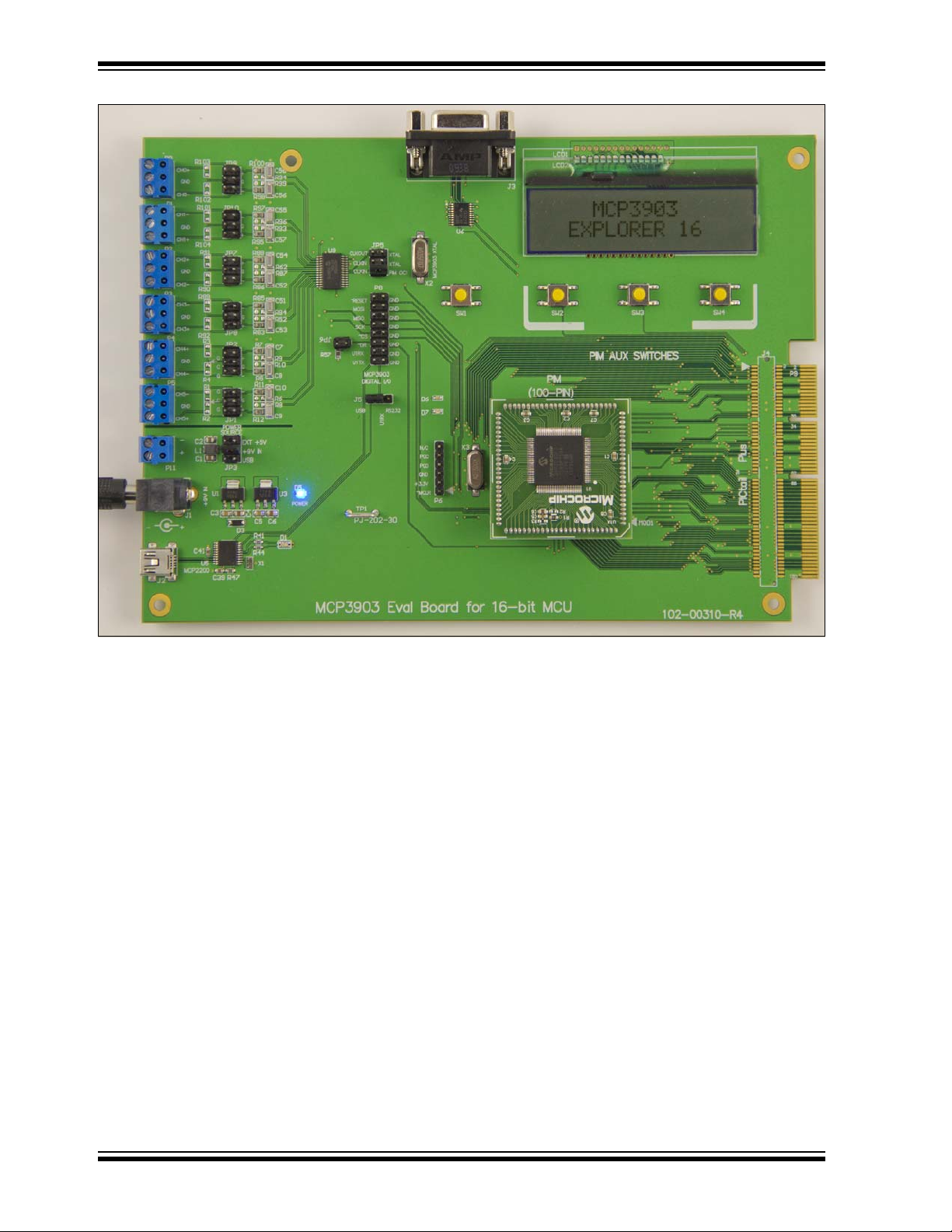
FIGURE 1-1: MCP3903 ADC Evaluation Board for 16-Bit MCUs.
DS51994A-page 6 © 2011 Microchip Technology Inc.
Page 11

Hardware Description
1.2 PIM MODULE / MCP3903 CONNECTION AND PERIPHERAL USAGE OVERVIEW
The MCP3903 ADC Evaluation Board for 16-Bit MCUs contains a 100-pin PIM socket,
compatible with Microchip’s PIM modules. The system comes with a PIM module: the
PIC24FJ128GA010.
For a complete description of the firmware programmed with these two modules, see
Chapter 1. “Hardwa re Desc ript ion ”.
RA9/10
RB8/9/10
RF2/U1RX
RF3/U1TX
OC1/RD0
IC4/RD11
IC3/RD10
INT3/RA4
SCK1/RF6
SDI1/RF7
SDO1/RF8
PIM Module
RA5
RA4
RESET
DR
CS
SCK
SDO
SDI
D6 D7
CONTROL SWITCHES (X3)
UART SERIAL TO PC COMMUNICATION
DGND DVdd
(Green)
MCP3903
SPI Serial
Interface
OSC2
Clock Generation/
Phase Correction
Six Channels
Sigma-Delta
ADC
OSC1
AVDDAGND
INT
Vref
CH0+
CH0-
CH1+
CH1-
CH2+
CH2-
CH3+
CH3-
CH4+
CH4-
CH5+
CH5-
FIGURE 1-2: Digital Connection Overview PIM/MCP3903 Connections.
Ports A, B, and D are used for signals such as push buttons, output LEDs, CS
MCLR
(for MCP3903 data mode setting). Output Capture 1 is used for MCP3903’s
and
clock generation. Serial communication is achieved through the MSSP module 1.
The MCP3903 device is an ADC with a second order modulator and a third order sync
filter . This Delt a-Sigma A/D co nverter has an adj ustable ov ersampling rat io. The CLKIN
pin of the MCP3903 is the ADC’s clock (MCLK) input. The MCP3903 ADC Evaluation
Board for 16-Bit MCUs offers two different options for the MCP3903 master clock
(MCLK).
© 2011 Microchip Technology Inc. DS51994A-page 7
Page 12

MCP3903 ADC Evaluation Board for 16-Bit MCUs User’s Guide
1.2.1 Using the Crystal X2
The MCP3903 ADC Evaluation Board for 16-Bit MCUs is populated with a 3.58 MHz
crystal, being used as a clock source, by placing jumpers in the following position on
the MCP3903 Digital I/O header block:
CLKOUT
CLKIN
CLKIN
XTAL
XTAL
PIM OC1
FIGURE 1-3: ADC Clock Selection Jumpers - External Crystal.
1.2.2 Driving the Clock with the PIM Module
The PIC® MCU can be used to generate the CLKIN (MCLK) signal for the MCP3903,
setting the ADC sample rate through the use of the output compare module OC1. To
use this, make the following jumper change to the MCP3903 Digital I/O header block:
CLKOUT
CLKIN
CLKIN
FIGURE 1-4: ADC Clock Selection Jumpers - Clock from MCU.
The signal frequency from OC1 can be changed by the user from the PC software by
changing the value in the Sampling Speed Control box from the Edit menu. A low
number will generate a high frequency signal. The value of the sampling rate, which is
directly proportional to the clock frequency from OC1, is indicated in the sampling
speed indicator box in the PC software (see Figure 2-3) for the dsPIC33 example. In
the PIC24F example, the sampling speed is constant at 4.8 ksps, regardless of the
OSR value.
XTAL
XTAL
PIM OC1
DS51994A-page 8 © 2011 Microchip Technology Inc.
Page 13

1.3 ANALOG INPUT STRUCTURE
Two differential input paths allow external signal sources to be easily connected to the
MCP3903 input. Edge connectors JP1 and JP2 are 3-pin connectors that act both as
crew-type and clip-on post connectors.
Note: To use an edge connector as a post connector, pull up the blue plastic top
to access the posts.
JP1 and JP2 can be used to force either channel from a differential to a single-ended
configuration. R3 and R4 (on CH0), and R1 and R2 (on CH2) act as locations for
burden resistor connectors for any current transformer inputs.
1.4 USB TO SERIAL CONVERTER
The MCP3903 ADC Evaluation Board for 16-Bit MCUs also contains a USB connection
for connecting the evaluation board to a PC. On the board, there is an MCP2200 USB
to UART converter that creates a virtual COM port on the PC. The MCP3903 ADC
Evaluation Board for 16-Bit MCUs also features a RS232 connector just in case it is
required. The RS232 Line driver is connected to the same UART pins of the MCU. For
this reason, a 3-pin jumper (J5) is present on the evaluation board to select which serial
communication will be used: USB or RS232. The following figure summarizes the
connections between the ADC, MCU, USB to serial converter and RS232 line driver.
Hardware Description
PIM
Module
RF6/SCK1
RF7/SDI1
RF8/SDO1
USB con
RS232
USB
MCP2200
TX
RX
RS232 Driver
RF3/U1TX
RF2/U1RX
RX
TX
FIGURE 1-5: Serial Communication Block Diagram.
MCP3903
ADC
SCK
SDO
SDI
© 2011 Microchip Technology Inc. DS51994A-page 9
Page 14

MCP3903 ADC Evaluation Board for 16-Bit MCUs User’s Guide
NOTES:
DS51994A-page 10 © 2011 Microchip Technology Inc.
Page 15

MCP3903 ADC EVALUATION BOARD
FOR 16-BIT MCUs USER’S GUIDE
Chapter 2. Code Example
2.1 DSPIC33 EXAMPLE DESCRIPTION
If the user needs to evaluate the ADC on a system that uses dsPIC33 microcontrollers,
then a PIM connector with a dsPIC33FJ256GA710A can be used on the evaluation
board.
Using this example, the user can modify all MCP3903 internal registers from the PC
software “MCP390x Data VIEW”. The UART communication speed is at 115.2 kbps.
2.1.1 SPI Communication
To transfer data from the ADC to the MCU, the SPI communication is controlled by
DMA1. DMA1 channel is set up to use nul data write to read the MCP3903 register
correctly. The DMA1 reads 7 bytes, but the first byte is not used. Before a new DMA
read takes place, the CS pin must be controlled in the software and the MCU must wait
for a new external interrupt 3 that indicates a new acquisition.
After the DMA1 transfer is finished, the DMA buffer content is moved into the Vch0 and
Vch1 buffers. The loop is repeated until Vch0 and Vch1 are filled.
Timer 8 and Timer 9 are configured to work as a 32-bit timer. This timer starts when the
acquisition is started and stopped when data buffers are full. The value indicated by this
timer will be used to evaluate the sampling speed of the ADC on the PC interface.
After the buffers are filled with the samples, the internal registers of MCP3903 are read
also using DMA1, now configured to read 16 bytes. The state of the MCP3903 internal
registers will be stored into the MCU, since later they will be sent to the PC GUI.
To set the MCP3903 configuration registers, MCU must write on the SPI bus. For this
purpose, the DMA0 channel is used and is set to do a thirteen bytes transfer from MCU
to MCP3903.
2.1.2 UART Communication
To send the acquired samples from the MCU to the PC, the UART peripheral is used.
On the board, the user can use the RS232 DB9 connector to connect to a serial port
on PC side, or it can use the USB port that creates a virtual serial port on the PC, thanks
to the MCP2200 USB to TTL converter that is connected to the MCU.
The RX pins of the MAX2323 and the MCP2200 are tightened together with the TX pin
of the UART2 from the MCU. The user needs to select from jumperJ5 if the MCU
receives data from MCP2200 or MAX2323. In firmware, the MCU is using DMA2 to do
the transfer from MCU to the PC. To receive data from the PC through UART, the RX
interrupt is used.
© 2011 Microchip Technology Inc. DS51994A-page 11
Page 16

MCP3903 ADC Evaluation Board for 16-Bit MCUs User’s Guide
Start
Initialization
Init ia lis a tion
G e t s a m ple s in to b u ffer [51 2 ]
Read Internal Registers
Wa it for P C G UI
command
Com mand
rec eiv ed
YES
C h e ck v alid ity
Command valid
YES
Write internal registers
Send samples from Buffer [512]
Send internal registers
Send FFT
(not computed here )
Update channels selection
NO
FIGURE 2-1: dsPIC33 Example Flow Chart.
2.1.3 PC Software
NO
The PC receives the data and displays it on the MCP390x Data View. The program can
display and process only two channels at the same time. To select the desired
channels, the SW4 (RD13) must be pressed.
DS51994A-page 12 © 2011 Microchip Technology Inc.
Page 17

Code Example
FIGURE 2-2: MCP3903 Data View Software - Main Screen.
Connectivity is done through the serial port. First, the user must identify the com port
number from My computer > Manage > Device Manager. After this, in “VISA resource
names”, users must find and select the correct com port number. Only after this, can
the START button be pressed to begin the data acquisition.
FIGURE 2-3: MCP3903 Data View Software - Registers and Settings Screen.
From the Edit menu, the user can open the Registers and Settings window to control
the internal registers of the MCP3903, the sampling speed of the ADC or if any
averaging should be done on the acquired samples.
From the buffer length, the user can select the amount of data that will be processed.
The maximum length is 512. From the Sampling Speed Control, the user can change
the sampling speed of the ADC. By writing a lower value, the sampling speed is
increased, and for higher values it is decreased. The accurate value of the sampling
speed is indicated in the Sampling speed indicator.
If the user wants to investigate the effect of averaging on the performance indicator, the
desired value can be written in the “Averages” control. It must be noted that the
processed buffer will decrease by a factor equal to the value of the average.
The Write Register and Read Register tabs are used to set the internal registers of
the MCP3903. With the Write Register tab they are written and with the Read
Register tab, the user can check the settings of the registers.
© 2011 Microchip Technology Inc. DS51994A-page 13
Page 18

MCP3903 ADC Evaluation Board for 16-Bit MCUs User’s Guide
The Waveform Graphs will show the signal in Time domain, while the Signal Spectrum
graphs shows the signal in Frequency domain. From the Graphs menu, under the
Signal Spectrum option, the user can find the Switch Y-axis scale option. From here,
it is possible to change the Y axis of the Signal Spectrum in linear scale or in logarithmic
scale. The spectrum signal information is obtained by performing a Fast Fourier
transformation over the Time domain signal. This Fourier transformation can be done
after the signal has been windowed. For this, the user must select the type of window
from the Window control on the lower area of the main window.
The Histogram Graph can be used to investigate the distribution of the codes. This is
especially helpful to check if a DC signal distribution is Gaussian. From the Graphs
menu, under the Histogram option, the user can Change the n umber of bits , with the
default being 40.
The indicators from the lower area of the program indicate other performance
parameters of the ADC. The main one is SINAD and related to it is Effective Number
of Bits (ENOB), used to indicate the AC signal performance. The ENOB value is
computed according to the formula below:
EQUATION 2-1:
ENOB
For DC signals, the Noise RMS signal in µV is displayed. For AC signals, the indicator
will show the RMS value of the signal.
SINAD 1.76–
----------------------------------- -=
6.02
DS51994A-page 14 © 2011 Microchip Technology Inc.
Page 19

Appendix A. Schematics and Layouts
A.1 INTRODUCTION
This appendix contains the following schematics of the MCP3903 ADC Evaluation
Board for 16-Bit MCUs.
• Schemati c - Analog
• Schemati c - LCD and UART
• Schemati c - USB and Memor y
• Schemati c - Mic roc ont roll er (MCU)
• Schemati c - PIM Modul e
• Schemati c - Pow er
• Board - Top Trace and Top Silk
• Board - Bottom Trace and Bottom Silk
• Board - Layer #2 V
• Board - Layer #3 GND
• Board - Top Silk and Pads
• Board - Bottom Silk and Pads
MCP3903 ADC EVALUATION BOARD
FOR 16-BIT MCUs USER’S GUIDE
DD
© 2011 Microchip Technology Inc. DS51994A-page 15
Page 20

MCP3903 ADC Evaluation Board for 16-Bit MCUs User’s Guide
A.2 SCHEMATIC - ANALOG
DateRevision Notes
3/31/10
F
Initial Release Build
1
REV
ADC/MPU/MEMORY
1
2
3
4
4
6
B.Popescu
of
1
F
A.Hapenciuc
Sheet
Eng:3Drawn by:
1
ADC_MPU_MEMORY.SCHDOC
M
MCP3903 Eval Board for 16-bit MCU
18PF
C37
1MR40
X2
3.579545MHZ
GNDA GNDA
C38
18PF
P1515P1313P1111P99P77P55P33P1
RF3/U1TX
GNDA
HDR2X8-O/E
10k
R57
JP6
3903_DR +3.3V
246
JP5
HDR3X2
100 R43
135
ADC CLOCK SELECT
2
1
3903_CLKIN
+3.3V
3903_RESET
3903_SDO
3903_SCK
3903_SDI
10
R59
100R69
100
100R54
GNDA
100R63
100 R68
100NF
C44
R55
25
23
26
27
24
28
SDI
SCK
SDO
DVDD
RESET
3903_CS
CS
3903_DR
100R56
16
20
21
22
17
15
18
19
DRA
DRB
DRC
OSC1
OSC2
AGND
DGND
REFIN-
P8
GNDA
P22P44P66P8
1
3903_SDO
3903_RESET
3903_SDI
8
3903_SCK
P1010P1212P1414P16
3903_CS
3903_DR
RF2/U1RX
16
Title
U9
+5V
10
R60
100NF
C45
GNDA
CH0+
AVDD1CH0-3CH1-
2
CH1+
5
4
CH3-
CH2+6CH2-7CH3+9CH4+
8
CH4-
11
10
CH5-12CH5+
MCP3903_SO28
REFIN+
14
13
GNDA
C46
100NF
3/18/10
C
Filename:
Date:
Size
68NF
68NF
C58
GNDA
DNP
R94
GNDA
GNDAGNDA
R99
DNP
C56
68NF
R100
ABC DE
1K
R98
1K
+
GNDA
246
JP9
HDR3X2
135
C
G
GNDA
DNP
R103
NET00083
NET00093
GNDA
3
2
P0C
P0B
GND
CH0+
1K
R97
-
JP10
G
GNDA
DNP
R102
NET00088
3
1
P1C
P0A
CH1-
CH0-
1
68NF
68NF
C57
68NF
C54
GNDA
GNDA
DNP
R93
R96
C55
68NF
1K
R95
-
+
GNDA
246
HDR3X2
135
GNDA
GNDA
DNP
DNP
R104
R101
GNDA
2
1
P1B
P1A
GND
CH1+
DNP
R62
GNDA
GNDA
GNDAGNDA
GNDA
R87
DNP
DNP
GNDA
C52
68NF
1K
R88
+
GNDA
246
JP7
HDR3X2
135
GNDA
DNP
R91
GNDA
2
3
P2B
P2C
GND
CH2+
1K
1K
R85
R86
-
GNDA
DNP
R90
1
P2A
CH2-
+
246
JP8
HDR3X2
135
GNDA
DNP
R89
3
P3C
CH3-
68NF
C53
DNP
R52
R84
DNP
C51
68NF
1K
R83
-
GNDA
GNDA
DNP
R92
GNDA
1
2
P3B
P3A
GND
CH3+
C7
GNDA
GNDA
DNP
R9
GNDA
GNDA
GNDAGNDA
R10
GNDA
DNP
GNDA
C8
68NF
1K
R7
+
GNDA
246
JP2
HDR3X2
135
GNDA
DNP
R3
GNDA
3
2
P4B
P4C
GND
CH4+
-
GNDA
R4
1K
R5
DNP
1
P4A3P5C
CH4-
1K
R11
+
GNDA
246
JP1
HDR3X2
135
GNDA
R1
GNDA
GND
CH5-
2
C9
GNDA
DNP
R8
GNDA
GNDAGNDA
R6
DNP
C10
68NF
1K
R12
-
GNDA
DNPR2DNP
1
P5A2P5B
CH5+
ABC DE
4
DS51994A-page 16 © 2011 Microchip Technology Inc.
Page 21

A.3 SCHEMATIC - LCD AND UART
Schematics and Layouts
D
C
Date
3/31/10
Description
Initial Design
1
Rev
4
2
B.Popescu
A.Hapenciuc
Eng:
Drawn by:
of
Sheet
6
5
Rev
5
3/18/10
Size
M
B
Date:
MCP3903 Eval Board for 16-bit MCU
Title
C D
NET00073
NET00074
NET00071
3
DB9RF
GNDA
TX
RX
1K
1K
R32
R33
U6RX
RF3/U1TX
GNDA
GNDA
U6
2
100NF
C30
+3.3V
20
19
FORCEOFF
SN75C3223PW
EN1C1+
2
RC13
C35
NET00063
100NF
100NF
C36
+3.3V
18
VCC
NET00065
100NF
GNDA
GND
17
T1OUT
NET00064
C33
RX
GNDA
14
15
13
16
R1IN
R1OUT
FORCEON
C2+5V+3C1-4C2-6V-7R2IN
8
NET00068
NET00066
100NF
NET00067
TX
T1IN
T2OUT
C34
12
9
J3
RD15/U1RTS
RC14
11
T2IN
INVALID
R2OUT
10
RD14/U1CTS
162738495
NET00075
GNDA
1
RE2/PMPD2
RE1/PMPD1
RE0/PMPD0
RE3/PMPD3
6
DB15DB04DB37DB59DB6
RE5/PMPD5
RE4/PMPD4
10
DB48DB2
RE7/PMPD7
RE6/PMPD6
11
DB7
RE0/PMPD0
7
RE2/PMPD2
RE1/PMPD1
RE3/PMPD3
RE4/PMPD4
DB411DB29DB512DB310DB18DB0
RE6/PMPD6
RE5/PMPD5
14
13
DB6
RE7/PMPD7
DB7
LCD_EXPLORER 16.SCHDOC
Filename:
B
LCD/EXPLORER 16
LCD1
LCD_2X16_BOTH
E
3
RD5/PMPRD
RD4/PMPWR
A B
1
2
VCC13RS1R/W2VEE14GND
VEE
RB15/PMPA0
NET00052
R18
NONE
+5V
GND1
15
12
GNDA
100NF
C12
R17
NONE
GNDA
+3.3V
LCD2
LCD_TM162JCAWG1
GND
VCC2RS4E6R/W5VC
1
3
+3.3V
GNDA
RD5/PMPRD
RD4/PMPWR
RB15/PMPA0
+3.3V
10K
R15
3
GNDA
R16
1.3K
VEE
A
4
© 2011 Microchip Technology Inc. DS51994A-page 17
Page 22

MCP3903 ADC Evaluation Board for 16-Bit MCUs User’s Guide
A.4 SCHEMATIC - USB AND MEMORY
4
4
6
B.Popescu
of
3
F
A.Hapenciuc
Sheet
Eng:3Drawn by:
3
GNDA
GNDA
GNDA
GNDA
GNDA GNDA
RB7/AN7/PGD
RB6/AN6/PGC
MCP3903 Eval Board for 16-bit MCU
Title
Size
M
C
dsPIC33.SCHDOC
3/18/10
Filename:
Date:
DateRevision Notes
3/31/10
1
2
3
F
1K
R37
GNDA
1K
R36
REV
Initial Schematic Design
1
dsPIC33
+3.3V
D7
RH6
RED
GM1JR35200AE
RA10/PMPA6
RA9/PMPA7
+3.3V
NONER29
47UF
C23
+
GNDA
GNDA
0.0R26
C24
100NF
VDDCORE
ENVREG
+3.3V
NONE
R25
0.0
R22
GNDA
GNDA
100
R38
D6
RH7
SML-512MW
GREEN
GNDA
100
R39
RD1
76
RD2
RD2
77
RD3/PMPBE
RD12
RD4/PMPWR
RD5/PMPRD
RD6
RD7
ENVREG
RF0
RF1
RG1
RG0
RA6
RA7
RE0/PMPD0
RE1/PMPD1
RG14
RG12
RG13
RE2/PMPD2
RE3/PMPD3
RE4/PMPD4
SS1/RD3
78
IC5/RD12
79
CN19/RD13
80
PMPWR/OC5/RD4
81
PMPRD/CN14/RD5
82
SDA2/CN15/RD6
83
SCL2/CN16/RD7
84
VCAP/VDDCORE
85
VREG
86
RF0
87
RF1
88
RG1
89
RG0
90
RA6
91
RA7
92
PMPD0/RE0
93
PMPD1/RE1
94
RG14
95
RG12
96
RG13
97
PMPD2/RE2
98
PMPD3/RE3
99
PMPD4/RE4
100
U7
18PF
C32
GNDA
X3
7.3728MHZ
GNDA
C31
18PF
3903_CLKIN
RD9
RC13
RC14
GNDA
72
73
74
70
71
69
75
VSS
RC13
RC14
IC2/RD9
OC1/RD0
IC3/RD10
IC4/RD11
RG15
T3CK/RC27T5CK/RC4
VDD
PMPD5/RE53PMPD6/RE6
PMPD7/RE75PMPA3/SDO2/CN10/RG8
6
1
2
4
+3.3V
RC2
RG15
RE6/PMPD6
RE7/PMPD7
RE5/PMPD5
RD8
1MR34
RA15/INT4
RD8
67
68
INT4/RA15
IC1/RTCC/RD8
T4CK/RC38T2CK/RC1
9
RC4
RC3
66
10
3903_DR
GNDA
64
65
VSS
INT3/RA14
PMPA4/SDI2/CN9/RG7
PMPA5/SCK2/CN8/RG6
11
12
USB_SCK
USB_SDO
RG3/SDA1
RG2/SCL1
OSC1
OSC2
+3.3V
R35
NONE
3903_RESET
3903_CS
RA2/SCL2
RA3/SDA2
+3.3V
63
56
62
61
58
59
60
57
RA2
RA3
VDD
TDI/RA4
TDO/RA5
SCL1/RG2
SDA1/RG3
OSC1/CLKI/RC12
OSC2/CLK0/RC15
dsPIC33FJ256GP710-I/PF
INT1/RE8
VSS15VDD16MCLR
RA0/TMS17INT2/RE9
C1IN+/AN5/CN7/RB5
PMPA2/SS2/CN11/RG914C1IN-/AN4/CN6/RB4
18
13
19
20
+3.3V
GNDA
USB_SS
PIC24_MCLR
RA0/TMS
RE8/INT1
RE9/INT2
RB5/AN5
USB_SDI
2.2K
2.2K
3903_SCK
3903_SDO
53
55
54
SDI1/RF7
SCK1/INT0/RF6
C2IN+/AN3/CN5/RB3
23
22
21
RB4/AN4
RB3/AN3
R28
R27
3903_SDI
SDO1/RF8
C2IN-/AN2/SS1/RB2
RB2/SS1/AN2
+3.3V
+3.3V
RF3/U1TX
RF2/U1RX
51
52
U1TX/RF3
U1RX/RF2
PGD1/AN0/RB0
PGC1/AN1/CN3/RB1
25
24
RB0/AN0
RB1/AN1
100NF
C15
+3.3V
100NF
C14
+3.3V
100NF
C16
+3.3V
100NF
C20
+3.3V
100NF
C27
+3.3V
100NF
C28
+3.3V
U2TX/RF5
50
U2RX/RF4
49
CN21/RD15
48
CN20/RD14
47
VDD
46
VSS
45
PMPA0/AN15/CN12/RB15
44
PMPA1/AN14/RB14
43
AN13/RB13
42
AN12/RB12
41
U2CTS/RF12
40
U2RTS/RF13
39
TCK/RA1
38
VDD
37
VSS
36
TDO/AN11/RB11
35
CVREF/AN10/RB10
34
C2OUT/AN9/RB9
33
C1OUT/AN8/RB8
32
AVSS
31
AVDD
30
PMPA6/RA10
29
PMPA7/RA9
28
PGD/OCFA/RB7
27
PGC2/RB6
26
100NF
C18
+3.3V
GNDA
100NF
C17
+3.3V
GNDA
100NF
C19
+3.3V
GNDA
100NF
C22
+3.3V
GNDA
100NF
C25
+3.3V
GNDA
100NF
C26
+3.3V
GNDA
RF5/PMPA8/U2TX RD1
RF4/PMPA9/U2RX
RD15/U1RTS
RD14/U1CTS
+3.3V RD13
RB15/PMPA0
GNDA
RB14/PMPA1
RB13/PMPA10
RB12/PMPA11 VDDCORE
RF12/U2CTS
RF13/U2RTS
RA1/TCK
+3.3V
RB11/PMPA12
GNDA
RB10/PMPA13
RB9/AN9
RB8/AN8
+3.3V
GNDA
RA10/PMPA6
RA9/PMPA7
PIC24_MCLR
10K
R21
+3.3V
+3.3V
GNDA
56312
4
P6
HDR6X1
PIC24 ICD
ABC DE
4
ABC DE
1
PIC24_MCLR
1KR31
+3.3V
100NF
C29
4.7K
R30
SW1
B3S-1002P
GNDA
RD7
1KR24
+3.3V
100NF
C21
4.7K
R23
GNDA
SW2
B3S-1002P
GNDA
RD6
1KR20
+3.3V
100NF
C13
4.7K
R19
GNDA
SW3
B3S-1002P
GNDA
RD13
1KR14
+3.3V
100NF
C11
4.7K
R13
GNDA
GNDA
SW4
B3S-1002P
GNDA
2
DS51994A-page 18 © 2011 Microchip Technology Inc.
Page 23

Schematics and Layouts
A.5 SCHEMATIC - MICROCONTROLLER (MCU)
4
4
6
B.Popescu
of
2
F
A.Hapenciuc
Sheet
Eng:3Drawn by:
DateRevision Notes
3/31/10
10/26/10
1
2
3
F
2
MCP2200 _ USB.SCHDOC
M
3/18/10
MCP3903 Eval Board for 16-bit MCU
C
Filename:
Date:
Size
Title
REV
Initial Schematic Design
MCP2200 communication
2
1
J2E
J2B
J2A
J2D
J2C
5
2
4
1
3
USB
DATAVIEW PORT
D-
D+
GNDA
USB_+5V
U6RX
RF2/U1RX
RF3/U1TX
HDR1X3
J5
U5-RX
ABC DE
1
MCP2200
C41
0.1uF
GNDA
D-
D+
RX
CTS
RTS
GP2
VSS
VUSB
GP0/SSPND
GP1/USBCFG
U5
VDD
470
R47
GNDA
C39
0.1uF
RESONATOR-CSTCE
MCP2200_SSOP20
GP4
GP3
GP7/TxLED
GP6/RxLED
OSC1
OSC2
TX
GP5
X1
12MHz
RST
470
R41
470
R44
GNDA
21
USB_+5V
D1
RED
4 3
GREEN
ABC DE
2
4
© 2011 Microchip Technology Inc. DS51994A-page 19
Page 24

MCP3903 ADC Evaluation Board for 16-Bit MCUs User’s Guide
A.6 SCHEMATIC - PIM MODULE
2
DateRevision Notes
1
3/31/10
F
3
4
4
6
B.Popescu
of
4
F
A.Hapenciuc
Sheet
Eng:3Drawn by:
4
PIM MODULE.SCHDOC
M
3/18/10
MCP3903 Eval Board for 16-bit MCU
C
Filename:
Date:
Size
Title
REV
Initial Schematic Design
1
RF3/U1TX
RF2/U1RX
4
26101216
P9
3
159
3903_SCK
RB2/SS1/AN2
RF3/U1TX
RF2/U1RX
4
26101216
J4
3
159
3903_SCK
RB2/SS1/AN2
RG2/SCL1
8
7
3903_SDO
RG2/SCL1
8
7
3903_SDO
RG3/SDA1
3903_SDI
RG3/SDA1
3903_SDI
GNDA
GNDA
GNDA
GNDA
RB4/AN4
RB1/AN1
14
13
11
15
RB3/AN3
RB0/AN0
RB4/AN4
RB1/AN1
14
13
11
15
RB3/AN3
RB0/AN0
+5V
+9V
+3.3V
RD15/U1RTS
RE8/INT1
18
2026303436
17
1925293335
+5V
+9V
+3.3V
RE9/INT2
GNDA
RD14/U1CTS
GNDA GNDA
+5V
+9V
+3.3V
RD15/U1RTS
RE8/INT1
18
2026303436
17
1925293335
+5V
+9V
+3.3V
RE9/INT2
GNDA
RD14/U1CTS
GNDA
GNDA
RF4/PMPA9/U2RX
RF5/PMPA8/U2TX
RA3/SDA2
RA2/SCL2
RF1
RF0
42
38
282224
404450
MEC1-160-02-L-D MATE
41
37
272123
394349
RG1
RG0
RG9/PMPA2/SS2
RG7/PMPA4/SDI2
RG6/PMPA5/SCK2
RG8/PMPA3/SDO2
GNDA
RF4/PMPA9/U2RX
RF5/PMPA8/U2TX
RA3/SDA2
RA2/SCL2
RF1
RF0
42
38
282224
404450
MEC1-160-02-L-D
41
37
272123
394349
RG1
RG0
GNDA GNDA
RG9/PMPA2/SS2
RG7/PMPA4/SDI2
RG6/PMPA5/SCK2
RG8/PMPA3/SDO2
RB9/AN9
RB8/AN8
RB9/AN9
RB8/AN8
RA10/PMPA6
GNDA
RA9/PMPA7
GNDA
RA10/PMPA6
GNDA
RA9/PMPA7
3903_DR
RA15/INT4
3903_DR
RA15/INT4
RF13/U2RTS
524648
54
514547
53
RF12/U2CTS
RF13/U2RTS
524648
54
514547
53
RF12/U2CTS
+5V
+3.3V
56
586068
55
575967
+5V
+3.3V
+5V
+3.3V
56
586068
55
575967
+5V
+3.3V
+9V
RG1
RG0
66
62
65
61
+9V
+9V
RG1
RG0
66
62
65
61
+9V
RG13
RG15
RG13
RG15
RG14
RG12
RG14
RG12
RA1/TCK
RA0/TMS
RA1/TCK
RA0/TMS
3903_RESET
RA7
74
73
RA6
3903_CS
3903_RESET
RA7
74
73
RA6
3903_CS
RB13/PMPA10
RB11/PMPA12
PIC24_MCLR
RB7/AN7/PGD
80
767072
8478828892
79
756971
7781838791
RB5/AN5
RB6/AN6/PGC
RB12/PMPA11
RB10/PMPA13
RB13/PMPA10
RB11/PMPA12
PIC24_MCLR
RB7/AN7/PGD
80
767072
8478828892
79
756971
7781838791
RB5/AN5
RB6/AN6/PGC
RB12/PMPA11
RB10/PMPA13
RB15/PMPA0
RC2
86
85
RB14/PMPA1
RB15/PMPA0
RC2
86
85
RB14/PMPA1
RD3/PMPBE
RD5/PMPRD
RD9
RD7
RD1
RC14
RC4
104
1009496
90
98
102
999395
89
97
103
101
RD8
RD6
RD2
RC3
RC13
3903_CLKIN
RD4/PMPWR
RD3/PMPBE
RD5/PMPRD
RD9
RD7
RD1
RC14
RC4
104
1009496
90
98
102
999395
89
97
103
101
RD8
RD6
RD2
RC3
RC13
3903_CLKIN
RD4/PMPWR
GNDA
+3.3V
RE7/PMPD7
RE5/PMPD5
RE3/PMPD3
RE1/PMPD1
RD13
118
120
106
108
117
119
113 114
109 110
115 116
107
105
111 112
RD12
+3.3V
GNDA
RE6/PMPD6
RE4/PMPD4
RE2/PMPD2
RE0/PMPD0
GNDA
+3.3V
RE7/PMPD7
RE5/PMPD5
RE3/PMPD3
RE1/PMPD1
RD13
118
120
106
108
117
119
113 114
109 110
115 116
107
105
111 112
RD12
+3.3V
GNDA
RE6/PMPD6
RE4/PMPD4
RE2/PMPD2
RE0/PMPD0
PIM MODLUE
ABC DE
RD3/PMPBE
RD12
RD4/PMPWR
RD5/PMPRD
RD6
RD7
ENVREG
RF0
RF1
RG1
RG0
RA6
RA7
RE0/PMPD0
RE1/PMPD1
RG14
RG12
RG13
RE3/PMPD3
RE4/PMPD4
3903_CLKIN
RD9
RC14
RC13
GNDA
72
70
71
69
73
74
75
VSS
RC13
RC14
IC2/RD9
OC1/RD0
IC3/RD10
IC4/RD11
RD1
76
RD2
77
SS1/RD3
78
IC5/RD12
79
CN19/RD13
80
PMPWR/OC5/RD4
81
PMPRD/CN14/RD5
82
SDA2/CN15/RD6
83
SCL2/CN16/RD7
84
VCAP/VDDCORE
85
VREG
86
RF0
87
RF1
88
RG1
89
RG0
90
RA6
91
RA7
92
PMPD0/RE0
93
PMPD1/RE1
94
RG14
95
RG12
96
RG13
97
PMPD2/RE2
98
PMPD3/RE3
99
PMPD4/RE4
100
MOD1
PIM 100-PIN
RG15
T3CK/RC27T5CK/RC4
VDD
PMPD5/RE53PMPD6/RE6
PMPD7/RE75PMPA3/SDO2/CN10/RG8
6
1
2
4
+3.3V
RC2
RG15
RE7/PMPD7
RE6/PMPD6
RE5/PMPD5
RA15/INT4
RD8
68
67
INT4/RA15
IC1/RTCC/RD8
T4CK/RC38T2CK/RC1
9
RC4
RC3
3903_DR
GNDA
66
65
VSS
INT3/RA14
PMPA4/SDI2/CN9/RG7
PMPA5/SCK2/CN8/RG6
11
10
USB_SCK
USB_SDO
3903_RESET
3903_CS
RG2/SCL1
RA2/SCL2
RA3/SDA2
OSC1
OSC2
+3.3V
62
61
60
64
58
57
59
63
RA2
RA3
VDD
TDI/RA4
TDO/RA5
SCL1/RG2
OSC1/CLKI/RC12
OSC2/CLK0/RC15
INT1/RE8
VSS15VDD16MCLR
RA0/TMS17INT2/RE9
PMPA2/SS2/CN11/RG914C1IN-/AN4/CN6/RB4
18
13
19
12
+3.3V
GNDA
RA0/TMS
RE9/INT2
RE8/INT1
PIC24_MCLR
USB_SS
USB_SDI
3903_SCK
3903_SDO
RG3/SDA1
54
56
55
SDI1/RF7
SDA1/RG3
SCK1/INT0/RF6
C2IN+/AN3/CN5/RB3
C1IN+/AN5/CN7/RB5
22
20
21
RB4/AN4
RB3/AN3
RB5/AN5
3903_SDI
RF3/U1TX
RF2/U1RX
53
52
51
U1TX/RF3
U1RX/RF2
SDO1/RF8
PGD1/AN0/RB0
C2IN-/AN2/SS1/RB2
PGC1/AN1/CN3/RB1
25
23
24
RB0/AN0
RB1/AN1
RB2/SS1/AN2
U2TX/RF5
50
U2RX/RF4
49
CN21/RD15
48
CN20/RD14
47
VDD
46
VSS
45
PMPA0/AN15/CN12/RB15
44
PMPA1/AN14/RB14
43
AN13/RB13
42
AN12/RB12
41
U2CTS/RF12
40
U2RTS/RF13
39
TCK/RA1
38
VDD
37
VSS
36
TDO/AN11/RB11
35
CVREF/AN10/RB10
34
C2OUT/AN9/RB9
33
C1OUT/AN8/RB8
32
AVSS
31
AVDD
30
PMPA6/RA10
29
PMPA7/RA9
28
PGD/OCFA/RB7
27
PGC2/RB6
26
RF5/PMPA8/U2TX RD1
RF4/PMPA9/U2RX RD2
RD15/U1RTS
RD14/U1CTS
+3.3V RD13
RB15/PMPA0
RB14/PMPA1
RB13/PMPA10
RB12/PMPA11 VDDCORE
RF12/U2CTS
RF13/U2RTS
RA1/TCK
+3.3V
RB11/PMPA12
GNDA
RB10/PMPA13
RB9/AN9
RB8/AN8
+3.3V
GNDA GNDA
RA10/PMPA6
RA9/PMPA7 RE2/PMPD2
RB7/AN7/PGD
RB6/AN6/PGC
ABC DE
1
2
4
DS51994A-page 20 © 2011 Microchip Technology Inc.
Page 25

A.7 SCHEMATIC - POWER
Schematics and Layouts
D
C
Date
3/31/10
Description
Initial Design
1
Rev
3
GNDA
GNDA
EXT +5V
+9V IN
135
JP3
HDR3X2
246
GNDA GNDA
GNDA
2
GNDAGNDA
TP1
GND
PJ-202-30
+3.3V
100
R58
+3.3V
100NF
C5
2
OUT
GND
1
U3
LM1117-3.3
IN
3
4.7UF
C6
D5
L1
BLUE
GM1B55250AC
+5V
10UH
GNDA
POWER
10UF
C1
4.7UF
C2
USB
1
4
4
B.Popescu
A.Hapenciuc
Eng:
Drawn by:
of
Sheet
6
6
Rev
6
3/18/10
Size
M
B
Date:
MCP3903 Eval Board for 16-bit MCU
Title
C D
POWER
USB_+5V
GNDA
C3
100NF
2
OUT
GND
1
U1
LM1117-5.0
+9V
POWER
+9V IN
GNDA
IN
3
10UF
C4
GNDA
D3
A K
MBR0520LT1
GNDA
321
J1
RAPC722
GNDA
EXT_+5V
2
1
P11B
P11A
POWER
EXT +5V
A B
1
2
3
4
POWER.SCHDOC
Filename:
B
A
© 2011 Microchip Technology Inc. DS51994A-page 21
Page 26

MCP3903 ADC Evaluation Board for 16-Bit MCUs User’s Guide
A.8 BOARD - TOP TRACE AND TOP SILK
A.9 BOARD - BOTTOM TRACE AND BOTTOM SILK
DS51994A-page 22 © 2011 Microchip Technology Inc.
Page 27

A.10 BOARD - LAYER #2 VDD
Schematics and Layouts
A.11 BOARD - LAYER #3 GND
© 2011 Microchip Technology Inc. DS51994A-page 23
Page 28

MCP3903 ADC Evaluation Board for 16-Bit MCUs User’s Guide
A.12 BOARD - TOP SILK AND PADS
A.13 BOARD - BOTTOM SILK AND PADS
DS51994A-page 24 © 2011 Microchip Technology Inc.
Page 29

MCP3903 ADC EVALUATION BOARD
FOR 16-BIT MCUs USER’S GUIDE
Appendix B. Bill of Materials (BOM)
TABLE B-1: BILL OF MATERIALS (BOM)
Qty Reference Description Manufacturer Part Number
2 C1,C4 CAP CER 10UF 16V Y5V 0805 TDK Corp. C2012Y5V1C106Z
25 C11<>C22
C24<>C30
C33,C34,C35
C36,C39,C41
2 C2,C6 CAP CER 4.7UF 25V Y5V 0805 TDK Corp. C2012Y5V1E475Z
1 C23 CAPACITOR TANT 47UF 6.3V 20% SMD Kemet
5 C3,C5,C44
C45,C46
4 C31,C32
C37,C38
12 C7,C8,C9, C10
C51<>C58
1 D1 LED 2X1.2MM RD/GN WTR CLR SMD Kingbright Corp. APHBM2012SURKCGKC
1 D3 DIODE SCHOTTKY 20V 0.5A SOD123 ON Semi. MBR0520LT1G
1 D5 LED BLUE 470NM CLEAR LENS (0603
1 D6 LED 570NM GRN WHT/DIFF 0603 SMD Rohm Semi. SML-512MWT86
1 D7 LED RED 470NM CLEAR LENS (0603
4 Ea. Conner of
PCB
4 Ea. Conner of
PCB
1 J1 CONN POWERJACK MINI .08" R/A T/H Switchcraft
1 J2 Mini USB Type B Surface Mount Samtec MUSB-05-S-B-SM-A
1 J3 C ONN D-S UB RCP T R/A 9POS 15GO LD Tyco Electroni cs 1734354-2
1 J4 "DO NOT INSTALL"
1 J5 3 x 1 Header 2.54mm - 8 JP1,JP2,JP3
JP5,JP7,JP8
JP9,JP10
1 JP6 2 x 1 Header 2.54mm - 9 Jumper Shunts CONN JUMPER SHORTING TIN Sullins Connector
Note 1: The component s l isted in t his Bi ll of Mate rials are re presen tat ive o f the PCB a ssembl y. The released BOM
used in manufacturing uses all RoHS-compliant components.
CAP CER .10UF 25V X7R 10% 0603 TDK Corp. C1608X7R1E104K
®
CAP CER .10UF 25V X7R 10% 0805 TDK Corp. C2012X7R1E104K
CAP CER 18PF 50V C0G 5% 0603 TDK Corp. C1608C0G1H180J
CAP CER 68000PF 25V C0G 5% 1206 TDK Corp. C3216C0G1E683J
Para Light Corp. L-C191LBCT-U1
Blue)
Para Light Corp. L-C192KRCT-U1
Red)
STANDOFF HEX .500/4-40THR NYLON Keystone 1902C
SCREW MACH PHIL 4-40X3/8 NYLON Building Fasteners NY PMS 440 0038 PH
®
Samtec MEC1-160-02-L-D-A
120-pin MINI EDGE CARD SOCKET
3 X 2 Header 2.54mm on center 6
mm/2.5mm
Samtec TSW-103-07-G-D
Solutions
T491A476M006AT
RAPC722X
STC02SYAN
© 2011 Microchip Technology Inc. DS51994A-page 25
Page 30

Bill of Materials (BOM)
TABLE B-1: BILL OF MATERIALS (BOM) (CONTINUED)
Qty Reference Description Manufacturer Part Number
1 L1 Shielded 10uH Power Inductor 0805 Coilcraf t 0805PS-103KLC
1 LCD1 "DO NOT INSTALL" - 1 LCD2 16X2 FTN Reflective No. BLWT COG 3V Tianma TM162JCAWG1
4 MOD1 25 X 1 Header 1.27mm on center Samtec MTMS-125-01-G-S-230
6 P0,P1,P2,P3
P4,P5
1 P0,P1,P2,P3
P4,P5,P11
1 P11 CONN TERM BLK PLUG 6A 3.5MM 2POS Keystone 8722
1 P6 6 x 1 Header 2.54mm - 1 P8 8 X 2 CONN HEADER 8POS .100" DUAL
1 P9 "DO NOT INSTALL” - 1 PCB RoHS Compliant Bare PCB, MCP3901
24 R1,R2,R3,R4
R6,R8,R9
R10,R16,
R52,R62
R84,R87
R89<>R94
R96,R99
R101<>R104
4 R13,R19
R23,R30
8 R14,R20, R24,
R31 R32,R33
R36, R37
3 R21,R57 RES 10.0K OHM 1/10W 1% 0603 SMD Rohm Semi. MCR03EZPFX1002
5 R17,R18,R25
R29,R35
2 R15,R22,R26 RES 0.0 OHM 1/10W 5% 0603 SMD Rohm Semi. MCR03EZPJ000
2 R27,R28 RES 2.20K OHM 1/10W 1% 0603 SMD Rohm Semi. MCR03EZPFX2201
2 R34,R40 RES 1.00M OHM 1/10W 1% 0603 SMD Rohm Semi. MCR03EZPFX1004
10 R38,R39,R43,R
54,R55,R56,R5
8 R63,R68,R69
3 R41,R44,R47 RES 470 OHM 1/10W 5% 0603 SMD Panasonic ERJ-3GEYJ471V
7 R44,R70,R71,
R72,R74,R75
R76
Note 1: The component s l isted in t his Bi ll of Mate rials are re presen tat ive o f the PCB a ssembl y. The released BOM
used in manufacturing uses all RoHS-compliant components.
CONN TERM BLK PLUG 6A 3.5MM 3POS Keystone 8723
TERM BLK PIN HEADER 24Pin Pos One
24 Pin Header for 1 Board (20 pins
needed)
TIN
Eval. Board for 16-bit MCU
(0805) "DO NOT INSTALL" - -
RES 4.70K OHM 1/10W 1% 0603 SMD Rohm Semi. MCR03EZPFX4701
RES 1.00K OHM 1/10W 1% 0603 SMD Rohm Semi. MCR03EZPFX1001
(0603) "DO NOT INSTALL" - -
RES 100 OHM 1/10W 1% 0603 SMD Rohm Semi. MCR03EZPFX1000
RES 100K OHM 1/10W 1% 0603 SMD Rohm Semi. MCR03EZPFX1003
Keystone 8724
Samtec TSW-104-17-T-D
- 104-00221
© 2011 Microchip Technology Inc. DS51994A-page 26
Page 31

Bill of Materials (BOM)
TABLE B-1: BILL OF MATERIALS (BOM) (CONTINUED)
Qty Reference Description Manufacturer Part Number
12 R5,R7,R11
R12,R83,R85
R86,R88,R95
R97,R98 R100
2 R59,R60 RES 10.0 OHM 1/8W 1% 0805 SMD Rohm Semi. MCR10EZHF10R0
4 SW1,SW2
SW3,SW4
1 TP1 Wire Test Point 0.3" Length Components Corp. PJ-202-30
1 U1 IC REG LDO 800MA 5.0V SOT-223 National Semi. LM1117MP-5.0/NOPB
1 U3 IC REG LDO 800MA 3.3V SOT-223 National Semi. LM1117MP-3.3/NOPB
1 U6 IC DRVR/RCVR MLTCH RS232 20TSSOP Texas Instruments SN75C3223PWR
1 U7 "DO NOT INSTALL" - 1 U9 IC ENERGY METER 28SSOP Microchip MCP3903
1 X2 CRYSTAL 3.579545MHZ 18PFFUND
Note 1: The component s l isted in t his Bi ll of Mate rials are re presen tat ive o f the PCB a ssembl y. The released BOM
used in manufacturing uses all RoHS-compliant components.
RES 1.0K OHM .1% 1/4W 0805 SMD Susumu Co., LTD. RGH2012-2E-P-102-B
SWITCH TACT 6MM 230GF H=4.3MM Omron Electronic
Components ECB Division
Abracon Corp. ABLS-3.579545MHZ-B2-T
SMD
B3S-1002P
© 2011 Microchip Technology Inc. DS51994A-page 27
Page 32

Worldwide Sales and Service
AMERICAS
Corporate Office
2355 West Chandler Blvd.
Chandler, AZ 85224-6199
Tel: 480-792-7200
Fax: 480-792-7277
Technical Support:
http://www.microchip.com/
support
Web Address:
www.microchip.com
Atlanta
Duluth, GA
Tel: 678-957-9614
Fax: 678-957-1455
Boston
Westborough, MA
Tel: 774-760-0087
Fax: 774-760-0088
Chicago
Itasca, IL
Tel: 630-285-0071
Fax: 630-285-0075
Cleveland
Independence, OH
Tel: 216-447-0464
Fax: 216-447-0643
Dallas
Addison, TX
Tel: 972-818-7423
Fax: 972-818-2924
Detroit
Farmington Hills, MI
Tel: 248-538-2250
Fax: 248-538-2260
Indianapolis
Noblesville, IN
Tel: 317-773-8323
Fax: 317-773-5453
Los Angeles
Mission Viejo, CA
Tel: 949-462-9523
Fax: 949-462-9608
Santa Clara
Santa Clara, CA
Tel: 408-961-6444
Fax: 408-961-6445
Toronto
Mississauga, Ontario,
Canada
Tel: 905-673-0699
Fax: 905-673-6509
ASIA/PACIFIC
Asia Pacific Office
Suites 3707-14, 37th Floor
Tower 6, The Gateway
Harbour City, Kowloon
Hong Kong
Tel: 852-2401-1200
Fax: 852-2401-3431
Australia - Sydney
Tel: 61-2-9868-6733
Fax: 61-2-9868-6755
China - Beijing
Tel: 86-10-8569-7000
Fax: 86-10-8528-2104
China - Chengdu
Tel: 86-28-8665-5511
Fax: 86-28-8665-7889
China - Chongqing
Tel: 86-23-8980-9588
Fax: 86-23-8980-9500
China - Hangzhou
Tel: 86-571-2819-3180
Fax: 86-571-2819-3189
China - Hong Kong SAR
Tel: 852-2401-1200
Fax: 852-2401-3431
China - Nanjing
Tel: 86-25-8473-2460
Fax: 86-25-8473-2470
China - Qingdao
Tel: 86-532-8502-7355
Fax: 86-532-8502-7205
China - Shanghai
Tel: 86-21-5407-5533
Fax: 86-21-5407-5066
China - Shenyang
Tel: 86-24-2334-2829
Fax: 86-24-2334-2393
China - Shenzhen
Tel: 86-755-8203-2660
Fax: 86-755-8203-1760
China - Wuhan
Tel: 86-27-5980-5300
Fax: 86-27-5980-5118
China - Xian
Tel: 86-29-8833-7252
Fax: 86-29-8833-7256
China - Xiamen
Tel: 86-592-2388138
Fax: 86-592-2388130
China - Zhuhai
Tel: 86-756-3210040
Fax: 86-756-3210049
ASIA/PACIFIC
India - Bangalore
Tel: 91-80-3090-4444
Fax: 91-80-3090-4123
India - New Delhi
Tel: 91-11-4160-8631
Fax: 91-11-4160-8632
India - Pune
Tel: 91-20-2566-1512
Fax: 91-20-2566-1513
Japan - Yokohama
Tel: 81-45-471- 6166
Fax: 81-45-471-6122
Korea - Daegu
Tel: 82-53-744-4301
Fax: 82-53-744-4302
Korea - Seoul
Tel: 82-2-554-7200
Fax: 82-2-558-5932 or
82-2-558-5934
Malaysia - Kuala Lumpur
Tel: 60-3-6201-9857
Fax: 60-3-6201-9859
Malaysia - Penang
Tel: 60-4-227-8870
Fax: 60-4-227-4068
Philippines - Manila
Tel: 63-2-634-9065
Fax: 63-2-634-9069
Singapore
Tel: 65-6334-8870
Fax: 65-6334-8850
Tai wan - Hsin Chu
Tel: 886-3-6578-300
Fax: 886-3-6578-370
Taiwan - Kaohsiung
Tel: 886-7-213-7830
Fax: 886-7-330-9305
Taiwan - Taipei
Tel: 886-2-2500-6610
Fax: 886-2-2508-0102
Thailand - Bangkok
Tel: 66-2-694-1351
Fax: 66-2-694-1350
EUROPE
Austria - Wels
Tel: 43-7242-2244-39
Fax: 43-7242-2244-393
Denmark - Copenhagen
Tel: 45-4450-2828
Fax: 45-4485-2829
France - Paris
Tel: 33-1-69-53-63-20
Fax: 33-1-69-30-90-79
Germany - Munich
Tel: 49-89-627-144-0
Fax: 49-89-627-144-44
Italy - Milan
Tel: 39-0331-742611
Fax: 39-0331-466781
Netherlands - Drunen
Tel: 31-416-690399
Fax: 31-416-690340
Spain - Madrid
Tel: 34-91-708-08-90
Fax: 34-91-708-08-91
UK - Wokingham
Tel: 44-118-921-5869
Fax: 44-118-921-5820
05/02/11
DS51994A-page 28 © 2011 Microchip Technology Inc.
 Loading...