

Page 1

MCP3901 and PIC18F65J90
Energy Meter Reference Design
User’s Guide
© 2012 Microchip Technology Inc. DS51968A
Page 2

Note the following details of the code protection feature on Microchip devices:
• Microchip products meet the specification contained in their particular Microchip Data Sheet.
• Microchip believes that its family of products is one of the most secure families of its kind on the market today, when used in the
intended manner and under normal conditions.
• There are dishonest and possibly illegal methods used to breach the code protection feature. All of these methods, to our
knowledge, require using the Microchip products in a manner outside the operating specifications contained in Microchip’s Data
Sheets. Most likely, the person doing so is engaged in theft of intellectual property.
• Microchip is willing to work with the customer who is concerned about the integrity of their code.
• Neither Microchip nor any other semiconductor manufacturer can guarantee the security of their code. Code protection does not
mean that we are guaranteeing the product as “unbreakable.”
Code protection is constantly evolving. We at Microchip are committed to continuously improving the code protection features of our
products. Attempts to break Microchip’s code protection feature may be a violation of the Digital Millennium Copyright Act. If such acts
allow unauthorized access to your software or other copyrighted work, you may have a right to sue for relief under that Act.
Information contained in this publication regarding device
applications and t he lik e is provided only for your convenience
and may be su perseded by upda t es . It is y our responsibility to
ensure that your application meets with your specifications.
MICROCHIP MAKES NO REPRESENTATIONS OR
WARRANTIES OF ANY KIND WHETHER EXPRESS OR
IMPLIED, WRITTEN OR ORAL, STATUTORY OR
OTHERWISE, RELATED TO THE INFORMATION,
INCLUDING BUT NOT LIMITED TO ITS CONDITION,
QUALITY, PERFORMANCE, MERCHANTABILITY OR
FITNESS FOR PURPOSE. Microchip disclaims all liability
arising from this information and its use. Use of Microchip
devices in life supp ort and/or safety ap plications is entir ely at
the buyer’s risk, and the buyer agrees to defend, indemnify and
hold harmless M icrochip from any and all dama ges, claims,
suits, or expenses re sulting from such use. No licens es are
conveyed, implicitly or otherwise, under any Microchip
intellectual property rights.
Trademarks
The Microchip name and logo, the Microchip logo, dsPIC,
K
EELOQ, KEELOQ logo, MPLAB, PIC, PICmicro, PICSTART,
32
PIC
logo, rfPIC and UNI/O are registered trademarks of
Microchip Technology Incorporated in the U.S.A. and other
countries.
FilterLab, Hampshire, HI-TECH C, Linear Active Thermistor,
MXDEV, MXLAB, SEEVAL and The Embedded Control
Solutions Company are registered trademarks of Microchip
Technology Incorporated in the U.S.A.
Analog-for-the-Digital Age, Application Maestro, chipKIT,
chipKIT logo, CodeGuard, dsPICDEM, dsPICDEM.net,
dsPICworks, dsSPEAK, ECAN, ECONOMONITOR,
FanSense, HI-TIDE, In-Circuit Serial Programming, ICSP,
Mindi, MiWi, MPASM, MPLAB Certified logo, MPLIB,
MPLINK, mTouch, Omniscient Code Generation, PICC,
PICC-18, PICDEM, PICDEM.net, PICkit, PICtail, REAL ICE,
rfLAB, Select Mode, Total Endurance, TSHARC,
UniWinDriver, WiperLock and ZENA are trademarks of
Microchip Technology Incorporated in the U.S.A. and other
countries.
SQTP is a service mark of Microchip Technology Incorporated
in the U.S.A.
All other trademarks mentioned herein are property of their
respective companies.
© 2012, Microchip Technology Incorporated, Printed in the
U.S.A., All Rights Reserved.
Printed on recycled paper.
ISBN: 978-1-61341-960-1
Microchip received ISO/TS-16949:2009 certification for its worldwide
headquarters, design and wafer fabrication facilities in Chandler and
Tempe, Arizona; Gresham, Oregon and design centers in California
and India. The Company’s quality system processes and procedures
are for its PIC
devices, Serial EEPROMs, microperipherals, nonvolatile memory and
analog products. In addition, Microchip’s quality system for the design
and manufacture of development systems is ISO 9001:2000 certified.
®
MCUs and dsPIC® DSCs, KEELOQ
®
code hopping
DS51968A-page 2 © 2012 Microchip Technology Inc.
Page 3

MCP3901 AND PIC18F65J90
ENERGY METER
REFERENCE DESIGN
Table of Contents
Preface ...........................................................................................................................7
Introduction............................................................................................................7
Document Layout .................................................................................................. 8
Conventions Used in this Guide............................................................................ 9
Recommended Reading.............................................................. .. ......................10
The Microchip Web Site...................................................................................... 10
Customer Support.................... .................................... .................. .....................10
Document Revision History................................................................................. 10
Chapter 1. Product Overview
1.1 Introduction ...................................................................................................11
1.2 What the MCP3901 and PIC18F65J90 Energy Meter
Reference Design Kit Includes ............................................................... 12
1.3 Getting Sta rted .... .................................................................................. ....... 12
Chapter 2. Hardware
2.1 Overview ............. ......................................................................................... 13
2.2 Input and Analog Front End .........................................................................16
Chapter 3. Calculation Engine and Register Description
3.1 Calculati on E n g in e Si g nal Flow Summary ................................................... 17
3.2 Register L is t ................................................................................................. 18
3.3 MODE .......................................................................................................... . 19
3.4 STATUS .......... .. ........................................................................................... 20
3.5 CAL_CONT R O L ........................................................................................... 20
3.6 LINE_CYC ................. .. ................................................................................ 21
3.7 LINE_CYC _ C N T ............. ... ..................................................... .. .. ................ 2 1
3.8 RAW2_I_RMS ..............................................................................................21
3.9 RAW_I_RM S .................... .......................................... .................................. 22
3.10 I_RMS ............... ......................................................................................... 22
3.11 RAW2_V _ R M S ......................................................................................... 22
3.12 RAW_V_ R M S .......................... ........................................................ ......... 22
3.13 V_RMS ....... ... .. ........................................................................................... 22
3.14 LINE_F R E Q UE N CY ............................................... .................................... 23
3.15 RAW_PO WER_ACT ......................................... ........................................ 23
3.16 POWER_ A CT ..................................... .......................................... .............. 23
3.17 POWER_APP ............................................................................................23
3.18 RAW_PO WER_REACT .......... ................ ................................................... 24
3.19 POWER_ R EA CT ...... .. .. ............................. .......................................... ....... 24
© 2012 Microchip Technology Inc. DS51968A-page 3
Page 4

MCP3901 and PIC18F65J90 Energy Meter Reference De sign
3.20 PERIOD .... ....................................................... ........................................... 24
3.21 ENERG Y _ AC T ............. .. ............................ ................................................ 24
3.22 ENERGY_APP ..........................................................................................25
3.23 I_ABS_MAX ...............................................................................................25
3.24 V_ABS _ M A X ............. ... .............................................................................. 2 5
3.25 ENERG Y _ RE A C T ...................................................................................... 25
3.26 PHASE_COMPENSATION ........................................................................ 25
3.27 OFFSE T _ I_ R M S .. .. .................................................................................. . 26
3.28 OFFS ET _ V _RMS . .. ..................................................... .. ... ......................... 2 6
3.29 GAIN_I_RMS ............................................................................................. 26
3.30 GAIN_V _ R MS ............................................................................................ 26
3.31 OFFSE T _ P O WE R _ A CT .................... ...................................................... 26
3.32 GAIN_P O WER_ACT ........ .. ........................................................................ 27
3.33 OFFSE T _ P O WE R _ RE ACT .............. ........................................................ 27
3.34 GAIN_P O WER_REACT ... .................................................................... ...... 27
3.35 GAIN_E N E RGY_ACT ................................................................................ 27
3.36 GAIN_ENERGY_APP ................................................................................ 27
3.37 GAIN_E N E RGY_REACT . .. .. ...................................................................... 27
3.38 CF_PU LSE_WIDTH ............. ...................................................................... 28
3.39 GAIN_D E N R_ENERGY_A C T ......... ................ ........................................... 28
3.40 GAIN_N U MR_ENERGY_ A CT ............................................ ....................... 28
3.41 MODE1 _ D EF ............................................................. .............................. 28
3.42 CAL_ST A T US ........... ... .......................... .. .. ................................................ 28
3.43 MAXIMUM CURRENT ............................................................................. 29
3.44 CALIB R AT ION_VOLTAG E ....... .. ..................................................... .. ... ... 29
3.45 CALIBRATION_CURRENT ......................................................................29
3.46 CALIB R AT ION_FREQUE N CY . ................................................................. 29
3.47 METER _ C ON S T A N T ......................................... ....................................... 2 9
3.48 CALIB R A T I O N _ L INE _ C Y CLE ................................................. ... .. ............ 30
3.49 GAIN_D E N R_ENERGY_R EA C T ............ .. ... ............................................. 30
3.50 GAIN_N U MR_ENERGY_ R E ACT ............. ................................................ 30
3.51 PHASE_COMPENSATION_90 ................................................................. 30
3.52 CREEP_THRSHOLD_MINUTE ................................................................. 30
3.53 CREEP_THRSHOLD_SECOND ................................................................30
Chapter 4. Meter Protocol and Timings
4.1 Protocol ..................................................... .. ... ............................................. 31
Appendix A. Schematic and Layouts
A.1 Introduction .................................................................................................. 33
A.2 Schematics and PCB Layout ........................ ......................... .. .. ..................33
A.3 Board – ADC Schematic ............................................................................. 34
A.4 Board – MCU S c he matic ........... .. ............. .. ... ............................................. 35
A.5 Board – LCD and USB Schematic .............. .. ............................... ................36
A.6 Board – Top Silk and Pads ........................ .. ..................... .......................... 37
A.7 Board – Top Copper .................................................................................... 38
DS51968A-page 4 © 2012 Microchip Technology Inc.
Page 5

A.8 Board – Bottom Copper ...............................................................................39
A.9 Board – Bottom Silk and Pads ..................... .. .. .. ............................. .. ...........40
A.10 Board – To p 3 D ............................................................. .. .. ............. ... .. ....... 41
A.11 Board – Bo tt om 3D ...... ............. ... .. ............. .. .. ........................... .. .. ............ 42
Appendix B. Bill of Materials (BOM)
Worldwide Sales and Service ....................................................................................46
© 2012 Microchip Technology Inc. DS51968A-page 5
Page 6

MCP3901 and PIC18F65J90 Energy Meter Reference De sign
DS51968A-page 6 © 2012 Microchip Technology Inc.
Page 7

MCP3901 AND PIC18F65J90
ENERGY METER
REFERENCE DESIGN
Preface
NOTICE TO CUSTOMERS
All documentation becomes dated, and this manual is no exception. Microchip tools and
documentation are constantly evolving to meet customer needs, so some actual dialogs
and/or tool descriptions may differ from those in this document. Please refer to our web site
(www.microchip.com) to obtain the latest documentation available.
Documents are identified with a “DS” number. This number is located on the bottom of each
page, in front of the p age number. The numbering convention for the DS number is
“DSXXXXXA”, where “XXXXX” is the document number and “A” is the revision level of the
document.
For the most up-to-date information on development tools, see the MPLAB
Select the Help menu, and then Topics to open a list of available online help files.
®
IDE online help.
INTRODUCTION
This chapter contains general information that will be useful to know before using the
MCP3901 and PIC18F65J90 Energy Meter Reference Design User’s Guide. Items
discussed in this chapter include:
• Document Layout
• Conventions Used in this Guide
• Recommended Reading
• The Microchip Web Site
• Customer Support
• Document Revision History
© 2012 Microchip Technology Inc. DS51968A-page 7
Page 8

MCP3901 and PIC18F65J90 Energy Meter Reference De sign
DOCUMENT LAYOUT
This document describes how to use the MCP3901 and PIC18F65J90 Energy Meter
Reference Design as a development tool to emulate and debug firmware on a target
board. The manual layout is as follows:
• Chapter 1. “Product Overview” – Important information on using the MCP3901
and PIC18F65J90 Energy Meter Reference Design including a Getting Started
section that describes wiring the line and load connections.
• Chapter 2. “Hardwa re ” – Includes details on the function blocks of the meter
including the analog front end design, phase lock loop circuitry, and power supply
design.
• Chapter 3. “Calculation Engine and Register Description” – This section
describes the digital signal flow for all power output quantities such as RMS
current, RMS voltage, active power, and apparent power. This section also
includes the calibration register’s detail.
• Chapter 4. “Meter Protocol and Timings”– This chapter describes the protocol
used for accessing the registers, including commands that are used to interface to
the meter.
• Appendix A. “Schematic and Layouts” – Shows the schematic and layout
diagrams.
• Appendix B. “Bill of Materials (BOM)” – Lists the parts used to build the
MCP3901 and PIC18F65J90 Energy Meter Reference Design.
DS51968A-page 8 © 2012 Microchip Technology Inc.
Page 9
CONVENTIONS USED IN THIS GUIDE
This manual uses the following docum entat io n conven tion s:
DOCUMENTATION CONVENTIONS
Description Represents Examples
Arial font:
Italic chara c ters Referenced books MPLAB
Initial caps A window the Output window
Quotes A field name in a window or
Underlined, italic text with
right angle bracket
Bold characters A dialog button Click OK
N‘Rnnnn A number in verilog format,
Text in angle brackets < > A key on the keyboard Press <Enter>, <F1>
Courier New font:
Plain Courier New Sample source code #define START
Italic Courier New A variable argument file.o, where file can be
Square brackets [ ] Optional arguments mcc18 [options] file
Curly brackets and pipe
character: { | }
Ellipses... Replaces r epeated text var_name [,
Preface
®
IDE User’s Guide
Emphasized text ...is the only compiler...
A dialog the Settings dialog
A menu selection select Enable Programmer
“Save project before build”
dialog
A menu path File>Save
A tab Click the Power tab
4‘b0010, 2‘hF1
where N is the tota l number of
digits, R is th e radi x and n is a
digit.
Filenames autoexec.bat
File paths c:\mcc18\h
Keywords _asm, _endasm, static
Command-line options -Opa+, -Opa-
Bit values 0, 1
Constants 0xFF, ‘A’
any valid filename
[options]
Choice of mut ually exclus ive
arguments; an OR selection
Represents code supplied by
user
errorlevel {0|1}
var_name...]
void main (void)
{ ...
}
© 2012 Microchip Technology Inc. DS51968A-page 9
Page 10

MCP3901 and PIC18F65J90 Energy Meter Reference De sign
RECOMMENDED READING
This user's guide describes how to use the MCP3901 and PIC18F65J90 Energy Meter
Reference Design. Other useful documents are listed below. The following Microchip
documents are available and recommended as supplemental reference resources.
MCP3901 Data Sheet – “Two Channel Analog Front End” (DS22192)
This data sheet provides detailed information regarding the MCP3901 device.
AN994 – “IEC Compliant Active-Energy Meter Design Using the MCP3905A/06A”
(DS00994)
This application note documents the design decisions associated with using the
MCP390X devices for energy meter design and IEC compliance.
THE MICROCHI P WEB SITE
Microchip provides online support via our web site at www.microchip.com. This web
site is used as a means to make files and information easily available to customers.
Accessible by using your favorite Internet browser, the web site contains the following
information:
• Product Support – Data sheets and errata, application notes and sample
programs, design resources, user’s guides and hardware support documents,
latest software releases and archived software
• General Technical Support – Frequently Asked Questions (FAQs), technical
support requests, online discussion groups, Microchip consultant program
member listin g
• Business of Microchip – Product selector and ordering guides, latest Microchip
press releases, listing of seminars and events, listings of Microchip sales offices,
distributors and factory representatives
CUSTOMER SUPPORT
Users of Microchip products can receive assistance through several channels:
• Distributor or Representative
• Local Sales Office
• Field Application Engineer (FAE)
• Technical Support
Customers should contact their distributor, representative or field application engineer
(FAE) for support. Local sales offices are also available to help customers. A listing of
sales offices and locations is included in the back of this document.
Technical support is available through the web site at:
http://www.microchip.com/support.
DOCUMENT REVISION HISTORY
Revision A (January 2012)
• Initial Release of this Document.
DS51968A-page 10 © 2012 Microchip Technology Inc.
Page 11
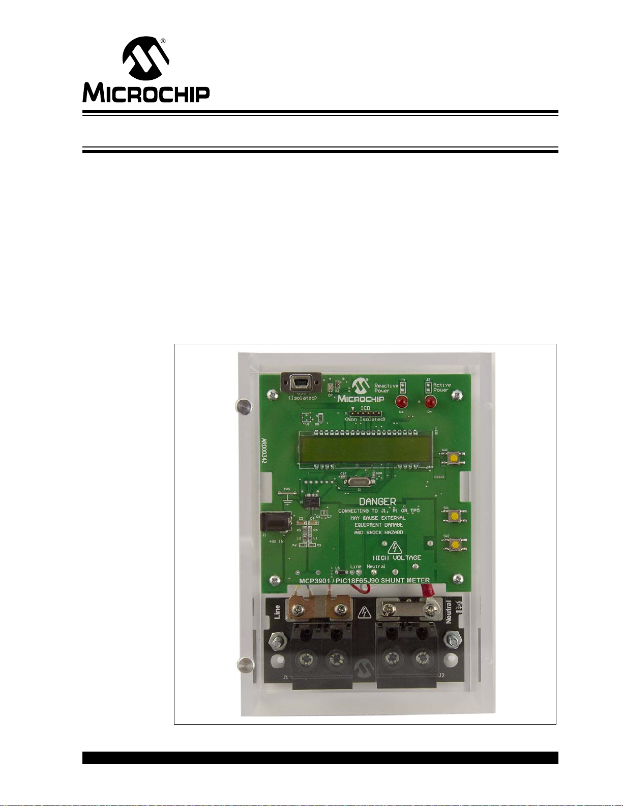
Chapter 1. Product Overview
1.1 INTRODUCTION
The MCP3901 and PIC18F65J90 Energy Meter Reference Design is a fully functional
IEC Class 0.5 compliant single-phase meter. This low-cost design does not use any
transformers and requires few external components. The PIC18F65J90 directly drives
the LCD, and includes both an isolated USB connection for meter calibration and
access to the device power calculations. The system calculates active energy, active
power, RMS current, RMS voltage, reactive energy, reactive power, apparent power
and other typical power quantities.
The Microchip Energy Meter 1-Phase Software is used to calibrate and monitor the
system, and can be used to create custom calibration setups. For some accuracy
requirements, only a single point calibration may be needed. The energy meter
software offers an automated step-by-step calibration process that can be used to
quickly calibrate energy meters.
MCP3901 AND PIC18F65J90
ENERGY METER
REFERENCE DESIGN
FIGURE 1-1: MCP3901 and PIC18F65J90 Single-Phase Energy Meter.
© 2012 Microchip Technology Inc. DS51968A-page 11
Page 12
MCP3901 and PIC18F65J90 Energy Meter Reference De sign
1.2 WHAT THE MCP3901 AND PIC18F65J90 ENERGY METER REFERENCE DESIGN KIT INCLUDES
This MCP3901 and PIC18F65J90 Energy Meter Reference Design kit includes:
• MCP3901 and PIC18F65J90 Energy Meter Reference Design User’s Guide
• Important Information Sheet
1.3 GETTING STARTED
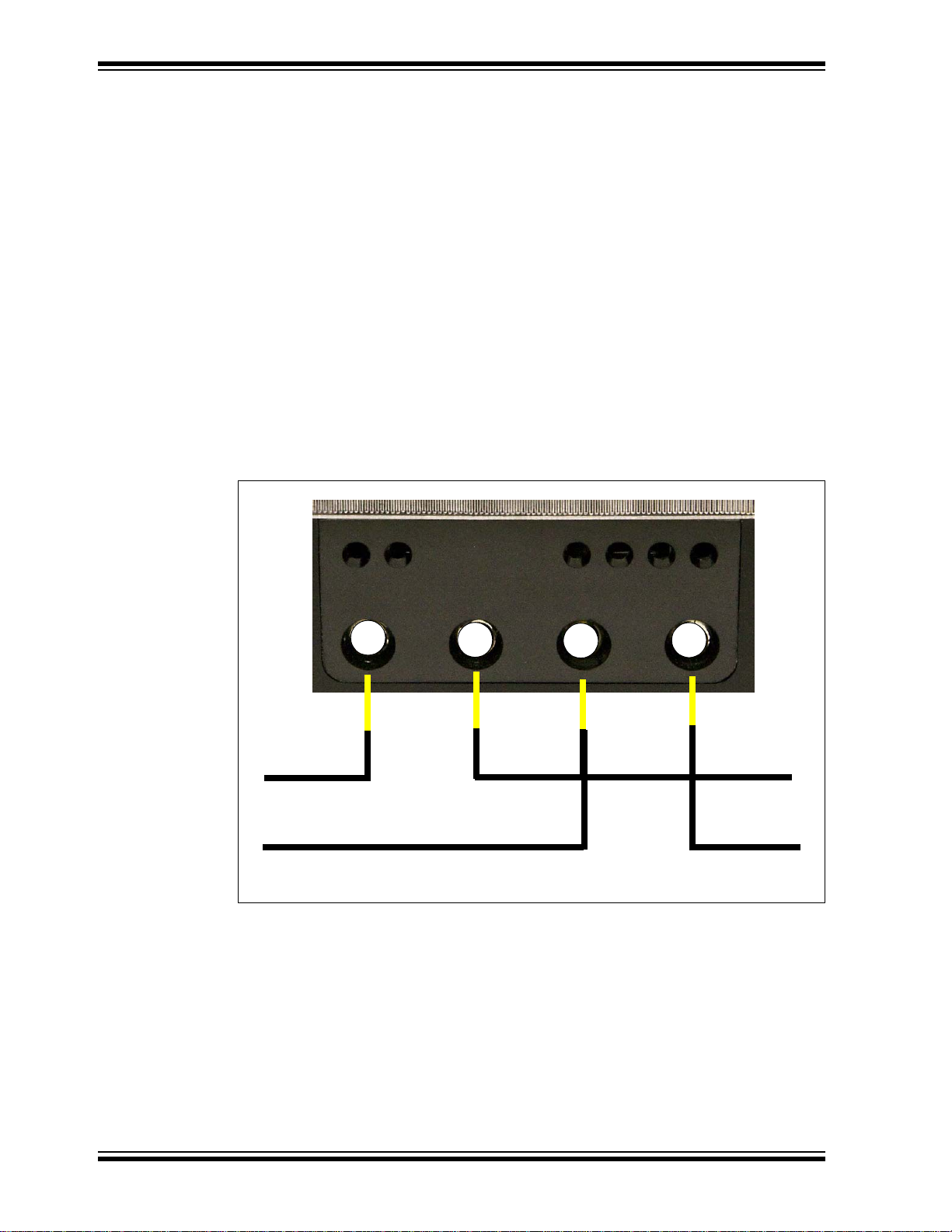
To describe how to use the MCP3901 and PIC18F65J90 Energy Meter Reference
Design, the following example is given using a two-wire 1-phase, 220 V AC line voltage
and connections using energy meter calibrator equipment, or other programmable load
source. The meter design uses a 5A load for calibration current, and a maximum
current (I
To test a calibrated meter, the following connections apply for a two-wire connection.
1.3.1 Step 1: Wiring Connections
Figure 1-2 identifies the line and load connections of the MCP3901 and PIC18F65J90
Energy Meter Reference Design.
MAX
) of 60A.
1
Line
Neutral
MAIN
2
3
4
Line
Neutral
LOAD
FIGURE 1-2: Example Connections using a 2-Wire System.
1.3.2 Step 2: Turn On Line/Load Power to the Meter (Power the Meter)
The meter will turn on when the line connection has 220V connected. The LCD display
will show the total energy accumulated.
DS51968A-page 12 © 2012 Microchip Technology Inc.
Page 13

2.1 OVERVIEW
Figures 2-1 and 2-2 show the MCP3901 and PIC18F65J90 and Energy Meter
Reference Design:
MCP3901 AND PIC18F65J90
ENERGY METER
REFERENCE DESIGN
Chapter 2. Hardware
3
1
4
2
10
J2
U1
LCD1
9
D9D8
D1
P1
D3
J4
J3
D2
SW3
8
7
SW1
C40
SW2
DANGER
HIGH VOLTAGE
MCP3901 / PIC18F65J90 SHUNT METER
Legend:
1 = IR for meter communication 7 = Push button Switches
2 = Test points 8 = 9-digit LCD Disp lay with icons for kWh and kVARh
3 = MCP3901 Analog Front End 9 = Pulse Output for Active and Reactive
4 = +9V DC Input (non-isolated) 10 = USB Connection (isolated)
5 = Connections to shunt
current sensing resistor
6 = Connections to Line and Neutral
5
6
(isolated)
FIGURE 2-1: Top View – Hardware Components.
© 2012 Microchip Technology Inc. DS51968A-page 13
Page 14
MCP3901 and PIC18F65J90 Energy Meter Reference De sign
.
17
C40
R21
R20
X2
R28
R27 R26
C32
C24 C25
R19
U7
R17
U4
C7
R29
U2
C39
R33
C37
U5
R30
R34
16
12
13
DANGER
HIGH VOLTAGE
C6
C5
C41
R14
R12
C2
R15
R11
C1
L1
Q1
C38
D5
D4
U8
C30
C27
C21
C22
C10
R31
C23
D6
L2
L3
R24 R25
C19
C17
R18
C16
D7
C4
MOV1
U6
C8
C9
R32
U3
Legend:
12 = Opto-isolators for Pulse outputs
13 = Power supply
14 = Non-volatile memory for calibration constants and energy usage data
15 = PIC18F65J90
16 = Isolation IC
17 = MCP2200 for USB connection
15
14
FIGURE 2-2: Bottom View – Hardware Components.
DS51968A-page 14 © 2012 Microchip Technology Inc.
Page 15
Hardware
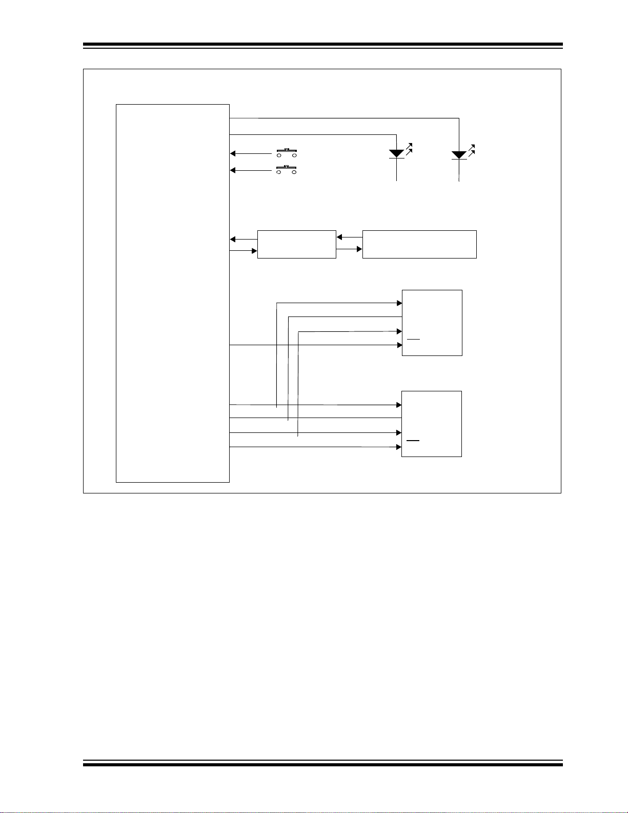
PIC18F65J90
RA2
RA3
RG1
RG4
RC7/RX
RC6/TX
RA5
RC3/SCK
RC4/SDI
RC5/SDO
RA1
SWITCH
SWITCH
USB to UART
Converter
MCP2200
Active
Power
Mini - USB Connector
(ISOLATED)
SCK
SDO
SDI
CS
MCP3901
AFE
SCK
SDO
SDI
CS
Reactive
Power
FIGURE 2-3: Digital Connections.
25LC256
SPI - EEPROM
© 2012 Microchip Technology Inc. DS51968A-page 15
Page 16

MCP3901 and PIC18F65J90 Energy Meter Reference De sign
2.2 INPUT AND ANALOG FRONT END
The MCP3901 and PIC18F65J90 and Energy Meter Reference Design comes
populated with components designed for 220V line voltage. At the bottom of the main
board are the high voltage line and neutral connections. There are four connections
that are made from the PCB to the meter casing. They are labeled LINE, NEUTRAL,
SHUNT1, and SHUNT2. The shunt sits on the high or line side of a two-wire system
and the meter employs a hot or “live” ground. The wires going into the shunt to
SHUNT1 and SHUNT2 should be twisted together. The wires going into the LINE and
NEUTRAL side of the meter should be twisted together, and also kept away from the
SHUNT1 and SHUNT2 wires if possible.
The neutral side of the two-wire system goes into a resistor divider on the voltage
channel input. Anti-aliasing low-pass filters will be included on both differential
channels. The voltage channel uses two 332 kΩ resistors to achieve a divider ratio of
664:1. For a line voltage of 230 V
490 mV
PEAK
.
, the channel 1 input signal size will be
RMS
LINE_SHUNT1
Shunt
(external to
PCB part of
meter case)
LINE_SHUNT2
NEUTRAL
150 FB (Note)
150 FB (Note)
332 kΩ
332 k Ω
1.0 kΩ
10-step optional
resistor
ladder
1.0 kΩ
1.0 kΩ
1.0 kΩ
Note: FB = ferrite beads. Ferrite beads have an impedance of the
specified value at 100 MHz.
CH0+
68 nF
CH0-
68 nF
MCP3901
0Ω
CH1+
68 nF
CH1+
68 nF
FIGURE 2-4: Analog Input Circuitry.
DS51968A-page 16 © 2012 Microchip Technology Inc.
Page 17

MCP3901 AND PIC18F65J90 ENERGY
METER REFERENCE DESIGN
Chapter 3. Calculation Engine and Register Description
3.1 CALCULATION ENGINE SIGNAL FLOW SUMMARY
RMS voltage, RMS current, Active Power, Reactive Power and Apparent Power, and
the calibration output pulse are all calculated through the following process described
in Figure 3-1. The calibration registers for each calculation are shown as well as the
16/24-bit
ADC
CURRENT
GAIN_
COMPENSATION
_90:
8
16/24-bit DS ADC
ADC
VOLTAGE
output registers.
ΔΣ
ADC
X
90°
with
Φ
Correction
Φ
OFFSET_I_RMS:
2
X
RMS Current
Reactive Power
O
FFSET_POWER_REACT:32
X
Active Power
PH
ASE_COMPENSATION:8
OFFSET_V_RMS:
OFFSET_POWER_ACT:
16
Σ
Σ
Σ
32
16
X
Apparent Power
8
NUMR_ENERGY_ACT:16
GAIN_
GAIN_DENR_ENERGY_ACT:
/
1/METER_CONSTAT
Σ
imp/kWh
DENR_ENERGY_REACT:8
GAIN_
imp/kVARh
Digital to
Frequency
Converter
Digital to
Frequency
Converter
NUMR_ENERGY_REACT:16
GAIN_
/
Σ
1/METER_CONSTAT
2
X
16
GAIN_POWER_REACT:
X
kVAR
32
POWER_REACT:
Σ
RMS Voltage
16
X
GAIN_ENERGY_REACT:
kVARh
REACT:32
ENERGY_
X
kVA
32
POWER_APP:
16
GAIN_ENERGY_ACT:
kWh
16
16
GAIN_V_RMS:
16
X
V
_RMS:16
V
X
GAIN_I_RMS:
GAIN_POWER_ACT:
A
_RMS:16
I
16
X
GAIN_POWER_APP:
kW
32
POWER_ACT:
16
XX
GAIN_ENERGY_APP:
kVAh
ACT:32
ENERGY_
APP:32
ENERGY_
FIGURE 3-1: PIC18F65J90 Calculation Engine Signal Flow
© 2012 Microchip Technology Inc. DS51968A-page 17
Page 18

MCP3901 and PIC18F65J90 Energy Meter Reference De sign
3.2 REGISTER LIST
Note: Important! Not all registers and features
are implemented in this version of
firmware release.
TABLE 3-1: INTERNAL REGISTER SUMMARY
Name Bits R/W Description
MODE 8 R/W Configuration register for operating mode of the meter
STATUS 8 R STATUS register
CAL_CONTROL 8 R/W Configuration register for calibration control
LINE_CYC 16 R/W 2n number of line cycles to be used during energy accumulation
LINE_CYC_CNT 16 R Counter for number of line cycles
2
RAW2_I_RMS 64 R Raw
RAW_I_RMS 16 R Raw RMS value from the current A/D converter in LSBs
I_RMS 16 R RMS value of the current, post Calibration
RAW2_V_RMS 64 R Raw
RAW_V_RMS 16 R Raw RMS value from the voltage A/D converter in LSBs
V_RMS 16 R RMS value of the voltage, post Calibration
LINE_FREQUENCY 16 R Line Frequency
RAW_POWER_ACT 64 R Raw Active Power
POWER_ACT 32 R Final Active Power, units in watts (W)
POWER_APP 32 R Final Apparent Power, units in volt-am peres (VA)
RAW_POWER_REACT 64 R Raw Reactive Power
POWER_REACT 32 R Final Reactive Power, units in volt-amperes-reactive (VAR)
PERIOD 32 R Period register
ENERGY_ACT 32 R Final Active Energy accumulated
RAW_ENERGY_ACT 64 R Raw Active Energy accumulated
ENERGY_APP 32 R Final Apparent Energy accu mulated
RAW_ENERGY_APP 64 R Raw Apparent Energy accumulated
I_ABS_MAX 8 R Not implemented
V_ABS_MAX 8 R Not implemented
ENERGY_REACT 32 R Final Reactive Energy accumulated
RAW_ENERGY_REACT 64 R Final Reactive Energy accumulated
PHASE_COMPENSATION 8 R/W Phase compensation between voltage and current
OFFSET_I_RMS 16 R/W Offset adjustment for RMS current reading
OFFSET_V_RMS 16 R/W Offset adjustment for RMS voltage reading
GAIN_I_RMS 16 R/W Gain adjustment for RMS current
GAIN_V_RMS 16 R/W Gain adjustment for RMS voltage
OFFSET_POWER_ACT 32 R/W Act ive Power offset
GAIN_POWER_ACT 16 R/W Ac tive Power gain adjust
OFFSET_POWER_REACT 32 R/W Offset correction for Reactive Power
GAIN_POWER_REACT 16 R/W Reactive Power gain adjust to produce X VAR/LSB
GAIN_ENERGY_ACT 16 R/W Not implemented
GAIN_ENERGY_APP 16 R/W Not implemented
GAIN_ENERGY_REACT 16 R/W Not implemented
CF_PULSE_WIDTH 8 R/W Defines CF pulse width from 0 to 255 x 0.8192 ms (0.209s)
GAIN_DENR_ENERGY_ACT 8 R/W Active Energy Pulse Output correction factor
RMS value from the current A/D converter in LSBs
2
RMS value from the voltage A/D converter in LSBs
DS51968A-page 18 © 2012 Microchip Technology Inc.
Page 19

Calculation Engi ne and Register Description
TABLE 3-1: INTERNAL REGISTER SUMMARY (CONTINUED)
Name Bits R/W Description
GAIN_NUMR_ENERGY_ACT 16 R/W Active Energy Pulse Output correction factor
MODE1_DEF 16 R/W Power Up Configuration Register
CAL_STATUS 16 R/W Calibration Status
MAXIMUM CURRENT 16 R/W Maximum current of the meter (I
CALIBRATION_VOLTAGE 16 R/W Calibration Voltage of the meter (V
CALIBRATION_CURRENT 16 R/W Calibration Current of the meter (I
CALIBRATION_FREQUENCY 16 R/W Calibration Frequency of the meter
METER_CONSTANT 16 R/W Meter Constant in imp/kWh or imp/kVARh
CALIBRATION_LINE_CYCLE 16 R/W Number of line cycles for calibration
GAIN_DENR_ENERGY_REACT 8 R/W Reactive Energy Pulse Output correction factor
GAIN_NUMR_ENERGY_REACT 16 R/W Reactive Energy Pulse Output correction factor
PHASE_COMPENSATION_90 8 R/W Phase delay for Reactive Power
CREEP_THRSHOLD_MINUTE 8 R/W No Load threshold time (minutes)
CREEP_THRSHOLD_SECOND 8 R/W No Load threshold time (seconds)
ENERGY_ACT 32 R/W Active Energy
ENERGY_REACT 32 R/W Reactive Energy
MAX
CAL
CAL
)
)
)
3.3 MODE
The MODE register controls the operation of the energy meter. The bit functions are
defined by the table below.
REGISTER 3-1: MODE REGISTER
U-0 U-0 U-0 U-0 R/W-0 R/W-0 R/W-0 R/W-0
— — — — CF ABSOLUTE PHASE CREEP
bit 7 bit 0
Legend:
R = Readable bit W = Writable bit U = Unimplemented bit, read as ‘0’
-n = Value at POR ‘1’ = Bit is set ‘0’ = Bit is cleared x = Bit is unknown
bit 7-4 Unimplemented: Read as ‘0’.
bit 3 CF: Active Energy CF Phase Enable bit
1 = Bit = 1 Phase is enabled to be accumulated into the total energy registers or CF pulse output
0 = Bit = 0 Phase is DISABLED and is not accumulated into the total energy registers or CF pulse
output
bit 2 ABSOLUTE Positive Only Energy Accumulation Mode bit
1 = Bit = 1 Positive energy only
0 = Bit = 0 Both negative and positive energy accumulated (negative energy is subtracted)
bit 1 PHASE: Phase bit
1 = Single-Point Phase Correction
0 = Multi-P oint Phase C orrection ( future)
bit 0 CREEP: No-Load Threshold bit
1 = Enabled
0 = Disabled
© 2012 Microchip Technology Inc. DS51968A-page 19
Page 20

MCP3901 and PIC18F65J90 Energy Meter Reference De sign
3.4 STATUS
The STATUS register contains the operational status of the energy meter. The bit
functions are defined in the table below.
REGISTER 3-2: STATUS REGISTER
U-0 U-0 U-0 U-0 U-0 U-0 R U-0
— — — — — —PH_S—
bit 7 bit 0
Legend:
R = Readable bit W = Writable bit U = Unimplemented bit, read as ‘0’
-n = Value at POR ‘1’ = Bit is set ‘0’ = Bit is cleared x = Bit is unknown
bit 7-2 Unimplemented: Read as ‘0’
bit 1 PH_S: Phase Sign bit
1 = CT may be in backward (if enabled)
0 = Operation normal
bit 0 Unimplemented: Read as ‘0’
3.5 CAL_CONTROL
This is the Calibration mode control register. Bit 0 enables the Calibration mode. In this
mode, the power meter operates as normal, but no updates are made to the voltage,
current, power or energy registers as long as bit 1 is low. When bit 1 is set high, the
registers are updated for LINE_CYC line cycles (only power and energy registers are
updated). After this time, bit 1 is set low by the PIC18F65J90 and the update of the
registers will stop. This allows the calibration software to set bit 0, clear the registers,
set bit 1 and start reading the desired registers, as well as the CAL_CONTROL register,
to check the status of bit 1. When bit 1 goes low, the LINE_CYC line cycles have
passed and the registers are final. Note that bit 0 takes effect immediately, and bit 1 will
take effect on the very next line cycle. When bit 1 goes low, all registers will be ready
to read.
REGISTER 3-3: CAL_CONTROL REGISTER (NOTE 1)
U-0 U-0 U-0 U-0 U-0 U-0 R/W-0 R/W-0
— — — — — Reserved CAL_UPDATE CAL_MODE
bit 7 bit 0
Legend:
R = Readable bit W = Writable bit U = Unimplemented bit, read as ‘0’
-n = Value at POR ‘1’ = Bit is set ‘0’ = Bit is cleared x = Bit is unknown
bit 7-3 Unimplemented: Read as ‘0’
bit 2 Reserved:
DS51968A-page 20 © 2012 Microchip Technology Inc.
Page 21

Calculation Engi ne and Register Description
REGISTER 3-3: CAL_CONTROL REGISTER (CONTINUED)(NOTE 1)
bit 1 CAL_UPDATE: Calibration Update bit
Power and energy registers upda ted for LINE _CYC lin e cy cl es when cle are d. Bit mu st be set for registers to begin updating, which starts on the next line cycle after bit is set.
1 = When the CAL_MODE bit is set, set the CAL_U PDA TE bit to enable update of power and energy
registers starting on next line cycle. Bit = 1 Single Point Phase Correction.
0 = When the CAL_MODE bit is set and the CAL_UPDATE bit has been set, the CAL_UPDATE bit
will be cleared after LINE_CYC line cycles. At that point, all registers will be updated and no
further updates will be done until the CAL_UPDATE bit is set again, or the CAL_MODE bit is
cleared.
bit 0 CAL_MODE: Calibration Mode bit
This bit enables Calibration mode.
1 = Calibration mode enabled
0 = Calibration mode disabled
Note 1: This register is used in Multi-Point and Single-Point Calibration modes only.
3.6 LINE_CYC
Name Bits Cof
LINE_CYC 16 R/W
Number of line cycles as a power of two. A setting of 0 indicates 20 or one line cycle.
A setting of 1 is two line cycles (2
of eight which is 256 line cycles. When written, this register will not take effect until the
previous number of line cycles has been acquired.
3.7 LINE_CYC_CNT
Name Bits Cof
LINE_CYC_CNT 16 R
This register counts from 0 and finishes at 2
LINE_CYC represents the value in the LINE_CYC register.
3.8 RAW2_I_RMS
Name Bits Cof
RAW2_I_RMS 64 R
This register is the square of the raw RMS value from the current A/D converter in
LSBs. By definition, this register will always contain a positive value, including the situation where power is negative from a backwards CT or otherwise. This register is
overwritten every LINE_CYC line cycle and is written only once, if calibration is
enabled.
1
), a setting of 2 is four lines cycles (22), up to a setting
(LINE_CYC - 1)
. Then it restarts at 0, where
© 2012 Microchip Technology Inc. DS51968A-page 21
Page 22

MCP3901 and PIC18F65J90 Energy Meter Reference De sign
3.9 RAW_I_RMS
Name Bits Cof
RAW_I_RMS 16 R
This register is the raw RMS value from the current A/D converter in LSBs (square root
of the top 32-bits of RAW2_I_RMS + OFFSET_I_RMS). By definition, this register will
always contain a positive value (even if the CT is in backwards). This register is overwritten every LINE_CYC line cycle and is written only once, if calibration is enabled.
3.10 I_RMS
Name Bits Cof
I_RMS 16 R
This register is the RMS value of phase A current in X A/LSB, as determined by the
value in the GAIN _I_RMS regist er . When display ing the RMS curr ent, multiply the (decimal) value in these registers by X to get the display value in amperes. This register is
overwritten every LINE_CYC line cycle (written only once if calibration is enabled).
3.11 RAW2_V_RMS
Name Bits Cof
RAW2_V_RMS 64 R
This register is the square of the raw RMS value from the voltage A/D converter in
LSBs. By definition, it will always contain a positive value. This register is overwritten
every LINE_CYC line cycle (written only once if calibration is enabled).
3.12 RAW_V_RMS
Name Bits Cof
RAW_V_RMS 16 R
This is the raw RMS value from the voltage A/D converter in LSBs (square root of the
top 32-bits of RAW2_V_RMS + OFFSET_V_RMS). By definition, this register will
always contain a positive value. The register is overwritten every LINE_CYC line cycle
(written only once if calibration is enabled).
3.13 V_RMS
Name Bits Cof
V_RMS 16 R
This register is the RMS value of the voltage, in X 0.01 V/LSB, as determined by the
value in the GAIN_V_RMS register. When displaying the RMS voltage, assume a calibrated meter exists and multiply the (decimal) value in these registers by X to get the
display value in volts. This register is overwritten every LINE_CYC line cycle (written
only once if calibration is enabled).
DS51968A-page 22 © 2012 Microchip Technology Inc.
Page 23

Calculation Engi ne and Register Description
3.14 LINE_FREQUENCY
Name Bits Cof
LINE_FREQUENCY 16 R
This register holds the measured line frequency using the zero crossing technique.
3.15 RAW_POWER_ACT
Name Bits Cof
RAW_POWER_ACT 64 R
This register is the raw active power, as it represents the sum of current A/D value times
voltage A/D value results over LINE_CYC line cycles (each line cycle has 128 results).
Each current times voltage multiplication results in a 32-bit word. There are up to 256
line cycles with each line cycle being 128 results, and each result being 32-bit. Thus,
48 bits are needed. This is the register to be read during calibration for calculating the
offset and gain values associated with active power, OFFSET_POWER_ACT and
GAIN_POWER_ACT. This register is overwritten every line cycle, however if calibration
is enabled, the updates will stop once the LINE_CYC line cycles have elapsed.
3.16 POWER_ACT
Name Bits Cof
POWER_ACT 32 R
This register is the value for active power. The goal of the calibration is to get this register value to equal X W/LSB. This is done with the OFFSET_POWER_ACT and
GAIN_POWER_ACT registers. When displaying the power, multiply the (decimal)
value in this register by X to get the display value in watts. This register is overwritten
every LINE_CYC line cycle (written only once if calibration is enabled).
3.17 POWER_APP
Name Bits Cof
POWER_APP 32 R
This is the value of the apparent power. The goal of the calibration is to get this value
to equal X VA/LSB. This is done with the GAIN_POWER_APP registers. When displaying the power for phase A, multiply the (decimal) value in this register by X to get the
display value in watts. This register is overwritten every LINE_CYC line cycle (written
only once if calibration is enabled).
© 2012 Microchip Technology Inc. DS51968A-page 23
Page 24

MCP3901 and PIC18F65J90 Energy Meter Reference De sign
3.18 RAW_POWER_REACT
Name Bits Cof
RAW_POWER_REACT 64 R
This is the raw reactive power. This register is read during the calibration for calculating
the gain values associated with the reactive power and GAIN_POWER_REACT. This
register is overwritten every LINE_CYC line cycle (written only once if calibration is
enabled). This register is accumulated on a line-cycle basis.
3.19 POWER_REACT
Name Bits Cof
POWER_REACT 32 R
This is the value for reactive power. The goal is to get this value to equal X VAR/LSB.
This is done with the GAIN_POWER_REACT register. When displaying the power,
multiply the (decimal) value in this register by X to get the display value in watts. This
register is overwritten every LINE_CYC line cycle (written only once if calibration is
enabled).
3.20 PERIOD
Name Bits Cof
PERIOD 32 R
This 32-bit register represents the total number of clock ticks that elapsed over the most
recent LINE_CYC line cycle. Each LSB represents 1.6 µs with a 4 MHz clock on the
microcontroller. This register is overwritten every LINE_CYC line cycle (written only
once if calibration is enabled).
3.21 ENERGY_ACT
Name Bits Cof
ENERGY_ACT 32 R
RAW_ENERGY_ACT 64 R
The design updates the Energy register using the CF Pulse blink output count. In this
method, the Energy registers increments every pulse by a value equal to
1/(METER_CONSTANT).
ENERGY_ACT = ENERGY_ACT + (1/METER_CONSTANT)
The gain calibration registers GAIN_NUMR_ENERGY_ACT and
GAIN_DENR_ENERGY_ACT operate the same for this method also.
DS51968A-page 24 © 2012 Microchip Technology Inc.
Page 25

Calculation Engi ne and Register Description
3.22 ENERGY_APP
Name Bits Cof
ENERGY_APP 32 R
RAW_ENERGY_APP 64 R
These two registers represent the total apparent energy accumulated so far.
3.23 I_ABS_MAX
Name Bits Cof
I_ABS_MAX 8 R
NOT IMPLEMENTED IN THIS FIRMWARE/SOFTWARE RELEASE.
3.24 V_ABS_MAX
Name Bits Cof
V_ABS_MAX 8 R/W
NOT IMPLEMENTED IN THIS FIRMWARE/SOFTWARE RELEASE.
3.25 ENERGY_REACT
Name Bits Cof
ENERGY_REACT 32 R
RAW_ENERGY_REACT 64 R
The design updates the reactive energy register using the CF Pulse blink output. In this
method, the Energy registers increment every pulse by a value equal to
1/(METER_CONSTANT).
ENERGY_REACT = ENERGY_REACT + (1/METER_CONSTANT)
The gain calibration registers GAIN_NUMR_ENERGY_ACT and
GAIN_DENR_ENERGY_ACT operate the same for this method also.
3.26 PHASE_COMPENSATION
Name Bits Cof
PHASE_COMPENSATION 8 R/W
Phase delay, signed 8-bit value, provides the phase compensation by sampling time/2.
© 2012 Microchip Technology Inc. DS51968A-page 25
Page 26

MCP3901 and PIC18F65J90 Energy Meter Reference De sign
3.27 OFFSET_I_RMS
Name Bits Cof
OFFSET_I_RMS 16 R/W
Square of the offset for RMS current reading, signed 16-bit value. Note that this value
should be similar to the ADC’s noise squared. At a gain of 1, the noise will be about
1 LSB, 2 LSBs at a gain of 2, 6 LSBs at a gain of 8, 11 LSBs at a gain of 16, and
22 LSBs at a gain of 32. There may be other sources of noise. Using the square of the
offset allows for higher accuracy. The value will be added before the square root is
taken when calculating the final RMS value.
3.28 OFFSET_V_RMS
Name Bits Cof
OFFSET_V_RMS 16 R/W
Square of offset for RMS voltage reading, signed 8-bit value. Note that this value
should be similar to the ADC’s noise squared. For the voltage channel, the noise will
be about 1 LSB. There may be other sources of noise. Using the square of the offset
allows for higher accuracy. The value will be added before the square root is taken
when calculating the final RMS value.
3.29 GAIN_I_RMS
Name Bits Cof
GAIN_I_RMS 16 R/W
Current gain to produce X A/LSB. The value is always less than one (for example,
32,767 = 0.9999695).
3.30 GAIN_V_RMS
Name Bits Cof
GAIN_V_RMS 16 R/W
Voltage gain to produce 0.1 V/LSB in the V_RMS register. The value is always less than
one (for example, 32,767 = 0.9999695).
3.31 OFFSET_POWER_ACT
Name Bits Cof
OFFSET_POWER_ACT 32 R/W
Active power offset (this is a straight offset, not the square, as with voltage and current).
A much larger value is needed because the power is a running sum. This is a 32-bit
signed value.
DS51968A-page 26 © 2012 Microchip Technology Inc.
Page 27

Calculation Engi ne and Register Description
3.32 GAIN_POWER_ACT
Name Bits Cof
GAIN_POWER_ACT 16 R/W
Active power gain to produce X W/LSB. The value is always less than one (for example,
32,767 = 0.9999695).
3.33 OFFSET_POWER_REACT
Name Bits Cof
OFFSET_POWER_REACT 32 R/W
Reactive power offset (this is a straight offset, not the square, as with voltage and current). A much larger value is needed because the power is a running sum. This is a
32-bit signed value.
3.34 GAIN_POWER_REACT
Name Bits Cof
GAIN_POWER_REACT 16 R/W
Reactive power gain to produce X W/LSB. The value is always less than one (for example, 32,767 = 0.9999695).
3.35 GAIN_ENERGY_ACT
Name Bits Cof
GAIN_ENERGY_ACT 16 R/W
Active energy gain to produce X Wh/LSB. The value is always less than one (for example, 32,767 = 0.9999695).
3.36 GAIN_ENERGY_APP
Name Bits Cof
GAIN_ENERGY_APP 16 R/W
Apparent energy gain to produce X VAh/LSB. The value is always less than one (for
example, 32,767 = 0.9999695).
3.37 GAIN_ENERGY_REACT
Name Bits Cof
GAIN_ENERGY_REACT 16 R/W
Reactive energy gain to produce X VARh/LSB. The value is always less than one (for
example, 32,767 = 0.9999695).
© 2012 Microchip Technology Inc. DS51968A-page 27
Page 28

MCP3901 and PIC18F65J90 Energy Meter Reference De sign
3.38 CF_PULSE_WIDTH
Name Bits Cof
CF_PULSE_WIDTH 8 R/W
Defines the CF pulse width from 0 to 255. Length of width is valued
* 8 * (1/LINE_FREQUENCY)/128) ms. A maximum of 0.266 seconds for 60 Hz and
0.319 seconds for 50 Hz.
If the value is 0, no CF pulse is produced.
3.39 GAIN_DENR_ENERGY_ACT
Name Bits Cof
GAIN_DENR_ENERGY_ACT 8 R/W
8-bit signed value. Represents the number of shifts for active power energy register
ENERGY_ACT before GAIN_DENR_ENERGY_ACT is applied.
3.40 GAIN_NUMR_ENERGY_ACT
Name Bits Cof
GAIN_NUMR_ENERGY_ACT 16 R/W
Active power gain to produce a specified pulses per watt-hour. The value is always less
than one (for example, 32,767 = 0.9999695).
3.41 MODE1_DEF
Name Bits Cof
MODE1_DEF 16 R/W
MODE default power-up settings. On power-up, this register will be read and placed
into the MODE register.
3.42 CAL_STATUS
The CAL_STATUS register holds the calibration status for each individual phase.
Broken down by phase, these are the values that can be calibrated. Each bit has the
status of 0 = NOT Calibrated, 1 =Calibrated.
REGISTER 3-4: CAL_STATUS REGISTER
R/W-0 R/W-0 R/W-0 U-0 U-0 R/W-0 R/W-0 R/W-0
PHASE_COM
PENSATION
bit 15 bit 8
OFFSET_I_
RMS
OFFSET_V_
RMS
— — GAIN_I_RMS GAIN_V_RMS OFFSET_PO
WER_ACT
U-0 R/W-0 U-0 U-0 U-0 R/W-0 U-0 U-0
— GAIN_POW
ER_ACT
bit 7 bit 0
DS51968A-page 28 © 2012 Microchip Technology Inc.
— — — GAIN_POWE
R_REACT
— —
Page 29

Calculation Engi ne and Register Description
REGISTER 3-4: CAL_STATUS REGISTER (CONTINUED)
Legend:
R = Readable bit W = Writable bit U = Unimplemented bit, read as ‘0’
-n = Value at POR ‘1’ = Bit is set ‘0’ = Bit is cleared x = Bit is unknown
bit 15-0 All bits: Calibration Register Status bits
1 = This register has been calibrated
0 = This register is NOT calibrated
3.43 MAXIMUM CURRENT
Name Bits Cof
MAXIMUM_CURRENT 16 R/W
This register holds the maximum current for the meter (I
3.44 CALIBRATION_VOLTAGE
Name Bits Cof
CALIBRATION_VOLTAGE 16 R/W
This register holds the calibration voltage of the meter (V
3.45 CALIBRATION_CURRENT
Name Bits Cof
CALIBRATION_CURRENT 16 R/W
This register holds the calibration current of the meter (I
3.46 CALIBRATION_FREQUENCY
Name Bits Cof
CALIBRATION_FREQUENCY 16 R/W
MAX
CAL
CAL
).
).
).
This register holds the calibration frequency of the meter.
3.47 METER_CONSTANT
Name Bits Cof
METER_CONSTANT 16 R/W
This register holds the meter constant in imp/kWh or imp/kVARh.
© 2012 Microchip Technology Inc. DS51968A-page 29
Page 30

MCP3901 and PIC18F65J90 Energy Meter Reference De sign
3.48 CALIBRATION_LINE_CYCLE
Name Bits Cof
CALIBRATION_FREQUENCY 16 R/W
This register holds the number of line cycles used during the calibration.
3.49 GAIN_DENR_ENERGY_REACT
Name Bits Cof
GAIN_DENR_ENERGY_REACT 8 R/W
8-bit signed value. Represents the number of shifts for reactive power energy register,
before GAIN_NUMR_ENERGY_REACT is applied.
3.50 GAIN_NUMR_ENERGY_REACT
Name Bits Cof
GAIN_NUMR_ENERGY_REACT 16 R/W
Reactive power gain to produce a specified pulse per VAR-hour. The value is always
less than one (for example, 32,767 = 0.9999695).
3.51 PHASE_COMPENSATION_90
Name Bits Cof
PHASE_COMPENSATION_90 8 R/W
Phase delay for reactive power, signed 8-bit value, sampling time/2.
3.52 CREEP_THRSHOLD_MINUTE
Name Bits Cof
CREEP_THRSHOLD_MINUTE 8 R/W
This 8-bit register holds the decimal representation of the creep threshold time in
minutes (total creep is minutes + seconds register).
3.53 CREEP_THRSHOLD_SECOND
Name Bits Cof
CREEP_THRSHOLD_SECOND 8 R/W
This 8-bit register holds the decimal representation of the creep threshold time in
seconds (total creep is minutes + seconds register).
DS51968A-page 30 © 2012 Microchip Technology Inc.
Page 31

Chapter 4. Meter Protocol and Timings
4.1 PROTOCOL
The Universal Asynchronous Receiver/Transmitter (UART) of the PIC18F65J90 is
used to access the register map of the meter. In addition to the reading and writing of
the registers, there are also dedicated commands for clearing calibration registers,
loading calibration registers and storing calibration registers to flash. The first byte
UART data is an ASCII character that represents the command, and each command
has a specific protocol. Each command ends with the ASCII character “X”.
4.1.1 Command Description
The first byte of the data (byte 0) is an ASCII character E, L, S, W and R.
• E – Echo All Data Received (ECHO)
• L – Load Calibration Registers from Flash (LOAD)
• S – Store Calibration Registers (STORE)
• W – Write Bytes (WRITE)
• R – Read Bytes (READ)
The last data byte is always an 'X' character. All commands will result in the same
command being returned. The exception is the 'R' (read) command which will return
additional data in lieu of the number of bytes.
MCP3901 AND PIC18F65J90
ENERGY METER
REFERENCE DESIGN
4.1.1.1 “E” ECHO: - ECHO ALL DATA RECEIVED
Example: 'EABCDEFGHIJKLMNOPQRSTUVWYZ1234567890X'.
Returns: 'EABCDEFGHIJKLMNOPQRSTUVWYZ1234567890X'.
4.1.1.2 “L” LOAD: LOAD CALIBRATION REGISTERS FROM FLASH.
Example: 'LX'.
Returns: 'LX'.
This command is used to verify that the calibration values were actually written into
flash (or E EPROM) . Once the so f twa re exe cut es a 'SX' comman d, it shou ld v erif y th at
the values were stored by issuing an 'LX' command and then reading the calibration
values with a 'R' command.
4.1.1.3 “S” STORE: STORE CALIBRATION REGISTERS INTO FLASH
Note that the store command will write all calibration values to internal EEPROM, and
this function takes some time. During that time, the meter is not functional. The store
command should only be used after calibrating the meter, and not while it is in actual
use.
Example: 'SX'.
Returns: 'SX'.
© 2012 Microchip Technology Inc. DS51968A-page 31
Page 32

MCP3901 and PIC18F65J90 Energy Meter Reference De sign
4.1.1.4 “W” WRITE: WRITE STARTING AT SPECIFIED ADDRESS
Write specified bytes.
Example: 'W030000102030405060708090A0B0C0D0E0FX'.
Returns: 'W030000102030405060708090A0B0C0D0E0FX'.
Note: If the number of data characters is odd, the last character (the one just prior
to the 'X') will be ignored.
Command Byte
76543210
ASCII Data
76543210
6543210
7
TABLE 4-1: WRITE COMMAND EXAMPLES
Description Command ASCII Command Hex
WRITE of 255d to
PHA_W_OFF Register
“W 170 00 F F X” 57 31 37 30 30 30 46 46 58
FIGURE 4-1: WRITE Command Protocol.
4.1.1.5 “R” READ: READ STARTING AT SPECIFIED ADDRESS
Example: 'R03010X' (read 16 bytes starting at address 30h).
Returns: 'R030000102030405060708090A0B0C0D0E0FX'
Note: For 16 bytes, there are 32 ASCII characters returned, or two characters per
byte.
3 Address Bytes (ASCII)
543210
76
“X” (ASCII)
76543210
7654321076543210
Command Byte
76543210
# Bytes to Read (2 Bytes ASCII)
76543210
76543210
76543210
3 Address Bytes (ASCII)
76543210 76543210
“X” (ASCII)
76543210
TABLE 4-2: READ COMMAND EXAMPLES
DESCRIPTION COMMAND ASCII COMMAND HEX
READ on ENERGY_ACT_L_RAW Register “R 0D4 06 X” 52 00 44 34 30 36 58
FIGURE 4-2: Read Command Protocol.
DS51968A-page 32 © 2012 Microchip Technology Inc.
Page 33

Appendix A. Schematic and Layouts
A.1 INTRODUCTION
This appendix contains the following schematics and layouts for the MCP3901 and
PIC18F65J90 Energy Meter Reference Design:
• Board – ADC Schematic
• Board – MCU Schematic
• Board – LCD and USB Schematic
• Board – Top Silk and Pads
• Board – Top Copper
• Board – Bottom Copper
• Board – Bottom Silk and Pads
• Board – Top 3D
• Board – Bottom 3D
MCP3901 AND PIC18F65J90
ENERGY METER
REFERENCE DESIGN
A.2 SCHEMATICS AND PCB LAYOUT
The layer order is shown in Figure A-1.
FIGURE A-1: Layer Order.
Top Layer
Bottom Layer
© 2011 Microchip Technology Inc. DS51968A-page 33
Page 34

MCP3901 and PIC18F65J90 Energy Meter Reference De sign
A.3 BOARD – ADC SCHEMATIC
TP5
(LOW)
(LOW)
TP3
TP1
TP2
MPU_SDO
MPU_SCK
AFE_F0/CS
TP6
TP4
TP7
MPU_SDI
AFE_SYNC
AFE_CLKIN
GNDA
!!! DANGER!!!
AND SHOCK HAZARD
EQUIPMENT DAMAGE
MAY CAUSE EXTERNAL
CONNECTING TO J1, P1 or TP5
+3.3V
CAP-SMT-ELECTRO
C10
10uF
GNDB
C15
100nF
GNDB
OUT
GND
Q1
1
GNDB
IN
MCP1700T-3302E/TT
32
+5V
+5V
AFE_CLKIN
AFE_DR
141516
DR
OSC2
OSC1/CLKI
CH1+
CH1-
CH0-
6
7
NPO
NPO
NPO
100nF
NONE
CP2
13
12
MDAT1
MDAT0
AGND
REFIN/OUT+
8
9
GNDA
C5
100nF
R7
1K
C4
100nF
C3
GNDA
GNDB
11
DGND
REFIN
10
GNDA
GNDA
SSOP20
MCP3901
GNDAGNDA
GNDA
R9
332K
R8
332K
L3
300mA/150
100nF
100nF
NPO
100nF
R10
GNDB
C14
100nF
+5V +5V
C13
10UF
GNDB
C12
100nF
GNDB
3
OUT
C7
GNDA
C6
U2
MCP1703
GND
2
IN
1
GNDA
L5
150
GNDB
GNDA
C11
470UF
1
D1
2
MRA4005T3G
3
1
2
POWER
GNDA
C8
+9V IN
LOW
RAPC722
J1
D2
21
MRA4005T3G
R11
100
C9
GNDA
1K
L4
150 0.47uF
GNDB
GNDB
D3
BZG03C15G
GNDB
MOV1
HIGH
275VAC
CP4
CP5
GNDB
MPU_SCK
MPU_SDO
MPU_SDI
AFE_F0/CS
20
19
17
18
CS
SDI
SDO
SCK
U1
CH0+
RESET
DVDD
AVDD
12345
R2
10
10
AFE_SYNC
C2
100nF
R1
GNDB
GNDA
C1
100nF
R4
R5
1K TF
1K TF
L2
L1
300mA/150
300mA/150
GNDA
R3
NONE
R6
CP1
CP3
Shunt GND
LINE_SHUNT2
LINE_SHUNT1
HIGH
DS51968A-page 34 © 2011 Microchip Technology Inc.
Page 35

A.4 BOARD – MCU SCHEMATIC
Schematic and Layouts
GNDB
+3.3V
+3.3V
+3.3V
+3.3V
+3.3V
100NF
100NF
100NF
100NF
47NF
R12
R17
+3.3V
P1
HDR6X1
C20
GNDB
C19
GNDB
C18
GNDB
C17
GNDB
LCD_4A/4F/4E/4D
49
LCD_4B/4G/4C/4P
50
LCD_3A/3F/3E/3D
51
LCD_1A/1F/1E/1D
52
LCD_2B/2G/2C/2P
53
LCD_2A/2F/2E/2D
54
LCD_3B/3G/3C/3P
55
56
GNDB
+3.3V
57
LCD_1B/1G/1C/1P
58
LCD_V/K2/R/H2
59
LCD_COM4
60
LCD_COM3
61
LCD_COM2
62
LCD_COM1
63
64
C16
NONE
10K
DD
1
VSS
V
MPU_MCLR
GNDB
+3.3V
234
484746
RD7/SEG7
RD6/SEG6
RD5/SEG5
RD4/SEG4
RD3/SEG3
RD2/SEG2
RD1/SEG1
RD0/SEG0
/SEG31
(1)
RE6/COM3
RE5/COM2
RE4/COM1
RE3/COM0
LCDBIAS3
1
C21
47NF
MPU_PGD
MPU_PGC
ICD
5
6
PIC18F65J90
AFE_DR
LCD_5A/5F/RE/5D
LCD_5B/5G/5C/NC
LCD_6B/6G/6C/NC
454443
RB2/INT2/SEG9
RB1/INT1/SEG8
RB0/INT0/SEG30
RB3/INT3/SEG10
RE7/CCP2
RG1/TX2/CK2
RG0/LCDBIAS0
RE1/LCDBIAS2
RE0/LCDBIAS1
4
3
2
C22
47NF
C23
MPU_RG1
47NF
GNDB
GNDB
GNDB
GNDB
SW1
+3.3V
B3S-1002P
R13
4.7K
R14
100NF
1K
MPU_RG4
X1
4MHz
GNDB
MPU_PGC
LCD_7B/7G/7C/NC
LCD_6A/6F/6E/6D
39
424140
SS
V
RB6/KBI2/PGC
RB4/KBI0/SEG11
RB5/KBI1/SEG29
OSC2/CLKO/RA6
U3
PIC18F6XJ90-64TQFP
SS
VDDCORE/VCAP
V
RG4/SEG26
MCLR
RG2/RX2/DT2/VLCAP1
RG3/VLCAP2
7
5
6
9
8
10
MPU_RG4
MPU_MCLR
GNDB
10UF
C26
47NF C24
MOM-NC
PUSH=HI
+3.3V
GNDB
R15
4.7K
C25
27pF
C28
GNDB
GNDB
GNDB
C27
27pF
MPU_SDO
MPU_SDI
MPU_PGD
+3.3V
383736
353433
VDD
RB7/KBI3/PGD
OSC1/CLKI/RA7
RC5/SDO/SEG12
RC4/SDI/SDA/SEG16
RF6/AN11/SEG24
RF4/AN9/SEG22
RF5/AN10/CVREF/SEG23
RF7/AN5/SS/SEG25
11
13
12
14
LCD_9A/0F/9E/9D
GNDB
LCD_9B/9F/9E/NC
LCD_10A/10F/10E/10D
LCD_10B/10G/AOC/NC
GNDB
MOM-NC
PUSH=HI
SW2
B3S-1002P
GNDB
C29
R16
100NF
1K
MPU_RG1
MPU_SCK
AFE_CLKIN
RC2/CCP1/SEG13
RC3/SCK/SCL/SEG17
RF3/AN8/SEG21
RF2/AN7/C1OUT/SEG20
16
15
LCD_8A/8F/8E/8D
LCD_8B/8G/8C/NC
IR_TX
698
R20
REF
DD
+3.3V
100NF
+3.3V
U8
GNDB
D5
GP1US301XP
GL100MN1MP1
RC7/RX1/DT1/SEG28
RC6/TX1/CK1/SEG27
RC0/T1OSO/T13CKI
RC1/T1OSI/CCP2/SEG12
RA4/T0CKI/SEG14
RA5/AN4/SEG15
VDD
V
SS
RA0/AN0
RA1/AN1/SEG18
RA2/AN2//V
RA3/AN3/VREF+
AVSS
AV
ENVREG
RF1/AN6/C2OUT/SEG19
MPU_RX1
32
MPU_TX1
31
IR_TX
30
29
IR_RX
28
27
26
25
24
23
22
21
20
19
18
+3.3V
GNDB
GNDB
+3.3V
+3.3V
AFE_F0/CS
AFE_SYNC
MEM_CS
17
GNDB
C32
IR_RX
2
3
GNDB
41
LCD_V/K1/H1/A/W
CF_REACTIVE
CF_ACTIVE
LCD_7A/7F/7E/7D
GNDB
DNP
U6
PC365N
698
R19
D4
R18
1.2k
CF_ACTIVE
GNDB
SW3
B3S-1002P
U5
MCP130
MCP130T-270/TT
+3.3V
7
8
VCC
U4
CS
1
2
25LC256-I/SM
MEM_CS
+3.3V
2
1
HDR2X1
4
3
1
2
GNDB
RED
GM1JR35200AE
GNDB
ACTIVE PWR
MPU_MCLR
C31
1
VSS
OUT
3
VDD
2
+3.3V
MPU_SCK
+3.3V
5
6
SCK
HOLD
WP
SO
3
4
+3.3V
MPU_SDI
C30
100NF
J2
R22
CF_REACTIVE
100NF
MPU_SDO
SI
VSS
GNDB
GNDB
4
U7
PC365N
1
698
D6
R21
1.2k
GNDB
GNDB
DNP
2
1
J3
HDR2X1
3
2
GNDB
RED
GM1JR35200AE
GNDB
REACTIVE PWR
© 2011 Microchip Technology Inc. DS51968A-page 35
Page 36

MCP3901 and PIC18F65J90 Energy Meter Reference De sign
A.5 BOARD – LCD AND USB SCHEMATIC
LCD
LCD_3B/3G/3C/3P
20
LCD_3A/3F/3E/3D
19
LCD_4B/4G/4C/4P
18
LCD_4A/4F/4E/4D
17
LCD_5B/5G/5C/NC
16
LCD_5A/5F/RE/5D
15
LCD_6B/6G/6C/NC
14
LCD_6A/6F/6E/6D
13
LCD_7B/7G/7C/NC
12
LCD_7A/7F/7E/7D
11
LCD_8B/8G/8C/NC
10
LCD_8A/8F/8E/8D
9
LCD_9B/9F/9E/NC
8
LCD_9A/0F/9E/9D
7
LCD_10B/10G/AOC/NC
6
LCD_10A/10F/10E/10D
5
LCD_11B/11G/11C/NC
4
LCD_11A/AAF/11E/11D
3
LCD_V/K2/R/H2
2
LCD_V/K1/H1/A/W
1
3B/3G/3C/3P
3A/3F/3E/3D
4B/4G/4C/4P
4A/4F/4E/4D
5A/5F/5E/5D
6A/6F/6E/6D
7A/7F/7E/7D
8A/8F/8E/8D
9A/9F/9E/9D
V/K2/r/h2
K1h1/A/W
5B/5G/5C/NC
6B/6G/6C/NC
7B/7G/7C/NC
8B/8G/8C/NC
9B/9G/9C/NC
10B/10G/10C/NC
10A/10F/10E/10D
11B/11G/11C/NC
11A/11F/11E/11D
2A/2F/2E/2D
21
2B/2G/2C/2P
22
1A/1F/1E/1D
23
1B/1G/1C/1P
24
COM1
25
COM2
26
COM3
27
COM4
28
LCD_2A/2F/2E/2D
LCD_2B/2G/2C/2P
LCD_1A/1F/1E/1D
LCD_1B/1G/1C/1P
U9
LCD_COM1
LCD_COM2
LCD_COM3
LCD_COM4
2
1
USB_+5V
C33
D-
0.1uF
3
D+
470
R23
GND
!!! DANGER !!!
AND SHOCK HAZARD
EQUIPMENT DAMAGE
MAY CAUSE EXTERNAL
CONNECTING TO J1, P1, J2 OR TP1
USB_MINIB_VERTICAL
7
6
4
5
GND
D+
D-
VSS
U10
VDD
OSC1
OSC2
GND
C34
0.1uF
VUSB
GP0/SSPND
GP1/USBCFG
RST
GP7/TxLED
GP6/RxLED
+3.3V
U11
GP2
GP5
MPU_TX1
VDD2VDD1
RX
CTS
GP4
GP3
MPU_RX1
VIA
VOB
GND2
VOA
GND1
ADUM1201
VIB
MCP2200_RX
MCP2200_TX
RTS
MCP2200_SSOP20
TX
R25
470
2
3
470
R24
GNDB
GND
GND
+3.3V
D7
100NF
RED
1
4
GREEN
C35
GNDB
USB_+5V
LCD1
INDIA LCD
X2
RESONATOR-CSTCE
12 MHz
GND
DS51968A-page 36 © 2011 Microchip Technology Inc.
Page 37

A.6 BOARD – TOP SILK AND PADS
Schematic and Layouts
© 2011 Microchip Technology Inc. DS51968A-page 37
Page 38

MCP3901 and PIC18F65J90 Energy Meter Reference De sign
A.7 BOARD – TOP COPPER
DS51968A-page 38 © 2011 Microchip Technology Inc.
Page 39

A.8 BOARD – BOTTOM COPPER
Schematic and Layouts
© 2011 Microchip Technology Inc. DS51968A-page 39
Page 40

MCP3901 and PIC18F65J90 Energy Meter Reference De sign
A.9 BOARD – BOTTOM SILK AND PADS
DS51968A-page 40 © 2011 Microchip Technology Inc.
Page 41

A.10 BOARD – TOP 3D
Schematic and Layouts
© 2011 Microchip Technology Inc. DS51968A-page 41
Page 42

MCP3901 and PIC18F65J90 Energy Meter Reference De sign
A.11 BOARD – BOTTOM 3D
DS51968A-page 42 © 2011 Microchip Technology Inc.
Page 43

MCP3901 AND PIC18F65J90
ENERGY METER
REFERENCE DESIGN
Appendix B. Bill of Materials (BOM)
TABLE B-1: BILL OF MATERIALS (BOM)
Qty Refe rence Description Manufac turer Part Number
20 C1, C2, C5, C6
C7, C8, C12,
C14, C15, C17,
C18, C19, C20,
C25, C29, C30,
C31, C33, C34,
C35
2 C3, C4 CAP CER .1UF 25V X7R 1206 FO KEMET
1 C9 CAP .47UF 305VAC Lead Spacing 22.5
1 C10 CAP 10UF 16V ELECT FC SMD Panasonic
1 C11 CAP 470UF 25V ELECT FC SMD Panasonic - ECG EEE-FC1E471P
2 C13, C26 CAP CER 10UF 6.3V X5R 0603 Murata Electronics GRM188R60J106ME47D
5 C16, C21, C22,
C23, C24
2 C27, C28 CAP CER 27PF 50V 5% C0G 0603 TDK Corporation C1608C0G1H270J
2 D1, D2 DIODE SCHOTTKY 40V 1A SMB ON
1 D3 DIODE ZENER 15V 1.5W SMA ON Semiconductor B ZG03C15G
2 D4, D6 LED 1.6X0.8MM 625NM RED CLR SMD Kingbright Corp. APT1608EC
1 D7 LED 2X1.2MM RD/GN WTR CLR SMD Kingbright Corp. APHBM2012SURKCGKC
1 J1 CONN POWERJACK MINI R/A T/H CUI Inc. PJ-102B
3 L1, L2, L3 FERRITE 300MA 150 OHM 1806 SMD Laird-Signal
2 L4, L5 FERRITE 300MA 150 OHM 1806 SMD Laird-Signal
1 LCD1 Energy Meter LCD Display Deepakshi
1 MOV 1 VARISTOR 275V RMS 20MM RADIAL EPCOS Inc. S20K275E2
1 P1 6 X 1 Header 2.54 mm on center 6 mm/2.5 mmSamtec TSW-106-07-G-S
CAP CER .1UF 25V 10% X7R 0603 Murata
Electronics
EPCOS Inc. B32933B3474K000
mm, WxHxL = 10.5 x 16.5 x 26.5
CAP CER 47000PF 25V 10% X7R 0603 Murata Electronics GRM188R71473KA01D
Semiconductor
Integrity Products
Integrity Products
Display Devices
®
®
®
- ECG EEE-FC1C100R
GRM188R71E104KA01D
C1206F104K3RACTU
MBRS140T3G
®
LI1806C151R-10
LI1806C151R-10
DP-093
1 PCB RoHS Compliant Bare PCB, MCP3901
PIC18F65J90 Shunt Meter Ref Des
1 Q1 IC REG LDO 3.3V 250MA SOT23-3 Microchip
Technology Inc.
2 R1, R2 RES 10.0 OHM 1/10W 1% 0603 SMD Panasonic - ECG ERJ-3EKF10R0V
4 R4, R5, R7,
R10
2 R8, R9 RES 332K OHM 1/4 1% 1206 SMD YAGEO Corp. RC1206FR-07332KL
RES 1.00K OHM 1/8W 1% 0805 SMD Panasonic - ECG ERJ-6ENF1001V
— 104-00342
MCP1700T-3302E/TT
Note 1: The components listed in this Bill of Materials are representative of the PCB assembly. The
released BOM used in manufacturing uses all RoHS-compliant components.
© 2012 Microchip Technology Inc. DS51968A-page 43
Page 44

MCP3901 and PIC18F65J90 Energy Meter Reference De sign
TABLE B-1: BILL OF MATERIALS (BOM) (CONTINUED)
Qty Reference Description Manufacturer Part Number
1 R11 RES 100 OHM 1W 5% 2512 SMD Panasonic - ECG ERJ-1TNF1000U
2 R13, R15 RES 4.70K OHM 1/10W 1% 0603 SMD Panasonic - ECG ERJ-3EKF4701V
2 R14, R16 RES 1.00K OHM 1/10W 1% 0603 SMD Panasonic - ECG ERJ-3EKF1001V
1 R17 RES 10.0K OHM 1/10W 1% 0603 SMD Panasonic - ECG ERJ-3EKF1002V
2 R18, R21 RES 100 OHM 1/10W 1% 0603 SMD Panasonic - ECG ERJ-3EKF1000V
2 R19, R22 RES 698 OHM 1/10W 1% 0603 SMD Rohm
Semiconductor
3 R23, R24, R25 RES 470 OHM 1/10W 1% 0603 SMD Panasonic - ECG ERJ-3EKF4700V
3SW1, SW2,
SW3
1 TP5 Wire Test Point 0.3” Length Component
1 U1 IC ENERGY METER SSOP-20 Microchip
1 U2 IC REG LDO 5V 250MA SOT-223-3 Microchip
1 U3 64/80-Pin, High-Performance Microcon-
1 U4 256K SPI Bus Serial EEPROM SOIC-8 Microchip
2 U6, U7 PHOTOCOUPLER DARL OUT 4-SMD Sharp®
1 U9 CONN RUGGED USB RCPT VERT MINI B Amphenol
1 U10 IC USB TO UART SSOP-20 Microchip
1 U11 IC ISOLATOR DIGITAL DUAL 8-SOIC Analog Devices
1 X1 CRYSTAL 4.000 MHZ 18PF SMD Abracon
1 X2 CER RESONATOR 12.0MHZ SMD Murata Electronics CSTCE12M0G55-R0
SWITCH TACT 6MM 230GF H=4.3MM Omron Electronics B3S-1002P
Corporation
Technology Inc.
Technology Inc.
Microchip
trollers with LCD Driver and nanoWatt Technology TQFP-64
Technology Inc.
Technology Inc.
Electronic Corp.
Commercial
Technology Inc.
Inc.
Corporation
Note 1: The components listed in this Bill of Materials are representative of the PCB assembly. The
released BOM used in manufacturing uses all RoHS-compliant components.
MCR03EZPFX6980
PJ-202-30
MCP3901AO-I/SS
MCP1703-5002E/DB
PIC18F65J90-I/PTY
25LC256-I/SN
PC36NJ0000F
MUSBB55104
MCP2200-I/SS
ADUM1201CRZ-RL7
ABLS-4.000MHZ-B4-T
TABLE B-2: BILL OF MATERIALS (COMPONENTS NOT INSTALLED)
Qty Reference Description Manufacturer Part Number
1 C32 CAP CER .1UF 25V 10% X7R 0603 — —
1 D5 DO NOT INSTALL — —
2 J2, J3 DO NOT INSTALL — —
2 R3, R6 DO NOT INSTALL — —
1 R12 DO NOT INSTALL — —
1 R20 RES 698 OHM 1/10W 0603 SMD — —
1 U5 Microcontroller Supervisory Circuit
with Open Drain Output SOT23-3
1 C32 CAP CER .1UF 25V 10% X7R 0603 — —
——
Note 1: The components listed in this Bill of Materials are representative of the PCB assembly. The
released BOM used in manufacturing uses all RoHS-compliant components
DS51968A-page 44 © 2012 Microchip Technology Inc.
Page 45

© 2012 Microchip Technology Inc. DS51968A-page 45
Page 46

Worldwide Sales and Service
AMERICAS
Corporate Office
2355 West Chandler Blvd.
Chandler, AZ 85224-6199
Tel: 480-792-7200
Fax: 480-792-7277
Technical Support:
http://www.microchip.com/
support
Web Address:
www.microchip.com
Atlanta
Duluth, GA
Tel: 678-957-9614
Fax: 678-957-1455
Boston
Westborough, MA
Tel: 774-760-0087
Fax: 774-760-0088
Chicago
Itasca, IL
Tel: 630-285-0071
Fax: 630-285-0075
Cleveland
Independence, OH
Tel: 216-447-0464
Fax: 216-447-0643
Dallas
Addison, TX
Tel: 972-818-7423
Fax: 972-818-2924
Detroit
Farmington Hills, MI
Tel: 248-538-2250
Fax: 248-538-2260
Indianapolis
Noblesville, IN
Tel: 317-773-8323
Fax: 317-773-5453
Los Angeles
Mission Viejo, CA
Tel: 949-462-9523
Fax: 949-462-9608
Santa Clara
Santa Clara, CA
Tel: 408-961-6444
Fax: 408-961-6445
Toronto
Mississauga, Ontario,
Canada
Tel: 905-673-0699
Fax: 905-673-6509
ASIA/PACIFIC
Asia Pacific Office
Suites 3707-14, 37th Floor
Tower 6, The Gateway
Harbour City, Kowloon
Hong Kong
Tel: 852-2401-1200
Fax: 852-2401-3431
Australia - Sydney
Tel: 61-2-9868-6733
Fax: 61-2-9868-6755
China - Beijing
Tel: 86-10-8569-7000
Fax: 86-10-8528-2104
China - Chengdu
Tel: 86-28-8665-5511
Fax: 86-28-8665-7889
China - Chongqing
Tel: 86-23-8980-9588
Fax: 86-23-8980-9500
China - Hangzhou
Tel: 86-571-2819-3187
Fax: 86-571-2819-3189
China - Hong Kong SAR
Tel: 852-2401-1200
Fax: 852-2401-3431
China - Nanjing
Tel: 86-25-8473-2460
Fax: 86-25-8473-2470
China - Qingdao
Tel: 86-532-8502-7355
Fax: 86-532-8502-7205
China - Shanghai
Tel: 86-21-5407-5533
Fax: 86-21-5407-5066
China - Shenyang
Tel: 86-24-2334-2829
Fax: 86-24-2334-2393
China - Shenzhen
Tel: 86-755-8203-2660
Fax: 86-755-8203-1760
China - Wuhan
Tel: 86-27-5980-5300
Fax: 86-27-5980-5118
China - Xian
Tel: 86-29-8833-7252
Fax: 86-29-8833-7256
China - Xiamen
Tel: 86-592-2388138
Fax: 86-592-2388130
China - Zhuhai
Tel: 86-756-3210040
Fax: 86-756-3210049
ASIA/PACIFIC
India - Bangalore
Tel: 91-80-3090-4444
Fax: 91-80-3090-4123
India - New Delhi
Tel: 91-11-4160-8631
Fax: 91-11-4160-8632
India - Pune
Tel: 91-20-2566-1512
Fax: 91-20-2566-1513
Japan - Osaka
Tel: 81-66-152-7160
Fax: 81-66-152-9310
Japan - Yokohama
Tel: 81-45-471- 6166
Fax: 81-45-471-6122
Korea - Daegu
Tel: 82-53-744-4301
Fax: 82-53-744-4302
Korea - Seoul
Tel: 82-2-554-7200
Fax: 82-2-558-5932 or
82-2-558-5934
Malaysia - Kuala Lumpur
Tel: 60-3-6201-9857
Fax: 60-3-6201-9859
Malaysia - Penang
Tel: 60-4-227-8870
Fax: 60-4-227-4068
Philippines - Manila
Tel: 63-2-634-9065
Fax: 63-2-634-9069
Singapore
Tel: 65-6334-8870
Fax: 65-6334-8850
Tai wan - Hsin Chu
Tel: 886-3-5778-366
Fax: 886-3-5770-955
Taiwan - Kaohsiung
Tel: 886-7-536-4818
Fax: 886-7-330-9305
Taiwan - Taipei
Tel: 886-2-2500-6610
Fax: 886-2-2508-0102
Thailand - Bangkok
Tel: 66-2-694-1351
Fax: 66-2-694-1350
EUROPE
Austria - Wels
Tel: 43-7242-2244-39
Fax: 43-7242-2244-393
Denmark - Copenhagen
Tel: 45-4450-2828
Fax: 45-4485-2829
France - Paris
Tel: 33-1-69-53-63-20
Fax: 33-1-69-30-90-79
Germany - Munich
Tel: 49-89-627-144-0
Fax: 49-89-627-144-44
Italy - Milan
Tel: 39-0331-742611
Fax: 39-0331-466781
Netherlands - Drunen
Tel: 31-416-690399
Fax: 31-416-690340
Spain - Madrid
Tel: 34-91-708-08-90
Fax: 34-91-708-08-91
UK - Wokingham
Tel: 44-118-921-5869
Fax: 44-118-921-5820
11/29/11
DS51968A-page 46 © 2012 Microchip Technology Inc.
Page 47

Mouser Electronics
Authorized Distributor
Click to View Pricing, Inventory, Delivery & Lifecycle Information:
Microchip:
ARD00342
 Loading...