

Page 1

MCP355X
Sensor Application
Developer’s Board
User’s Guide
© 2006 Microchip Technology Inc. DS51609A
Page 2

Note the following details of the code protection feature on Microchip devices:
• Microchip products meet the specification contained in their particular Microchip Data Sheet.
• Microchip believes that its family of products is one of the most secure families of its kind on the market today, when used in the
intended manner and under normal conditions.
• There are dishonest and possibly illegal methods used to breach the code protection feature. All of these methods, to our
knowledge, require using the Microchip products in a manner outside the operating specifications contained in Microchip’s Data
Sheets. Most likely, the person doing so is engaged in theft of intellectual property.
• Microchip is willing to work with the customer who is concerned about the integrity of their code.
• Neither Microchip nor any other semiconductor manufacturer can guarantee the security of their code. Code protection does not
mean that we are guaranteeing the product as “unbreakable.”
Code protection is constantly evolving. We at Microchip are committed to continuously improving the code protection features of our
products. Attempts to break Microchip’s code protection feature may be a violation of the Digital Millennium Copyright Act. If such acts
allow unauthorized access to your software or other copyrighted work, you may have a right to sue for relief under that Act.
Information contained in this publication regarding device
applications and the like is provided only for your convenience
and may be superseded by updates. It is your responsibility to
ensure that your application meets with your specifications.
MICROCHIP MAKES NO REPRESENTATIONS OR
WARRANTIES OF ANY KIND WHETHER EXPRESS OR
IMPLIED, WRITTEN OR ORAL, STATUTORY OR
OTHERWISE, RELATED TO THE INFORMATION,
INCLUDING BUT NOT LIMITED TO ITS CONDITION,
QUALITY, PERFORMANCE, MERCHANTABILITY OR
FITNESS FOR PURPOSE. Microchip disclaims all liability
arising from this information and its use. Use of Microchip
devices in life support and/or safety applications is entirely at
the buyer’s risk, and the buyer agrees to defend, indemnify and
hold harmless Microchip from any and all damages, claims,
suits, or expenses resulting from such use. No licenses are
conveyed, implicitly or otherwise, under any Microchip
intellectual property rights.
Trademarks
The Microchip name and logo, the Microchip logo, Accuron,
dsPIC, K
EELOQ, microID, MPLAB, PIC, PICmicro, PICSTART,
PRO MATE, PowerSmart, rfPIC and SmartShunt are
registered trademarks of Microchip Technology Incorporated
in the U.S.A. and other countries.
AmpLab, FilterLab, Migratable Memory, MXDEV, MXLAB,
SEEVAL, SmartSensor and The Embedded Control Solutions
Company are registered trademarks of Microchip Technology
Incorporated in the U.S.A.
Analog-for-the-Digital Age, Application Maestro, dsPICDEM,
dsPICDEM.net, dsPICworks, ECAN, ECONOMONITOR,
FanSense, FlexROM, fuzzyLAB, In-Circuit Serial
Programming, ICSP, ICEPIC, Linear Active Thermistor, Mindi,
MiWi, MPASM, MPLIB, MPLINK, PICkit, PICDEM,
PICDEM.net, PICLAB, PICtail, PowerCal, PowerInfo,
PowerMate, PowerTool, REAL ICE, rfLAB, rfPICDEM, Select
Mode, Smart Serial, SmartTel, Total Endurance, UNI/O,
WiperLock and ZENA are trademarks of Microchip
Technology Incorporated in the U.S.A. and other countries.
SQTP is a service mark of Microchip Technology Incorporated
in the U.S.A.
All other trademarks mentioned herein are property of their
respective companies.
© 2006, Microchip Technology Incorporated, Printed in the
U.S.A., All Rights Reserved.
Printed on recycled paper.
Microchip received ISO/TS-16949:2002 certification for its worldwide
headquarters, design and wafer fabrication facilities in Chandler and
Tempe, Arizona, Gresham, Oregon and Mountain View, California. The
Company’s quality system processes and procedures are for its
PICmicro
EEPROMs, microperipherals, nonvolatile memory and analog
products. In addition, Microchip’s quality system for the design and
manufacture of development systems is ISO 9001:2000 certified.
®
8-bit MCUs, KEELOQ
®
code hopping devices, Serial
DS51609A-page ii © 2006 Microchip Technology Inc.
Page 3

MCP355X SENSOR APPLICATION
DEVELOPER’S BOARD USER’S GUIDE
Table of Contents
Preface ........................................................................................................................... 1
Introduction............................................................................................................ 1
Document Layout .................................................................................................. 1
Conventions Used in this Guide ............................................................................ 2
Recommended Reading........................................................................................ 2
The Microchip Web Site ........................................................................................ 3
Customer Support ................................................................................................. 3
Document Revision History ................................................................................... 3
Chapter 1. Product Overview ....................................................................................... 5
1.1 Introduction ..................................................................................................... 5
1.2 What is the MCP355X Sensor Application Developer’s Board? .................... 5
1.3 What the MCP355X Sensor Application Developer’s Board Kit Includes ...... 6
Chapter 2. Hardware Description ................................................................................ 7
2.1 Overview ........................................................................................................ 7
2.2 Sensor Input Connections .............................................................................. 8
2.3 Channel 1 - Low-Cost Differential Gain Circuit Using MCP6XX Amplifier ...... 9
2.4 Channel 2 - High-Precision Gain Circuit ....................................................... 11
2.5 Bridge Simulator Boards .............................................................................. 12
Chapter 3. Firmware Description ............................................................................... 13
3.1 Firmware Overview ...................................................................................... 13
3.2 PIC16F877 ................................................................................................... 13
3.3 PIC18F4550 ................................................................................................. 16
Chapter 4. DataView .................................................................................................... 17
4.1 Overview ...................................................................................................... 17
4.2 Scope Plot Window ...................................................................................... 17
4.3 Noise Histogram Window ............................................................................. 18
4.4 Auxiliary Data Window ................................................................................. 18
4.5 Configuring DataView ................................................................................... 19
© 2006 Microchip Technology Inc. DS51609A-page iii
Page 4

MCP355X Sensor Application Developer’s Board User’s Guide
Appendix A. Schematic and Layouts ........................................................................21
A.1 Introduction .................................................................................................. 21
A.2 Schematic - Page 1 .................................................................................... 22
A.3 Schematic - Page 2 .................................................................................... 23
A.4 Schematic - Page 3 .................................................................................... 24
A.5 Schematic - Bridge Simulator ..................................................................... 25
A.6 Board Layout - Top Layer and Silk Screen .............................................. 26
A.7 Board Layout - Top Layer .......................................................................... 26
A.8 Board Layout - Bottom Layer and Silk Screen ......................................... 27
A.9 Board Layout - Bottom Layer ..................................................................... 27
A.10 Board Layout - Bridge Simulator .............................................................. 28
Appendix B. Bill Of Materials (BOM) ..........................................................................29
Worldwide Sales and Service .....................................................................................32
DS51609A-page iv © 2006 Microchip Technology Inc.
Page 5

MCP355X SENSOR APPLICATION
DEVELOPER’S BOARD USER’S GUIDE
Preface
NOTICE TO CUSTOMERS
All documentation becomes dated, and this manual is no exception. Microchip tools and
documentation are constantly evolving to meet customer needs, so some actual dialogs
and/or tool descriptions may differ from those in this document. Please refer to our web site
(www.microchip.com) to obtain the latest documentation available.
Documents are identified with a “DS” number. This number is located on the bottom of each
page, in front of the page number. The numbering convention for the DS number is
“DSXXXXXA”, where “XXXXX” is the document number and “A” is the revision level of the
document.
INTRODUCTION
This chapter contains general information that will be useful to know before using the
MCP355X Sensor Application Developer’s Board. Items discussed in this chapter
include:
• Document Layout
• Conventions Used in this Guide
• Recommended Reading
• The Microchip Web Site
• Customer Support
• Document Revision History
DOCUMENT LAYOUT
This document describes how to use the MCP355X Sensor Application Developer’s
Board as a development tool. The manual layout is as follows:
• Chapter 1. “Product Overview” – Important information about the MCP355X
Sensor Application Developer’s Board.
• Chapter 2. “Hardware Description”– Includes detailed description of the
hardware for the MCP355X Sensor Application Developer’s Board.
• Chapter 3. “Firmware Description” – Includes detailed description of the
software for the MCP355X Sensor Application Developer’s Board.
• Chapter 4. “DataView” - Includes detail description of the DataView software.
• Appendix A. “Schematic and Layouts” – Shows the schematic and layout
diagrams for the MCP355X Sensor Application Developer’s Board.
• Appendix B. “Bill Of Materials (BOM)” – Lists the parts used to build the
MCP355X Sensor Application Developer’s Board
© 2006 Microchip Technology Inc. DS51609A-page 1
Page 6

MCP355X Sensor Application Developer’s Board User’s Guide
CONVENTIONS USED IN THIS GUIDE
This manual uses the following documentation conventions:
DOCUMENTATION CONVENTIONS
Description Represents Examples
Arial font:
Italic characters Referenced books MPLAB® IDE User’s Guide
Emphasized text ...is the only compiler...
Initial caps A window the Output window
A dialog the Settings dialog
A menu selection select Enable Programmer
Quotes A field name in a window or
dialog
Underlined, italic text with
right angle bracket
Bold characters A dialog button Click OK
N‘Rnnnn A number in verilog format,
Text in angle brackets < > A key on the keyboard Press <Enter>, <F1>
Courier New font:
Plain Courier New Sample source code #define START
Italic Courier New A variable argument file.o, where file can be
Square brackets [ ] Optional arguments mcc18 [options] file
Curly brackets and pipe
character: { | }
Ellipses... Replaces repeated text var_name [,
A menu path File>Save
A tab Click the Power tab
where N is the total number of
digits, R is the radix and n is a
digit.
Filenames autoexec.bat
File paths c:\mcc18\h
Keywords _asm, _endasm, static
Command-line options -Opa+, -Opa-
Bit values 0, 1
Constants 0xFF, ‘A’
Choice of mutually exclusive
arguments; an OR selection
Represents code supplied by
user
“Save project before build”
4‘b0010, 2‘hF1
any valid filename
[options]
errorlevel {0|1}
var_name...]
void main (void)
{ ...
}
RECOMMENDED READING
This user's guide describes how to use MCP355X Sensor Application Developer’s
Board. The following Microchip documents are available and recommended as
supplemental reference resources.
MCP3550/1/3 Data Sheet, “Low-Power Single Channel 22-Bit Delta-Sigma ADCs”
(DS21950)
This data sheet provides detailed information regarding the MCP3550/1/3 device.
AN1007, “Designing With The MCP3551 Delta Sigma ADC” (DS01007)
This application note documents the design decisions associated with this device.
DS51609A-page 2 © 2006 Microchip Technology Inc.
Page 7

THE MICROCHIP WEB SITE
Microchip provides online support via our web site at www.microchip.com. This web
site is used as a means to make files and information easily available to customers.
Accessible by using your favorite internet browser, the web site contains the following
information:
• Product Support – Data sheets and errata, application notes and sample
programs, design resources, user’s guides and hardware support documents,
latest software releases and archived software
• General Technical Support – Frequently Asked Questions (FAQs), technical
support requests, online discussion groups, Microchip consultant program
member listing
• Business of Microchip – Product selector and ordering guides, latest Microchip
press releases, listing of seminars and events, listings of Microchip sales offices,
distributors and factory representatives
CUSTOMER SUPPORT
Users of Microchip products can receive assistance through several channels:
• Distributor or Representative
• Local Sales Office
• Field Application Engineer (FAE)
• Technical Support
• Development Systems Information Line
Customers should contact their distributor, representative or field application engineer
for support. Local sales offices are also available to help customers. A listing of sales
offices and locations is included in the back of this document.
Technical support is available through the web site at: http://support.microchip.com
Preface
DOCUMENT REVISION HISTORY
Revision A (June 2006)
• Initial Release of this Document.
© 2006 Microchip Technology Inc. DS51609A-page 3
Page 8

MCP355X Sensor Application Developer’s Board User’s Guide
NOTES:
DS51609A-page 4 © 2006 Microchip Technology Inc.
Page 9
MCP355X SENSOR APPLICATION
DEVELOPER’S BOARD USER’S GUIDE
Chapter 1. Product Overview
1.1 INTRODUCTION
This chapter provides an overview of the MCP355X Sensor Application Developer’s
Board and covers the following topics:
• What is the MCP355X Sensor Application Developer’s Board?
• What the MCP355X Sensor Application Developer’s Board Kit includes
1.2 WHAT IS THE MCP355X SENSOR APPLICATION DEVELOPER’S BOARD?
The MCP355X Sensor Application Developer’s Board allows for easy system design of
high resolution systems such as weigh scale, temperature sensing, or other small
signal systems requiring precise signal conditioning circuits. The reference design
includes firmware that performs all the necessary functions including ADC sampling,
USB communication for PC data analysis, LCD display output, zero cancellation, full
scale calibration, and units display in gram (g), kilogram (kg), or ADC output units.
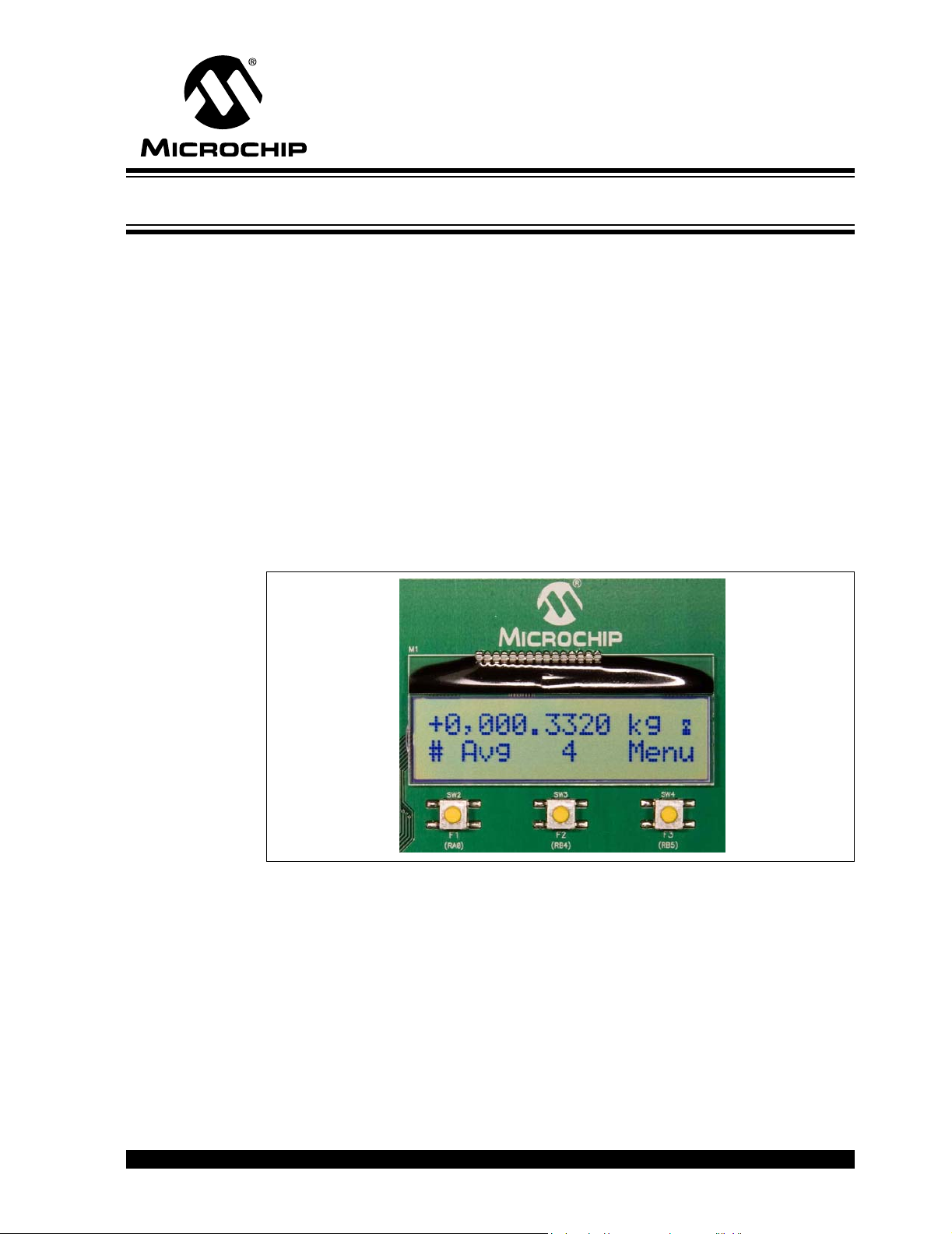
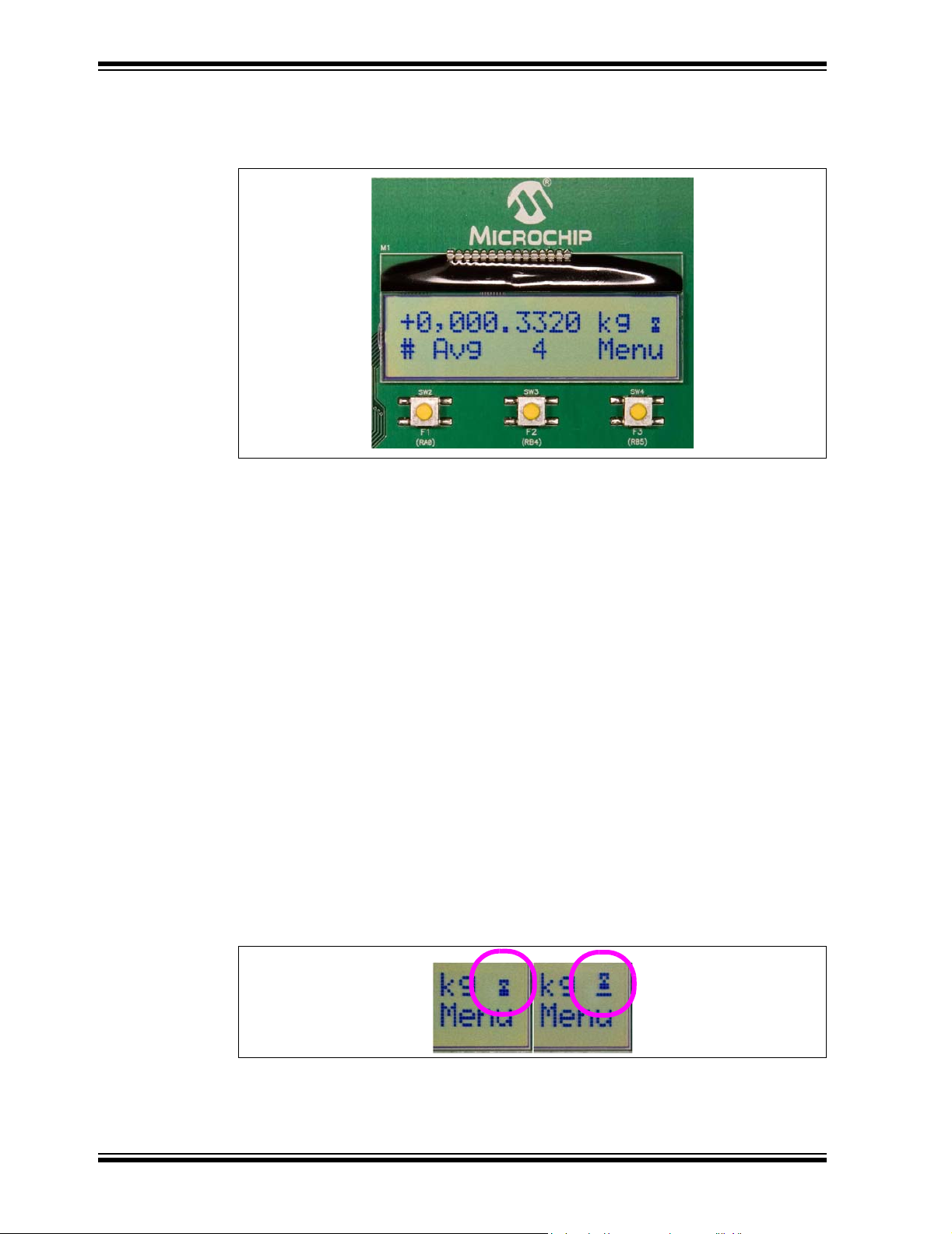
Figure 1-1 shows the LCD display output in kg of a high resolution system.
.
FIGURE 1-1: MCP355X Sensor Application Developer’s Board LCD showing
weigh scale output in kilograms.
Reference Design Features:
• Signal Conditioning Circuit Selection and Gain Selection
• Voltage Reference Selection
•PICmicro
• Preprogrammed LCD firmware for ADC Output in g, kg or system code
• DataView USB connection for easy PC evaluation of system error
• High Resolution System Board Design
© 2006 Microchip Technology Inc. DS51609A-page 5
®
microcontroller sockets and LCD for firmware development on-board
Page 10

MCP355X Sensor Application Developer’s Board User’s Guide
1.3 WHAT THE MCP355X SENSOR APPLICATION DEVELOPER’S BOARD KIT INCLUDES
This MCP355X Sensor Application Developer’s Board Kit includes:
• The MCP355X Sensor Application Developer’s Board, 102-00090
• MCP355X Sensor Application Developer’s Board User’s Guide (DS-51609)
• MCP3550/1/3 Data Sheet, “Low-Power Single Channel 22-Bit Delta Sigma ADCs”
(DS21950)
• AN1030, “Weigh Scale Applications for the MCP3551” (DS01030)
DS51609A-page 6 © 2006 Microchip Technology Inc.
Page 11
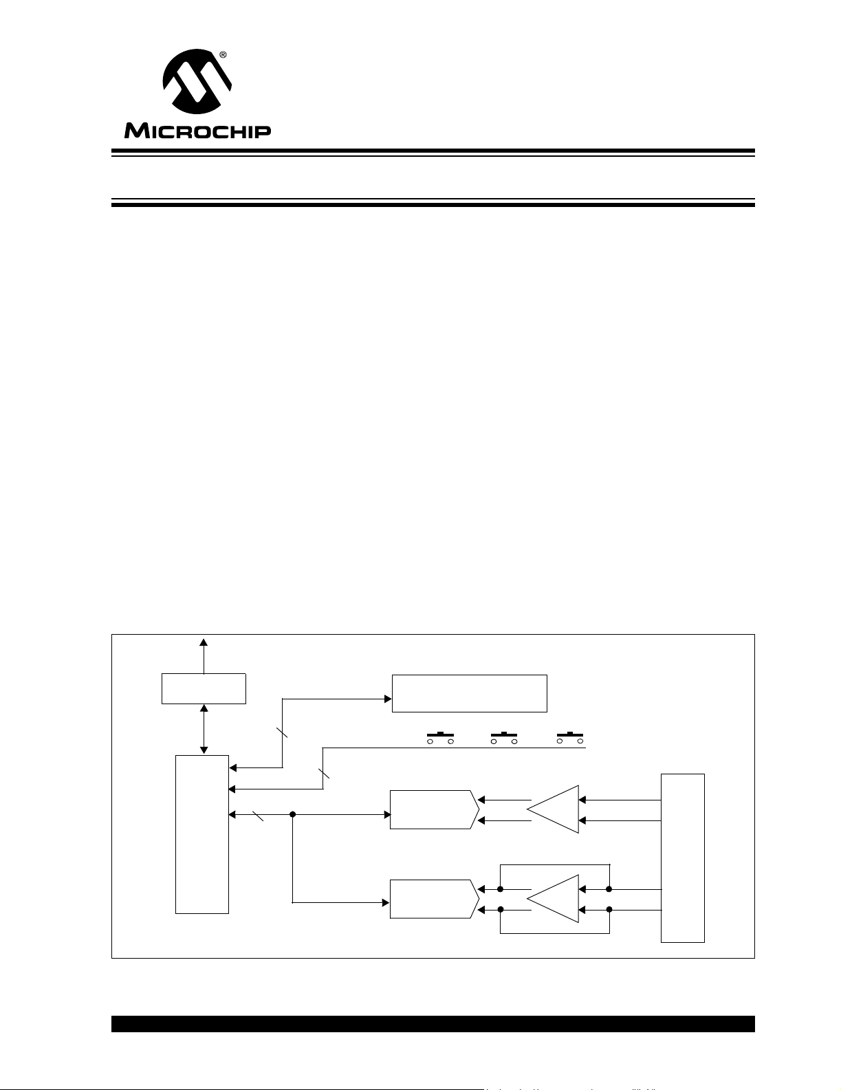
2.1 OVERVIEW
The MCP355X Sensor Application Developer’s Board’s purpose is to ease development of small signal sensor MCP355X applications such as weigh scales. There are
two circuits, or channels, to allow for comparison of different approaches to signal
conditioning circuits. The first channel is a low-cost, low-power signal conditioning
circuit that uses Microchip’s MCP6XX amplifiers. This circuit is intended to be a
reference design for low power, low cost MCP355X applications requiring intermediate
ranges of signal gain.
The second channel uses a precision amplifier with high gain. It is intended to be a
reference design for MCP355X circuits that can require higher resolution.
The board has jumper connections and screw terminals to connect external sensors
such as load cells or RTD temperature sensors. The board easily accomodates both
4-wire and 6-wire load cells sensor connections.
The system includes two PICmicro MCUs for firmware development and data analysis
through either an LCD display or graphically on a PC using a USB connection. A
PIC16F877 communicates with the two MCP355X channels, push-buttons and LCD
display.
For data analysis on the PC the USB PIC18F4550 is used. This device collects the
post processed PIC16F877 data and passes it via USB to the PC for display on
DataView software.
MCP355X SENSOR APPLICATION
DEVELOPER’S BOARD USER’S GUIDE
Chapter 2. Hardware Description
USB to PC running DataView
PIC18F4550
C
2
I
PIC16F877
FIGURE 2-1: MCP355X Sensor Application Developer’s Board Functional Block Diagram and
Results.
© 2006 Microchip Technology Inc. DS51609A-page 7
8
3
MCP3551 ΔΣ
4
SPI
MCP3551 ΔΣ
LCD Display
Push Button Control Switches
ADC
CHANNEL 1
ADC
CHANNEL 2
GAIN
GAIN
Sensor Input Connections
Page 12
MCP355X Sensor Application Developer’s Board User’s Guide
The following table shows example noise results of the two different channels.
TABLE 2-1: MCP355X SENSOR APPLICATION DEVELOPER’S BOARD CHANNEL
PERFORMANCE EXAMPLE RESULTS (NOTE 1)
Channel
Effective Number of Bits
(ENOB)
“Noise-free” ENOB
“Noise-free
Resolution”
Channel 1 15.8 13.1 8,800:1
Channel 2 18.8 16.1 70,000:1
Direct Connection (No Gain) 13 10.4 1,350:1
Note 1: Higher resolution systems are possible with averaging and other design approaches, table only serves as
an example. Sensor used for these results was a 200 kg external load cell. Amplifier used in Channel 1
was MCP617 device. Amplifier used in Channel 2 was CS3002. All results using MCP3551 A/D Converter.
2.2 SENSOR INPUT CONNECTIONS
There are three connectors located on the right hand side of the board for external
sensor input. The first is a standard DB9 connector that goes to a dual row 10-pin
header. Jumper wires must be used to connect the output of the header to the 12-pin
dual row headers going into either of the differential gain circuits described below.
In addition, there are two 3-terminal screw connectors, AUX1 and AUX2. These
connectors go directly into the right hand side of the 40-pin dual row connector P8.
Note: Connector P6 is the input for channel 1, and P7 is the input for channel 2.
Depending on which sensor inputs (AUX1, AUX2, or the DB9 connector) are
used to connect the external sensor to either channel, jumper wires must be
connected to bring the input into either P6 or P7.
P6
-SENSE
-IN
-OUT
+OUT
+IN
TO CHANNEL 1
P7
TO CHANNEL 2
Analog Input Headers To Signal
Conditioning Circuits
+SENSE
-SENSE
-IN
-OUT
+OUT
+IN
+SENSE
JUMPER WIRES
(NOT INCLUDED)
FIGURE 2-2: Sensor Input Connections.
5
9
4
8
3
7
2
P3
P9
P10
Headers Supplied For External
Sensor Connection
6
1
J4
DS51609A-page 8 © 2006 Microchip Technology Inc.
Page 13
Hardware Description
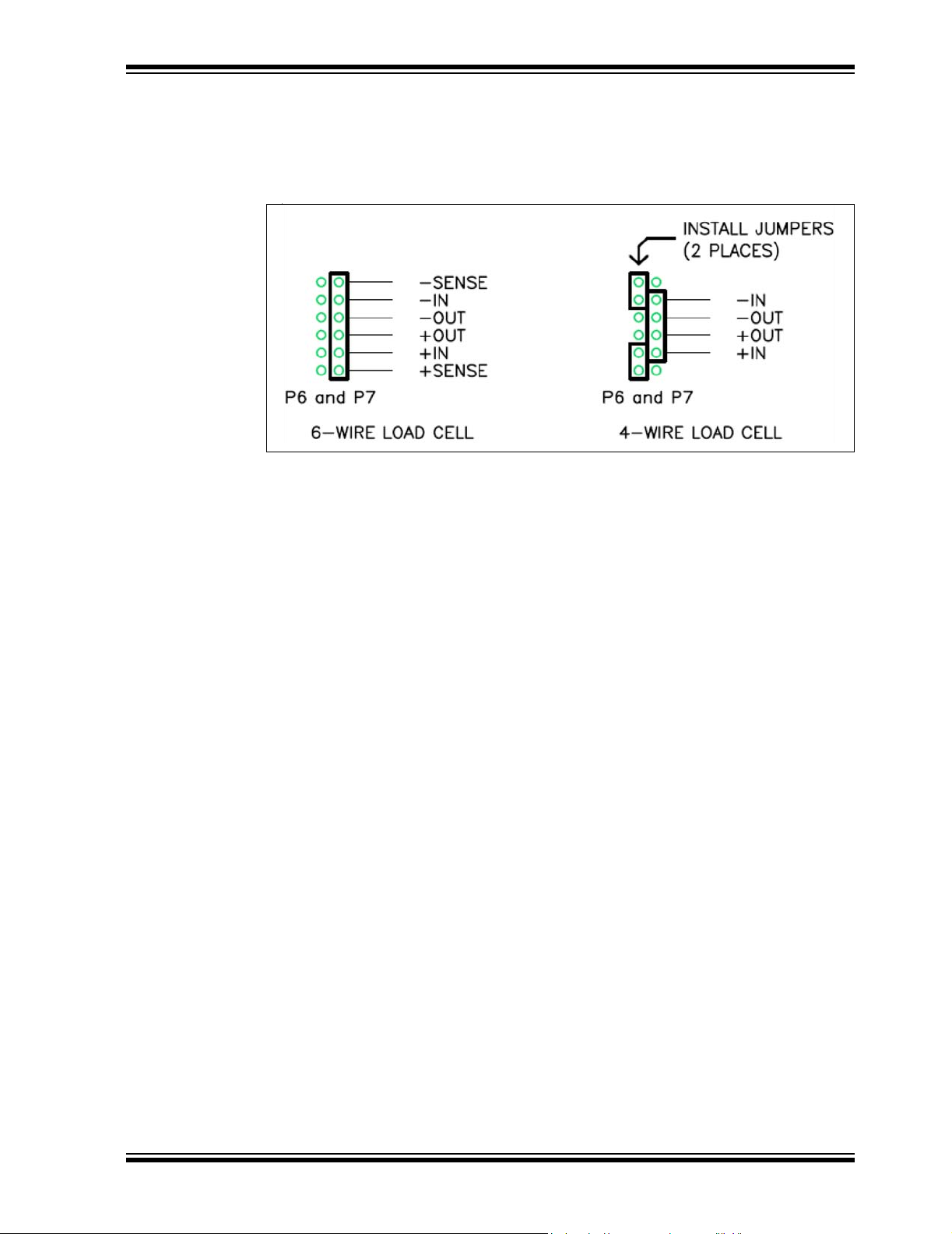
2.2.1 6-Wire and 4-Wire Load Cell Connections
P6 and P7 can be used to easily connect either 4 or 6-wire external load cell sensors.
Figure 2-3 describes how jumpers can be used to short the “In” and “Sense” inputs for
4-wire load cell connections.
FIGURE 2-3: 6-Wire and 4-Wire Load Cell connections on P6 and P7.
The MCP355X Sensor Application Developer’s Board comes with 2 “Bridge Simulator”
Boards that can be used in place of external sensors during system development.
These boards are plugged directly into P6 and P7, see Section 2.5 “Bridge Simulator
Boards” for more information.
2.3 CHANNEL 1 - LOW-COST DIFFERENTIAL GAIN CIRCUIT USING MCP6XX AMPLIFIER
Channel 1 contains a differential gain circuit using a dual amplifier PDIP socket
populated with Microchip’s MCP617 amplifier with two analog switches for offset
cancellation. The goal of the circuit is to allow for the use of an operational amplifier
with higher offset drift (which will generally mean a lower cost amplifier). The MCP617
is populated and configured to provide a differential gain of 21.
The board comes populated with R
chosen such that the voltage noise at the output of the amplifier will be approximately
10 µV
using the MCP617 amplifier will not provide any additional improvement to the system.
Application note AN1030 details the operation of this circuit and also includes data and
test results using a variety of external sensors.
, substantially above the 2.5 µV RMS noise of the MCP3551. Higher gains
RMS
=100Ω and RF = 1.0 kΩ. The gain of 21 was
G
© 2006 Microchip Technology Inc. DS51609A-page 9
Page 14

MCP355X Sensor Application Developer’s Board User’s Guide
U7
Analog Switch
MCP6XX Socket U9
+
SPI
V
REF
MCP3551
V
SS
U5
-
V
IN-
R
F
V
IN+
-
+
Analog Switch
R
G
P6
-SENSE
-IN
-OUT
+OUT
+IN
+SENSE
Switch Control From PIC16F877
U8
FIGURE 2-4: Channel 1 Differential Gain Circuit with analog switch offset
cancellation.
2.3.1 Channel 1 Analog Switches and Offset Drift Cancellation
The analog switches are used with the amplifier to swap the sources driving the load
cell, effectively cancelling any offset or offset drift. One conversion is performed with
the load cell driven “normally” and a second while it is driven in an “inverted”
configuration. The result of the second conversion is inverted and added to the result
from the first and an average of the two is computed (computing the average is a simple
shift operation for the microcontroller). This technique effectively cancels the offset of
the amplifiers as well as the ADC. An offset residue will exist if the any of the offsets
change between conversions. This is unlikely to happen unless the temperature
changes rapidly after the first conversion. The offset of the sensor is not affected by this
technique.
The firmware included with this developer’s board performs this process when
“Channel 1” is selected using the push button switches.
This process is described here:
1. Stop the output drive by configuring the outputs of the PICmicro MCU that drive
the load cell as low.
2. Control the analog switches and switch the ground of the MCP3551 to the
“bottom” of the load cell and the reference of the MCP3551 to the “top” of the load
cell.
3. Start the output drive by configuring the output of the PICmicro MCU that drives
the “top” of the load cell as high.
4. Perform a conversion and save the result.
5. Stop the output drive by configuring both outputs of the PICmicro MCU that drive
the load cell as low.
6. Control the analog switches and switch the ground of the MCP3551 to the “top”
of the load cell and the reference of the MCP3551 to the “bottom” of the load cell.
7. Start the output drive by configuring the output of the PICmicro MCU that drives
the “bottom” of the load cell as high.
8. Perform a conversion, invert the result, add to the first conversion, divide by two,
and save the result as the actual reading.
DS51609A-page 10 © 2006 Microchip Technology Inc.
Page 15

Hardware Description
2.4 CHANNEL 2 - HIGH-PRECISION GAIN CIRCUIT
Channel 2 contains a differential gain circuit using a low noise amplifier from Cirrus
Logic, CS3002. The noise allows a differential amplifier gain of 103 V/V.
EQUATION 2-1:
G12
This was chosen so that the amplifier noise would be similar to that of the MCP3551
device, maximizing the resolution of the circuit. The board comes populated with
R
=100Ω and RF = 5.1 kΩ. Higher gains can be chosen, however in this case, the
G
gain was chosen to allow for headroom near the supply rails (+5V and ground) to
handle a large variety of sensors. For more information regarding gain selection and
circuit results, refer to application note AN1030, “Weigh Scale Applications for the
MCP3551”.
U6
MCP3551
V
V
V
JP2
IN-
IN+
REF
GAINDIRECTDIRECT+
GAIN+
VREF
RC7
VDD
〈〉+=
R
------R
F
G
CS3002
+
-
R
F
-
+
P7
-SENSE
-IN
R
G
-OUT
+OUT
+IN
+SENSE
FIGURE 2-5: High Gain Circuit Using CS3002.
2.4.1 Channel 2 - Voltage Reference Selection
There are three options to select voltage reference for the MCP355X device for
channel 2. This is accomplished using the 14-pin dual row header JP2. There are three
options for voltage reference evaluation on the bottom of this header.
•V
REF
• PICmicro port pin RC6-7
•V
DD
The first selection uses the stand-alone voltage reference circuit included on the board,
populated with the low noise reference LM4140 from National Semiconductor
Corporation.The second selection allows for evaluation of using the PICmicro port pins
to supply the voltage reference for the circuit. The board uses two pins of the PICmicro
microcontroller for increased drive, RC6 and RC7 of the PIC16F877. The third
selection, V
, will supply the V
DD
directly from the output of JP1, which selects the
REF
power supply for the board.
© 2006 Microchip Technology Inc. DS51609A-page 11
®
Page 16

MCP355X Sensor Application Developer’s Board User’s Guide
2.4.2 Channel 2 - Direct-Connect Applications (No Amplifier or Gain)
Channel 2 can also be used to evaluate the MCP355X in a direct-connect sensor
configuration. This is accomplished using the 14-pin dual row header JP2. Changing
the headers to DIRECT+ and DIRECT- will take the signal present on the channel input
header (P7) directly into the MCP355X. Figure 2-6 represents this circuit configuration
using channel 2.
R
1
C
1
V
IN
VIN-
FIGURE 2-6: A Direct-connect Weigh Scale.
VDDV
+
MCP3551
V
REF
SS
2.5 BRIDGE SIMULATOR BOARDS
There are two small boards included with the MCP355X Sensor Application
Developer’s Board. These boards represent a simulation of an external wheatstone
bridge that is either at zero-scale or full-scale. These boards come populated with
resistors that have a temperature drift specification of 10 ppm/C. For the best bridge
simulation, it is recommended that the bridges be populated with very low drift resistors
with a tempco value of 0.1 ppm/C. Typical load cell bridges will exhibit this output
temperature drift. These boards can be plugged in to either P6 or P7 to assist in
eliminating any error associated with an external sensor. Figure 2-7 represents the
bridge simulator boards and how they should be connected to the MCP355X Sensor
Application Developer’s Board. Refer to Appendix A. “Schematic and Layouts” for
complete schematic.
P6 (OR P7)
-SENSE
-IN
-OUT
+OUT
+IN
+SENSE
Bridge Simulator Boards
FIGURE 2-7: Bridge Simulator Boards.
DS51609A-page 12 © 2006 Microchip Technology Inc.
Page 17

DEVELOPER’S BOARD USER’S GUIDE
Chapter 3. Firmware Description
3.1 FIRMWARE OVERVIEW
The MCP355X Sensor Application Developer’s Board contains two PICmicro MCUs,
the PIC18F4550, which is solely used to send ADC data to DataView on the PC and
the PIC16F877 which interfaces to the LCD display. Both controllers come programmed with dedicated firmware that is described in this chapter.
3.2 PIC16F877
This device comes programmed with LCD firmware to ease weigh scale or other
system design. The three push buttons F1, F2, and F3 control both the MCP3551
sampling and LCD output through the PIC16F877.
3.2.1 LCD Numerical Output Display
This display will change depending on the units selected and the values that are loaded
into the zero calibrate, full-scale calibrate, and full-scale value registers. To show raw
ADC output, the unit menu is used to select A/D units. When grams (g), or kilograms
(kg) is selected, Equation 3-1 represents the algorithm and formula applied to yield an
output on the LCD display.
MCP355X SENSOR APPLICATION
EQUATION 3-1:
ADC
⎛⎞
Output
Where:
ADC
VAL
ZERO
CAL
FS
CAL
DI SPLAY_FS_VAL = 1, 2, 5, 10, 20, 50, 100, 200, or 500 (value selected
Note: The ZERO
disabled. See Section 3.2.2.1 “Zero calibrate” for complete
description
----------------------------------------------------
=
⎝⎠
= The most recent value from the ADC after averaging.
= The most recent ADC
is pressed.
= The most recent (ADC
calibrate full-scale switch is pressed.
using push button switches.)
See Section 3.2.2.5 “Full-Scale Value Selection”
subtraction to remove zero offset can be enabled or
CAL
VAL
FS
ZERO
–
CAL
CAL
DISPLAY_FS_VAL
×
when the calibrate zero switch
VAL
VAL
- ZERO
) when the
CAL
© 2006 Microchip Technology Inc. DS51609A-page 13
Page 18
MCP355X Sensor Application Developer’s Board User’s Guide
3.2.2 Controlling the LCD Menu
The right most button F3 is the menu control button.
.
FIGURE 3-1: LCD showing the Averaging Menu. Also shown are the F1, F2
and F3 buttons.
Pressing this button will cycle through the menu options and change the functionality
of the other two buttons, F1 and F2. The LCD text above the buttons describes the
functionality for the different menus.
Here are the LCD menus that can be selected using the F3 button:
• Zero Calibrate - Enable/Disable/Hold
• Channel Select
•Units
• Averaging
• Full-Scale Value Selection
• Full-Scale Calibration
There are four different menu options that will be described in individual sections.
3.2.2.1 ZERO CALIBRATE
When in this menu, the first button becomes the ZERO button. When this button is
selected, the most recent ADC value after averaging will be loaded into the ZERO
register.
Zero calibration is also enabled or disabled by pressing the ZERO button. This is
indicated by a change of the spinning character on the far top-right of the display, (i.e.:
a LINE is inserted under the spinning character when zero calibration is turned ON.)
When enabled, ZERO
is subtracted as per Equation 3-1. Refer to Figure 3-2.
CAL
CAL
FIGURE 3-2: These two icons show the presence of the zero offset
substraction in the calculation. The icon on the right has a bar underneath that
represents when zero subtraction is enabled.
DS51609A-page 14 © 2006 Microchip Technology Inc.
Page 19

Firmware Description
In disabled mode, ZERO
direct ADC value (units = ADU), the output is simply the decimal representation of
ADC
displayed.
Pressing the HOLD button freezes the LCD display to allow for viewing in fast sampling
modes (less averaging). Pressing the HOLD button again will resume normal
operation.
3.2.2.2 CHANNEL SELECT
In this menu, the user has control over which channel is being sampled. There are four
options. Pressing either F1 or F2 cycles through these options:
. If zero calibrate is enabled, then ZERO
VAL
is not subtracted per Equation 3-1. When displaying the
CAL
is subtracted before the value is
CAL
Channel 1 Normal
In this mode, the PIC16F877 samples the MCP3551 on channel 1. The LCD text above
F2 will display “1N”. In the normal mode, the analog switches on this channel are set
to the “positive” polarity. Refer to Chapter 2. “Hardware Description” for more
description on the analog switch sampling.
Channel 1 Inverted
In this mode, the analog switches set to reverse polarity, and the inverted ADC sample
is displayed on the LCD display. The LCD text above F2 will display “1I”. Refer to
Chapter 2. “Hardware Description” for more description on the analog switch
sampling.
Channel 1 Switched
In this mode, the PIC16F877 is switching back and forth between positive and reverse
polarity and the averaged value is displayed on the LCD display. The LCD text above
F2 will display “1S”. Refer to Chapter 2. “Hardware Description” for more description
on the analog switch sampling.
Channel 2
In this mode, the PIC16F877 is sampling channel 2. This channel is the high gain circuit
using amplifier CS3002. The resulting code is displayed on the LCD display.
3.2.2.3 UNITS
There are three units: A/D Units (ADU), grams (g), or kilograms (kg). When in this
menu, pressing either F1 or F2 will change the text to the right of the numerical output
to the proper unit and also display the appropriate representation of the A/D sample.
3.2.2.4 AVERAGING
In the averaging menu, the user can select how many samples are collected before the
value is applied to the LCD output. This averaging applies all sampling situations, i.e.
when calibrating zero, full scale, or displaying the output after calibration. The user can
select between 1 (no averaging), 2, 4, 8, or 16 averages. The output noise of the
system will be reduced by the square root of the number of averages per the equation
below.
EQUATION 3-2:
MCP3551 Output Noise
Where:
N = the number of conversions
© 2006 Microchip Technology Inc. DS51609A-page 15
2.5 µV RMS
-----------------------------=
N
Page 20

MCP355X Sensor Application Developer’s Board User’s Guide
Note: If the channel mode “Channel 1 Switching” is selected, the averaging will
actually be twice due to the positive and reverse polarity switched samples
being collected.
3.2.2.5 FULL-SCALE VALUE SELECTION
This menu options loads the DISPLAY_FS_VAL register. This is to allow for proper LCD
display during system design. For example, if a system is being designed that uses
“100 grams” as the full-scale calibration weight, this menu is used to set the value “100”
into the DISPLAY_FS_VAL register. The full-scale value options are 1, 2, 5, 10, 20, 50,
100, 200, or 500.
Note: When displaying the value on the LCD display, the decimal point does not
move. This is to relax the LCD activity and keep the decimal point (and all
digits) from constantly switching location when the LCD output is
calculated.
3.2.2.6 FULL-SCALE CALIBRATION
When in this menu, the second button becomes the calibrate full-scale button, labeled
OK. When this button is selected, the most recent ADC value, after averaging, will be
loaded into the FS
CAL
register.
3.3 PIC18F4550
This device acts as I2C slave and passes the PIC16F877 output data from either
channel 1 or channel 2 to the DataView on the PC. All averaging and channel 1
switching that is performed by the PIC16F877 occurs before the data is passed to the
PIC18F4550 and PC.
Note: The PIC18F4550 passes data to DataView on the PC coming from the
PIC16F877. This allows a system developer to write PIC16F877 firmware
that averages or otherwise post processes ADC data and then use the PC
to view this post processed data, see section below. Refer to Figure 2-1 for
Data Flow.
DS51609A-page 16 © 2006 Microchip Technology Inc.
Page 21

4.1 OVERVIEW
DataView is a graphical data analysis tool that interfaces to many of Microchip’s
stand-alone A/D converter demonstration or evaluation boards via USB interface. Each
installation of Dataview is specific to the A/D converter and will contain one or more of
the following graphical output windows:
• Scope Plot
• Histogram
• Auxiliary Data
MCP355X SENSOR APPLICATION
DEVELOPER’S BOARD USER’S GUIDE
Chapter 4. DataView
Note: IMPORTANT! For the MCP355X Sensor Application Developer’s Board,
the USB microcontroller (PIC18F4550) is collecting post-processed data
from the PIC16F877. By pressing the push button switches on the
reference design and changing the processing that occurs on the
PIC16F877, the data shown on DataView is also changed.
4.2 SCOPE PLOT WINDOW
The scope plot window graphs the A/D output as a function of sample or time. Each
consecutive sample is added to the right of the data set and when the sample size is
full, the scope plot will scroll to the left. The y-axis is displayed as the ADC code and
the x-axis is given as sample number. The sample size can be changed in the
configuration window.
FIGURE 4-1: Scope Plot Window.
© 2006 Microchip Technology Inc. DS51609A-page 17
Page 22

MCP355X Sensor Application Developer’s Board User’s Guide
4.3 NOISE HISTOGRAM WINDOW
The noise histogram window displays the ADC output in histogram form, building the
number of occurrences in each bin with each consecutive sample. The difference
between each bin from the mean in units of LSB is given as the y-axis. The sample size
can be changed in the configuration window.
FIGURE 4-2: Noise Histogram Window.
4.4 AUXILIARY DATA WINDOW
The auxiliary data window shows calculated data based on the current sample size.
The mean of the sample set is given in both LSB and PPM. The standard deviation or
RMS output noise is given in units PPM. The overflow bits of the MCP3551 are also
monitored and the overflow bits are also given for both overflow high and overflow low
situations.
FIGURE 4-3: Noise Histogram Window.
DS51609A-page 18 © 2006 Microchip Technology Inc.
Page 23

4.5 CONFIGURING DATAVIEW
The sample size and polling interval of the USB interface can be changed to
accommodate customized firmware on the PICmicro microcontroller side. The units of
millisecond, seconds, minute, hour or day can be used to change the functionality of
the system. This allows the device to be used as a “Data Logger”. Note that if the polling
interval is shorter than the sampling rate on the hardware size, duplicate data will be
included in the sample set.
DataView
FIGURE 4-4: Configuration Window.
© 2006 Microchip Technology Inc. DS51609A-page 19
Page 24

MCP355X Sensor Application Developer’s Board User’s Guide
NOTES:
DS51609A-page 20 © 2006 Microchip Technology Inc.
Page 25

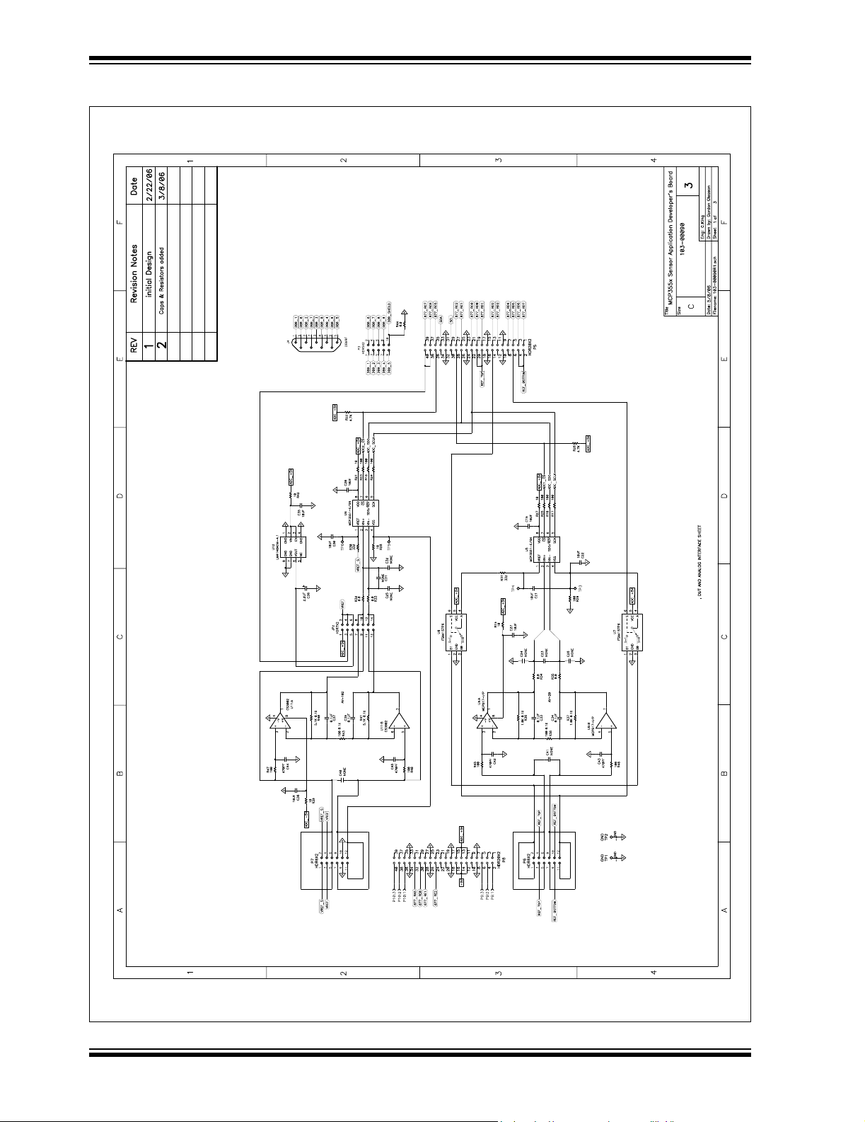
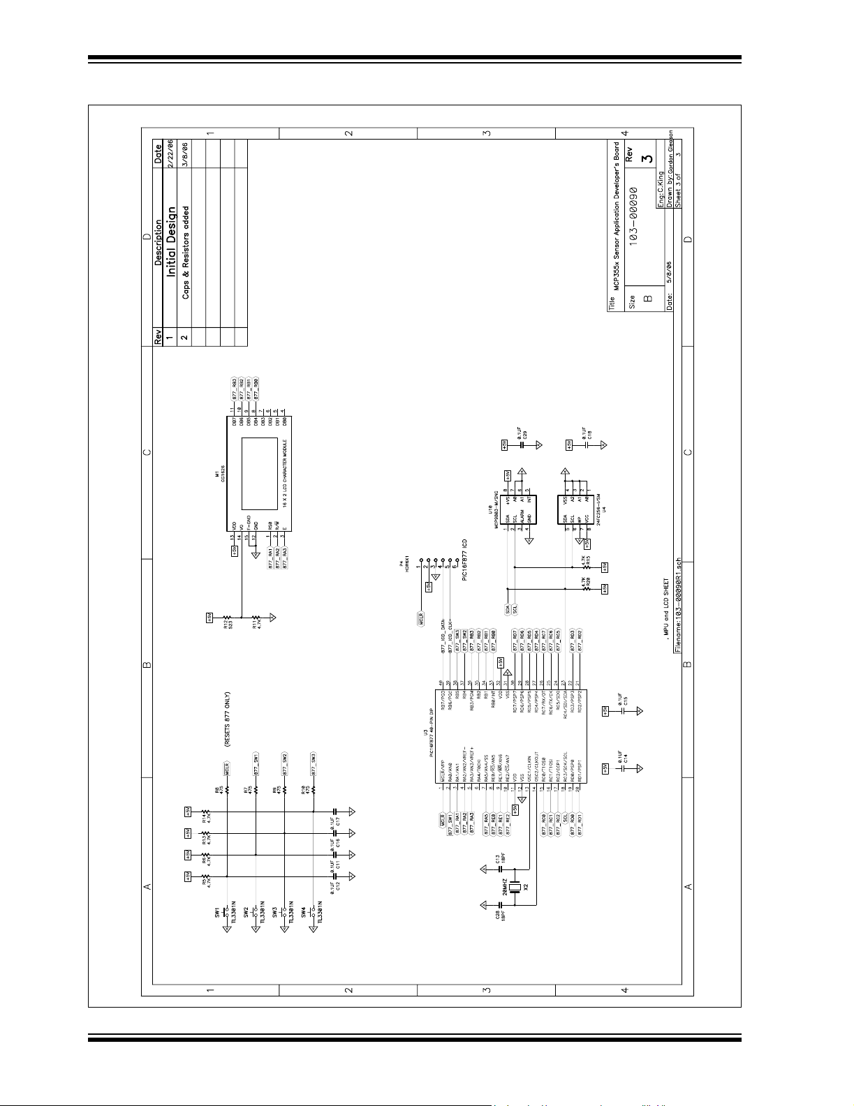
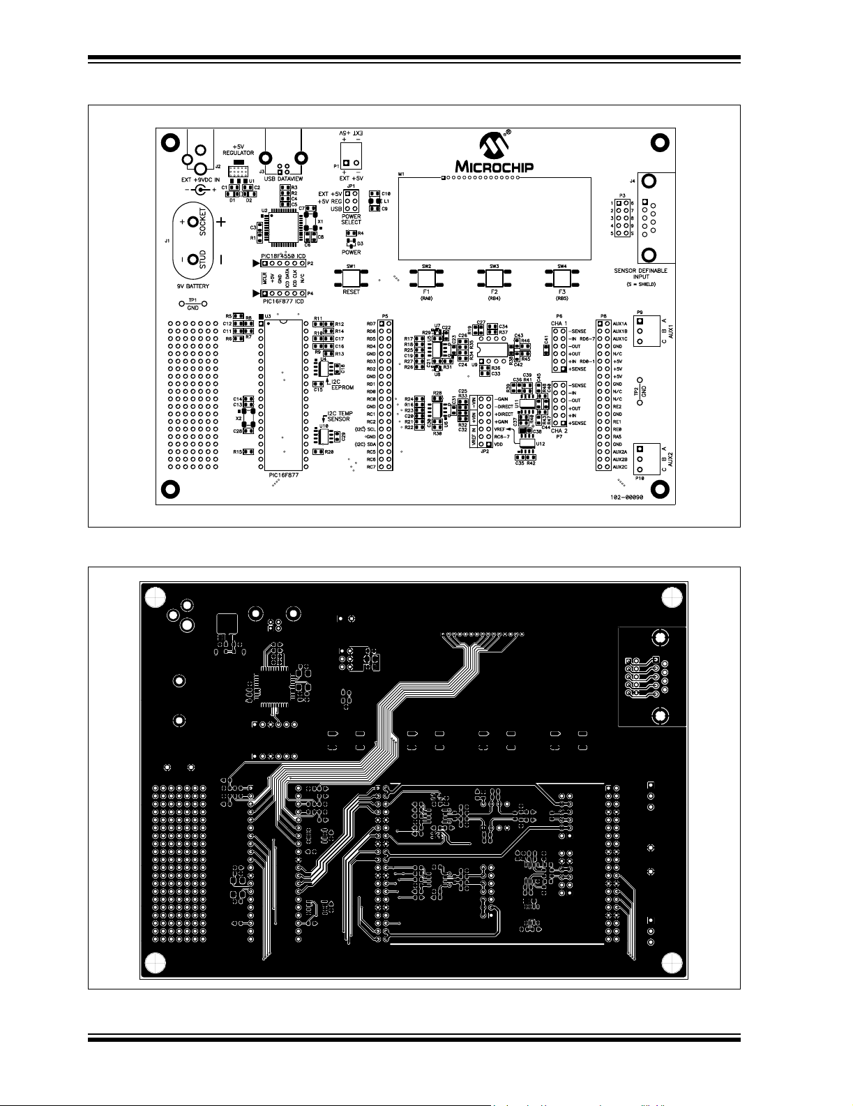
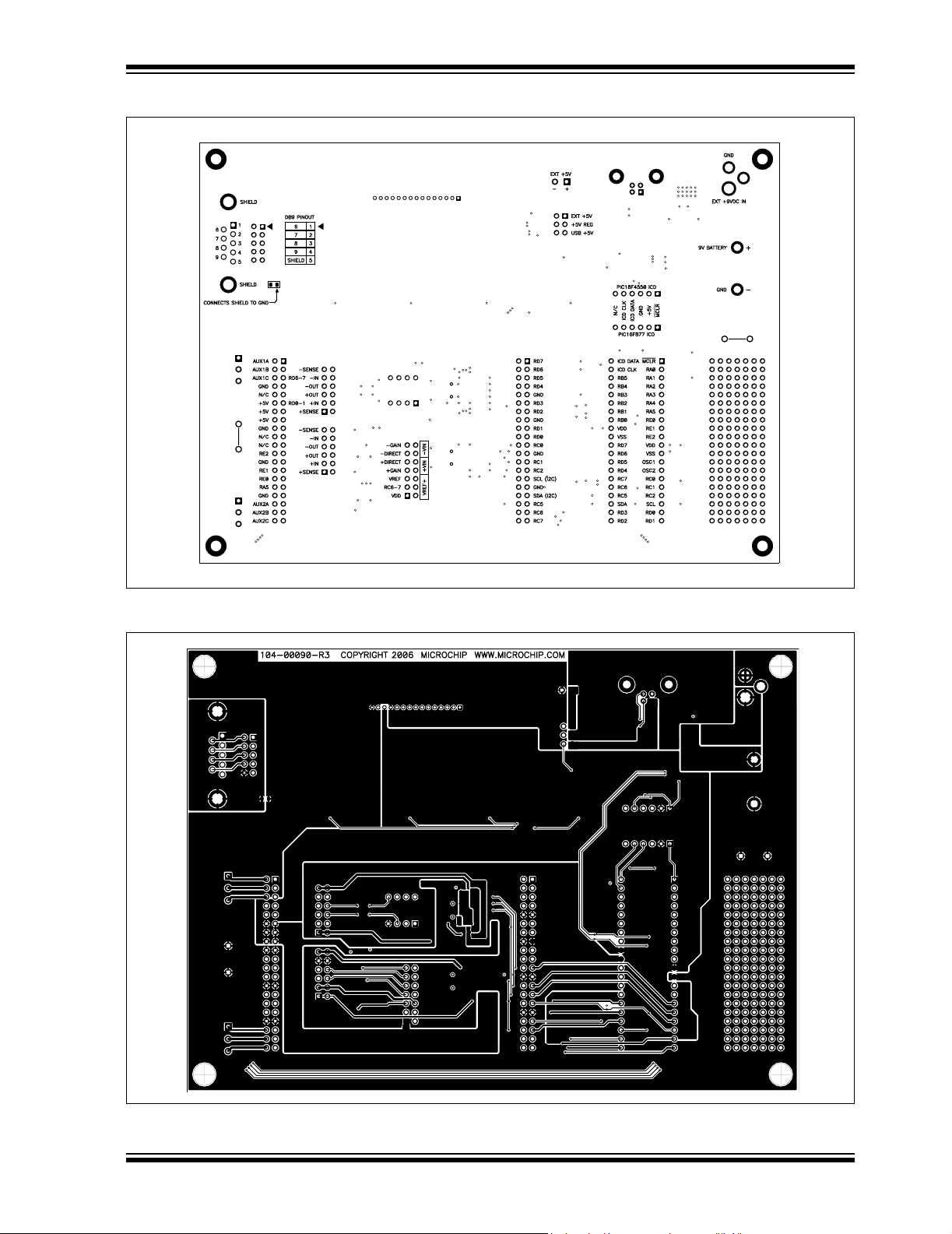
Appendix A. Schematic and Layouts
A.1 INTRODUCTION
This appendix contains the following schematics and layouts for the MCP355X Sensor
Application Developer’s Board:
• Board Schematic, Pages 1 thru 3
• Board Schematic - Bridge Simulator
• Board - Top Layer and Silk Screen
• Board - Top Layer
• Board - Bottom Layer and Silk Screen
• Board - Bottom Layer
• Board - Bridge Simulator Layout
MCP355X SENSOR APPLICATION
DEVELOPER’S BOARD USER’S GUIDE
© 2006 Microchip Technology Inc. DS51609A-page 21
Page 26
MCP355X Sensor Application Developer’s Board User’s Guide
A.2 SCHEMATIC - PAGE 1
M
DS51609A-page 22 © 2006 Microchip Technology Inc.
Page 27

A.3 SCHEMATIC - PAGE 2
Schematic and Layouts
M
© 2006 Microchip Technology Inc. DS51609A-page 23
Page 28
MCP355X Sensor Application Developer’s Board User’s Guide
A.4 SCHEMATIC - PAGE 3
M
DS51609A-page 24 © 2006 Microchip Technology Inc.
Page 29
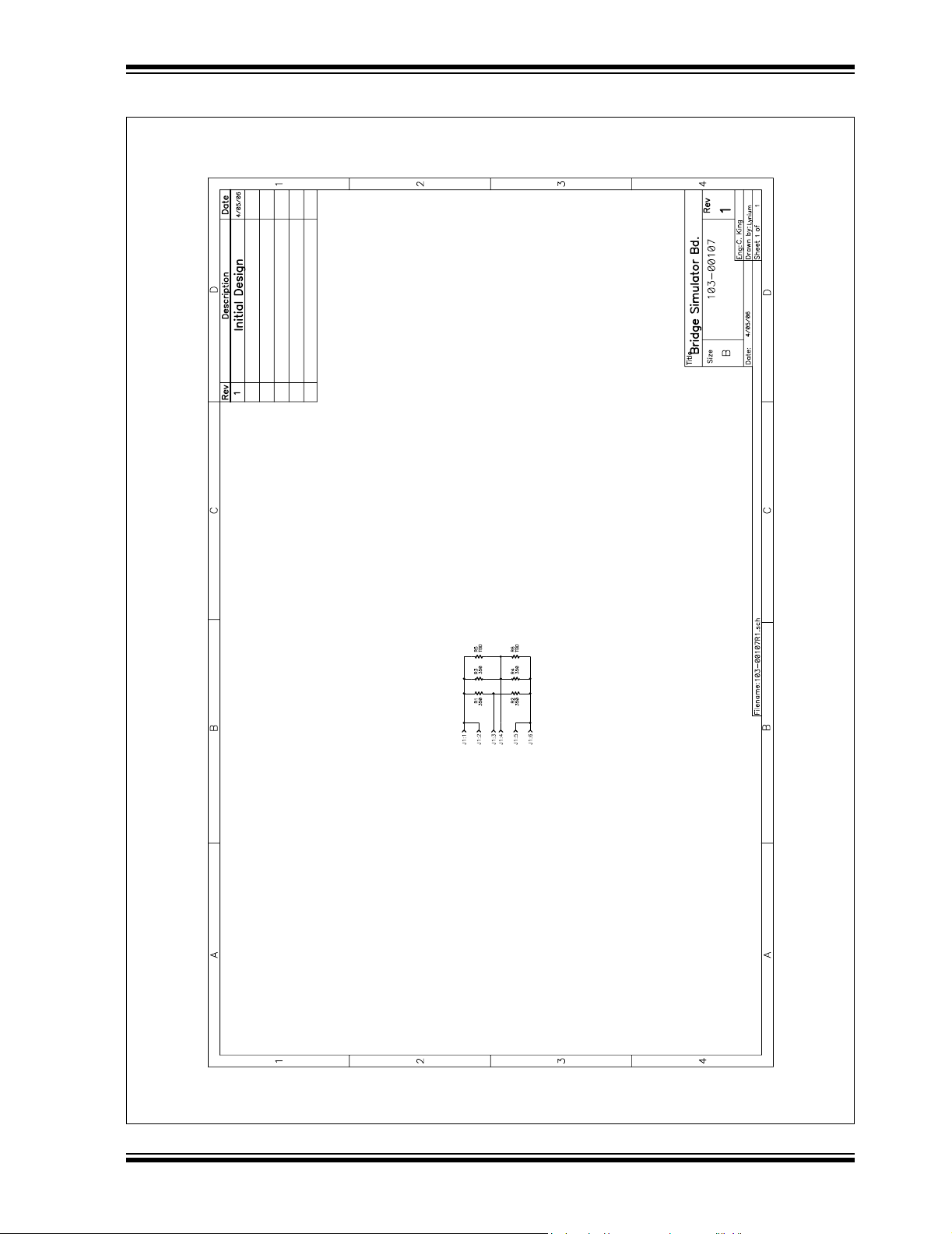
A.5 SCHEMATIC - BRIDGE SIMULATOR
Schematic and Layouts
M
© 2006 Microchip Technology Inc. DS51609A-page 25
Page 30
MCP355X Sensor Application Developer’s Board User’s Guide
A.6 BOARD LAYOUT - TOP LAYER AND SILK SCREEN
MCP355x SENSOR APPLICATION DEVELOPER'S BOARD
A.7 BOARD LAYOUT - TOP LAYER
DS51609A-page 26 © 2006 Microchip Technology Inc.
Page 31
Schematic and Layouts
A.8 BOARD LAYOUT - BOTTOM LAYER AND SILK SCREEN
A.9 BOARD LAYOUT - BOTTOM LAYER
© 2006 Microchip Technology Inc. DS51609A-page 27
Page 32

MCP355X Sensor Application Developer’s Board User’s Guide
A.10 BOARD LAYOUT - BRIDGE SIMULATOR
DS51609A-page 28 © 2006 Microchip Technology Inc.
Page 33

MCP355X SENSOR APPLICATION
DEVELOPER’S BOARD USER’S GUIDE
Appendix B. Bill Of Materials (BOM)
TABLE B-1: BILL OF MATERIALS (BOM)
Qty
17 C1, C3, C4, C5,
11 C2, C9, C10,
4 C7, C8, C13,
8 C23, C24 C25,
1 C38 CAP TANTALUM 2.2UF 16V 10%
4 C42, C43, C44,
2 D1, D2 DIODE SCHOTTKY 20V 0.5A
1 D3 LED SMD Standard SOT-23 HI
4 EA Corner BUMPON HEMISPHERE .44X.20
1 J1 9V Battery PCB Mount Vert
1 J2 Power Jack ,08" RA PCB Switchcraft RAPC722X
1 J3 CONN USB RECEPT R/A TYPE B
1 J4 9 Pin Right Angle Female
1 JP1 CONN HEADER RT/A .100 6POS
1 JP2 CONN HDR 14PIN GOLD VERT
1 L1 Shielded 10uH Power Inductor
1 M1 16 X 2 LCD Character Display Fema CG1626-SGR1
1 P1 Conn header pins used W/TERM
1 P1 CONN TERM BLK PLUG 6A
Designator Description Manufacturer Part Number
C6, C11, C12,
C14, C15, C16,
C17, C18, C29,
C33, C34, C37,
C39
C19, C20, C21,
C22, C27, C30,
C35, C36
C28
C26, C31 C32,
C40, C41
C45
CAP .1UF 25V CERAMIC X7R
0805
CAP CER 10UF 6.3V X7R 0805 Murata Electronics
CAP CERAMIC 18PF 50V NP0
0805
DO NOT INSTALL — —
SMD 3216
CAP 470PF 50V CERM CHIP 0805
SMD
SOD123
EFF RED WTR CLR
BLACK
Connector Snap-on
4POS
Connector D-Sub
15AU
PCB
0805
BLK PLUG
3.5MM 2POS
Panasonic® - ECG ECJ-2VB1E104K
®
GRM21BR70J106KE76L
North America
Yageo® America CC0805JRNPO9BN180
EPCOS Inc B45196H3225K109
Panasonic - ECG ECJ-2VC1H471J
ON Semiconductor
Kingbright AM23EC-F
3M/ESM SJ-5003 (BLACK)
Keystone
Electronics
AMP
Electronics
Amphenol Canada 205A-09FGTBBC3
AMP/Tyco
Electronics
CW Industries CWN-350-14-0000
Coilcraft 0805PS-103KLB
Keystone Electronics 8724
Keystone Electronics 8722
®
/Tyco®
®
®
MBR0520LT1G
968
292304-1
87230-3
© 2006 Microchip Technology Inc. DS51609A-page 29
Page 34

MCP355X Sensor Application Developer’s Board User’s Guide
TABLE B-1: BILL OF MATERIALS (BOM) (CONTINUED)
Qty
2 P2, P4 6 X 1 Header 2.54mm on center 6
1 P3 5 X 2 Header 2.54mm on center 6
2 P5, P8 20 X 2 Header 2.54mm on center 6
2 P6, P7 6 X 2 Header 2.54mm on center 6
2 P9, P10 3.5mm Plugable 3-Position Screw
2 P9, P10 Conn header pins used W/TERM
1 PCB RoHS-compliant Bare PCB — 104-00090
10 R1, R5, R6,
2 R2, R3 RES 24.9 OHM 1/8W 1% 0805
3 R4, R30, R31 RES 332 OHM 1/8W 1% 0805 SMD Panasonic - ECG ERJ-6ENF3320V
4 R7, R8, R9,
1 R14 RES 887 OHM 1/8W 1% 0805 SMD Panasonic - ECG ERJ-6ENF8870V
11 R16, R17, R18,
6 R19, R21, R27,
4 R32, R33, R34,
2 R36, R37 1K Ohm 0.1% 0805 10ppm Thin
2 R38, R43 100 Ohm 0.1% 0805 10ppm Thin
2 R40, R41 5.1K Ohm 0.1% 0805 10ppm Thin
1 R44 DO NOT INSTALL — —
4 SW1 - SW4 SWITCH TACT 6MM SMD MOM
2 TP1, TP2 Wire Test Point 0.3" Length Nedco Electronics PJ-202-30
4 TP3, TP4 TP5,
1 U1 5.0V 3-Terminal 800mA Positive
1 U2 44-Pin, High-Performance,
1 U3 IC SOCKET STRAIGHT 40POS
Designator Description Manufacturer Part Number
Samtec TSW-106-07-G-S
mm/2.5mm
Samtec TSW-105-07-G-D
mm/2.5mm
Samtec TSW-120-07-G-D
mm/2.5mm
Samtec TSW-106-07-G-D
mm/2.5mm
Keystone Electronics 8723
Terminal Blocks
Keystone Electronics 8724
BLK PLUG
®
Yageo
America RC0805FR-074K7L
Panasonic - ECG ERJ-6ENF24R9V
Panasonic - ECG ERJ-3EKF10R0V
Susumu RG2012N-102-B-T1
Susumu RG2012N-101-B-T1
Susumu RG2012N-512-B-T1
Omron Electronics
Inc
National
Semiconductor
Microchip
Technology Inc.
Assmann Electronics
Inc
®
B3S-1002
LM1117-5.0
PIC18F4550-I/PT
A40-LC-TT-R
R11, R13, R14,
R15, R20, R22,
R26
R10, R12
R23, R24, R25,
R29, R45, R46,
R47, R48
R28, R39, R42
R35
TP6
4.7K 1% 0805 Thick Film Chip
Resistor
SMD
RES 475 OHM 1/8W 1% 0805 SMD Panasonic - ECG ERJ-6ENF4750V
RES 100 OHM 1/8W 1% 0805 SMD Panasonic - ECG ERJ-6ENF1000V
RES 10.0 OHM 1/10W 1% 0805
SMD
RES 0.0 OHM 1/8W 5% 0805 SMD Panasonic - ECG ERJ-6GEY0R00V
Film Chip Resistor
Film Chip Resistor
Film Chip Resistor
230GF
DO NOT INSTALL — —
Regulator SOT-223
Enhanced Flash, USB
Microcontroller
.600 TIN
DS51609A-page 30 © 2006 Microchip Technology Inc.
Page 35

Bill Of Materials (BOM)
TABLE B-1: BILL OF MATERIALS (BOM) (CONTINUED)
Qty
1 U3 40-Pin Enhanced Flash Microcon-
1 U4 256K I2C™ CMOS Serial EEPROM Microchip
2 U5, U6 22-Bit Delta Sigma ADC SO-8 Microchip
2 U7, U8 IC SWITCH ANALOG SPDT LV
1 U9 Dual Op-Amp DIP-8
1 U9 IC SOCKET STRAIGHT 8POS TIN Assmann Electronics
1 U10 I2C Temperature Sensor SO-8 Microchip
1 U11 Dual Op-Amp SO-8 Cirrus Logic CS3002-ISZ
1 U12 4.096V Voltage Reference SO-8 National Semicon-
2 X1, X2 20.000MHZ Crystal 10PF 5mm X
Designator Description Manufacturer Part Number
trollers
SC70-6
(Install in socket))
3.2mm SMD
Microchip
Technology Inc.
Technology Inc.
Technology Inc.
Fairchild
Semiconductor
Microchip
Technology Inc.
Inc
Technology Inc.
ductor
Abracon Corporation ABM3B-20.000MHZ-10-1-U-T
®
PIC16F877A-I/P
24FC256-I/SN
MCP3551-E/SN
FSA4157P6X_NL
MCP617-I/P
A08-LC-TT-R
MCP9803-M/SNG
LM4140ACM-4.1
© 2006 Microchip Technology Inc. DS51609A-page 31
Page 36

WORLDWIDE SALES AND SERVICE
AMERICAS
Corporate Office
2355 West Chandler Blvd.
Chandler, AZ 85224-6199
Tel: 480-792-7200
Fax: 480-792-7277
Technical Support:
http://support.microchip.com
Web Address:
www.microchip.com
Atlanta
Alpharetta, GA
Tel: 770-640-0034
Fax: 770-640-0307
Boston
Westborough, MA
Tel: 774-760-0087
Fax: 774-760-0088
Chicago
Itasca, IL
Tel: 630-285-0071
Fax: 630-285-0075
Dallas
Addison, TX
Tel: 972-818-7423
Fax: 972-818-2924
Detroit
Farmington Hills, MI
Tel: 248-538-2250
Fax: 248-538-2260
Kokomo
Kokomo, IN
Tel: 765-864-8360
Fax: 765-864-8387
Los Angeles
Mission Viejo, CA
Tel: 949-462-9523
Fax: 949-462-9608
San Jose
Mountain View, CA
Tel: 650-215-1444
Fax: 650-961-0286
Toronto
Mississauga, Ontario,
Canada
Tel: 905-673-0699
Fax: 905-673-6509
ASIA/PACIFIC
Australia - Sydney
Tel: 61-2-9868-6733
Fax: 61-2-9868-6755
China - Beijing
Tel: 86-10-8528-2100
Fax: 86-10-8528-2104
China - Chengdu
Tel: 86-28-8676-6200
Fax: 86-28-8676-6599
China - Fuzhou
Tel: 86-591-8750-3506
Fax: 86-591-8750-3521
China - Hong Kong SAR
Tel: 852-2401-1200
Fax: 852-2401-3431
China - Qingdao
Tel: 86-532-8502-7355
Fax: 86-532-8502-7205
China - Shanghai
Tel: 86-21-5407-5533
Fax: 86-21-5407-5066
China - Shenyang
Tel: 86-24-2334-2829
Fax: 86-24-2334-2393
China - Shenzhen
Tel: 86-755-8203-2660
Fax: 86-755-8203-1760
China - Shunde
Tel: 86-757-2839-5507
Fax: 86-757-2839-5571
China - Wuhan
Tel: 86-27-5980-5300
Fax: 86-27-5980-5118
China - Xian
Tel: 86-29-8833-7250
Fax: 86-29-8833-7256
ASIA/PACIFIC
India - Bangalore
Tel: 91-80-4182-8400
Fax: 91-80-4182-8422
India - New Delhi
Tel: 91-11-5160-8631
Fax: 91-11-5160-8632
India - Pune
Tel: 91-20-2566-1512
Fax: 91-20-2566-1513
Japan - Yokohama
Tel: 81-45-471- 6166
Fax: 81-45-471-6122
Korea - Gumi
Tel: 82-54-473-4301
Fax: 82-54-473-4302
Korea - Seoul
Tel: 82-2-554-7200
Fax: 82-2-558-5932 or
82-2-558-5934
Malaysia - Penang
Tel: 60-4-646-8870
Fax: 60-4-646-5086
Philippines - Manila
Tel: 63-2-634-9065
Fax: 63-2-634-9069
Singapore
Tel: 65-6334-8870
Fax: 65-6334-8850
Taiwan - Hsin Chu
Tel: 886-3-572-9526
Fax: 886-3-572-6459
Taiwan - Kaohsiung
Tel: 886-7-536-4818
Fax: 886-7-536-4803
Taiwan - Taipei
Tel: 886-2-2500-6610
Fax: 886-2-2508-0102
Thailand - Bangkok
Tel: 66-2-694-1351
Fax: 66-2-694-1350
EUROPE
Austria - Wels
Tel: 43-7242-2244-399
Fax: 43-7242-2244-393
Denmark - Copenhagen
Tel: 45-4450-2828
Fax: 45-4485-2829
France - Paris
Tel: 33-1-69-53-63-20
Fax: 33-1-69-30-90-79
Germany - Munich
Tel: 49-89-627-144-0
Fax: 49-89-627-144-44
Italy - Milan
Tel: 39-0331-742611
Fax: 39-0331-466781
Netherlands - Drunen
Tel: 31-416-690399
Fax: 31-416-690340
Spain - Madrid
Tel: 34-91-708-08-90
Fax: 34-91-708-08-91
UK - Wokingham
Tel: 44-118-921-5869
Fax: 44-118-921-5820
02/16/06
DS51609A-page 32 © 2006 Microchip Technology Inc.
 Loading...