

Page 1
MCP3422
Evaluation Board
for PICkit™ Serial
User’s Guide
© 2008 Microchip Technology Inc. DS51781A
Page 2
Note the following details of the code protection feature on Microchip devices:
• Microchip products meet the specification contained in their particular Microchip Data Sheet.
• Microchip believes that its family of products is one of the most secure families of its kind on the market today, when used in the
intended manner and under normal conditions.
• There are dishonest and possibly illegal methods used to breach the code protection feature. All of these methods, to our
knowledge, require using the Microchip products in a manner outside the operating specifications contained in Microchip’s Data
Sheets. Most likely, the person doing so is engaged in theft of intellectual property.
• Microchip is willing to work with the customer who is concerned about the integrity of their code.
• Neither Microchip nor any other semiconductor manufacturer can guarantee the security of their code. Code protection does not
mean that we are guaranteeing the product as “unbreakable.”
Code protection is constantly evolving. We at Microchip are committed to continuously improving the code protection features of our
products. Attempts to break Microchip’s code protection feature may be a violation of the Digital Millennium Copyright Act. If such acts
allow unauthorized access to your software or other copyrighted work, you may have a right to sue for relief under that Act.
Information contained in this publication regarding device
applications and the like is provided only for your convenience
and may be superseded by updates. It is your responsibility to
ensure that your application meets with your specifications.
MICROCHIP MAKES NO REPRESENTATIONS OR
WARRANTIES OF ANY KIND WHETHER EXPRESS OR
IMPLIED, WRITTEN OR ORAL, STATUTORY OR
OTHERWISE, RELATED TO THE INFORMATION,
INCLUDING BUT NOT LIMITED TO ITS CONDITION,
QUALITY, PERFORMANCE, MERCHANTABILITY OR
FITNESS FOR PURPOSE. Microchip disclaims all liability
arising from this information and its use. Use of Microchip
devices in life support and/or safety applications is entirely at
the buyer’s risk, and the buyer agrees to defend, indemnify and
hold harmless Microchip from any and all damages, claims,
suits, or expenses resulting from such use. No licenses are
conveyed, implicitly or otherwise, under any Microchip
intellectual property rights.
Trademarks
The Microchip name and logo, the Microchip logo, Accuron,
dsPIC, K
EELOQ, KEELOQ logo, MPLAB, PIC, PICmicro,
PICSTART, rfPIC, SmartShunt and UNI/O are registered
trademarks of Microchip Technology Incorporated in the
U.S.A. and other countries.
FilterLab, Linear Active Thermistor, MXDEV, MXLAB,
SEEVAL, SmartSensor and The Embedded Control Solutions
Company are registered trademarks of Microchip Technology
Incorporated in the U.S.A.
Analog-for-the-Digital Age, Application Maestro, CodeGuard,
dsPICDEM, dsPICDEM.net, dsPICworks, dsSPEAK, ECAN,
ECONOMONITOR, FanSense, In-Circuit Serial
Programming, ICSP, ICEPIC, Mindi, MiWi, MPASM, MPLAB
Certified logo, MPLIB, MPLINK, mTouch, PICkit, PICDEM,
PICDEM.net, PICtail, PIC
32
logo, PowerCal, PowerInfo,
PowerMate, PowerT ool, REAL ICE, rfLAB, Select Mode, Total
Endurance, WiperLock and ZENA are trademarks of
Microchip Technology Incorporated in the U.S.A. and other
countries.
SQTP is a service mark of Microchip Technology Incorporated
in the U.S.A.
All other trademarks mentioned herein are property of their
respective companies.
© 2008, Microchip Technology Incorporated, Printed in the
U.S.A., All Rights Reserved.
Printed on recycled paper.
Microchip received ISO/TS-16949:2002 certification for its worldwide
headquarters, design and wafer fabrication facilities in Chandler and
T empe, Arizona; Gresham, Oregon and design centers in California
and India. The Company’s quality system processes and procedures
are for its PIC
devices, Serial EEPROMs, microperipherals, nonvolatile memo ry and
analog products. In addition, Microchip’s quality system for the desig n
and manufacture of development systems is ISO 9001:2000 certified.
®
MCUs and dsPIC® DSCs, KEELOQ
®
code hopping
DS51781A-page ii © 2008 Microchip Technology Inc.
Page 3

MCP3422 EVALUATION BOARD FOR
PICkit™ SERIAL USER’S GUIDE
Table of Contents
Preface ...........................................................................................................................1
Introduction............................................................................................................1
Document Layout..................................................................................................1
Conventions Used in this Guide............................................................................2
Recommended Reading........................................................................................3
The Microchip Web Site........................................................................................ 3
Customer Support.................................................................................................3
Document Revision History...................................................................................3
Chapter 1. Quick Start Instructions
1.1 Introduction .....................................................................................................5
1.2 Description of the MCP3422 Evaluation Board ..............................................5
1.3 Getting Started with the PICkit Serial Analyzer .............................................. 6
Appendix A. Schematic and Layouts
A.1 Introduction ..................................................................................................21
A.2 Board Schematic ..........................................................................................22
A.3 Board – Top Layer ....................................................................................... 23
A.4 Board – Top Metal Layer .............................................................................24
A.5 Board – Bottom Layer .................................................................................25
Appendix B. Bill Of Materials (BOM)
Worldwide Sales and Service ....................................................................................28
© 2008 Microchip Technology Inc. DS51781A-page iii
Page 4

MCP3422 Evaluation Board for PICkit™ Serial User’s Guide
NOTES:
DS51781A-page iv © 2008 Microchip Technology Inc.
Page 5
MCP3422 EVALUATION BOARD FOR
PICkit™ SERIAL USER’S GUIDE
Preface
NOTICE TO CUSTOMERS
All documentation becomes dated, and this manual is no exception. Microchip tools and
documentation are constantly evolving to meet customer needs, so some actual dialogs
and/or tool descriptions may differ from those in this document. Please refer to our web site
(www.microchip.com) to obtain the latest documentation available.
Documents are identified with a “DS” number. This number is located on the bottom of each
page, in front of the page number . The numbering convention for the DS number is
“DSXXXXXA”, where “XXXXX” is the document number and “A” is the revision level of the
document.
For the most up-to-date information on development tools, see the MPLAB
Select the Help menu, and then Topics to open a list of available on-line help files.
®
IDE on-line help.
INTRODUCTION
This chapter contains general information that will be useful to know before using the
MCP3422 Evaluation Board. Items discussed in this chapter include:
• Document Layout
• Conventions Used in this Guide
• Recommended Reading
• The Microchip Web Site
• Customer Support
• Document Revision History
DOCUMENT LAYOUT
This document describes how to use the MCP3422 Evalu a tio n Boa rd as a
development tool to emulate and debug firmware on a t arget board. The manual layout
is as follows:
• Chapter 1. “Quick Start Instructions” – this chapter provide s an overview of the
MCP3422 Evaluation Board and instruct ions on how to use theMCP3422
Evaluation Board with PICkit
• Appendix A. “Schematic and Layouts” – shows the schematic and layout
diagrams for the MCP3422 Evaluation Board.
• Appendix B. “Bill Of Materials (BOM)” – lists the parts used to build the
MCP3422 Evaluation Board.
TM
Serial Analyzer.
© 2008 Microchip Technology Inc. DS51781A-page 1
Page 6
MCP3422 Evaluation Board for PICkit™ Serial User’s Guide
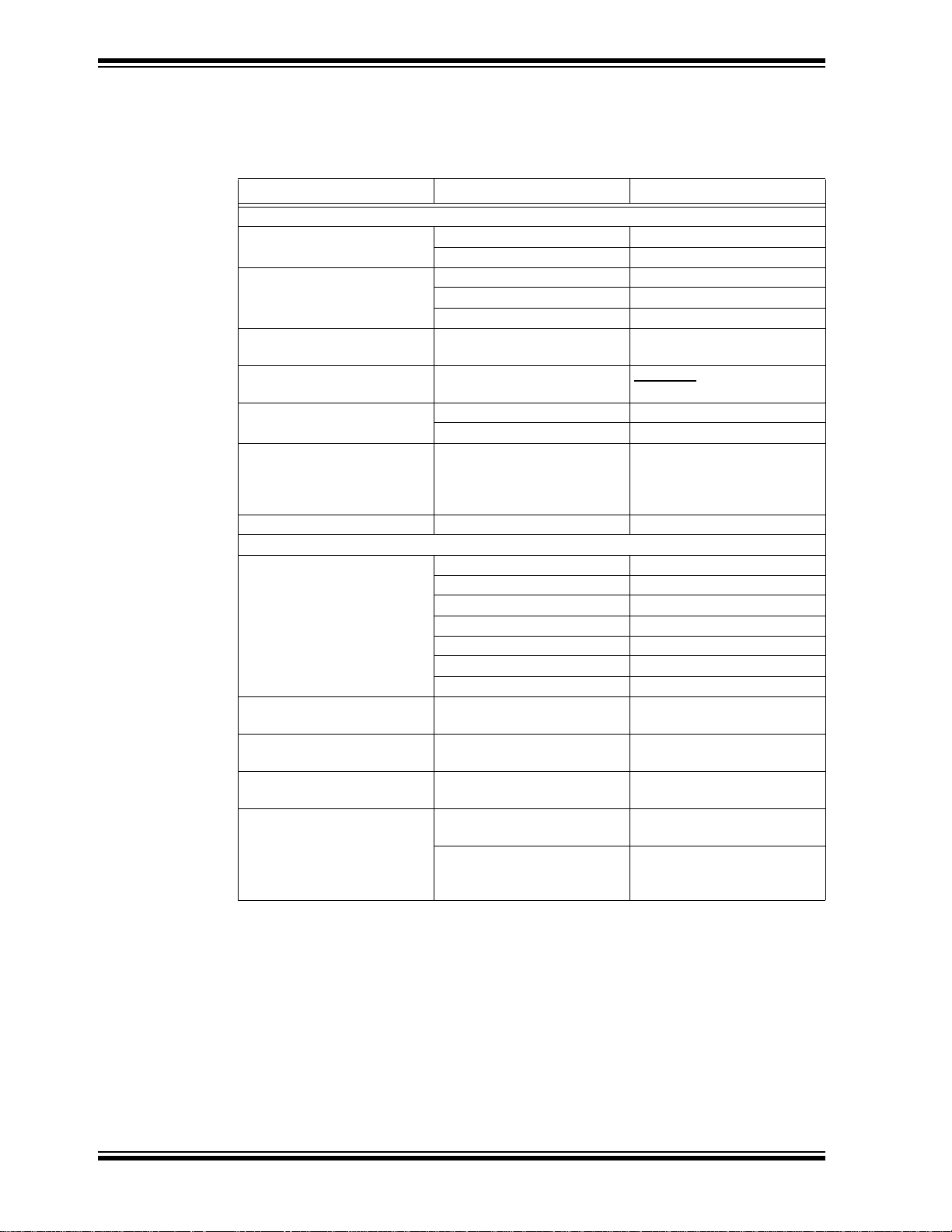
CONVENTIONS USED IN THIS GUIDE
This manual uses the following documentation conventions:
DOCUMENTATION CONVENTIONS
Description Represents Examples
Arial font:
Italic characters Referenced books MPLAB® IDE User’s Guide
Emphasized text ...is the only compiler...
Initial caps A window the Output window
A dialog the Settings dialog
A menu selection select Enable Programmer
Quotes A field name in a window or
dialog
Underlined, italic text with
right angle bracket
Bold characters A dialog button Click OK
N‘Rnnnn A number in verilog format,
Text in angle brackets < > A key on the keyboard Press <Enter>, <F1>
Courier New font:
Plain Courier New Sample source code #define START
Italic Courier New A variable argument file.o, where file can be
Square brackets [ ] Optional arguments mcc18 [options] file
Curly brackets and pipe
character: { | }
Ellipses... Replaces repeated text var_name [,
A menu path File>Save
A tab Click the Power tab
where N is the total number of
digits, R is the radix and n is a
digit.
Filenames autoexec.bat
File paths c:\mcc18\h
Keywords _asm, _endasm, static
Command-line options -Opa+, -Opa-
Bit values 0, 1
Constants 0xFF, ‘A’
Choice of mutually exclusive
arguments; an OR selection
Represents code supplied by
user
“Save project before build”
4‘b0010, 2‘hF1
any valid filename
[options]
errorlevel {0|1}
var_name...]
void main (void)
{ ...
}
DS51781A-page 2 © 2008 Microchip Technology Inc.
Page 7

RECOMMENDED READING
This user's guide describes how to use MCP3422 Evaluation Board. Other useful
documents are listed below. The following Microchip documents are available and
recommended as supplemental reference resources.
PICkit™ Serial Analyzer User’s Guide, DS51647
Consult this document for instructions on how to use the PICkit Serial Analyzer hardware
and software.
MCP3422 Data Sheet, “18-Bit, Multi-Channel ΔΣ Analog-to-Digital Converter with
2
I
C™ Interface and On-Board Reference”, DS22088
This data sheet provides detailed information regarding the MCP3422 product family.
THE MICROCHIP WEB SITE
Microchip provides online support via our web site at www.microchip.com. This web
site is used as a means to make files and information easily available to customers.
Accessible by using your favorite Internet browser , the web site contains the following
information:
• Product Support – Data sheets and errata, application notes and sample
programs, design resources, user’s guides and hardware support documents,
latest software releases and archived software
• General Technical Support – Frequently Asked Questions (FAQs), technical
support requests, online discussion groups, Microchip consultant program
member listing
• Business of Microchip – Product selector and ordering guides, latest Microchip
press releases, listing of seminars and events, listings of Microchip sales offices,
distributors and factory representatives
Preface
CUSTOMER SUPPORT
Users of Microchip products can receive assistance through several channels:
• Distributor or Representative
• Local Sales Office
• Field Application Engineer (FAE)
• Technical Support
Customers should contact their distributor, representative or field application engineer
(FAE) for support. Lo cal sales offices are also available to help customers. A listing of
sales offices and locations is included in the back of this document.
Technical support is available through the web site at: http://support.microchip.com
DOCUMENT REVISION HISTORY
Revision A (November 2008)
• Initial Release of this Document.
© 2008 Microchip Technology Inc. DS51781A-page 3
Page 8

MCP3422 Evaluation Board for PICkit™ Serial User’s Guide
NOTES:
DS51781A-page 4 © 2008 Microchip Technology Inc.
Page 9

MCP3422 EVALUATION BOARD FOR
PICkit™ SERIAL USER’S GUIDE
Chapter 1. Quick Start Instructions
1.1 INTRODUCTION
The following sections provide an overview of the MCP3422 Evaluation Board and
demonstrate how to use it with the PICkit™ Serial Analyzer (P/N: DV164122).
The following topics are covered:
• Description of the MCP3422 Evaluation Board
• How to use the MCP3422 Evaluation Board with the PICkit Serial Analyzer
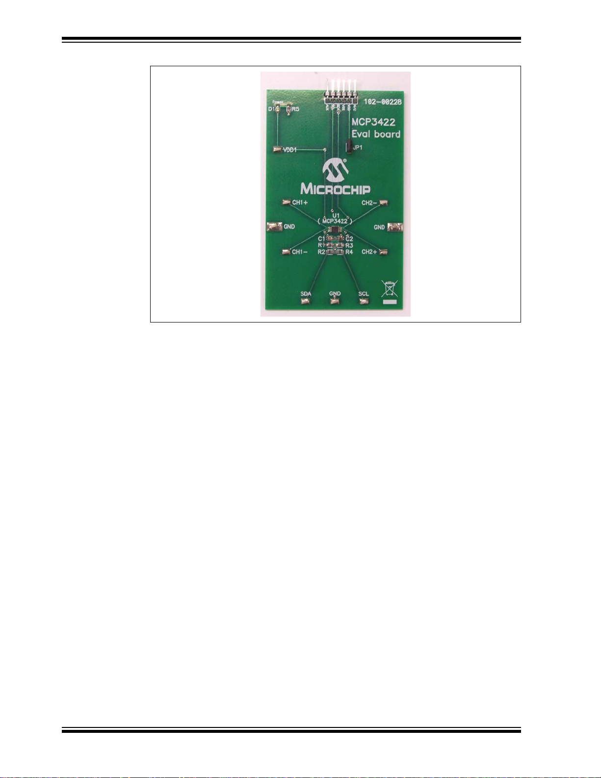
1.2 DESCRIPTION OF THE MCP3422 EVALUATION BOARD
The MCP3422 Evaluation Board (P/N MCP3422EV) contains a MCP3422 18-Bit
Delta-Sigma Analog-to-Digital Converter (ADC). The MCP3422 is a 2-channel ADC
device with various options. The MCP3422 Evaluation Board has analog inpu t
connection pads and V
test the conversion results using the PICkit Serial Analyzer and its PC graphic user
interface (GUI). The MCP3422 Evaluation Board has the following interface:
• PICkit Serial Analyzer for writing configuration register bits and reading the
conversion data.
, SDA, and SCL test pads. The user can connect inputs an d
DD
Note: The MCP3422 Evaluation Board can be used without the PICkit Serial
Analyzer as long as the V
MCP3422 Evaluation Board does not include MCU.
The user can monitor the I
SDA and SCL test pads. Refer to Appendix A. “Schematic and Layouts”.
2C
communications by connecting an oscilloscope to the
, SCL, and SDA are provided to the board. The
DD
1.2.1 I2C Address Bits for the MCP3422
The I2C device code and address bits of the MCP3422 device are programmed at
factory:
• Device Code: ‘1101’
• A2, A1, A0 Address Bits: the MCP3422 device in the MCP3422 Evaluation Boar d
uses default setting: (A2, A1, A0) = (0, 0, 0)
• Address Byte = 1101000R/W
© 2008 Microchip Technology Inc. DS51781A-page 5
Page 10
MCP3422 Evaluation Board for PICkit™ Serial User’s Guide
FIGURE 1-1: Front View of the MCP3422 Evaluation Board.
1.3 GETTING STARTED WITH THE PICKIT SERIAL ANALYZER
Figure 1-1 shows the MCP3422 Evaluation Board and Figure 1-2 shows the MCP3422
Evaluation Board and PICkit Serial Analyzer.
The following instructions describe how to use them together:
1. Connect the MCP3422 Evaluation Board’s 6-pin socket to the PICkit Serial
Analyzer, as shown in Figure 1-2.
2. Connect the oscilloscope probes to the SCL and SDA test pins (optional).
3. V
4. Connecting V
5. Connecting the analog inputs: If you need to measure a single-ended input,
• Connecting the inputs: The MCP3422 Evaluation Board has input pads for
Selection: You can use the VDD from the PICkit Serial Analyzer or you can
DD
use your own external V
(a) Connect JP1, if using V
(b) Disconnect JP1 and apply V
: LED D1 turns on when VDD is applied. The PICkit Serial
DD
Analyzer will provide V
. The JP1 connector selects the VDD path.
DD
from PICkit Serial Analyzer.
DD
at VDD1 pin, if you are using an external VDD.
DD
automatically, if it is connected to the PC. Make sure
DD
LED D1 turns on, when you execute the command using the PICkit Serial
Analyzer.
connect the unused pin (example, CHX-) to V
SS
.
analog inputs for each input channel. You can connect all inputs at the same time
and multiplex the input channel using configuration register settings. You can also
leave the unused channel inputs floating.
DS51781A-page 6 © 2008 Microchip Technology Inc.
Page 11

Quick Start Instructions
PICkit Serial Analyzer
MCP3422 Evaluation Board
USB Cable
Connected between the
and Personal Computer
PICkit Serial analyzer
Personal Computer
Sensor Input
Connectors
Sensor Input
Connectors
6. Use the PICkit Serial Analyzer PC GUI to send I2C write and read commands.
CAUTION
Each analog input pin has an ESD diode. Certain input conditions can damage the
device. Please follow the conditions below:
(a) Do not apply an input greater than the input range specified by the MCP3422 Data
Sheet.
(b) Apply the input signal after V
is powered-up.
DD
FIGURE 1-2: MCP3422 Evaluation Board with the PICkit Serial Analyzer.
© 2008 Microchip Technology Inc. DS51781A-page 7
Page 12

MCP3422 Evaluation Board for PICkit™ Serial User’s Guide
1.3.1 PICkit Serial Analyzer PC Software Setup for the MCP3422
Evaluation Board
The following steps describe how to set up and use the PICkit Serial Analyzer PC
Graphic User Interface (GUI).
1. Install the PICkit Serial Analyzer software onto your personal computer (PC).
2. Connect the USB cable between the PICkit Serial Analyzer and the PC.
3. Run the PICkit Serial PC Software. The following graphic user interface (GUI) will
appear.
FIGURE 1-3: PICkit Serial Analyzer Configuration Wizard Welcome Window.
Click the Next button and follow the instructions.
DS51781A-page 8 © 2008 Microchip Technology Inc.
Page 13

Quick Start Instructions
4. Select the Communication Mode type: I2C Master, and click the Next button.
FIGURE 1-4: Step 1 - Communication Mode Selection.
5. Select 100 kHz or 400 kHz. Either one will be fine. Click the Next button.
2
FIGURE 1-5: Step 2 - I
Note: The MCP3422 device supports the I2C bus data rate up to 3.4 MHz, but the
current version of the PICkit Serial Analyzer supports the I
up to 400 kHz only.
© 2008 Microchip Technology Inc. DS51781A-page 9
C Communication Speed Window.
2
C bus data rate
Page 14

MCP3422 Evaluation Board for PICkit™ Serial User’s Guide
6. Select No on the Enable Pull-ups screen and click the Next button.
Note: The MCP3422 Evaluation Board has its own pull-up resistors.
FIGURE 1-6: Step 3 - Device Pullups Window.
7. Select the V
button.
voltage of the MCP3422 Evaluation Board and click the Next
DD
Case 1: When using VDD from the PICkit Serial Analyzer:
If you choose PICkit Serial will power your device and 5 Volt as shown in
Figure 1-7, the MCP3422 Evaluation Board will be powered by the 5V DC from
the PICkit Serial Analyzer through the JP1 jumper. In this case, make sure that
the JP1 jumper on the MCP3422 Evaluation Board is connected.
Case 2: When using your own VDD:
Y ou can also provide your own VDD voltage by applying a VDD voltage at the VD1
test point. In this case, make sure that the JP1 jumper is disconnected.
DS51781A-page 10 © 2008 Microchip Technology Inc.
Page 15

Quick Start Instructions
FIGURE 1-7: Step 4 - Voltage Source Selection Window.
8. Click the OK button. You have made all the PICkit Serial Analyzer configuration
setups. You are now ready to program the MCP3422 Evalua tion Board using the
PICkit Serial Analyzer.
FIGURE 1-8: Configuration Wizard - Finishing Step.
© 2008 Microchip Technology Inc. DS51781A-page 11
Page 16

MCP3422 Evaluation Board for PICkit™ Serial User’s Guide
1.3.2 Creating Script Files
In order to make a communication connection between the PICkit Seria l Analyzer and
the MCP3422 Evaluation Board, a script file is needed. The followin g procedure shows
how to create script files and how to use them.
• In the PICkit Serial Analyzer window, select from the menu Communications>
Script>Script Builder (Figure 1-9).
FIGURE 1-9: Creating a Script File with Script Builder.
1.3.2.1 CREATING A SCRIPT FILE FOR CONFIGURATION BYTE WRITING
1. Click on WriteBlockAddrA8 in “Example I
This will result in filling in the spaces under the “Script Detail” column. You can
now modify the “Script Detail” column parameters by right-clicking the mouse.
How to modify the parameters box in Script Details:
1. Under the “Script Detail” box, select the item in the parameter box.
2. Right-click the mouse button and an option box appears to the right of your
selection, displaying the options available for the selected parameter.
3. Select the desired option and delete or insert the parameter box.
4. Keep the parameters in the order shown in Figure 1-10.
DS51781A-page 12 © 2008 Microchip Technology Inc.
2
C Scripts” column.
Page 17

Quick Start Instructions
1. To change value:
• Click this box and type a
new number.
2. To delete or insert box:
• Choose the box and
right-click the mouse button for
options available
3. Make sure the listed parameters
in “Script Detail” should be in
exact order as shown here.
I2CSTART *
I2CWRTBYT *
02
D0
9C
I2CSTOP *
Script Detail
------> This means there are two bytes to send
------> 1st Write Byte: Address byte with W/R bit = 1101-0000
------> 2nd Write Byte (Configuration Byte): 1001-1100
FIGURE 1-10: Modifying Parameters in Script Builder Window.
© 2008 Microchip Technology Inc. DS51781A-page 13
4. Change the parameter value.
Note: All 6 parameters above must be listed in the same order as shown here.
The parameters above with * are not modifiable.
Page 18

MCP3422 Evaluation Board for PICkit™ Serial User’s Guide
2 Bytes to send
Address Byte
Configuration Byte
(9C)
Note: The “9C” in the configuration byte selects the following options:
- Conversion Mode: Continuous Conversion
- Channel Selection: Channel 1
- Bit Resolution: 18 bits
- Gain Selection: 1x
FIGURE 1-11: Script File Example for the I2C Write Command.
DS51781A-page 14 © 2008 Microchip Technology Inc.
Page 19

Quick Start Instructions
REDUE THIS PLOT
WITY CORRECT
Write Command with Address bits
Configuration Bits
Zoom-in
Zoom-in
1.3.2.2 SAVING THE SCRIPT FILE AND PROGRAMMING THE MCP3422
CONFIGURATION REGISTER
1. Change the 2nd and 3rd data bytes you want in the Script Detail.
2. Type in any script name (i.e., MCP3422_Write) in the space below the Script
Name menu.
3. Click the Save Script button.
4. Click the Execute Script button.
.
Note: At this point, the PICkit Serial transmits the I
MCP3422 device. The saved file name will appear in “Users I2C Scripts”
column, and can be re-used any time by selecting the file name.
5. You can also see the SCL and SDA waveforms using the oscilloscope.
Note: When you click on the “Execute Script” menu, the “Busy” LED on the PICkit
Serial Analyzer will momentarily turn on and then turn off. If the LED
remains ON, a communications problem has occurred. Remove the PICkit
Serial Analyzer from your computer and re-check the parameter values
including the order of parameters under the “Script Detail” column, and try
again until the “Busy” LED turns OFF immediately after sending the I2C
command.
2
C Write Command to the
FIGURE 1-12: I2C Write Command Waveforms for the MCP3422.
© 2008 Microchip Technology Inc. DS51781A-page 15
Page 20

MCP3422 Evaluation Board for PICkit™ Serial User’s Guide
I2CSTART
I2CWRTBYT
01
D1
I2CRDBYTNLB
I2CSTOP
Script Detail
------> This means there is one byte for address
------> Address byte with W/R bit = 1101-0001
------> 5 bytes to read
5
*
*
*
*
Requesting
Address Byte
5 Bytes
1.3.3 Reading the Conversion Data using the PICkit Serial Analyzer
You can read back the conversion data by following the next steps.
1.3.3.1 CREATING A SCRIPT FILE TO READ THE CONVERSION DATA
1. Click on ReadAddrA8 in “Example I2C Scripts” column.
This will result in filling in the spaces under the “Script Detail”column. Now you
can modify the parameter boxes (delete or insert) in the “Script Detail” column
with options. The list of options will appear if you click with the right mouse button
on the parameter box. You can delete the parameter box or add a new one.
2. Make sure the Script Detail parameters are listed in order as follows:
Note: All 7 parameters above must be listed in order. The parameters above with
* are not modifiable.
FIGURE 1-13: Script File Sample to Read Conversion Data.
DS51781A-page 16 © 2008 Microchip Technology Inc.
Page 21

Quick Start Instructions
3. Type in any scr ipt name (i.e., MCP3422_Read) in the space below the Script
Name menu.
4. Click the Save Script button.
5. Click the Execute Script button.
.
Note: At this point, the PICkit Serial transmits the I
MCP3422 device. The saved file name will appear in the “Users I2C
Scripts” column, and can be re-used any time by selecting the file name.
6. You can also see the SCL and SDA waveforms using the oscilloscope.
Note: When you click on the Execute Script menu, the “Busy” LED on the PICkit
Serial Analyzer will momentarily turn on and then turn off. If the LED
remains ON, a communications problem has occurred. Remove the PICkit
Serial Analyzer from your computer and re-check the parameter values,
including the order of parameters under the “Script Detail” column, and try
again until the “Busy” LED turns OFF immediately after sending the I2C
command.
2
C Read Command to the
© 2008 Microchip Technology Inc. DS51781A-page 17
Page 22

MCP3422 Evaluation Board for PICkit™ Serial User’s Guide
Requesting
5 Bytes
Reading Data
using a Read Command
Address Byte
Results:
Output code: F907 in hex ( = 63751 in decimal)
Output Voltage=
63751
15.625 μVLSB()
PGA
--------------------------------------------
× 0.996 Volts with PGA 1==
Note that if the differential input voltage is negative (CH- > CH+), the MSB of the first byte will be "1 ". In this case, the
voltage is calculated after converting the output code to 2's complement and then multiply the LSB.
See Section 4.9 of the MCP3422 Data Sheet (DS22088) for more information.
5th Byte: Repeated Byte for Configuration byte
4th byte: Configuration Byte (note that RDYbit is “0”)
3rd byte: Data Byte
2nd byte: Data Byte
1st byte: Data Byte
FIGURE 1-14: Reading Conversion Results. Note that the Input = 0.996V is applied at Ch.1. The
reading indicates the measured value is 0.996 Volts.
DS51781A-page 18 © 2008 Microchip Technology Inc.
Page 23

Quick Start Instructions
Zoom-in
Data Bytes = 00F907 (hex)
Zoom-in
Configuration Byte (4th) and Repeated Configuration Byte (5th)
(a) Read command and outputs. The 3 data bytes are zoomed in for better clarity.
(b) Read command and outputs. The last two data bytes are zoomed in for better clarity.
4th Byte
5th Byte
FIGURE 1-15: Read Command and Data on I2C bus. Note the RDY bit in 4th byte is “0”. This means
the conversion data just read is the latest conversion data. The RDY
(repeated byte). This means the device is now in the process of new conversion and the new result is not
ready yet.
© 2008 Microchip Technology Inc. DS51781A-page 19
bit becomes “1” in the 5th byte
Page 24

MCP3422 Evaluation Board for PICkit™ Serial User’s Guide
1.3.4 Experiment with inputs at CH2
Repeat instructions from Section 1.3.2 “Creating Script Files” to
Section 1.3.3 “Reading the Conversion Dat a using the PICkit Serial Analyzer” for
the Channel 2 input.
Note: To write the configuration register for channel 2 input, you can just use the
“MCP3422_Write” file and modify the configuration byte data only.
To read the conversion data, use the same script file for all channels.
DS51781A-page 20 © 2008 Microchip Technology Inc.
Page 25

Appendix A. Schematic and Layouts
A.1 INTRODUCTION
This appendix contains the following schematics and layouts for the MCP3422
Evaluation Board:
• Board – Schematic
• Board – Top Layer
• Board – Top Metal Layer
• Board – Bottom Layer
MCP3422 EVALUATION BOARD FOR
PICkit™ SERIAL USER’S GUIDE
© 2008 Microchip Technology Inc. DS51781A-page 21
Page 26

MCP3422 Evaluation Board for PICkit™ Serial User’s Guide
A.2 BOARD SCHEMATIC
DS51781A-page 22 © 2008 Microchip Technology Inc.
Page 27

A.3 BOARD – TOP LAYER
Schematic and Layouts
© 2008 Microchip Technology Inc. DS51781A-page 23
Page 28

MCP3422 Evaluation Board for PICkit™ Serial User’s Guide
A.4 BOARD – TOP METAL LAYER
DS51781A-page 24 © 2008 Microchip Technology Inc.
Page 29

A.5 BOARD – BOTTOM LAYER
Schematic and Layouts
© 2008 Microchip Technology Inc. DS51781A-page 25
Page 30

MCP3422 Evaluation Board for PICkit™ Serial User’s Guide
NOTES:
DS51781A-page 26 © 2008 Microchip Technology Inc.
Page 31

MCP3422 EVALUATION BOARD FOR
PICkit™ SERIAL USER’S GUIDE
Appendix B. Bill Of Materials (BOM)
TABLE B-1: BILL OF MATERIALS
Qty Reference Description Manufacturer Part Number
1 C1 CAP .1UF 25V CERAMIC X7R
0805
1 C2 CAP CERAMIC 10UF 6.3V X5R
0805
1 D1 LED RED ORANGE CLEAR 0805
SMD
1 J1 CONN HEADER 6POS .100 R/A
TIN
1 JP1 CONN HEADER 2POS .100 VERT
TIN
1 JP1 Shunt .100" Shorting Block with Handle JAMECO VALUEPRO 2012JH-R
1 PCB RoHS Compliant Bare PCB,
MCP3422 Eval Board for PICKit
Serial
2 R1, R3 RES 4.99K OHM 1/8W 1% 0805
SMD
2 R2, R4 DO NOT POPULATE — —
1 R5 RES 470 OHM 1/8W 5% 0805 SMD Panasonic - ECG ERJ-6GEYJ471V
1 U1 2 Channel 18 Bit Data Sigma ADC Microchip Technology Inc MCP3422-E/MS
10 VDD1, CH1+,
CH1-, CH2+,
CH2-, SDA,
SCL, GND
TEST POINT PC COMPACT SMT Keystone Electronics® 5016
Note: The components listed in this Bill of Materials are representative of the PCB assembly. The
released BOM used in manufacturing uses all RoHS-compliant components.
Panasonic® - ECG ECJ-2VB1E104K
Panasonic - ECG ECJ-2FB0J106K
LITE-ON INC LTST-C170EKT
Molex®/Waldom® Electronics
Corp
Molex/Waldom Electronics
Corp
— 104-00228
Microchip Technology Inc. ERJ-6ENF4991V
22-05-2061
22-03-2021
© 2008 Microchip Technology Inc. DS51781A-page 27
Page 32

WORLDWIDE SALES AND SERVICE
AMERICAS
Corporate Office
2355 West Chandler Blvd.
Chandler, AZ 85224-6199
Tel: 480-792-7200
Fax: 480-792-7277
Technical Support:
http://support.microchip.com
Web Address:
www.microchip.com
Atlanta
Duluth, GA
Tel: 678-957-9614
Fax: 678-957-1455
Boston
Westborough, MA
Tel: 774-760-0087
Fax: 774-760-0088
Chicago
Itasca, IL
Tel: 630-285-0071
Fax: 630-285-0075
Dallas
Addison, TX
Tel: 972-818-7423
Fax: 972-818-2924
Detroit
Farmington Hills, MI
Tel: 248-538-2250
Fax: 248-538-2260
Kokomo
Kokomo, IN
Tel: 765-864-8360
Fax: 765-864-8387
Los Angeles
Mission Viejo, CA
Tel: 949-462-9523
Fax: 949-462-9608
Santa Clara
Santa Clara, CA
Tel: 408-961-6444
Fax: 408-961-6445
Toronto
Mississauga, Ontario,
Canada
Tel: 905-673-0699
Fax: 905-673-6509
ASIA/PACIFIC
Asia Pacific Office
Suites 3707-14, 37th Floor
Tower 6, The Gateway
Harbour City, Kowloon
Hong Kong
Tel: 852-2401-1200
Fax: 852-2401-3431
Australia - Sydney
Tel: 61-2-9868-6733
Fax: 61-2-9868-6755
China - Beijing
Tel: 86-10-8528-2100
Fax: 86-10-8528-2104
China - Chengdu
Tel: 86-28-8665-5511
Fax: 86-28-8665-7889
China - Hong Kong SAR
Tel: 852-2401-1200
Fax: 852-2401-3431
China - Nanjing
Tel: 86-25-8473-2460
Fax: 86-25-8473-2470
China - Qingdao
Tel: 86-532-8502-7355
Fax: 86-532-8502-7205
China - Shanghai
Tel: 86-21-5407-5533
Fax: 86-21-5407-5066
China - Shenyang
Tel: 86-24-2334-2829
Fax: 86-24-2334-2393
China - Shenzhen
Tel: 86-755-8203-2660
Fax: 86-755-8203-1760
China - Wuhan
Tel: 86-27-5980-5300
Fax: 86-27-5980-5118
China - Xiamen
Tel: 86-592-2388138
Fax: 86-592-2388130
China - Xian
Tel: 86-29-8833-7252
Fax: 86-29-8833-7256
China - Zhuhai
Tel: 86-756-3210040
Fax: 86-756-3210049
ASIA/PACIFIC
India - Bangalore
Tel: 91-80-4182-8400
Fax: 91-80-4182-8422
India - New Delhi
Tel: 91-11-4160-8631
Fax: 91-11-4160-8632
India - Pune
Tel: 91-20-2566-1512
Fax: 91-20-2566-1513
Japan - Yokohama
Tel: 81-45-471- 6166
Fax: 81-45-471-6122
Korea - Daegu
Tel: 82-53-744-4301
Fax: 82-53-744-4302
Korea - Seoul
Tel: 82-2-554-7200
Fax: 82-2-558-5932 or
82-2-558-5934
Malaysia - Kuala Lumpur
Tel: 60-3-6201-9857
Fax: 60-3-6201-9859
Malaysia - Penang
Tel: 60-4-227-8870
Fax: 60-4-227-4068
Philippines - Manila
Tel: 63-2-634-9065
Fax: 63-2-634-9069
Singapore
Tel: 65-6334-8870
Fax: 65-6334-8850
Taiwan - Hsin Chu
Tel: 886-3-572-9526
Fax: 886-3-572-6459
Taiwan - Kaohsiung
Tel: 886-7-536-4818
Fax: 886-7-536-4803
Taiwan - Taipei
Tel: 886-2-2500-6610
Fax: 886-2-2508-0102
Thailand - Bangkok
Tel: 66-2-694-1351
Fax: 66-2-694-1350
EUROPE
Austria - Wels
Tel: 43-7242-2244-39
Fax: 43-7242-2244-393
Denmark - Copenhagen
Tel: 45-4450-2828
Fax: 45-4485-2829
France - Paris
Tel: 33-1-69-53-63-20
Fax: 33-1-69-30-90-79
Germany - Munich
Tel: 49-89-627-144-0
Fax: 49-89-627-144-44
Italy - Milan
Tel: 39-0331-742611
Fax: 39-0331-466781
Netherlands - Drunen
Tel: 31-416-690399
Fax: 31-416-690340
Spain - Madrid
Tel: 34-91-708-08-90
Fax: 34-91-708-08-91
UK - Wokingham
Tel: 44-118-921-5869
Fax: 44-118-921-5820
01/02/08
DS51781A-page 28 © 2008 Microchip Technology Inc.
 Loading...