

Page 1

MCP2210
Evaluation Kit
User’s Guide
© 2012 Microchip Technology Inc. DS52057A
Page 2

Note the following details of the code protection feature on Microchip devices:
• Microchip products meet the specification contained in their particular Microchip Data Sheet.
• Microchip believes that its family of products is one of the most secure families of its kind on the market today, when used in the
intended manner and under normal conditions.
• There are dishonest and possibly illegal methods used to breach the code protection feature. All of these methods, to our
knowledge, require using the Microchip products in a manner outside the operating specifications contained in Microchip’s Data
Sheets. Most likely, the person doing so is engaged in theft of intellectual property.
• Microchip is willing to work with the customer who is concerned about the integrity of their code.
• Neither Microchip nor any other semiconductor manufacturer can guarantee the security of their code. Code protection does not
mean that we are guaranteeing the product as “unbreakable.”
Code protection is constantly evolving. We at Microchip are committed to continuously improving the code protection features of our
products. Attempts to break Microchip’s code protection feature may be a violation of the Digital Millennium Copyright Act. If such acts
allow unauthorized access to your software or other copyrighted work, you may have a right to sue for relief under that Act.
Information contained in this publication regarding device
applications and t he lik e is provided only for your convenience
and may be su perseded by upda t es . It is y our responsibility to
ensure that your application meets with your specifications.
MICROCHIP MAKES NO REPRESENTATIONS OR
WARRANTIES OF ANY KIND WHETHER EXPRESS OR
IMPLIED, WRITTEN OR ORAL, STATUTORY OR
OTHERWISE, RELATED TO THE INFORMATION,
INCLUDING BUT NOT LIMITED TO ITS CONDITION,
QUALITY, PERFORMANCE, MERCHANTABILITY OR
FITNESS FOR PURPOSE. Microchip disclaims all liability
arising from this information and its use. Use of Microchip
devices in life supp ort and/or safety ap plications is entir ely at
the buyer’s risk, and the buyer agrees to defend, indemnify and
hold harmless M icrochip from any and all dama ges, claims,
suits, or expenses re sulting from such use. No licens es are
conveyed, implicitly or otherwise, under any Microchip
intellectual property rights.
Trademarks
The Microchip name and logo, the Microchip logo, dsPIC,
K
EELOQ, KEELOQ logo, MPLAB, PIC, PICmicro, PICSTART,
32
PIC
logo, rfPIC and UNI/O are registered trademarks of
Microchip Technology Incorporated in the U.S.A. and other
countries.
FilterLab, Hampshire, HI-TECH C, Linear Active Thermistor,
MXDEV, MXLAB, SEEVAL and The Embedded Control
Solutions Company are registered trademarks of Microchip
Technology Incorporated in the U.S.A.
Analog-for-the-Digital Age, Application Maestro, chipKIT,
chipKIT logo, CodeGuard, dsPICDEM, dsPICDEM.net,
dsPICworks, dsSPEAK, ECAN, ECONOMONITOR,
FanSense, HI-TIDE, In-Circuit Serial Programming, ICSP,
Mindi, MiWi, MPASM, MPLAB Certified logo, MPLIB,
MPLINK, mTouch, Omniscient Code Generation, PICC,
PICC-18, PICDEM, PICDEM.net, PICkit, PICtail, REAL ICE,
rfLAB, Select Mode, Total Endurance, TSHARC,
UniWinDriver, WiperLock and ZENA are trademarks of
Microchip Technology Incorporated in the U.S.A. and other
countries.
SQTP is a service mark of Microchip Technology Incorporated
in the U.S.A.
All other trademarks mentioned herein are property of their
respective companies.
© 2012, Microchip Technology Incorporated, Printed in the
U.S.A., All Rights Reserved.
Printed on recycled paper.
ISBN: 978-1-62076-118-2
QUALITY MANAGEMENT SYSTEM
CERTIFIED BY DNV
== ISO/TS 16949 ==
Microchip received ISO/TS-16949:2009 certification for its worldwide
headquarters, design and wafer fabrication facilities in Chandler and
Tempe, Arizona; Gresham, Oregon and design centers in California
and India. The Company’s quality system processes and procedures
are for its PIC
devices, Serial EEPROMs, microperipherals, nonvolatile memory and
analog products. In addition, Microchip’s quality system for the design
and manufacture of development systems is ISO 9001:2000 certified.
®
MCUs and dsPIC® DSCs, KEELOQ
®
code hopping
DS52057A-page 2 © 2012 Microchip Technology Inc.
Page 3

MCP2210 EVALUATIO N KI T
USER’S GUIDE
Table of Contents
Preface ...........................................................................................................................5
Introduction............................................................................................................5
Document Layout .................................................................................................. 5
Conventions Used in this Guide............................................................................ 6
Recommended Reading.............................................................. .. ........................7
The Microchip Web Site........................................................................................ 7
Customer Support....................... ....................................................... ...................7
Document Revision History................................................................................... 7
Chapter 1. Product Overview
1.1 Introduction .....................................................................................................9
1.2 MCP2210 Evaluation Kit General Description ................ .. ........................ .. ....9
1.3 What The MCP2210 Evaluation Kit Includes ................................................. 9
Chapter 2. Installation and Operation
2.1 Introduction ...................................................................................................11
2.2 Kit Setup ....................................................................................................... 11
2.3 Board Oper a tio n .. .. ............................. .......................................................... 12
2.4 MCP2210 Typical Usage Scenarios ...................... .. .....................................17
Appendix A. Schematic and Layouts
A.1 Introduction ..................................................................................................19
A.2 MCP2210 Breakout Board Schematic and Layouts .....................................20
A.3 MCP2210 SPI Slave Motherboard Schematic and Layouts ........................27
Appendix B. Bill of Materials
Worldwide Sales and Service ....................................................................................36
© 2012 Microchip Technology Inc. DS52057A-page 3
Page 4

MCP2210 Evaluation Kit User’s Guide
NOTES:
DS52057A-page 4 © 2012 Microchip Technology Inc.
Page 5

MCP2210 EVALUATIO N KI T
USER’S GUIDE
Preface
NOTICE TO CUSTOMERS
All documentation becomes dated, and this manual is no exception. Microchip tools and
documentation are constantly evolving to meet customer needs, so some actual dialogs
and/or tool descriptions may differ from those in this document. Please refer to our web site
(www.microchip.com) to obtain the latest documentation available.
Documents are identified with a “DS” number. This number is located on the bottom of each
page, in front of the p age number. The numbering convention for the DS number is
“DSXXXXXA”, where “XXXXX” is the document number and “A” is the revision level of the
document.
For the most up-to-date information on development tools, see the MPLAB
Select the Help menu, and then Topics to open a list of available online help files.
®
IDE online help.
INTRODUCTION
This chapter contains general information that will be useful to know before using the
MCP2210 Evaluation Kit. Items discussed in this chapter include:
• Document Layout
• Conventions Used in this Guide
• Recommended Reading
• The Microchip Web Site
• Customer Support
• Document Revision History
DOCUMENT LAYOUT
This document describes how to use the MCP2210 Evaluation Kit as a development
tool. The manual layout is as follows:
• Chapter 1. “Product Overview” – Important information about the MCP2210
Evaluation Kit
• Chapter 2. “Installation and Operation” – Covers the initial set-up of this board
and Graphical User Interface (GUI)
• Appendix A. “Schematic and Layouts” – Shows the schematic and board
layouts for the MCP2210 Evaluation Kit User’s Guide
• Appendix B. “Bill of Materials” – Lists the parts used to populate the MCP2210
Evaluation Kit
© 2012 Microchip Technology Inc. DS52057A-page 5
Page 6
MCP2210 Evaluation Kit User’s Guide
CONVENTIONS USED IN THIS GUIDE
This manual uses the following docum entat io n conven tion s:
DOCUMENTATION CONVENTIONS
Description Represents Examples
Arial font:
Italic chara c ters Referenced books MPLAB
Emphasized text ...is the only compiler...
Initial caps A window the Output window
A dialog the Settings dialog
A menu selection select Enable Programmer
Quotes A field name in a window or
dialog
Underlined, italic text with
right angle bracket
Bold characters A dialog button Click OK
N‘Rnnnn A number in verilog format,
Text in angle brac kets < > A key on the keyboard Press <Enter>, <F1>
Courier New font:
Plain Courier New Sample source code #define START
Italic Courier New A variable argument file.o, where file can be
Square brackets [ ] Optional arguments mcc18 [options] file
Curly brackets and pipe
character: { | }
Ellipses... Replaces r epeated text var_name [,
A menu path File>Save
A tab Click the Power tab
where N is the tota l number of
digits, R is th e radi x and n is a
digit.
Filenames autoexec.bat
File paths c:\mcc18\h
Keywords _asm, _endasm, static
Command-line options -Opa+, -Opa-
Bit values 0, 1
Constants 0xFF, ‘A’
Choice of mut ually exclus ive
arguments; an OR selection
Represents code supplied by
user
®
IDE User’s Guide
“Save project before build”
4‘b0010, 2‘hF1
any valid filename
[options]
errorlevel {0|1}
var_name...]
void main (void)
{ ...
}
DS52057A-page 6 © 2012 Microchip Technology Inc.
Page 7

RECOMMENDED READING
This user's guide describes how to use MCP2210 Evaluation Kit. Other useful
documents are listed below. The following Microchip documents are available and
recommended as supplemental r eference resources.
• MCP2210 Data Sheet - “USB-to-SPI Protocol Converter with GPIO (Master
Mode)” (DS22288)
THE MICROCHIP WEB SITE
Microchip provides online support via our web site at www.microchip.com. This web
site is used as a means to make files and information easily available to customers.
Accessible by using your favorite Internet browser, the web site contains the following
information:
• Product Support – Data sheets and errata, application notes and sample
programs, design resources, user’s guides and hardware support documents,
latest software releases and archived software
• General Technical Support – Frequently Asked Questions (FAQs), technical
support requests, online discussion groups, Microchip consultant program
member listing
• Business of Microchip – Product selector and ordering guides, latest Microchip
press releases, listing of seminars and events, listings of Microchip sales offices,
distributors and factory representatives
Preface
CUSTOMER SUPPORT
Users of Microchip products can receive assistance through several channels:
• Distributor or Representative
• Local Sales Office
• Field Application Engineer (FAE)
• Technical Support
Customers should contact their distributor, representative or field application engineer
(FAE) for support. Local sales offices are also available to help customers. A listing of
sales offices and locations is included in the back of this document.
T echnical support is available through the web site at: .http://www.microchip.com/support.
DOCUMENT REVISION HISTORY
Revision A (March 2012)
• Initial Release of this Document.
© 2012 Microchip Technology Inc. DS52057 A-page 7
Page 8

MCP2210 Evaluation Kit User’s Guide
NOTES:
DS52057A-page 8 © 2012 Microchip Technology Inc.
Page 9

MCP2210 EVALUATIO N KI T
Chapter 1. Product Overview
1.1 INTRODUCTION
This chapter provides an overview of the MCP2210 Evaluation Kit and covers the
following topics:
• MCP2210 Evaluation Kit General Description
• What The MCP2210 Evaluation Kit Includes
1.2 MCP2210 EVALUATION KIT GENERAL DESCRIPTION
The MCP2210 Evaluation Kit (ADM00421) is a development and evaluation platform
for the MCP2210 device. The kit is comprised of two connected boards:
• MCP2210 Breakout Board (ADM00419)
• MCP2210 SPI Slave Motherboard (ADM00420)
The MCP2210 SPI Slave Motherboard is designed to work together with the MCP2210
Breakout Board (ADM00419). The motherboard provides the test-points required for
measurements. It also contains the following SPI slave devices:
• MCP23S08 – 8-bit I/O expander
• MCP3204 – 4 channel, 12-bit ADC
• 25LC02 – 2 kbit EEPROM
• TC77 – Temperature sensor
All devices are SPI slaves, controlled by the MCP2210.
Windows®-based PC software is used to evaluate/demonstrate the MCP2210 as a
USB-to-SPI (Master) device. It allows I/O control and custom device configuration. The
software is downloadable from the board web page on www.microchip.com.
A DLL package is also available for development of custom PC applications using the
MCP2210. The DLL package is downloadable from the board’s web page.
USER’S GUIDE
1.3 WHAT THE MCP2210 EVALUATION KIT INCLUDES
The MCP2210 Evaluation Kit includes (ADM00421):
• MCP2210 Breakout Board (ADM00419)
• MCP2210 SPI Slave Motherboard (ADM00420)
•Mini-USB cable
• Important Information Sheet
© 2012 Microchip Technology Inc. DS52057A-page 9
Page 10

MCP2210 Evaluation Kit User’s Guide
NOTES:
DS52057A-page 10 © 2012 Microchip Technology Inc.
Page 11

Chapter 2. Installation and Operation
2.1 INTRODUCTION
The MCP2210 Evaluation Kit is designed to demonstrate the device as a USB-to-SPI
(Master) bridge solution.
The Evaluation Kit is comprised of two boards that have the following features:
• MCP2210 Breakout Board:
- Small plug-in board with DIP form factor (0.6 inches overall row spacing
between pins)
- Mini-USB co nnector
- Access to the SPI bus and all GP signals
- PICkit™ Serial Analyzer compatible header
- 3.3 or 5V jumper selectable V
up to 500 mA to the rest of the system
• MCP2210 SPI Slave Motherboard:
- Socket for plugging in the MCP2210 Breakout Board
- Test-points for the SPI bus and GP signals
- PICkit™ Serial Analyzer header (it can be used to access only one of the SPI
slave chips present on this board – MCP23S08)
- 8-bit I/O expander (MCP23S08) with eight LEDs
- Four channel, 12-bit ADC (MCP3204) – a potentiometer is used to vary the
voltage on the Channel 1 ADC input
- 2 kbit EEPROM – 25LC02
- Temperature sensor – TC77
MCP2210 EVALUATIO N KI T
USER’S GUIDE
; the Breakout Board can be used to supply
DD
2.2 KIT SETUP
Follow these steps to set up the MCP2210 Evaluation Kit:
1. Download the support material (PC applications and DLL libraries) that can be
found on the board’s page (www.microchip.com/mcp2210evaluationkit).
2. Plug the MCP2210 Breakout Board into the MCP2210 SPI Slave Motherboard.
3. Connect the MCP2210 Breakout Board to a PC via a USB port.
4. The system will automatically install the driver for this board. When the
installation is complete, the board is ready for operation.
5. Install the downloaded PC software.
6. Start the demo application and exercise the SPI slave chip’s features.
© 2012 Microchip Technology Inc. DS52057A-page 11
Page 12

MCP2210 Evaluation Kit User’s Guide
2.3 BOARD OPERATION
The MCP2210 device is detected by a Windows®-based PC host as a Human Interface
Device (HID). The accompanying software can be used to exercise the Evaluation Kit’s
features. It also provides a reference point for users that want to create custom
applications based on the MCP2210.
2.3.1 MCP2210 Breakout Board Operation
The MCP2210 Breakout Board can be used with either the provided motherboard, or
as a stand-alone USB-to-SPI (Master) bridge module. The breakout board provides all
the required signals in order to assist the user in building customized boards using the
MCP2210.
The breakout board has the following features:
• SPI bus signals (MOSI, MISO, SCK)
• 9 GP signals configurable for:
- GPIO functionality (digital input or output pins)
- Chip Select functionality (working with the SPI bus signals)
- Dedicated function pins
• Jumper selectable power supply: 3.3 or 5V (up to 500 mA). The board has a
default connection trace between V
mounting unnecessary when powering the board with 3.3V. For 5V operation, a
3-pin header must be mounted on the board.
• PICkit™ Serial Analyzer header using GP4 as the Chip Select signal
and 3.3V rail, making the voltage header
DD
Note: This function is available only on SPI operations, it does not work on I
UART signals.
• Dip form-factor (0.6 inches overall row spacing between pins)
By using the provided software and libraries, the user can create personalized PC
applications using the breakout board as a USB-to-SPI (Master) bridge adapter.
2
C or
2.3.2 MCP2210 Breakout Board Operation
The MCP2210 Utility software was created for custom device setting requirements. A
few of the settings that this utility can alter include VID, PID, power requirements, and
string descriptors. A download link for this software can be found on the board web
page. For instructions on the use of this software, refer to the software’s supporting
documentation included with in the appl ic at ion install package.
2.3.3 SPI Terminal Utility
The SPI Terminal Utility is a tool that allows low-level data exchange at the SPI bus
level. This application is useful for low-level communication and troubleshooting
between the MCP2210 and various SPI slave modules.
The utility window has different sections for GP designation, SPI transfer parameters
and user data area.
DS52057A-page 12 © 2012 Microchip Technology Inc.
Page 13

FIGURE 2-1: SPI TERMINAL UTILITY WINDOW
SPI user data
section
HEX/Decimal
user data
mode
Installation and Operation
GP Settings Section
SPI Transfer
Parameters
Section
Status messages
After the application is started, the state of the connection with the MCP2210 is shown
in the Status Messages bar (in the lower left corner of the screen).
The user can establish the GP configuration. The GPs can be used as chip select pins.
Each GP Active and Idle value can be established by selecting the appropriate checkboxes, or by directly supplying the correct value in the GP Direct Settings section. The
same behavior applies to the GP designation (the GP designation can be established
by clicking the appropriate radio-button, or by directly supplying the GP designation
value in the GP settings Direct Values section).
The SPI settings pertaining to the needed SPI transfer can be established in the SPI
Parameters section.
The data to be sent out is filled in the Tx Data field. To send the data to the SPI slave
device, press the SPI Transfer Da ta button on the lower right area of the screen. The
data received from the SPI slave device is displayed in the Rx Data field.
The user data can be supplied in either HEX or Decimal mode. This can be
accomplished by selecting the HEX mode checkbox. The data in the Tx and Rx Data
fields will be displayed in HEX or Decimal.
Transfer Data button
GP Direct
Settings section
© 2012 Microchip Technology Inc. DS52057A-page 13
Page 14

MCP2210 Evaluation Kit User’s Guide
A simple test using the SPI Terminal utility shows how the MCP23S08 (an 8-bit I/O
expander) uses the GP4 pin of the MCP2210 device as a chip select line. This line
should be active low. The GP4 must be set as in the Figure 2-1, with the IDLE option
checked (IDLE value is logic ‘1’) and the ACTIVE option unchecked (ACTIVE value is
logic ‘0’).
The SPI parameters are set as follows:
• Bit rate - 500000 bps
• SPI Mode – 0
• Number of bytes to transfer – 3
• All the SPI related delays are set to 0
The TX Data should contain the following HEX values: 40, 00, 00. Click on the SPI
Transfer Data button to complete the procedure and set the MCP23S08’s port as an
output.
After setting this port, a value can be sent out to the port to light the LEDs on the board.
To make this happen, insert the following three HEX values: 40, 0A, FF . By clicking the
SPI Transfer Data button again, the inserted values are sent out to the MCP23S08
device. This command will light all the LEDs on the board. If any other LED light pattern
is desired, the third value (FF) can be changed to any other 8-bit value.
To verify the value written to the MCP23S08’s port, another set of data must be written
into the TX Data area: 41, 0A and any other 8-bit value (a “Don’t care” value for the third
position is admissible, because the read value from the MCP23S08 is received on the
third byte).
In the RX Data field, the third value should be the identical to the one sent out previously (in the given example, FF).
2.3.4 MCP2210 Evaluation Kit demo application
The provided demo application is designed to work with the MCP2210 SPI Slave
Motherboard using the MCP2210 Breakout Board as a USB-to-SPI bridge.
The application’s source code is provided to facilitate the development of custom PC
applications using the MCP2210 and the accompanying DLL package. This application
was written in Visual Basic.
DS52057A-page 14 © 2012 Microchip Technology Inc.
Page 15

Installation and Operation
FIGURE 2-2: VISUAL BASIC APPLICATION WINDOW
I/O Expander
Section
Temperature
Sensor
Section
ADC Section
I/O Expander Section
Selected EEPROM Addr es s
The PC GUI shows typical sections for each of the SPI slave devices present on the
MCP2210 SPI Slave Motherboard.
2.3.5 MCP23S08 GPIO Expander controls
The GUI provides specific controls in order to assist the user in exploring the I/O
expander features. The control for this chip shows eight color-coded buttons, each
representing an I/O option.
FIGURE 2-3: MCP23S08 GPIO EXPANDER SECTION
I/O buttons
By double-clicking on any of the buttons, the assigned I/O pin will toggle from being a
digital input to digital output and back.
For the I/Os designated as digital inputs, any change on the pins will be shown on the
GUI in yellow (for a logic high value) or in blue (for a logic low value).
For the I/Os designated as digital outputs, a single click on any of the I/O circles will
toggle their output value from logic low (in red) to logic high (in green). When a digital
output is set to logic high, the corresponding LED will be lit.
Color coded
reference table
for I/O option
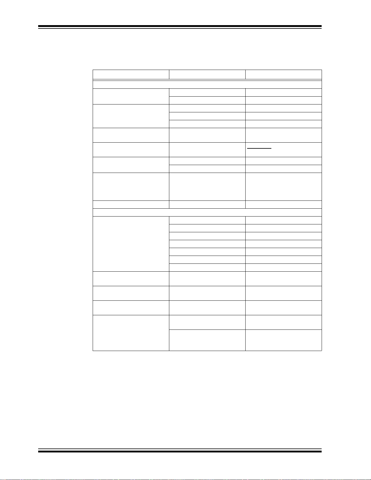
2.3.6 EEPROM 25LC02 Controls
The EEPROM GUI section presents a data-grid control and three buttons (see
Figure 2-4). The data-grid is organized in eight columns and sixty-four rows. The
EEPROM addresses are read from left to right, top to bottom, starting at location 0 (in
© 2012 Microchip Technology Inc. DS52057A-page 15
Page 16
MCP2210 Evaluation Kit User’s Guide
the first line, first column on the left). When, a particular cell in the data grid control is
highlighted, the corresponding EEPROM address is displayed in the bottom left corner
of the application window.
FIGURE 2-4: EEPROM 25LC02 SECTION
Data-grid
controls
Control
buttons
The EEPROM section also shows three buttons :
• Read EEPROM – Press this button to read the entire EEPROM memory. The
content will show in the data-grid control.
• Write EEPROM – The user can modify the data and add other hex-represented
byte values in the cells. When all the modifications are done, press this button to
write the modified data-grid content on the EEPROM.
• Clear Mem – T o verify the EEPROM content, press this button. This action clears
only the data-grid control, not the EEPROM contents. Later, when the Read
EEPROM button is pressed again, the actual EEPROM content will display in the
data-grid control.
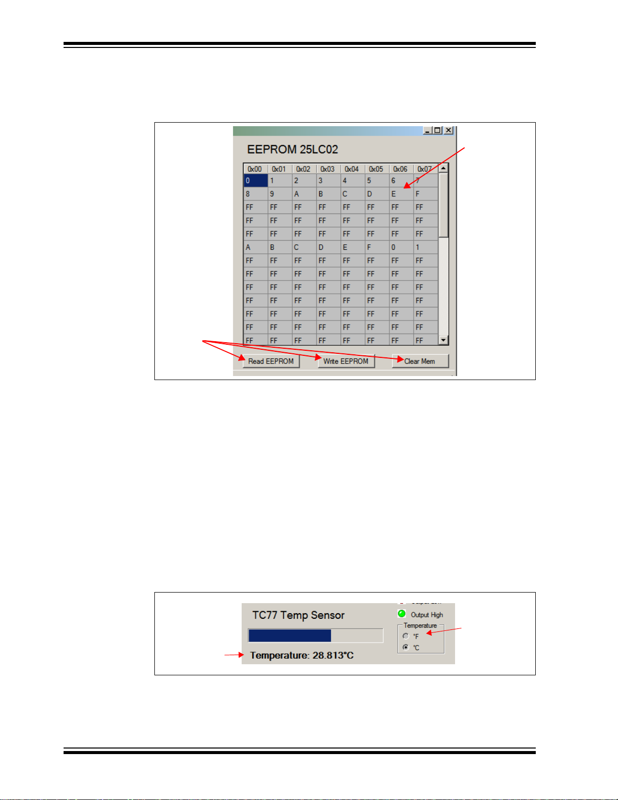
2.3.7 TC77 Temp Sensor Section
The temperature sensor displays the temperature of the sensor device present on the
motherboard in either Fahrenheit or Celsius scales.
FIGURE 2-5: TC77 TEMPERATURE SENSOR SECTION
Temperature
TC77
temperature
unit selection
DS52057A-page 16 © 2012 Microchip Technology Inc.
Page 17

Installation and Operation
2.3.8 MCP3204 ADC Display Section
The MCP3201 12-bit ADC section displays the board’s measured VDD voltage and a
voltage between 0 and V
motherboard potentiometer.
FIGURE 2-6: MCP3204 ADC VALUES DISPLAY
Motherboard
potentiometer
settings display
(between 0 and
and V
DD/2)
Custom voltage
value display
The remaining channels (channels 2 and 3) can also display custom user
measurements of voltages between 0V
DD/2, corresponding to the voltage value set by the
VDD voltage
value display
– 2.5V (maximum).
2.4 MCP2210 TYPICAL USAGE SCENARIOS
The MCP2210 can be used in systems where an SPI bus is available. The MCP2210
device can be either the single master on the bus, or one of the masters sharing the
bus, if a proper master-access arbitration scheme is in place.
In cases where the MCP2210 is the only master on the SPI bus, a typical usage
scenario is shown in Figure 2-7. The SPI bus links the SPI slave chips to the system,
while a few GPs (configured for chip select function) can be used as chip select lines.
If SPI slave interrupt monitoring is required, the GP6 needs to be configured for its
dedicated function, in order to monitor the interrupts coming from the SPI slave chips.
The PC application will handle all the details necessary for data transfer between the
MCP2210 and the SPI slave devices.
© 2012 Microchip Technology Inc. DS52057A-page 17
Page 18

MCP2210 Evaluation Kit User’s Guide
FIGURE 2-7: MCP2210 TYPICAL USAGE DIAGRAM
MCP2210
USB
USB-to-SPI
bridge
External
Interrupt
(GP6)
SPI bus
Chip-Select lines
SPI slave chip #1 SPI slave chip #n
MOSI, MISO, SCK
CS0-CS8
...
Interrupt
When a system requires more than one SPI master sharing the same bus, an
arbitration scheme needs to be developed, to prevent multiple SPI masters trying to
access the bus at the same time. MCP2210 has support for such a mechanism, using
GP7 and GP8 (configured for dedicated pin functionality) for this purpose.
When GP8 is configured for its dedicated functionality, the pin can be used as a bus
release request for MCP2210 coming from another master. GP7 (configured for its dedicated functionality) is used as an SPI bus release acknowledge signal towards the
requesting master. When an external SPI master requests that the MCP2210 release
the bus, the MCP2210 completes the current SPI transfer (or it can be cancelled by the
PC application by sending the proper USB command). Then it releases the bus, and
signals this event on the acknowledge pin (GP7). The second master now has ownership of the bus and can keep it as long as the SPI bus request pin (GP8) is kept
asserted.
In conclusion, when the dedicated functionality of the GP7 and GP8 are used,
MCP2210 can be used in a multiple SPI master system.
Interrupt
DS52057A-page 18 © 2012 Microchip Technology Inc.
Page 19

Installation and Operation
FIGURE 2-8: MCP2210 TYPICAL USAGE DIAGRAM
MCP2210
GP8
GP7
SPI Bus Release Request
SPI Bus Release
Acknowledge
SPI Master #2
USB
USB-toSPI
bridge
External
Interrupt
(GP6)
SPI bus
Chip-Select lines
SPI slave chip #1 SPI slave chip #n
...
Interrupt
Interrupt
MOSI, MISO, SCK
External
Interrupt
© 2012 Microchip Technology Inc. DS52057A-page 19
Page 20

MCP2210 Evaluation Kit User’s Guide
NOTES:
DS52057A-page 20 © 2012 Microchip Technology Inc.
Page 21

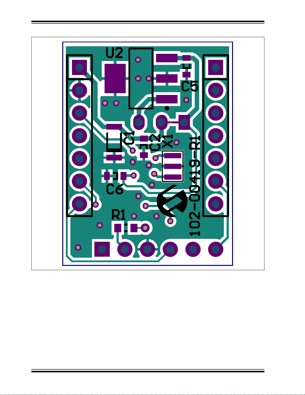
Appendix A. Schematic and Layouts
A.1 INTRODUCTION
This appendix contains the following schematics and layouts for the MCP2210
Evaluation Kit:
• MCP2210 Breakout Board Schematic and Layouts
- Board – Schematic
- Board – Top Silk and Pads
- Board – Top Silk, Pads and Copper
- Board – Top Pads and Copper
- Board – Bottom Silk and Pads
- Board – Bottom Silk, Pads and Copper
- Board – Bottom Pads and Copper
• MCP2210 SPI Slave Motherboard Schematic and Layouts
- Board – Schematic
- Board – Top Silk
- Board – Top Silk and Copper
- Board – Top Copper
- Board – Bottom Silk
- Board – Bottom Silk and Copper
MCP2210 EVALUATIO N KI T
USER’S GUIDE
© 2012 Microchip Technology Inc. DS52057A-page 19
Page 22

MCP2210 Evaluation Kit User’s Guide
S
T
OS
PGP
US
S
BU
OU
T
G
D
A.2 MCP2210 BREAKOUT BOARD SCHEMATIC AND LAYOUTS
A.2.1 Board – Schematic
J5
D-2D+
USB_D-
5%390
R1
3
USB_D+
0603
TP1
ID
4
Via_1.2x 0.7
VDD
GND
5
X1
12MHz
USB-B-Mini SMD
GND D
GND D
GND D
GND D
U1
0603
C2
0.1uF
31
2
GP8
GP7
GP6
GP5
MI SO
0603
1uF
C6
VUSB
USB_D-
USB_D+
18
19
20
D+
VSS
V
VDD1OSC12OSC23RST4GP05GP16GP27GP38MOSI9GP4
VDR
OSC2
OSC1
GND D
13
17
D-
RST
16
VUSB
V
PPP
GP0
GP1
GP614GP715GP8
GP2
MI SO
P
GP3
12
GP5
G
M
MOSI
11
10
SCK
SCK
P
GP4
MCP2210
VBUS
V
1
5V
VDD
VDD
GP8
GP2
GP7
GP3
GP6
GP4
GP5
MOSI
76543
MI SO
SCK
76543
1 x 7 VERT
Right Side Header
HDR M
GND D
HDR M 1x7 VERT
Left Side Header
VDD
SCK
GP4
MOSI
MISO
J3
123456
Serial Analyzer Header
HDR M 1x6 VERT
PICkit™
2
1
J2
VDD
GND D
NT1
VUSB
U2
MCP1825S-3.3V
5V
3.3V
3
1
5V
VOUT
V
VIN
123
GND
N
C4
C3
J4
C5
2
0.1uF
4.7uF
1 x 3 VERT
HDR M
Default connection
0603
0.1uF
0603
0603
between 1 - 2. User to
cut the trace if 5V VDD
GND D
GND D GND D GND D
is needed.
22uF
1206
C1
GND D
GP0
GP1
2
1
J1
DS52057A-page 20 © 2012 Microchip Technology Inc.
Page 23

A.2.2 Board – Top Silk and Pads
Schematic and Layouts
© 2012 Microchip Technology Inc. DS52057A-page 21
Page 24
MCP2210 Evaluation Kit User’s Guide
A.2.3 Board – Top Silk, Pads and Copper
DS52057A-page 22 © 2012 Microchip Technology Inc.
Page 25

A.2.4 Board – Top Pads and Copper
Schematic and Layouts
© 2012 Microchip Technology Inc. DS52057A-page 23
Page 26

MCP2210 Evaluation Kit User’s Guide
A.2.5 Board – Bottom Silk and Pads
DS52057A-page 24 © 2012 Microchip Technology Inc.
Page 27

A.2.6 Board – Bottom Silk, Pads and Copper
Schematic and Layouts
© 2012 Microchip Technology Inc. DS52057A-page 25
Page 28

MCP2210 Evaluation Kit User’s Guide
A.2.7 Board – Bottom Pads and Copper
DS52057A-page 26 © 2012 Microchip Technology Inc.
Page 29

Schematic and Layouts
S
OL
D
/
D
/
D
GN
e
A.3 MCP2210 SPI SLAVE MOTHERBOARD SCHEMATIC AND LAYOUTS
A.3.1 Board – Schematic
VDD
ADC
R16
C7
1%
10k
0603
4.7uF
0603
VDD
U3
CH0
J10
0603
MCP3204
J23
3
GND
VDD
GP4
MI SO
L1
Ferrite Bead 0603
GND
SCK
C3
VREF
0.1uF
13
12
11
10
14
f
Vdd
Vref
Vr
CLK
AGND
A
HHH
H
CH01CH12CH23CH34NC5NC6DGND
1
1%
0603
1k
R14
1
1%
0603
1k
R15
2
1
10k
R17
SCK
MOSI
6 5 4 3 2 1
GND
AGND
GP1
MOSI
MISO
9
8
in
Din
Dout
SH
S
CS/SHDN
N
7
1k
R12
1k
R13
J22
CH1
AGND
HDR M 1x6 RA
PICkit™ Serial Analyzer Header
1
J1
1%
0603
1
J21
1%
0603
1
J18
GP1
GND
CH3
CH2
GP1
GP8
GP7
GP2
GP3
7 6 5 4 3 2 1
GP6
GP5
MI SO
GP4
SCK
MOSI
7 6 5 4 3 2 1
HDR M 1x7 VERT
Right Side Header
HDR M 1x7 VERT
Left Side Header
0603
1k
1%
R10
12
0603
1k
1%
R9
12
0603
1k
1%
R8
12
0603
1k
1%
R6
12
0603
1k
1%
R5
12
0603
1k
1%
R4
12
0603
1k
1%
R3
12
0603
1k
1%
R2
12
LD8
LD7
LD6
LD5
LD4
LD3
LD2
LD1
GND GND GND GND GND GND GND GND
1
J3
GP5
1
J15
1
J9
GP8
1
J2
GP3
1
J6
GP2
GND
1
J14
VDD
1
J8
GP6
GP2
GP3
GP8
GP5
GND
VDD
GP6
J13
VDD
GND
GP0
J11
GP7
GND
1
J4
0.1uF
7
6
CS
VDD
V
O
SI /O1SCK2NC3VSS
4
SCK
5%
33k
MOSI
NC5NC
1
J17
1
GP7
TC77 SPI 5V
GND
SCK
J16
MOSI
HDR M 2x8 VERT
J12
15
16
13
14
11
12
9
10
8
7
6
5
4
3
2
1
0603
C4
VDD
8
U4
TEMP
1
J20
MISO
MISO
0603
R11
GND
0603
C2
0.1uF
VDD
18
17
7
VDD
V
SCK1SI2SO3A1
U1
I/O EXPANDER
SCK
MOSI
MI SO
GP515GP616GP7
GP414GP313GP212GP111GP0
A05RESET6CS7INT8VSS
4
0603
R7
GND
VDD
10
MCP23S08
9
5%
R1
10k
GP4
GND
1k
1%
0603
GP6
1
J7
GP4
VREF
J19
AGND
C5
1
GND
VDD
4.7uF
0603
U5
MCP1525
0603
C6
2
1
VREF
VOUT
VIN
GND
0.1uF
0.1uF
0603
C1
VDD
3
8
7
VCC
HOLD
H
VSS
3
GND
U2
EEPROM
1
J5
GP0
25LC020
CS
1
GP0
SCK
6
SCK
GND
4
WP
VSS
V
SO
SI
5
2
MOSI
MI SO
© 2012 Microchip Technology Inc. DS52057A-page 27
Page 30

MCP2210 Evaluation Kit User’s Guide
A.3.2 Board – Top Silk
DS52057A-page 28 © 2012 Microchip Technology Inc.
Page 31
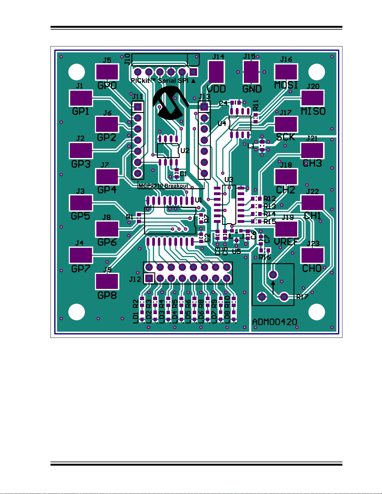
A.3.3 Board – Top Silk and Copper
Schematic and Layouts
© 2012 Microchip Technology Inc. DS52057A-page 29
Page 32

MCP2210 Evaluation Kit User’s Guide
A.3.4 Board – Top Copper
DS52057A-page 30 © 2012 Microchip Technology Inc.
Page 33
A.3.5 Board – Bottom Silk
Schematic and Layouts
© 2012 Microchip Technology Inc. DS52057A-page 31
Page 34

MCP2210 Evaluation Kit User’s Guide
A.3.6 Board – Bottom Silk and Copper
DS52057A-page 32 © 2012 Microchip Technology Inc.
Page 35

MCP2210 EVALUATIO N KI T
USER’S GUIDE
Appendix B. Bill of Mater ials
TABLE B-1: BILL OF MATERIALS - MCP2210 BREAKOUT BOARD
Qty Reference Description_ Manufacturer Part Number
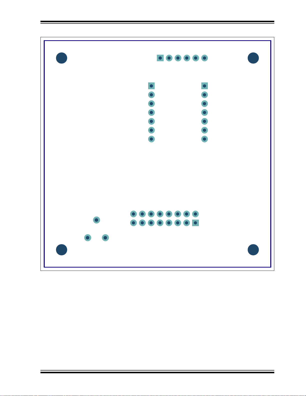
1 C1 Cap. Cer. 22 uF 10V 20% Y5V 1206 TDK
3 C2, C4, C5 Cap. Cer. 1 uF 10% 16V X7R 0603 AVX Corporation 0603YC104KAT2A
1 C3 Cap. Cer. 4.7 uF 6.3V 10% X5R 0603 TDK Corporation C1608X5R0J475K
1 C6 Cap. Cer. 1 uF 16V 10% X7R 0603 TDK Corporation C1608X7R1C105K
2J1, J2 DO NOT POPULATE
Conn. Hdr. Male .100 1x7 POS Vert.
1J3 DO NOT POPULATE
Conn. Hdr. Male .100 1x6 POS Vert.
1J4 DO NOT POPULATE
Conn. Hdr. Male .100 1x3 POS Vert.
1 J5 Conn. Rcpt. USB Mini B R/A SMD Hirose Electric Co. Ltd. UX60SC-MB-5ST(80)
1 PCB RoHS compliant bare PCB, MCP2210
Breakout Board
1 R1 Res. 390 Ohm 1/10W 5% 0603 SMD Panasonic
1 U1 IC USB-TO-SPI SSOP-20 Microchip Technology
1 U2 IC LDO Reg. 500 mA 3.3V SOT-223-3 Microchip Technology
1 X1 Cer. Resonator 12.0 MHz SMD Murata Electronics
Note 1: The components listed in this Bi ll of Material s ar e represe nta tive of th e PCB assembly. The released BOM
used in manufacturing uses all RoHS-compliant components.
®
Corporation
TE Connectivity Ltd. HDR M 1x7 Vertical
TE Connectivity Ltd. HDR M 1x6 Vertical
TE Connectivity Ltd. HDR M 1x3 Vertical
— 104-00419
Inc.
Inc.
®
- ECG ERJ-3GEYJ391V
®
C3216Y5V1A226Z
MCP2210-I/SS
MCP1825S-3302E/DB
CSTCE12M0G55-R0
TABLE B-2: BILL OF MATERIALS - MCP2210 SPI SLAVE MOTHERBOARD
Qty Reference Description_ Manufacturer Part Number
5 C1, C2, C3,
C4, C6
2 C5, C7 Cap. Cer. 4.7 uF 6.3V 10% X5R 0603 TDK Corporation C1608X5R0J475K
19 J1, J2, J3, J4,
J5, J6, J7, J8,
J9, J14, J15,
J16, J17, J18,
J19, J20, J21,
J22, J23
1 J10 Conn. Hdr. Male .100 1x6 Pos. RA TE Connectivity Ltd. HDR M 1x6 RA
2 J11, J13 Conn. Hdr. Male .100 1x7 Pos. Vert. TE Connectivity Ltd. HDR M 1x7 Vertical
1 J12 Conn. Hdr. Male .100 2x8 Pos. Vert. TE Connectivity Ltd. HDR M 2x8 Vertical
1 L1 Ferrite Chip 47 Ohms 500 mA 0603 Laird Technologies
Note 1: The components listed in thi s Bill of Material s are repr esent ative of the PCB assembly. The released BOM
used in manufacturing uses all RoHS-compliant components.
© 2012 Microchip Technology Inc. DS52057A-page 33
Cap. Cer. 0.1 uF 50V X7R 10% 0603 TDK Corporation C1608X7R1H104K
PC test point Tin SMD Harwin Plc. S1751-46R
®
LI0603E470R-10
Page 36

MCP2210 Evaluation Kit User’s Guide
TABLE B-2: BILL OF MATERIALS - MCP2210 SPI SLAVE MOTHERBOARD (CONTINUED)
Qty Reference Description_ Manufacturer Part Number
8 LD1, LD2,
LD3, LD4,
LD5, LD6,
LD7, LD8
1 PCB RoHS compliant bare PCB, MCP2210
13 R1, R2, R3,
R4, R5, R6,
R8, R9, R10,
R12, R13,
R14, R15
1 R7 Res. 10k Ohm 1/10W 5% 0603 SMD Panasonic - ECG ERJ-3GEYJ103V
1 R11 Res. 33k Ohm 1/10W 5% 0603 SMD Panasonic - ECG ERJ-3GEYJ333V
1 R16 Res. 10k Ohm 1/10W 1% 0603 SMD Panasonic - ECG ERJ-3EKF1002V
1 R17 Trimmer 10K OHM 0.5W TH Bourns
1 U1 IC I/O Expander SPI 8B SOIC-18 Microchip Technology
1 U2 IC EEPROM 2k Bit 10 MHz SOIC-8 Microchip Technology
1 U3 IC ADC 12 BIT 2.7V 4 Ch. SPI SOIC-14 Microchip Technology
1 U4 IC Sensor Thermal SPI 5V SOIC-8 Microchip Technology
1 U5 IC Volt. Ref. 2.5V SOT-23-3 Microchip Technology
Note 1: The components listed in thi s Bill of Material s are repr esent ativ e of the PCB assembl y. The released BOM
used in manufacturing uses all RoHS-compliant components.
LED Smartled Red 630 nm 0603 OSRAM Opto
Semiconductors
GmbH.
— 104-00420
SPI Slave Motherboard
Res. 1k Ohm 1/10W 1% 0603 SMD Panasonic - ECG ERJ-3EKF1001V
®
, Inc. 3386F-1-103TLF
Inc.
Inc.
Inc.
Inc.
Inc.
LS L29K-G1J2-1-0-2-R18-Z
MCP23S08-E/SO
25LC020A-I/SN
MCP3204T-CI/SL
TC77-5.0MOA
MCP1525T-I/TT
DS52057A-page 34 © 2012 Microchip Technology Inc.
Page 37

NOTES:
Bill of Materials
© 2012 Microchip Technology Inc. DS52057A-page 35
Page 38

Worldwide Sales and Service
AMERICAS
Corporate Office
2355 West Chandler Blvd.
Chandler, AZ 85224-6199
Tel: 480-792-7200
Fax: 480-792-7277
Technical Support:
http://www.microchip.com/
support
Web Address:
www.microchip.com
Atlanta
Duluth, GA
Tel: 678-957-9614
Fax: 678-957-1455
Boston
Westborough, MA
Tel: 774-760-0087
Fax: 774-760-0088
Chicago
Itasca, IL
Tel: 630-285-0071
Fax: 630-285-0075
Cleveland
Independence, OH
Tel: 216-447-0464
Fax: 216-447-0643
Dallas
Addison, TX
Tel: 972-818-7423
Fax: 972-818-2924
Detroit
Farmington Hills, MI
Tel: 248-538-2250
Fax: 248-538-2260
Indianapolis
Noblesville, IN
Tel: 317-773-8323
Fax: 317-773-5453
Los Angeles
Mission Viejo, CA
Tel: 949-462-9523
Fax: 949-462-9608
Santa Clara
Santa Clara, CA
Tel: 408-961-6444
Fax: 408-961-6445
Toronto
Mississauga, Ontario,
Canada
Tel: 905-673-0699
Fax: 905-673-6509
ASIA/PACIFIC
Asia Pacific Office
Suites 3707-14, 37th Floor
Tower 6, The Gateway
Harbour City, Kowloon
Hong Kong
Tel: 852-2401-1200
Fax: 852-2401-3431
Australia - Sydney
Tel: 61-2-9868-6733
Fax: 61-2-9868-6755
China - Beijing
Tel: 86-10-8569-7000
Fax: 86-10-8528-2104
China - Chengdu
Tel: 86-28-8665-5511
Fax: 86-28-8665-7889
China - Chongqing
Tel: 86-23-8980-9588
Fax: 86-23-8980-9500
China - Hangzhou
Tel: 86-571-2819-3187
Fax: 86-571-2819-3189
China - Hong Kong SAR
Tel: 852-2401-1200
Fax: 852-2401-3431
China - Nanjing
Tel: 86-25-8473-2460
Fax: 86-25-8473-2470
China - Qingdao
Tel: 86-532-8502-7355
Fax: 86-532-8502-7205
China - Shanghai
Tel: 86-21-5407-5533
Fax: 86-21-5407-5066
China - Shenyang
Tel: 86-24-2334-2829
Fax: 86-24-2334-2393
China - Shenzhen
Tel: 86-755-8203-2660
Fax: 86-755-8203-1760
China - Wuhan
Tel: 86-27-5980-5300
Fax: 86-27-5980-5118
China - Xian
Tel: 86-29-8833-7252
Fax: 86-29-8833-7256
China - Xiamen
Tel: 86-592-2388138
Fax: 86-592-2388130
China - Zhuhai
Tel: 86-756-3210040
Fax: 86-756-3210049
ASIA/PACIFIC
India - Bangalore
Tel: 91-80-3090-4444
Fax: 91-80-3090-4123
India - New Delhi
Tel: 91-11-4160-8631
Fax: 91-11-4160-8632
India - Pune
Tel: 91-20-2566-1512
Fax: 91-20-2566-1513
Japan - Osaka
Tel: 81-66-152-7160
Fax: 81-66-152-9310
Japan - Yokohama
Tel: 81-45-471- 6166
Fax: 81-45-471-6122
Korea - Daegu
Tel: 82-53-744-4301
Fax: 82-53-744-4302
Korea - Seoul
Tel: 82-2-554-7200
Fax: 82-2-558-5932 or
82-2-558-5934
Malaysia - Kuala Lumpur
Tel: 60-3-6201-9857
Fax: 60-3-6201-9859
Malaysia - Penang
Tel: 60-4-227-8870
Fax: 60-4-227-4068
Philippines - Manila
Tel: 63-2-634-9065
Fax: 63-2-634-9069
Singapore
Tel: 65-6334-8870
Fax: 65-6334-8850
Tai wan - Hsin Chu
Tel: 886-3-5778-366
Fax: 886-3-5770-955
Taiwan - Kaohsiung
Tel: 886-7-536-4818
Fax: 886-7-330-9305
Taiwan - Taipei
Tel: 886-2-2500-6610
Fax: 886-2-2508-0102
Thailand - Bangkok
Tel: 66-2-694-1351
Fax: 66-2-694-1350
EUROPE
Austria - Wels
Tel: 43-7242-2244-39
Fax: 43-7242-2244-393
Denmark - Copenhagen
Tel: 45-4450-2828
Fax: 45-4485-2829
France - Paris
Tel: 33-1-69-53-63-20
Fax: 33-1-69-30-90-79
Germany - Munich
Tel: 49-89-627-144-0
Fax: 49-89-627-144-44
Italy - Milan
Tel: 39-0331-742611
Fax: 39-0331-466781
Netherlands - Drunen
Tel: 31-416-690399
Fax: 31-416-690340
Spain - Madrid
Tel: 34-91-708-08-90
Fax: 34-91-708-08-91
UK - Wokingham
Tel: 44-118-921-5869
Fax: 44-118-921-5820
11/29/11
DS52057A-page 36 © 2012 Microchip Technology Inc.
 Loading...