

Page 1

MCP215X Data Logger
Demo Board
User’s Guide
2004 Microchip Technology Inc. DS51516A
Page 2
Note the following details of the code protection feature on Microchip devices:
• Microchip products meet the specification contained in their particular Microchip Data Sheet.
• Microchip believes that its family of products is one of the most secure families of its kind on the market today, when used in the
intended manner and under normal conditions.
• There are dishonest and possibly illegal methods used to breach the code protection feature. All of these methods, to our
knowledge, require using the Microchip products in a manner outside the operating specifications contained in Microchip’s Data
Sheets. Most likely, the person doing so is engaged in theft of intellectual property.
• Microchip is willing to work with the customer who is concerned about the integrity of their code.
• Neither Microchip nor any other semiconductor manufacturer can guarantee the security of their code. Code protection does not
mean that we are guaranteeing the product as “unbreakable.”
Code protection is constantly evolving. We at Microchip are committed to continuously improving the code protection features of our
products. Attempts to break Microchip’s code protection feature may be a violation of the Digit al Millennium Copyright Act. If suc h a c t s
allow unauthorized access to your software or other copyrighted work, you may have a right to sue for relief under that Act.
Information contained in this publication regarding device
applications and the like is provided only for your convenience
and may be superseded by updates. It is your responsibility to
ensure that your application meets with your specifications.
MICROCHIP MAKES NO REPRESENTATIONS OR WARRANTIES OF ANY KIND WHETHER EXPRESS OR IMPLIED,
WRITTEN OR ORAL, STATUTORY OR OTHERWISE,
RELATED TO THE INFORMATION, INCLUDING BUT NOT
LIMITED TO ITS CONDITION, QUALITY, PERFORMANCE,
MERCHANTABILITY OR FITNESS FOR PURPOSE.
Microchip disclaims all liability arising from this information and
its use. Use of M icrochip’s prod ucts as critical co mponents in
life support systems is not authorized except with express
written approval by Microchip. No licenses are conveyed,
implicitly or otherwise, under any Microchip intellectual property
rights.
Trademarks
The Microchip name and logo, the Microchip logo, Accuron,
dsPIC, K
EELOQ, microID, MPLAB, PIC, PICmicro,
PICSTART, PRO MATE, PowerSmart, rfPIC, and
SmartShunt are registered trademarks of Microchip
Technology Incorporated in the U.S.A. and other countries.
AmpLab, FilterLab, MXDEV, MXLAB, PICMASTER, SEEVAL,
SmartSensor and The Embedded Control Solutions Company
are registered trademarks of Microchip Technology
Incorporated in the U.S.A.
Analog-for-the-Digital Age, Application Maestro, dsPICDEM,
dsPICDEM.net, dsPICworks, ECAN, ECONOMONITOR,
FanSense, FlexROM, fuzzyLAB, In-Circuit Serial
Programming, ICSP, ICEPIC, Migratable Memory, MPASM,
MPLIB, MPLINK, MPSIM, PICkit, PICDEM, PICDEM.net,
PICLAB, PICtail, PowerCal, PowerInfo, PowerMate,
PowerTool, rfLAB, rfPICDEM, Select Mode, Sm art Serial,
SmartTel and Total Endurance are trademarks of Microchip
Technology Incorporated in the U.S.A. and other countries.
SQTP is a service mark of Microchip Technology Incorporated
in the U.S.A.
All other trademarks mentioned herein are property of their
respective companies.
© 2004, Microchip Technology Incorporated, Printed in the
U.S.A., All Rights Reserved.
Printed on recycled paper.
Microchip received ISO/TS-16949:2002 quality system certification for
its worldwide headquarters, design and wafer fabrication facilities in
Chandler and Tempe, Arizona and Mountain View, California in
October 2003. The Company’s quality system processes and
procedures are for its PICmicro
devices, Serial EEPROMs, microperipherals, nonvolatile memory and
analog products. In addition, Microchip’s quality system for the design
and manufacture of development systems is ISO 9001:2000 certified.
®
8-bit MCUs, KEELOQ
®
code hopping
DS51516A-page ii 2004 Microchip Technology Inc.
Page 3

MCP215X DATA LOGGER
DEMO BOARD USER’S GUIDE
Tabl e of Contents
Preface ...........................................................................................................................1
Chapter 1. Overview.......................................................................................................7
1.1 Introduction .....................................................................................................7
1.2 What is the MCP215X Data Logger Demo Board? ........................................ 7
1.3 What the MCP215X Data Logger Demo Board Kit Includes .................... ...... 7
Chapter 2. Installation and Operation..........................................................................9
2.1 Introduction .....................................................................................................9
2.2 Features ................... .. .. ............. .. ........................... .. ........................... .. ....... 10
2.3 Getting St a rt ed ...... .............. .. .. ............. .. ........................... .. ......................... 11
2.4 Running th e d emos ............. .. .. ............. .. ........................... .. ......................... 23
2.5 MCP215X Data Logger Demo Board Description ........................................39
Appendix A. Schematic and Layouts ........................................................................45
A.1 Introduction ..................................................................................................45
A.2 Schematics and PCB Layout .......................................................................45
Appendix B. Bill-Of-Materials (BOM) .........................................................................49
Appendix C. MCP215X Connection Sequence Overview ........................................51
Appendix D. MCP215X 250-byte Data Transmit Table .............................................53
Worldwide Sales and Service ....................................................................................54
2004 Microchip Technology Inc. DS51516A-page iii
Page 4

MCP215X Data Logger Demo Board User’s Guide
NOTES:
DS51516A-page iv 2004 Microchip Technology Inc.
Page 5

MCP215X DATA LOGGER
DEMO BOARD USER’S GUIDE
Preface
NOTICE TO CUSTOMERS
All documentation becomes dated, and this manual is no exception. Microchip tools
and documentation are constantly evolving to meet customer needs, so some actual
dialogs and/or tool descriptions may dif fer from those in this document. Please refer
to our web site (www.microchip.com) to obt ain the latest documentation available.
Documents are identified with a “DS” number. This number is located on the bottom
of each page, in front of the page number. The numbering convention for the DS
number is “DSXXXXXA”, where “XXXXX” is the document number and “A” is the
revision level of the document.
For the most up-to-date information on development tools, see the MPLAB
on-line help. Select the Help menu, and then Topics to open a list of available on-line
help files.
®
IDE
INTRODUCTION
This chapter contains general information that will be useful to know before using the
MCP215X Data Logger Demo Board User’s Guide. Items discussed in this chapter
include:
• About This Guide
• Recommended Reading
• The Microchip Web Site
• Customer Support
2004 Microchip Technology Inc. DS51516A-page 1
Page 6

MCP215X Data Logger Demo Board User’s Guide
ABOUT THIS GUIDE
Document Layout
This document describes how to use the MCP215X Data Logger Demo Board User’s
Guide as a development tool to emulate and debug firmware on a target board. The
manual layout is as follows:
• Chapter 1: Product Overv iew – Important information about the MCP215X Data
Logger Demo Board User’s Guide.
• Chapter 2: MCP215X Data Logger Demo Board User’s Guide – Includes
instructions on how to get started with this demo board, with a detailed description
of each function.
• Appendix A: Schematic and Layouts – Shows the schematic and layout
diagrams for the MCP215X Data Logger Demo Board.
• Appendix B: Bill-of-Materials – Lists the parts used to build the MCP215X Data
Logger Demo Board.
• Appendix C: Connection Sequence – Shows the connection sequence between
a Primary device and the MCP215X (Secondary device). This connection
sequence is shown at an overview level and does not show exact operation.
• Appendix D: 250 Byte Transmit Table – Shows the data that is transmitted by
the program when in 250-Byte Transmit mode.
DS51516A-page 2 2004 Microchip Technology Inc.
Page 7
Preface
Conventions Used in this Guide
This manual uses the following docum entation conventions:
DOCUMENTATION CONVENTIONS
Description Represents Examples
Arial font:
Italic charac ters Referenced books MPLAB
Emphasized text ...is the only compiler...
Initial caps A window the Output window
A dialog the Settings dialog
A menu selection select Enable Programmer
Quotes A field name in a window or
dialog
Underlined, italic text with
right angle bracket
Bold characters A dialog button Click OK
‘bnnnn A binary number where n is a
Text in angle brackets < > A key on the keyboard Press <Enter>, <F1>
Courier font:
Plain Courier Sample source code #define START
Italic Courier A variable argument file.o, where file can be
0xnnnn A hexadecimal number whe re
Square brackets [ ] Optional arguments mcc18 [options] file
Curly brackets and pipe
character: { | }
Ellipses... Replaces repeated text var_name [,
A menu path File>Save
A tab Click the Power tab
digit
Filenames autoexec.bat
File paths c:\mcc18\h
Keywords _asm, _endasm, static
Command-line options -Opa+, -Opa-
Bit values 0, 1
n is a hexadecimal digit
Choice of mut ually exclu s ive
arguments; an OR selection
Represents code supplied by
user
“Save project before build”
‘b00100, ‘b10
any valid filename
0xFFFF, 0x007A
[options]
errorlevel {0|1}
var_name...]
void main (void)
{ ...
}
®
IDE User’s Guide
2004 Microchip Technology Inc. DS51516A-page 3
Page 8

MCP215X Data Logger Demo Board User’s Guide
RECOMMENDED READING
This user's guide describes how to use MCP215X Data Logger Demo Board User’s
Guide. Other useful documents are listed below. The following Microchip documents
are available and recommended as supplemental reference resources.
MCP2150 Data Sheet (DS21790)
This data sheet provides detailed information regarding the MCP2150 device.
MCP2155 Data Sheet (DS21790)
This data sheet provides detailed information regarding the MCP2155 device.
AN858, “Interfacing the MCP215x to Host Controller” (DS00858)
This application note discusses the interface between a Host Controller and the
MCP215X device.
AN888, “Programming the Palm OS
This application note discusses the programming of a Palm™ PDA to interface to an
®
standard device using IrCOMM.
IrDA
AN926, “Programming the Pocket PC OS for Embedded IR Applications”
(DS00926)
This application note discusses the programming of a Pocket PC PDA to interface to
an IrDA standard device using IrCOMM.
AN941, “Programming Windows
This application note discusses the programming of a Windows XP PC to interface to
an IrDA standard device using IrCOMM.
®
for Embedded IR Applications” (DS00888)
®
XP for Embedded IR Applications” (DS00941)
DS51516A-page 4 2004 Microchip Technology Inc.
Page 9

THE MICROCHIP WEB SITE
Microchip provides online support via our web site at www.microchip.com. This web
site is used as a means to make files and information easily available to customers.
Accessible by using your favorite Internet browser, the web site contains the following
information:
• Product Support – Data sheets and errata, application notes and sample
programs, design resources, user’s guides and hardware support documents,
latest software releases and archived software
• General Technical Support – Frequently Asked Questions (FAQ), technical
support requests, online discussion groups, Microchip consultant program
member listing
• Business of Microchip – Product selector and ordering guides, latest Microchip
press releases, listing of seminars and events, listings of Microchip sales offices,
distributors and factory representatives
CUSTOMER SUPPORT
Users of Microchip products can receive assistance through several channels:
• Distributor or Representative
• Local Sales Office
• Field Application Engineer (FAE)
• Technical Support
• Development Systems Information Line
Customers should contact their distributor, representative or field application engineer
(FAE) for support. Local sales offices are also available to help customers. A listing of
sales offices and locations is included in the back of this document.
Technical support is available through the web site at: http://support.microchip.com
In addition, there is a Development Systems Information Line which lists the latest
versions of Microchip's development systems software products. This line also
provides information on how customers can receive currently available upgrade kits.
The Development Systems Information Line numbers are:
1-800-755-2345 – United States and most of Canada
1-480-792-7302 – Other Internatio nal Loca tio ns
Preface
2004 Microchip Technology Inc. DS51516A-page 5
Page 10

MCP215X Data Logger Demo Board User’s Guide
NOTES:
DS51516A-page 6 2004 Microchip Technology Inc.
Page 11

MCP215X DATA LOGGER
DEMO BOARD USER’S GUIDE
Chapter 1. Overview
1.1 INTRODUCTION
This chapter provides an overview of the MCP215X Data Logger Demo Board and
covers the following topics:
• What is the MCP215X Data Logger Demo Board?
• What the MCP215X Data Logger Demo Board kit includes
1.2 WHAT IS THE MCP215X DATA LOGGER DEMO BOARD?
The MCP215X IrDA® Standard Protocol Stack Controller device allows the system
designer to implement a low-cost, wireless IR port in any application providing support
for the IrDA standard protocol stack and IrDA standard bit encoding/decoding.
The MCP215X Data Logger Demo Board is used to evaluate and demonstrate either
the MCP2150 or MCP2155 device in a data-logging application. The board will
communicate to a Primary device (such as a PDA (e.g., Palm™ or Pocket PC) or laptop
computer). It is intended to serve as an example to assist system designers in
developing an IrDA standard node using the MCP215X device.
Though the MCP215X Data Logger Demo Board ships with a MCP2150 installed, this
device may be interchanged with a MCP2155, allowing the MCP2155 to be evaluated.
Note: If the MCP2150 is repl ace d by the MC P21 55 , the MC P2 15 5 dev ice mu st
have the firmware programmed into the device. Ensure that the demo
program firmware was assembled for the MCP2155 (the demo program uses
conditional assemb ly to use t he same sou r ce file for th e t wo devic es) . Th e
“MCP215X” varia ble needs to be equat ed to ‘55 ’. The MPASM™ assemb ler
will display a message as to which de vice the fil e has assemble d for.
1.3 WHAT THE MCP215X DATA LOGGER DEMO BOARD KIT INCLUDES
This MCP215X Data Logger Demo Board Kit includes:
• The MCP215X Data Logger Demo Board (with MCP2150 installed)
• MCP215X Data Logger Demo Board User’s Guide (on CD-ROM)
• CD-ROM also includes:
- Palm PDA Primary device application program
(and related Application Note 888)
- Pocket PC Primary device application program
(and related Application Note 926)
- Windows XP Primary device application program
(and related Application Note 941)
- Demo board firmware that can be conditionally assembled for either the
MCP2150 or the MCP2155.
2004 Microchip Technology Inc. DS51516A-page 7
Page 12

MCP215X Data Logger Demo Board User’s Guide
NOTES:
DS51516A-page 8 2004 Microchip Technology Inc.
Page 13

Chapter 2. Installation and Operation
2.1 INTRODUCTION
This chapter discusses the installation and operation of the MCP215X Data Logger
Demo Board and a Primary device for data communication. This demonstrates an IrDA
standard system and will assist the system designer on how to integrate an IR port into
a system.
The MCP215X Data Logger Demo Board demonstrates the implementation of an
embedded system with an IrDA standard interface. This system operates as an IrDA
standard Secondary device using either the MCP2150 or the MCP2155 device.
The IrDA standard system requires the Primary device to be running an appropriate
application program. The MCP215X Data Logger Demo Board interfaces to the
Primary device application programs that are currently available from Microchip. The
three application programs available for the following Primary device systems are:
•Palm OS
•Microsoft® Pocket PC 2003
•Microsoft
These application programs are supported by three application notes that discuss the
programming of these particular operating systems. These application notes are:
• AN888, “Programming the Palm OS
• AN926, “Programming the Pocket PC for Embedded IR Applications”, DS00926
• AN941, “Programming Windows XP
®
®
Windows XP
MCP215X DATA LOGGER
DEMO BOARD USER’S GUIDE
®
for Embedded IR Applications”, DS00888
®
for Embedded IR Applications”, DS00941
Note: References to a MCP215X device in this document can refer to either the
MCP2150 or the MCP2155 device.
The host UART interface includes non-data flow control signals. These are the signals
between a Host Controller and a MCP215X device. A discussion of the host UART
interface is given in the following application note:
• AN858, “Interfacing the MCP215X to a Host Controller”, DS00858
2004 Microchip Technology Inc. DS51516A-page 9
Page 14

MCP215X Data Logger Demo Board User’s Guide
2.2 FEATURES
The MCP215X Data Logger Demo Board has the following features:
• Communicates directly to Primary device (PDA or laptop computer) running the
supplied Primary device application program or running a terminal emulation
program
• LCD display (2 row x 16 character) for display of system information
• Data is transmitted in an easy-to-read format
• Reprogrammable PIC16F877 with MPLAB
for user application development
• 18-pin socket for the installation of either a MCP2150 (default device) or a
MCP2155 (optional device)
• Header that allows either several board signals to be monitored or allows the
MCP215X Data Logger Demo Board to be interfaced to the user’s system
• Eight LEDs that indicate MCP215X status (CTS, RTS, DTR, DSR, CD and RI
activity)
• Eight LEDs that are connected to PORTD of the PIC16F877
• Battery-operated by a 9V source (can use a 9V battery)
•PICmicro
• Two switches (SW2 and SW3) to control the PICmicro MCU program operation
• Header and jumpers to allow the electrical removal of the optical transceiver and
the installation of an alternate optical transceiver circuit (on a daughter board)
• Variable resistor connected to PICmicro MCU A/D input
• 8-pin DIP socket for the installation of an optional serial EEPROM (24LC256)
®
microcontroller (MCU) RESET switch
®
In-Circuit Debugger (ICD) interface
DS51516A-page 10 2004 Microchip Technology Inc.
Page 15
2.3 GETTING STARTED
This section presents an overview of the following system blocks:
• The MCP215X Data Logger Demo Board Hardware
• The MCP215X Data Logger Demo Board Firmware
• The Primary device Graphical User Interface (GUI)
This should give you an understanding of what these components do in the complete
IrDA standard system.
2.3.1 The MCP215X Data Logger Demo Board Hardware Overview
The major components for the MCP215X Data Logger Demo Board are:
1. MCP215X device (U3)
2. Optical transceiver (U5 - TFDS 4500)
3. PICmicro MCU (U1 - PIC16F877)
4. LCD module
5. Power supply
6. User inputs to PICmicro MCU (SW2, SW3 and variable resistor (VR1))
7. PICmicro MCU RESET
8. PICmicro MCU crystal (Y2)
The MCP215X Data Logger Demo Board is fully assembled and tested for evaluation
and demonstration of the MCP2150 or MCP2155 features. A block diagram of the
demo board is shown in Figure 2-1. The board has been designed to allow the installation of an optional LCD contrast control (VR2) and serial EEPROM device. These
optional components are removed from the MCP215X Data Logger Demo Board block
diagrams for readability.
For more detailed circuit information, refer to Appendix A. “Schematic and Layouts”
and Appendix B. “Bill-Of-M at erials (BOM) ” .
Installation and Operation
FIGURE 2-1: MCP215X DATA LOGGER DEMO BOARD BLOCK DIAGRAM
Power
ICD
SW3
SW2
RESET
VR1
9V Battery
Power LED
Power Supply
3
PICmicro
MCU
(40-pin)
U1
MCP215X Header
J4
®
Optional
Not
Installed
VR2
Optional
Not
Installed
SEE
U2
LCD Module
(2 Line x 16 Character)
RD7
CTS RTS CD DSR
TX RX RI DTR
JP3
Encoder/Decoder
MCP215X
U3
JP5
JP6
JP2
JP1
RD0
JP4
JP7
Discrete
Transceiver
Header 1
J1
U5
J5
Header 2
2004 Microchip Technology Inc. DS51516A-page 11
Page 16

MCP215X Data Logger Demo Board User’s Guide
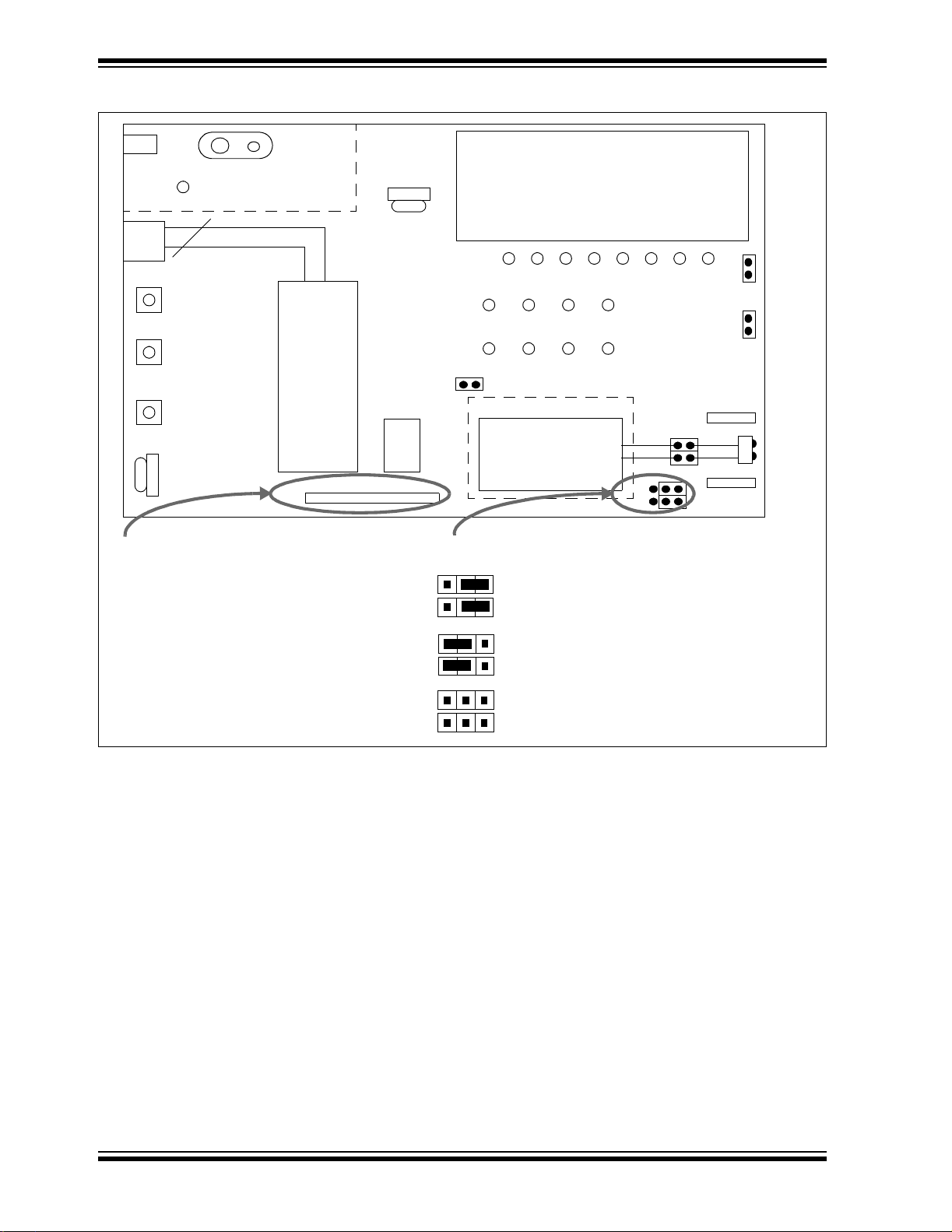
Figure 2-2 shows the layout of the MCP215X Data Logger Demo Board with indication
to points of interest.
FIGURE 2-2: MCP215X DATA LOGGER DEMO BOARD
9V Battery
Power
Power LED
Power Supply
SW3
SW2
RESET
3
PICmicro
(40-pin)
J4
®
MCU
U1
MCP215X Header
ICD
VR1
Switches for program selection and
program state
SW3 SW2
— — Waiting for program selection
— D Vending machine
D — Not used
D D 250-byte S→P data transfer
Reset Switch
— PICmicro MCU in normal operation
D PICmicro MCU in RESET state
LCD Module
(2 Line x 16 Character)
RD7
CTS RTS CD DSR
TX RX RI DTR
JP3
Encoder/Decoder
MCP215X
Connect/Isolate
TFDS 4500 TXD and RXD pins
TFDS 4500 TXD and RXD
Connected to MCP215x
TFDS 4500 TXD and RXD
NOT Connected to MCP215x
(Header 1 and 2 can be used)
JP2
U3
JP1
JP5
JP6
Ground/Float
PORTD LEDs Cathode
LED Cathode
Grounded
LED Cathode
Floating
(LEDs will not
illuminate)
RD0
JP4
JP7
Discrete
Transceiver
Header 1
J1
U5
J5
Header 2
DS51516A-page 12 2004 Microchip Technology Inc.
Page 17
Figure 2-3 shows the switches used to reset the MCP2150 and select one of two demo
programs. Switch RESET resets the MCP2150 and switch S2 is used for program
selection.
FIGURE 2-3: MCP215X DATA LOGGER DEMO BOARD
Installation and Operation
Power
Power LED
ICD
VR1
MCP215X Enable
3
SW3
SW2
RESET
MCP215X Enabled
(Normal Operation)
MCP215X in low-power state
9V Battery
Power Supply
PICmicro
MCU
(40-pin)
U1
MCP215X Header
J4
LCD Module
(2 Line x 16 Character)
RD7
®
CTS RTS CD DSR
TX RX RI DTR
JP3
Encoder / Decoder
JP2
MCP215X
Header 1 and Header 2
allow connection to a daughter
board for implementation of other
optical transceiver circuits
VDD
J1
VSS
VDD
J5
VSS
RXIR
TXIR
RXPD
RXPDREF
U3
JP1
JP5
JP6
Power/Isolate
Integrated Transceiver
RD0
JP4
JP7
Discrete
Transceiver
Header 1
J1
U5
J5
Header 2
TFDS 4500
is Powered
TFDS 4500
is NOT powered
(Header 1 and 2
can be used)
2004 Microchip Technology Inc. DS51516A-page 13
Page 18
MCP215X Data Logger Demo Board User’s Guide
FIGURE 2-4: MCP215X DATA LOGGER DEMO BOARD
9V Battery
Power
Power LED
Power Supply
ICD
VR1
MCP215X Demo Board Signal Header
Note: Actual silk-screen placement for the
3
PICmicro
SW3
SW2
RESET
RTS and CTS labels should be switched
MCU
(40-pin)
U1
MCP215X Header
J4
®
VR2
SEE
U2
LCD Module
(2 Line x 16 Character)
RD7
CTS RTS CD DSR
TX RX RI DTR
JP3
Encoder/Decoder
JP2
MCP215X
U3
Optional MCP215X BAUD1:BAUD0 pin pull-up/pull-down
selection
MCP215X BAUD1:BAUD0 pins are pulled up
JP1
JP5
JP6
RD0
JP4
JP7
Discrete
Transceiver
Header 1
J1
U5
J5
Header 2
MCP215X BAUD1:BAUD0 pins are pulled down
MCP215X BAUD1:BAUD0 pins are controlled
by PIC16F877 I/O pins
(R37 and R38 must be installed)
DS51516A-page 14 2004 Microchip Technology Inc.
Page 19

Installation and Operation
A description of the MCP215X Data Logger Demo Board jumpers is given in Table 2-1.
TABLE 2-1: JUMPER DESCRIPTIONS AND SETTINGS
Jumper #Typical
Settings
JP1 S To connect TXIR of MCP2150 to TXD of U5 (TFDS 4500)
JP2 S To connect RXIR of MCP2150 to RXD of U5 (TFDS 4500)
JP3 O To connect EN of MCP2150 to V
JP4 S To connect cathode of LEDs (RD7:RD0) to VSS
JP5 N/A To control source of MCP2150 BAUD1 pin
JP6 N/A To control source of MCP2150 BAUD0 pin
JP7 S To connect VDD to integrated optical transceiver (U5) - TFDS
Legend: S = Jumper is shorted (Closed) O = Jumper is Open
Note 1: This is the jumper settings for using the integrated transceiver where the PIC16F877 controls the baud
rate and the PORTD LEDs are used.
(1)
S = TXIR connected to TXD
O = TXIR Not connected to TXD
S = RXIR connected to RXD
O = RXIR Not connected to RXD
S = MCP2150 in Low-power mode
O = MCP2150 during normal operation
S = Cathode of LEDs to V
O = Cathode of LEDs floating
4500
Description Comment
When Open, the signal can
come from the daughter
board connected to Header
J1/J5.
When Open, the signal can
come from the daughter
board connected to Header
J1/J5.
SS
The PCB default state is
SS
shorted between jum per . No
jumper is required.
2004 Microchip Technology Inc. DS51516A-page 15
Page 20

MCP215X Data Logger Demo Board User’s Guide
2.3.2 The Embedded System Firmware Overview
There are two PIC16F877 firmware programs that can be demonstrated on the demo
board. These are:
• A vending machine that allows the uploading of data and responds to the
commands of the Primary device
• A 250-byte secondary device (S) to primary device (P) data transfer. This
demonstrates the S → P data throughput
The 250-byte Secondary device (S) to Primary device (P) data transfer program has
two options. These are:
1. Transfer data from the Host Controller (PIC16F877) to the MCP2150 while the
CTS signal is low.
2. Transfer 64 bytes of data from the Host Controller (PIC16F877) to the MCP2150
after CTS signal falling edge.
Option 2 will demonstrate higher S → P data throughput.
Typical Primary devices include Palm or Pocket PC PDAs and laptop PCs with an IrDA
standard infrared port. The embedded system acts as an IrDA standard Secondary
device.
The PIC16F877 firmware follows the flow control of the host UART interface. These are
the signals between a Host Controller and a MCP2150 device.
The details of the vending machine firmware operation are discussed in
Section 2.3.2.1 “Vending Machine Program Description”.
The details of the “250 byte Secondary Device (S) to Primary Device (P) Data Transfer”
firmware operation are discussed in Section 2.3.2.2 “250-byte Secondary Device (S)
to Primary Device Data Transfer Program Description”.
Figure 2-5 shows the program flow that occurs to select between these two programs.
The MCP215X Data Logger Demo Board LCD module will display information on the
state of the firmware execution. This information includes queries for user input.
The selection of the program is dependant on the switches (SW2 and SW3) that are
depressed (see Figure 2-4).
TABLE 2-2: DEMO PROGRAM SELECTION
SW3 SW2 Demo Program
——N/A
(waiting for a switch to be depressed)
— D Vending machine
D — Not implemented
DDS→P Transfer 250-bytes from demo board to Primary device (PDA)
Note: D = Depressed — = Not depressed
The MCP2150/MCP2155 source code of the MCP215X Data Logger Demo Board is
available for download from the Microchip web site at www.microchip.com. This board
also supports the MCP2155 device with only a change of the PIC16F877 firmware. The
MCP2140 can be supported with some hardware modifications and changes to the
PIC16F877 firmware.
DS51516A-page 16 2004 Microchip Technology Inc.
Page 21

Installation and Operation
FIGURE 2-5: PIC16F877 FIRMWARE FLOW - MAIN
RESET
Display Firmware
Revision Information
Display
Program Selection
Switch
SW3
SW2 or
SW2+SW3
Depressed?
SW2
SW2+SW3
Display Vending
Machine Program Selected
Vending Machine Routine
Display 250-byte S->P
Transfer Program Selected
250-byte S->P Transfer Routine
2004 Microchip Technology Inc. DS51516A-page 17
Page 22

MCP215X Data Logger Demo Board User’s Guide
2.3.2.1 VENDING MACHINE PROGRAM DESCRIPTION
This demo emulates a vending machine by counting the number of each item (soda
and candy) dispensed.
Once the MCP215X Data Logger Demo Board has completed reset and the LCD
module indicates which switches to depress to select a program, depress switch S2.
The LCD module will indicate that the vending machine program is selected.
The LCD module will then indicate the values of the soda and candy counters.
Depressing the S2 switch will increment the soda counter, while depressing the S3
switch will increment the candy counter. Once either switch is depressed, the LCD
module displays the new counter values. Each counter is an 8-bit value and can display
a value from 0 to 255 (decimal).
When the PIC16F877 receives a data byte, the value is checked to determine the
operation to perform. The vending machine program understands two commands:
1. Transmit the counter values.
2. Clear the counter values.
Table 2-3 shows the two commands that the vending machine program accepts. All
other data values that are received are ignored. Once the program has received the
“Transmit the current counter values” command, the PIC16F877 will transmit the data
on two lines, in the following easy-to-read format:
Soda = xxx
Candy = xxx
where xxx is the counter value
TABLE 2-3: VENDING MACHINE COMMANDS
Description
Transmit the current soda and candy counter values to the
Primary device
Clear the current soda and candy counters 6 0x36
ASCII Code Hex Code
Command
5 0x35
Note: All other received data values are ignored.
The host UART interface is operating at 115,200 baud.
The transfer will not commence until the PIC16F877 has received a data byte from the
Primary device.
The PIC16F877 follows the flow control of the MCP2150 to ensure that data is not lost.
The MCP2150 handles all the IrCOMM protocol for the data packets that it receives
from the PIC16F877.
Once the command has been processed, the PIC16F877 waits for the next command
to be received.
The program flow for the vending machine demo is shown in Figure 2-6.
DS51516A-page 18 2004 Microchip Technology Inc.
Page 23

Installation and Operation
FIGURE 2-6: PIC16F877 FIRMWARE FLOW - VENDING MACHINE
Vending Machine Routine
Display Soda and
Candy Information
Switch
SW2 or SW3
Depressed?
No
Data
Byte
Received from
Primary
Device?
No
Yes
Yes
Data
Byte
= 0x35?
No
Which
Switch is
Depressed?
SW2
Increment Soda Counter
Yes
SW3
Increment Candy Counter
Transmit Data to
Primary Device
Data
Byte
= 0x36?
No
2004 Microchip Technology Inc. DS51516A-page 19
Yes
Clear Soda and Candy
Counter Values
Page 24

MCP215X Data Logger Demo Board User’s Guide
2.3.2.2 250-BYTE SECONDARY DEVICE (S) TO PRIMARY DEVICE DATA
TRANSFER PROGRAM DESCRIPTION
After the MCP215X Data Logger Demo Board has completed reset and the LCD module indicates which switches to depress to select a program, depress switches S2 and
S3 simultaneously. The LCD module will indicate that the 250-byte S→P program is
selected.
You then need to specify the data transfer method. The host UART interface is
operating at 115,200 baud. There are two methods by which to accomplish this.
In the first method, the PIC16F877 will transfer data to the MCP2150 while the CTS
signal is low. This is the easiest method to implement. To select this method, depress
switch S2. After depressing S2, the LCD will indicate the mode of data transfer and that
it is waiting. The transfer will not commence until the PIC16F877 has received a data
byte from the Primary device.
In the second method, the PIC16F877 will transfer 64 bytes of the data table to the
MCP2150 after the falling edge of the CTS signal. This method gives the best data
throughput. T o select this method, depress switch S3. After depressing S3, the LCD will
indicate the mode of data transfer and that it is waiting. The transfer will not commence
until the PIC16F877 has received a data byte from the Primary device.
The PIC16F877 follows the flow control of the MCP2150 to ensure that data is not lost.
The MCP2150 handles all the IrCOMM protocol for the data packets that it receives
from the PIC16F877.
After the table has completed transmission, the PIC16F877 returns to the routine that
asks for the data transfer method.
The program flow for the “250 Byte Secondary Device (S) to Primary Device (P) Data
Transfer” demo is shown in Figure 2-7.
The 250-byte data table transmitted from the MCP215X Data Logger Demo Board to
the Primary device is shown in Appendix D. “MCP215X 250-Byte Data Transmit
Table”. These values will be displayed in the Primary device’s terminal emulation
program window.
Note: The byte sent by the Primary device is expected since most PDAs will not
establish a link until data is sent.
Depending on the PDA application program used (Palm™ or Pocket PC),
the operation of the Connect button varies.
The PIC16F877 receives a single byte from the IrDA standard Primary device and then
a 250-byte table is transmitted back to the Primary device.
If you desire more than 250 bytes to be transferred, the source code is written to allow
this 250-byte table to be transmitted multiple times. At the beginning of the S→P Data
Transfer routine (routine has label S2Pxfer), there is a #define for the TableCNTR.
This is set to ‘1’, but can be changed to allow the data table to be transmitted
“TableCNTR” time. TableCNTR should not be greater than D’255’ (8-bit value)
DS51516A-page 20 2004 Microchip Technology Inc.
Page 25

Installation and Operation
FIGURE 2-7: PIC16F877 FIRMWARE FLOW - 250-BYTE S->P TRANSFER
250-Byte S->P Transfer Routine
Display S->P Transfer
Method Selection
Switch
SW2 or SW3
Depressed?
SW3
Display Xfer 64B/Window
Waiting Message
Data
Byte
Received from
Primary
Device?
No
SW2
Yes
Transfer Table Using
64B/Window Method
Display Xfer if CTS Low
Waiting Message
Data
Byte
Received from
Primary
Device?
No
Yes
Transfer Table Using
CTS Low Method
2004 Microchip Technology Inc. DS51516A-page 21
Page 26

MCP215X Data Logger Demo Board User’s Guide
2.3.3 The Primary Device Graphical User Interface (GUI) Overview
Three Primary device platforms have had application programs developed to interface
to the MCP215X Data Logger Demo Board. These platforms are:
•Palm PDAs
• Pocket PC PDAs
• Window XP PCs
The GUI for these three platforms have been designed to look similar. Figure 2-8
shows the GUIs for the three platforms. A more detailed description of each GUI is
given in the section that describes how to use that Primary device with the MCP215X
Data Logger Demo Board (Section 2.4.1 “Running the MCP215X Data Logger
Demo Board with a Palm PDA”, Section 2.4.2 “Running the MCP215X Data Logger Demo Board with a Pocket PC PDA” or Section 2.4.3 “Running the MCP215X
Data Logger Demo Board with a Window XP PC with an IrDA Standard Port”).
FIGURE 2-8: PRIMARY DEVICE GUIS
Palm™ PDA Pocket PC PDA Windows® XP PC
DS51516A-page 22 2004 Microchip Technology Inc.
Page 27

2.4 RUNNING THE DEMOS
This demo board can interface to any Primary device that implements the IrCOMM
9-wire “cooked” protocol layer. Some typical Primary devices include:
1. Palm PDA
2. Pocket PC PDA
3. Laptop PC with IrDA Standard Port
Three application programs have been developed to interface these devices to the
MCP215X Data Logger Demo Board. One for each Primary device platform shown.
These application programs also have an associated application note to discuss the
implementation of the application program. These programs are discussed in the
following application notes:
• For Palm OS - Application Note 888, “Programming the Palm OS
IR Applications”, DS00888
• For Pocket PC OS - Application Note 926, “Programming the Pocket PC OS for
Embedded IR Applications”, DS00926
• For Windows XP - Application Note 941, “Prog ra mmi ng Windows
Embedded IR Applications”, DS00941
Other third-party programs may be used to communicate with the MCP215X Data Logger
Demo Board, though these methods will not be discussed in this document. If additional
information is desired, refer to the MCP2140 IrDA
Sensor Demo Bo ar d Use r’s Guid e ( DS5 14 87 ).
Installation and Operation
®
for Embedded
®
XP for
®
St an da rd Wir ele ss Te mper a tur e
2004 Microchip Technology Inc. DS51516A-page 23
Page 28

MCP215X Data Logger Demo Board User’s Guide
2.4.1 Running the MCP215X Data Logger Demo Board with a Palm
PDA
An overview of the Application Note 941 GUI is given (Section 2.4.1.1 “The Palm PDA
GUI”), followed by the operation of the demos (Section 2.4.3.2 “Running The Demos
Using The Application Note 941 Program”).
2.4.1.1 THE PALM PDA GUI
The GUI consists of a number of user-interface elements, including command buttons,
text labels and a text-entry field. Refer to Figure 2-9.
FIGURE 2-9: PALM PDA MAIN FORM
2
1
3
4
5
6
7
Send File
9
8
1. The Connect button attempts to establish a connection to the MCP215X Data
Logger Demo Board, with the Palm PDA acting as the Primary device. The label
to the left of the button provides an indication of the connection.
2. The Read Data button sends a query to the demo board, requesting the soda
and candy counter values. Received data is parsed and displayed.
3. The Clear Data button sends a command to the demo board, instructing it to
reset the application level counters. The command to “Read Data” is then sent to
ensure that the registers were cleared.
4. The ASCII/HEX button toggles the application between ASCII and HEX modes.
This value is used when preparing and transmitting data to the IR demo board.
This is useful when there is a need to send a non-printable value, such as
low-order ASCII. For example, to send the value 0x03, use the keyboard or
®
Graffiti
to enter “03” (without the quotes). This will be converted to 0x03 and
transmitted.
5. The Send button sends the data shown on the “TX Data” line. If HEX mode is
selected, minimal error-checking is performed.
6. The Show button causes a message box to be displayed that contains the
received buffer information.
7. The Reset button clears the Palm PDA application's receive data buffer.
8. The Send File button is used to send a file.
9. The 123 and ABC button opens a keyboard for data entry. The 123 button will
open the numeric keyboard, while the ABC button will open the alpha keyboard.
DS51516A-page 24 2004 Microchip Technology Inc.
Page 29

2.4.1.2 RUNNING THE DEMO USING THE APPLICATION NOTE AN888
PROGRAM
After saving the AN888 application program to your PC’s hard drive, the PC can communicate with the MCP215X Data Logger Demo Board. Section 2.4.1.2.1 “Steps to
Operate the Vendi ng Machine Demo” discusses how to operate the vending
machine program, while Section 2.4.1.2.2 “Steps to Operate the 250-byte S -> P
Data T r ansfer De mo” discusses how to operate the 250-byte Secondary device (S) to
Primary device (P) data transfer program.
2.4.1.2.1 Steps to Operate the Vending Machi ne Demo
The vending machine demo is shown by following the steps in Table 2-4.
TABLE 2-4: VENDING MACHINE DEMO - PALM™ PDA
Step Action Result
1 Pla ce both devi ces on a flat surfa ce about 25 cm (10”)
apart, and with the IR ports facing each other
2 On the MCP215X Data Logger Demo Board:
Ensure that jumpers JP1 and JP2 are shorted
(closed position).
3 On the MCP215X Data Logger Demo Board:
Ensure that jumper JP7 is shorted (closed position).
4 On the MCP215X Data Logger Demo Board:
Insert the 9V battery into the battery holder (BT1) or
plug a 9V AC to DC power supply (such as those
supplied with some Micr oc hip d eve lopment tools) into
the 9V DC connection plug (J2).
You may need to depress the RESET switch if the
LCD does not display the Microchip program revision
information and then the directions for demo program
selection.
5 On the MCP215X Data Logger Demo Board:
Depress Switch 2 (SW2).
6 On the PDA:
Tap on the MCP215XDemo Icon.
7 On the PDA:
Tap on the Connect button.
8 On the MCP215X Data Logger Demo Board:
Switch 2 (SW2) increments the soda counter, and
Switch 3 (SW3) increments the candy counter. The
value of the candy and soda counters will be
displayed on the LCD.
Depress Switch 2 until the soda counter displays 7
and depress Swit ch 3 un til the c and y counter displays
12.
For demonstration purposes, it is nice when the two
counter values are different.
—
—
—
On the MCP215X Data Logger Demo Board:
The green power LED (D10) will turn on, the DTR
LED will be on, while all the other UART flow contro l
signals (CTS, RTS, CD, RI and DSR) will be of f. Also,
the RD7 and RD6 LEDs will be on.
On the MCP215X Data Logger Demo Board:
This causes the vending machi ne prog ram to be
executed.
On the PDA:
The screen will display the MCP215XDemo program
window.
On the PDA:
The Connect button will change to the Disconnect
button.
—
Installation and Operation
2004 Microchip Technology Inc. DS51516A-page 25
Page 30

MCP215X Data Logger Demo Board User’s Guide
TABLE 2-4: VENDING MACHINE DEMO - PALM™ (CONTINUED)PDA
Step Action Result
9 On the PDA:
Tap on the Read Data button.
10 On the MCP215X Data Logger Demo Board:
Update the soda and candy counters by depressing
Switch 2 until the soda counter displays 14 and
depressing Switch 3 until the candy counter displays
16.
11 On the PDA:
Tap on the Read Data button.
12 On the PDA:
Tap on the Clear Data button.
13 On the PDA:
In the Query box, tap the Yes button.
14 Step 10 through Step 13 may be repeated. —
15 On the PDA:
Tap on the Disconnect button.
On the MCP215X Data Logger Demo Board:
The CD LED will turn on. The CTS LED will strobe
rapidly and then return to the normal rate.
On the PDA:
The Program window will update the display for
“Number of Sodas Sold =” and “Number of Candies
Sold =” to the value displayed on the demo board
LCD.
—
On the MCP215X Data Logger Demo Board:
The CTS LED will strobe rapidly and then return to
the normal rate.
On the PDA:
The program window will update the display for
“Number of Sodas Sold =” and “Number of Candies
Sold =” to the new value displayed on the demo
board LCD.
On the PDA:
The program window will open a query window that
asks “Clear Counters, Are You Sure”.
On the MCP215X Data Logger Demo Board:
The LCD module will update the candy and soda
counter values to 0.
On the PDA:
The program sends the command value to clear the
counters. About a se con d l ater, the PDA sends a second command to read the counter values (which are
now 0). The window will update the display for “Number of Sodas Sold =” and “N umber of C andies Sold =”
to the new value displayed on the demo board LCD.
On the PDA:
This will disconnect (close) the IR link. The Connect
button will change to the Disconnect button.
On the MCP215X Data Logger Demo Board:
The CD and the CTS LEDs will turn off.
DS51516A-page 26 2004 Microchip Technology Inc.
Page 31

Installation and Operation
2.4.1.2.2 Steps to Operate the 250-byte S -> P Data Transfer Demo
The 250-byte S -> P data transfer demo is shown by following the steps in T able 2-5.
TABLE 2-5: 250-BYTE S -> P DATA TRANSFER DEMO - PALM™ PDA
Step Action Result
1 Place both devices on a flat surface ab out 25 cm (10”)
apart, with the IR ports facing each other.
2 On the MCP215X Data Logger Demo Board:
Ensure that jumpers JP 1 an d JP2 are s ho rted (closed
position).
3 On the MCP215X Data Logger Demo Board:
Ensure that jumper JP7 is shorted (closed position).
4 On the MCP215X Data Logger Demo Board:
Insert the 9V battery into the battery holder (BT1) or
plug a 9V AC-to-DC power supply (such as those
supplied with some Micr oc hip d eve lopment tools) into
the 9V DC connection plug (J2).
You may need to depress the RESET switch if the
LCD does not display the Microchip program revision
information, followed by the directions for demo
program selection.
5 On the MCP215X Data Logger Demo Board:
Depress Switch 2 and Swi tch 3 (SW2 + SW3)
simultaneously.
6 On the PDA:
Tap on the MCP215XDemo icon.
7 On the PDA:
Tap on the Connect button.
8 On the PDA:
Tap on the 123 button.
9 On the PDA:
Tap on the number (5) button.
10 On the PDA:
Tap on the Done button.
—
—
—
On the MCP215X Data Logger Demo Board:
The green power LED (D1 0) will turn on, the DTR LED
will be on, while all the other UART flow control
signals (CTS, RTS, CD, RI and DSR) will be off. The
RD7 and RD6 LEDs will also be on.
On the MCP215X Data Logger Demo Board:
This causes the 250-byte S->P data transfer program
to be executed.
The LCD will display that this program was selected
and then update the display to show the two options
for transmitting data from the PIC16F877 to the
MCP2150:
1. CTS (transmit data bytes while CTS is low)
2. 64 bytes (transmit 64 data bytes when CTS
goes low)
On the PDA:
The screen will display the MCP215XDemo program
window.
On the PDA:
The Connect button will change to the Disconnect
button.
On the PDA:
This opens the numeric keyboard.
On the PDA:
In the upper-left corner of the window, the typed
number will appear.
On the PDA:
This closes the numeric keyboard w ind ow. The
number that was typed is shown on the
“TX Data (ASCII) =” line.
2004 Microchip Technology Inc. DS51516A-page 27
Page 32

MCP215X Data Logger Demo Board User’s Guide
TABLE 2-5: 250-BYTE S -> P DATA TRANSFER DEMO - PALM™ (CONTINUED)PDA
Step Action Result
11 On the MCP215X Data Logger Demo Board:
Depress Switch 2 or Switch 3 to select which flavor of
the transmit program is executed.
12 On the PDA:
Tap on the Send Byte button.
13 On the PDA:
Tap on the Show button.
14 On the PDA:
Tap on the OK button.
15 On the PDA:
Tap on the Reset button.
16 On the PDA:
In the Query window, tap on the Yes button.
17 Step 8 through Step 16 may be repeated. —
18 On the PDA:
Tap on the Disconnect button.
On the MCP215X Data Logger Demo Board:
If SW2 is depressed, the Host Controller will only
transmit data to the MCP2150 while the CTS signal is
low. The LCD will indicate that the MCP215X Data
Logger Demo Board is waiting to receive a data byte
from the Primary device.
If SW3 is depressed, the Host Controller will transmit
64 bytes of dat a to the MCP2150 whe n the C TS signal
goes low. The LCD will indicate that the MCP215X
Data Logger Demo Board is waiting to receive a data
byte from the Primary device.
On the MCP215X Data Logger Demo Board:
The CD LED will turn on (the IR link is now open) and
the CTS LED will strobe rapidly before retu rning to the
normal rate.
The second line of the LCD will display the text
“Transmitting” and, once the data table has been sent,
the text will change to “TX Complete”.
After approx. 1 second, the PIC16F877 will return to
the routine used to s elect how the 250-byte table is
transmitted (see Step 11). The LCD will display the
options.
On the PDA:
Trace will show “250 bytes”.
On the PDA:
This opens the trace buffer window.
The receiv ed data table should be in the window.
On the PDA:
This closes the trace buffer window.
On the PDA:
This will open a query window that asks “Reset Trace
Buffer, Are You Sure”.
On the PDA:
This clears the contents of the trace buffer. Trace
shows “0 Bytes”.
On the PDA:
This will disconnect (close) the IR link. When the IR
link is disconnected, the PC icon will change to
indicate that the IR link is disconnected (has a red X).
On the MCP215X Data Logger Demo Board:
The CD and the CTS LEDs will turn off.
DS51516A-page 28 2004 Microchip Technology Inc.
Page 33

Installation and Operation
2.4.2 Running the MCP215X Data Logger Demo Board with a Pocket
PC PDA
An overview of the Application Note 941 GUI is given (Section 2.4.2.1 “The Pocket
PC PDA GUI”) and then the operation of the demos is given (2.4.2.2 “Running The
Demo Using The Application Note 926 Program”).
2.4.2.1 THE POCKET PC PDA GUI
The GUI consists of a number of user interface elements including command buttons,
text labels and a text-entry field. (Figure 2-10)
FIGURE 2-10: POCKET PC PDA WINDOW
1
2
4
5
6
3
7
8
1. The Connect button attempts to establish a connection to the IR demo board.
The PPC device is acting as the Primary device and the demo board as the
Secondary device.
2. The Read Data button causes a query to be sent to the demo board, requesting
the number of sodas and candies information. Data received from the demo
board is parsed and displayed in text labels.
3. The Clear Dat a button sends a command to the demo board instructing it to reset
the application level counters.
4. The Send Byte button transfers the byte entered into the TX Data (ASCII) text
box. Any byte may be entered and transferred to the embedded system. If the
byte corresponds to one of the commands to read data, clear data or transfer a
buffer, the board will respond depending on its mode (vending machine or
250-byte transfer).
5. The Get File button initiates the 250-byte data transfer from the embedded
system by sending the embedded system the command byte for the transfer.
6. The Send File button allows the user to select a file on the PPC and transfer it
to the embedded system.
7. The Trace button causes the information in the trace buffer to be displayed.
Within this window is the capability to clear the trace buffer.
8. The Keyboard button opens a keyboard for data entry. The 123 button will open
the numeric keyboard, while the ABC button will open the alpha keyboard.
2004 Microchip Technology Inc. DS51516A-page 29
Page 34

MCP215X Data Logger Demo Board User’s Guide
2.4.2.2 RUNNING THE DEMO USING THE APPLICATION NOTE 926 PROGRAM
After saving the AN941 application program to your PC’s hard drive, the PC can
communicate with the MCP215X Data Logger Demo Board. Section 2.4.2.2.1 “Steps
to Operate the Vending Machine Demo” discusses how to operate the vending
machine program, while 2.4.2.2.2 “Steps to Operate the 250-byte S -> P Data Trans-
fer Demo” discusses how to operate the 250-byte Secondary device (S) to Primary
device (P) data transfer program.
2.4.2.2.1 Steps to Operate the Vending Machi ne Demo
The vending machine demo is shown by following the steps in Table 2-6.
TABLE 2-6: VENDING MACHINE DEMO - POCKET PC
Step Action Result
1 Place both devices on a flat su rface a bout 25cm (10”)
apart and with the IR ports facing each other.
2 On the MCP215X Data Logger Demo Board:
Ensure that jumpers JP1 an d JP2 are shorted (closed
position).
3 On the MCP215X Data Logger Demo Board:
Ensure that jumper JP7 is shorted (closed position).
4 On the MCP215X Data Logger Demo Board:
Insert the 9V battery into the battery holder (BT1) or
plug a 9V AC-to-DC power supply (such as those
supplied with some Microchip development tools) into
the 9V DC Connection Plug (J2).
You may need to depress the RESET switch if the
LCD does not display the Microchip program revision
information and then the directions for demo program
selection.
5 On the MCP215X Data Logger Demo Board:
Depress Switch 2 (SW2).
6 On the PDA:
Start the IrDA
7 On the PDA:
Tap on the Connect button.
®
Demo program.
—
—
—
On the MCP215X Data Logger Demo Board:
The green power LED (D10) will turn on, the DTR
LED will be on, whi le all the other UAR T Flow Control
signals (CTS, RTS, C D, RI an d DSR) wil l be of f. Als o
the RD7 and RD6 LEDs will be on.
On the MCP215X Data Logger Demo Board:
This causes the vending machi ne prog ram to be
executed.
On the PDA:
The screen will display the IrDA Demo program
window, with the “Device ID” line displaying “Gener ic
IrDA”, while the “IR Link” line displays “Discovery
Mode”.
On the PDA:
Once the connection is made, the program window
will be updated so that the Connect button is called
the Disconnect button and the “IR Link” line displays
“Normal Response Mode”.
On the MCP215X Data Logger Demo Board:
The CD LED will turn on and the CTS LED will strobe
rapidly and then return to the normal rate. This
indicates that an IR link is established between the
PDA and the demo board.
DS51516A-page 30 2004 Microchip Technology Inc.
Page 35

Installation and Operation
TABLE 2-6: VENDING MACHINE DEMO - POCKET PC (CONTINUED)
Step Action Result
8 On the MCP215X Data Logger Demo Board:
Switch 2 (SW2) increments the soda cou nte r, and
Switch 3 (SW3) increments the candy counter. The
value of the candy an d soda counters wi ll be display ed
on the LCD.
Depress Switch 2 until the soda counter displays 7
and depress Switch 3 unti l the ca n dy cou nte r dis pl ay s
12.
For demonstration purposes, it is nice when the two
counter values are differe nt.
9 On the PDA:
Tap on the Read Data button.
10 On the MCP215X Data Logger Demo Board:
Update the soda and candy counters by depressing
Switch 2 until the soda counter displays 14 and
depressing Switch 3 until the candy counter displays
16.
11 On the PDA:
Tap on the Read Data button.
12 On the PDA:
Tap on the Clear Data button.
13 On the PDA:
Tap on the Read Data button.
14 Step 10 through Step 13 may be repeated. —
15 On the PDA:
Tap on the Disconnect button.
—
On the MCP215X Data Logger Demo Board:
The CTS LED will strobe rapidly and then return to
the normal rate.
On the PDA:
The program window will update the display for
“Number of Sodas Sold =” and “Number of Candies
Sold =” to the value displayed on the demo board
LCD.
—
On the MCP215X Data Logger Demo Board:
The CTS LED will strobe rapidly and then return to
the normal rate.
On the PDA:
The program window will update the display for
“Number of Sodas Sold =” and “Number of Candies
Sold =” to the new value displayed on the demo
board LCD.
On the MCP215X Data Logger Demo Board:
The LCD module will update the candy and soda
counter values to 0.
On the MCP215X Data Logger Demo Board:
The CTS LED will strobe rapidly and then return to
the normal rate.
On the PDA:
The Program window will update the display for
“Number of Sodas Sold =” and “Number of Candies
Sold =” to the value displayed on the demo board
LCD.
On the PDA:
This will disconnect (close) the IR link. When the IR
link is closed, the prog ram window w ill be upda ted so
that the Disconnect button changes back to the
Connect button. The “IR Link” line will display
“Normal Disconnect Mode” and then , after a couple
of seconds, wi ll display “Discovery Mode”.
On the MCP215X Data Logger Demo Board:
The CD and the CTS LEDs will turn off.
2004 Microchip Technology Inc. DS51516A-page 31
Page 36

MCP215X Data Logger Demo Board User’s Guide
2.4.2.2.2 Steps to Operate the 250-byte S -> P Data Transfer Demo
The 250-byte S -> P data transfer demo is shown by following the steps in T able 2-7.
TABLE 2-7: 250-BYTE S -> P DATA TRANSFER DEMO - POCKET PC
Step Action Result
1 Place both devices on a flat surface ab out 25 cm (10”)
apart and with the IR ports facing each other.
2 On the MCP215X Data Logger Demo Board:
Ensure that jumpers JP 1 an d JP2 are s ho rted (closed
position).
3 On the MCP215X Data Logger Demo Board:
Ensure that jumper JP7 is shorted (closed position).
4 On the MCP215X Data Logger Demo Board:
Insert the 9V battery into the battery holder (BT1) or
plug a 9V AC-to-DC power supply (such as supplied
with some Microchip development tools) into the 9V
DC connection plug (J2).
You may need to depress the RESET switch if the
LCD does not display the Microchip program revision
information and then the directions for demo program
selection.
5 On the MCP215X Data Logger Demo Board:
Depress Switch 2 and Swi tch 3 (SW2 + SW3)
simultaneously.
6 On the PDA:
Start the IrDA
7 On the PDA:
Tap on the Connect button.
®
Demo program.
—
—
—
On the MCP215X Data Logger Demo Board:
The green power LED (D 10) will turn on, t he DTR L ED
will be on, while all the other UART flow control
signals (CTS, RTS, CD, RI and DSR) will be off. Also
the RD7 and RD6 LEDs will be on.
On the MCP215X Data Logger Demo Board:
This causes the 250-byte S->P data transfer program
to be executed.
The LCD will display that this program was selected
and will then update the display to show the two
options for transmitting data from the PIC16F877 to
the MCP2150:
1. CTS (transmit data bytes while CTS is low)
2. 64 bytes (transmit 64 data bytes when CTS
goes low)
On the PDA:
The screen will display the “IrDA Demo” program
window, with the “Device ID” line displaying “Generic
IrDA” and the “IR Link” line displaying “Discovery
Mode”.
On the PDA:
Once the connection is made, the program will be
updated so that the Connect button is called the
Disconnect button and the “IR Link” line displays
“Normal Response Mode”.
On the MCP215X Data Logger Demo Board:
The CD LED will turn on and the CTS LED will strobe
rapidly and then return to the normal rate. This
indicates that an IR link is established between the
PDA and the demo board.
DS51516A-page 32 2004 Microchip Technology Inc.
Page 37

Installation and Operation
TABLE 2-7: 250-BYTE S -> P DATA TRANSFER DEMO - POCKET PC (CONTINUED)
Step Action Result
8 On the MCP215X Data Logger Demo Board:
Depress Switch 2 or Switch 3 to select which flavor of
the transmit program is executed.
9 On the PDA:
Tap on the Get File button.
10 On the PDA:
Tap on the Trace button.
11 On the PDA:
Tap on the Clear button.
12 On the PDA:
Tap on the Close button.
13 Step 8 through Step 12 may be repeated. —
14 On the PDA:
Tap on the Disconnect button.
On the MCP215X Data Logger Demo Board:
If Switch SW2 is depressed, then the Host Controller
will only transmit data to the MCP2150 while the CTS
signal is low. The LCD will indicate that the MCP215X
Data Logger Demo Board is waiting to receive a data
byte from the Primary device.
If Switch SW3 is depressed, the Host Controller will
transmit 64 bytes of data to the MCP2150 when the
CTS signal goes low. The LCD will indicate that the
MCP215X Data Logger Demo Board is waiting to
receive a data byte from the Primary device.
On the MCP215X Data Logger Demo Board:
The CTS LED will strob e rapi dly and th en re turn to the
normal rate.
The second line of the LCD will display the text
"Transmi tting" and, once the d ata table h as been sent ,
the text will change to "TX Complete".
After approx. 1 second, the PIC16F877 will return to
the routine used to s elect how the 250-byte table is
transmitted (see Step 8). The LCD will display the
options.
On the PDA:
The data is received in the program’s trace buffer.
On the PDA:
This opens the trace buf fer win dow. Y ou may sc roll up
and down in this window to view the received data.
On the PDA:
This clears the data that is in the trace buffer window.
On the PDA:
This closes the trace buffer window.
On the PDA:
This will disconnect (close) the IR link. When the IR
Link is closed, the program window will be updated so
that the Disconnect button changes back to the
Connect button. The “IR Link” line will di splay “Normal
Disconnect Mode” and then, after a couple of
seconds, will display “Discovery Mode”.
On the MCP215X Data Logger Demo Board:
The CD and the CTS LEDs will turn off.
2004 Microchip Technology Inc. DS51516A-page 33
Page 38

MCP215X Data Logger Demo Board User’s Guide
2.4.3 Running the MCP215X Data Logger Demo Board with a Window
XP PC with an IrDA Standard Port
An overview of the Application Note 941 GUI is given (Section 2.4.3.1 “The Windows
XP PC GUI”), followed by the operation of the demos (Section 2.4.3.2 “Running The
Demos Using The Application Note 941 Program”).
2.4.3.1 THE WINDOWS XP PC GUI
The GUI consists of a number of user interface elements including command buttons,
text labels and a text-entry field. Figure 2-1 1 identifies the buttons while the text below
describes the operation of the button.
FIGURE 2-11: WINDOWS XP PC WINDOW
1
2
5
3
4
6
7
1. The Connect button attempts to establish a connection to the IR demo board.
The PC is acting as the Primary device and the demo board acts as the
Secondary device.
2. The Read Data button causes a query to be sent to the demo board requesting
a tally of the number of sodas and candies dispensed. Data received from the
demo board is parsed and displayed in text labels.
3. The Clear Dat a button sends a command to the demo board instructing it to reset
the application level counters.
4. The Send Byte button transfers the byte entered into the TX Data (ASCII) text
box. Any byte may be entered and transferred to the embedded system. If the
byte corresponds to one of the commands to read data, clear data or transfer a
buffer, the board will respond depending on its mode (vending machine or
250-byte transfer).
5. The Get File button initiates the 240-byte data transfer from the embedded
system by sending the embedded system the command byte for the transfer.
6. The Send File button allows the user to select a file on the PC and transfer it to
the embedded system.
7. The Close button closes the application.
DS51516A-page 34 2004 Microchip Technology Inc.
Page 39

Installation and Operation
2.4.3.2 RUNNING THE DEMOS USING THE APPLICATION NOTE 941
PROGRAM
After saving the AN941 application program to your PC’s hard drive, the program
needs to be launched. This PC program communicates with the MCP215X D at a Logger Demo Board. Se ction 2.4.3.2.1 “Step s to Operate the V e nding Machine Demo
- Windows XP” discusses how to operate the vending machine dem o, while Section
2.4.3.2.2 “Steps to Operate the 250-byte S -> P Data Tra nsfer Demo - Windows
XP” discusses how to operate the 250-byte Secondary device (S) to Primary device
(P) data trans f er demo.
2.4.3.2.1 Steps to Operate the Vending Machine Demo - Windows XP
The vending machine demo is shown by following the steps in Table 2-8.
TABLE 2-8: VENDING MACHINE DEMO - WINDOWS
Step Action Result
1 Place both devices on a flat surface ab out 25 cm (10”)
apart, with the IR ports facing each other.
2 On the MCP215X Data Logger Demo Board:
Ensure that jumpers JP 1 an d JP2 are s ho rted (closed
position).
3 On the MCP215X Data Logger Demo Board:
Ensure that jumper JP7 is shorted (closed position).
4 On the PC:
Run the IrDA Demo.exe program.
5 On the MCP215X Data Logger Demo Board:
Insert the 9V battery into the battery holder (BT1) or
plug a 9V AC-to-DC power supply (such as those
supplied with some Micr oc hip d eve lopment tools) into
the 9V DC connection plug (J2).
You may need to depress the RESET switch if the
LCD does not display the Microchip program revision
information and then the directions for demo program
selection.
6 On the PC:
If the PC is configured to show the IR icon in the
system tray, a single IR LED will be displayed.
Place the mouse cursor over this icon.
7 On the MCP215X Data Logger Demo Board:
Depress Switch 2 (SW2).
8 In the IrDA standard demo PC program window:
Depress and release the Connect button.
®
—
—
—
On the PC:
The program is searching for an IrDA st andard device .
On the MCP215X Data Logger Demo Board:
The green power LED (D 10) will turn on, t he DTR L ED
will be on, while all the other UART flow control
signals (CTS, RTS, CD, RI and DSR) are off. The RD7
and RD6 LEDs will also be on.
In the IrDA
The program should indicate that it has found an IrDA
standard device, called “Generic IrDA”.
On the PC:
The message “Generic IrDA is in range” will be
displayed; “Generic IrDA” is the device ID of the
MCP2150.
On the MCP215X Data Logger Demo Board:
This causes the vending machi ne prog ram to be
executed.
In the IrDA standard demo PC program window:
Once the connection is made, the program window
will be updated to show that the Connect button now
is called the Disconnect button.
On the MCP215X Data Logger Demo Board:
The CD LED will turn on, and the CTS LED will flash.
This indicates that an IR link has been established
between the PC and the demo board.
XP
®
standard demo PC program window:
2004 Microchip Technology Inc. DS51516A-page 35
Page 40

MCP215X Data Logger Demo Board User’s Guide
TABLE 2-8: VENDING MACHINE DEMO - WINDOWS® XP (CONTINUED)
Step Action Result
9 On the PC:
If the PC is configured to show the IR icon in the
system tray, the single IR LED icon will change to an
icon of two IR LEDs facing each other talking.
Place the mo use cursor over this ico n.
10 On the MCP215X Data Logger Demo Board:
Switch 2 (SW2) increments the soda counter, while
Switch 3 (SW3) increments the candy counter. The
value of the candy and soda counters will be
displayed on the LCD.
Depress Switch 2 until the soda counter displays 7
and depress Swi tch 3 un til the candy counter displa ys
12.
For demonstration purposes, it is nice when the two
counter values are different.
11 In the IrDA standard demo PC program window:
Depress and release the Read Data button.
12 On the MCP215X Data Logger Demo Board:
Update the soda and candy counters by depressing
Switch 2 until the soda counter displays 14 and
depressing Switch 3 until the candy counter displays
16.
13 In the IrDA standard demo PC program window:
Depress and release the Read Data button.
14 Step 12 and then Step 13 may be repeated. —
15 In the IrDA standard demo PC program window:
Depress and release the Disconnect button.
16 If the PC is configured to show the IR icon in the
system tray, a single IR LED will be displayed.
On the PC:
The message “Wireless link with Generic IrDA at
1 15200 bps” will be displayed. This sh ows that a lin k is
now established for data communication and that the
IR communication rate is 115200 bps, the baud rate
that was negotiated between the PC IrDA standard
hardware and the MCP2150.
—
On the MCP215X Data Logger Demo Board:
The CTS LED will strob e rapi dly and th en re turn to the
normal rate.
In the IrDA standard demo PC program window:
The program window will update the display for
“Number of Sodas Sold =” and “Number of Candies
Sold =” to the value displayed on the demo board
LCD. At the bottom of the IrDA standard demo PC
program window, there is an area that displays the
raw data received from the MCP215X Data Logger
Demo Board.
—
On the MCP215X Data Logger Demo Board:
The CTS LED will strobe rapidly before returning to
the normal rate.
In the IrDA standard demo PC program window:
The program window will update the display for
“Number of Sodas Sold =” and “Number of Candies
Sold =” to the new valu e disp layed on the de mo b oard
LCD. There is an area at the bottom of the IrDA
standard demo PC program window that displays the
raw data received from the MCP215X Data Logger
Demo Board.
In the IrDA standard demo PC program window:
This will disconnect (close) the IR link. When the IR
link is disconnected, the PC icon will change to
indicate that the IR link is disconnected (has a red X).
On the MCP215X Data Logger Demo Board:
The CD and the CTS LEDs will turn off.
—
DS51516A-page 36 2004 Microchip Technology Inc.
Page 41

Installation and Operation
2.4.3.2.2 Steps to Operate the 250-byte S -> P Data Transfer Demo - Windows XP
The 250-byte S -> P data transfer demo is shown by the steps in Table 2-9.
TABLE 2-9: 250 BYTE S -> P DATA TRANSFER DEMO - WINDOWS
Step Action Result
1 Place both devices on a flat surface ab out 25 cm (10”)
apart, with the IR ports facing each other.
2 On the MCP215X Data Logger Demo Board:
Ensure that jumpers JP 1 an d JP2 are s ho rted (closed
position).
3 On the MCP215X Data Logger Demo Board:
Ensure that jumper JP7 is shorted (closed position).
4 On the PC:
Run the IrDA Demo.exe program.
5 On the MCP215X Data Logger Demo Board:
Insert the 9V battery into the battery holder (BT1) or
plug a 9V AC-to-DC power supply (such as those
supplied with some Micr oc hip d eve lopment tools) into
the 9V DC connection plug (J2).
You may need to depress the RESET switch if the
LCD does not display the Microchip program revision
information, as well as the directions for demo
program selection.
6 On the PC:
If the PC is configured to show the IR icon in the
system tray, a single IR LED will be displayed.
Place the mouse cursor over this icon.
7 On the MCP215X Data Logger Demo Board:
Depress Switch 2 and Swi tch 3 (SW2 + SW3)
simultaneously.
8 On the MCP215X Data Logger Demo Board:
Depress Switch 2 and Swi tch 3 to select which flavor
of the program is executed.
—
—
—
On the PC:
The program is searching for an IrDA
device.
On the MCP215X Data Logger Demo Board:
The green power LED (D1 0) will turn on, the DTR LED
will be on, while all the other UART Flow Control signals (CTS, RTS, CD, RI and DSR) will be of f. Al so the
RD7 and RD6 LEDs will be on.
In the IrDA Demo PC program window:
The program should indicate that it has “found” an
IrDA standard device, called “Generic IrDA”.
On the PC:
The message “Generic IrDA is in range” will be displayed, “Generic IrDA” is the device ID of the
MCP2150.
On the MCP215X Data Logger Demo Board:
This causes the 250-byte S->P data transfer program
to be executed.
The LCD will display that this program was selected
and then update the display to show the two options
for transmitting data from the PIC16F877 to the
MCP2150:
1. CTS (transmit data bytes while CTS is low)
2. 64 bytes (transmit 64 data bytes when CTS
goes low)
On the MCP215X Data Logger Demo Board:
If SW2 is depressed, the Host Controller will only
transmit data to the MCP2150 while the CTS signal is
low. The LCD will indicate that the MCP215X Data
Logger Demo Board is waiting to receive a data byte
from the Primary device.
If SW3 is depressed, the Host Controller will transmit
64 bytes of dat a to the MCP2150 whe n the C TS signal
goes low. The LCD will indicate that the MCP215X
Data Logger Demo Board is waiting to receive a data
byte from the Primary device.
®
XP
®
standard
2004 Microchip Technology Inc. DS51516A-page 37
Page 42

MCP215X Data Logger Demo Board User’s Guide
TABLE 2-9: 250 BYTE S -> P DATA TRANSFER DEMO - WINDOWS® XP (CONTINUED)
Step Action Result
9 In the IrDA standard demo PC program window:
Depress and release the Connect button.
10 On the PC:
If the PC is configured to show the IR icon in the
system tray, the single IR LED icon will change to an
icon of two IR LEDs facing each other and talking.
Place the mo use cursor over this ico n.
11 In the IrDA standard demo PC program window:
In the TX Data (ASCII) entry box, type in any number
(such as “5”).
12 In the IrDA standard demo PC program window:
Depress and release the Send Byte button.
13 Step 7 through Step 12 may be repeated. —
14 In the IrDA standard demo PC program window:
Depress and release the Disconnect button.
15 If the PC is configured to show the IR icon in the
system tray, a single IR LED will be displayed.
In the IrDA standard demo PC program window:
Once the connection is made, the program window
will be updated to show that the Connect button now
is called the Disconnect button.
On the MCP215X Data Logger Demo Board:
The CD LED will turn on and the CTS LED will flash.
This indicates that an IR link is est abl is hed between
the PC and the demo board.
On the PC:
The message “Wireless link with Generic IrDA at
115200 bps” will be displayed. This shows that a link is
now established for data communication and that the
IR communication rate is 115200 bps, the baud rate
that was negotiated between the PC IrDA standard
hardware and the MCP2150.
—
On the MCP215X Data Logger Demo Board:
The CTS LED will strob e rapi dly and th en re turn to the
normal rate, with the PORTD LED s showing the ASCII
value for the data byte transmitted (“5” = 0x35).
After approx. 1 second, the PIC16F877 will return to
the routine used to s elect how the 250-byte table is
transmitted (see Step 7). The LCD will display the
options.
In the IrDA standard demo PC program window:
The “Raw Received Data” window will display the
data table that was transmitted by the MCP215X Data
Logger Demo Board. This table is shown in
Appendix D. “MCP215X 250-Byte Data Transmit
Table”. The scroll bar may be used to inspect the
data received.
In the IrDA standard demo PC program window:
This will disconnect (close) the IR link. When the IR
link is disconnected, the PC icon will change to
indicate that the IR link is disconnected (has a red X).
On the MCP215X Data Logger Demo Board:
The CD and the CTS LEDs will turn off.
—
DS51516A-page 38 2004 Microchip Technology Inc.
Page 43

Installation and Operation
2.5 MCP215X DATA LOGGER DEMO BOARD DESCRIPTION
The following sections describe each element of this demo board in further detail.
2.5.1 Power
The MCP215X Data Logger Demo Board is powered by either a single 9V battery or
an AC-to-9V power supply. This voltage is regulated to a nominal voltage of 4.5V. The
green LED (D10) is the power indicator, turning on when power is applied.
2.5.2 MCP215X IrDA Protocol St ack Controller Device
This demo board highlights the MCP2150 or the MCP2155 IrDA Protocol Stack
Controller device (U2) to demonstrate the implementation of an IR port in an embedded
system application. The MCP215X device handles all IrDA standard protocol tasks,
while allowing the system designer to easily interface the device to a microcontroller
via a standard UART port.
The key signals for the MCP2150-to-microcontroller (Host UART) interface are shown
in T able 2-10, while Table 2-1 1 shows these signals for the MCP2155. The operation of
the host UART interface is slightly different for the MCP2150 and the MCP2155.
Further information on the Host Controller interface may be obtained from the device
documentation:
• MCP2150 data sheet, “IrDA
Applications”, (DS21655)
• MCP2155 data sheet, “IrDA
Applications”, (DS21690)
• Application Note 858, “Interfacing the MCP215X to a Host Controller”, (DS00858)
®
Standard Protocol Stack Controller Supporting DTE
®
Standard Protocol Stack Controller Supporting DCE
2004 Microchip Technology Inc. DS51516A-page 39
Page 44

MCP215X Data Logger Demo Board User’s Guide
TABLE 2-10: MCP2150 HOST UART INTERFACE PINS
Pin
Name
TX 8 I TTL Asynchronous receive; fro m Host Cont roller UAR T.
RX 9 O — Asynchronous transmit; to Host Controller UART.
RI 10 I TTL Ring Indicator. The value on this pin is driven high.
DSR 11 O — Data Set Ready. Indicates that the MCP2150 has
DTR 12 I TTL Data Terminal Ready. The value of this pin is
CTS 13 O — Clear-to-Send. Indicates that the MCP2150 is
RTS 14 I TTL Request-to-Send. Indicates that a Host Controller
Pin
Number
(PDIP)
Pin
Type
Buffer
Type
Description
completed reset:
1 = MCP2150 is initialized.
0 = MCP2150 is not initialized.
ignored once the MCP2150 is initialized. It is
recommended that this pin be connected so that
the voltage level is either V
At device power-up, this signal is used with the
RTS signal to enter device ID programming.
1 = Enter device ID programming mode
(if RTS is cleared).
0 = Do not enter device ID programming mode.
ready to receive dat a form the Host Con troller. This
signal is locally emulated and not related to the
CTS/RTS bit of the IrDA
1 = Host Controller should not send data.
0 = Host Controller may se nd data.
is ready to receive data from the MCP2150. This
signal is locally emulated and not related to the
CTS/RTS bit of the IrDA standard Primary device.
1 = Host Controller not ready to receive data.
0 = Host Controller ready to receive data.
SS or VCC.
®
standard Primary de vice.
At device power-up, this signal is used with the
DTR signal to enter device ID programming.
1 = Do not enter device ID programming mode.
0 = Enter device ID programming mode
(if DTR is set).
CD 19 I ST Carrier Detect. Indicates that the MCP2150 has
established a valid link with a Primary Device.
1 = An IR link has not been established
(No IR Link).
0 = An IR link has been established (IR link).
Legend: TTL = TTL compatible input ST = Schmitt Trigger input with CMOS levels
I = Input O = Output
DS51516A-page 40 2004 Microchip Technology Inc.
Page 45

Installation and Operation
TABLE 2-11: MCP2155 HOST UART INTERFACE PINS
Pin
Name
TX 8 I TTL Asynchronous receive; fro m Host Cont roller UAR T.
RX 9 O — Asynchronous transmit; to Host Controller UART.
RI 10 I TTL Ring Indicator. The state of this bit is
DSR 11 O — Data Set Ready. Indicates that the MCP2150 has
DTR 12 I TTL Data Terminal Ready. Indicates that the embedded
CTS 13 O — Clear-to-Send. Indicates that the MCP2150 is
RTS 14 I TTL Request-to-Send. Indicates that a Host Controller
CD 19 I ST Carrier Detect. The state of this bit is communi-
Legend: TTL = TTL compatible input ST = Schmitt Trigger input with CMOS levels
Note 1: The state of the DTR output pin does not reflect the state of the DTR bit of the IrDA
Pin
Number
(PDIP)
I = Input O = Output
standard Primary device.
Pin
Type
Buffer
Type
communicated to the IrDA
device.
1 = No Ring Indicate Present.
0 = Ring Indicate Present.
established a valid IrDA standard link with a
Primary device. This signal is locally emulated and
not related to the DTR bit of the IrDA standard
Primary device. (Note 1)
1 = An IR link has not been established
(No IR Link).
0 = An IR link has been established (IR link).
device connected to the MCP2150 is ready for IR
data. The state of this bit is communicated to the
IrDA standard Primary device, via the IrDA
standard DSR bit carried by IrCOMM.
1 = Embedded device not ready.
0 = Embedded device ready.
ready to receive dat a form the Host Con troller. This
signal is locally emulated and not related to the
CTS/RTS bit of the IrDA standard Primary device.
1 = Host Controller should not send data.
0 = Host Controller may se nd data.
is ready to receive data from the MCP2150. This
signal is locally emulated and not related to the
CTS/RTS bit of the IrDA standard Primary device.
1 = Host Controller not ready to receive data.
0 = Host Controller ready to receive data.
cated to the IrDA standard Primary device via the
IrDA standard CD bit.
1 = No Carrier Present.
0 = Carrier P resent.
Description
®
standard Primary
2004 Microchip Technology Inc. DS51516A-page 41
Page 46

MCP215X Data Logger Demo Board User’s Guide
The key signals for the MCP215X-to-IR transceiver circuit are shown in Table 2-12.
TABLE 2-12: MCP2150 IR INTERFACE PINS
Pin
Pin Name
TXIR 2 O — Asynchronous transmit to IrDA
RXIR 3 I ST Asynchronous receive from Infrared transceiver.
Legend: A = Analog P = Power
Number
(PDIP)
I = Input O = Output
Pin
Type
Buffer
Type
transceiver.
Description
®
standard
In addition to the signals described in Tables 2-10 through 2-12, the MCP215X RESET
input is connected to the RESET output of the Host Controller (PIC16F877 I/O pin
RC0), which asserts low after the RESET push button switch is asserted and the OSC1
and OSC2 pins are connected to an external 11.0592 MHz oscillator; specified in the
MCP2150 data sheet (DS21655) and the MCP2155 data sheet (DS21690)
2.5.2.1 MCP215X OPERATIO N
The MCP215X (U3) implements the 9-wire “cooked” service class in the IrCOMM Appli-
cation Layer protocol of the IrDA standard specification. IrCOMM is the IrDA standard
specification for the replacement of the communication ports (serial and parallel) of a
PC. The MCP215X allows the replacement of the serial cable with a wireless interface.
The MCP215X implements the entire protocol layer, while the Host Controller
(PIC16F877) talks to the MCP215X as if it were a serial port with flow control.
The MCP215X operates as a Secondary device only, so it will not initiate IrDA standard
communication with other IrDA standard devices (neither a Secondary or Primary
device).
Appendix C. “MCP215X Connection Sequence Overview” shows the connection
sequence between a Primary device and the MCP215X (Secondary device). This
connection sequence is shown at an overview level and does not show exact
operation.
DS51516A-page 42 2004 Microchip Technology Inc.
Page 47

Installation and Operation
2.5.3 PICmicro® Microcontroller Functions
The MCP215X interfaces to the PIC16F877 (or PIC16F877A) microcontroller (U1).
This device was chosen for this application because it has a UART port, an A/D Converter (ADC), Flash memory for reprogrammability, a sufficient number of I/O pins to
interface to the LED and LCD module and is low power.
The MCLR
device is reset when the RESET push button is depressed.
The PIC16F877 RA5 pin is connected to the S2 push button switch, while the RA4 pin
is connected to the S3 push button switch. After device reset, the state of these
switches is polled to determine which firmware program (vending machine or 250-byte
S → P data transmit) to execute.
The PIC16F877 is connected to a standard In-Circuit Serial Programming™ (ICSP™)
header (J3) to allow easy program access to the device.
2.5.4 IR Transceiver Circuit
The IR transceiver circuit uses a Vishay® TFDS 4500 integrated optical transceiver.
2.5.5 Signal Header
To allow easy access to many of the system signals, a header (J4) was placed on one
of the edges of the board. This allows the signals from the MCP2150 or MCP2155 to
be accessed.
input of the PIC16F877 is connected to the RESET push button switch. The
FIGURE 2-12: SIGNAL INTERFACE HEADER J4
J4
RI
+ 5V
GND
Enable
BAUD1
BAUD0
CD
RESET
CTS
DTR
DSR
The silk-screen is incorrect:
CTS and RTS signals are reversed
TX
RX
RTS
2004 Microchip Technology Inc. DS51516A-page 43
Page 48

MCP215X Data Logger Demo Board User’s Guide
2.5.6 Using the Integrated Optical Transceiver (U5)
T o use the integrated optical transceiver, it must be electrically powered and connected
to the system. Connecting the integrated optical transceiver is done by:
1. Shorting Jumper JP7.
(this connects V
2. Shorting Jumper JP1.
If jumper JP1 is removed, ensure that the short between two pins (on bottom-side
of board) is present.
3. Shorting Jumper JP2.
If jumper JP2 is removed, ensure that the short between two pins (on bottom-side
of board) is present.
Now the integrated optical transceiver should be operational.
2.5.7 Using a Discrete Optical Transceiver Daughter Board via
Headers J1 and J5
To use an alternative optical transceiver, a daughter board can be connected to the
MCP215X Data Logger Demo Board via the connection header of J1 and J5 (see
Figure 2-13). The integrated optical transceiver on the MCP215X Data Logger Demo
Board must be electrically removed from the system. The following explains how to
accomplish this:
1. Remove Jumper on JP7 (this removes V
transceiver (U5)).
2. Remove Jumper on JP1.
If jumper is re mo ve d , en su re t h at t he sh or t be t w ee n t w o p i ns (o n bo t tom si d e o f
board) has been cut.
3. Remove Jumper on JP2.
If jumper is re mo ve d , en su re t h at t he sh or t be t w ee n t w o p i ns (o n bo t tom si d e o f
board) has been cut.
4. Plug the discrete optical transc ei ve r boa rd into He ade r J1 and J5.
Now the optical transceiver daughter board should be operational.
DD to the integrated optical transceiv er (U5))
DD from the integrated optical
FIGURE 2-13: OPTICAL TRANSCEIVER DAUGHTER BOARD INTERFACE
HEADER (J1 AND J5)
VSS
RXIR
TXIRJ1VDD
VSS
RXPD
RXPDREF
VDD
J5
DS51516A-page 44 2004 Microchip Technology Inc.
Page 49

DEMO BOARD USER’S GUIDE
Appendix A. Schematic and Layouts
A.1 INTRODUCTION
This appendix contains the following schematics and layouts for the MCP215X Data
Logger Demo Board:
• Board Schematic - Digital circuitry
• Board Schematic - Analog circuitry
• Board - Top Layer
• Board - Bottom Layer
• Board - Ground Layer
• Board - Power Layer
A.2 SCHEMATICS AND PCB LAYOUT
Figure A-2 shows the MCP215X Data Logger Demo Board schematic, while Figure A-3
and Figure A-4 show the layout for the two different layers. The layer order is shown in
Figure A-1.
MCP215X DATA LOGGER
FIGURE A-1: LAYER ORDER
Top Layer
Bottom Layer
2004 Microchip Technology Inc. DS51516A-page 45
Page 50

MCP215X Data Logger Demo Board User’s Guide
FIGURE A-2: MCP215X DATA LOGGER DEMO BOARD SCHEMATIC
7
8
2
3
TX
RX
RC6RXCTS
1
2
1
2
9V Battery
A
1
103-00032
Number RevisionSize
MCP2150 PICDEM Bd.
B
Title
Date: 20-Sep-2004 Sheet of
File: C:\Protel Projects\Mark Palmer\MCP2150 PICDEM Bd\PICDEM 2150.ddbDrawn By:
2
+5V
JP7
R27
22
1
5
6
R26
47
C8
0.1uF
4
+5V
CTS
RTS
DTR
DSR
CD
RI
RESET 215X
EN
Baud 0
Baud 1
RTS
DTR
DSRCDRI
Reset
Baud 0
Baud 1EN+5V
7
1
(RC0)
1
1
7
RD0
1
RESET 215X
1
RB0
1
8
RA
2
(RC1)
2
2
A
GND
9
10
11
12
13
14
8
9
10
11
12
13
14
RTS
EN
CTS
1
2
3
1
2
3
RE
RA0
LCD EN
LCD R/W
LCD RS
RA4
RA5
1
2
3
4
5
6
1
2
3
4
5
6
6 PIN CONN
RD1
RD2
RD3
RD4
RD5
BAUD0
BAUD1
3
4
5
6
7
8
2
3
4
5
6
7
8
8 PIN CONN
DSR
DTR
SCL
SDA
RC5
TX
RX
(RC3)
(RC4)
(RC6)
(RC7)
3
4
5
6
7
8
2
3
4
5
6
7
8
8 PIN CONN
RB1
RB2
RB3
CD
RI
ICD CLK
ICD DATA
3
4
5
6
7
8
2
3
4
5
6
7
8
8 PIN CONN
3
4
5
6
3
4
5
6
RD
RC
RB
D
RD5
RD4
RD3
RD2
RD1
BAUD1
BAUD0
R10
470
R11
470
R12
470
R13
470
R14
470
+
+
+
+
-
-
LED
RD7
RD6
RD5
LDC1
R36
300
VR2
POT
R35
10K
+5V
R9
100
+5V
C3
0.1uF
+5V
R8
10K
+5V
RESET
D
+
-
-
-
LED
LED
LED
RD4
RD3
RD2
RB0
RB1
RB2
4
3
RB3
5
6
7
8
9
10
11
DB0
DB1
DB2
DB3
DB4
DB5
DB6
DB7
E
R/W
RS
VEE
VCC
GND
GND1
2
1
14
13
12
15
LCD EN
LCD R/W
LCD RS
+5V
C11
0.1uF
CTS
EN
8
9
10
RE1
RE2
VDD
VDD
U1
11
32
+5V
C9
0.1uF
C2
0.1uF
R18
VR1
+5V
5K POT
RD0
R15
470
R16
470
R20
+
+
+
-
-
-
LED
LED
LED
RD1
RD0
LCD
C10
+5V
RTS
BAUD1
BAUD0
RD5
RD4
RD3
RD2
21
22
27
28
29
30
RE0
RD2
RD3
RD4
RD5
RD6
RD7
MCLR
RA0
RA1
RA2
RA3
RA4
1
2
3
4
5
6
RA0
RA4
NMCLR
LCD EN
LCD R/W
LCD RS
R17
470
R19
470
+5V
C
470
2
LED
JP4
JUMPER
1
+5V
R23
+
-
CD
CD
R37
2
1
A1
A0
0.1uF
Vcc
WP
U2
8
7
R6
4.7K
+5V
R5
4.7K
+5V
RD1
RD0
RX
TX
RC5
19
20
23
24
25
26
RC5
RC6
RC7
RD0
RD1
RA5
RB0
RB1
RB2
7
33
34
35
36
RA5
RB0
RB1
RB2
R1
470
470
R3
4.7K
+5V
R4
4.7K
SW3
R25
10K
+5V
EN
2.2K
RESET 215X
LED
470
R38
470
3
A2
SCL
6
SDA
SCL
17
18
RC3
RC4
RB3
RB4
37
38
RB3
CD
SW2
C
+5V
Baud 0
Baud 1
+5V
Optional
4
GND
24LC256
DIP
SDA
5
DTR
OSC1
RESET 215X
DSR
13
14
15
16
RC0
RC1
RC2
OSC1
OSC2
Vss
Vss
RB5
RB6
RB7
12
31
39
40
RI
ICD CLK
ICD DATA
C1
0.1uF
+5V
+5V
2
2.2K
+5V
R34
JP3
2.2K
+5V
1
2.2K
R30
DSR
+
R29
-
+5V
RI
+
2.2K
-
RX
R28
+
-
LED
TX
TX
RX
RI
9
8
7
6
10
RI
RX
TX
EN
BAUD0
TXIR
RESET
VDD
CD
BAUD1
U3
1
2
3
4
14
17
18
R24
5K
C4
JP6
JP5
OSC1
3
CLK
VDD
4
+5V
GND
2
40 PIN DEVICE
+5V
NMCLR
1
2
3
1
2
J3
B
+5V
2.2K
+5V
R33
2.2K
+
-
LED
R32
RTS
2.2K
+
-
LED
R31
CTS
+
-
LED
DTR
+
-
LED
Baud 0
Baud 1
LED
RXPD
LED
DSR
DSR
RXIR
3
RXPDREF
+5V
1
2
3
4
J5
4 PIN CONN
1
2
3
VSS
5
5K
C14
R7
J1
+5V
MCP2150
11.0592 MHZ
Y3
4.7K
6 PIN CONN
4
4 PIN CONN
JP2
JUMPER
2
1
2
1
JP1
C13
C12
22pF
B
JUMPER
18pF
18pF
+5V
1
U4
VREG
3
1
D11
4
3
C5
0.1uF
3
1
2
Gnd
9VDC
J2
+5v
Vin
D12
9VDC CONN
GND
C15
R2
1N914
470
220 uF
BRIDGE1
TFDS4500
1
U5
J4
D10
LED
+
-
C16
220uF
2
BT1
2
DTR
CTS
RTS
13
11
12
RTS
CTS
DTR
OSC1
OSC2
16
15
0.1uF
R22
R21
5K
+5V
Y2
XTAL
ICD DATA
ICD CLK
4
5
6
4
5
6
DS51516A-page 46 2004 Microchip Technology Inc.
Page 51

FIGURE A-3: MCP215X DATA LOGGER DEMO BOARD LAYOUT - TOP LAYER
2004 Microchip Technology Inc. DS51516A-page 47
Page 52

MCP215X Data Logger Demo Board User’s Guide
FIGURE A-4: MCP215X DATA LOGGER DEMO BOARD LAYOUT - BOTTOM LAYER
DS51516A-page 48 2004 Microchip Technology Inc.
Page 53

MCP215X DATA LOGGER
DEMO BOARD USER’S GUIDE
Appendix B. Bill-Of-Materials (BOM)
TABLE B-1: BILL-OF-MATERIALS (BOM)
Qty Reference Description Manufacturer Part Number
®
9 C1,C2,C3,C4,
C5,C8,C9,C10,
C11
2 C12,C13 Capacitor, 18 pF, 100V, 5%, MONOLITH
1 C14 Capacitor, 22 pF, 100V, 5%, MONOLITH
2 C15,C16 Capacitor, 220 µF, 25V, Alum Lytic Radial Panasonic - ECG ECA-1EM221
1 D12 Diode, SS, HI COND, 100V, 200 mA,
8 R31,R23,R29,R33
R28,R30,R32,R34
5 R3,R4,R5, R6,R 7 Resistor, 4.7 kΩ, 1/4W 5%, Carbon Film Yageo America CFR-25JB-4K7
3 R8,R25,R3 5 Resistor, 10 kΩ, 1/4W, 5%, Carbon Film Yageo America CFR-25JB-10K
3 R21,R22,R 24 Resistor, 5.1 kΩ, 1/4W, 5%, Carbon Film Yageo America CFR-25JB-5K1
1 R26 Resistor, 47Ω, 1/4W, 5%, Carbon Film Yageo America CFR-25JB-47R
1 R27 Resistor, 22Ω, 1/4W, 5%, Carbon Film Yageo America CFR-25JB-22R
1 R9 Resistor, 100Ω, 1/4W, 5%, Carbon Film Yageo America CFR-25JB-100R
1 R36 Resistor, 300Ω, 1/4W, 5%, Carbon Film Yageo America CFR-25JB-300R
15 R1 ,R2,R1 0, R11,
R12, R13, R14,
R15, R16, R17,
R18, R19, R20,
R37,38
5 JP1,JP2,JP3,
JP4,JP7
3 JP5,JP6,RE Conn Header, 3POS, .100, VERT TIN Molex/Waldom
2 J1,J5 Conn Header, 4POS, .100, VERT TIN Molex/Waldom
1 RA Conn Header, 6POS, .100, VERT TIN Molex/Waldom
3 RB,RC,RD Conn Header, 8POS, .100, VERT TIN Molex/Waldom
3 JP1,JP2 JP4 SHUNT LP W/HANDLE 2POS 30AU AMP/Tyco Electronics 881545-2
1 BT1 Conn, PC VERT 9V SNAP-ON Keystone
1 J2 Conn, Power Jack, 2.5MM, PCB, CIRC CUI Inc PJ-102B
1 J3 Conn, Mod Jack, 6-6, R/A ,PCB, 50AU AMP/Tyco Electronics 520470-3
1 VR1 Pot, 5.0 kΩ, Thumbwheel Cerm ST Bourns Inc.
1 VR2 Do not populate Do not populate Do not populate
1 J4 Conn Header, 14POS, .100, VERT TIN Molex/Waldom
Capacitor, Ceramic, MONO, .1 µF, 50V
10%
Ceramic
Ceramic
DO-35
RES 2.2 kΩ, 1/4W 5%, Carbon Film Yageo America CFR-25JB-2K2
Resistor, 470Ω, 1/4W, 5%, Carbon Film Yageo America CFR-25JB-470R
Conn Header, 2POS, .100, VERT TIN Molex
Panasonic
Panasonic - ECG ECU-S2A180JCA
Panasonic - ECG ECU-S2A220JCA
Fairchild
Semiconductor
Electronics Corp
Electronics Corp
Electronics Corp
Electronics Corp
Electronics Corp
Electronics
Electronics Corp
- ECG ECU-S1H104KBB
1N914TR
22-28-4020
22-28-4030
22-28-4040
22-28-4060
22-28-4080
968
3352W-1-502
22-28-4140
®
/Waldom®
®
®
®
2004 Microchip Technology Inc. DS51516A-page 49
Page 54

MCP215X Data Logger Demo Board User’s Guide
TABLE B-1: BILL-OF-MATERIALS (BOM) (CONTINUED)
Qty Reference Description Manufacturer Part Number
1 U1 High Performance Microcontrollers with
10-bit A/D
1 U1 Socket 40 Pin, IC Socket, GOLD, .600 Mill-Max
1 U2 256K I2C™ CMOS Serial EEPROM Microchip
1 U2 socket 8-Pin, IC Socket, GOLD, .300 Mill-Max
1 U3 MCP2150 Microchip
1 U3 socket 18-Pin, IC Socket, GOLD, .300 Mill-Max
1 U4 IC Regulator, Positive 5V, TO-220 National
1 U5 TFDS, LED, IR Serial Infrared T ran sc eiv er
Module Side View
1 D11 Rectifier Bridge, 1.5A, 200V, WOG General
1 LDC1 16 X 2 Chip On Glass LCD Display FEMA Electronics
1 D10 Led, SS, Green, DIFF, RA, PCB, 3 MM Fairchild
15 RD0-RD7,
Led ,SS, Red, Diffused ,PCB, 3 MM Fairchild
CD,CTS
RTS,DSR,TX,
RX,RI,DTR,
3 RESET
Switch, Tact, 6 MM, MOM, 100GF Omron Electronics,
SW2,SW3
1 Y2 Oscillator, 20.000 MHZ, TTL ECS Inc. ECS-100A-200
1 Y2 Socket Oscillator, Socket, Full Size, 4,Pin Aries Electronics 1107741
1 Y3 Crystal, 11.0592 MHZ, 20 pF, Load Cap CTS-Frequency
2 Y3 socket pins Pin Recpt, .015/.025 DIA, 0667 SER Mill-Max
Microchip
Technology Inc.
Manufacturing Corp.
Technology Inc.
Manufacturing Corp.
Technology Inc.
Manufacturing Corp.
Semiconductor™
®
Vishay
Semiconductor
®
P-Tec Corp
Optoelectronics
Group
Optoelectronics
Group
®
-ECB Div
Inc
Controls
Manufacturing Corp.
PIC18F452-I/P
110-93-640-41-001000
®
24LC256
110-93-308-41-001000
MCP2150-I/P
110-93-318-41-001000
LM340T-5.0
TFDS4500-TR3
W02G
CG-1621-SGR1C
PCOG1602C-GNFD-C
MV5464MP4B
MV5064MP4B
B3F-1000
ATS111
0667-0-15-01-3027100
DS51516A-page 50 2004 Microchip Technology Inc.
Page 55

MCP215X DATA LOGGER
DEMO BOARD USER’S GUIDE
Appendix C. MCP215X Connection Sequence Overview
FIGURE C-1: HIGH-LEVEL MCP215X CONNECTION SEQUENCE
Primary Device MCP215x
Normal Disconnect Mode (NDM)
Send XID Commands
(timeslots n, n+1, ...)
(approximately 70ms
between XID commands)
Finish sending XIDs
(max timeslots - y frames)
Broadcast ID
Discovery
Send SNRM Command
(w/ parameters and
connection address)
Open channel for IAS Queries
(Secondary Device)
No Response
XID Response in tim es lot y
(claiming this timeslot)
(MCP215x always claims
timeslot 2)
No Response to these XIDs
No Response to Broadcast ID
UA response with parameters
using connect address
Send IAS Queries
Open channel for data
(some devices, such as PDAs, will not
issue this command until data is sent)
Normal Response Mode (NRM)
Send Data or Status
Send Data or Status
Shutdown link
Return to NDM state
Confirm channel open for IAS
Provide IAS responses
Confirm channel open for data
(MCP2150 CD pin driven Low,
MCP2155 DSR pin driven Low)
Send Data or Status
Send Data or Status
Confirm shutdown
(back to NDM state)
2004 Microchip Technology Inc. DS51516A-page 51
Page 56

MCP215X Data Logger Demo Board User’s Guide
NOTES:
DS51516A-page 52 2004 Microchip Technology Inc.
Page 57

MCP215X DATA LOGGER
DEMO BOARD USER’S GUIDE
Appendix D. MCP215X 250-Byte Data Transmit Table
TABLE D-1: PIC16F877 250-BYTE DATA TRANSMIT TABLE
Line #
TXTBL DT D’250’ ; the first byte is the byte count
; 1 Characters
1
DT “12345678”, 0x0D, 0x0A ; 10 Characters
2
DT “2BCDEFGH”, 0x0D, 0x0A ; 10 Characters
3
DT “32345678”, 0x0D, 0x0A ; 10 Characters
4
DT “4bcdefgh”, 0x0D, 0x0A ; 10 Characters
5
DT “52345678”, 0x0D, 0x0A ; 10 Characters
6
DT “6BCDEFGH”, 0x0D, 0x0A ; 10 Characters
7
DT “72345678”, 0x0D, 0x0A ; 10 Characters
8
DT “8bcdefgh”, 0x0D, 0x0A ; 10 Characters
9
DT “92345678”, 0x0D, 0x0A ; 10 Characters
10
DT “ABCDEFGH”, 0x0D, 0x0A ; 10 Characters
11
DT “B2345678”, 0x0D, 0x0A ; 10 Characters
12
DT “Cbcdefgh”, 0x0D, 0x0A ; 10 Characters
13
DT “D2345678”, 0x0D, 0x0A ; 10 Characters
14
DT “EBCDEFGH”, 0x0D, 0x0A ; 10 Characters
15
DT “F2345678”, 0x0D, 0x0A ; 10 Characters
16
DT “1bcdefgh”, 0x0D, 0x0A ; 10 Characters
17
DT “22345678”, 0x0D, 0x0A ; 10 Characters
18
DT “3BCDEFGH”, 0x0D, 0x0A ; 10 Characters
19
DT “42345678”, 0x0D, 0x0A ; 10 Characters
20
DT “5bcdefgh”, 0x0D, 0x0A ; 10 Characters
21
DT “62345678”, 0x0D, 0x0A ; 10 Characters
22
DT “7BCDEFGH”, 0x0D, 0x0A ; 10 Characters
23
DT “82345678”, 0x0D, 0x0A ; 10 Characters
24
DT “9bcdefgh”, 0x0D, 0x0A ; 10 Characters
25
DT “a2345678”, 0x0D, 0x0A ; 10 Characters
;
; NOTE: 0x0D = Carriage Return, 0x0A = Line Feed
;
2004 Microchip Technology Inc. DS51516A-page 53
Page 58

WORLDWIDE SALES AND SERVICE
AMERICAS
Corporate Office
2355 West Chandler Blvd.
Chandler, AZ 85224-6199
Tel: 480-792-7200
Fax: 480-792-7277
Technical Support:
http://support.microchip.com
Web Address:
www.microchip.com
Atlanta
Alpharetta, GA
Tel: 770-640-0034
Fax: 770-640-0307
Boston
Westford, MA
Tel: 978-692-3848
Fax: 978-692-3821
Chicago
Itasca, IL
Tel: 630-285-0071
Fax: 630-285-0075
Dallas
Addison, TX
Tel: 972-818-7423
Fax: 972-818-2924
Detroit
Farmington Hills, MI
Tel: 248-538-2250
Fax: 248-538-2260
Kokomo
Kokomo, IN
Tel: 765-864-8360
Fax: 765-864-8387
Los Angeles
Mission Viejo, CA
Tel: 949-462-9523
Fax: 949-462-9608
San Jose
Mountain View, CA
Tel: 650-215-1444
Fax: 650-961-0286
Toronto
Mississauga, Ontario,
Canada
Tel: 905-673-0699
Fax: 905-673-6509
ASIA/PACIFIC
Australia - Sydney
Tel: 61-2-9868-6733
Fax: 61-2-9868-6755
China - Beijing
Tel: 86-10-8528-2100
Fax: 86-10-8528-2104
China - Chengdu
Tel: 86-28-8676-6200
Fax: 86-28-8676-6599
China - Fuzhou
Tel: 86-591-8750-3506
Fax: 86-591-8750-3521
China - Hong Kong SAR
Tel: 852-2401-1200
Fax: 852-2401-3431
China - Shanghai
Tel: 86-21-5407-5533
Fax: 86-21-5407-5066
China - Shenyang
Tel: 86-24-2334-2829
Fax: 86-24-2334-2393
China - Shenzhen
Tel: 86-755-8203-2660
Fax: 86-755-8203-1760
China - Shunde
Tel: 86-757-2839-5507
Fax: 86-757-2839-5571
China - Qingdao
Tel: 86-532-502-7355
Fax: 86-532-502-7205
ASIA/PACIFIC
India - Bangalore
Tel: 91-80-2229-0061
Fax: 91-80-2229-0062
India - New Delhi
Tel: 91-11-5160-8631
Fax: 91-11-5160-8632
Japan - Kanagawa
Tel: 81-45-471- 6166
Fax: 81-45-471-6122
Korea - Seoul
Tel: 82-2-554-7200
Fax: 82-2-558-5932 or
82-2-558-5934
Singapore
Tel: 65-6334-8870
Fax: 65-6334-8850
Taiwan - Kaohsiung
Tel: 886-7-536-4818
Fax: 886-7-536-4803
Taiwan - Taipei
Tel: 886-2-2500-6610
Fax: 886-2-2508-0102
Taiwan - Hsinchu
Tel: 886-3-572-9526
Fax: 886-3-572-6459
EUROPE
Austria - Weis
Tel: 43-7242-2244-399
Fax: 43-7242-2244-393
Denmark - Ballerup
Tel: 45-4450-2828
Fax: 45-4485-2829
France - Massy
Tel: 33-1-69-53-63-20
Fax: 33-1-69-30-90-79
Germany - Ismaning
Tel: 49-89-627-144-0
Fax: 49-89-627-144-44
Italy - Milan
Tel: 39-0331-742611
Fax: 39-0331-466781
Netherlands - Drunen
Tel: 31-416-690399
Fax: 31-416-690340
England - Berkshire
Tel: 44-118-921-5869
Fax: 44-118-921-5820
10/20/04
DS51516A-page 54 2004 Microchip Technology Inc.
 Loading...