

Page 1

MCP2150
Developer’s Board
User’s Guide
© 2009 Microchip Technology Inc. DS51869A
Page 2

Note the following details of the code protection feature on Microchip devices:
• Microchip products meet the specification contained in their particular Microchip Data Sheet.
• Microchip believes that its family of products is one of the most secure families of its kind on the market today, when used in the
intended manner and under normal conditions.
• There are dishonest and possibly illegal methods used to breach the code protection feature. All of these methods, to our
knowledge, require using the Microchip products in a manner outside the operating specifications contained in Microchip’s Data
Sheets. Most likely, the person doing so is engaged in theft of intellectual property.
• Microchip is willing to work with the customer who is concerned about the integrity of their code.
• Neither Microchip nor any other semiconductor manufacturer can guarantee the security of their code. Code protection does not
mean that we are guaranteeing the product as “unbreakable.”
Code protection is constantly evolving. We at Microchip are committed to continuously improving the code protection features of our
products. Attempts to break Microchip’s code protection feature may be a violation of the Digital Millennium Copyright Act. If such acts
allow unauthorized access to your software or other copyrighted work, you may have a right to sue for relief under that Act.
Information contained in this publication regarding device
applications and the like is provided only for your convenience
and may be superseded by updates. It is your responsibility to
ensure that your application meets with your specifications.
MICROCHIP MAKES NO REPRESENTATIONS OR
WARRANTIES OF ANY KIND WHETHER EXPRESS OR
IMPLIED, WRITTEN OR ORAL, STATUTORY OR
OTHERWISE, RELATED TO THE INFORMATION,
INCLUDING BUT NOT LIMITED TO ITS CONDITION,
QUALITY, PERFORMANCE, MERCHANTABILITY OR
FITNESS FOR PURPOSE. Microchip disclaims all liability
arising from this information and its use. Use of Microchip
devices in life support and/or safety applications is entirely at
the buyer’s risk, and the buyer agrees to defend, indemnify and
hold harmless Microchip from any and all damages, claims,
suits, or expenses resulting from such use. No licenses are
conveyed, implicitly or otherwise, under any Microchip
intellectual property rights.
Trademarks
The Microchip name and logo, the Microchip logo, dsPIC,
K
EELOQ, KEELOQ logo, MPLAB, PIC, PICmicro, PICSTART,
rfPIC and UNI/O are registered trademarks of Microchip
Technology Incorporated in the U.S.A. and other countries.
FilterLab, Hampshire, HI-TECH C, Linear Active Thermistor,
MXDEV, MXLAB, SEEVAL and The Embedded Control
Solutions Company are registered trademarks of Microchip
Technology Incorporated in the U.S.A.
Analog-for-the-Digital Age, Application Maestro, CodeGuard,
dsPICDEM, dsPICDEM.net, dsPICworks, dsSPEAK, ECAN,
ECONOMONITOR, FanSense, HI-TIDE, In-Circuit Serial
Programming, ICSP, Mindi, MiWi, MPASM, MPLAB Certified
logo, MPLIB, MPLINK, mTouch, Octopus, Omniscient Code
Generation, PICC, PICC-18, PICDEM, PICDEM.net, PICkit,
PICtail, PIC
32
logo, REAL ICE, rfLAB, Select Mode, Total
Endurance, TSHARC, UniWinDriver, WiperLock and ZENA
are trademarks of Microchip Technology Incorporated in the
U.S.A. and other countries.
SQTP is a service mark of Microchip Technology Incorporated
in the U.S.A.
All other trademarks mentioned herein are property of their
respective companies.
© 2009, Microchip Technology Incorporated, Printed in the
U.S.A., All Rights Reserved.
Printed on recycled paper.
Microchip received ISO/TS-16949:2002 certification for its worldwide
headquarters, design and wafer fabrication facilities in Chandler and
T empe, Arizona; Gresham, Oregon and design centers in California
and India. The Company’s quality system processes and procedures
are for its PIC
devices, Serial EEPROMs, microperipherals, nonvolatile memo ry and
analog products. In addition, Microchip’s quality system for the desig n
and manufacture of development systems is ISO 9001:2000 certified.
®
MCUs and dsPIC® DSCs, KEELOQ
®
code hopping
DS51869A-page 2 © 2009 Microchip Technology Inc.
Page 3

MCP2150 DEVELOPER’S BOARD
USER ’S GUIDE
Table of Contents
Preface ...........................................................................................................................5
Introduction............................................................................................................5
Document Layout..................................................................................................6
Conventions Used in this Guide............................................................................7
Recommended Reading........................................................................................8
The Microchip Web Site........................................................................................ 8
Customer Support.................................................................................................8
Document Revision History...................................................................................9
Chapter 1. Product Overview
1.1 Introduction And Highlights ..........................................................................11
1.2 What is the MCP2150 Developer’s Board? ..................................................11
1.3 MCP2150 Developer’s Board Features ........................................................12
1.4 PC Requirements .........................................................................................17
1.5 What the MCP2150 Developer’s Board Kit includes .................................... 17
Chapter 2. Installation and Operation
2.1 Introduction ...................................................................................................19
2.2 The Demo System ........................................................................................20
2.3 MCP2150DM Demos ...................................................................................21
Appendix A. Schematic and Layouts
A.1 Introduction ..................................................................................................35
A.2 Board - Schematic - Page 1 .........................................................................36
A.3 Board - Schematic - Page 2 .........................................................................37
A.4 Board - Top Silk and Pads ........................................................................38
A.5 Board - Top Layer ...................................................................................... 39
A.6 Board - Top Layer with Silk and Pads .......................................................40
A.7 Board - Bottom Layer ................................................................................41
A.8 Board - Power Layer ...................................................................................42
A.9 Board - Ground Layer ............................................................................... 43
Appendix B. Bill Of Materials (BOM)
Appendix C. Board Testing
C.1 What is Tested .............................................................................................49
C.2 What is NOT Tested .................................................................................... 50
Appendix D. Configuring the HyperTerminal® Program
D.1 Configuring the Hyperterminal® Program ....................................................51
© 2009 Microchip Technology Inc. DS51869A-page 3
Page 4

MCP2150 Developer’s Board User’s Guide
Appendix E. Continuously Transmitted Data Table
E.1 Data Table for Demo #2 ...............................................................................61
Appendix F. Programming the MCP2150DM
Worldwide Sales and Service .....................................................................................64
DS51869A-page 4 © 2009 Microchip Technology Inc.
Page 5

MCP2150 DEVELOPER’S BOARD
USER ’S GUIDE
Preface
NOTICE TO CUSTOMERS
All documentation becomes dated, and this manual is no exception. Microchip tools and
documentation are constantly evolving to meet customer needs, so some actual dialogs
and/or tool descriptions may differ from those in this document. Please refer to our web site
(www.microchip.com) to obtain the latest documentation available.
Documents are identified with a “DS” number. This number is located on the bottom of each
page, in front of the page number. The numbering convention for the DS number is
“DSXXXXXA”, where “XXXXX” is the document number and “A” is the revision level of the
document.
For the most up-to-date information on development tools, see the MPLAB
Select the Help menu, and then Topics to open a list of available on-line help files.
®
IDE on-line help.
INTRODUCTION
This chapter contains general information that will be useful to know before using the
MCP2150 Developer’s Board. Items discussed in this chapter include:
• Document Layout
• Conventions Used in this Guide
• Recommended Reading
• The Microchip Web Site
• Customer Support
• Document Revision History
© 2009 Microchip Technology Inc. DS51869A-page 5
Page 6

MCP2150 Developer’s Board User’s Guide
DOCUMENT LAYOUT
This document describes how to use the MC P2150 Developer’s Board. The manual
layout is as follows:
• Chapter 1. “Product Overview” – Important information about the MCP2150
Developer’s Board.
• Chapter 2. “Installation and Operation” – Includes instructions on how to get
started with this user’s guide and a desc rip tio n of th e use r’s guide.
• Appendix A. “Schematic and Layouts” – Shows the schematic and layout
diagrams for the MCP2150 Developer’s Board.
• Appendix B. “Bill Of Materials (BOM)” – Lists the parts used to build the
MCP2150 Developer’s Board.
• Appendix C. “Board Testing” – Discusses what is and is not tested on the
MCP2150 Developer’s Board.
• Appendix D. “Configuring the HyperTerminal
configuration of the HyperTerminal application.
• Appendix E. “Continuously Transmitted Data Table” – Shows the data table
that the MCP2150 Developer’s Board transmits.
• Appendix F. “Programming the MCP2150DM” – Gives information to assis t in
the programming of the MCP2150 Developer’s Board.
®
Program” – Gives aid in the
DS51869A-page 6 © 2009 Microchip Technology Inc.
Page 7
CONVENTIONS USED IN THIS GUIDE
This manual uses the following documentation conventions:
DOCUMENTATION CONVENTIONS
Description Represents Examples
Arial font:
Italic characters Referenced books MPLAB® IDE User’s Guide
Initial caps A window the Output window
Quotes A field name in a window or
Underlined, italic text with
right angle bracket
Bold characters A dialog button Click OK
N‘Rnnnn A number in verilog format,
Text in angle brackets < > A key on the keyboard Press <Enter>, <F1>
Courier New font:
Plain Courier New Sample source code #define START
Italic Courier New A variable argument file.o, where file can be
Square brackets [ ] Optional arguments mcc18 [options] file
Curly brackets and pipe
character: { | }
Ellipses... Replaces repeated text var_name [,
Preface
Emphasized text ...is the only compiler...
A dialog the Settings dialog
A menu selection select Enable Programmer
“Save project before build”
dialog
A menu path File>Save
A tab Click the Power tab
4‘b0010, 2‘hF1
where N is the total number of
digits, R is the radix and n is a
digit.
Filenames autoexec.bat
File paths c:\mcc18\h
Keywords _asm, _endasm, static
Command-line options -Opa+, -Opa-
Bit values 0, 1
Constants 0xFF, ‘A’
any valid filename
[options]
Choice of mutually exclusive
arguments; an OR selection
Represents code supplied by
user
errorlevel {0|1}
var_name...]
void main (void)
{ ...
}
© 2009 Microchip Technology Inc. DS51869A-page 7
Page 8

MCP2150 Developer’s Board User’s Guide
RECOMMENDED READING
This user's guide describes how to use MCP2150 Developer’s Board. Other useful
documents are listed below. The following Microchip documents are available and
recommended as supplemental reference resources.
• MCP2150 Data Sheet, “IrDA Standard Protocol Stack Controller Supporting
DTE Applications”, DS21655
• MCP2155 Data Sheet, “IrDA Standard Protocol Stack Controller Supporting
DCE Applications”, DS21690
This data sheet provides detailed information regarding the MCP2150 product family.
You can also find important information in the following Microchip documents:
• AN941 - “Programming Windows XP® for Embedded IR Applications”,
DS00941.
• AN926 - “Programming the Pocket PC OS for Embedded IR Applications”,
DS00926
• AN927 - “Data Throughput and the MCP215X”, DS00927.
• AN923 - “Using the MCP2120 Developer's Board for IR Sniffing", DS00923.
• AN888 - “Programming the Palm OS™ for Embedded IR Applications”,
DS00888.
• AN858 - “Interfacing the MCP215X to a Host Contro ll er” , DS00858.
THE MICROCHIP WEB SITE
Microchip provides online support via our web site at www.microchip.com. This web
site is used as a means to make files and information easily available to customers.
Accessible by using your favorite Internet browser, the web site contains the following
information:
• Product Support – Data sheets and errata, application notes and sample
programs, design resources, user’s guides and hardware support documents,
latest software releases and archived software
• General Technical Support – Frequently Asked Questions (FAQs), technical
support requests, online discussion groups, Microchip consultant program
member listing
• Business of Microchip – Product selector and ordering guides, latest Microchip
press releases, listing of seminars and events, listings of Microchip sales offices,
distributors and factory representatives
CUSTOMER SUPPORT
Users of Microchip products can receive assistance through several channels:
• Distributor or Representative
• Local Sales Office
• Field Application Engineer (FAE)
• Technical Support
Customers should contact their distributor, representative or field application engineer
(FAE) for support. Local sa les of fices ar e also available to help cu stomers. A listing of
sales offices and locations is included in the back of this document.
Technical support is available through the web site at: http://support.microchip.com.
DS51869A-page 8 © 2009 Microchip Technology Inc.
Page 9

DOCUMENT REVISION HISTORY
Revision A (October 2009)
• Initial Release of this Document.
Preface
© 2009 Microchip Technology Inc. DS51869A-page 9
Page 10

MCP2150 Developer’s Board User’s Guide
NOTES:
DS51869A-page 10 © 2009 Microchip Technology Inc.
Page 11

MCP2150 DEVELOPER’S BOARD
Chapter 1. Product Overview
1.1 INTRODUCTION AND HIGHLIGHTS
This chapter provides an overview of the MCP2150 Developer’s Boards’ features, the
system configurations that can be used in and the system requirements for the
tutorials.
Items discussed in this chapter are:
• What is the MCP2150 Developer’s Board?
• MCP2150 Developer’s Board Features
• PC Requirements
• What the MCP2150 Developer’s Board Kit includes
1.2 WHAT IS THE MCP2150 DEVELOPER’S BOARD?
The MCP2150 Developer’s Board allows for the easy demonstration and development
of IrDA applications. The board can be powered via USB o r the power test point s (V
and GND). When using the power test points, if JP2 is shorted, the voltage must not
exceed the PIC18F65J50 voltage specification.
The Host interface can be connected to the UART driver device for communication over
the DB-9 connector (for IrDA to UART operation), connected to the PIC18F65J50 for
stand alone operation, or connected to the PIC18F65J50 with the PIC18F65J50
connected to the UART driver device (for pass-through operation).
The USB interface signals are fully connected to the PIC18F65J50, so programs can
be created where the PIC18F65J50 can communicate to the USB Host and to the
MCP2150. This would allow the board to be used as an IrDA to USB converter.
USER ’S GUIDE
DD
© 2009 Microchip Technology Inc. DS51869A-page 11
Page 12

MCP2150 Developer’s Board User’s Guide
1.3 MCP2150 DEVELOPER’S BOARD FEATURES
The MCP2150 Developer’s Board has five functional blocks. These are:
•Power
• Host Microcontroller
• MCP2150
• Optical Transceiver circuitry
• RS-232 circuitry/interface
The MCP2150 Developer’s Board power can come from either the USB connection or
the power test points. The USB power is regulated to 3.3V, due to requirements from
the PIC18F65J50. To allow the other circuitry to operate at higher voltages, the
MCP2150 Developer’s Board has two power planes. One for the PIC18F65J50
circuitry and the other for the MCP2150/Optical Transceiver/RS-3238 Driver circuitry.
An LED is used to indicate when power is applied to the MCP2150/Optical
Transceiver/RS-232 Driver circuitry . A jumper (JP2) is used to tie the two power planes
together.
The MCP2150 uses a standard 11.0592 MHz crystal as the device clock. The Host
Controller can be programmed via the ICSP interface with user developed programs.
CAUTION
The PIC18F65J50 has a maximum operational voltage of 3.6V. If the MCP2150
Developer’s Board is powered by the VDD and GND Test Points, then care must be
taken to ensure that the PIC18F65J50 is not over voltaged. The PIC18F65J50 can be
isolated from the MCP2150’s power plane by removing the jumper shunt on jumpers
JP1 and JP2.
The MCP2150DM has the MCP2150 device mounted on the PCB ( TSSOP package).
There is a DIP footprint (requires the TSSOP package to be removed) which allows the
MCP2150 to be easily updated if a device revision occurs.
The board supports up to four optical transceivers circuit implementations. Two
implementation share the same general circuit layout. Only one optical transceiver
circuit is installed at the time of manufacture. The others are for user implementation
and evaluation. Jumpers are used to select the optical transceiver that is used by the
system.
A MAX3238 compatible level-shifting IC has all the necessary hardware to support
connection of a RS-232 host through the DB-9 connector. The port can be connected
to a PC using a straight-through cable. Refer to the MCP2150 Dat a She et (DS2165 5)
for more information on the Host Interface signals.
NOTICE
Due to the flexibility of the interface between the MCP2150 and the PIC18F65J50, the
board has limited support for the MCP2155 device. This board’s firmware does not
support the MCP2155. To better understand the MCP2155’s Host Interface operation,
please refer to the MCP215X/40 Data Logger Demo Board (MCP215XDM) firmware.
DS51869A-page 12 © 2009 Microchip Technology Inc.
Page 13

Product Overview
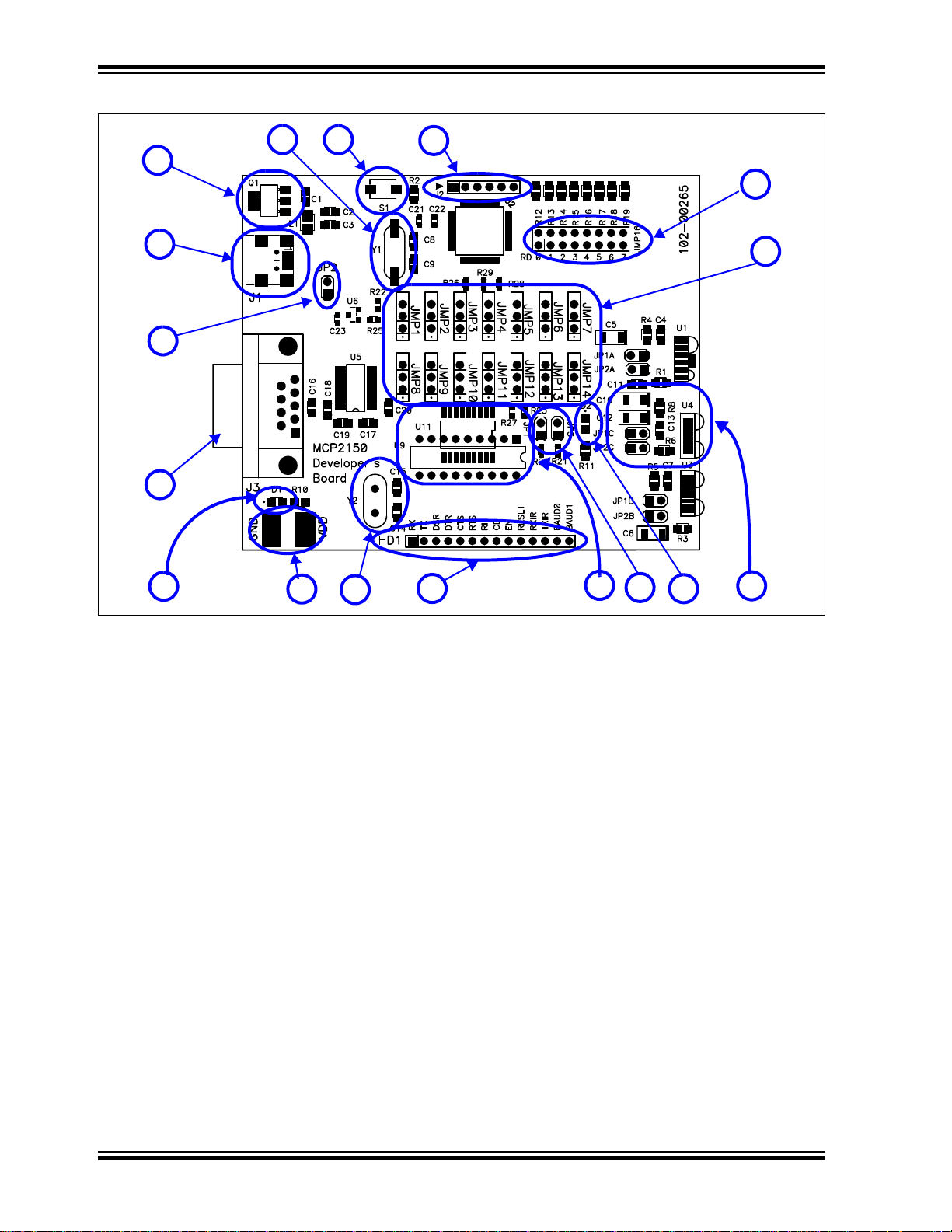
The MCP2150 Developer’s Board, as shown in Figure 1-1, has the following hardware
features:
1. Mini USB connector (for powering the board).
2. On Board +3.3V regulator for powering PIC18F65J50.
3. Hooks for an external regulated DC supply.
4. Jumper to Isolate PIC18F65J50 power signal from rest of board power. This
allows the board to operate at voltages higher than 3.3V.
5. DB-9 connector and associated hardware for direct connection to MCP2150
UART (DB-9 interface requires RS-232 signal levels).
6. Fourteen-pin header connection to Host UART interface.
7. Fourteen 1x3 pin jumpers for routing of the UART signals between the
MCP2150, PIC18F65J50, and MAX3238 devices.
8. MCP2150 BAUD1:BAUD0 state jumpers.
9. Green power-on indicator LED.
10. Implemented IR transceiver circuit (two optional optical transceiver circuits
implemented but not populated).
11. Reset switch for PIC18F65J50 device.
12. ICSP Header for PIC18F65J50.
13. Jumper option for PIC18F65J50 program selection.
14. PIC18F65J50 crystal.
15. MCP2150 crystal socket.
16. Carrier Detect (CD) indicator LED.
17. MCP2150 SOIC and DIP Footprints (SOIC package is default installation. To
install the DIP package requires the removal of the SOIC package).
Note: A schematic of the MCP2150 Developer’s Board is shown in
Section A.2 “Board - Schematic - Page 1”
© 2009 Microchip Technology Inc. DS51869A-page 13
Page 14
MCP2150 Developer’s Board User’s Guide
BOARD EDGE
2
3
5
6
9
4
11
12
8
13
7
10
15
17
14
1
16
FIGURE 1-1: MCP2150 DEVELOPER’S BOARD HARDWARE
DS51869A-page 14 © 2009 Microchip Technology Inc.
Page 15
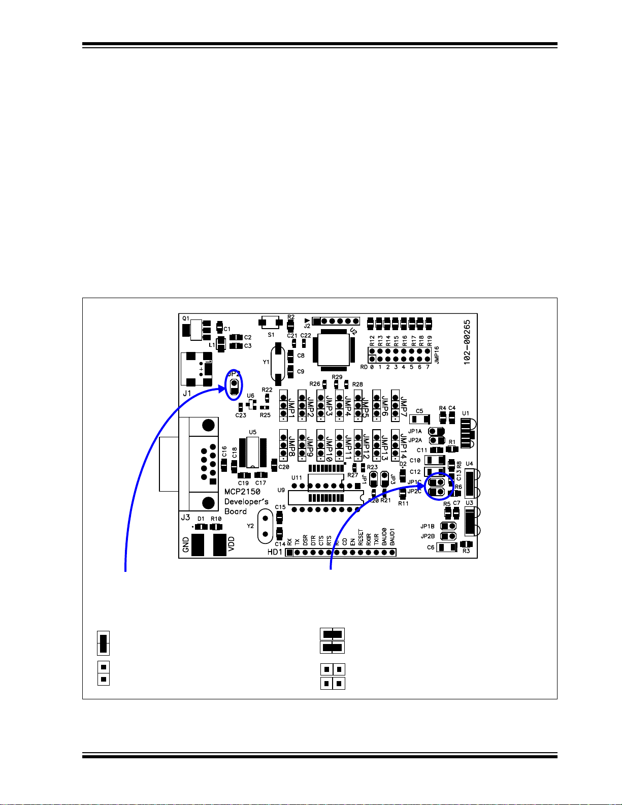
1.3.1 Selecting Power Source, and Optical Transceiver Interface
BOARD EDGE
VDD’s planes are isolated
V
DD’s planes are connected
This jumper isolates the PIC19’s VDD
from the MCP2150 V
DD plane (see
Section A.8 “Board - Power Layer”)
JP2
These two jumpers select the optical transceiver logic.
Both jumpers should connect the same pin positions.
JP1x1 and JP2x1
Optical Transceiver connected to
MCP2150 IR Interface
Optical Transceiver not connected
to MCP2150 IR Interface
Jumper Descriptions
Figure 1-2 shows the jumpers used to control the power source, and the optical
transceiver used.
Jumper JP2 connects to the boards two power planes. The MCP2150 Developer’s
Board has a power plane for the PIC18F65J5 0 and the re lated circuitry, and a second
power plane for all other circuitry . Removing the jumper allows the MCP2150 portion to
operate through the full voltage range of the MCP2150 (2.0V to 5.5V). When JP2 is
connected, then the maximum voltage is restricted to the ma xim u m vo ltage of the
PIC18F65J50 device (3.6V). See Figure A.8 for the power plane layout. When JP2 is
open, then the PIC18F65J50 must be isolated from the MCP2150. Th is is done with
the JMP1:JMP14 jumpers as well as the R26, R27, R28, and R29 resisto rs.
Jumpers JP1C1 and JP2C1 are used to connect the default installed optical transceiver
to the MCP2150’s RXPD and TXIR pins. There are footprints for two other optical
transceiver implementations. If either of those implementations are installed, then the
jumpers may be switched to the desired optical transceiver.
FIGURE 1-2: MCP2150 SELECTING SOURCES
Product Overview
© 2009 Microchip Technology Inc. DS51869A-page 15
Page 16
MCP2150 Developer’s Board User’s Guide
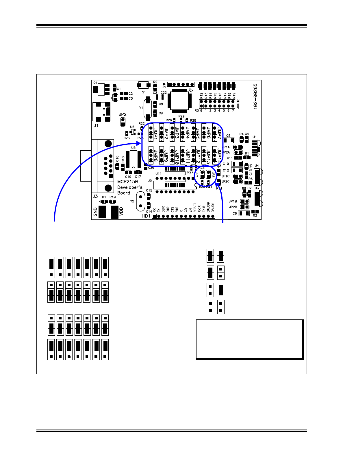
BOARD EDGE
Host UART Signals connected
These fourteen jumpers connect the MCP2150’s Host UART
Signals to either the PIC18F65J50 or the DB-9 connector
(after the UART Driver device)
JMP1:JMP7 / JMP8:JMP14
Host UART Signals connected
to PIC18F65J50
to UART Driver (DB-9)
MCP2150 Host Interface
Baud Rate select Signals
JP3:JP1
Host Interface operates at
Host Interface operates at
Host Interface operates at
Host Interface operates at
1 15,200 Baud
57,600 Baud
19,200 Baud
9,600 Baud
Note: T h e PIC ca n also driv e th es e
signals. The supplied firmware
uses PIC I/O to drive these
signals based on the state of
the RD5:4 pins.
1.3.2 Host UART Interface Connection Jumper Descriptions
Figure 1-3 shows the five jumpers used to control the connection of the MCP2150’s
Host UART signals.
FIGURE 1-3: MCP2150 HOST UART INTERFACE CONNECTION
DS51869A-page 16 © 2009 Microchip Technology Inc.
Page 17

Product Overview
1.4 PC REQUIREMENTS
The PC used has three main requirements. These are:
1. Standard serial port.
2. USB port (to power the MCP2150 Developer’s Board).
3. Terminal emulation program.
4. IrDA standard driver installed, which treats the IR port as a vir tual serial port.
A non-legacy-free Intel
would meet these requirements. The Windows
program called Hyperterminal. Section Appendix D. “Configuring the
HyperTerminal
®
demonstrate the developer’s boards.
1.5 WHAT THE MCP2150 DEVELOPER’S BOARD KIT INCLUDES
This MCP2150 Developer’s Board kit includes:
• MCP2150 Developer’s Board, 102-00265
• Important Information Sheet
®
compatible model with Windows Operating System (OS)
®
OS includes a terminal emulation
Program” shows instructions to configure HyperTerminal and
NOTICE
The Kits no longer ship with CD-ROMs. Any other material is available for download from
the Developments Boards product page. This material can include such items as:
• User’s Guide
•Firmware
• GUI programs
• Schematic Capture and PCB Layout files
© 2009 Microchip Technology Inc. DS51869A-page 17
Page 18

MCP2150 Developer’s Board User’s Guide
NOTES:
DS51869A-page 18 © 2009 Microchip Technology Inc.
Page 19

Chapter 2. Installation and Operation
2.1 INTRODUCTION
T o d emonstrate the operation of the MCP2150 Develope r’s Board (Secondary Device)
a Primary Device is required. The Primary Device can be a PC with an IR port
(integrated IR port or IR Dongle).
The MCP2150 Developer’s Board default firmware program has four different
programs that are selected by the state of the RD7:6 pins .
These demonstration programs have the following operation:
• Demo #1 Operation - Direct IR / UART (DB-9) Mode
• Demo #2 Operation - Data Streaming Mode
• Demo #3 Operation - Echo Data Mode
• Demo #4 Operation - IR / UART (DB-9) Pass Through PIC Mode
Each demonstration program’s operation will be described in the Demo section.
The component layout floor plan of the MCP2150 Developer’s Board (MCP2150DM)
PCB is shown in Figure 1-1 while Table 2-1 shows the hardware requirements to
demonstrate the MCP2150 Developer’s Board.
MCP2150 DEVELOPER’S BOARD
USER ’S GUIDE
TABLE 2-1: DEMO SYSTEM HARDWARE REQUIREMENTS
Qty Hardware Purpose
1 PC with: (1)
a) IR port
or
PC with USB/Serial port and
USB/Serial port to IR Dongle
(1)
b) One USB port to power the
MCP2150 Developer’s
Board
and
c) one serial port to
communicate to the
MCP2150 Developer’s
Board.
1 Serial Cable To connect the PC serial ports to the MCP2150 Developer’s
1 USB Cable To power the MCP2150 Developer’s Board from the PC’s USB
— MCP2150 Developer’s Board This is the demonstration unit
Note 1: This can be done with one PC, but depending on the features of the selected PC, a second PC
may be required due to number of serial ports available (see Figure 2-1).
T o keep the board cost low , only a por tion of the MCP2150 Developer’s Board is tested.
This test covers the major portions of the system. The portions th at ar e not tested a re
shown in Appendix C. “Board Testing”.
As a Primary Device, this device will initiate communication to
the MCP2150 Developer’s Board. The PC’s USB port will also
power the MCP2150 Developer’s Board.
Also:
The PC’s UART port will “talk” with the MCP2150’s UART
interface, while the PC’s IR port will “talk” with the MCP2150’s
IR interface.
The PC will run two instances of HyperTerminal, one
connected to the PC’s serial port (UART) and the other
connected to the PC’s IR port.
Board serial port.
port.
© 2009 Microchip Technology Inc. DS51869A-page 19
Page 20

MCP2150 Developer’s Board User’s Guide
2.2 THE DEMO SYSTEM
The demo system setup requires a Primary Device and a MCP2150 Developer’s Board
(Secondary Device). The Primary Device is a PC with an IR port (integrated IR port or
IR Dongle). The Secondary Device is the embedded system, which is the MCP2150
Developer’s Board.
The MCP2150 Developer’s Board can be powered by one of two sources:
• The USB sourced power
• The Power supply test points
For the demo descriptions, the board will be powered via USB, so, a PC with a UART
and USB port is required. The USB voltage is regulated to 3.3V, due to the PIC18
device’s voltage operating range.
This developer board either communicates between the DB-9 interface and the IR
interface or acts as an embedded syste m and communicates between the IR interface
and the PIC microcontroller.
2.2.1 The PIC18F65J50 Firmware
The PIC18F65J50 firmware program looks at the state of the RD7:4 pins to determine
the board’s operation (program an d Host UART baud rate).
The configuration of the JMP14:JMP1 jumpers determines how th e UART signals are
connected between the MCP2150, PIC and the MAX3238 compatible driver.
The programs have the following operations:
• Data is directly passed from the IR interface to the MAX3238 device
• Data is passed from the IR interface to the MAX3238 device af ter pa ssing through
the PIC microcontroller
• Once a data byte has been received by the PIC, the PIC continuously stream s a
data table
• The PIC echoes whatever character it receives, after changing the case (upper to
lower, and lower to upper)
2.2.2 The PC with IR Port
A PC with IR Port can be configured to operate as the Primary Device. The PC will need
to run an appropriate application program to communicate with the Second ary Device.
For a PC with IR port, this program will be HyperTerminal. The IRCOMM2K driver may
need to be installed so that HyperTerminal can communicate to the IR port as if it was
a serial port. When installing IRCOMM2K, select COM7 as the desired port.
Configuring the HyperTerminal program on the PC is shown in D.1.2 “Configuring
HyperTerminal to connect to the IrDA Port (Virtual Port)”.
The PC will run a second instance of HyperT erminal when running Demo #1 and Demo
#4. This instance of HyperTerminal will communicate to the PC’s serial port which will
be connected to the MCP2150DM’s serial port. This allows the transmitted data (from
the IR port) to be seen on the serial port (and vice versa). Configuring the
HyperTerminal program on the PC is shown in D.1.3 “HyperTerminal Configuration
for the Secondary Device”.
Note: HyperTerminal should be disabled before establishing a connection
between the PC and the MCP2150 Developer’s Board. Make sure that any
other programs (e.g., HotSync
®
) connected to the IR ports are disabled.
DS51869A-page 20 © 2009 Microchip Technology Inc.
Page 21

2.3 MCP2150DM DEMOS
HyperTerminal
¬
Program Window A
(to IrDA Dongle)
(1)
(Com 1)
(2)
Com 1
System #1
(1)
System #2
MCP2150 Developer’s
Board
Serial (UART or USB)
to IrDA Dongle
HyperTerminal
Program Window B
(2)
(3)
Note 1: The PC may be a Notebook with an Integrated IR port. This operates as the Primary
Device.
2: Serial cable. Connects Secondary Device to PC.
3: USB cable (for power only).
Monitor
PC
A description of the demos, including step-by-step instructions are shown in this
section.
2.3.1 Demo #1 Operation - Direct IR / UART (DB-9) Mode
In Demo #1, the MCP2150 Developer’s Board will communicate directly to the PC
(or IrDA to serial interface Dongle) data received on the DB-9 port.
This demo shows the MCP2150 converting data between the IR port and the Host
UART port. The Primary Device’s IR p acket is decode d and any data is extracted and
Transmitted on the Host UART interface. Data received on the Host UART interface is
formatted into the IR data packet and transmitted to the Primary device.
Figure 2-1 shows the system setup, while Figure 2-2 shows the jumper configuration
for the MCP2150 board. Lastly, Table 2-2 shows the steps for Demo #1 operation.
Note: Figure 2-3 shows an alternate jumper configuration where the
MCP2150DM is powered via the V
JP2 shunt be removed). Table 2.3.2 does not document this configuration,
but due to its similarities should be easy for the user to implement.
Installation and Operation
DD and GND test points (requires that
FIGURE 2-1: DEMO #1 SYSTEM BLOCK DIAGRAM
(1)
Hyperterminal to Serial Port Settings
The com port settings should be configured as:
• 115,200 Baud
•8-bits
•No Parity
• One Stop
• Hardware Flow Control
© 2009 Microchip Technology Inc. DS51869A-page 21
Page 22

MCP2150 Developer’s Board User’s Guide
BOARD EDGE
Data Flow
IR
Transceivers
DB-9
Connector
FIGURE 2-2: DEMO #1 CONFIGURATION - DIRECT TO UART (DB-9) MODE
Note: This is the board configuration shipped to customers.
DS51869A-page 22 © 2009 Microchip Technology Inc.
Page 23

Installation and Operation
BOARD EDGE
Data Flow
IR
Transceivers
DB-9
Connector
VDDGND
Jumper Shunt
Removed
FIGURE 2-3: DEMO #1 ALTERNATE POWER CONFIGURATION
© 2009 Microchip Technology Inc. DS51869A-page 23
Page 24

MCP2150 Developer’s Board User’s Guide
TABLE 2-2: DEMO #1 STEPS
Step Action Result
1 Place the Primary Device’s IR port and the MCP2150
Developer’s Board on a flat surface about 25 cm (10
inches) apart, and with the IR ports facing each other.
2 On the MCP2150 Developer’s Board:
Ensure that the jumpers are configured as in
Figure 2-2.
3 On the MCP2150 Developer’s Board:
Apply power to the unit via the USB connector. The PIC
reset switch (S1) may be depressed and released to
ensure that the PIC had a good reset.
4 Connect PC’s Serial Port to the DB-9 connector of the
MCP2150 Developer’s Board.
5 On the PC:
Wait for the PC to make a sound and the system tray
shows an IR Icon. Placing the mouse over the Icon will
show the MCP2150 Device ID (currently “Generic
IrDA”).
6 On the PC:
Open the HyperTerminal program window for the
Primary Device (such as COM 7).
Ensure that the window indicates that the HyperT erminal
program is connected.
Note: See D.1.2 “Configuring HyperTerminal to
connect to the IrDA Port (Virtual Port)”
7 On the PC:
Open a second instance of HyperTerminal program
window attached to the PC’s Serial Port (such as
COM 2) to connect to the MCP2150 Developer’s Board.
Ensure that the window indicates that the HyperT erminal
program is connected.
Note: See D.1.3 “HyperT e rmi na l Co nfi gu ra ti on
for the Secondary Device”
8 On the PC:
In one of the HyperTerminal program windows (such as
the Primary Device’s window), type some characters.
9 On the PC:
In the other HyperTerminal program windows (Serial
Port window), type some characters.
10 On the PC:
In either HyperTerminal pr ogram windows, select the
Transfer pull-down menu and then the Send Text File ...
option. Navigate to the folder that contains the
Transmit File.Txt file and select it. Then, click
Open.
11 On the PC:
Make this file transfer transmitting from the other
HyperTerminal prog ram window.
12 Continue steps 8, 9 10, or 11 for as long as desired. —
—
—
On the MCP2150 Developer’s Board:
The green power LED (D1) will turn on.
—
—
On the MCP2150 Developer’s Board:
—
On the PC:
The system tray Icon will change from a single IR
Icon to two IR Icons facing each other. An IR Link is
now established.
—
On the PC:
In the other HyperTerminal program windows (the
Serial Port window), those characters appear.
On the PC:
In the other HyperTerminal program windows (the
Primary Device’s window), those characters
appear.
On the PC:
In the selected HyperTerminal program window, the
displayed data is transmitted, being received and
displayed by the other HyperTerminal program
window.
On the PC:
In the selected HyperTerminal program window, the
displayed data is transmitted, being received and
displayed by the other HyperTerminal program
window.
DS51869A-page 24 © 2009 Microchip Technology Inc.
Page 25

Installation and Operation
HyperTerminal
¬
Program Window A
(to IrDA Dongle)
(1)
System #1
(1)
System #2
MCP2150 Developer’s
Board
Serial (UART or USB)
to IrDA Dongle
(2)
Note 1: The PC may be a Notebook with an Integrated IR port. This operates as the Primary
Device.
2: USB cable (for power only).
Monitor
PC
2.3.2 Demo #2 Operation - Data Streaming Mode
In Demo #2, the MCP2150 Developer’s Board (MCP2150DM) will communicate via the
IR interface to the PC. The MCP2150DM is the Secondary Device, and will
continuously stream a data table to the Primary Device (PC). This shows the data
throughput from the embedded system to the Primary Device. This throu ghput will vary
depending on the characteristics of the Primary Device.
Figure 2-4 shows the system setup for this test, while Figure 2-5 shows the jumper
configuration for the MCP2150 board. Lastly, Table 2-3 shows the steps for Demo #2
operation.
Note: Figure 2-6 shows an alternate jumper configuration where the
MCP2150DM is powered via the V
JP2 shunt be removed). Table 2-6 does not document this configuration
but, due to its similarities, should be easy for the user to implement.
DD and GND test points (requires that
FIGURE 2-4: DEMO #2 SYSTEM BLOCK DIAGRAM
(1)
© 2009 Microchip Technology Inc. DS51869A-page 25
Page 26

MCP2150 Developer’s Board User’s Guide
BOARD EDGE
D
a
t
a
F
l
o
w
IR
Transceivers
PIC18F65J50
FIGURE 2-5: DEMO #2 CONFIGURATION - DATA STREAMING MODE
DS51869A-page 26 © 2009 Microchip Technology Inc.
Page 27

Installation and Operation
BOARD EDGE
D
a
t
a
F
l
o
w
IR
Transceivers
PIC18F65J50
VDDGND
Jumper Shunts
Removed
FIGURE 2-6: DEMO #2 ALTERNATE POWER CONFIGURATION
© 2009 Microchip Technology Inc. DS51869A-page 27
Page 28

MCP2150 Developer’s Board User’s Guide
TABLE 2-3: DEMO #2 STEPS - DATA STREAMING MODE
Step Action Result
1 Place the Primary Device’s IR port and the MCP2150
Developer’s Board on a flat surface about 25 cm (10
inches) apart, and with the IR ports facing each other.
1 On the MCP2150 Developer’s Board:
Ensure that the jumpers are configured as in
Figure 2-5.
2 On the MCP2150 Developer’s Board:
Apply power to the unit via the USB connector. The
PIC reset switch (S1) may be depressed and
released to ensure that the PIC had a good reset.
3 On the PC:
Open the HyperTerminal program window for the
Primary Device (such as COM 7).
Ensure that the window indicates that the
HyperTerminal prog ram is connected.
Note: See D.1.2 “Configuring HyperTerminal
to connect to the IrDA Port (Virtual
Port)”
4 On the PC:
In the HyperTerminal program window, type any
character.
5 On the PC:
Disconnect the HyperTerminal program window.
—
—
On the MCP2150 Developer’s Board:
The green power LED (D1) will turn on.
On the MCP2150 Developer’s Board:
—
On the PC:
The system tray Icon will change from a single IR
Icon to two IR Icons facing each other. An IR Link is
now established.
On the MCP2150 Developer’s Board:
—
On the PC:
Then, a continuous stream of a 250 Byte table will be
received from the embedded system in the
HyperTerminal window (See for Appendix
E. “Continuously Transmitted Data Table”)
On the PC:
HyperTermina l program window no longer receives
data.
DS51869A-page 28 © 2009 Microchip Technology Inc.
Page 29

Installation and Operation
HyperTerminal
¬
Program Window A
(to IrDA Dongle)
(1)
System #1
(1)
System #2
MCP2150 Developer’s
Board
Serial (UART or USB)
to IrDA Dongle
(2)
Note 1: The PC may be a Notebook with an Integrated IR port. This operates as the Primary
Device.
2: USB cable (for power only).
Monitor
PC
2.3.3 Demo #3 Operation - Echo Data Mode
In Demo #3, the MCP2150 Developer’s Board (MCP2150DM) will communicate via the
IR interface to the PC. The MCP2150DM is the Secondary Device, and will echo the
received data (after changing the case) to the Primary Device (PC). This shows the
command/response of an application system.
Figure 2-7 shows the system setup for this test, while Figure 2-8 shows the jumper
configuration for the MCP2150 board. Lastly, Table 2-4 shows the steps for Demo #2
operation.
FIGURE 2-7: DEMO #3 SYSTEM BLOCK DIAGRAM
(1)
© 2009 Microchip Technology Inc. DS51869A-page 29
Page 30

MCP2150 Developer’s Board User’s Guide
BOARD EDGE
D
a
t
a
F
l
o
w
IR
Transceivers
PIC18F65J50
FIGURE 2-8: DEMO #3 CONFIGURATION - ECHO DATA MODE
DS51869A-page 30 © 2009 Microchip Technology Inc.
Page 31

Installation and Operation
TABLE 2-4: DEMO #3 STEPS - ECHO DATA MODE
Step Action Result
1 Place the Primary Device’s IR port and the MCP2150
Developer’s Board on a flat surface about 25 cm (10
inches) apart, and with the IR ports facing each other.
2 On the MCP2150 Developer’s Board #1:
Ensure that the jumpers are configured as in
Figure 2-5. Jumpers shown in green are not required
and can be left open.
3 On the MCP2150 Developer’s Boards:
Apply power to the unit via the USB connector.
4 On the PC:
Open the HyperTerminal program window for the
Primary Device (such as COM 7).
Ensure that the window indicates that the HyperT erminal
program is connected.
Note: See D.1.2 “Configuring HyperTerminal to
connect to the IrDA Port (Virtual Port)”
5 On the PC:
In the HyperTerminal program window, type some alpha
characters, such as “kLwtGh”.
6 Continue typing any alpha characters (upper or lower
case)
7 On the PC:
Disconnect the HyperTerminal program window.
—
—
On the MCP2150 Developer’s Board:
The green power LED (D1) will turn on.
On the MCP2150 Developer’s Board:
—
On the PC:
The system tray Icon will change from a single IR
Icon to two IR Icons facing each other. An IR Link is
now established.
On the PC:
The HyperTerminal program window will display
each character and its switched case version. So,
“kLwtGh” will show “kKLlwWtTGghH”.
The alpha character typed and its opposite case will
be displayed (such as “aA”, “Aa”, “Bb”, ...)
On the PC:
HyperTer minal program window no longer receives
data.
© 2009 Microchip Technology Inc. DS51869A-page 31
Page 32

MCP2150 Developer’s Board User’s Guide
HyperTerminal
¬
Program Window A
(to IrDA Dongle)
(1)
(Com 1)
(2)
Com 1
System #1
(1)
System #2
MCP2150 Developer’s
Board
Serial (UART or USB)
to IrDA Dongle
HyperTerminal
Program Window B
(2)
(3)
Note 1: The PC may be a Notebook with an Integrated IR port. This operates as the Primary
Device.
2: Serial cable. Connects Secondary Device to PC.
3: USB cable (for power only).
Monitor
PC
2.3.4 Demo #4 Operation - IR / UART (DB-9) Pass Through PIC Mode
In Demo #4, the MCP2150 Developer’s Board will communicate to the PC (or IrDA to
serial interface Dongle) data received on the DB-9 port.
This demo shows the MCP2150 converting data between the IR port and the Host
UART port. The Primary Device’s IR packet is decode d and an y dat a is extracted an d
transmitted on the Host UART interface. Data received on the Host UART interface is
formatted into the IR data packet and transmitted to the Primary device.
Figure 2-9 shows the system setup for this test, while Figure 2-10 shows the jumper
configuration for the MCP2150 board. Lastly, Table 2-5 shows the steps for Demo #4
operation.
FIGURE 2-9: DEMO #4 SYSTEM BLOCK DIAGRAM
Hyperterminal to Serial Port Settings
The com port settings should be configured as:
• 115,200 Baud
•8-bits
•No Parity
• One Stop
• Hardware Flow Control
(1)
DS51869A-page 32 © 2009 Microchip Technology Inc.
Page 33

Installation and Operation
BOARD EDGE
D
a
t
a
F
l
o
w
IR
Transceivers
PIC18F65J50
D
a
t
a
F
l
o
w
DB-9
Connector
RX2
TX1
RX1
TX2
FIGURE 2-10: DEMO #4 CONFIGURATION - PASS THROUGH PIC MODE
© 2009 Microchip Technology Inc. DS51869A-page 33
Page 34

MCP2150 Developer’s Board User’s Guide
TABLE 2-5: DEMO #4 STEPS - PASS THROUGH PIC MODE
Step Action Result
1 Place the Primary Device’s IR port and the MCP2150
Developer’s Board on a flat surface about 25 cm (10
inches) apart, and with the IR ports facing each other.
2 On the MCP2150 Developer’s Board:
Ensure that the jumpers are configured as in
Figure 2-10.
3 On the MCP2150 Developer’s Board:
Apply power to the unit via the USB connector. The PIC
reset switch (S1) may be depressed and released to
ensure that the PIC had a good reset.
4 Connect PC’s Serial Port to the DB-9 connector of the
MCP2150 Developer’s Board.
5 On the PC:
Wait for the PC to make a sound and the system tray to
show an IR Icon. Placing the mouse over the Icon will
show the MCP2150 Device ID (currently “Generic
IrDA”).
6 On the PC:
Open the HyperTerminal program window for the
Primary Device (such as COM 7).
Ensure that the window indicates that the HyperT erminal
program is connected.
Note: See D.1.2 “Configuring HyperTerminal to
connect to the IrDA Port (Virtual Port)”
7 On the PC:
Open a second instance of HyperTerminal program
window attached to the PC’s Serial Port (such as
COM 2) to connect to the MCP2150 Developer’s Board.
Ensure that the window indicates that the HyperT erminal
program is connected.
Note: See D.1.3 “HyperT e rmi na l Co nfi gu ra ti on
for the Secondary Device”
8 On the PC:
In one of the HyperTerminal program windows (such as
the Primary Device’s window), type some characters.
9 On the PC:
In the other HyperTerminal program windows (Serial
Port window), type some characters.
10 On the PC:
In either HyperTerminal pr ogram windows, select the
Transfer pull-down menu and then the Send Text File ...
option. Navigate to the folder that contains the
Transmit File.Txt file and select it. Then click
Open.
11 On the PC:
Make this file transfer transmitting from the other
HyperTerminal prog ram window.
12 Continue steps 8, 9 10, or 11 for as long as desired. —
—
—
On the MCP2150 Developer’s Board:
The green power LED (D1) will turn on.
—
—
On the MCP2150 Developer’s Board:
—
On the PC:
The system tray Icon will change from a single IR
Icon to two IR Icons facing each other. An IR Link is
now established.
—
On the PC:
In the other HyperTerminal program windows (the
Serial Port window), those characters appear.
On the PC:
In the other HyperTerminal program windows (the
Primary Device’s window), those characters
appear.
On the PC:
In the selected HyperTe rmin al program window the
displayed data is transmitted and is received and
displayed by the other HyperTerminal program
window.
On the PC:
In the selected HyperTerminal program window, the
displayed data is transmitted, being received and
displayed by the other HyperTerminal program
window.
DS51869A-page 34 © 2009 Microchip Technology Inc.
Page 35

MCP2150 DEVELOPER’S BOARD
Top Layer
Ground Layer
Power Layer
Bottom Layer
USER ’S GUIDE
Appendix A. Schematic and Layouts
NOTICE TO CUSTOMERS
All documentation becomes dated, and this manual is no exception. Microchip tools and
documentation are constantly evolving to meet customer needs, so some schematics and
board layouts may differ from those in this document. Please refer to our web site
(www.microchip.com) to obtain the latest documentation available.
A.1 INTRODUCTION
This appendix contains the following schematics and layouts for the MCP2150
Developer’s Board:
• Board - Schematic
• Board - Top Silk and Pads
• Board - Top Layer
• Board - Top Silk and Pads Top layer
• Board - Bottom Layer
•Board - V
• Board - Ground Layer
The layer order is shown in Figure A-1.
DD Layer
FIGURE A-1: LAYER ORDER
© 2009 Microchip Technology Inc. DS51869A-page 35
Page 36

MCP2150 Developer’s Board User’s Guide
M
12
CTS
9
RI
1
BAUD0
2
TXIR
15
OSC2
17CD11
DTR
8
RX5VSS
13
RTS
7
TX
10
DSR
6
EN
14
VDD
18
BAUD1
3
RXIR
4
R
ESET
16
OSC1/CLKI
12
CTS
9
RI
1
BAUD0
2
TXIR
15
OSC2
17CD11
DTR
8
RX5VSS
13
RTS
7
TX
10
DSR
6
EN
14
VDD
18
BAUD1
3
RXIR
4
R
ESET
16
OSC1/CLKI
A.2 BOARD - SCHEMATIC - PAGE 1
DS51869A-page 36 © 2009 Microchip Technology Inc.
Page 37

A.3 BOARD - SCHEMATIC - PAGE 2
M
Schematic and Layouts
© 2009 Microchip Technology Inc. DS51869A-page 37
Page 38

MCP2150 Developer’s Board User’s Guide
BOARD EDGE
A.4 BOARD - TOP SILK AND PADS
DS51869A-page 38 © 2009 Microchip Technology Inc.
Page 39

A.5 BOARD - TOP LAYER
Schematic and Layouts
© 2009 Microchip Technology Inc. DS51869A-page 39
Page 40

MCP2150 Developer’s Board User’s Guide
BOARD EDGE
A.6 BOARD - TOP LAYER WITH SILK AND PADS
DS51869A-page 40 © 2009 Microchip Technology Inc.
Page 41

A.7 BOARD - BOTTOM LAYER
Schematic and Layouts
© 2009 Microchip Technology Inc. DS51869A-page 41
Page 42

MCP2150 Developer’s Board User’s Guide
A.8 BOARD - POWER LAYER
DS51869A-page 42 © 2009 Microchip Technology Inc.
Page 43

A.9 BOARD - GROUND LAYER
Schematic and Layouts
© 2009 Microchip Technology Inc. DS51869A-page 43
Page 44

MCP2150 Developer’s Board User’s Guide
NOTES:
DS51869A-page 44 © 2009 Microchip Technology Inc.
Page 45

MCP2150 DEVELOPER’S BOARD
USER ’S GUIDE
Appendix B. Bill Of Materials (BOM)
NOTICE TO CUSTOMERS
All documentation becomes dated, and this manual is no exception. Microchip tools and
documentation are constantly evolving to meet customer needs, so the Bill Of Materials may
differ from those in this document. Please refer to our web site (www.microchip.com) to
obtain the latest documentation available.
The MCP2150 Developer’s Board allows the MCP2150 device to be evaluated. The
board supports customers in the evaluation of three additional optical transceiver
devices. This is done with component layout of these additional optical transceiver
circuits. The customer would be required to install the desired circui t for testing.
T able B-1 shows the components that are installed in the MCP2150 Developer’s Board
PCB, while Table B-2 shows the components that are NOT installed on the MCP2150
Developer’s Board PCB.
TABLE B-1: BILL OF MATERIALS (BOM)
Qty Reference Description Manufacturer Part Number
2 C1,C2 CAP 1.0UF 16V CERAMIC X7R 0805 Kemet C0805C105K4RACTU
9 C3, C7, C11,
C13, C16, C17,
C18, C19, C20
2 C21, C23 CAP .1UF 25V CERAMIC X7R 0603 Panasonic - ECG ECJ-1VB1E104K
4 C8, C9 CAP CERAMIC 22PF 50V NP0 0805 Kemet
2 C10, C12 CAPACITOR 4.7UF/10V TEH SER SMD Panasonic - ECG ECS-H1AX475R
1 C22 CAP 4.7UF 10V X53 0603 Panasonic - ECG C0603C475K8PACTU
2 D1, D2 LED GREEN CLEAR 0805 SMD LITE-ON
1 HD1 CONN HEADER.100 SINGL STR 12POS Sullins Connector
1 J1 CONN RECEPT MINI USB2.0 5POS Hirose Electronic Co.
1 J2 CONN HEADER.100 SINGL STR 6POS
1 J3 CONN D-SUB RCPT R/A 9POS PCB AU Amphenol
CAP .1UF 25V CERAMIC X7R 0805 Panasonic
Corp.
Semiconductor Corp.
Solutions
Ltd
Sullins Connector
(Note 2)
Solutions
Commercial Products
®
- ECG ECJ-2VB1E104K
®
Electronics
®
C0805C220J5GACTU
LTST-C170CKT
PEC12SAAN
UX60-MB-5ST
PEC06SAAN
6E17C-009S-AJ-120
Note 1: The components listed in this Bill of Materials are representative of the PCB assembly. The
released BOM used in manufacturing uses all RoHS-compliant components.
2: This connector can be made by cutting a single .100 Single R/A 36POS into six pieces.
© 2009 Microchip Technology Inc. DS51869A-page 45
Page 46

MCP2150 Developer’s Board User’s Guide
TABLE B-1: BILL OF MATERIALS (BOM) (CONTINUED)
Qty Reference Description Manufacturer Part Number
14 JMP1, JMP2,
CONN HEADER 3POS .100" STR TIN Molex
JMP3, JMP4,
JMP5, JMP6,
JMP7, JMP8,
JMP9, JMP10,
JMP11, JMP12,
JMP13, JMP14
1 JMP6 CONN HEADER 16POS .100 VERT
GOLD
5 JP1, JP2, JP3
CONN HEADER 2POS .100 VERT TIN Molex/Waldom
JP1C, JP2C
1 L1 INDUCTOR POWER 10UH 1008 TDK
1 PCB RoHS Compliant Bare PCB, MCP2150
Developer’s Board
1 Q1 300mA CMOS LDO Microchip Technology
9 R2, R12, R13,
RES 10K OHM 1/8W 5% 0805 SMD Panasonic - ECG ERJ-6GEYJ103V
R14, R15, R16,
R17, R18, R19
4 R20, R21, R22,
RES 10K OHM 1/10W 5% 0603 SMD Panasonic - ECG ERJ-3GEYJ103V
R23
1 R6 RES 0.0 OHM 1/8W 5% 0805 SMD Panasonic - ECG ERJ-6GEY0R00V
1 R8 RES 47 OHM 1/8W 5% 0805 SMD Panasonic - ECG ERJ-6GEYJ470V
2 R10, R11 RES 470 OHM 1/8W 5% 0805 SMD Panasonic - ECG ERJ-6GEYJ471V
1 R25 RES 100 OHM 1/10W 5% 0603 SMD Panasonic - ECG ERJ-3GEYJ101V
4R26, R27,
RES 10K OHM 1/10W 5% 0603 SMD Panasonic - ECG ERJ-3GEYJ102V
R28,R29
1 S1 SWITCH LT TOUCH 6X3.5 100GF SMD Panasonic - ECG EVQ-PE104K
1 U2 64/80-Pin High-Performance, 1-Mbit Flash
USB Microcontrollers
1 U5 Intelligent +3.0V to +5.5V RS-232
Transceiver
1 U6 MCP111 Micropower Voltage Detector Microchip Technology
1 U11 MCP2150 SOIC-18 IrDA
®
Standard
Protocol Stack Controller
1 U4 Infrared Transceivers SIR 115.2 kbits/s Vishay
2V
DD, GND TEST POINT PC COMPACT SMT Keystone
1 Y1 CRYSTAL 14.7456 MHZ 20PF SMD CTS-Frequency Controls ECS-147.4-20-5P-TR
2 Y2 PIN RECPT .015/.025 DIA 0667 SER Mill-Max Manufacturing 0667-0-15-01-30-27-10-0
4 Bottom side on
Each Corner
17 Shunts for JP2,
JP1C, JP2C,
JMP1-JMP14
BUMPON HEMISPHERE .44X.20 BLACK 3M SJ-5003 (BLACK)
.100" Shorting Block with Handle JAMECO
Note 1: The components listed in this Bill of Materials are representative of the PCB assembly. The
released BOM used in manufacturing uses all RoHS-compliant components.
2: This connector can be made by cutting a single .100 Single R/A 36POS into six pieces.
®
/Waldom®
90120-0123
Electronics Corp
Molex/Waldom
10-89-1161
Electronics Corp.
22-03-2021
Electronics Corp
®
Corporation NLV25T-100J-PF
Microchip T echnology
104-00265
Inc.
TC1108-3.3VDB
Inc.
Microchip T echnology
PIC18F86J50-I/PT
Inc.
SIPEX SP3238EEY-L
MCP11 1-315E/TT
Inc.
Microchip T echnology
MCP2150T-I/SO
Inc.
®
TFDU4300-TR3
Semiconductor
®
5016
Electronics
®
VALUEPRO 2012JH-R
DS51869A-page 46 © 2009 Microchip Technology Inc.
Page 47

Bill Of Materials (BOM)
TABLE B-2: TABLE OF CONTENTS (BOM) – PCB COMPONENTS NOT INSTALLED
Qty Reference Description Manufacturer Part Number
0 C4 CAP .47UF 16V CERAMIC X7R 080 Panasonic - ECG ECJ-2YB1C474K
0 C5 AP TANTALUM 6.8UF 16V 20% SMD Nichicon
Corporation
0 C6 CAP 4.7UF 16V CERAMIC F 0805 Panasonic - ECG ECJ-2FF1C475Z
0 C7 CAP .1UF 25V CERAMIC X7R 0805 Panasonic - ECG ECJ-2VB1C104K
0 JP1A, JP1B,
JP2A, JP2B
0 R1 RES 2.2 OHM 1/8W 1% 0805 SMD Panasonic - ECG ERJ-6RQF2R2V
0 R3, R4, R5 RES 0.0 OHM 1/8W 5% 0805 SMD Panasonic - ECG ERJ-6GEY0R00V
0 U1 IRDA MODULE 115.2KBPS 6-SMD LITE-ON
0 U3 Infrared Transceivers SIR 115.2 kbits/s Vishay
0 U9 IC SOCKET 18PIN MS TIN/TIN .300 Mill-Max
CONN HEADER 2POS .100 VERT TIN Molex/Waldom
Electronics Corp.
Semiconductor Corp.
Manufacturing Corp.
Note 1: The components listed in this Bill of Materials are representative of the PCB assembly. The
released BOM used in manufacturing uses all RoHS-compliant components.
®
®
F931C685MAA
22-03-2021
HSDL-3000#007
TFDU4101-TR3
110-99-318-41-001000
© 2009 Microchip Technology Inc. DS51869A-page 47
Page 48

MCP2150 Developer’s Board User’s Guide
NOTES:
DS51869A-page 48 © 2009 Microchip Technology Inc.
Page 49

MCP2150 DEVELOPER’S BOARD
USER ’S GUIDE
Appendix C. Board Testing
The MCP2150 Developer’s Board can be used in multiple configurations. Only a
subset of these configurations were tested.
TABLE C-1: MCP2150 DEVELOPER’S BOARD TESTED CONFIGURATIONS - DEMO # 1
MCP2150 UART Input Signals
JMP1: JMP7 JMP8: JMP14
Short 1-2 Short 2-3 All Open S O:O S S Data Pass Through Mode
Legend: O = Jumper is “Open” S = Jumper is “Shorted”
1-2 = Pin 1 is shorted to Pin 2 (of 3 pin header)
2-3 = Pin 2 is shorted to Pin 3 (of 3 pin header)
Program
Select
JMP16
Power
JP2
BAUD
JP1:
JP3
TABLE C-2: MCP2150 DEVELOPER’S BOARD TESTED CONFIGURATIONS - DEMO # 4
MCP2150 UART Input Signals
JMP1: JMP7 JMP8: JMP14
Short 2-3 Short 1-2 Short RD6,
Legend: O = Jumper is “Open” S = Jumper is “Shorted”
1-2 = Pin 1 is shorted to Pin 2 (of 3 pin header)
2-3 = Pin 2 is shorted to Pin 3 (of 3 pin header)
Program
Select
JMP16
All others
Open
Power
JP2
S O:O S S Data Pass Through Mode
IrDA Signals
RXIR
JP1C
BAUD
JP1:
JP3
TXIR
JP2C
IrDA Signals
RXIR
JP1C
TXIR
JP2C
Comment
(IR to DB-9).
Comment
(IR to PIC to DB-9).
C.1 WHAT IS TESTED
The following portions of the board are tested:
• MCP2150 IrDA Standard Protocol Handler
• PIC18F65J50 microcontroller
• TFDU-4300 (U4) and circuitry (JP1C, JP2C)
• USB Power circuitry
• DB-9 Interface and circuitry MAX3238 compatible device)
• ICSP Header (J2)
• PIC microcontroller (PIC18F65J50)
• PIC16F65J50 crystal circuitry (14.7456 MHz)
• MCP2150 crystal circuitry (11. 0952 MHz)
• JMP1 - JMP14 (P1 – P2, P2 – P3)
• RD6 jumper
© 2009 Microchip Technology Inc. DS51869A-page 49
Page 50

MCP2150 Developer’s Board User’s Guide
C.2 WHAT IS NOT TESTED
The following portions of the board are NOT tested:
• TFDU-4101 (U3) and circuitry
• HSDL-3000 (U1) and circuit ry
• Header HD1
• JP1, JP2, JP3
• PortD jumpers (except RD6) - on jumper JMP16
• JP1A, JP2A, JP1B, JP2B
• USB Data Lines
• Switch S1
DS51869A-page 50 © 2009 Microchip Technology Inc.
Page 51

MCP2150 DEVELOPER’S BOARD
USER ’S GUIDE
Appendix D. Configuring the HyperTerminal® Program
D.1 CONFIGURING THE HyperTerminal® PROGRAM
In running a demo, one may need two instances of the HyperTerminal program in
operation. The instance for the Primary Devi ce will always be used, while the instance
for the Secondary Device will only be used for Test #1 and Test #4. The configuration
of HyperTerm i na l is different betwee n th ese two instances.
D.1.1 HyperTerminal Configuration for the Primary Device
This configuration connects the HyperTerminal window to the PC’s IrDA Port (via a
virtual Serial Port, for example COM 7), which then can communicate to the Secondar y
Device (via the MCP2150 Developer’s Board IrDA interface).
To use a Laptop PC with an IrDA standard port as the Primary device, the application
program must connect to the IR port. Some standard Windows programs may not be
able to connect directly to the IR port (OS specific).
For a Windows
to “create” the “virtual port” that HyperTerminal needs to connect so that it allows to use
the IR port for communications. This driver is called IrCOMM2K and is available at
www.IRCOMM2K.de. Please evaluate this product before installing onto your system
to ensure that it will meet your requirements.
Microchip does not imply any suitability to your system requirements of any of these
3rd-party products. Please evaluate each pro duct’s specifications and requirements
before installing onto your system.
Once the IrCOMM2K driver is installed, it creates a “new” com port (such as COM7).
This is a virtual serial port that the PC Terminal Emulation application program (such
as HyperTerminal) can be connected to.
To ensure that the PC is able to communicate to the PICDEM™ HPC Explorer Demo
Board plus MCP2150 Developer’s Board, the HyperTerminal program must be
properly configured. This section describes the configuration that the HyperTerminal
program should be in.
Then, HyperTerminal needs to be configured. Refer to Section D.1.2 “Configuring
HyperTerminal to connect to the IrDA Port (Virtual Port)”.
®
XP (or Windows 2000) system, a 3rd-party driver needs to be installed
© 2009 Microchip Technology Inc. DS51869A-page 51
Page 52

MCP2150 Developer’s Board User’s Guide
D.1.2 Configuring HyperTerminal to connect to the IrDA Port (Virtual
Port)
1. Start the HyperTerminal Emulation program (usually located under the
Programs>Accessories>Communications
FIGURE D-1: CONNECTION DESCRIPTION WINDOW
directory).
2. In the Connection Description window, select the Cancel button. Then, the
window in Figure D-2 will be the focus window.
FIGURE D-2: HyperTerminal PROGRAM MAIN WINDOW
DS51869A-page 52 © 2009 Microchip Technology Inc.
Page 53

Configuring the HyperTerminal® Program
3. If the HyperTerminal program window does not indicate that the window is
“Disconnected”, select Call>Disconnect
HyperTerminal program window will indicate “Disconnected”.
4. In the program menu, select File>Properties
FIGURE D-3: NEW CONNECTION PROPERTIES WINDOW
. In the lower-left corner, the
. The window in Figure D-3 is shown.
5. In the New Connection Properties window, on the Connect To tab, go to the
“Connect Using” pull-down and select the desired COM port. For the Primary
Device, this will be the virtual serial port created by the IrCOMM2K driver
installation (such as COM7). For the connection to the Embedded System, this
will be one of the standard COM ports (such as COM1, COM2, or COM3).
© 2009 Microchip Technology Inc. DS51869A-page 53
Page 54

MCP2150 Developer’s Board User’s Guide
Primary Device Flow Control Secondary Device Flow Control
6. Select the Configure button. This will open up the Port Settings window
(Figure D-4).
FIGURE D-4: HyperTerminal PROGRAM PROPERTIES CONFIGURATION WINDOW
7. In the COMx (COM7) Properties window, configure the Port Setting for:
- “Bits per second:” = 115200
- “Data Bits:” = 8
- “Parity:” = None
-“Stop Bit:” = 1
- “Flow Control:” = None (for Primary Device) or
“Flow Control:” = Hardware (for Secondary Device)
The port settings would then be configured as shown in Figure D-4.
8. Select the OK button. The Figure D-3 window will be shown.
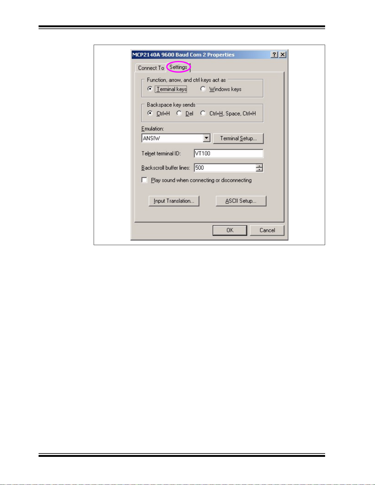
9. In the New Connection Properties window, select the Settings tab. The window
will now look as shown in Figure D-5. Ensure that your settings match the
settings shown.
10. Configure the New Connection Properties Settings.
- Under the “Function, arrow and control keys act as” item, select the
Terminal Keys rad io bu tton.
- Under the “Backspace key sends” item, select the Ctrl+H radio button.
- From the “Emulati on ” pu ll-d ow n me n u, selec t Auto-detect.
- For “Telnet Terminal ID”, enter ANSI.
- For “Backscroll buffer lines”, select 500 from the pull-down menu.
11. Press the ASCII Setup button. This will open the ASCII Setup window
(Figure D-5).
DS51869A-page 54 © 2009 Microchip Technology Inc.
Page 55

Configuring the HyperTerminal® Program
12. In the ASCII Sending area of the window:
- Check “Send Line ends with line feeds”.
- Check “Echo typed characters locally”.
- Set the “Line Delay” and the “Character Delay” to ‘0’ milliseconds.
13. In the ASCII Receiving area of the window:
- Uncheck “Append line feeds to incoming line ends”.
- Uncheck “Force incoming data to 7-bit ASCII”.
- Check “Wrap lines that exceed terminal width”.
14. Ensure that your settings match the settings shown.
15. Select the OK button. This closes the ASCII Setup window and returns focus to
the New Connection Properties window.
FIGURE D-5: NEW CONNECTION PROPERTIES - ASCII SETUP
© 2009 Microchip Technology Inc. DS51869A-page 55
Page 56

MCP2150 Developer’s Board User’s Guide
16. In the New Connection Properties window, select the Input Translation button.
This will open the Host System Encoding Method window (Figure D-6).
- In the “Host System Encoding Method” window, select Shift-JIS and click
the OK button to close the window.
17. Then, click the OK button in the New Connection Properties window.
18. Now that all the settings are configured, in HyperTerminal’s pull-down menu,
select File>Save As.
configuration with a name that you can remember (one for the Primary Device
and the other for the Secondary Device).
FIGURE D-6: NEW CONNECTION PROPERTIES - HOST SYSTEM ENCODING METHOD
Select the name that you wish. You may wish to save each
DS51869A-page 56 © 2009 Microchip Technology Inc.
Page 57

Configuring the HyperTerminal® Program
D.1.3 HyperTerminal Configuration for the Secondary Device
This configuration connects the HyperTerminal window to the selected PC’s Serial Port
(for example COM 2), which then can communicate to th e Embedded Syste m (via the
MCP2150 Developer’s Board DB-9 interface).
Figure D-7 through Figure D-10 show the HyperTerminal configuration for the PC
Serial Port connection to the MCP2150’s DB-9 inteface.
Figure D-7 shows the selected COM port to connect to and the configuration of that
COM port (9600 baud, 8-bits, 1 stop bit, no parity, with hardware flow control). The
COM port for your system may need to be different.
1. Clicking on the Settings tab displays the window shown in Figure D-8.
FIGURE D-7: NEW CONNECTION PROPERTIES - PORT CONFIGURATION
© 2009 Microchip Technology Inc. DS51869A-page 57
Page 58
MCP2150 Developer’s Board User’s Guide
FIGURE D-8: NEW CONNECTION PROPERTIES - PORT SETTINGS
DS51869A-page 58 © 2009 Microchip Technology Inc.
Page 59

Configuring the HyperTerminal® Program
2. Clicking on the Input Translation button displays the window shown in
Figure D-9, while clicking on the ASCII Setup button displays the window shown
in Figure D-10.
FIGURE D-9: NEW CONNECTION PROPERTIES - INPUT TRANSLATION
© 2009 Microchip Technology Inc. DS51869A-page 59
Page 60

MCP2150 Developer’s Board User’s Guide
FIGURE D-10: NEW CONNECTION PROPERTIES - ASCII SETUP
DS51869A-page 60 © 2009 Microchip Technology Inc.
Page 61

MCP2150 DEVELOPER’S BOARD
Appendix E. Continuously Transmitted Data Table
E.1 DATA TABLE FOR DEMO #2
Figure E-1 shows the data table that is streamed to the Primary Device after a data byte
has been received. After the 250 bytes have been transmitted, the progr am returns to
the top of the table. This table is streamed continuously until the IR link is closed.
FIGURE E-1: CONTINUOUSLY TRANSMITTED DATA TABLE
"12345678", 0x0D, 0x0A ; 10 Characters - 10
"2BCDEFGH", 0x0D, 0x0A ; 10 Characters - 20
"32345678", 0x0D, 0x0A ; 10 Characters - 30
"4bcdefgh", 0x0D, 0x0A ; 10 Characters - 40
"52345678", 0x0D, 0x0A ; 10 Characters - 50
"6BCDEFGH", 0x0D, 0x0A ; 10 Characters - 60
"72345678", 0x0D, 0x0A ; 10 Characters - 70
"8bcdefgh", 0x0D, 0x0A ; 10 Characters - 80
"92345678", 0x0D, 0x0A ; 10 Characters - 90
"ABCDEFGH", 0x0D, 0x0A ; 10 Characters - 100
"B2345678", 0x0D, 0x0A ; 10 Characters - 110
"Cbcdefgh", 0x0D, 0x0A ; 10 Characters - 120
"D2345678", 0x0D, 0x0A ; 10 Characters - 130
"EBCDEFGH", 0x0D, 0x0A ; 10 Characters - 140
"F2345678", 0x0D, 0x0A ; 10 Characters - 150
"1bcdefgh", 0x0D, 0x0A ; 10 Characters - 160
"22345678", 0x0D, 0x0A ; 10 Characters - 170
"3BCDEFGH", 0x0D, 0x0A ; 10 Characters - 180
"42345678", 0x0D, 0x0A ; 10 Characters - 190
"5bcdefgh", 0x0D, 0x0A ; 10 Characters - 200
"62345678", 0x0D, 0x0A ; 10 Characters - 210
"7BCDEFGH", 0x0D, 0x0A ; 10 Characters - 220
"82345678", 0x0D, 0x0A ; 10 Characters - 230
"9bcdefgh", 0x0D, 0x0A ; 10 Characters - 240
"a2345678", 0x0D, 0x0A ; 10 Characters - 250
USER ’S GUIDE
NOTE: 0x0D = Carriage Return, 0x0A = Line Feed
© 2009 Microchip Technology Inc. DS51869A-page 61
Page 62

MCP2150 Developer’s Board User’s Guide
NOTES:
DS51869A-page 62 © 2009 Microchip Technology Inc.
Page 63

MCP2150 DEVELOPER’S BOARD
MCP2150 Developer’s Board
1
MPLAB
¬
Program Window
RJ-11 to ICSP Cable
ICD 2
USB Cable
Side View
1
Monitor
PC
Appendix F. Programming the MCP2150DM
Note: The MCP2150DM is shipped with the default demonstration firmware
programmed into the PIC18F65J50.
The user may reprogram the PIC18F65J50 with their application firmware or the
supplied demo firmware.
The Programming will require the following items
• 1 PC USB port for programming
• 1 MPLAB ICD 2 module (with USB cable)
• 1 RJ-11 to ICSP Adapter (AC164110)
• CD with .HEX file to program into device (00265.HEX)
Figure F-1 shows a high level block diagram for programming the MCP2150
Developer’s Board. How to program is described in the appropriate MPLAB-IDE and
MPLAB-ICD2 documentation.
FIGURE F-1: PROGRAMMING BLOCK DIAGRAM
USER ’S GUIDE
SYSTEM HARDWARE REQUIREMENTS
Qty Hardware Purpose
1 PC with one USB port To run MPLAB-IDE and communicate to the ICD or ICE hardware.
1 ICD2, ICD3, or Real ICE To program the MCP2150 Developer’s Board PIC18F65J50 device.
1 RJ-11 to ICSP Adapter
(AC164110)
— MCP2150 Developer’s
Board
© 2009 Microchip Technology Inc. DS51869A-page 63
Converts RJ-11 connector of ICD 2 to pins to use for programming the
PICkit interface on the MCP2150 Developer’s Board.
The board to program.
Page 64

WORLDWIDE SALES AND SERVICE
AMERICAS
Corporate Office
2355 West Chandler Blvd.
Chandler, AZ 85224-6199
Tel: 480-792-7200
Fax: 480-792-7277
Technical Support:
http://support.microchip.com
Web Address:
www.microchip.com
Atlanta
Duluth, GA
Tel: 678-957-9614
Fax: 678-957-1455
Boston
Westborough, MA
Tel: 774-760-0087
Fax: 774-760-0088
Chicago
Itasca, IL
Tel: 630-285-0071
Fax: 630-285-0075
Cleveland
Independence, OH
Tel: 216-447-0464
Fax: 216-447-0643
Dallas
Addison, TX
Tel: 972-818-7423
Fax: 972-818-2924
Detroit
Farmington Hills, MI
Tel: 248-538-2250
Fax: 248-538-2260
Kokomo
Kokomo, IN
Tel: 765-864-8360
Fax: 765-864-8387
Los Angeles
Mission Viejo, CA
Tel: 949-462-9523
Fax: 949-462-9608
Santa Clara
Santa Clara, CA
Tel: 408-961-6444
Fax: 408-961-6445
Toronto
Mississauga, Ontario,
Canada
Tel: 905-673-0699
Fax: 905-673-6509
ASIA/PACIFIC
Asia Pacific Office
Suites 3707-14, 37th Floor
Tower 6, The Gateway
Harbour City, Kowloon
Hong Kong
Tel: 852-2401-1200
Fax: 852-2401-3431
Australia - Sydney
Tel: 61-2-9868-6733
Fax: 61-2-9868-6755
China - Beijing
Tel: 86-10-8528-2100
Fax: 86-10-8528-2104
China - Chengdu
Tel: 86-28-8665-5511
Fax: 86-28-8665-7889
China - Hong Kong SAR
Tel: 852-2401-1200
Fax: 852-2401-3431
China - Nanjing
Tel: 86-25-8473-2460
Fax: 86-25-8473-2470
China - Qingdao
Tel: 86-532-8502-7355
Fax: 86-532-8502-7205
China - Shanghai
Tel: 86-21-5407-5533
Fax: 86-21-5407-5066
China - Shenyang
Tel: 86-24-2334-2829
Fax: 86-24-2334-2393
China - Shenzhen
Tel: 86-755-8203-2660
Fax: 86-755-8203-1760
China - Wuhan
Tel: 86-27-5980-5300
Fax: 86-27-5980-5118
China - Xiamen
Tel: 86-592-2388138
Fax: 86-592-2388130
China - Xian
Tel: 86-29-8833-7252
Fax: 86-29-8833-7256
China - Zhuhai
Tel: 86-756-3210040
Fax: 86-756-3210049
ASIA/PACIFIC
India - Bangalore
Tel: 91-80-3090-4444
Fax: 91-80-3090-4080
India - New Delhi
Tel: 91-11-4160-8631
Fax: 91-11-4160-8632
India - Pune
Tel: 91-20-2566-1512
Fax: 91-20-2566-1513
Japan - Yokohama
Tel: 81-45-471- 6166
Fax: 81-45-471-6122
Korea - Daegu
Tel: 82-53-744-4301
Fax: 82-53-744-4302
Korea - Seoul
Tel: 82-2-554-7200
Fax: 82-2-558-5932 or
82-2-558-5934
Malaysia - Kuala Lumpur
Tel: 60-3-6201-9857
Fax: 60-3-6201-9859
Malaysia - Penang
Tel: 60-4-227-8870
Fax: 60-4-227-4068
Philippines - Manila
Tel: 63-2-634-9065
Fax: 63-2-634-9069
Singapore
Tel: 65-6334-8870
Fax: 65-6334-8850
Taiwan - Hsin Chu
Tel: 886-3-6578-300
Fax: 886-3-6578-370
Taiwan - Kaohsiung
Tel: 886-7-536-4818
Fax: 886-7-536-4803
Taiwan - Taipei
Tel: 886-2-2500-6610
Fax: 886-2-2508-0102
Thailand - Bangkok
Tel: 66-2-694-1351
Fax: 66-2-694-1350
EUROPE
Austria - Wels
Tel: 43-7242-2244-39
Fax: 43-7242-2244-393
Denmark - Copenhagen
Tel: 45-4450-2828
Fax: 45-4485-2829
France - Paris
Tel: 33-1-69-53-63-20
Fax: 33-1-69-30-90-79
Germany - Munich
Tel: 49-89-627-144-0
Fax: 49-89-627-144-44
Italy - Milan
Tel: 39-0331-742611
Fax: 39-0331-466781
Netherlands - Drunen
Tel: 31-416-690399
Fax: 31-416-690340
Spain - Madrid
Tel: 34-91-708-08-90
Fax: 34-91-708-08-91
UK - Wokingham
Tel: 44-118-921-5869
Fax: 44-118-921-5820
03/26/09
DS51869A-page 64 © 2009 Microchip Technology Inc.
 Loading...