

Microchip Technology MCP1256 Charge Pump Evaluation Board, MCP1257 Charge Pump Evaluation Board, MCP1258 Charge Pump Evaluation Board, MCP1259 Charge Pump Evaluation Board User guide
Page 1
MCP1256/7/8/9
Charge Pump Evaluation Board
User’s Guide
© 2006 Microchip Technology Inc. DS51603A
Page 2
Note the following details of the code protection feature on Microchip devices:
• Microchip products meet the specification contained in their particular Microchip Data Sheet.
• Microchip believes that its family of products is one of the most secure families of its kind on the market today, when used in the
intended manner and under normal conditions.
• There are dishonest and possibly illegal methods used to breach the code protection feature. All of these methods, to our
knowledge, require using the Microchip products in a manner outside the operating specifications contained in Microchip’s Data
Sheets. Most likely, the person doing so is engaged in theft of intellectual property.
• Microchip is willing to work with the customer who is concerned about the integrity of their code.
• Neither Microchip nor any other semiconductor manufacturer can guarantee the security of their code. Code protection does not
mean that we are guaranteeing the product as “unbreakable.”
Code protection is constantly evolving. We at Microchip are committed to continuously improving the code protection features of our
products. Attempts to break Microchip’s code protection feature may be a violation of the Digital Millennium Copyright Act. If such acts
allow unauthorized access to your software or other copyrighted work, you may have a right to sue for relief under that Act.
Information contained in this publication regarding device
applications and the like is provided only for your convenience
and may be superseded by updates. It is your responsibility to
ensure that your application meets with your specifications.
MICROCHIP MAKES NO REPRESENTATIONS OR WARRANTIES OF ANY KIND WHETHER EXPRESS OR IMPLIED,
WRITTEN OR ORAL, STATUTORY OR OTHERWISE,
RELATED TO THE INFORMATION, INCLUDING BUT NOT
LIMITED TO ITS CONDITION, QUALITY, PERFORMANCE,
MERCHANTABILITY OR FITNESS FOR PURPOSE.
Microchip disclaims all liability arising from this information and
its use. Use of Microchip devices in life support and/or safety
applications is entirely at the buyer’s risk, and the buyer agrees
to defend, indemnify and hold harmless Microchip from any and
all damages, claims, suits, or expenses resulting from such
use. No licenses are conveyed, implicitly or otherwise, under
any Microchip intellectual property rights.
Trademarks
The Microchip name and logo, the Microchip logo, Accuron,
dsPIC, K
EELOQ, microID, MPLAB, PIC, PICmicro,
PICSTART, PRO MATE, PowerSmart, rfPIC and SmartShunt
are registered trademarks of Microchip Technology
Incorporated in the U.S.A. and other countries.
AmpLab, FilterLab, Migratable Memory, MXDEV, MXLAB,
PICMASTER, SEEVAL, SmartSensor and The Embedded
Control Solutions Company are registered trademarks of
Microchip Technology Incorporated in the U.S.A.
Analog-for-the-Digital Age, Application Maestro, dsPICDEM,
dsPICDEM.net, dsPICworks, ECAN, ECONOMONITOR,
FanSense, FlexROM, fuzzyLAB, In-Circuit Serial
Programming, ICSP, ICEPIC, Linear Active Thermistor,
MPASM, MPLIB, MPLINK, MPSIM, PICkit, PICDEM,
PICDEM.net, PICLAB, PICtail, PowerCal, PowerInfo,
PowerMate, PowerTool, Real ICE, rfLAB, rfPICDEM, Select
Mode, Smart Serial, SmartTel, Total Endurance, UNI/O,
WiperLock and Zena are trademarks of Microchip Technology
Incorporated in the U.S.A. and other countries.
SQTP is a service mark of Microchip Technology Incorporated
in the U.S.A.
All other trademarks mentioned herein are property of their
respective companies.
© 2006, Microchip Technology Incorporated, Printed in the
U.S.A., All Rights Reserved.
Printed on recycled paper.
Microchip received ISO/TS-16949:2002 quality system certification for
its worldwide headquarters, design and wafer fabrication facilities in
Chandler and Tempe, Arizona and Mountain View, California in
October 2003. The Company’s quality system processes and
procedures are for its PICmicro
devices, Serial EEPROMs, microperipherals, nonvolatile memory and
analog products. In addition, Microchip’s quality system for the design
and manufacture of development systems is ISO 9001:2000 certified.
®
8-bit MCUs, KEELOQ
®
code hopping
DS51603A-page ii © 2006 Microchip Technology Inc.
Page 3
MCP1256/7/8/9 CHARGE PUMP
EVALUATION BOARD USER’S GUIDE
Table of Contents
Preface ........................................................................................................................... 1
Chapter 1. Product Overview ....................................................................................... 5
1.1 Introduction ..................................................................................................... 5
1.2 What is the MCP1256/7/8/9 Charge Pump Evaluation Board? ...................... 6
1.3 What the MCP1256/7/8/9 Charge Pump Evaluation Board Includes ............. 6
Chapter 2. Installation and Operation ......................................................................... 7
2.1 Introduction ..................................................................................................... 7
2.2 Features ......................................................................................................... 7
2.3 Getting Started ............................................................................................... 8
Appendix A. Schematic and Layouts ........................................................................ 11
A.1 Introduction .................................................................................................. 11
A.2 Board Schematic ...................................................................................... 12
A.3 Board - Assembly Drawing ....................................................................... 13
A.4 Board - Top Overlay ................................................................................. 14
A.5 Board - Top Layer .................................................................................... 15
A.6 Board - Bottom Layer ............................................................................... 16
Appendix B. Bill Of Materials (BOM) ......................................................................... 17
Worldwide Sales and Service .................................................................................... 18
© 2006 Microchip Technology Inc. DS51603A-page iii
Page 4

MCP1256/7/8/9 Charge Pump Evaluation Board User’s Guide
NOTES:
DS51603A-page iv © 2006 Microchip Technology Inc.
Page 5
MCP1256/7/8/9 CHARGE PUMP
EVALUATION BOARD USER’S GUIDE
Preface
NOTICE TO CUSTOMERS
All documentation becomes dated, and this manual is no exception. Microchip tools and
documentation are constantly evolving to meet customer needs, so some actual dialogs
and/or tool descriptions may differ from those in this document. Please refer to our web site
(www.microchip.com) to obtain the latest documentation available.
Documents are identified with a “DS” number. This number is located on the bottom of each
page, in front of the page number. The numbering convention for the DS number is
“DSXXXXXA”, where “XXXXX” is the document number and “A” is the revision level of the
document.
For the most up-to-date information on development tools, see the MPLAB
Select the Help menu, and then Topics to open a list of available on-line help files.
®
IDE on-line help.
INTRODUCTION
This chapter contains general information that will be useful to know before using the
MCP1256/7/8/9 Charge Pump Evaluation Board. Items discussed in this chapter
include:
• Document Layout
• Conventions Used in this Guide
• Recommended Reading
• The Microchip Web Site
• Customer Support
• Document Revision History
DOCUMENT LAYOUT
This document describes how to use the MCP1256/7/8/9 Charge Pump Evaluation
Board. The manual layout is as follows:
• Chapter 1. “Product Overview” – Important information about the
MCP1256/7/8/9 Charge Pump Evaluation Board.
• Chapter 2. “Installation and Operation” – Includes instructions on how to get
started and a description of the MCP1256/7/8/9 Charge Pump Evaluation Board.
• Appendix A. “Schematic and Layouts” – Shows the schematic and board lay-
out diagram for the MCP1256/7/8/9 Charge Pump Evaluation Board.
• Appendix B. “Bill Of Materials (BOM)” – Lists the parts used to build the
MCP1256/7/8/9 Charge Pump Evaluation Board.
© 2006 Microchip Technology Inc. DS51603A-page 1
Page 6
MCP1256/7/8/9 Charge Pump Evaluation Board User’s Guide
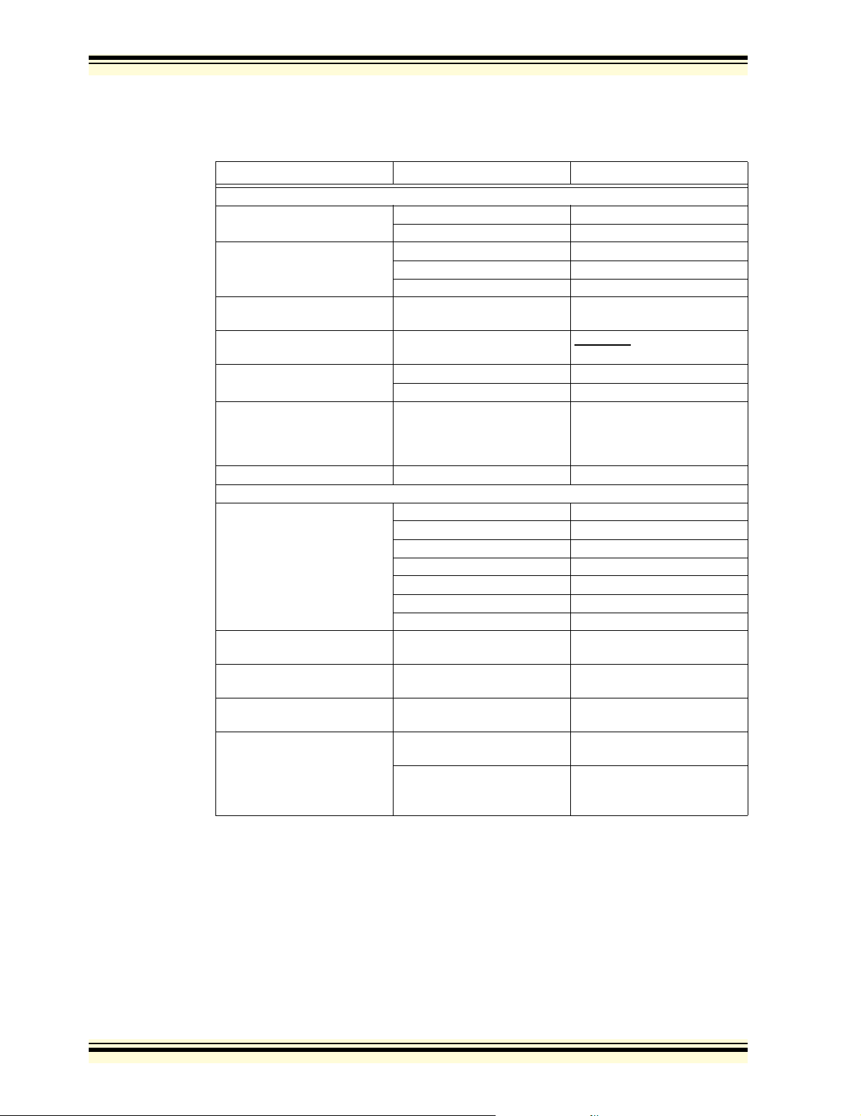
CONVENTIONS USED IN THIS GUIDE
This manual uses the following documentation conventions:
DOCUMENTATION CONVENTIONS
Description Represents Examples
Arial font:
Italic characters Referenced books MPLAB
Emphasized text ...is the only compiler...
Initial caps A window the Output window
A dialog the Settings dialog
A menu selection select Enable Programmer
Quotes A field name in a window or
dialog
Underlined, italic text with
right angle bracket
Bold characters A dialog button Click OK
N‘Rnnnn A number in verilog format,
Text in angle brackets < > A key on the keyboard Press <Enter>, <F1>
Courier New font:
Plain Courier New Sample source code #define START
Italic Courier New A variable argument file.o, where file can be
Square brackets [ ] Optional arguments mcc18 [options] file
Curly brackets and pipe
character: { | }
Ellipses... Replaces repeated text var_name [,
A menu path File>Save
A tab Click the Power tab
where N is the total number of
digits, R is the radix and n is a
digit.
Filenames autoexec.bat
File paths c:\mcc18\h
Keywords _asm, _endasm, static
Command-line options -Opa+, -Opa-
Bit values 0, 1
Constants 0xFF, ‘A’
Choice of mutually exclusive
arguments; an OR selection
Represents code supplied by
user
“Save project before build”
4‘b0010, 2‘hF1
any valid filename
[options]
errorlevel {0|1}
var_name...]
void main (void)
{ ...
}
®
IDE User’s Guide
RECOMMENDED READING
This user's guide describes how to use the MCP1256/7/8/9 Charge Pump Evaluation
Board. Other useful documents are listed below. The following Microchip documents
are available and recommended as supplemental reference resources.
MCP1256/7/8/9 Data Sheet, “Regulated 3.3V, Low-Ripple Charge Pump with
Low-Operating Current SLEEP Mode or BYPASS Mode” (DS21989)
This data sheet provides detailed information regarding the MCP1256/7/8/9 product
family.
DS51603A-page 2 © 2006 Microchip Technology Inc.
Page 7

THE MICROCHIP WEB SITE
Microchip provides online support via our web site at www.microchip.com. This web
site is used as a means to make files and information easily available to customers.
Accessible by using your favorite Internet browser, the web site contains the following
information:
• Product Support – Data sheets and errata, application notes and sample
programs, design resources, user’s guides and hardware support documents,
latest software releases and archived software
• General Technical Support – Frequently Asked Questions (FAQs), technical
support requests, online discussion groups, Microchip consultant program
member listing
• Business of Microchip – Product selector and ordering guides, latest Microchip
press releases, listing of seminars and events, listings of Microchip sales offices,
distributors and factory representatives
CUSTOMER SUPPORT
Users of Microchip products can receive assistance through several channels:
• Distributor or Representative
• Local Sales Office
• Field Application Engineer (FAE)
• Technical Support
• Development Systems Information Line
Customers should contact their distributor, representative or field application engineer
(FAE) for support. Local sales offices are also available to help customers. A listing of
sales offices and locations is included in the back of this document.
Technical support is available through the web site at: http://support.microchip.com
Preface
DOCUMENT REVISION HISTORY
Revision A (March 2006)
• Initial Release of this Document.
© 2006 Microchip Technology Inc. DS51603A-page 3
Page 8

MCP1256/7/8/9 Charge Pump Evaluation Board User’s Guide
NOTES:
DS51603A-page 4 © 2006 Microchip Technology Inc.
Page 9

Chapter 1. Product Overview
1.1 INTRODUCTION
The MCP1256/7/8/9 Charge Pump Evaluation Board is used to evaluate Microchip’s
MCP1256/7/8/9 Regulated 3.3V, Low-Ripple Charge Pumps with low-operating current
SLEEP mode or BYPASS mode.
This chapter covers the following topics:
• What is the MCP1256/7/8/9 Charge Pump Evaluation Board?
• What the MCP1256/7/8/9 Charge Pump Evaluation Board Includes
MCP1256/7/8/9 CHARGE PUMP
EVALUATION BOARD USER’S GUIDE
INPUT
1.6V to 3.6V
INPUT
1.6V to 3.6V
C
IN
10 μF
C
IN
10 μF
ON / OFF
MCP1256
V
OUT
C2+
C2-
OUT
LBO
C2+
C2-
5
1
6
3
5
1
6
3
7
V
IN
10
SHDN
4
10
8
2
7
4
8
C1+
C1-
SLEEP
V
IN
SHDN
C1+
C1-
C
1
1 μF
Typical Application with Power-Good Indication
C
1
1 μF
V
PGOOD
GND
9
MCP1259
R
1
C
2
1 μF
R
1
C
2
1 μF
OUTPUT
3.3V
C
OUT
10 μF
Power-Good
Indication
OUTPUT
3.3V
C
OUT
10 μF
Low-Battery
Indication
2
BYPASS
ON / OFF
Typical Application with Low-Battery Indication
GND
9
FIGURE 1-1: Typical MCP1256/7/8/9 Applications.
© 2006 Microchip Technology Inc. DS51603A-page 5
Page 10

MCP1256/7/8/9 Charge Pump Evaluation Board User’s Guide
1.2 WHAT IS THE MCP1256/7/8/9 CHARGE PUMP EVALUATION BOARD?
The MCP1256/7/8/9 Charge Pump Evaluation Board is an evaluation and demonstration
tool for Microchip Technology’s MCP1256/7/8/9 Regulated 3.3V, Low-Ripple Charge Pumps with
low-operating current SLEEP mode or BYPASS mode. The design provides for dynamic
versatility.
The MCP1256/7/8/9 Charge Pump Evaluation Board is setup to evaluate simple, stand-alone,
DC-to-DC conversion.
of the MCP1256/7/8/9 device family.
demonstrating the SLEEP mode feature along with a power good indication. The other
evaluation circuit utilizes the MCP1259, demonstrating the unique BYPASS mode feature, along
with a low battery indication.
When connected, the MCP1256/7/8/9 devices can be evaluated in a variety of applications.
1.3 WHAT THE MCP1256/7/8/9 CHARGE PUMP EVALUATION BOARD
INCLUDES
This MCP1256/7/8/9 Charge Pump Evaluation Board includes:
• MCP1256/7/8/9 Charge Pump Evaluation Board, 102-00099
• MCP1256/7/8/9 Charge Pump Evaluation Board User’s Guide, DS51603
• MCP1256/7/8/9 Data Sheet, “Regulated 3.3V, Low-Ripple Charge Pump with
Low-Operating Current SLEEP Mode or BYPASS Mode”, DS21989
Two evaluation circuits are provided, demonstrating the versatility
One evaluation circuit utilizes the MCP1256,
DS51603A-page 6 © 2006 Microchip Technology Inc.
Page 11

Chapter 2. Installation and Operation
2.1 INTRODUCTION
The MCP1256/7/8/9 Charge Pump Evaluation Board demonstrates Microchip’s
MCP1256/7/8/9 devices. The MCP1256/7/8/9 devices are positive regulated charge
pumps that accept an input voltage from +1.8V to +3.6V and convert it to a regulated
3.3V output voltage. The MCP1256/7/8/9 provide a low-cost, compact and simple
solution for step-up DC/DC conversions, primarily in battery applications that do not
want to use switching regulator solutions because of EMI noise and inductor size.
The MCP1256/7/8/9 are designed to offer the highest possible efficiency under
common operating conditions, i.e. V
fixed switching frequency, 650 kHz (typically), allows for easy external filtering.
The MCP1256/7 provide a unique SLEEP mode feature. SLEEP mode reduces the
current drawn from the input supply while maintaining a regulated bias on external
peripherals. SLEEP mode can substantially increase battery run-time in portable
applications.
The MCP1258/9 provide a unique BYPASS mode feature. BYPASS virtually eliminates
the current drawn from the input supply by the device, while maintaining an unregulated
bias on external peripherals. BYPASS connects the input supply voltage to the output.
All remaining functions of the device are shutdown. BYPASS mode can substantially
increase battery run-time in portable applications.
The devices supply up to 100 mA of output current for input voltages, V
or equal to 2.2V.
MCP1256/7/8/9 CHARGE PUMP
EVALUATION BOARD USER’S GUIDE
= 2.4V or 2.8V, V
IN
OUT
= 3.3V, I
= 100 mA. A
OUT
, greater than
IN
2.2 FEATURES
The MCP1256/7/8/9 Charge Pump Evaluation Board is used to evaluate various device
options. Two evaluation circuits are provided as a guide to external component
selection and board layout. Emphasis has been placed on cost, board area, thermal
management and performance. One evaluation circuit utilizes the MCP1256,
demonstrating the SLEEP mode feature along with a power good indication. The other
evaluation circuit utilizes the MCP1259 demonstrating the unique BYPASS mode
feature along with a low-battery indication.
The MCP1256/7/8/9 Charge Pump Evaluation Board has the following features:
• Evaluation of the MCP1256 in a 10-pin MSOP package
• Evaluation of the MCP1259 in a 10-pin MSOP package
• Simple, stand-alone operation
• Powered from external bench supply or compatible battery input
• Surface-mount design
• Fully assembled and tested
© 2006 Microchip Technology Inc. DS51603A-page 7
Page 12

MCP1256/7/8/9 Charge Pump Evaluation Board User’s Guide
C5
R4
C1
R1
C6
R6
C2
R3
U2
TP 9 TP 10
TP 5
U1
TP 2 TP 3
C7 C8
R5
TP 12
TP 14
C3 C4
R2
TP 7
TP 8
TP 4
TP 1
TP 11
TP 13
TP 6
2.3 GETTING STARTED
The MCP1256/7/8/9 Evaluation Board is fully assembled and tested for generating a
regulated 3.3V output voltage from a 1.8V to 3.6V input at load currents up to 100 mA.
The board requires the use of an external input voltage source and external load.
2.3.1 Power Input and Output Connections
2.3.1.1 POWERING THE MCP1256/7/8/9 EVALUATION BOARD
1. Apply the input voltage source to the appropriate circuit for evaluation. The input
voltage source should be limited to the 0V to +3.6V range. For normal operation,
the input voltage should be between +1.8V and +3.6V. The input voltage must
not exceed an absolute maximum of +3.8V.
2. Connect the positive side of the input source (+) to V
evaluated. Connect the negative or return side of the input source (-) to GND of
the circuit being evaluated. Refer to Figure 2-1.
of the circuit being
IN
Output
Load
Output
Load
_
+
_
+
_
Input
Power Supply
+
1.8V to 3.6V
_
Input
Power Supply
+
1.8V to 3.6V
FIGURE 2-1: Setup Configuration Diagram.
2.3.1.2 APPLYING THE LOAD TO THE MCP1256/7/8/9 EVALUATION BOARD
1. To apply a load to a MCP1256/7/8/9 Evaluation Board, the positive side of the
load (+) should be connected to V
2. The negative or return side of the load (-) should be connected to GND of the
circuit being evaluated. Care should be taken when using electronic loads or
ground referenced loads.
of the circuit being evaluated.
OUT
DS51603A-page 8 © 2006 Microchip Technology Inc.
Page 13

Installation and Operation
2.3.2 Shutdown Mode (SHDN)
Driving SHDN low puts the MCP1256/7/8/9 in a low-power Shutdown mode. This
disables the charge-pump switches, oscillator and control logic, reducing the quiescent
current to 0.1 μA (typical). The PGOOD output and LBO
during shutdown.
2.3.3 SLEEP Mode (SLEEP)
The MCP1256/7 provide a unique SLEEP mode feature. SLEEP mode reduces the
current drawn from the input supply, while maintaining a regulated bias on external
peripherals. SLEEP mode can substantially increase battery run-time in portable
applications.
The regulation control is hysteretic, otherwise referred to as a bang-bang control. The
output is regulated around a fixed reference with some hysteresis. As a result, some
amount of peak-to-peak ripple will be observed at the output independent of load
current. The frequency of the output ripple, however, will be influenced heavily by the
load current and output capacitance.
2.3.4 BYPASS Mode (BYPASS)
The MCP1258/9 provide a unique BYPASS mode feature. BYPASS virtually eliminates
the current drawn from the input supply by the device, while maintaining an unregulated
bias on external peripherals. BYPASS connects the input supply voltage to the output.
All remaining functions of the device are shutdown. BYPASS mode can substantially
increase battery run-time in portable applications.
are in a high impedance state
2.3.5 Device Support Options
The MCP1256/7/8/9 Charge Pump Evaluation Board supports the entire
MCP1256/7/8/9 family. The MCP1256/7/8/9 Charge Pump Evaluation Board is
provided with two evaluation circuits utilizing the MCP1256 and MCP1259. Alternate
devices can be substituted in order to evaluate the different MCP1256/7/8/9 family
options.
© 2006 Microchip Technology Inc. DS51603A-page 9
Page 14

MCP1256/7/8/9 Charge Pump Evaluation Board User’s Guide
NOTES:
DS51603A-page 10 © 2006 Microchip Technology Inc.
Page 15

Appendix A. Schematic and Layouts
A.1 INTRODUCTION
This appendix contains the following schematic and layouts for the MCP1256/7/8/9
Charge Pump Evaluation Board.
Diagrams included in this appendix:
• Board Schematic
• Board - Assembly Drawing
• Board - Top Overlay
• Board - Top Layer
• Board - Bottom Layer
MCP1256/7/8/9 CHARGE PUMP
EVALUATION BOARD USER’S GUIDE
© 2006 Microchip Technology Inc. DS51603A-page 11
Page 16

MCP1256/7/8/9 Charge Pump Evaluation Board User’s Guide
A.2 BOARD SCHEMATIC
DS51603A-page 12 © 2006 Microchip Technology Inc.
Page 17

A.3 BOARD - ASSEMBLY DRAWING
C5
R4
C1
R1
C6
R6
C2
R3
U2
TP9 TP10
TP5
U1
TP2 TP3
C7 C8
R5
TP12
TP14
C3 C4
R2
TP7
TP8
TP4
TP1
TP11
TP13
TP6
Schematic and Layouts
© 2006 Microchip Technology Inc. DS51603A-page 13
Page 18

MCP1256/7/8/9 Charge Pump Evaluation Board User’s Guide
C5
R4
C1
R1
C6
R6
C2
R3
U2
TP 9 TP 10
TP 5
U1
TP 2 TP 3
C7 C8
R5
TP 12
TP 14
C3 C4
R2
TP 7
TP 8
TP 4
TP 1
TP 11
TP 13
TP 6
A.4 BOARD - TOP OVERLAY
DS51603A-page 14 © 2006 Microchip Technology Inc.
Page 19

A.5 BOARD - TOP LAYER
Schematic and Layouts
© 2006 Microchip Technology Inc. DS51603A-page 15
Page 20

MCP1256/7/8/9 Charge Pump Evaluation Board User’s Guide
A.6 BOARD - BOTTOM LAYER
DS51603A-page 16 © 2006 Microchip Technology Inc.
Page 21

MCP1256/7/8/9 CHARGE PUMP
EVALUATION BOARD USER’S GUIDE
Appendix B. Bill Of Materials (BOM)
TABLE B-1: BILL OF MATERIALS (BOM)
Qty. Reference Description Mfgr. Part Number
4 C1,C2,C5,C6 10uF, X5R Ceramic, 10V, 1206 Taiyo Yuden
4 C3,C4,C7,C8 1uF, X7R Ceramic, 16V, 0603 Taiyo Yuden EMK107BJ105KA-TR
6 R1,R2,R3,R4,R5,R6 100k, 1/10W, Chip Resistor, 0603 Panasonic
12 TP1-TP12 Surface Mount Test Point, 5016 Keystone
1 U1 Positive Regulated Charge Pump,
MSOP10
1 U2 Positive Regulated Charge Pump,
MSOP10
4 — Bump-ons 3M SJ5003
1 — Printed Circuit Board Advanced Circuits 104-00099-R1
Microchip Technology,
Inc.
Microchip Technology,
Inc.
®
®
-ECG ERJ-3EK1003V
®
Electronics 5016
LMK316BJ106KL-T
MCP1256-I/MS
MCP1259-I/MS
© 2006 Microchip Technology Inc. Draft DS51603A-page 17
Page 22

WORLDWIDE SALES AND SERVICE
AMERICAS
Corporate Office
2355 West Chandler Blvd.
Chandler, AZ 85224-6199
Tel: 480-792-7200
Fax: 480-792-7277
Technical Support:
http://support.microchip.com
Web Address:
www.microchip.com
Atlanta
Alpharetta, GA
Tel: 770-640-0034
Fax: 770-640-0307
Boston
Westborough, MA
Tel: 774-760-0087
Fax: 774-760-0088
Chicago
Itasca, IL
Tel: 630-285-0071
Fax: 630-285-0075
Dallas
Addison, TX
Tel: 972-818-7423
Fax: 972-818-2924
Detroit
Farmington Hills, MI
Tel: 248-538-2250
Fax: 248-538-2260
Kokomo
Kokomo, IN
Tel: 765-864-8360
Fax: 765-864-8387
Los Angeles
Mission Viejo, CA
Tel: 949-462-9523
Fax: 949-462-9608
San Jose
Mountain View, CA
Tel: 650-215-1444
Fax: 650-961-0286
Toronto
Mississauga, Ontario,
Canada
Tel: 905-673-0699
Fax: 905-673-6509
ASIA/PACIFIC
Australia - Sydney
Tel: 61-2-9868-6733
Fax: 61-2-9868-6755
China - Beijing
Tel: 86-10-8528-2100
Fax: 86-10-8528-2104
China - Chengdu
Tel: 86-28-8676-6200
Fax: 86-28-8676-6599
China - Fuzhou
Tel: 86-591-8750-3506
Fax: 86-591-8750-3521
China - Hong Kong SAR
Tel: 852-2401-1200
Fax: 852-2401-3431
China - Qingdao
Tel: 86-532-8502-7355
Fax: 86-532-8502-7205
China - Shanghai
Tel: 86-21-5407-5533
Fax: 86-21-5407-5066
China - Shenyang
Tel: 86-24-2334-2829
Fax: 86-24-2334-2393
China - Shenzhen
Tel: 86-755-8203-2660
Fax: 86-755-8203-1760
China - Shunde
Tel: 86-757-2839-5507
Fax: 86-757-2839-5571
China - Wuhan
Tel: 86-27-5980-5300
Fax: 86-27-5980-5118
China - Xian
Tel: 86-29-8833-7250
Fax: 86-29-8833-7256
ASIA/PACIFIC
India - Bangalore
Tel: 91-80-4182-8400
Fax: 91-80-4182-8422
India - New Delhi
Tel: 91-11-5160-8631
Fax: 91-11-5160-8632
India - Pune
Tel: 91-20-2566-1512
Fax: 91-20-2566-1513
Japan - Yokohama
Tel: 81-45-471- 6166
Fax: 81-45-471-6122
Korea - Gumi
Tel: 82-54-473-4301
Fax: 82-54-473-4302
Korea - Seoul
Tel: 82-2-554-7200
Fax: 82-2-558-5932 or
82-2-558-5934
Malaysia - Penang
Tel: 60-4-646-8870
Fax: 60-4-646-5086
Philippines - Manila
Tel: 63-2-634-9065
Fax: 63-2-634-9069
Singapore
Tel: 65-6334-8870
Fax: 65-6334-8850
Taiwan - Hsin Chu
Tel: 886-3-572-9526
Fax: 886-3-572-6459
Taiwan - Kaohsiung
Tel: 886-7-536-4818
Fax: 886-7-536-4803
Taiwan - Taipei
Tel: 886-2-2500-6610
Fax: 886-2-2508-0102
Thailand - Bangkok
Tel: 66-2-694-1351
Fax: 66-2-694-1350
EUROPE
Austria - Wels
Tel: 43-7242-2244-399
Fax: 43-7242-2244-393
Denmark - Copenhagen
Tel: 45-4450-2828
Fax: 45-4485-2829
France - Paris
Tel: 33-1-69-53-63-20
Fax: 33-1-69-30-90-79
Germany - Munich
Tel: 49-89-627-144-0
Fax: 49-89-627-144-44
Italy - Milan
Tel: 39-0331-742611
Fax: 39-0331-466781
Netherlands - Drunen
Tel: 31-416-690399
Fax: 31-416-690340
Spain - Madrid
Tel: 34-91-708-08-90
Fax: 34-91-708-08-91
UK - Wokingham
Tel: 44-118-921-5869
Fax: 44-118-921-5820
02/16/06
DS51603A-page 18 © 2006 Microchip Technology Inc.
 Loading...