

Page 1

LIN Serial Analyzer
User’s Guide Rev2.0
© 2008 Microchip Technology Inc. DS51675B
Page 2

Note the following details of the code protection feature on Microchip devices:
• Microchip products meet the specification contained in their particular Microchip Data Sheet.
• Microchip believes that its family of products is one of the most secure families of its kind on the market today, when used in the
intended manner and under normal conditions.
• There are dishonest and possibly illegal methods used to breach the code protection feature. All of these methods, to our
knowledge, require using the Microchip products in a manner outside the operating specifications contained in Microchip’s Data
Sheets. Most likely, the person doing so is engaged in theft of intellectual property.
• Microchip is willing to work with the customer who is concerned about the integrity of their code.
• Neither Microchip nor any other semiconductor manufacturer can guarantee the security of their code. Code protection does not
mean that we are guaranteeing the product as “unbreakable.”
Code protection is constantly evolving. We at Microchip are committed to continuously improving the code protection features of our
products. Attempts to break Microchip’s code protection feature may be a violation of the Digit al Millennium Copyright A ct. If such acts
allow unauthorized access to your software or other copyrighted work, you may have a right to sue for relief under that Act.
Information contained in this publication regarding device
applications and t he lik e is provided only for your convenience
and may be su perseded by upda t es . It is y our responsibility to
ensure that your application meets with your specifications.
MICROCHIP MAKES NO REPRESENTATIONS OR
WARRANTIES OF ANY KIND WHETHER EXPRESS OR
IMPLIED, WRITTEN OR ORAL, STATUTORY OR
OTHERWISE, RELATED TO THE INFORMATION,
INCLUDING BUT NOT LIMITED TO ITS CONDITION,
QUALITY, PERFORMANCE, MERCHANTABILITY OR
FITNESS FOR PURPOSE. Microchip disclaims all liability
arising from this information and its use. Use of Microchip
devices in life supp ort and/or safety ap plications is entir ely at
the buyer’s risk, and the buyer agrees to defend, indemnify and
hold harmless M icrochip from any and all dama ges, claims,
suits, or expenses re sulting from such use. No licens es are
conveyed, implicitly or otherwise, under any Microchip
intellectual property rights.
Trademarks
The Microchip name and logo, the Microchip logo, Accuron,
dsPIC, K
EELOQ, KEELOQ logo, microID, MPLAB, PIC,
PICmicro, PICSTART, PRO MATE, rfPIC and SmartShunt are
registered trademarks of Microchip Technology Incorporated
in the U.S.A. and other countries.
AmpLab, FilterLab, Linear Active Thermistor, Migratable
Memory, MXDEV, MXLAB, SEEVAL, SmartSensor and The
Embedded Control Solutions Company are registered
trademarks of Microchip Technology Incorporated in the
U.S.A.
Analog-for-the-Digital Age, Application Maestro, CodeGuard,
dsPICDEM, dsPICDEM.net, dsPICworks, ECAN,
ECONOMONITOR, FanSense, FlexROM, fuzzyLAB,
In-Circuit Serial Programming, ICSP, ICEPIC, Mindi, MiWi,
MPASM, MPLAB Certified logo, MPLIB, MPLINK, PICkit,
PICDEM, PICDEM.net, PICLAB, PICtail, PowerCal,
PowerInfo, PowerMate, PowerTool, REAL ICE, rfLAB, Select
Mode, Smart Serial, SmartTel, Total Endurance, UNI/O,
WiperLock and ZENA are trademarks of Microchip
Technology Incorporated in the U.S.A. and other countries.
SQTP is a service mark of Microchip Technology Incorporated
in the U.S.A.
All other trademarks mentioned herein are property of their
respective companies.
© 2008, Microchip Technology Incorporated, Printed in the
U.S.A., All Rights Reserved.
Printed on recycled paper.
Microchip received ISO/TS-16949:2002 certification for its worldwide
headquarters, design and wafer fabrication facilities in Chandler and
Tempe, Arizona; Gresham, Oregon and design centers in California
and India. The Company’s quality system processes and procedures
are for its PIC
devices, Serial EEPROMs, microperipherals, nonvolatile memory and
analog products. In addition, Microchip’s quality system for the design
and manufacture of development systems is ISO 9001:2000 certified.
®
MCUs and dsPIC® DSCs, KEELOQ
®
code hopping
DS51675B-page ii © 2008 Microchip Technology Inc.
Page 3

LIN SERIAL ANALYZER
USER ’S GUIDE REV2.0
Table of Contents
Preface ...........................................................................................................................1
Chapter 1. LIN Serial Analyzer Overview.....................................................................5
1.1 Introduction .....................................................................................................5
1.2 Highlight s ......... ............. .. .. ........................... .. .. ........................... .. .. ................ 5
1.3 LIN Serial A n a lyzer Conten ts ......... .......................... .. ... ............. .. .................. 5
1.4 LIN Serial Analyzer Development Tool ..........................................................5
1.5 LIN Serial A n a ly zer Hardware ................ ... .. ............. .. ... ............. .. .. ............. ... 6
1.6 LIN Serial A n a ly zer Software ............. ........................... .. .. ............. .. ... ........... 8
Chapter 2. Getting Started – Quick Setup....................................................................9
2.1 Highlight s ......... ............. .. .. ........................... .. .. ........................... .. .. ................ 9
2.2 Using the LIN S e ria l Analyzer for the F irs t Time ............... ............................. 9
2.3 Software In st a lla tion ............ ............. .. .. ........................... .. .. ........................... 9
2.4 Running L IN S e rial Analyzer P ro g ram ...... .. .......................... ... ............. .. .. ..... 9
Chapter 3. LIN Serial Analyzer PC Program ..............................................................11
3.1 Highlight s ......... ............. .. .. ........................... .. .. ........................... .. .. .............. 11
3.2 Interface Ov e r view .......................................................... .. .. ......................... 11
3.3 Transaction Window .....................................................................................12
3.4 File Functions ...............................................................................................14
3.5 Setup Functions ...........................................................................................16
3.6 Tools Functions ............................................................................................18
3.7 Start/Stop Logging Button ................................................................. ...........19
3.8 Master Message Group Box .........................................................................19
3.9 Status Bar ..................... .. .. ........................... .. .. ........................... .. .. .............. 22
Appendix A. LIN Serial Analyzer Technical Information ..........................................23
A.1 Highlight s .......... .......................... ... .. .......................... ... .. ............................. 2 3
A.2 LIN Serial Ana lyzer Schem a tic ............ .. ........................................ .. ... ......... 23
Index .............................................................................................................................25
Worldwide Sales and Service ....................................................................................27
© 2008 Microchip Technology Inc. DS51675B-page iii
Page 4

LIN Serial Analyzer User’s Guide Rev2.0
NOTES:
DS51675B-page iv © 2008 Microchip Technology Inc.
Page 5

LIN SERIAL ANALYZER
USER ’S GUIDE REV2.0
Preface
NOTICE TO CUSTOMERS
All documentation becomes dated, and this manual is no exception. Microchip tools and
documentation are constantly evolving to meet customer needs, so some actual dialogs
and/or tool descriptions may differ from those in this document. Please refer to our web site
(www.microchip.com) to obtain the latest documentation available.
Documents are identified with a “DS” number. This number is located on the bottom of each
page, in front of the page number. The numbering convention for the DS number is
“DSXXXXXA”, where “XXXXX” is the document number and “A” is the revision level of the
document.
For the most up-to-date information on development tools, see the MPLAB
Select the Help menu, and then Topics to open a list of available on-line help files.
INTRODUCTION
®
IDE on-line help.
This chapter contains general information that will be useful to know before using the
LIN Serial Analyser. Items discussed in this chapter include:
• Document Layout
• Conventions Used in this Guide
• Recommended Reading
• The Microchip Web Site
• Customer Support
• Document Revision History
DOCUMENT LAYOUT
This document describes how to use the LIN Serial Analyser. The manual layout is as
follows:
• Chapter 1. “LIN Serial Analyser Overview” – What the LIN Serial Analyser is,
what makes it a desirable development tool and what features are available.
• Chapter 2. “Getting Started – Quick Setup” – Describes the supplies needed to
set up and begin to use the LIN Serial Analyser.
• Chapter 3. “LIN Serial Analyser PC Program” – Describes the primary
elements of the interface.
• Appendix A. “LIN Serial Analyzer Technical Information” – Provides the
detailed schematic of the LIN Serial Analyser.
© 2008 Microchip Technology Inc. DS51675B-page 1
Page 6
LIN Serial Analyzer User’s Guide Rev2.0
CONVENTIONS USED IN THIS GUIDE
This manual uses the following docum entat io n conven tion s:
DOCUMENTATION CONVENTIONS
Description Represents Examples
Arial font:
Italic characters Referenced books MPLAB
Emphasized text ...is the only comp ile r...
Initial caps A window the Output window
A dialog the Settings dialog
A menu selection select Enable Programmer
Quotes A field name in a window or
dialog
Underlined, italic text with
right angle bracket
Bold characters A dialog button Click OK
N‘Rnnnn A number in verilog format,
Text in angle brackets < > A key on the keyboard Press <Enter>, <F1>
Courier New font:
Plain Courier New Sam ple source code #define START
Italic Courier New A variable argument file.o, where file can be
Square brackets [ ] Optional arguments mcc18 [options] file
Curly brackets and pipe
character: { | }
Ellipses... Replaces r epeated text var_name [,
A menu path File>Save
A tab Click the Power tab
where N is the tota l number of
digits, R is th e radi x and n is a
digit.
File names autoexec.bat
File paths c:\mcc18\h
Keywords _asm, _endasm, static
Command-line options -Opa+, -Opa-
Bit values 0, 1
Constants 0xFF, ‘A’
Choice of mutually exclusive
arguments; an OR selection
Represents code supplied by
user
®
IDE User’s Guide
“Save project before build”
4‘b0010, 2‘hF1
any valid file name
[options]
errorlevel {0|1}
var_name...]
void main (void)
{ ...
}
DS51675B-page 2 © 2008 Microchip Technology Inc.
Page 7

RECOMMENDED READING
This user’s guide describes how to use LIN Serial Analyser. Other useful documents
are listed below. The following Microchip documents are available and recommended
as supplemental reference resources.
It is recommended that you become familiar with the documents listed below before
using the LIN Serial Analyser.
PICkit™ Serial Analyzer User’s Guide (DS51647)
LIN Specification Package 2.1
© LIN Consortium, 2006. http://www.lin-subbus.org.
LIN Network for Vehicle Applications – Surface Vehicle Recommended Practice
(J2602/1)
© SAE 2006. http://www.sae.org.
THE MICROCHIP WEB SITE
Microchip provides online support via our web site at www.microchip.com. This web
site is used as a means to make files and information easily available to customers.
Accessible by using your favorite Internet browser, the web site contains the following
information:
• Product Support – Data sheets and errata, application notes and sample
programs, design resources, user’s guides and hardware support documents,
latest software releases and archived software
• General Technical Support – Frequently Asked Questions (FAQs), technical
support requests, online discussion groups, Microchip consultant program
member listing
• Business of Microchip – Product selector and ordering guides, latest Microchip
press releases, listing of seminars and events, listings of Microchip sales offices,
distributors and factory representatives
Preface
CUSTOMER SUPPORT
Users of Microchip products can receive assistance through several channels:
• Distributor or Representative
• Local Sales Office
• Field Application Engineer (FAE)
• Technical Support
• Development Systems Information Line
Customers should contact their distributor, representative or field application engineer
(FAE) for support. Local sales offices are also available to help customers. A listing of
sales offices and locations is included in the back of this document.
Technical support is available through the web site at: http://support.microchip.com.
DOCUMENT REVISION HISTORY
Revision A (June 2007)
• Initial release of this document.
Revision B (June 2008)
• Release describes new features of Revision 2.0 software.
© 2008 Microchip Technology Inc. DS51675B-page 3
Page 8

LIN Serial Analyzer User’s Guide Rev2.0
NOTES:
DS51675B-page 4 © 2008 Microchip Technology Inc.
Page 9

Chapter 1. LIN Serial Analyser Overview
1.1 INTRODUCTION
The LIN Serial Analyser development system enables a Personal Computer (PC) to
communicate with a LIN (Local Interface Network) bus. The PC program uses a graphical user interface to enter and display message frames occurring on the target bus.
The LIN Serial Analyser connects to the system network using a three-position terminal
block.
Chapter 2. “Getting Started” will guide you through installing the PC program, the
Windows
1.2 HIGHLIGHTS
This chapter discusses:
• LIN Serial Analyser Contents
• LIN Serial Analyser Development Tool
• LIN Serial Analyser Hardware
• LIN Serial Analyser Softwar e
LIN SERIAL ANALYZER
USER ’S GUIDE REV2.0
®
operating system drivers and setting up the hardware.
1.3 LIN SERIAL ANALYSER CONTENTS
The LIN Serial Analyser kit contains the following items:
• LIN Serial Analyser
• Mini-B USB Cable
• LIN Serial Analyser CD-ROM
1.4 LIN SERIAL ANALYSER DEVELOPMENT TOOL
The LIN Serial Analyser consists of several components, that together, make a network
debug and analysis tool. The user interface program runs on Microsoft
operating system compatible computers with a USB port.
The LIN Serial Analyser connects to the PC using a mini-B USB cable. The LIN Serial
Analyser interfaces to the target network using a three-position, screw-type terminal
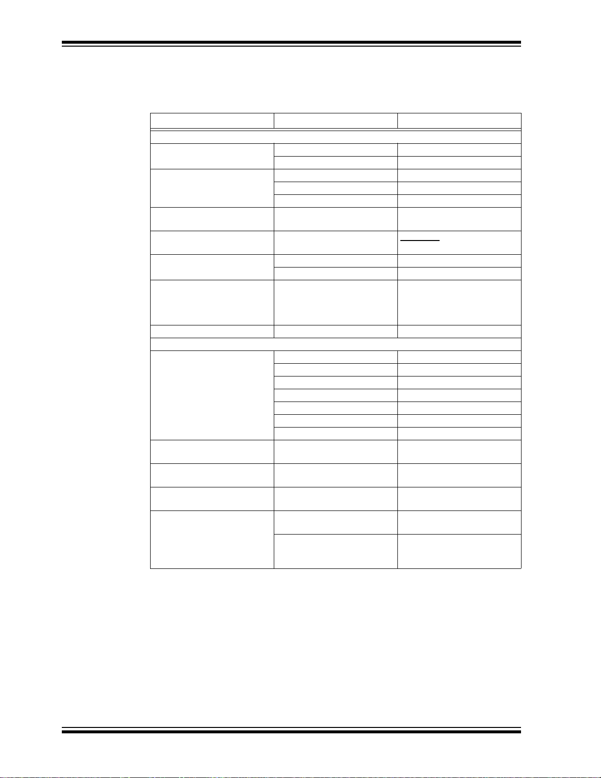
block. Figure 1-1 illustrates the LIN Serial Analyser tool connected to a network.
®
Windows®
© 2008 Microchip Technology Inc. DS51675B-page 5
Page 10
LIN Serial Analyzer User’s Guide Rev2.0
FIGURE 1-1: LIN SERIAL ANALYSER DEVELOPMENT TOOL
Optional
Power
Supply
Board Under Test
1.5 LIN SERIAL ANALYSER HARDWARE
The LIN Serial Analyser connects to a Microsoft® Windows® operating system
compatible computer using a USB port. It interfaces to the target network using a
three-position, screw-type terminal block.
FIGURE 1-2: LIN SERIAL ANALYSER
Status LEDs
LIN Tool
PC
USB Port
1.5.1 Status LEDs
The Status LEDs indicate the status of the LIN Serial Analyser. An illuminated LED
means:
• USB (green) – Power has been applied to the LIN Serial Analyser by the USB
port.
• Busy (yellow) – The LIN Serial Analyser is communicating with the LIN network.
• LIN (blue) – The LIN Serial Analyser is connected to the target bus.
DS51675B-page 6 © 2008 Microchip Technology Inc.
Page 11
LIN Serial Analyser Overview
1.5.2 USB Port Connection
The USB port connection is a USB mini-B connector. Connect the LIN Serial Analyser
to the PC using the cable supplied with the device.
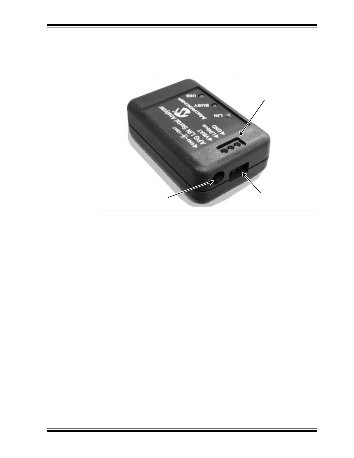
FIGURE 1-3: LIN SERIAL ANALYSER NETWORK AND POWER
Terminal
Block
Screws
Auxiliary
Power
1.5.3 Network Communication Connector
The communication connector connects to the target device using a three-position,
screw clamp terminal block. The pin assignments, labeled on the top of the device, are:
• VBAT – Positive battery connection for voltage supplied by the vehicle
• LIN – Bidirectional data I/O
• GND – Common chassis, power and serial ground
1.5.4 Power Jack
The device us es a stan dard, 6.5 x 2.5 DC pow er plug. Th e center pi n is posit ive. Powe r
can be supplied either through the power plug or the network connector as the two are
internally connected.
1.6 LIN SERIAL ANALYSER SOFTWARE
1.6.1 User Interface Program
The LIN Serial Analyser PC program displays all of the board’s bus activity via the
software’s Transaction window, displayed on the connected PC. This is useful for
“sniffing” the bus and tracking message frames.
Chapter 3. “LIN Serial Analyser PC Program” explains the installation and operation
of the program.
Network
Connection
1.6.2 Firmware
The LIN Serial Analyser firmware is explained in Chapter 9. “PICkit™ Serial Analyzer
Firmware” of the “PICkit™ Serial Analyzer User’s Guide” (DS51647).
© 2008 Microchip Technology Inc. DS51675B-page 7
Page 12

LIN Serial Analyzer User’s Guide Rev2.0
1.6.3 Dynamically Linked Library (DLL)
The LIN Serial Analyser DLL is explained in Chapter 10. “PICkit™ Serial Analyzer
DLL” of the “PICki t™ Serial An alyzer User’s Guide” (DS51647).
DS51675B-page 8 © 2008 Microchip Technology Inc.
Page 13

LIN SERIAL ANALYZER
USER ’S GUIDE REV2.0
Chapter 2. Getting Started – Quick Setup
2.1 HIGHLIGHTS
This chapter discusses:
• Using the LIN Serial Analyzer for the First Time
• Software Installation
• Running LIN Serial Analyser Program
2.2 USING THE LIN SERIAL ANALYZER FOR THE FIRST TIME
The LIN Serial Analyser is shipped preprogrammed and ready for use. The user needs
to supply:
• A wiring harness with appropriate connections to its system network
• A power supply (nominal 13.8V)
Before making any connections, the software must be installed on the host system. The
user must have administrator level rights to install some of the required programs. For
more information, see Section 2.3 “Software Installation”.
Power is supplied either through the round, power plug or the terminal block. The
positive and negative terminals and power plug are common. Supplied power must be
in the range of 8.0V to 30.0V with a nominal value of 12.0-14.4V. Less than 5.0 mA of
current is required to power the LIN transceiver section of the unit.
Internal jumper, E1, configures the unit as either a master or slave node. A 1.0 kΩ bus
pull-up resistor is enabled when E1 is connected across A and B. With the jumper
removed, an internal 30 kΩ resistor is retained.
The unit is configured as a master node as shipped.
2.3 SOFTWARE INSTALLATION
All necessary files are contained on the Compact Disc (CD) supplied with the device.
2.3.1 Installing the LIN Serial Analys er Program
1. Run setup.exe from the CD.
2. Select Install when prompted and follow any instructions.
Note: The LIN Serial Analyser program requires the Microsoft
version 2.0.
The PC host program is uninstalled with the control panel’s add/remove utility.
®
.NET Framework
2.4 RUNNING LIN SERIAL ANALYSER PROGRAM
Before starting the LIN Serial Analyser software:
• The analyzer must be connected to the PC by a USB cable
• The analyzer must be powered up
The analyzer’s green USB and blue LIN lights will be on when these conditions are
met.
© 2008 Microchip Technology Inc. DS51675B-page 9
Page 14

LIN Serial Analyzer User’s Guide Rev2.0
There is a hard-wired, loopback bus path, so connection to a network is not needed for
testing the installation.
To start the software:
1. On the Windows operating system taskbar, click Start.
2. Click All Programs>Microchip Technology Inc.>
3. Click Setup>COM port
4. From the pull-down menu, select the USB port to be used.
Note: Only available, plugged in USB ports are displayed by the pull-down menu.
If the correct serial port is not displayed, verify that the USB hardware is
correctly installe d.
5. In the menu’s text box, type the appropriate baud rate value.
6. Click OK.
7. Verify operation by selecting one of the preset messages from the Master
Message area.
Bus activity is indicated by the analyzer’s yellow BUSY light flickering.
A message will be displayed in the Bus Transaction window with:
•A time-stamp
• The correct ID parity bits
• The calculated checksum
• Any detected error conditions
.
LIN Serial Analyser.
DS51675B-page 10 © 2008 Microchip Technology Inc.
Page 15

Chapter 3. LIN Serial Analyser PC Program
3.1 HIGHLIGHTS
This chapter discusses:
• Interface Overview
• Transaction Window
• File Functions
• Setup Functions
• Tools Functions
• Start/Stop Logging Button
• Master Message Group Box
•Status Bar
3.2 INTERFACE OVERVIEW
When the LIN Serial Analyser’s software program starts, the window, shown in Figure ,
appears. The commands are accessed through the pull-down menus at the top of the
interface.LIN Serial Analyzer User Interface
LIN SERIAL ANALYZER
USER ’S GUIDE REV2.0
Pull-Down
Menus
Start/Stop
Logging
Button
Transaction
Window
Master
Message
Group Box
Status B ar
© 2008 Microchip Technology Inc. DS51675B-page 11
Page 16

LIN Serial Analyzer User’s Guide Rev2.0
3.3 T RANSACTION WINDOW
This window, shown in Figure 3-1, constantly monitors and display bus traffic when in
the “Display All” mode. Any message frames seen on the bus are shown, regardless of
the source.
The data is displayed as it is seen on the bus without modification.
This section describes the window’s fields.
FIGURE 3-1: MESSAGE FRAMES DISPLAY
3.3.1 TimeStamp
This field of the Transaction window displays the time, in seconds, since the last frame
was received. The value is reset to zero when the window is cleared.
The value can also be cleared by clicking on the “TimeStamp” column label.
3.3.2 ID (Identifier)
This field displays the ID byte, including the upper two parity bits.
3.3.3 Data
From zero to eight data bytes are displayed in this field. The data is in the hexadecimal
format (without the leading characters, ‘0x’), with the bytes separated by spaces.
3.3.4 Checksum
The last field of a frame is the checksum. The checksum contains the inverted, eight-bit
sum with carry, over all data bytes or all data bytes and the protected identifier.
3.3.5 ChkSumType
This field indicates whether a “classic” or “enhanced” equation was used for the checksum calculation. For messages sent via the Master Message group box, the type of
calculation is configured in the checksum portion of the Master Message group box
(see Section 3.8.3 “Checksum Group”).
• Classic – Checksum calculation over the data bytes only. Used for the master
request frame, slave response frame and communications with LIN 1.x slaves.
An eight-bit sum with carry is equivalent to the sum of all values and subtracts
255 every time the sum is greater than or equal to 256.
• Enhanced – Checksum calculation over the data bytes and the protected identifier
byte. Used for communication with LIN 2.x slaves.
The checksum is calculated both ways when a message frame is received. A match is
displayed either as “Classic” or “Enhanced”. If neither result matches the incoming
data, “ERROR” is displayed.
3.3.6 Baud
This field shows the actual, calculated bit rate observed during the Auto-Baud Detect
period of the current frame.
DS51675B-page 12 © 2008 Microchip Technology Inc.
Page 17

LIN Serial Analyser PC Program
3.3.7 Errors
This field displays any of the error types described in this section. If multiple errors are
detected, only one is displayed .
3.3.7.1 PARITY The parity is calculated on the frame identifier bits as shown in Equation 3-1.
EQUATION 3-1: PARITY CALCULATIONS
P0 = ID0 ℘? ID1 ℘? ID2 ℘?
P1 = - (ID1 ℘? ID3 ℘? ID4 ℘? I
† P0 is bit 6 and P1 is bit 7 of the ID byte.
3.3.7.2 TX BIT A slave or master node that is transmitting a bit on the bus also monitors the bus. A TX
bit error is when the bit or byte value that is received is different from the bit or byte
value that is transmitted.
Note: This function is not currently implemented.
3.3.7.3 CHECKSUM A checksum error is when the inverted modulo-256 sum over all received data bytes
and the protected identifier (when using enhanced checksum) and the received
checksum byte field does not result in $FF.
3.3.7.4 FRAMING A byte field framing error is when the ninth bit after a valid Start bit is dominant. This
check does not apply to the Break character.
Note: This function is not currently implemented.
†
3.3.7.5 NO ANSWER This value displays when a new Break/Sync/ID header was detected, but no data was
received within the bus time-out period.
3.3.7.6 BREAK This displays when data characters were received before a valid Sync Break header
was detected.
Note: This function is not currently implemented.
3.3.7.7 BUS TIME-OUT This value indicates that the time interval allocated for an eight-byte message expired.
This time is set to approximately 140% of a single bit time.
The time-out may also be configured to a fixed value not dependent on baud rate.
3.3.7.8 SWBREAK This value displays when a valid Sync Break is not detected by the UART . A Break was
“assumed” because the first byte received was 0x00, but without a framing error.
Note: This function is not currently implemented.
© 2008 Microchip Technology Inc. DS51675B-page 13
Page 18

LIN Serial Analyzer User’s Guide Rev2.0
3.4 FILE FUNCTIONS
3.4.1 Open
The “Open” dialog box loads configuration and master message frames from a
user-selected file into the “Master Frames” field, so that they can be sent (see
Section 3.8.1 “Master Frames Field”).
By default, the dialog box, shown in Figure 3-2, displays the file that was last used in
the previous session.
T o display the dialog box, go to the pull-down menus at the top of the user interface and
select File>Open
FIGURE 3-2: FILE OPEN WINDOW
.
3.4.2 Save
The “Save” dialog box saves configuration and master message frames, displayed
in the “Master Frames” field, to a previously selected *.ini file (see
Section 3.8.1 “Master Frames Field”.) By default, the dialog box populates the
file name that was last used in the previous session.
T o display the dialog box, go to the pull-down menus at the top of the user interface and
select File>Save
DS51675B-page 14 © 2008 Microchip Technology Inc.
.
Page 19

LIN Serial Analyser PC Program
3.4.3 Save As
The “Save As” dialog box saves or appends configuration and master message
frames, displayed in the “Master Frames” field, to a preselected file (see
Section 3.8.1 “Master Frames Field”). The default file name is the last used file from
the previous session.
To display the dialog box, shown in Figure 3-3, go to the pull-down menus at the top of
the user interface and select File>Save As
FIGURE 3-3: FILE “Save As” WINDOW
.
3.4.4 Print, Print Setup, Print Preview
These three functions relate to printing the contents of the Transaction window.
Print Setup
will appear.
The printing function clears the contents of the Transaction window, but does not reset
the time-stamp.
All of these functions are accessible through the File
configures the printing attributes and Print Preview displays how the print
pull-down menu.
3.4.5 Exit
Selecting File>Exit terminates the LIN Serial Analyser software program.
© 2008 Microchip Technology Inc. DS51675B-page 15
Page 20

LIN Serial Analyzer User’s Guide Rev2.0
3.5 SETUP FUNCTIONS
The Tools pull-down menu has the following commands.
3.5.1 Setup COM port
The “Setup COM port” function selects the USB communication port to use.
Note: The “COM port” drop-down list box displays only available, plugged-in USB
ports. If the correct serial port is not displayed in the menu, verify that the
USB hardware is correctly installed.
The menu also sets the baud rate to apply to master transactions.
The “Timeout in mS” text box displays the current time-out value for a message frame
and may be modified by the user. To enable the time-out value to vary with the baud
rate, enter a value of 0.
FIGURE 3-4: “Setup COM port” WINDOW
To display the dialog box, select Setup>COM port
.
DS51675B-page 16 © 2008 Microchip Technology Inc.
Page 21

LIN Serial Analyser PC Program
3.5.2 Log File
The Log File setup function specifies the new or existing file that will store bus
transactions.
If an existing file that already contains data is selected, any new messages will be
appended to the end of the file.
FIGURE 3-5: LOG FILE SETUP WINDOW
To display the dialog box, select Setup>Log File
.
© 2008 Microchip Technology Inc. DS51675B-page 17
Page 22

LIN Serial Analyzer User’s Guide Rev2.0
3.5.3 Slave Response
The Slave Response setup function specifies message frames that are published to the
bus whenever the correct ID is recognized.
FIGURE 3-6: SLAVE RESPONSE SETUP WINDOW
To display the dialog box, select Setup>Slav e Response
.
3.5.4 Slave Response Frames Field
The “Slave Response Frames” field is composed of 0 to n rows of one or more messages that are sent over the bus in response to a valid ID byte. These messages can
be entered manually, loaded from a previously saved session, or both.
When the response is sent, it is displayed in the Transaction window if it is open and
active.
Messages in the “Slave Response Frames” field can also be saved for reuse (see
Section 3.4.2 “Save” and Section 3.4.3 “Save As”).
3.5.4.1 RESPONSE SYNTAX
Messages must consist of the ID byte without parity bits and the data bytes, all
separated by spaces. All inputs are in hexadecimal radix.
The checksum is not included; it is calculated at send time unless the “forced” Checksum option is selected.
Comments or notes may be attached to each frame by prefacing it with a
semi-colon (;). Any text after the semi-colon will be disregarded and not transmitted. All
notes will be saved in the selected .ini file and reloaded when reopened.
DS51675B-page 18 © 2008 Microchip Technology Inc.
Page 23

LIN Serial Analyser PC Program
3.5.4.2 DEVELOPING AND STORING RESPONSE CONTENT To manually add a slave response message content to the “Slave Response Frames”
field:
1. Click the Add button. A second window displays for creation of the new message.
2. Type the message in the text box.
3. Click OK.
To load a pre-existing message to the “Slave Response Frames” field:
WARNING
Importing a file into the “Slave Response Fram es” fi eld ov er writes any content that previously had been in that field.
1. From the pull-down menus, select File>Open
2. In the dialog box’s list box, select the desired *.ini file.
3. Click Open.
To delete some slave message content:
1. In the “Slave Response Frames” field, select the content to be deleted by doing
one of the following:
•To select adjacent rows of cont ent – Click on the first row, scroll down to the
last row and hold down <Shift> while clicking.
•To select non-adjacent rows of content – Hold down <Ctrl> while clicking each
row.
2. Click Delete.
To edit some slave message content:
1. In the “Master Frames” field, select the content line to be edited
1. Click Edit. A second window displays to edit hte message.
2. Make and corrections or additions to the message in the text box.
3. Click OK
To store a slave response message(s) into the buffer:
1. In the “Slave Responser Frames” field, select the content to be stored by doing
one of the following:
•To select adjacent rows of cont ent – Click on the first row, scroll down to the
last row and hold down <Shift> while clicking.
•To select non-adjacent rows of content – Hold down <Ctrl> while clicking each
row.
2. Click Save.
The highlighted message content is stored, working top-to-bottom through the
“Slave Response Frames” field.
The internal buffer status is updated to reflect the amount a bytes used and
remaining. If the amount of buffer space is exceeded, the Save operation is
aborted and a error message displayed. Reduce the number or size of the messages to be written to the buffer and retry the Save.
. The “Open” dialog box appears.
© 2008 Microchip Technology Inc. DS51675B-page 19
Page 24

LIN Serial Analyzer User’s Guide Rev2.0
To save a slave reponse message to a file:
1. See Section 3.4.2 “Save” and Section 3.4.3 “Save As”.
3.5.4.3 SLAVE RESPON S E FR AMES FIELD ELEMENTS This section describes the “Slave Response Frames ” field’s two elements.
3.5.4.3.1 ID
The “ID” element displays the identifier byte that is compared to identifier bytes
received from the bus. The ID is entered without the upper two parity bits. Parity is calculated and appended when the message frame is stored in the inernal buffer memory.
The acceptable range of values is 00 to 3F hex (0 to 63 decimal).
3.5.4.3.2 DATA
The “Data” portion of the “Slave Response Frames” field displays zero to eight-byte val-
ues, separated by spaces. This are the actual bytes sent over the bus in response to a
recognized ID.
3.5.5 Slave Response Message Controls
3.5.5.1 SAVE BUTTON Clicking this button stores the selected message content highlighted in the “Slave
Response Frames” field (see the “Save” procedure in Section 3.5.4.2 “Developing
and Storing Response Content”).
3.5.5.2 ADD BUTTON Click the Add button to add a new message to the “Slave Response” field
3.5.5.3 EDIT BUTTON Allows the selected message in the “Slave Response Frames” field to be edited.
3.5.5.4 DELETE BUTTON Clicking the Delete button deletes the content that is highlighted in the “Master Frames”
field. (see the “Delete” procedure in Section 3.5.4.2 “Developing and Storing
Response Content”).
3.5.5.5 CLEAR ALL BUTTON Clicking this button clears the both the contents of the “Slave Response Frames” win-
dow and the internal buffer memory. The buffer status is updated to show no used bytes
and bytes remaining.
3.5.6 Checksum Group
The checksum value is computed at send time. Selecting one of the
option buttons in the “Checksum” group, shown at right, determines
the type of checksum that will be calculated for all transmitted
master message frames, highlighted in the “Master Frames” field.
• classic – The checksum includes all data bytes.
• enhanced – The checksum includes identifier byte and all data
bytes.
• forced – (Enabled only in Debug mode.) The last byte in the message string is
sent in place of the calculated checksum. This is useful in checking master error
handling.
DS51675B-page 20 © 2008 Microchip Technology Inc.
Page 25

LIN Serial Analyser PC Program
The checksum returned by the slave will be displayed in the “Checksum” field of the
Transaction window (see Section 3.3.5 “ChkSumType”.)
© 2008 Microchip Technology Inc. DS51675B-page 21
Page 26

LIN Serial Analyzer User’s Guide Rev2.0
3.6 TOOLS FUNCTIONS
This sections lists the commands on the Tools pull-down menu.
3.6.1 Debug Mode
Selecting Tools>Debug Mode enables the user to debug bus or slave operational
issues.
One function forces a user-supplied checksum to be appended to a master message
to check a slave for proper error handling. In this mode, the generation of identifier
parity bits is inhibited and the identifier byte is transmitted without modification.
3.6.2 Suppress Bus Time-out Error
The current implementation of the master task cannot refer to a LIN descriptor file, so
there is no way to determine the length of any received message. To calculate an
appropriate time-out value, multiply the length of an eight-byte frame times 140% of the
bit rate.
This value can be overridden by entering a fixed time-out value in the COM Setup
window, described in Section 3.5.1 “Setup COM port”.
3.6.3 Clear Monitor Window
This function clears the Transaction window and resets the time-stamp.
3.6.4 Filters
This opens a window to display all messages received through the Transaction window
but are sorted by ID number. The window is ‘live’ and shows current bus traffic. New
message frames received will overwrite previous data. This is useful in monitoring constanly changes data.
3.6.5 Transmit
This option selects the Transmit Only mode. No received messages are displayed in
the Transaction window.
3.6.6 Listen (Filter)
This option selects the Listen Only mode. Only non-duplicated messages are displayed
in the Transaction window.
When “snooping” bus message frames, this prevents the Transaction window from
becoming cluttered with repeated frames.
3.6.7 Display All (Snoop) Default
This function selects the Display All mode. All messages seen on the bus are
displayed.
This mode is best used with the data logging feature to capture all bus traffic for later
analysis.
DS51675B-page 22 © 2008 Microchip Technology Inc.
Page 27

LIN Serial Analyser PC Program
e
3.7 START/STOP LOGGING BUTTON
This button – located in the top, right corner of the interface – starts, pauses, or stops
the capturing of messages to the log file.
Before starting the logging process, select and open a log file (see Section 3.5.2 “Log
File”).
To pause the logging process, click the button a second time.
3.8 MASTER MESSAGE GROUP BOX
This functions in the group box to act as a master node on the LIN bus, sending the
previously constructed frames to the slaves on the bus.
This window will cause a bus conflict if another master appears on the network. Any
conflict will be shown in an active Transaction window as a bus error.
The group box, shown in Figure 3-7, consists of the:
• “Master Frames” field
• “Checksum” group
• Message controls
FIGURE 3-7: MASTER MESSAGE GROUP BOX
“Master Fram
Field
“Checksu
Group
Message
Controls
3.8.1 Master Frames Field
The “Master Frames” field is composed of 0 to n rows of one or more messages that
can be sent over the bus for test purposes. These messages can be entered manually,
loaded from a previously saved session, or both.
When the message is sent, it and any response is displayed in the Transaction window
if it is open and active.
Messages in the “Master Frames” field can also be saved for reuse (see
Section 3.4.2 “Save” and Section 3.4.3 “Save As”).
3.8.1.1 MESSAGE SYNTAX Messages must consist of the ID byte without parity bits and the data bytes, all
separated by spaces. All inputs are in hexadecimal radix.
The checksum is not included; it is calculated at send time.
Comments or notes may be attached to each frame by prefacing it with a
semi-colon (;). Any text after the semi-colon will be disregarded and not transmitted. All
notes will be saved in the selected .ini file and reloaded when reopened.
© 2008 Microchip Technology Inc. DS51675B-page 23
Page 28

LIN Serial Analyzer User’s Guide Rev2.0
3.8.1.2 DEVELOPING AND STORING MESSAGE CONTENT
To manually add message content to the “Master Frames” field:
1. Click the Add button. A second window displays for creation of the new mes-
sage.
2. Type the message in the text box.
3. Click OK.
To load a pre-existing message to the “Master Frames” field:
WARNING
Importing a file into the “Master Frames” field overwrites any content that previously
had been in that field.
1. From the pull-down menus, select File>Open
2. In the dialog box’s list box, select the desired *.ini file.
3. Click Open.
To delete some message content:
1. In the “Master Frames” field, select the content to be deleted by doing one of the
following:
•To select adjacent rows of cont ent – Click on the first row, scroll down to the
last row and hold down <Shift> while clicking.
•To select non-adjacent rows of content – Hold down <Ctrl> while clicking each
row.
2. Click Delete.
To edit some message content:
1. In the “Master Frames” field, select the content line to be edited
1. Click Edit. A second window displays to edit hte message.
2. Make and corrections or additions to the message in the text box.
3. Click OK
To send a message:
1. In the “Master Frames” field, select the content to be sent by doing one of the
following:
•To select adjacent rows of cont ent – Click on the first row, scroll down to the
last row and hold down <Shift> while clicking.
•To select non-adjacent rows of content – Hold down <Ctrl> while clicking each
row.
2. Click Send.
The highlighted message content is sent, working top-to-bottom through the
“Master Frames” field.
The message is sent once. (For information on continuall y se ndi ng the
highlighted message content, see Section 3.8.3 “Checksum Group”.)
. The “Open” dialog box appears.
DS51675B-page 24 © 2008 Microchip Technology Inc.
Page 29

LIN Serial Analyser PC Program
To store a message:
1. See Section 3.4.2 “Save” and Section 3.4.3 “Save As”.
3.8.1.3 MASTER FRAMES FIELD ELEMENTS This section describes the “Master Frames” field’s two elements.
3.8.1.3.1 ID
The “ID” element displays the identifier byte to be sent without the upper two parity bits.
Parity is calculated and appended at send time unless the application is in the Debug
mode (see Section 3.6.1 “Debug Mode”).
The acceptable range of values is 00 to 3F hex (0 to 63 decimal).
3.8.1.3.2 DATA
The “Data” portion of the “Master Frames” field displays zero to eight-byte values,
separated by spaces.
3.8.2 Message Controls
3.8.2.1 SEND BUTTON Clicking this button transmits the message content that is highlighted in the “Master
Frames” field (see the “Send” procedure in Section 3.8.1.2 “Developing and Storing
Message Content”).
When the Send button is clicked, the message is sent once (see
Section 3.8.3 “Checksum Group”).
If the Transaction window is open and active, the message and any response will be
displayed.
3.8.2.2 CONTINUOUS BUTTON Clicking the Continuous button sends the selected message entry or entries continu-
ously, at an interval defined in the time control text box, described next. A second click
of the button stops the continuous transmissions.
Any number of messages may be selected for continuous broadcast. They will be
transmitted in the order they appear in the “Master Frames” field.
3.8.2.3 TIME CONTROL Used in conj unction with the Continuous button, this text box sets the interval, in
milliseconds, between message frames being sent in the Continuous mode.
Note: Due to service latency time in the Windows operating system environment,
the minimum time interval may be as high as 200 ms, regardless of desired
time set in the control box. Intervals less than 200 ms will be serviced as
fast as possible, but may not be less than the operating system minimum.
3.8.2.4 ADD BUTTON Click the Add button to add a new message to the “Master Frames” field
3.8.2.5 EDIT BUTTON Allows the selected message in the “Master Frames” field to be edited.
© 2008 Microchip Technology Inc. DS51675B-page 25
Page 30

LIN Serial Analyzer User’s Guide Rev2.0
3.8.2.6 DELETE BUTTON
Clicking the Delete button deletes the content that is highlighted in the “Master Frames”
field. (see the “Delete” procedure in Section 3.8.1.2 “Developing and Storing Message
Content”).
3.8.3 Checksum Group
The checksum value is computed at send time. Selecting one of the
option buttons in the “Checksum” group, shown at right, determines
the type of checksum that will be calculated for all transmitted
master message frames, highlighted in the “Master Frames” field.
• classic – The checksum includes all data bytes.
• enhanced – The checksum includes identifier byte and all data
bytes.
• forced – (Enabled only in Debug mode.) The last byte in the message string is
sent in place of the calculated checksum. This is useful in checking slave error
handling.
If a slave response is requested (a ID value with no data bytes), the checksum is not
computed and the field is left blank.
The checksum returned by the slave will be displayed in the “Checksum” field of the
Transaction window (see Section 3.3.5 “ChkSumType”.)
3.9 STATUS BAR
The status bar at the bottom of the Interface window displays:
• Currently selected baud rate of master messages
• Dynamic LIN network status
DS51675B-page 26 © 2008 Microchip Technology Inc.
Page 31

LIN SERIAL ANALYZER
USER ’S GUIDE REV2.0
Appendix A. LIN Serial Analyzer Technical Information
A.1 HIGHLIGHTS
This chapter discusses:
• LIN Serial Analyzer Schemati c
A.2 LIN SERIAL ANALYZER SCHEMATIC
The LIN Serial Analyzer management hardware diagram is shown in Figure A-1.
© 2008 Microchip Technology Inc. DS51675B-page 27
Page 32

LIN Serial Analyzer User’s Guide Rev2.0
FIGURE A-1: LIN SERIAL ANALYZER SCHEMATIC
P2
BUS
V
D-2D+3nc4GND
1
5
USB Mini-B
R14.7KLED1 Blue LED
R2470
LED2 Yellow LED
DD
V
R7
R5
C4
C3
3
R4470
CC
V
LED3 Green LED
R6 0
100K
100K
.01 MF
1.0 MF
V
DD
C10
CC
V
0.1 MF
D5
C9
470 nF
RX
TX
CSWAKE
FAULT/TXE
1N4004
BUSY
20
18
19
RB0/INT0/AN12
RB1/INT1/AN10
25
22
24
23
21
RB6KBI2/PGC
RB3/AN9/VPO
RB7/KBI3/PGD
RB5/KBI1/PGM
RB4/AN11/KBI0
RB2/AN8/INT2/VMO
CC
V
V
DD
17
4
2
8
TX
1
RX
U2
/RE3
PP
11
13
10
9
12
14
USB
V
RC4/D-/VM
RC5/D+/VP
15
RC6/TX/CK
RC7/RX/DT
8
RC2/CCP1
RC1/T1OSI/UOE
RC0/T1OSO/T13CKI
-
+
REF
REF
GND
GND
16
5
CC
V
R104.7K
PIC18F2450-QFN
RA3/AN3/V
RA4/T0CLI/RCV
RA5/AN4/LVDIN
3
4
2
USB_ATTACH
R9 100K
D3
1N4148WX-TP
BB
V
D2 1N4004
BAT
GND
LBUS
V
123
J1
C2
C1
D1
U1
.01 MF
10 MF
7
CS/WAKE
V
BAT
FAULT/TXE
LIN
6
R3 1K
E1
C5
D4
1 2
P6SMB43AT3G
GND
MCP2021-500
5
220 pF
MMBZ27VCLT1G
231
LIN_ATTACH
P1
26
J2
MCLR/V
OSC1/CLKIN
6
C6 22 pF
CC
V
12345
TM
PICkit 2
OSC2/CLKOUT/RA6
7
20 MHz
Y1
C8 22 pF
0.1 MF
C7
6
RA0/AN0
RA1/AN1
1
27
28
R810K
RA2/AN2/V
DS51675B-page 28 © 2008 Microchip Technology Inc.
Page 33

Index
LIN SERIAL ANALYZER
USER ’S GUIDE REV2.0
B
Buttons
Start/Stop Logging............................................19
C
Clear Monitor Window Function...............................18
Customer Support......................................................3
D
Data Field Element .................................................. 21
Debug Mode Function..............................................18
Display All (Snoop) Default Function.......................18
Documentation
Additional Reading........................... ...... ..... ...... ..3
Conventions........................................................2
Layout................................................................. 1
E
Exit Function.......................... ...... ...... ..... ...... ........... 15
F
File Menu
Exit....................................................................15
Open................................................................. 14
Print .................................................................. 15
Save..................................................................14
Save As ............................................................ 15
H
Hardware
Connecting to PC.............................................. ..6
Contents of Kit................................. ...... ............. 5
LIN Serial Analyzer Schematic.........................24
Network Connector............................................. 7
Overview ............................................................. 5
Power Jack.........................................................7
Status LEDs........................................................6
USB Connection.................................................7
I
ID Field Element ......................................................20
Installing Software......................................................9
Internet Address.........................................................3
L
LIN Serial Analyzer User Interface........................... 11
Listen (Filter) Function............................ .................18
Log File Function.....................................................17
M
Master Frames Field
Data ..................................................................21
Deleting Message Content..................... ...........20
Developing and Storing
Message Content...............................20
ID ......................................................................20
Loading Pre-Existing Message Content............20
Manually Creating a Message ..........................20
Saving Message Content..................................20
Sending Messages...........................................20
Master Message Group Box....................................19
Checksum Group..............................................22
Master Frames Field.........................................19
Master Frames Field Elements.........................20
Message Controls.............................................21
Message Controls
Continuous Button............................................21
Delete Button....................................................21
Send Button......................................................21
Time Control .....................................................21
Messages
Creating Manually.............................................20
Deleting Message Content..................... ...........20
Developing and Storing.......................... ...........20
Loading Pre-Existing Content...........................20
Saving Message Content..................................20
Sending.............................................................20
Microchip Internet Web Site.......................................3
O
Open Function..........................................................14
P
Print Function...........................................................15
Print Preview Function.............................................15
Print Setup Function.................................................15
S
Save As Function............................................... ......15
Save Function................... ..... ...... ...... ..... .................14
Setup COM port Function........................................16
Setup Menu..............................................................16
Log File.............................................................17
Setup COM port................................................16
© 2008 Microchip Technology Inc. DS51675B-page 25
Page 34

LIN Serial Analyzer User’s Guide Rev2.0
Software
Dynamically Linked Library (DLL).......................8
File Menu..........................................................14
Firmware.............................................................8
Installation...........................................................9
Interface Window..............................................11
Master Message Group Box .............................19
Overview.............................................................8
Prelaunch Tasks.................................................9
Setup Menu.......................................................16
Starting the Software ........................................10
Status Bar.........................................................22
Tools Menu.......................................................18
Transaction Window.........................................12
Start/Stop Logging Button........................................19
Suppress ‘Bus Timeout’ Error Function..... ..... ...... ....18
T
Tools Menu ..............................................................18
Clear Monitor Window.......................................18
Debug Mode .....................................................18
Display All Default.............................................18
Listen (Filter).....................................................18
Suppress ‘Bus Timeout’ Error...........................18
Transmit............................................................18
Transaction Window.................................................12
Baud..................................................................12
Checksum.........................................................12
ChkSumType ....................................................12
Data...................................................................12
Errors ................................................................13
Break..........................................................13
Bus Time-out..............................................13
Checksum..................................................13
Framing......................................................13
No Answer .................................................13
Parity..........................................................13
SWBreak....................................................13
TX Bit.............................. ...... ...... ..... ...... ....13
ID (Identifier) .....................................................12
TimeStamp........................................................ 12
Transmit Function.....................................................18
W
WWW Address...........................................................3
DS51675B-page 26 © 2008 Microchip Technology Inc.
Page 35

NOTES:
Index
© 2008 Microchip Technology Inc. DS51675B-page 27
Page 36

WORLDWIDE SALES AND SERVICE
AMERICAS
Corporate Office
2355 West Chandler Blvd.
Chandler, AZ 85224-6199
Tel: 480-792-7200
Fax: 480-792-7277
Technical Support:
http://support.microchip.com
Web Address:
www.microchip.com
Atlanta
Duluth, GA
Tel: 678-957-9614
Fax: 678-957-1455
Boston
Westborough, MA
Tel: 774-760-0087
Fax: 774-760-0088
Chicago
Itasca, IL
Tel: 630-285-0071
Fax: 630-285-0075
Dallas
Addison, TX
Tel: 972-818-7423
Fax: 972-818-2924
Detroit
Farmington Hills, MI
Tel: 248-538-2250
Fax: 248-538-2260
Kokomo
Kokomo, IN
Tel: 765-864-8360
Fax: 765-864-8387
Los Angeles
Mission Viejo, CA
Tel: 949-462-9523
Fax: 949-462-9608
Santa Clara
Santa Clara, CA
Tel: 408-961-6444
Fax: 408-961-6445
Toronto
Mississauga, Ontario,
Canada
Tel: 905-673-0699
Fax: 905-673-6509
ASIA/PACIFIC
Asia Pacific Office
Suites 3707-14, 37th Floor
Tower 6, The Gateway
Harbour City, Kowloon
Hong Kong
Tel: 852-2401-1200
Fax: 852-2401-3431
Australia - Sydney
Tel: 61-2-9868-6733
Fax: 61-2-9868-6755
China - Beijing
Tel: 86-10-8528-2100
Fax: 86-10-8528-2104
China - Chengdu
Tel: 86-28-8665-5511
Fax: 86-28-8665-7889
China - Fuzhou
Tel: 86-591-8750-3506
Fax: 86-591-8750-3521
China - Hong Kong SAR
Tel: 852-2401-1200
Fax: 852-2401-3431
China - Qingdao
Tel: 86-532-8502-7355
Fax: 86-532-8502-7205
China - Shanghai
Tel: 86-21-5407-5533
Fax: 86-21-5407-5066
China - Shenyang
Tel: 86-24-2334-2829
Fax: 86-24-2334-2393
China - Shenzhen
Tel: 86-755-8203-2660
Fax: 86-755-8203-1760
China - Shunde
Tel: 86-757-2839-5507
Fax: 86-757-2839-5571
China - Wuhan
Tel: 86-27-5980-5300
Fax: 86-27-5980-5118
China - Xian
Tel: 86-29-8833-7252
Fax: 86-29-8833-7256
ASIA/PACIFIC
India - Bangalore
Tel: 91-80-4182-8400
Fax: 91-80-4182-8422
India - New Delhi
Tel: 91-11-4160-8631
Fax: 91-11-4160-8632
India - Pune
Tel: 91-20-2566-1512
Fax: 91-20-2566-1513
Japan - Yokohama
Tel: 81-45-471- 6166
Fax: 81-45-471-6122
Korea - Daegu
Tel: 82-53-744-4301
Fax: 82-53-744-4302
Korea - Seoul
Tel: 82-2-554-7200
Fax: 82-2-558-5932 or
82-2-558-5934
Malaysia - Penang
Tel: 60-4-646-8870
Fax: 60-4-646-5086
Philippines - Manila
Tel: 63-2-634-9065
Fax: 63-2-634-9069
Singapore
Tel: 65-6334-8870
Fax: 65-6334-8850
Taiwan - Hsin Chu
Tel: 886-3-572-9526
Fax: 886-3-572-6459
Taiwan - Kaohsiung
Tel: 886-7-536-4818
Fax: 886-7-536-4803
Taiwan - Taipei
Tel: 886-2-2500-6610
Fax: 886-2-2508-0102
Thailand - Bangkok
Tel: 66-2-694-1351
Fax: 66-2-694-1350
EUROPE
Austria - Wels
Tel: 43-7242-2244-39
Fax: 43-7242-2244-393
Denmark - Copenhagen
Tel: 45-4450-2828
Fax: 45-4485-2829
France - Paris
Tel: 33-1-69-53-63-20
Fax: 33-1-69-30-90-79
Germany - Munich
Tel: 49-89-627-144-0
Fax: 49-89-627-144-44
Italy - Milan
Tel: 39-0331-742611
Fax: 39-0331-466781
Netherlands - Drunen
Tel: 31-416-690399
Fax: 31-416-690340
Spain - Madrid
Tel: 34-91-708-08-90
Fax: 34-91-708-08-91
UK - Wokingham
Tel: 44-118-921-5869
Fax: 44-118-921-5820
06/25/07
DS51675B-page 32 © 2008 Microchip Technology Inc.
 Loading...