

Page 1
LG8271/LG9271
Low-Power Long Range (LoRa®) Technology Gateway
Module for US (LG9271) and EU (LG8271)
General Features
• Supports LoRa®/LoraWAN™ Technology RF
Packets
• Up to eight receive and one transmit channel(s)
• UART (TTL) interface with built-in control protocol
• Compact form factor 90.0 mm x 30.0 mm
• mPCIe physical connector
• Environmentally friendly RoHS compliant
• Compliance:
- LG8271: Certified to R&TTE RF Standards
- LG9271: Certified to FCC Modular Transmit-
ter Standards
• Device Firmware Upgrade (DFU) over UART, see
®
Technology Gateway Module Software
“LoRa
Specifications”
Operational
• Single operating voltage: 3.0V to 3.6V (3.3V
nominal)
• Temperature range: -40 to +85 °C
• Supports LoRa Technology (12.5 kbps) and FSK
(EU only) (up to 300 kbps) modulations
• Integrated frequency matched RF front end, RF
transceiver, baseband processor, and MCU
The multi-channel, flexible nature of these modules
makes them ideal for use in LoRa Technology gateway
applications.
The advanced command protocol available over the
UART interface provides complete control over the full
capabilities of RF subsystem in addition to packet
reception and transmission.
Applications
Applications deploying LoRa Technology where gateway devices are required include:
• Automated Meter Reading
• Home and Building Automation
• Wireless Alarm and Security Systems
• Industrial Monitoring and Control
• Machine to Machine (M2M)
• Internet of Things (IoT)
Description
Microchip's LG8271/LG9271 Low-Power Long Range
(LoRa) Technology transceiver modules provide an
easy to use, low-power solution for long range wireless
data reception. Each module provides eight LoRa
Technology receive channels (125 kHz Bandwith
(BW)). In addition to the eight LoRa Technology
receive channels, the modules provide two additional
receive channels. The first is a LoRa Technology modulation receive channel capable of 125, 250 or 500 kHz
BW). The second provides an FSK/GFSK (EU only)
receive channel.
Beyond its receiver capability, the modules provide a
single flexibly transmit channel. This transmit channel
is capable of both LoRa Technology and FSK/GFSK
modulations at multiple bandwidths (LoRa Technology)
or baud rates (FSK/GFSK).
2017 Microchip Technology Inc. Preliminary DS00000000A-page 1
Page 2

LG8271/LG9271
Table of Contents
Device Overview ................................................................................................................................................................................... 3
General Specifications .......................................................................................................................................................................... 7
Typical Hardware Connections ............................................................................................................................................................11
Application Information ........................................................................................................................................................................ 13
Regulatory Approval ............................................................................................................................................................................ 15
Appendix A: Revision History .............................................................................................................................................................. 19
The Microchip Web Site ...................................................................................................................................................................... 21
Customer Change Notification Service ............................................................................................................................................... 21
Customer Support ............................................................................................................................................................................... 21
Product Identification System .............................................................................................................................................................. 22
TO OUR VALUED CUSTOMERS
It is our intention to provide our valued customers with the best documentation possible to ensure successful use of your Microchip
products. To this end, we will continue to improve our publications to better suit your needs. Our publications will be refined and
enhanced as new volumes and updates are introduced.
If you have any questions or comments regarding this publication, please contact the Marketing Communications Department via
E-mail at docerrors@microchip.com. We welcome your feedback.
Most Current Data Sheet
To obtain the most up-to-date version of this data sheet, please register at our Worldwide Web site at:
http://www.microchip.com
You can determine the version of a data sheet by examining its literature number found on the bottom outside corner of any page.
The last character of the literature number is the version number, (e.g., DS30000000A is version A of document DS30000000).
Errata
An errata sheet, describing minor operational differences from the data sheet and recommended workarounds, may exist for current
devices. As device/documentation issues become known to us, we will publish an errata sheet. The errata will specify the revision
of silicon and revision of document to which it applies.
To determine if an errata sheet exists for a particular device, please check with one of the following:
• Microchip’s Worldwide Web site; http://www.microchip.com
• Your local Microchip sales office (see last page)
When contacting a sales office, please specify which device, revision of silicon and data sheet (include literature number) you are
using.
Customer Notification System
Register on our web site at www.microchip.com to receive the most current information on all of our products.
DS00000000A-page 2 Preliminary 2017 Microchip Technology Inc.
Page 3
LG8271/LG9271
1.0 DEVICE OVERVIEW
The LG8271/LG9271 transceiver modules feature
LoRa Technology RF modulation, which provides long
range spread spectrum communication with high
interference immunity.
Each module supports eight (8) receive channels
allowing it to receive up to eight LoRa Technology
modulated packets simultaneously. By using LoRa
Technology modulation technique, LG8271/LG9271
can achieve a receiver sensitivity of -146 dBm. When
combined with LoRa Technology transmission devices,
the LG8271/LG9271 can provide a system with
industry leading link budget, which makes it optimal for
applications requiring extended range and robustness.
The LG8271/LG9271 modules also contain an integrated output power amplifier (LNA) providing optimal
downlink signal levels.
FIGURE 1-2: PIN DIAGRAM
LoRa Technology modulation also provides significant
advantages in both blocking and selectivity compared
to the conventional modulation techniques, solving the
traditional design compromise between extended
range, interference immunity, and low-power
consumption.
The LG8271/LG9271 modules deliver exceptional RF
selectivity and their multi-channel performance make
them ideal for use in LoRa Technology gateway
applications.
Figure 1-1, Figure 1-2 and Figure 1-3 show the top and
bottom view, the pinout, and the block diagram of the
modules.
FIGURE 1-1: TOP VIEW
2017 Microchip Technology Inc. Preliminary DS00000000A-page 3
Page 4
LG8271/LG9271
PIC24FJ128GB204
LoRaBaseband
Semtech
SX1301
RFESX1257
RFESX1257
RF
Switch,
PA/
LNA
RFE,etc.
FIGURE 1-3: BLOCK DIAGRAM
Debug
SPI
I/Q
UART
24LC08B
EEPROM
Table 1-1 describes the pins of the module.
TABLE 1-1: PIN DESCRIPTION
Pin Symbol Type Description
1 NC — Not Connected
2 VDD Power Positive Supply Terminal
3 HOST_INT Output Interrupt to the Host CPU
4 GND Power Ground Supply Terminal
5 PPS Input GPS PPS Input signal
6 NC — Not Connected
7 NC — Not Connected
8 NC — Not Connected
9 GND Power Ground Supply Terminal
10 NC — Not Connected
11 NC — Not Connected
12 NC — Not Connected
13 NC — Not Connected
14 NC — Not Connected
15 GND Power Ground Supply Terminal
16 NC — Not Connected
17 HOST_URX Input Module UART Receive
18 GND Power Ground Supply Terminal
19 HOST_UTX Output Module UART Transmit
20 RF_ENABLE Input RF Enable Input
21 GND Power Ground Supply Terminal
22 RESET Input Reset Module
23 NC — Not Connected
24 VDD Power Positive Supply Terminal
25 NC — Not Connected
26 GND Power Ground Supply Terminal
27 GND Power Ground Supply Terminal
28 NC — Not Connected
I/Q
DS00000000A-page 4 Preliminary 2017 Microchip Technology Inc.
Page 5
TABLE 1-1: PIN DESCRIPTION (CONTINUED)
Pin Symbol Type Description
29 GND Power Ground Supply Terminal
30 HOST_CLK Input Host I
31 NC — Not Connected
32 HOS_SDA Input/Output HOST I
33 NC — Not Connected
34 GND Power Ground Supply Terminal
35 GND Power Ground Supply Terminal
36 USB_D- — Host USB D37 GND Power Ground Supply Terminal
38 USB_D+ — Host USB D+
39 VDD Power Positive Supply Terminal
40 GND Power Ground Supply Terminal
41 VDD Power Positive Supply Terminal
42 LED1 Output LED1 Output
43 GND Power Ground Supply Terminal
44 LED2 Output LED2 Output
45 HOST_MISO Ouput Module SPI Slave Output
46 LED3 Output LED3 Output
47 HOST_MISO Input Module SPI Slave Input
48 PIC_DETECT Input/Output PCI Bus Detect Input.
49 HOST_SS Input Module SPI Slave Select Input
50 GND Power Ground Supply Terminal
51 HOST_SCK Input Module SPI Clock Input
52 VDD Power Positive Supply Terminal
LG8271/LG9271
2
C Clock
2
C Data
Low = SPI Mode, High = mPCIe/UART
2017 Microchip Technology Inc. Preliminary DS00000000A-page 5
Page 6

LG8271/LG9271
NOTES:
DS00000000A-page 6 Preliminary 2017 Microchip Technology Inc.
Page 7
LG8271/LG9271
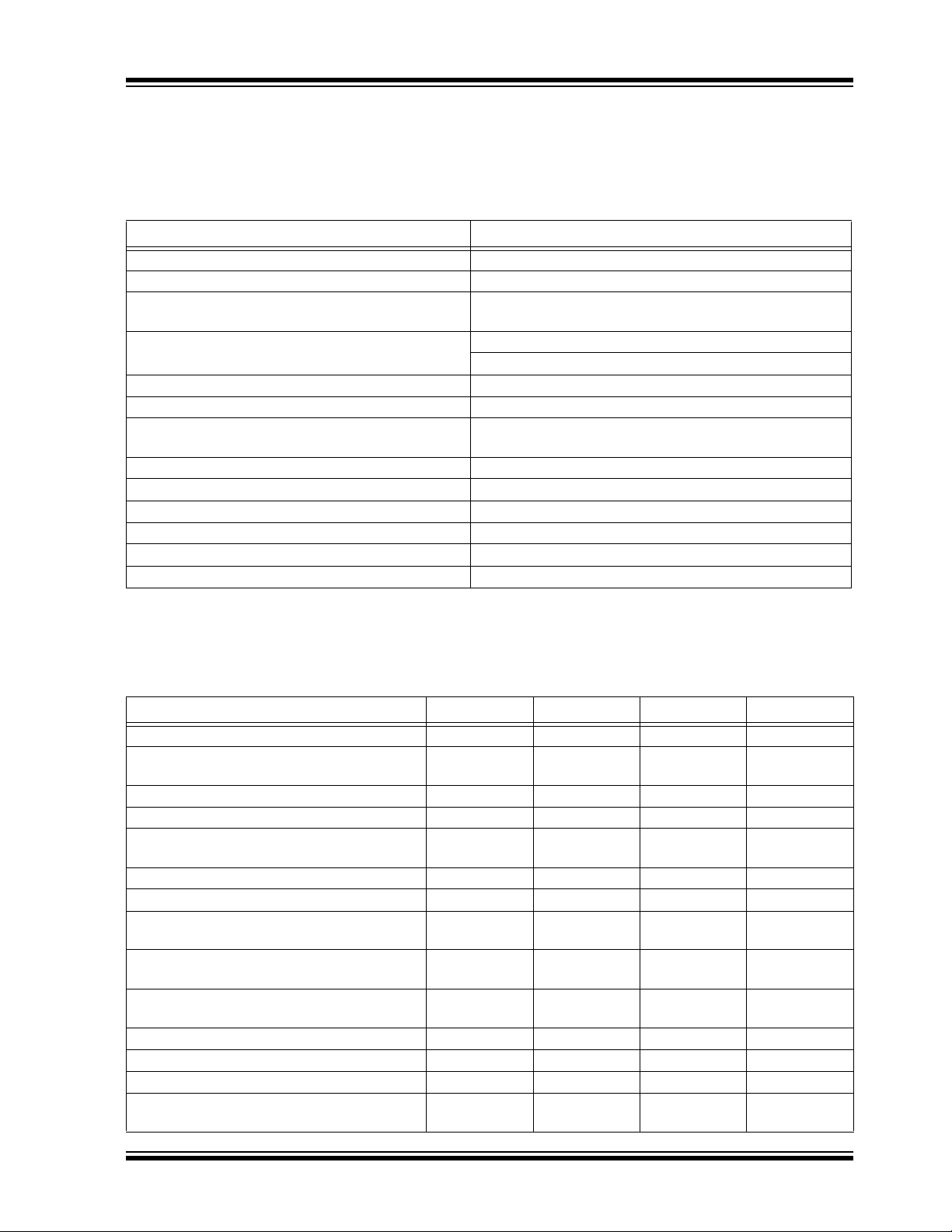
2.0 GENERAL SPECIFICATIONS
Table 2-1 provide the general specifications for the module. Table 2-2 through Ta b le 2 -4 provide the electrical charac-
teristics, RF receiver charactersitics, LoRa Technology data rate and sensitivity versus spreading factor.
TABLE 2-1: GENERAL SPECIFICATION
Specification Description
Frequency Band - LG9271 902.000 MHz to 928.000 MHz
Frequency Band - LG8271 863.000 MHz to 870.000 MHz
Modulation Method FSK (EU only), GFSK (EU only), and LoRa
modulation
Maximum Over-the-Air Data Rate 200 kbps (FSK);
21875 bps (LoRa Technology, see Tab l e 2- 4 )
RF Connection On-board U.FL connector
Interface UART (TTL)
Operation Range Up to 15 km coverage at suburban; up to 5 km coverage at
urban area
RF TX Power - LG9271 Adjustable, < +18.5 dBm
RF TX Power - LG8271 Adjustable, < +14.0 dBm
Generated Conductive Harmonics Level Below -70 dBm
Temperature (operating) -40°C to +85°C
Temperature (storage) -40°C to +115°C
Humidity 10% ~ 90% Non-condensing
Note 1: Depends on modulation and Expand Spreading Factor (SF)
2: TX power is adjustable. For more information, refer to the “LoRa
Specifications”
(2)
(2)
®
Technology Gateway Module Software
®
Technology
(1)
TABLE 2-2: ELECTRICAL CHARACTERISTICS
Parameter Min. Typ. Max. Units
Supply Voltage 3.0 — 3.6 V
Voltage on any pin with respect to VSS (except
VDD)
Voltage on VDD with respect to VSS -0.3 — 3.9 V
Input Clamp Current (IIK) (VI < 0 or VI > VDD) — — +/-20 mA
Output Camp Current (IOK) (VO < 0 or VO >
VDD)
GPIO sink/source current each — — 25/25 mA
Total GPIO sink/source current — — 200/185 mA
RAM Data Retention Voltage (in Sleep mode or
Reset state)
VDD Start Voltage to ensure internal Power-on
Reset signal
VDD Rise Rate to ensure internal Power-on
Reset signal
Brown-out Reset Voltage 1.75 1.9 2.05 V
Logic Input Low Voltage — — 0.15 x VDD V
Logic Input High Voltage 0.8 x VDD — - V
Input Leakage at <25°C (VSS<VPIN<VDD, Pin
at high-impedance)
-0.3 — -VDD + 0.3 V
——+/-20mA
1.5 — — V
——0.7V
0.05 — — V/ms
— 0.1 50 nA
2017 Microchip Technology Inc. Preliminary DS00000000A-page 7
Page 8
LG8271/LG9271
TABLE 2-2: ELECTRICAL CHARACTERISTICS (CONTINUED)
Parameter Min. Typ. Max. Units
Input Leakage at +60°C (VSS<VPIN<VDD, Pin
at high-impedance)
RF Input Level — 0 +6 dBm
TABLE 2-3: RF RECEIVER CHARACTERISTICS
Descriptions Conditions Typ Unit
LoRa Technology sensitivity at
SF12 : IF8 path
LoRa Technology sensitivity at
SF12 : IF0 to 7 paths
Receiver CW interferer rejection at
1Mhz offset at SF12
Co-channel rejection at SF12 Wanted signal 10 dB
LoRa Technology sensitivity at
SF7 : IF8 path
LoRa Technology sensitivity at
SF7 : IF0 to 7 paths
Receiver CW interferer rejection at
1 Mhz offset
Co-channel rejection at SF7 Wanted signal 10 dB
FSK sensitivity FDev = 50 kHz,
Bit rate FSK
Frequency deviation (FDev), FSK Programmable 0.6 to 200 kHz
Note 1: Bit rate limited by: FDev + Bit Rate/2 < 250 kHz
(1)
BW = 125 kHz
BW = 250 kHz
BW = 500 kHz
BW = 125 kHz -140 dBm
BW = 125 kHz +80 dB
above sensitivity
BW = 125 kHz
BW = 250 kHz
BW = 500 kHz
BW = 125 kHz -126 dBm
BW = 125 kHz +70 dB
above sensitivity
Bit Rate = 100 kb/s
Programmable 1.2 to 100 kbps
—0.7100nA
-140
-137
-134
+25 dB
-126
-123
-120
+9 dB
-103 dBm
dBm
dBm
TABLE 2-4: LoRa TECHNOLOGY DATA RATE (BPS) AND SENSITIVITY VERSUS SPREADING
FACTOR (SF)
SF
125 kHz 250 kHz
Data Rate Sensitivity Data Rate Sensitivity Data Rate Sensitivity
7 5496 -130.0 10938 -127.0 21875 -124.0
8 2125 -132.5 6250 -129.5 12500 -126.5
9 1758 -135.0 3516 -132.0 7031 -129.0
10 977 -137.5 1953 -134.5 3906 -131.5
11 537 -140.0 1074 -137.0 2148 -134.0
12 293 -142.5 586 -139.5 1172 -136.5
Note 1: 250 kHz and 500 kHz LoRa Technology bandwidths are available only on IF8.
DS00000000A-page 8 Preliminary 2017 Microchip Technology Inc.
(1)
500 kHz
(1)
Page 9

LG8271/LG9271
Table 2-5 through Table 2-7 provide the current
consumption, dimensions of the modules and the RF
output power versus TX power settings.
TABLE 2-5: CURRENT CONSUMPTION
(3.3V)
Mode
Current
(T ypical) mA
RF Idle 75 100
RX Active 570 850
TX Active 570 900
TABLE 2-6: MODULE DIMENSIONS
Parameter Value
Dimensions 90.0 x 30.0 mm
Weight 16g
TABLE 2-7: RF OUTPUT POWER (DBM) VERSUS TX POWER SETTING (NOMINAL)
Setting Power Setting Power Setting Power Setting Power Setting Power
-6 -6 1 0 8 6 15
-5 -6 2 0 9 6 16
-4 -6 3 3 10 10 17
-3 -3 4 3 11 11 18
-2 -3 5 3 12 12 19
-1 -3 6 6 13 13 20
00 7 614
Note 1: Power settings 14 - 27 may violate ETSI maximum RF transmit power levels. Verify RF output power
before using these settings.
Current (Max.)
mA
(1)
14 21
(1)
(1)
(1)
(1)
(1)
(1)
(1)
14 22
16 23
16 24
16 25
16 26
20 27
20
(1)
(1)
(1)
(1)
(1)
(1)
20
23
23
25
26
27
2017 Microchip Technology Inc. Preliminary DS00000000A-page 9
Page 10

LG8271/LG9271
NOTES:
DS00000000A-page 10 Preliminary 2017 Microchip Technology Inc.
Page 11

3.0 TYPICAL HARDWARE
Interface
LGx271 Gateway
Module
Host MCU
CONNECTIONS
Figure 3-1 shows the typical hardware connections for
the module. Interfacing to the module requires connecting to the signals provided on the mPCIe connector
as listed in Ta bl e 1 -1 . Specific interface connection are
discussed in this chapter.
FIGURE 3-1: HARDWARE CONNECTIONS
Antenna
LG8271/LG9271
mPCIe
3.1 INTERFACE TO HOST MCU
The LG8271/LG9271 modules have a dedicated UART
interface to communicate with a host controller. The
“LoRa® Technology Gateway Module Software
Specifications” provides a detailed UART command
description. Table 3-1 shows the default settings for
the UART interface.
TABLE 3-1: UART SETTINGS
Specification Value
Signal Levels TTL
Baud Rate 115200 bps
Packet Length 8 bit
Parity Bit No
Stop Bits 1 bit
Hardware Flow Control No
3.2 RF CONNECTION
The LG8271/LG9271 modules have a U.FL connector
for interfacing with an external antenna. For proper
operation, antenna selection must consider frequency
band and impedance.
3.3 POWER PINS
The LG8271/LG9271 modules have multiple power
and ground pins available on the mPCIe connector.
It is recommended that all power and ground pins be
used when connecting to the module.
3.4 RESET PIN
The LG8271/LG9271 modules have an active-low
reset input. Pulling this signal low during normal operation will cause the module to execute a reset cycle.
3.5 RF_ENABLE
The LG8271/LG9271 modules have an input signal
used to enable the RF radio on the module. A low level
on the RF_ENABLE pin will disable all RF transmission
and reception.
2017 Microchip Technology Inc. Preliminary DS00000000A-page 11
Page 12

LG8271/LG9271
3.6 PCI_DETECT
The LG8271/LG9271 modules have an input signal
used to select the active host interface. The signal is
sampled at module start up and the selected interface
is initialized and configured. A LOW signal on this line
at start up selects the SPI interface (unsupported). A
HIGH signal on this line selects the UART interface.
3.7 LED OUTPUTS
The LG8271/LG9271 modules have three buffered
outputs that can sink sufficient current to activate off
board LEDs. These signals are entirely controlled by
commands from the host MCU. Refer to the “LoRa
Technology Gateway Module Software Specifications”
for details regarding the commands used to activate
these signals.
3.8 HOST INTERRUPT
The LG8271/LG9271 modules have an output signal
that can be used to provide an interrupt to a host MCU.
This feature is currently implemented.
®
DS00000000A-page 12 Preliminary 2017 Microchip Technology Inc.
Page 13

4.0 APPLICATION INFORMATION
4.1 Physical Dimensions
Figure 4-1 and Figure 4-2 illustrate the physical
dimensions of the LG8271/LG9271 modules.
FIGURE 4-1: TOP AND BOTTOM VIEW
LG8271/LG9271
2017 Microchip Technology Inc. Preliminary DS00000000A-page 13
Page 14

LG8271/LG9271
FIGURE 4-2: TOP VIEW WITH SHIELD AND SIDE VIEW
4.2 Approved Antennas
Modular certification of the LG9271 module is performed with the external antenna type in Table 4-1.
For specific regulatory requirements by country, refer to
Section 5.0 “Regulatory Appr ov a l” .
TABLE 4-1: TESTED EXTERNAL
ANTENNA TYPES
Type Gain (dBi)
Sleeve Dipole 5
DS00000000A-page 14 Preliminary 2017 Microchip Technology Inc.
Page 15

LG8271/LG9271
5.0 REGULA TOR Y APPROVAL
This section outlines the regulatory information for the
LG8271/LG9271 module for the following countries:
• Europe (LG8271)
• United States (LG9271)
5.1 Europe
The LG8271 module has been tested in accordance
with the ETSI EN 300 220-2 V2.4.1 (2012-05) RF
standard and been determined to be compliant.
Table 5-1 lists the summary report documenting the
compliance.
Additional R&TTE testing is required for Health and
Safety (Article (3.1(a)) and Electromagnetic
Compatibility (EMC) (Article 3.1(b)).
The R&TTE Compliance Association provides
guidance on modular devices in document Technical
Guidance Note 01 available at
http://www.rtteca.com/html/download_area.htm.
Note: To maintain conformance to the testing
listed in Table 5-1: European Compliance
Testing, the module shall be installed in
accordance with the installation instructions in this data sheet and shall not be
modified.
When integrating a radio module into a
completed product the integrator
becomes the manufacturer of the final
product and is therefore responsible for
demonstrating compliance of the final
product with the essential requirements of
the R&TTE Directive.
5.1.1 LABELING AND USER
5.1.2 EXTERNAL ANTENNA REQUIREMENTS
From R&TTE Compliance Association document
Tech nical Guidance Note 01:
Provided the integrator installing an assessed radio
module with an integral or specific antenna and
installed in conformance with the radio module
manufacturer's installation instructions requires no
further evaluation under Article 3.2 of the R&TTE
Directive and does not require further involvement of
an R&TTE Directive Notified Body for the final product.
[Section 2.2.4]
5.1.3 HELPFUL WEB SITES
A document that can be used as a starting point in
understanding the use of Short Range Devices (SRD)
in Europe is the European Radio Communications
Committee (ERC) Recommendation 70-03 E, which
can be downloaded from the European Radio
Communications Office (ERO) at: http://www.ero.dk/.
Additional helpful web sites are:
• Radio and Telecommunications Terminal
Equipment (R&TTE):
http://ec.europa.eu/enterprise/sectors/rtte/
regulatory-framework/index_en.htm
• European Conference of Postal and
Telecommunications Administrations (CEPT):
http://www.cept.org
• European Telecommunications Standards
Institute (ETSI): http://www.etsi.org
• European Radio Communications Office (ERO):
http://www.ero.dk/
• The Radio and Telecommunications Terminal
Equipment Compliance Association (R&TTE CA):
http://www.rtteca.com/
INFORMATION REQUIREMENTS
The label on the final product which contains the
LG8271 module must follow CE marking requirements.
The “R&TTE Compliance Association Technical
Guidance Note 01” provides guidance on final product
CE marking.
TABLE 5-1: EUROPEAN COMPLIANCE TESTING
Certification Standards Article Laboratory Report Number Date
Safety IEC 60950-1:2005 (2nd Ed:
A1:2009)
Health EN 62479 —
EMC EN 301 489-3 v1.6.1 (3.1(b))
Radio EN 300 220-2 v2.4.1 (3.2) TÜV SÜD
(3.1(a))
TP72121077.100 11/14/2015
AMERICA INC.
2017 Microchip Technology Inc. Preliminary DS00000000A-page 15
Page 16

LG8271/LG9271
Contains Transmitter Module FCC ID: T9JLG9271
or
Contains FCC ID: T9JLG9271
This device complies with Part 15 of the FCC Rules.
Operation is subject to the following two conditions:
(1) this device may not cause harmful interference,
and (2) this device must accept any interference
received, including interference that may cause
undesired operation.
This equipment has been tested and found to comply
with the limits for a Class B digital device, pursuant to
part 15 of the FCC Rules. These limits are designed
to provide reasonable protection against harmful
interference in a residential installation. This equipment generates, uses and can radiate radio frequency energy, and if not installed and used in
accordance with the instructions, may cause harmful
interference to radio communications. However,
there is no guarantee that interference will not occur
in a particular installation. If this equipment does
cause harmful interference to radio or television
reception, which can be determined by turning the
equipment off and on, the user is encouraged to try to
correct the interference by one or more of the following measures:
• Reorient or relocate the receiving antenna.
• Increase the separation between the equipment
and receiver.
• Connect the equipment into an outlet on a
circuit different from that to which the receiver is
connected.
• Consult the dealer or an experienced radio/TV
technician for help.
5.2 United States
The LG9271 module has received Federal
Communications Commission (FCC) CFR47
Telecommunications, Part 15 Subpart C “Intentional
Radiators” modular approval in accordance with Part
15.212 Modular Transmitter approval. Modular
approval allows the end user to integrate the LG9271
module into a finished product without obtaining
subsequent and separate FCC approvals for
intentional radiation, provided no changes or
modifications are made to the module circuitry.
Changes or modifications could void the user's
authority to operate the equipment. The end user must
comply with all of the instructions provided by the
Grantee, which indicate installation and/or operating
conditions necessary for compliance.
The finished product is required to comply with all
applicable FCC equipment authorizations regulations,
requirements and equipment functions not associated
with the transmitter module portion. For example,
compliance must be demonstrated to regulations for
other transmitter components within the host product;
to requirements for unintentional radiators (Part 15
Subpart B “Unintentional Radiators”), such as digital
devices, computer peripherals, radio receivers, etc.;
and to additional authorization requirements for the
non-transmitter functions on the transmitter module
(i.e., Verification, or Declaration of Conformity) (e.g.,
transmitter modules may also contain digital logic
functions) as appropriate.
5.2.1 LABELING AND USER INFORMATION REQUIREMENTS
The LG9271 module has been labeled with its own
FCC ID number, and if the FCC ID is not visible when
the module is installed inside another device, then the
outside of the finished product into which the module is
installed must also display a label referring to the
enclosed module. This exterior label can use wording
as follows:
A user's manual for the finished product should include
the following statement:
DS00000000A-page 16 Preliminary 2017 Microchip Technology Inc.
Additional information on labeling and user information
requirements for Part 15 devices can be found in KDB
Publication 784748 available at the FCC Office of
Engineering and Technology (OET) Laboratory
Division Knowledge Database (KDB)
https://apps.fcc.gov/oetcf/kdb/index.cfm.
Page 17

LG8271/LG9271
Contains transmitter module IC: 6514A-LG9271.
This device complies with Industry Canada licenseexempt RSS standard(s). Operation is subject to the
following two conditions: (1) this device may not
cause interference, and (2) this device must accept
any interference, including interference that may
cause undesired operation of the device.
Le présent appareil est conforme aux CNR d'Industrie Canada applicables aux appareils radio exempts
de licence. L'exploitation est autorisée aux deux conditions suivantes: (1) l'appareil ne doit pas produire
de brouillage, et (2) l'utilisateur de l'appareil doit
accepter tout brouillage radioélectrique subi, même si
le brouillage est susceptible d'en compromettre le
fonctionnement.
Under Industry Canada regulations, this radio transmitter may only operate using an antenna of a type
and maximum (or lesser) gain approved for the transmitter by Industry Canada. To reduce potential radio
interference to other users, the antenna type and its
gain should be so chosen that the equivalent isotropically radiated power (e.i.r.p.) is not more than that
necessary for successful communication.
Conformément à la réglementation d'Industrie Canada, le présent émetteur radio peut fonctionner avec
une antenne d'un type et d'un gain maximal (ou
inférieur) approuvé pour l'émetteur par Industrie Canada. Dans le but de réduire les risques de brouillage
radioélectrique à l'intention des autres utilisateurs, il
faut choisir le type d'antenne et son gain de sorte que
la puissance isotrope rayonnée équivalente (p.i.r.e.)
ne dépasse pas l'intensité nécessaire à l'établissement d'une communication satisfaisante.
5.2.2 RF EXPOSURE
All transmitters regulated by FCC must comply with RF
exposure requirements. KDB 447498 General RF
Exposure Guidance provides guidance in determining
whether proposed or existing transmitting facilities,
operations or devices comply with limits for human
exposure to Radio Frequency (RF) fields adopted by
the Federal Communications Commission (FCC).
From the LG9271 FCC Grant: Output power listed is
conducted. This grant is valid only when the module is
sold to OEM integrators and must be installed by the
OEM or OEM integrators. This transmitter is restricted
for use with the specific antenna(s) tested in this
application for Certification and must not be co-located
or operating in conjunction with any other antenna or
transmitters within a host device, except in accordance
with FCC multi-transmitter product procedures.
5.2.3 APPROVED EXTERNAL ANTENNA TYPES
To maintain modular approval in the United States, only
the antenna types that have been tested shall be used.
It is permissible to use different antenna manufacturer
provided the same antenna type and antenna gain
(equal to or less than) is used.
Testing of the LG9271 module was performed with the
antenna types listed in Ta bl e 4 -1 Tes te d E x te r na l
Antenna Types.
5.2.4 HELPFUL WEB SITES
Federal Communications Commission (FCC):
http://www.fcc.gov
FCC Office of Engineering and Technology (OET)
Laboratory Division Knowledge Database (KDB):
https://apps.fcc.gov/oetcf/kdb/index.cfm
the module, preceded by the words “Contains
transmitter module”, or the word “Contains”, or similar
wording expressing the same meaning, as follows:
User Manual Notice for License-Exempt Radio
Apparatus (from Section 8.4 RSS-Gen, Issue 4,
November 13, 2014): User manuals for license-exempt
radio apparatus shall contain the following or
equivalent notice in a conspicuous location in the user
manual or alternatively on the device or both:
Transmitter Antenna (from Section 8.3 RSS-Gen, Issue
4, November 13, 2014): User manuals for transmitters
shall display the following notice in a conspicuous
location:
5.3 Canada
The LG8271 module has been certified for use in
Canada under Industry Canada (IC) Radio Standards
Specification (RSS) RSS-247 and RSS-Gen. Modular
approval permits the installation of a module in a host
device without the need to recertify the device.
5.3.1 LABELING AND USER INFORMATION REQUIREMENTS
Labeling Requirements for the Host Device (from
Section 3.1, RSS-Gen, Issue 4, November 13, 2014):
The host device shall be properly labeled to identify the
module within the host device.
The Industry Canada certification label of a module
shall be clearly visible at all times when installed in the
host device, otherwise the host device must be labeled
to display the Industry Canada certification number of
2017 Microchip Technology Inc. Preliminary DS00000000A-page 17
The above notice may be affixed to the device instead
of displayed in the user manual.
Page 18

LG8271/LG9271
This radio transmitter (identify the device by certification number, or model number if Category II) has been
approved by Industry Canada to operate with the
antenna types listed below with the maximum permissible gain and required antenna impedance for each
antenna type indicated. Antenna types not included in
this list, having a gain greater than the maximum gain
indicated for that type, are strictly prohibited for use
with this device.
Conformément à la réglementation d'Industrie Canada, le présent émetteur radio peut fonctionner avec
une antenne d'un type et d'un gain maximal (ou
inférieur) approuvé pour l'émetteur par Industrie Canada. Dans le but de réduire les risques de brouillage
radioélectrique à l'intention des autres utilisateurs, il
faut choisir le type d'antenne et son gain de sorte que
la puissance isotrope rayonnée équivalente (p.i.r.e.)
ne dépasse pas l'intensité nécessaire à l'établissement d'une communication satisfaisante.
User manuals for transmitters equipped with
detachable antennas shall also contain the following
notice in a conspicuous location:
Immediately following the above notice, the
manufacturer shall provide a list of all antenna types
approved for use with the transmitter, indicating the
maximum permissible antenna gain (in dBi) and
required impedance for each.
5.3.2 RF EXPOSURE
All transmitters regulated by IC must comply with RF
exposure requirements listed in RSS-102 - Radio Frequency (RF) Exposure Compliance of Radiocommunication Apparatus (All Frequency Bands). Currently this
device is approved for use for when 20 cm can be
maintained between the antenna and users.
Specific Absorption Rate (SAR) evaluation is required
if the separation distance between the user and/or
bystander and the antenna and/or radiating element of
the device is less than or equal to 20 cm. Exceptions
are listed in RSS-102. Note that integration < 20 cm will
require further certification with IC such as a Multiple
listing and Class IV Permissive Change application.
Tous les émetteurs régulés par Industrie Canada
doivent ętre conformes à la notice RSS-102 d'Industrie
Canada concernant la Conformité des appareils de
radiocommunication aux limites d'exposition humaine
aux radiofréquences (toutes bandes de fréquences).
Ce produit est ainsi approuvé pour une utilisation d'au
moins 20 cm entre l'antenne et toute personne à proximité.
Une évaluation du Débit d'Absorption Spécifique (DAS)
est requise si cette distance de séparation est
inférieure ou égale à 20 cm. Des exceptions sont toutefois répertoriés dans la notice RSS-102. Mais il est
souligné que l'utilisation d'un dispositif à moins de 20
cm nécessite une certification supplémentaire avec
Industrie Canada, comme un complément d'information et l'application à la notice de Changement Permissif de Classe IV.
5.3.3 APPROVED EXTERNAL ANTENNA TYPES
Transmitter Antenna (from Section 8.3 RSS-Gen, Issue
4, November 13, 2014):
The LG9271 module can only be sold or operated with
antennas with which it was approved. Transmitter may
be approved with multiple antenna types. An antenna
type comprises antennas having similar in-band and
out-of-band radiation patterns. Testing shall be
performed using the highest gain antenna of each
combination of transmitter and antenna type for which
approval is being sought, with the transmitter output
power set at the maximum level. Any antenna of the
same type having equal or lesser gain as an antenna
that had been successfully tested with the transmitter,
will also be considered approved with the transmitter,
and may be used and marketed with the transmitter.
When a measurement at the antenna connector is
used to determine RF output power, the effective gain
of the device's antenna shall be stated, based on
measurement or on data from the antenna
manufacturer. For transmitters of output power greater
than 10 milliwatts, the total antenna gain shall be added
to the measured RF output power to demonstrate
compliance to the specified radiated power limits.
Testing of the LG9271 module was performed with the
antenna types listed in Ta b le 4 -1 Te ste d Ex t er na l
Antenna Types.
5.3.4 HELPFUL WEB SITES
Industry Canada: http://www.ic.gc.ca/
DS00000000A-page 18 Preliminary 2017 Microchip Technology Inc.
Page 19

APPENDIX A: REVISION HISTORY
Revision A (March 2017)
This is the initial released version of the document.
LG8271/LG9271
2017 Microchip Technology Inc. Preliminary DS00000000A-page 19
Page 20

LG8271/LG9271
NOTES:
DS00000000A-page 20 Preliminary 2017 Microchip Technology Inc.
Page 21

RN4678
THE MICROCHIP WEB SITE
Microchip provides online support via our WWW site at
www.microchip.com. This web site is used as a means
to make files and information easily available to
customers. Accessible by using your favorite Internet
browser, the web site contains the following
information:
• Product Support – Data sheets and errata,
application notes and sample programs, design
resources, user’s guides and hardware support
documents, latest software releases and archived
software
• General Technical Support – Frequently Asked
Questions (FAQ), technical support requests,
online discussion groups, Microchip consultant
program member listing
• Business of Microchip – Product selector and
ordering guides, latest Microchip press releases,
listing of seminars and events, listings of
Microchip sales offices, distributors and factory
representatives
CUSTOMER CHANGE NOTIFICATION
SERVICE
CUSTOMER SUPPORT
Users of Microchip products can receive assistance
through several channels:
• Distributor or Representative
• Local Sales Office
• Field Application Engineer (FAE)
• Technical Support
Customers should contact their distributor,
representative or Field Application Engineer (FAE) for
support. Local sales offices are also available to help
customers. A listing of sales offices and locations is
included in the back of tRN4678his document.
T echnical support is available through the web site
at: http://microchip.com/support
Microchip’s customer notification service helps keep
customers current on Microchip products. Subscribers
will receive e-mail notification whenever there are
changes, updates, revisions or errata related to a
specified product family or development tool of interest.
To register, access the Microchip web site at
www.microchip.com. Under “Support”, click on
“Customer Change Notification” and follow the
registration instructions.
2017 Microchip Technology Inc. Preliminary DS00000000A-page 21
Page 22

LG8271/LG9271
Device: LG8271/LG9271: Low-Power Long Range LoRa®
Technology Transceiver module
Temperature
Range:
I=-40°C to +85°C (Industrial)
Package: RM =
Radio Module
Example:
LG8271-I/RM000: Industrial temperature
PART NO.
Device
I
Temperature
Range
RM
Package
XXX
Firmware
Revision
Number
PRODUCT IDENTIFICATION SYSTEM
To order or obtain information, for example, on pricing or delivery, refer to the factory or the listed sales office.
DS00000000A-page 22 Preliminary 2017 Microchip Technology Inc.
Page 23

Note the following details of the code protection feature on Microchip devices:
YSTEM
CERTIFIEDBYDNV
== ISO/TS16949==
• Microchip products meet the specification contained in their particular Microchip Data Sheet.
• Microchip believes that its family of products is one of the most secure families of its kind on the market today, when used in the
intended manner and under normal conditions.
• There are dishonest and possibly illegal methods used to breach the code protection feature. All of these methods, to our
knowledge, require using the Microchip products in a manner outside the operating specifications contained in Microchip’s Data
Sheets. Most likely, the person doing so is engaged in theft of intellectual property.
• Microchip is willing to work with the customer who is concerned about the integrity of their code.
• Neither Microchip nor any other semiconductor manufacturer can guarantee the security of their code. Code protection does not
mean that we are guaranteeing the product as “unbreakable.”
Code protection is constantly evolving. We at Microchip are committed to continuously improving the code protection features of our
products. Attempts to break Microchip’s code protection feature may be a violation of the Digital Millennium Copyright Act. If such acts
allow unauthorized access to your software or other copyrighted work, you may have a right to sue for relief under that Act.
Information contained in this publication regarding device
applications and the like is provided only for your convenience
and may be superseded by updates. It is your responsibility to
ensure that your application meets with your specifications.
MICROCHIP MAKES NO REPRESENTATIONS OR
WARRANTIES OF ANY KIND WHETHER EXPRESS OR
IMPLIED, WRITTEN OR ORAL, STATUTORY OR
OTHERWISE, RELATED TO THE INFORMATION,
INCLUDING BUT NOT LIMITED TO ITS CONDITION,
QUALITY, PERFORMANCE, MERCHANTABILITY OR
FITNESS FOR PURPOSE. Microchip disclaims all liability
arising from this information and its use. Use of Microchip
devices in life support and/or safety applications is entirely at
the buyer’s risk, and the buyer agrees to defend, indemnify and
hold harmless Microchip from any and all damages, claims,
suits, or expenses resulting from such use. No licenses are
conveyed, implicitly or otherwise, under any Microchip
intellectual property rights unless otherwise stated.
Microchip received ISO/TS-16949:2009 certification for its worldwide
headquarters, design and wafer fabrication facilities in Chandler and
Te mpe, Arizona; Gresham, Oregon and design centers in California
and India. The Company’s quality system processes and procedures
are for its PIC
devices, Serial EEPROMs, microperipherals, nonvolatile memory and
analog products. In addition, Microchip’s quality system for the d esign
and manufacture of development systems is ISO 9001:2000 certified.
®
MCUs and dsPIC® DSCs, KEELOQ
®
code hopping
QUALITYMANAGEMENTS
Trademarks
The Microchip name and logo, the Microchip logo, AnyRate, AVR,
AVR logo, AVR Freaks, BeaconThings, BitCloud, CryptoMemory,
CryptoRF, dsPIC, FlashFlex, flexPWR, Heldo, JukeBlox, KEELOQ,
KEELOQ logo, Kleer, LANCheck, LINK MD, maXStylus,
maXTouch, MediaLB, megaAVR, MOST, MOST logo, MPLAB,
OptoLyzer, PIC, picoPower, PICSTART, PIC32 logo, Prochip
Designer, QTouch, RightTouch, SAM-BA, SpyNIC, SST, SST
Logo, SuperFlash, tinyAVR, UNI/O, and XMEGA are registered
trademarks of Microchip Technology Incorporated in the U.S.A.
and other countries.
ClockWorks, The Embedded Control Solutions Company,
EtherSynch, Hyper Speed Control, HyperLight Load, IntelliMOS,
mTouch, Precision Edge, and Quiet-Wire are registered
trademarks of Microchip Technology Incorporated in the U.S.A.
Adjacent Key Suppression, AKS, Analog-for-the-Digital Age, Any
Capacitor, AnyIn, AnyOut, BodyCom, chipKIT, chipKIT logo,
CodeGuard, CryptoAuthentication, CryptoCompanion,
CryptoController, dsPICDEM, dsPICDEM.net, Dynamic Average
Matching, DAM, ECAN, EtherGREEN, In-Circuit Serial
Programming, ICSP, Inter-Chip Connectivity, JitterBlocker,
KleerNet, KleerNet logo, Mindi, MiWi, motorBench, MPASM, MPF,
MPLAB Certified logo, MPLIB, MPLINK, MultiTRAK, NetDetach,
Omniscient Code Generation, PICDEM, PICDEM.net, PICkit,
PICtail, PureSilicon, QMatrix, RightTouch logo, REAL ICE, Ripple
Blocker, SAM-ICE, Serial Quad I/O, SMART-I.S., SQI,
SuperSwitcher, SuperSwitcher II, Total Endurance, TSHARC,
USBCheck, VariSense, ViewSpan, WiperLock, Wireless DNA, and
ZENA are trademarks of Microchip Technology Incorporated in the
U.S.A. and other countries.
SQTP is a service mark of Microchip Technology Incorporated in
the U.S.A.
Silicon Storage Technology is a registered trademark of Microchip
Technology Inc. in other countries.
GestIC is a registered trademark of Microchip Technology
Germany II GmbH & Co. KG, a subsidiary of Microchip Technology
Inc., in other countries.
All other trademarks mentioned herein are property of their
respective companies.
© 2017, Microchip Technology Incorporated, All Rights Reserved.
ISBN:
2017 Microchip Technology Inc. Preliminary DS00000000A-page 23
Page 24

Worldwide Sales and Service
AMERICAS
Corporate Office
2355 West Chandler Blvd.
Chandler, AZ 85224-6199
Tel: 480-792-7200
Fax: 480-792-7277
Technical Support:
http://www.microchip.com/
support
Web Address:
www.microchip.com
Atlanta
Duluth, GA
Tel: 678-957-9614
Fax: 678-957-1455
Austin, TX
Tel: 512-257-3370
Boston
Westborough, MA
Tel: 774-760-0087
Fax: 774-760-0088
Chicago
Itasca, IL
Tel: 630-285-0071
Fax: 630-285-0075
Dallas
Addison, TX
Tel: 972-818-7423
Fax: 972-818-2924
Detroit
Novi, MI
Tel: 248-848-4000
Houston, TX
Tel: 281-894-5983
Indianapolis
Noblesville, IN
Tel: 317-773-8323
Fax: 317-773-5453
Tel: 317-536-2380
Los Angeles
Mission Viejo, CA
Tel: 949-462-9523
Fax: 949-462-9608
Tel: 951-273-7800
Raleigh, NC
Tel: 919-844-7510
New York, NY
Tel: 631-435-6000
San Jose, CA
Tel: 408-735-9110
Tel: 408-436-4270
Canada - Toronto
Tel: 905-695-1980
Fax: 905-695-2078
ASIA/PACIFIC
Asia Pacific Office
Suites 3707-14, 37th Floor
Tower 6, The Gateway
Harbour City, Kowloon
Hong Kong
Tel: 852-2943-5100
Fax: 852-2401-3431
Australia - Sydney
Tel: 61-2-9868-6733
Fax: 61-2-9868-6755
China - Beijing
Tel: 86-10-8569-7000
Fax: 86-10-8528-2104
China - Chengdu
Tel: 86-28-8665-5511
Fax: 86-28-8665-7889
China - Chongqing
Tel: 86-23-8980-9588
Fax: 86-23-8980-9500
China - Dongguan
Tel: 86-769-8702-9880
China - Guangzhou
Tel: 86-20-8755-8029
China - Hangzhou
Tel: 86-571-8792-8115
Fax: 86-571-8792-8116
China - Hong Kong SAR
Tel: 852-2943-5100
Fax: 852-2401-3431
China - Nanjing
Tel: 86-25-8473-2460
Fax: 86-25-8473-2470
China - Qingdao
Tel: 86-532-8502-7355
Fax: 86-532-8502-7205
China - Shanghai
Tel: 86-21-3326-8000
Fax: 86-21-3326-8021
China - Shenyang
Tel: 86-24-2334-2829
Fax: 86-24-2334-2393
China - Shenzhen
Tel: 86-755-8864-2200
Fax: 86-755-8203-1760
China - Wuhan
Tel: 86-27-5980-5300
Fax: 86-27-5980-5118
China - Xian
Tel: 86-29-8833-7252
Fax: 86-29-8833-7256
ASIA/PACIFIC
China - Xiamen
Tel: 86-592-2388138
Fax: 86-592-2388130
China - Zhuhai
Tel: 86-756-3210040
Fax: 86-756-3210049
India - Bangalore
Tel: 91-80-3090-4444
Fax: 91-80-3090-4123
India - New Delhi
Tel: 91-11-4160-8631
Fax: 91-11-4160-8632
India - Pune
Tel: 91-20-3019-1500
Japan - Osaka
Tel: 81-6-6152-7160
Fax: 81-6-6152-9310
Japan - Tokyo
Tel: 81-3-6880- 3770
Fax: 81-3-6880-3771
Korea - Daegu
Tel: 82-53-744-4301
Fax: 82-53-744-4302
Korea - Seoul
Tel: 82-2-554-7200
Fax: 82-2-558-5932 or
82-2-558-5934
Malaysia - Kuala Lumpur
Tel: 60-3-6201-9857
Fax: 60-3-6201-9859
Malaysia - Penang
Tel: 60-4-227-8870
Fax: 60-4-227-4068
Philippines - Manila
Tel: 63-2-634-9065
Fax: 63-2-634-9069
Singapore
Tel: 65-6334-8870
Fax: 65-6334-8850
Taiwan - Hsin Chu
Tel: 886-3-5778-366
Fax: 886-3-5770-955
Taiwan - Kaohsiung
Tel: 886-7-213-7830
Taiwan - Taipei
Tel: 886-2-2508-8600
Fax: 886-2-2508-0102
Thailand - Bangkok
Tel: 66-2-694-1351
Fax: 66-2-694-1350
EUROPE
Austria - Wels
Tel: 43-7242-2244-39
Fax: 43-7242-2244-393
Denmark - Copenhagen
Tel: 45-4450-2828
Fax: 45-4485-2829
Finland - Espoo
Tel: 358-9-4520-820
France - Paris
Tel: 33-1-69-53-63-20
Fax: 33-1-69-30-90-79
France - Saint Cloud
Tel: 33-1-30-60-70-00
Germany - Garching
Tel: 49-8931-9700
Germany - Haan
Tel: 49-2129-3766400
Germany - Heilbronn
Tel: 49-7131-67-3636
Germany - Karlsruhe
Tel: 49-721-625370
Germany - Munich
Tel: 49-89-627-144-0
Fax: 49-89-627-144-44
Germany - Rosenheim
Tel: 49-8031-354-560
Israel - Ra’anana
Tel: 972-9-744-7705
Italy - Milan
Tel: 39-0331-742611
Fax: 39-0331-466781
Italy - Padova
Tel: 39-049-7625286
Netherlands - Drunen
Tel: 31-416-690399
Fax: 31-416-690340
Norway - Trondheim
Tel: 47-7289-7561
Poland - Warsaw
Tel: 48-22-3325737
Romania - Bucharest
Tel: 40-21-407-87-50
Spain - Madrid
Tel: 34-91-708-08-90
Fax: 34-91-708-08-91
Sweden - Gothenberg
Tel: 46-31-704-60-40
Sweden - Stockholm
Tel: 46-8-5090-4654
UK - Wokingham
Tel: 44-118-921-5800
Fax: 44-118-921-5820
DS00000000A-page 24 2017 Microchip Technology Inc.
11/07/16
 Loading...