

Page 1
HCS300
KEELOQ® Code Hopping Encoder
FEATURES
Security
• Programmable 28-bit serial number
• Programmable 64-bit encryption key
• Each transmission is unique
• 66-bit transmission code length
• 32-bit hopping code
• 34-bit fixed code (28-bit serial number,
4-bit button code, 2-bit status)
• Encryption keys are read protected
Operating
• 2.0—6.3V operation
• Four button inputs
• No additional circuitry required
• 15 functions available
• Selectable baud rate
• Automatic code word completion
• Battery low signal transmitted to rec eiver
• Non-volatile synchronization data
Other
• Easy to use programming interface
• On-chip EEPROM
• On-chip oscillator and timing components
• Button inputs have internal pulldown resistors
• Current limiting on LED
• Minimum component count
• Synchronous transmission mode
Typical Applications
The HCS300 is ideal for Remote Keyless Entry (RKE)
applications. These applications include:
• Automotive RKE systems
• Automotive alarm systems
• Automotive immobilizers
• Gate and garage door openers
• Identity tokens
• Burglar alarm systems
output
DESCRIPTION
The HCS300 from Microchip Technology Inc., is a code
hopping encoder designed for secure Remote Keyless
Entry (RKE) systems. The HCS300 utilizes the
®
code
hopping technology , which incorporates high security, a
small package outline and low cost to make this device
a perfect solution for unidirectional remote keyless
entry systems and access control systems.
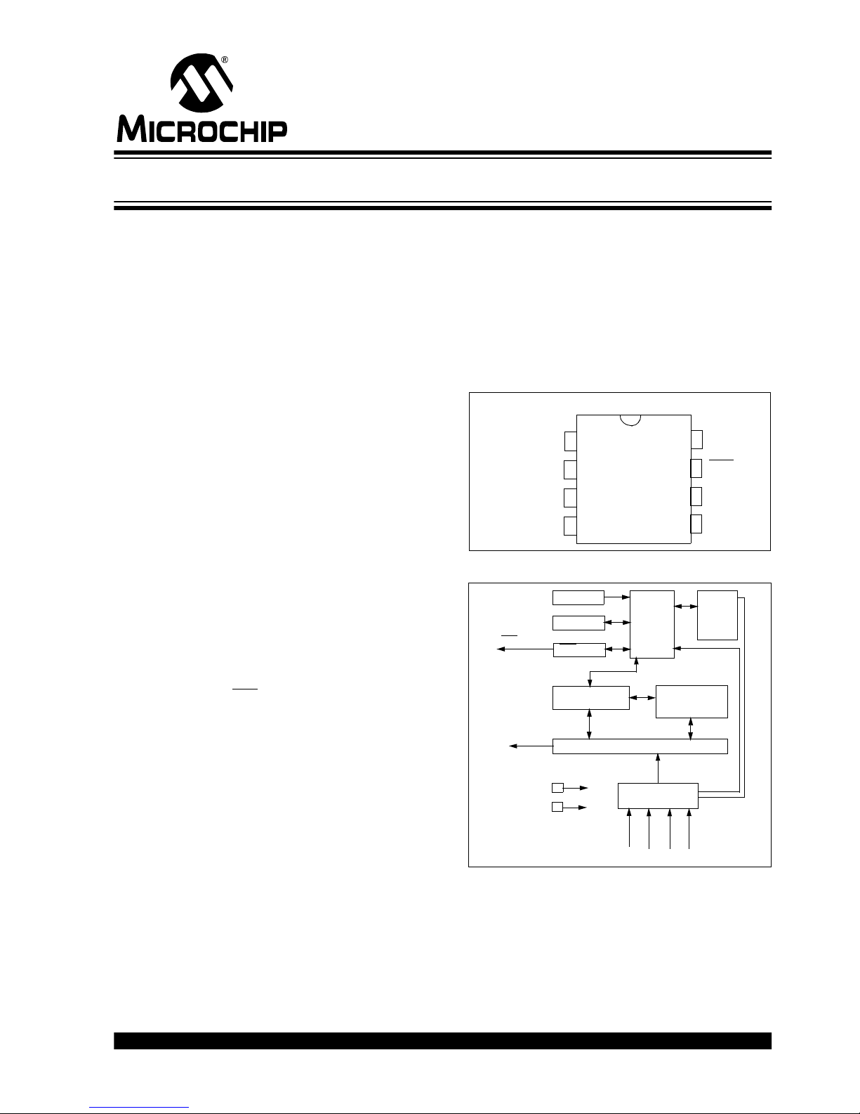
PACKAGE TYPES
PDIP, SOIC
8
S0
S1
S2
S3
1
HCS300
2
3
4
VDD
LED
7
6
PWM
V
SS
5
HCS300 BLOCK DIAGRAM
LED
PWM
Oscillator
Reset circuit
VSS
VDD
LED
EEPROM
driver
Controller
32-bit shift register
Button input port
S
S
2
3
Encoder
S1S
0
Power
latching
and
switching
KEELOQ is a registered trademark of Microchip Technology, Inc.
Microchip’s Secure Data Products are covered by some or all of the following patents:
Code hopping encoder patents issued in Europe, U.S.A., and R.S.A. — U.S.A.: 5,517,187; Europe: 0459781; R.S.A.: ZA93/4726
1999 Microchip Technology Inc. Preliminary DS21137E-pa ge 1
Page 2

HCS300
The HCS300 combines a 32-bit hopping code
generated by a non-linear enc r y ption algorithm, with a
28-bit serial number and six status bits to create a 66bit transmission stream. The length of the transmission
eliminates the threat o f code scanning and the code
hopping mechanism makes each transmission unique,
thus rendering code captur e and resend (code grabbing) schemes useless.
The encryptio n key, serial number, and configuration
data are stored in EEPROM, which is not accessible via
any external connection. This makes the HCS300 a
very secure unit. The HCS300 provides an easy to use
serial interface for programming the necessary security
keys, system parameters, and configuration data.
The encyrption keys and code combinations are programmable but read-protected. The keys can only be
verified after an automatic erase and programming
operation. This protects against attempts to gain
access to keys and manipulate synchronization values.
The HCS300 operates over a wide voltage range of
2.0V to 6.3V and has four button inputs in an 8-pin
configuration. This allows the system designer the
freedom to utilize up to 15 functions. The only
components required for device operation are the buttons and RF circuitry, allowing for a very low
system cost.
1.0 SYSTEM OVERVIEW
Key Terms
• Manufacturer’s code - a 64-bit word, unique to
each manufacturer, used to produce a unique
encryption key in each transmitter (encoder).
• Encryption Key
and programmed into the encoder during the
manufacturing process. The encryption key
controls the encryption algorithm and is stored in
EEPROM on the encoder device.
1.1 Learn
The HCS product family facilitates several learn strategies to be implemented on the decoder. The following
are examples of what can be done. It must be pointed
out that there exists some third-party patents on learning strategies and implementation.
1.1.1 NORMAL LEAR N
The receiver uses the same information that is transmitted during no rmal operation to derive the transmitter’s secret key, decrypt the discr imination value and
the synchronization counter.
- a unique 64-bit key generated
1.1.2 SECURE LEARN*
The transmitter is activated through a special button
combination to transmit a stored 48-bit value (random
seed) that can be used for key generation or be part of
the key. Transmission of the random seed can be disabled after learning is completed.
The HCS300 is a code hopping encoder device that is
designed specifically for keyless entry systems,
primarily for vehicles and home garage doo r openers.
It is meant to be a cost-effective, yet secure solution to
such systems. The encoder por tion of a keyless entry
system is meant to be held by the user and operated to
gain access to a vehicle or restricted area. The
HCS300 requires very few external components
(Figure 2-1).
Most keyless entry systems transmit the same code
from a transmitter every time a button is pushed. The
relative number of code combinations for a low end
system is also a relatively small number. These
shortcomings provide the means for a sophisticated
thief to create a device that ‘grabs’ a transmission and
re-transmits it later or a device that scans all possible
combinations until the correct one is found.
The HCS300 employs the code hopping technology
and an encrypti on algorithm to achieve a high level of
security. Code hopping is a method by which the code
transmitted from the transmitter to the receiver is
different every time a button is pushed. This method,
coupled with a transmission length of 66 bits, virtually
eliminates the use of code ‘grabbing’ or code
‘scanning’.
As indicated in the block diagram on page one, the
HCS300 has a small EEPROM array which must be
loaded with several parameters before use. The most
important of these values are:
• A 28-bit serial number which is meant to be
unique for every encoder.
• An encryption key that is generated at the time of
production.
• A 16-bit synchronization value.
The serial number for each transmitter is programmed
by the manufacturer at the time of production. The
generation of the encry ption key is done using a key
generation algorithm (Figure 1-1). Typically, inputs to
the key generation algorithm are the serial number of
the transmitter and a 64-bit manufacturer’s code. The
manufacturer’s code is chosen by the system
manufacturer and must be carefully controlled. The
manufacturer’s code is a pivotal part of the overall
system security.
DS21137E-pag e 2 Preliminary 1999 Microchip Technology Inc.
Page 3
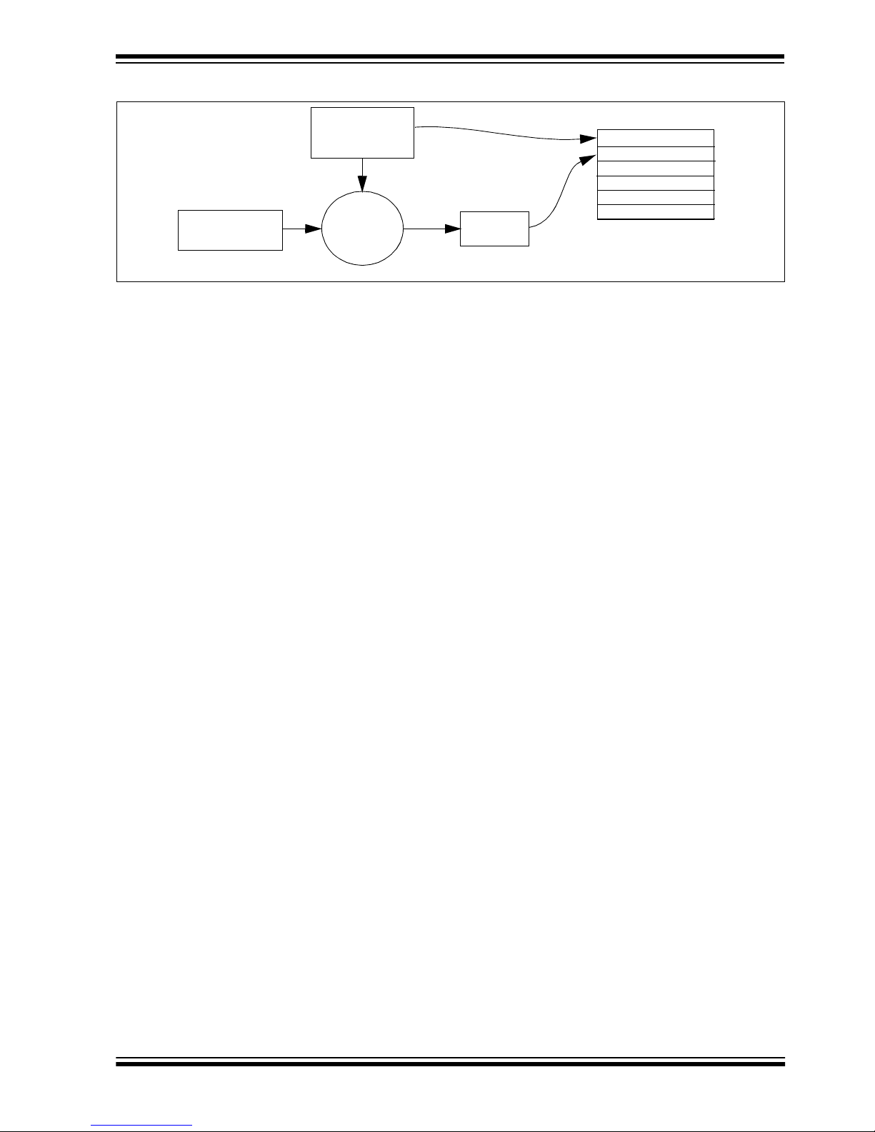
FIGURE 1-1: CREATION AND STORAGE OF ENCRYPT ION KEY DURING PRODUCTION
HCS300
Transmitter
Serial Number or
Seed
Manufacturer’s
Code
The 16-bit synchronization value is the basis for the
transmitted code changing for eac h transmission, and
is updated each time a button is pressed. Because of
the complexity of the code hopping encryption algorithm, a change in one bit of the s ync hronization value
will result in a large change in the actual transmitted
code. There is a relationsh ip (Figure 1-2) between the
key values in EEPROM and how they are used in the
encoder. Once the encoder detects that a button has
been pressed, the encoder reads the button and
updates the synchronization counter. The synchronization value is then combined with the encr yption key in
the encryption algor ithm and the output is 32 bits of
encrypted information. This data will change with every
button press, hence, it is referred to as the hopping
portion of the code word. The 32-bit hopping c ode is
combined with the button information and the serial
number to form the code word transmitted to the
receiver. The code word format is explained in detail
in Section 4.2.
Key
Generation
Algorithm
HCS300 EEPROM Array
Serial Number
Encryption Key
Sync Counter
.
.
Encryption
Key
Any type of controller may be used as a receiver, but it
is typically a microcontr oller with compatible firmware
that allows the receiver to operate in conjunction with a
transmitter, based on the HCS300. Section 7.0
provides more detail on integrating the HCS3 00 into a
total system.
Before a transmitter can be used with a particular
receiver, the transmitter must be ‘learned’ by the
receiver. Upon learning a transmitter, information is
stored by the receiver so that it may track the
transmitter, including the serial number of the
transmitter, the current synchronization value for that
transmitter and the same encryption key that is used on
the transmitter. If a receiver receives a message of valid
format, the serial number is checked and, if it is from a
learned transmitter, the message is decrypted and the
decrypted synchroni zation counter is checked against
what is stored. If th e synchronization value is verified,
then the button status is checked to see what operation
is needed. Figure 1-3 shows the relationship between
some of the values stored by the receiver and the values received from the transm itter.
.
1999 Microchip Technology Inc. Preliminary DS21137E-pa ge 3
Page 4
HCS300
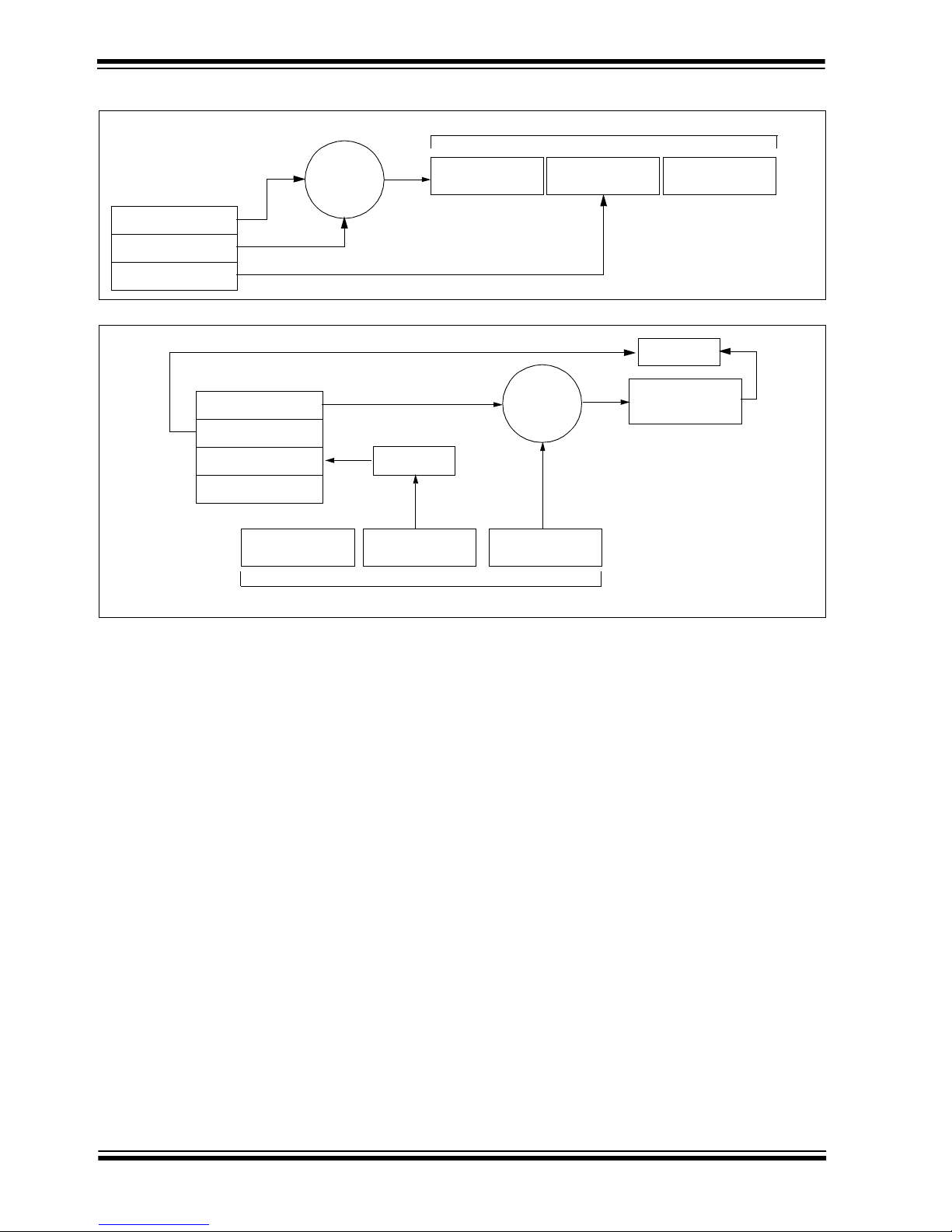
FIGURE 1-2: BASIC OPERATION OF TRANSMITTER (ENCODER)
Transmitted Information
KEELOQ
Encryption
EEPROM Array
Encryption Key
Sync Counter
Serial Number
FIGURE 1-3: BASIC OPERATION OF RECEIVER (DECODER)
EEPROM Array
Encryption Key
Sync Counter
Serial Number
Manufacturer Code
Button Press
Information
Algorithm
Check for
Match
Serial Number
Received Information
32 Bits of
Encrypted Data
Serial Number
KEELOQ
Decryption
Algorithm
32 Bits of
Encrypted Data
Button Press
Information
Check for
Match
Decrypted
Synchronization
Counter
DS21137E-pag e 4 Preliminary 1999 Microchip Technology Inc.
Page 5
HCS300
2.0 DEV ICE OPERATION
As shown in the typical application circuits (Figure 2-1),
the HCS300 is a simple device to use. It requ ires only
the addition of buttons and RF circuitry for use as the
transmitter in your security application. A description of
each pin is described in Table 2-1.
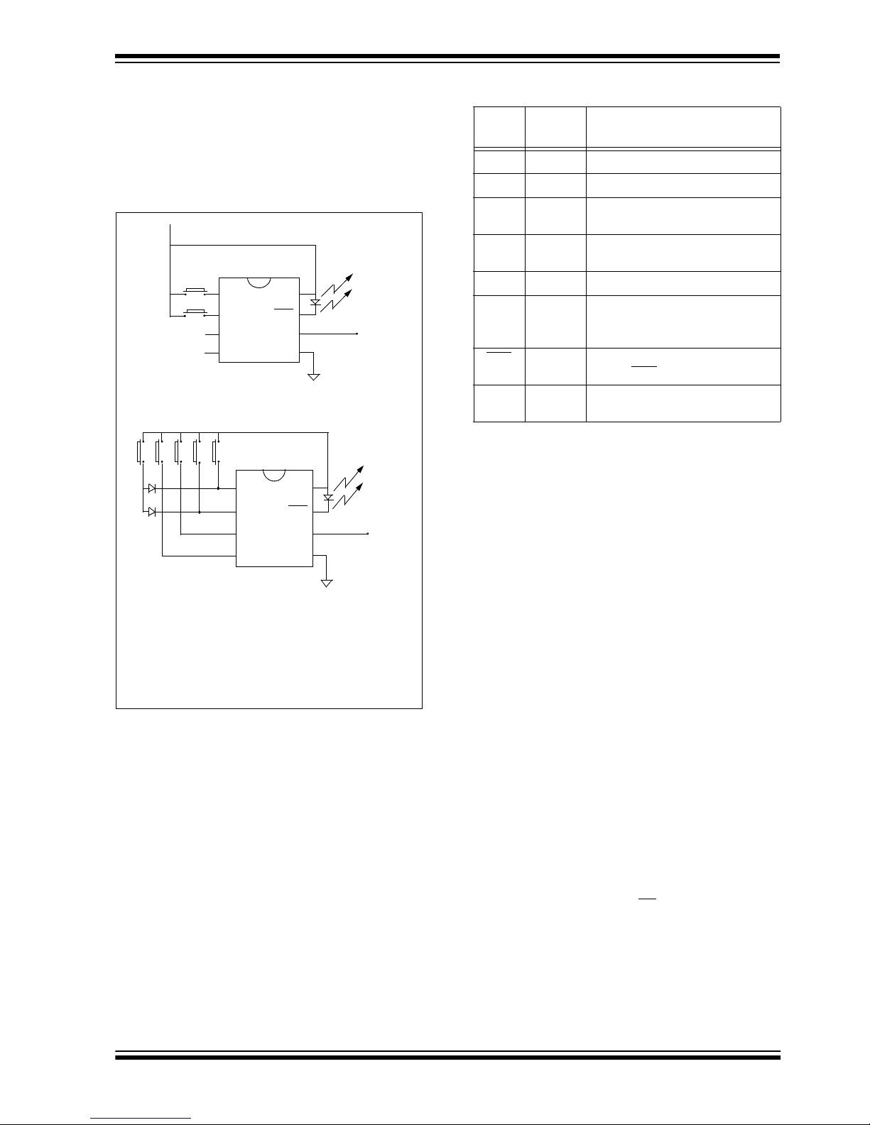
FIGURE 2-1: TYPICAL CIRCUITS
VDD
B0
B1
B4 B3 B2 B1 B0
Note: Up to 1 5 fu nc tio ns c a n be imp l em e nte d by pre s s-
S0
S1
S2
S3
2 button remote control
5 button remote control (Note)
ing more than one button simultaneously or by
using a suitable diode array.
S0
S1
S2
S3
VDD
LED
PWM
SS
V
VDD
LED
PWM
SS
V
Tx out
VDD
Tx out
TABLE 2-1: PIN DESCRIPTIONS
Name
S0 1
S1 2
S2 3
Pin
Number
Description
Switch input 0
Switch input 1
Switch input 2/Can also be c lock
pin when in programming mode
S3 4
Switch input 3/Clock pin when in
programming mode
V
SS 5
PWM 6
Ground reference connection
Pulse width modulation (PWM)
output pin/Data pin for
programming mode
LED
VDD
Cathode connection for directly
7
driving LED
Positive supply voltage
8
during transmission
connection
The high security l evel of the HCS300 is bas ed on the
patented
technology. A block cipher type of encryption
algorithm based on a block length of 32 bits and a key
length of 64 bits is used. The algorithm obscure s the
information in such a way that even if the transmission
information (before coding ) differs by only one bit from
the information in the p revious transmission, the next
coded transmission will be totally different. Statistically,
if only one bit in the 32-bit string of information
changes, approximately 50 percent of the coded transmission will change. Th e HCS300 will wake up upon
detecting a switch closure and then delay approximately 10 ms for switch debounce (Figure 2-2). The
synchronized information, fixed information, and switch
information will be encrypted to form the hopping code.
The encrypted or hopping code portion of the transmission will change every time a button is pressed, even if
the same button is pushed again. Keeping a button
pressed for a long time will result in the same code
word being transmitted, until the button is re leased or
timeout occurs. A code that has been transmi tted will
not occur again for more than 64K transmissions. This
will provide more than 18 years of typical use before a
code is repeated, based on 10 operations per day.
Overflow information programmed into the encoder can
be used by the decoder to extend the number of unique
transmissions to more than 192K.
If in the transmit process it i s detected that a new button(s) has been press ed, a reset will immediately be
forced and the code word will not
be completed. Please
note that buttons removed will not have any effect on
the code word unless no buttons remain pressed in
which case the current code word wi ll be completed
and the power down will occur.
1999 Microchip Technology Inc. Preliminary DS21137E-pa ge 5
Page 6
HCS300
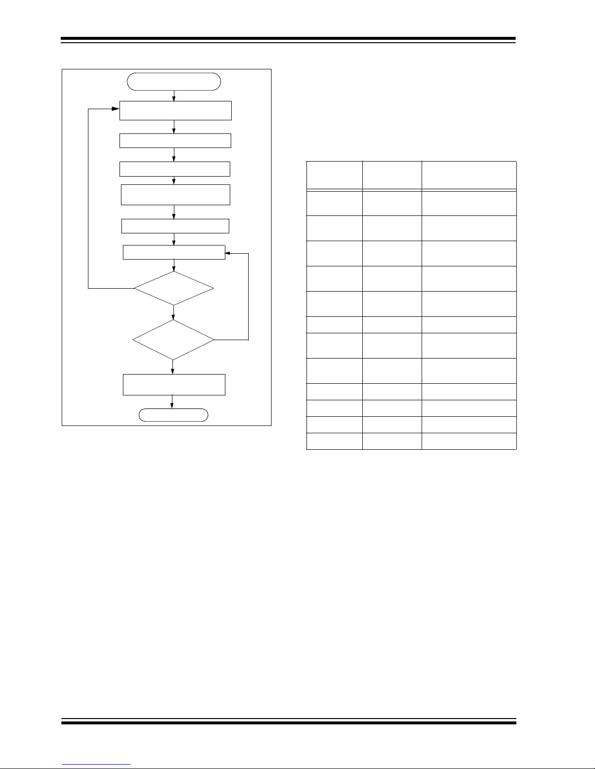
FIGURE 2-2: ENCODER OPERATION
Power Up
(A button has been pressed)
Reset and Debounce Delay
(10 ms)
Sample Inputs
Update Sync Info
Encrypt With
Encryption Key
Load Transmit Register
Transmit
Yes
Buttons
Added
?
No
All
Buttons
Released
?
Yes
Complete Code
Word Transmission
Stop
No
3.0 EEPROM MEMOR Y
ORGANIZATION
The HCS300 contains 192 bits (12 x 16-bit words) of
EEPROM memory (Table 3-1). This EEPROM array is
used to store the encryption key information,
synchronization value, etc. Fur ther descr iptions of the
memory array is given in the following sections.
TABLE 3-1: EEPROM MEMORY MAP
WORD
ADDRESS
0
1
2
3
4
5
6
7
8
9
10
11
Note: The MSB of the serial number contains a bit
MNEMONIC DESCRIPTION
KEY_0 64-bit encryption key
(word 0)
KEY_1 64-bit encryption key
(word 1)
KEY_2 64-bit encryption key
(word 2)
KEY_3 64-bit encryption key
(word 3)
SYNC 16-bit synchronization
value
RESERVED Set to 0000H
SER_0 Device Serial Number
(word 0)
SER_1(Note) Device Serial Number
(word 1)
SEED_0 Seed Value (word 0)
SEED_1 Seed Value (word 1)
EN_KEY 16-bit Envelope Key
CONFIG Config Word
used to select the auto shutoff timer.
DS21137E-pag e 6 Preliminary 1999 Microchip Technology Inc.
3.1 Key_0 - Key_3 (64-Bit Encryption Ke y)
The 64-bit encrypti on key is used by the transmitter to
create the encrypted message transmitted to the
receiver. This key is created and programmed at the
time of production using a key generation algorithm.
Inputs to the key generation algorithm are the serial
number for the par tic ular transmitter b eing us ed and a
secret manufacturer’s code. While the key generation
algorithm supplied is the typical method used, a user
may elect to create their own method of key generation.
This may be done, providing that the decoder is programmed with the same means of creating the key for
decryption purposes. If a seed is used, the seed will
also form par t of the input to the key generation algorithm.
Page 7

HCS300
3.2 SYNC (Synchronization Counter)
This is the 16-bit synchroni zation value that is us ed to
create the hopping code for transmission. Thi s val ue
will be changed after every transmission.
3.3 SER_0, SER_1 (Encoder Serial
Number)
SER_0 and SER_1 are the lower and u pper words of
the device serial number, respectively. Although there
are 32 bits allocated for the serial number, only the
lower order 28 bits are transmitted. Th e serial num ber
is meant to be un ique for every transmitter. The most
significant bit of the serial number (Bit 31) is used to
turn the auto shutoff ti mer on or off.
3.3.1 AUTO SHUTOFF TIMER SELECT
The most significant bit of t he ser ial number (Bit 31) is
used to turn the Auto shutoff timer on or off. This timer
prevents the transmitter from draining the battery
should a button get stuck in the on position for a long
period of time. The time period is approximately
25 seconds, after which the device will go to the Timeout mode. When in the Time-out mode, the device will
stop transmitting, although since some circuits with in
the device are still active, the current draw within the
Shutoff mode will be more than Standby mode. If the
most significant bit in the seria l number is a one, then
the auto shutoff timer is enabled, and a zero in the most
significant bit will disable the timer. The length of the
timer is not selectable.
3.4 SEED_0, SEED_1 (Seed Word)
This is the two word (32 bits) seed code tha t will be
transmitted when all four buttons are pressed at the
same time. This allows the system designer to implement the secure learn feature or use this fixed code
word as part of a different key generation/tracking process or purely as a fixed code transmission.
3.5 EN_Key (Envelope Encryption Key)
Envelope encryption is a selectable option that
encrypts the por tion of the transmission that contains
the transmitter serial number. Selecting this option is
done by setting the appropriate bit in the configuration
word (Table 3-2). Normally, the serial number is
transmitted in the clear (un-encrypted), but for an
added level of security, the system designer may elect
to implement this option. The envelope encryption key
is used to encrypt the serial number portion of the
transmission, if the envelope encryption option has
been selected. The envelope encryption algorithm i s a
different algorithm than the key generation or transmit
encryption algorithm. The EN_key is typically a random
number and the same for all transmitters in a system.
3.6 Configuration Word
The configuration word is a 16-bit word stored in
EEPROM array that is used by the device to store
information used during the encryption process, as well
as the status of option configurations. Further
explanations of each of the bits are described in the
following sections.
TABLE 3-2: CONFIGURATION WORD
Bit Number Bit Description
0
1
2
3
4
5
6
7
8
9
10
11
12
13
14
15
3.6.1 DISCRIMINATION VALUE
The discrimination value can be pr ogrammed with a ny
value to serve as a post decryption check on the
decoder end. In a typical system, this will be
programmed with the 10 least significant bits of the
serial number, which will also be stored by the receiver
system after a transmitter has been learned. The
discrimination bits a re part of the infor m ation th at i s to
form the encrypted por tion of the transmission. After
the receiver has decrypted a transmission, the
discrimination bits c an be checked against the stored
value to verify that the decryption process was valid.
3.6.2 OVERFLOW BITS (OVR0 AND OVR1)
The overflow bits are used to extend the number of pos-
sible synchronization values. The synchronization
counter is 16 bits in length, yielding 65,536 values
before the cycle repeats. Under typical use of
10 operations a day, this will provide nearly 18 years of
use before a repeated value will b e used. Should the
system designer conclude that is not adequate, then
the overflow bits can be utilized to extend the number
of unique values. This can be done by programming
OVR0 and OVR1 to 1s at the time of produc tion. The
encoder will automatically clear OVR0 the first time that
the synchronization value wraps from 0xFFFF to
Discrimination Bit 0
Discrimination Bit 1
Discrimination Bit 2
Discrimination Bit 3
Discrimination Bit 4
Discrimination Bit 5
Discrimination Bit 6
Discrimination Bit 7
Discrimination Bit 8
Discrimination Bit 9
Overflow Bit 0 (OVR0)
Overflow Bit 1 (OVR1)
Low Voltage Trip Point Select
Baudrate Select Bit 0 (BSL0)
Baudrate Select Bit 1 (BSL1)
Envelope Encryption Select (EENC)
(DISC0 TO DISC9)
1999 Microchip Technology Inc. Preliminary DS21137E-pa ge 7
Page 8
HCS300
0x0000 and clear OVR1 the second time the counter
wraps. Once cleared, OVR0 and OVR1 cannot be set
again, thereby creating a permanent record of the
counter overflow. This prevents fast cycling of 64K
counter. If the decoder system is programmed t o track
the overflow bits, then the effective number of unique
synchronization values can be extended to 196,608. If
programmed to zero, the system will be compatible with
the NTQ104/5/6 devices (i.e., no overflow with discrimination bits set to zero).
3.6.3 ENVELOPE ENCRYPTION (EENC)
If the EENC bit is set to a 1, the 32-bit fixed code par t
of the transmission will also be encrypted so that it will
appear to be random. The 16-bit envelope key and
envelope algorithm will be used for encryption.
3.6.4 BAUDRATE SELECT BITS (BSL0, BSL1)
BSL0 and BSL1 select the speed of transmission and
the code word blanking. Table 3-3 shows how the bits
are used to select the different baud rates and
Section 5.2 provides detailed explanation in code word
blanking.
TABLE 3-3: BAUDRATE SELECT
BSL1 BS L0
Basic Pulse
Element
Code Words
Transmitted
0 0 400µs All
0 1 200µs 1 out of 2
1 0 100µs 1 out of 2
1 1 100µs 1 out of 4
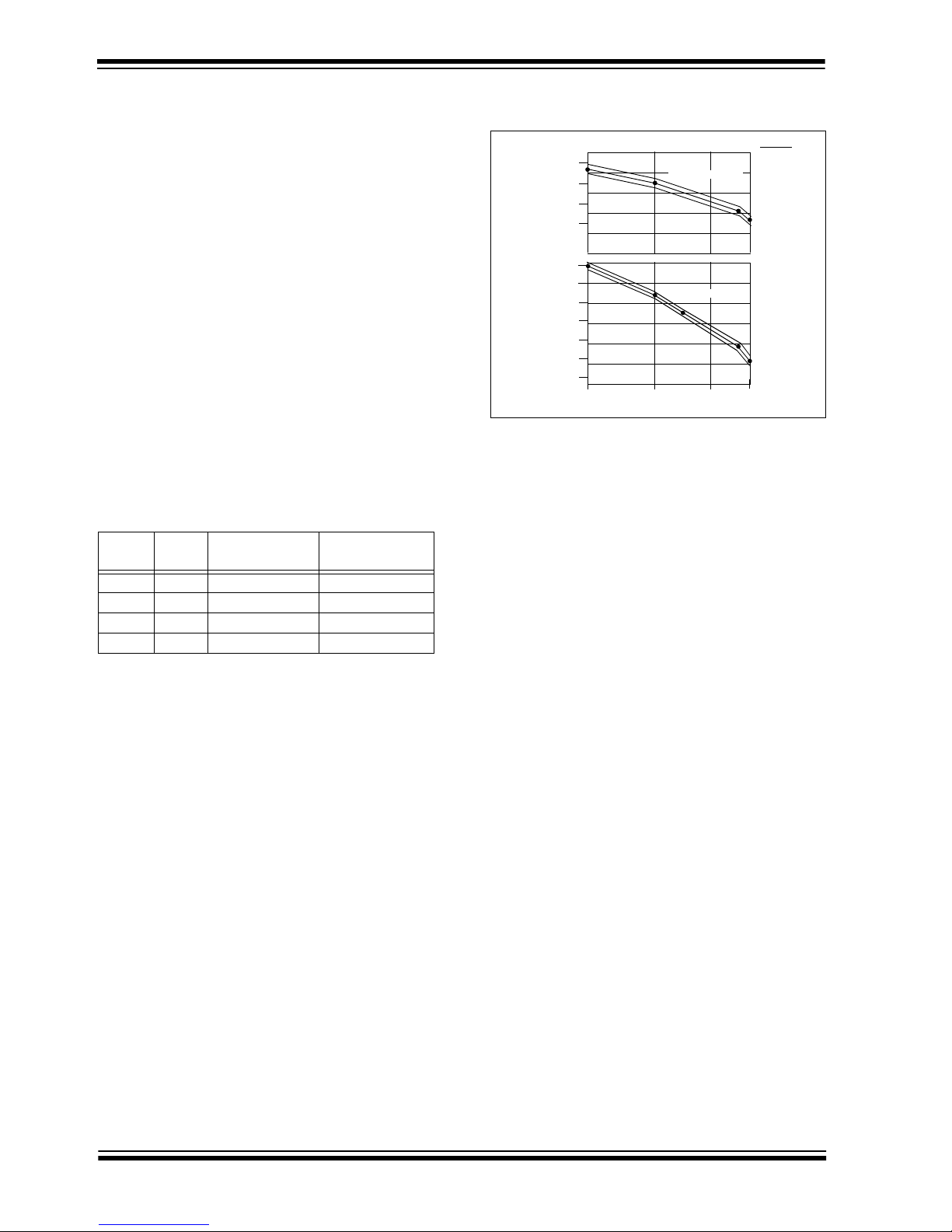
3.6.5 LOW VOLTAGE TRIP POINT SELECT
The low voltage trip point select b it is used to tell the
HCS300 what
VDD level is being used. This information
will be used by the device to deter mine when to send
the voltage low signal to the receiver. When this bit is
set to a one, the
from a 5 volt or 6 volt
the
VDD level is assumed to be 3.0 volts. Refer to
VDD level is assumed to be operating
VDD level . If the bit is set l ow, then
Figure 3-1 for voltage trip point.VLOW is tested at 6.3V
at -25°C and +85°C and 2.0V at -25°C and +85°C
FIGURE 3-1: TYPICAL VOLTAGE TRIP
POINTS
Volts (V)
4.2
4.0
3.8
3.6
2.6
2.4
2.2
2.0
1.8
1.6
1.4
-40
VLOW sel = 1
VLOW sel = 0
05085
VLOW
Temp (C )
4.0 TRANSMITTED WORD
4.1 Transmission Format (PWM)
The HCS300 transmission is made up of several parts
(Figure 4-1). Each transmission is begun with a
preamble and a header, followed by the encrypted and
then the fixed data. The actual data is 66 bits which
consists of 32 bits of encrypted data and 34 bits of fixed
data. Each transmission is followed by a guard period
before another transmission can begin. Refer to
Table 8-4 for transmission timing requirements. The
encrypted portion p rovides up to four bill ion changing
code combinations and includes the button status bits
(based on which buttons were activated) along with the
synchronization counter value and some discrimination
bits. The fixed portion is comp rised of the status bits,
the function bits and the 28-bit serial number. The fixed
and encrypted sections combined increase the number
of combinations to 7.38 x 10
4.2 Synchronous Transmission Mode
Synchronous transmission mode can be u sed to clock
the code word out using an external clock.
To enter synchronous transmission mode, the programming mode start- up sequence must be executed
as shown in Figure 4-3. If either S1 or S0 is set on the
falling edge of S2 (or S3), the device enters synchronous transmission mode. In this mode, it functions as a
normal transmitter, with the exception that the timing of
the PWM data string is controlled externally and 16
extra bits are transmitted at the end with the code word.
The button code will be the S0, S1 value at the falling
edge of S2 or S3. The timing of the PWM data string is
controlled by supplying a clock on S2 or S3 and should
not exceed 20 kHz. The code word is the same as in
PWM mode with 16 reserved bits at the end of the
word. The reserved bits can b e ignored. When in syn-
19
.
DS21137E-pag e 8 Preliminary 1999 Microchip Technology Inc.
Page 9

chronous transmission mode S2 or S3 should not be
toggled until all internal processing has been completed as shown in Figure 4-4.
4.3 Code Word Organization
The HCS300 transmits a 66-bit code word when a button is pressed. The 66-bit word is constructed from a
Fixed Code portion and an Encrypted Code portion
(Figure 4-2).
The Encrypted Data is generated from four button bits,
two overflow counter bits, ten discrimination bits, and
the 16-bit synchronization value (Figure 8-4).
The Fixed Code Data is made up from two status bits,
four button bits, and the 28-bit serial number. The four
button bits and the 28-bit serial number may be
encrypted with the Envelope Key, if the envelope
encryption is enabled by the user.
FIGURE 4-1: CODE WORD TRANSMISSION FORMAT
LOGIC ‘0’
HCS300
LOGIC ‘1’
Bit
Period
Preamble
TP
FIGURE 4-2: CODE WORD ORGANIZATION
Fixed Code Data
VLOW and
Repeat Status
(2 bits)
2 bits
of Status
Button
Status
(4 bits)
Serial Number and Button
+
Header
TH
28-bit Serial Number
Status (32 bits)
Encrypted Portion
of Transmission
THOP
Button
Status
(4 bits)
Overflow
+
Fixed Portion of
Transmission
Encrypted Code Data
bits
(2 bits)
BLOCK CIPHER
32 bits of Encrypted Data
TFIX
Discrimination
bits
(10 bits)
Encrypted using
Algorithm
Transmission Direction
Guard
Time
TG
16-bit
Sync Value
1999 Microchip Technology Inc. Preliminary DS21137E-pa ge 9
Page 10

HCS300
FIGURE 4-3: SYNCHRONOUS TRANSMISSION MODE
t = 50 ms
PWM
S2(S3)
S[1:0]
FIGURE 4-4: TRANSMISSION WORD FORMAT DURING SYNCHRONOUS TRANSMISSION MODE
Reserved Padding
“01,10,11”
Button
Code
Serial Number Data Word Sync Counter
16 2 4 28 16 16
Transmission Direction
5.0 SPECIAL FEATURES
5.1 Code Word Completion
Code word completion is an automatic feature that
makes sure that the entire code word is transmitted,
even if the button is released before the transmission is
complete. The HCS300 encoder powers itself up when
a button is pushed and powers itself down after the
command is finished, if the user has already released
the button. If the button is held down beyond the time
for one transmission, then multiple transmissions wi ll
result. If another button is activated during a
transmission, the active transmission will be abor ted
and the new code will be generated using the new
button information.
5.2 Blank Alternate Code Word
Federal Communications Commission (FCC) Part 15
rules specify the limits on fundamental power and
harmonics that can be transmitted. Power is calculated
on the worst case average power transmitted in a
100ms window. It is therefore advantageous to
minimize the duty cycle of the transmitted word. This
can be achieved by minimizing the duty cycle of the
individual bits and by blanking out consecutive words.
Blank Alternate Code Word (BACW) is used for
reducing the average power of a transmission
(Figure 5-1). This is a selectable feature that is
determined in conjunction wi th the baudrate selection
bits BSL0 and BSL1. Using the BACW allows the user
to transmit a higher amplitude transmission if the
transmission length is shorter. The FCC puts
constraints on the average power that can be
transmitted by a device, and BACW effectively prevents
continuous transmission by only allowing the transmission of every second or every fourth code word. This
reduces the average power transmitted and hence,
assists in FCC approval of a transmitter device.
5.3 Envelope Encryption Option
Envelope Encryption is a user selectable option which
is meant to offer a highe r level of security for a code
hopping system. During a normal transmission with the
envelope encryption turned off, the 28-bit serial
number is transmitted in the clear (unencrypted). If
envelope encryption is selected, then the serial number
is also encrypted before transmission. The en crypt ion
for the serial number is done using a different algorithm
than the transmission algorithm. The envelope
encryption scheme is not nearly as complex as the
algorithm and, henc e, not as secure. When the envelope encryption is used, the serial number must be
decrypted using the envelope key and envelope
decryption. After the serial number is obtained, the normal decryption method can be used to decrypt the hopping code. All transmitters in a system must use the
same envelope key.
5.4 Secure Learn
In order to increase the l evel of security in a s ystem, it
is possible for the receiver to implement what is known
as a secure learn function. This can be done by utilizing
the seed value on the HCS300 which is stored in
EEPROM and can only be transmitted when all four
DS21137E-pag e 10 Preliminary 1999 Microchip Technology Inc.
Page 11

HCS300
button inputs are pressed at the same time (Table 5-1).
Instead of the normal key generation method being
used to create the encr yption key, this seed value is
used and there need not be any mathematical relationship between serial numbers and seeds.
TABLE 5-1: PIN ACTIVATION TABLE
S3 S2 S1 S0 Notes
1
2
3
4
5
6
7
8
9
10
11
12
13
14
15
Note 1: Transmit generated 32-bit code
000 1 1
001 0 1
001 1 1
010 0 1
010 1 1
011 0 1
011 1 1
100 0 1
100 1 1
101 0 1
101 1 1
11 0 0 1
110 1 1
111 0 1
111 1 2
hopping word.
2: Transmit 32-bit seed value.
5.5 Auto-shutoff
The Auto-shutoff function automatically stops the
device from transmitting if a button inadvertently gets
pressed for a long peri od of time. Thi s will prevent the
device from draining the battery if a button gets pressed
while the transmitter is in a pocket or purse. This function can be enabled or disabled and is selected by setting or clearing the Auto-shutoff bit (see Section 3.3.1).
Setting this bit high will enable the function (turn Autoshutoff function on) and setting the bit low will disable
the function. Time-out pe riod is approximately 25 seconds.
FIGURE 5-1: BLANK ALTERNATE CODE WORD (BACW)
Amplitude
100ms
BACW Disabled
(All words transmitted)
BACW Enabled
(1 out of 2 transmitted)
BACW Enabled
(1 out of 4 transmitted)
1999 Microchip Technology Inc. Preliminary DS21 137E-page 11
A
2A
4A
100ms
One Code Word
Time
100ms
100ms
Page 12

HCS300
5.6 VLOW: Voltage LOW Indicator
The VLOW bit is transmitted with every transmission
(Figure 8-4) and will be transmitted as a one if the
operating voltage has dropped below the low voltage
trip point. The trip point is selectable between two
values, based on the battery voltage being used. See
Section 3.6.5 for a description of how the low voltage
select option is set. This VLOW signal is transmitted so
the receiver can give an audible signal to the user that
the transmitter battery is low (Section 5.8).
5.7 RPT: Repeat Indicator
This bit will be low for the first transmitted word. If a
button is held down for more than one transmitted code
word, this bit will be set to indicate a repeated code
word and remain set until the button is released
(Figure 8-4).
5.8 LED Output Operation
During nor mal transmission the LED output i s LOW. If
the supply voltage drops below the low voltage trip
point, the LED
5Hz during the transmission (Section 3.6.5).
output will be toggled at approximately
DS21137E-pag e 12 Preliminary 1999 Microchip Technology Inc.
Page 13

HCS300
6.0 PROGRAMMING THE HCS300
When using the HCS300 in a system, the user will have
to program some parameters into the device including
the serial number a nd the secret key before it can be
used. The programming cycle allows the user to i nput
all 192 bits in a serial data stream, which are then
stored internally in EEPROM. Programming will be
initiated by forcing the PWM line high, after the S3 line
has been held high for the appropriate length of time
line (T able 6-1 and Figure 6-1). After the program mode
is entered, a delay must be provided to the device for
the automatic bulk write cycle to complete. This will
write all locations in the EEPROM to an all zeros pattern. The device can then be programmed by clocking
in 16 bits at a time, using S3 as the clock line and PWM
FIGURE 6-1: PROGRAMMING WAVEFORMS
S3
(Clock)
PWM
(Data)
Enter Program
Mode
TPS
TPH1
TPBW
TCLKH
TCLKL
Bit 0 Bit 1 Bit 2 Bit 3 Bit 14 Bit 15 Bit 16 Bit 17
TDS
TDH
as the data in line. After each 16-bit word is loaded, a
programming delay is required for the internal program
cycle to complete. This delay can tak e up to T
end of the programming cycle, the device can be verified (Figure 6-2) by reading back the EEPROM. Reading is done by clocking the S3 line and reading the data
bits on PWM. For security reasons, it is not possible to
execute a verify function without first programming the
EEPROM. A verify operation can only be done
once, immediately following the program cycle.
Note: To ensure that t he device does not acci-
dentally enter programming mode, PWM
should never be pulled high by the circuit
connected to it. Special care should be
taken when driving PNP RF transistors.
TWC
WC. At the
TPH2
Note 1: Unused button inputs to be held to ground du ring the entire programming sequence.
Note 2: The VDD pin must be taken to ground after a program/verify cycle.
FIGURE 6-2: VERIFY WAVEFORMS
End of
Programming Cycle
PWM
(Data)
S3
(Clock)
Note: If a Verify operation is to be done, then it must immediately follow the Program cycle.
Begin Verify Cycle Here
Bit 0Bit191Bit190
TWC
Bit 1 Bit 2 Bit 3 Bit 15Bit 14 Bit 16 Bit 17 B it190 Bit191
Data for Word 0 (KEY_0)
Repeat 12 times for each word
Data in Word 0
TDV
Data for Word 1
1999 Microchip Technology Inc. Preliminary DS21 137E-page 13
Page 14

HCS300
TABLE 6-1: PROGRAMMING/VERIFY TIMING REQUIREMENTS
VDD = 5.0V ± 10%
25° C ± 5 °C
Parameter Symbol Min. Max. Units
Program mode setup time
Hold time 1
Hold time 2
Bulk Write time
Program delay time
Program cycle time
Clock low time
Clock high time
Data setup time
Data hold time
Data out valid time
T
PS 3.5 4.5 ms
PH1 3.5 — ms
T
PH2 50 — µs
T
T
PBW — 2.2 ms
PROG — 2.2 ms
T
WC —36ms
T
CLKL 25 — µs
T
CLKH 25 — µs
T
DS 0—µs
T
DH 18 — µs
T
DV 10 24 µs
T
DS21137E-pag e 14 Preliminary 1999 Microchip Technology Inc.
Page 15

HCS300
7.0 INTEGRATING THE HCS300
INTO A SYSTEM
Use of the HCS300 in a system requires a co mpatible
decoder. This decoder is typically a microcontroller with
compatible firmware. Microchip will provide (via a
license agreement) firmware routines that accept
transmissions from the HCS300 and decrypt the
hopping code portion of the data stream. These
routines provide system designers the means to
develop their own decoding system.
7.1 Learning a Transmitter to a Receiver
In order for a transmitter to be used with a decoder, the
transmitter must first be ‘learned’. Several learning
strategies can be followed in the decoder implementation. When a transmitter is learned to a decoder, it is
suggested that the decoder stores the s erial number
and current synchronization value in EEPROM. The
decoder must keep track of these values for every
transmitter that is learned (Figure 7-1). The maximum
number of transmitters that c an be learned is only a
function of how much EEPROM memory storage is
available. The decoder must also store the manufacturer’s code in order to learn a transmission transmitter,
although this value will not change in a typical system
so it is usually stored as part of the microcontroller
ROM code. Storing the manufacturer’s code as part of
the ROM code is also better for security reasons.
It must be stated that some learning strategies have
been patented and care must be taken not to infringe.
FIGURE 7-1: TYPICAL LEARN SEQUENCE
Enter Learn
Mode
Wait for Reception
of a Valid Code
Generate Key
from Serial Number
Use Generated Key
to Decrypt
Compare Discrimination
Value with Fixed Value
Equal
?
Yes
Wait for Reception
of Second Valid Code
Use Generated Key
to Decrypt
Compare Discrimination
Value with Fixed Value
Equal
?
Yes
No
No
Counters
Sequential
?
Yes
Learn successful Store:
Serial number
Encryption key
Synchronization counter
Exit
No
Learn
Unsuccessful
1999 Microchip Technology Inc. Preliminary DS21 137E-page 15
Page 16

HCS300
7.2 Decoder Operation
In a typical decoder operation (Figure 7-2), the key
generation on the decoder side is done by taking the
serial number from a transmissio n and combi ning that
with the manufacturer’s code to create the same secret
key that was used by the transmitter. Once the secret
key is obtained, the rest of the transmission can be
decrypted. Th e decoder waits for a transmission and
immediately can check the serial number to determine
if it is a learned transmitter. If it is, it takes the encrypted
portion of the transmission and decrypts it using the
stored key. It uses the discr imination b its to deter mine
if the decryption was valid. If everything up to this point
is valid, the synchronization value is evaluated.
FIGURE 7-2: TYPICAL DECODER OPERATION
Start
No
Transmission
Received
?
Yes
No
Decrypt Transmission
No
No
No
Does
Serial Number
Match
?
Yes
Is
Decryption
Valid
?
Yes
Is
Counter
Within 16
?
No
Is
Counter
Within 32K
?
Yes
Execute
Command
and
Update
Counter
7.3 Synchronization with Decoder
The
synchronization technique (Figure 7-3) which does not
require the calculation and storage of future codes. If
the stored counter value for that par ticular transmitter
and the counter value that was just decrypted are
within a formatted window of say 16, the counter is
stored and the command is executed. If the counter
value was not within the single operation window, but is
within the double operation window of say 32K window,
the transmitted synchronizatio n value is store d in temporary location and it g oes back to waiting fo r another
transmission. When the next valid transmission is
received, it will check the new value with the one in temporary storage. If the t wo values are sequential, it i s
assumed that the counter had just gotten out of the single operation ‘window’, but is now back in sync, so the
new synchronization value is stored and the command
executed. If a transmitter has somehow gotten out of
the double operation window, the transmitter will not
work and must be re-learned. Since the entire window
rotates after each valid transmission, c odes that have
been used are part of the ‘blocked’ (32K) codes and are
no longer valid. This eli minates th e possibi lity of grabbing a previous code and re-transmitting to gain entry.
FIGURE 7-3: SYNCHRONIZATION WINDOW
technology features a sophisticated
Note: The synchronization method descr ibed in
this section is only a typical
implementation and because it is usually
implemented in fir mware, it can b e alter ed
to fit the needs of a particular system
Entire Window
rotates to eliminate
use of previously
used codes
Blocked
(32K Codes)
Double
Operation
(32K Codes)
Current
Position
Single Operation
Window (16 Codes)
Yes
Save Counter
in Temp Location
DS21137E-pag e 16 Preliminary 1999 Microchip Technology Inc.
Page 17

HCS300
8.0 ELECTRICAL CHARACTERISTICS
TABLE 8-1: ABSOLUTE MAXIMUM RATINGS
Symbol Item Rating Units
V
DD Supply voltage -0.3 to 6.6 V
V
IN Input voltage -0.3 to VDD + 0.3 V
V
OUT Output voltage -0.3 to VDD + 0.3 V
I
OUT Max output current 50 mA
T
STG Storage temperature -55 to +125 C (Note)
T
LSOL Lead soldering temp 300 C (Note)
V
ESD ESD rating 4000 V
Note: Stresses above those listed under “ABSOLUTE MAXIMUM RATINGS” may cause permanent damage to
the device.
TABLE 8-2: DC CHARACTERISTICS
Commercial (C): Tamb = 0°C to +70°C
Industrial (I): Tamb = -40°C to +85°C
2.0V < V
Parameter Sym. Min. Typ.
Operating current (avg)
2
Standby current
Auto-shutoff
3,4
current
High level Input
ICC 0.2 1
I
CCS 0.1 1.0 0.1 1.0 µA
ICCS 40 75 160 650 µA
V
IH 0.55VDD VDD+0.
voltage
Low level input
IL -0.3 0.15VDD -0.3 0.15VDD V
V
voltage
High level output
V
OH 0.7Vdd
voltage
Low level output
OL
V
voltage
LED
sink
5
current
Resistance; S0-
ILED 1.0 1.8 2.5
R
SO-3 40 60 80 40 60 80 kΩ
S3
Resistance;
R
PWM 80 120 160 80 120 160 kΩ
PWM
Note 1: Typical values are at 25°C.
2: No load.
3: Auto-shutoff current specification does not include the current through the input pulldown resistors.
4: Auto-shutoff current is periodically sampled and not 100% tested.
5: With VLOW Sel = 0 for operation from 2.0V to 3.0V and VLOW Sel = 1 for operation from 3.0V to 6.3V.
6:
VLED is the voltage drop across the terminals of the LED.
DD < 3.0 3.0 < VDD < 6.3
1
Max. Min. Typ.1Max. Unit Conditions
VDD = 3.0V
1.0 2.5mAmA
VDD = 6.3V
0.55VDD VDD+0.3 V
3
I
OH = -1.0 mA VDD = 2.0V
V
I
OH = -2.0 mA VDD = 6.3V
V
I
OL = 1.0 mA VDD = 2.0V
V
I
OL = 2.0 mA VDD = 6.3V
V
V
LED
V
LED
V
DD = 4.0V
V
DD = 4.0V
0.08VDD
0.7Vdd
0.08VDD
2.0 2.7 3.7mAmA
6
= 1.5V VDD = 3.0V
6
= 1.5V VDD = 6.3V
1999 Microchip Technology Inc. Preliminary DS21 137E-page 17
Page 18

HCS300
FIGURE 8-1: POWER UP AND TRANSMIT TIMING
Button Press
Detect
TBP
TTD
DB
T
Code
PWM
Word
1
Sn
TABLE 8-3: POWER UP AND TRANSMIT TIMING REQUIREMENTS
DD = +2.0 to 6.3V
V
Commercial (C): Tamb = 0°C to +70°C
Industrial (I): Tamb = -40°C to +85°C
Code Word Transmission
Code
Word
2
TTO
Code
Word
3
Code
Word
n
Parameter Symbol Min. Max. Unit Remarks
Time to second button press T
Transmit delay from button detect T
Debounce delay T
Auto-shutoff time-out period T
Note 1:
TBP is the time in which a second button can be pressed without completion of the first code word and the
intention was to press the combination of buttons.
2: The auto shutoff timeout period is not tested.
FIGURE 8-2: PWM FORMAT
TE
TE
TE
LOGIC ‘0’
LOGIC ‘1’
TBP
Preamble
TP
Header
TH
BP 10 + Code
Word Time
TD 10 26 ms
DB 613ms
TO 20 35 s (Note 2)
Encrypted Portion
of Transmission
THOP
26 + Code
Word Time
ms (Note 1 )
Fixed portion of
Transmission
TFIX
Guard
Time
TG
FIGURE 8-3: PREAMBLE/HEADER FORMAT
Preamble Header
P1
23 TE
DS21137E-pag e 18 Preliminary 1999 Microchip Technology Inc.
P12
Data Word
Transmission
Bit 0 Bit 1
10 TE
Page 19

FIGURE 8-4: DATA WORD FORMAT
HCS300
Serial Number Button Code Status
LSBLSB MSB MSB S3 S0 S1 S2 VLOW RPT
Header
Bit 0 Bit 1
Bit 30 Bit 31 Bit 32 Bit 33 Bit 58 Bit 59
Hopping Code Word
Bit 60
Bit 61
Fixed Code Word
TABLE 8-4: CODE WORD TRANSMISSION TIMING REQUIREMENTS
DD = +2.0 to 6.0V
V
Code Words Transm itted
Commercial(C):Tamb = 0°C to +70°C
Industrial(I):Tamb = -40°C to +85°C
Symbol Characteristic
Basic pulse element
PWM bit pulse width
P
H
Preamble duration
Header duration
Hopping code duration
Fixed code duration
G
Guard Time
Total Transmit Time
PWM data rate
T
T
T
T
HOP
T
T
TE
BP
FIX
Number
of T
23 6.0 9.2 15.2 3.0 4.6 7.6 1.5 2.3 3.8 ms
10 2.6 4.0 6.6 1.3 2.0 3.3 0.7 1.0 1.7 ms
96 25.0 38.4 63.4 12.5 19.2 31.7 6.2 9.6 15.8 ms
102 26.5 40.8 67.3 13.3 20.4 33.7 6.6 10.2 16.8 ms
39 10.1 15.6 25.7 5.1 7.8 12.9 2.5 3.9 6.4 ms
270 70.2 108.0 178.2 35.1 54.0 89.1 17.6 27.0 44.6 ms
1282 833 505 2564 1667 1010 5128 3333 2020 bps
Min. Typ. Max. Min. Typ. Max. Min. Typ. Max. Units
E
1 260 400 660 130 200 330 65 100 165 µs
3 780 1200 1980 390 600 990 195 300 495 µs
All 1 out of 2 1 out of 4
Note: The timing parameters are not tested but derived from the oscillator clock.
FIGURE 8-5: HCS300 TE VS. TEMP
Bit 62 Bit 63 Bit 64 Bi t 65
Guard
Time
1.7
1.6
1.5
1.4
1.3
1.2
1.1
1.0
0.9
0.8
0.7
0.6
-50 -40 -30 -20 -10 0 10 20 30 40 50 60 70 80 90
TE Max.
TE Min.
Typical
LEGEND
= 2.0
= 3.0
= 6.0
1999 Microchip Technology Inc. Preliminary DS21 137E-page 19
Page 20

HCS300
HCS
/P
HCS300 PRODUCT IDENTIFICATION SYSTEM
To order or obtain information, e.g., on pricing or delivery, refer to the factory or the listed sales office.
300 -
Package: P = Plastic DIP (300 mil Body), 8-lead
Temperature Blank = 0°C to +70°C
Range: I = –40°C to +85°C
Device: HCS300
SN = Plastic SOIC (150 mil Body), 8-lead
Code Hopping Encoder
=
HCS300T
Code Hopping Encoder (Tape and Reel)
=
Sales and Support
Data Sheets
Products suppor ted by a preliminar y Data Sheet may have an errata sheet describing m inor operational differences
and recommended workarounds. To determine if an errata sheet exists for a particular device, please contact one of
the following:
1. Your local Microchip sales office
2. The Microchip Corporate Literature Center U.S. FAX: (480) 786-7277.
3. The Microchip Worldwide Site (www.microchip.com)
Please specify which device, revision of silicon and Data Sheet (include Literature #) you are using.
New Customer Notification System
Register on our web site (www.microchip.com/cn) to receive the most current information o n our products.
DS21137E-pag e 20 Preliminary 1999 Microchip Technology Inc.
Page 21

NOTES:
HCS300
1999 Microchip Technology Inc. Preliminary DS21 137E-page 21
Page 22

HCS300
NOTES:
DS21137E-pag e 22 Preliminary 1999 Microchip Technology Inc.
Page 23

NOTES:
HCS300
1999 Microchip Technology Inc. Preliminary DS21 137E-page 23
Page 24

Information contained in this publi c ation regarding device applications and the like is intended for suggesti on only and may be superseded by updates . No repr esentation or warranty is given and no liability is assumed
by Microchip T echnology Incorpora ted with respect to the accuracy or use of such information, or infringe ment of patents or othe r intellec tual property rights arising from such use or otherwis e. Use of Microchi p’s produc ts
as critical components in life s upport systems is not authorized except with express written approval by Microchip. No licenses are conveyed, implicitly or otherwise, under any intellectual property ri ght s. The M i cr ochip
logo and name are registered trademarks of Mi crochip Tec hnol ogy Inc. in the U.S.A. and other countries. All rig hts res erved. All other trademarks mentioned herein are the property of their respective companies.
1999 Microchip Technology Inc.
All rights reserved. © 1999 Microchip Technology Incorporated. Printed in the USA. 11/99 Printed on recycled paper.
AMERICAS
Corporate Office
Microchip Technology Inc.
2355 West Chandler Blvd.
Chandler, AZ 85224-6199
Tel: 480-786-7200 Fax: 480-786-7277
Technical Support: 480-786-7627
Web Address: http://www.microchip.com
Atlanta
Microchip Technology Inc.
500 Sugar Mill Road, Suite 200B
Atlanta, GA 30350
Tel: 770-640-0034 Fax: 770-640-0307
Boston
Microchip Technology Inc.
5 Mount Royal Avenue
Marlborough, MA 01752
Tel: 508-480-9990 Fax: 508-480-8575
Chicago
Microchip Technology Inc.
333 Pierce Road, Suite 180
Itasca, IL 60143
Tel: 630-285-0071 Fax: 630-285-0075
Dallas
Microchip Technology Inc.
4570 Westgrove Drive, Suite 160
Addison, TX 75248
Tel: 972-818-7423 Fax: 972-818-2924
Dayton
Microchip Technology Inc.
Two Prestige Place, Suite 150
Miamisburg, OH 45342
Tel: 937-291-1654 Fax: 937-291-9175
Detroit
Microchip Technology Inc.
Tri-Atria Office Building
32255 Northwestern Highway, Suite 190
Farmington Hills, MI 48334
Tel: 248-538-2250 Fax: 248-538-2260
Los Angeles
Microchip Technology Inc.
18201 Von Karman, Suite 1090
Irvine, CA 92612
Tel: 949-263-1888 Fax: 949-263-1338
New York
Microchip Technology Inc.
150 Motor Parkway, Suite 202
Hauppauge, NY 11788
Tel: 631-273-5305 Fax: 631-273-5335
San Jose
Microchip Technology Inc.
2107 North First Street, Suite 590
San Jose, CA 95131
Tel: 408-436-7950 Fax: 408-436-7955
AMERICAS (continued)
Toro nt o
Microchip Technology Inc.
5925 Airpor t Road, Suite 200
Mississauga, Ontario L4V 1W1, Canada
Tel: 905-405-6279 Fax: 905-405-6253
ASIA/PACIFIC
Hong Kong
Microchip Asia Pacific
Unit 2101, Tower 2
Metroplaza
223 Hing Fong Road
Kwai Fong, N.T., Hong Kong
Tel: 852-2-401-1200 Fax: 852-2-401-3431
Beijing
Microchip Technology, Beijing
Unit 915, 6 Chaoyangmen Bei Dajie
Dong Erhuan Road, Dongcheng District
New China Hong Kong Manhattan Building
Beijing 100027 PRC
Tel: 86-10-85282100 Fax: 86-10-85282104
India
Microchip Technology Inc.
India Liaison Office
No. 6, Legacy, Convent Road
Bangalore 560 025, India
Tel: 91-80-229-0061 Fax: 91-80-229-0062
Japan
Microchip Technology Intl. Inc.
Benex S-1 6F
3-18-20, Shinyokohama
Kohoku-Ku, Yokohama-shi
Kanagawa 222-0033 Japan
Tel: 81-45-471- 6166 Fax: 81-45-471-6122
Korea
Microchip Technology Korea
168-1, Youngbo Bldg. 3 Floor
Samsung-Dong, Kangnam-Ku
Seoul, Korea
Tel: 82-2-554-7200 Fax: 82-2-558-5934
Shanghai
Microchip Technology
RM 406 Shanghai Golden Bridge Bldg.
2077 Yan’an Road West, Hong Qiao District
Shanghai, PRC 200335
Tel: 86-21-6275-5700 Fax: 86 21-6275-5060
ASIA/PACIFIC (continued)
Singapore
Microchip Technology Singapore Pte Ltd.
200 Middle Road
#07-02 Prime Centre
Singapore 188980
Tel: 65-334-8870 Fax: 65-334-8850
Taiwan, R.O.C
Microchip Technology Taiwan
10F-1C 207
Tung Hua North Road
Taipei, Taiwa n, R O C
Tel: 886-2-2717-7175 Fax: 886-2-2545-0139
EUROPE
United Kingdom
Arizona Microchip Technology Ltd.
505 Eskdale Road
Winnersh Triangle
Wokingham
Berkshire, England RG41 5TU
Tel: 44 118 921 5858 Fax: 44-118 921-5835
Denmark
Microchip Technology Denmark ApS
Regus Business Centre
Lautrup hoj 1-3
Ballerup DK-2750 Denmark
Tel: 45 4420 9895 Fax: 45 4420 9910
France
Arizona Microchip Technology SARL
Parc d’Activite du Moulin de Massy
43 Rue du Saule Trapu
Batiment A - ler Etage
91300 Massy, France
Tel: 33-1-69-53-63-20 Fax: 33-1-69-30-90-79
Germany
Arizona Microchip Technology GmbH
Gustav-Heinemann-Ring 125
D-81739 München, Germany
Tel: 49-89-627-144 0 Fax: 49-89-627-144-44
Italy
Arizona Microchip Technology SRL
Centro Direzionale Colleoni
Palazzo Taurus 1 V. Le Colleoni 1
20041 Agrate Brianza
Milan, Italy
Tel: 39-039-65791-1 Fax: 39-039-6899883
11/15/99
WORLDWIDE SALES AND SERVICE
Microchip received QS-9000 quality system
certification for its worldwide headquarters,
design and wafer fabrication facilities in
Chandler and Tempe, Arizona in July 1999. The
Company’s quality system processes and
procedures are QS-9000 compliant for its
PICmicro
®
8-bit MCUs, KEELOQ
®
code hopping
devices, Serial EEPROMs and microperipheral
products. In addition, Microchip’s quality
system for the design and manufacture of
development systems is ISO 9001 cer tified.
 Loading...