

Page 1
Explorer 16 Development Board
User’s Guide
© 2005 Microchip Technology Inc. DS51589A
Page 2

Note the following details of the code protection feature on Microchip devices:
• Microchip products meet the specification contained in their particular Microchip Data Sheet.
• Microchip believes that its family of products is one of the most secure families of its kind on the market today, when used in the
intended manner and under normal conditions.
• There are dishonest and possibly illegal methods used to breach the code protection feature. All of these methods, to our
knowledge, require using the Microchip products in a manner outside the operating specifications contained in Microchip’s Data
Sheets. Most likely, the person doing so is engaged in theft of intellectual property.
• Microchip is willing to work with the customer who is concerned about the integrity of their code.
• Neither Microchip nor any other semiconductor manufacturer can guarantee the security of their code. Code protection does not
mean that we are guaranteeing the product as “unbreakable.”
Code protection is constantly evolving. We at Microchip are committed to continuously improving the code protection features of our
products. Attempts to break Microchip’s code protection feature may be a violation of the Digital Millennium Copyright Act. If such acts
allow unauthorized access to your software or other copyrighted work, you may have a right to sue for relief under that Act.
Information contained in this publication regarding device
applications and the like is provided only for your convenience
and may be superseded by updates. It is your responsibility to
ensure that your application meets with your specifications.
MICROCHIP MAKES NO REPRESENTATIONS OR WARRANTIES OF ANY KIND WHETHER EXPRESS OR IMPLIED,
WRITTEN OR ORAL, STATUTORY OR OTHERWISE,
RELATED TO THE INFORMATION, INCLUDING BUT NOT
LIMITED TO ITS CONDITION, QUALITY, PERFORMANCE,
MERCHANTABILITY OR FITNESS FOR PURPOSE.
Microchip disclaims all liability arising from this information and
its use. Use of Microchip’s products as critical components in
life support systems is not authorized except with express
written approval by Microchip. No licenses are conveyed,
implicitly or otherwise, under any Microchip intellectual property
rights.
Trademarks
The Microchip name and logo, the Microchip logo, Accuron,
dsPIC, K
EELOQ, microID, MPLAB, PIC, PICmicro, PICSTART,
PRO MATE, PowerSmart, rfPIC, and SmartShunt are
registered trademarks of Microchip Technology Incorporated
in the U.S.A. and other countries.
AmpLab, FilterLab, Migratable Memory, MXDEV, MXLAB,
PICMASTER, SEEVAL, SmartSensor and The Embedded
Control Solutions Company are registered trademarks of
Microchip Technology Incorporated in the U.S.A.
Analog-for-the-Digital Age, Application Maestro, dsPICDEM,
dsPICDEM.net, dsPICworks, ECAN, ECONOMONITOR,
FanSense, FlexROM, fuzzyLAB, In-Circuit Serial
Programming, ICSP, ICEPIC, Linear Active Thermistor,
MPASM, MPLIB, MPLINK, MPSIM, PICkit, PICDEM,
PICDEM.net, PICLAB, PICtail, PowerCal, PowerInfo,
PowerMate, PowerTool, rfLAB, rfPICDEM, Select Mode,
Smart Serial, SmartTel, Total Endurance and WiperLock are
trademarks of Microchip Technology Incorporated in the
U.S.A. and other countries.
SQTP is a service mark of Microchip Technology Incorporated
in the U.S.A.
All other trademarks mentioned herein are property of their
respective companies.
© 2005, Microchip Technology Incorporated, Printed in the
U.S.A., All Rights Reserved.
Printed on recycled paper.
Microchip received ISO/TS-16949:2002 quality system certification for
its worldwide headquarters, design and wafer fabrication facilities in
Chandler and Tempe, Arizona and Mountain View, California in
October 2003. The Company’s quality system processes and
procedures are for its PICmicro
devices, Serial EEPROMs, microperipherals, nonvolatile memory and
analog products. In addition, Microchip’s quality system for the design
and manufacture of development systems is ISO 9001:2000 certified.
®
8-bit MCUs, KEEL
®
OQ
code hopping
DS51589A-page ii © 2005 Microchip Technology Inc.
Page 3

EXPLORER 16 DEVELOPMENT
BOARD USER’S GUIDE
Tabl e of Conten ts
Preface ........................................................................................................................... 1
Chapter 1. Introducing the Explorer 16 Development Board
1.1 Introduction ..................................................................................................... 7
1.2 Highlights ........................................................................................................ 7
1.3 What’s in the Kit ............................................................................................. 7
1.4 Explorer 16 Development Board Functionality and Features ......................... 8
1.5 Using the Explorer 16 Out of the Box ............................................................. 9
1.6 Explorer 16 Development Board Demonstration Programs ......................... 10
1.7 Reference Documents .................................................................................. 10
Chapter 2. Explorer 16 Programming Tutorial
2.1 Introduction ................................................................................................... 11
2.2 Highlights ...................................................................................................... 11
2.3 Tutorial Overview ......................................................................................... 11
2.4 Creating the Project ...................................................................................... 12
2.5 Building The Code ........................................................................................ 16
2.6 Programming the Device .............................................................................. 19
Chapter 3. Explorer 16 Tutorial Programs
3.1 Introduction ................................................................................................... 23
3.2 PIC24 Tutorial Program Operation ............................................................... 23
3.3 dsPIC33F Tutorial Program Operation ......................................................... 25
Chapter 4. Explorer 16 Development Hardware
4.1 Introduction .................................................................................................. 27
4.2 Hardware Features ....................................................................................... 27
Appendix A. Explorer 16 Development Board Schematics
A.1 Introduction .................................................................................................. 33
A.2 Development Board Block Diagram ............................................................. 33
A.3 Development Board Schematics .................................................................. 34
Appendix B. Updating the USB Connectivity Firmware
B.1 Introduction .................................................................................................. 43
B.2 Updating the PICkit 2 Microcontroller Programmer ..................................... 43
B.3 Other USB Firmware Updates ..................................................................... 44
Index ............................................................................................................................. 45
Worldwide Sales and Service .................................................................................... 46
© 2005 Microchip Technology Inc. DS51589A-page iii
Page 4

Explorer 16 Development Board User’s Guide
NOTES:
DS51589A-page iv © 2005 Microchip Technology Inc.
Page 5
EXPLORER 16 DEVELOPMENT
BOARD USER’S GUIDE
Preface
NOTICE TO CUSTOMERS
All documentation becomes dated, and this manual is no exception. Microchip tools and
documentation are constantly evolving to meet customer needs, so some actual dialogs
and/or tool descriptions may differ from those in this document. Please refer to our web site
(www.microchip.com) to obtain the latest documentation available.
Documents are identified with a “DS” number. This number is located on the bottom of each
page, in front of the page number. The numbering convention for the DS number is
“DSXXXXXA”, where “XXXXX” is the document number and “A” is the revision level of the
document.
For the most up-to-date information on development tools, see the MPLAB
Select the Help menu, and then Topics to open a list of available on-line help files.
INTRODUCTION
®
IDE on-line help.
This chapter contains general information that will be useful to know before using the
Explorer 16 Development Board. Items discussed in this chapter include:
• Document Layout
• Conventions Used in this Guide
• Warranty Registration
• Recommended Reading
• The Microchip Web Site
• Development Systems Customer Change Notification Service
• Customer Support
• Document Revision History
DOCUMENT LAYOUT
This document describes how to use the Explorer 16 Development Board as a
development tool to emulate and debug firmware on a target board. The manual layout
is as follows:
• Chapter 1. “Introducing the Explorer 16 Development Board” provides a brief
overview of the Explorer 16 Development Board, its features and its uses.
• Chapter 2. “Explorer 16 Programming Tutorial” provides step-by-step instructions
for using MBLAB
• Chapter 3. “Explorer 16 Tutorial Programs” describes the demonstration
program created in Chapter 2. “Explorer 16 Programming Tutorial”.
• Chapter 4. “Explorer 16 Development Hardware” provides a more detailed
description of the Explorer 16 board’s hardware features.
• Appendix A. “Explorer 16 Development Board Schematics” provides a block
diagram and detailed schematics of the Explorer 16 board.
• Appendix B. “Updating the USB Connectivity Firmware” describes how to
upgrade the Explorer 16 board’s USB connectivity subsystem.
®
IDE to create a project and program the Explorer 16 board.
© 2005 Microchip Technology Inc. DS51589A-page 1
Page 6
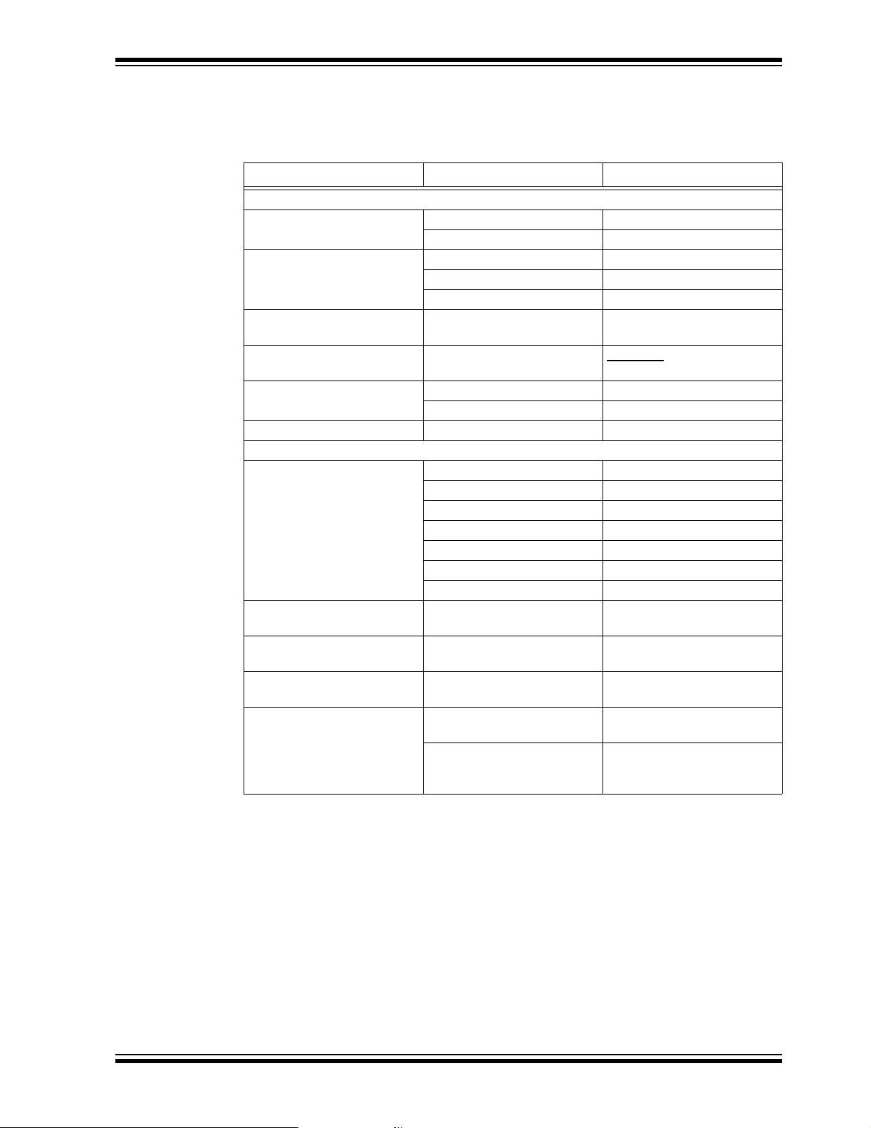
CONVENTIONS USED IN THIS GUIDE
This manual uses the following documentation conventions:
DOCUMENTATION CONVENTIONS
Description Represents Examples
Arial font:
Italic characters Referenced books
Initial caps A window the Output window
Quotes A field name in a window or
Underlined, italic text with
right angle bracket
Bold characters A dialog button Click OK
Text in angle brackets < > A key on the keyboard Press <Enter>, <F1>
Courier New font:
Plain Courier New Sample source code #define START
Italic Courier New A variable argument file.o, where file can be
Square brackets [ ] Optional arguments mcc18 [options] file
Curly brackets and pipe
character: { | }
Ellipses... Replaces repeated text var_name [,
Preface
MPLAB® IDE User’s Guide
Emphasized text ...is the
A dialog the Settings dialog
A menu selection select Enable Programmer
“Save project before build”
dialog
A menu path
A tab Click the Power tab
Filenames autoexec.bat
File paths c:\mcc18\h
Keywords _asm, _endasm, static
Command-line options -Opa+, -Opa-
Bit values 0, 1
Constants (in source code) 0xFF, ‘A’
Choice of mutually exclusive
arguments; an OR selection
Represents code supplied by
user
File>Save
any valid filename
[options]
errorlevel {0|1}
var_name...]
void main (void)
{ ...
}
only
compiler...
WARRANTY REGISTRATION
Please complete the enclosed Warranty Registration Card and mail it promptly.
Sending in the Warranty Registration Card entitles users to receive new product
updates. Interim software releases are available at the Microchip web site.
© 2005 Microchip Technology Inc. DS51589A-page 2
Page 7

Explorer 16 Development Board User’s Guide
RECOMMENDED READING
This user’s guide describes how to use the Explorer 16 Development Board. Other
useful documents are listed below. The following Microchip documents are available
and recommended as supplemental reference resources.
Readme for the Explorer 16 Development Board
For the latest information on using the Explorer 16 Development Board, read the
Readme for Explorer 16 Development Board.txt file (an ASCII text file) at
the root level of the Explorer 16 CD-ROM. The Readme file contains update information
and known issues that may not be included in this user’s guide.
Readme Files
For the latest information on using other tools, read the tool-specific Readme files in
the Readmes subdirectory of the MPLAB IDE installation directory. The Readme files
contain update information and known issues that may not be included in this user’s
guide.
PIC24FJ128GA010 PS Data Sheet (DS39756) and PIC24FJ128GA Family
Data Sheet (DS39747)
Consult this document for detailed information on the PIC24F general purpose, 16-bit
devices. Reference information found in this data sheet includes:
• Device memory map
• Device pinout and packaging details
• Device electrical specifications
• List of peripherals included on the device
Note that document, DS39756, is for use only with the initial prototype samples of the
PIC24F family. These devices are all marked with a “PS” suffix at the end of the device
number. For all other PIC24FJ128GA family devices, including those with an “ES”
suffix, use DS39747.
dsPIC33F Family Data Sheet (DS70165)
Consult this document for detailed information on the dsPIC33F Digital Signal
Controllers. Reference information found in this data sheet includes:
• Device memory map
• Device pinout and packaging details
• Device electrical specifications
• List of peripherals included on the device
dsPIC30F Programmer’s Reference Manual (DS70030)
This manual is a software developer’s reference for all of Microchip’s 16-bit digital
signal controllers. It describes the instruction set in detail and also provides general
information to assist in developing software for PIC24 MCUs, dsPIC30F and dsPIC33F
DSCs.
PIC24H Family Overview (DS70166)
This document provides an overview of the functionality of the new PIC24H product
family. It helps determine how the PIC24H high-performance, 16-bit microcontrollers fit
a specific product application.
DS51589A-page 3 © 2005 Microchip Technology Inc.
Page 8

MPLAB® C30 C Compiler User’s Guide (DS51284)
This document details the use of Microchip’s MPLAB C30 C Compiler for dsPIC
devices to develop an application. MPLAB C30 is a GNU-based language tool, based
on source code from the Free Software Foundation (FSF). For more information about
the FSF, see www.fsf.org.
Other GNU language tools available from Microchip are:
• MPLAB ASM30 Assembler
• MPLAB LINK30 Linker
• MPLAB LIB30 Librarian/Archiver
MPLAB
Consult this document for more information pertaining to the installation and
implementation of the MPLAB Integrated Development Environment (IDE) software.
®
IDE Simulator, Editor User’s Guide (DS51025)
THE MICROCHIP WEB SITE
Microchip provides online support via our web site at www.microchip.com. This web
site is used as a means to make files and information easily available to customers.
Accessible by using your favorite Internet browser, the web site contains the following
information:
• Product Support – Data sheets and errata, application notes and sample
programs, design resources, user’s guides and hardware support documents,
latest software releases and archived software
• General Technical Support – Frequently Asked Questions (FAQs), technical
support requests, online discussion groups, Microchip consultant program
member listing
• Business of Microchip – Product selector and ordering guides, latest Microchip
press releases, listing of seminars and events, listings of Microchip sales offices,
distributors and factory representatives
Preface
®
© 2005 Microchip Technology Inc. DS51589A-page 4
Page 9

Explorer 16 Development Board User’s Guide
DEVELOPMENT SYSTEMS CUSTOMER CHANGE NOTIFICATION SERVICE
Microchip’s customer notification service helps keep customers current on Microchip
products. Subscribers will receive e-mail notification whenever there are changes,
updates, revisions or errata related to a specified product family or development tool of
interest.
To register, access the Microchip web site at www.microchip.com, click on Customer
Change Notification and follow the registration instructions.
The Development Systems product group categories are:
• Compilers – The latest information on Microchip C compilers and other language
tools. These include the MPLAB C18 and MPLAB C30 C compilers; MPASM™
and MPLAB ASM30 assemblers; MPLINK™ and MPLAB LINK30 object linkers;
and MPLIB™ and MPLAB LIB30 object librarians.
• Emulators – The latest information on Microchip in-circuit emulators.This
includes the MPLAB ICE 2000 and MPLAB ICE 4000.
• In-Circuit Debuggers – The latest information on the Microchip in-circuit
debugger, MPLAB ICD 2.
• MPLAB
Integrated Development Environment for development systems tools. This list is
focused on the MPLAB IDE, MPLAB SIM simulator, MPLAB IDE Project Manager
and general editing and debugging features.
• Programmers – The latest information on Microchip programmers. These
include the MPLAB PM3 and PRO MATE
PICSTART
®
IDE – The latest information on Microchip MPLAB IDE, the Windows®
®
®
Plus and PICkit™ 1 development programmers.
II device programmers and the
CUSTOMER SUPPORT
Users of Microchip products can receive assistance through several channels:
• Distributor or Representative
• Local Sales Office
• Field Application Engineer (FAE)
• Technical Support
• Development Systems Information Line
Customers should contact their distributor, representative or field application engineer
(FAE) for support. Local sales offices are also available to help customers. A listing of
sales offices and locations is included in the back of this document.
Technical support is available through the web site at: http://support.microchip.com
DOCUMENT REVISION HISTORY
Revision A (November 2005)
This is the initial release of this Document.
DS51589A-page 5 © 2005 Microchip Technology Inc.
Page 10

NOTES:
Preface
© 2005 Microchip Technology Inc. DS51589A-page 6
Page 11

EXPLORER 16 DEVELOPMENT
BOARD USER’S GUIDE
Chapter 1. Intr od ucin g the Explorer 16 Development Board
1.1 INTRODUCTION
Thank you for purchasing Microchip Technology’s Explorer 16 Development Board Kit.
The development board provides a low-cost, modular development system for
Microchip’s new line of 16-bit microcontroller families, including the PIC24, PIC24H and
the 16-bit digital signal controller family, dsPIC33F.
As provided, the development board works as a demo board right from the box, and
also has the ability to extend its functionality through modular expansion interfaces.
The Explorer 16 board supports MPLAB ICD 2 for full emulation and debug capabilities,
and also allows 3V controllers to interface with 5V peripheral devices.
1.2 HIGHLIGHTS
This chapter covers the following topics:
• What’s in the Kit
• Explorer 16 Development Board Functionality and Features
• Using the Explorer 16 Out of the Box
• Explorer 16 Development Board Demonstration Programs
• Reference Documents
1.3 WHAT’S IN THE KIT
The Explorer 16 Development Board Kit contains the following:
• The Explorer 16 Development Board.
• A preprogrammed PIC24FJ128GA010 Processor Installation Module (PIM),
already installed to the board
• A preprogrammed dsPIC33FJ256GP710 PIM
• An RS-232 cable
• The Explorer 16 Development CD ROM, containing:
- This User’s Guide
- Data Sheets for the PIC24FJ128GA family and dsPIC33FJ256GP family
- Schematics and PCB drawing files for the PIM modules
- Example programs for use with the PIC24 and dsPIC33F devices
- Files detailing general purpose expansion boards that can be used with the
Explorer 16 board (provided in Gerber format)
If you are missing any part of the kit, please contact your nearest Microchip sales office,
listed on the last page of this manual, for further assistance.
Note: The Explorer 16 Development Board has been designed to function prima-
rily from a permanently mounted PIC24FJ128GA010 device at position U1.
Initial units will be shipped with U1 unpopulated and a PIC24FJ PIM of
equal functionality mounted on the U1A headers instead. When using the
PIC24FJ PIM or any other PIM, it is critical to verify that switch S2 always
remains in the “PIM” position. See Section 4.2.1 “Processor Support” for
more information.
© 2005 Microchip Technology Inc. DS51589A-page 7
Page 12

Introducing the Explorer 16 Development Board
1.4 EXPLORER 16 DEVELOPMENT BOARD FUNCTIONALITY AND FEATURES
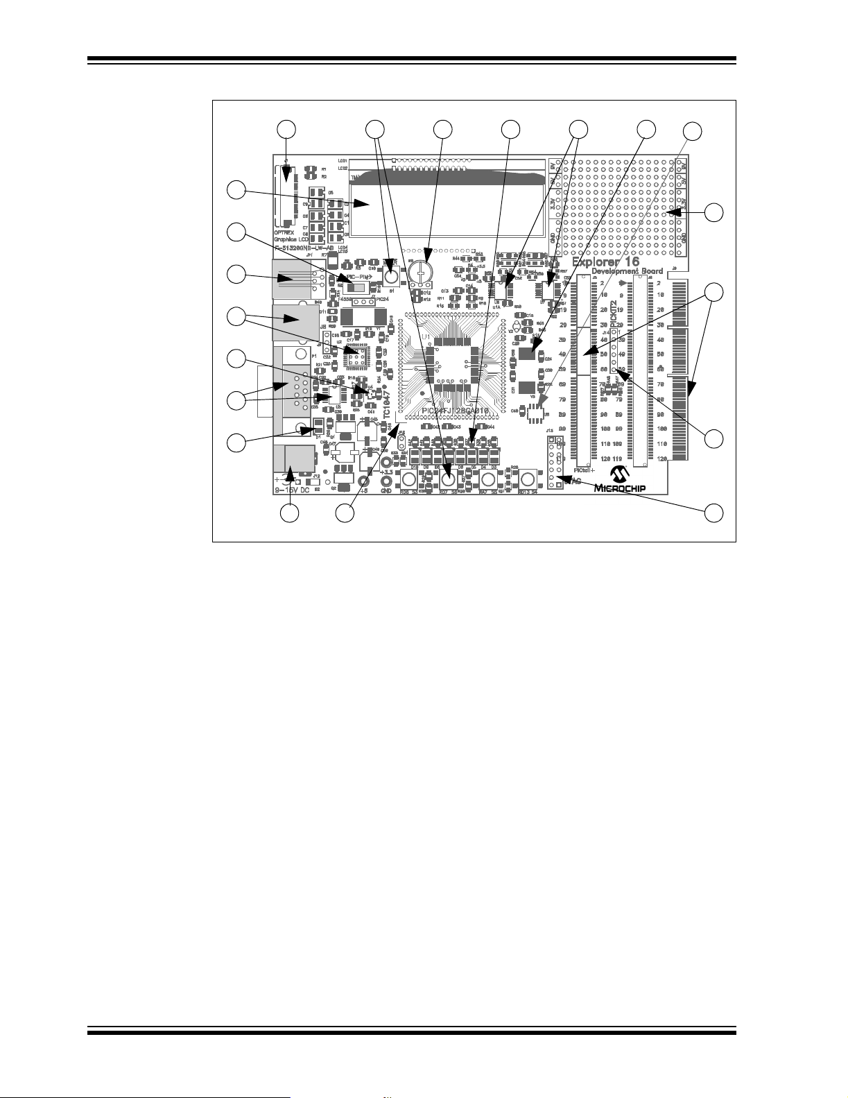
A layout of the Explorer 16 Development Board is shown in Figure 1-1. The board
includes these key features, as indicated in the diagram:
1. 100-pin PIM riser, compatible with the PIM versions of all Microchip
PIC24F/24H/dsPIC33F devices
2. Direct 9 VDC power input that provides +3.3V and +5V (regulated) to the entire
board
3. Power indicator LED
4. RS-232 serial port and associated hardware
5. On-board analog thermal sensor
6. USB connectivity for communications and device programming/debugging
7. Standard 6-wire In-Circuit Debugger (ICD) connector for connections to an
MPLAB ICD 2 programmer/debugger module
8. Hardware selection of PIM or soldered on-board microcontroller
(in future versions)
9. 2-line by 16-character LCD
10. Provisioning on PCB for add on graphic LCD
11. Push button switches for device Reset and user-defined inputs
12. Potentiometer for analog input
13. Eight indicator LEDs
14. 74HCT4053 multiplexers for selectable crossover configuration on serial com-
munication lines
15. Serial EEPROM
16. Independent crystals for precision microcontroller clocking (8 MHz) and RTCC
operation (32.768 kHz)
17. Prototype area for developing custom applications
18. Socket and edge connector for PICtail™ Plus card compatibility
19. Six-pin interface for PICkit 2 Programmer
20. JTAG connector pad for optional boundary scan functionality
For additional details on these features, refer to Chapter 4. “Explorer 16 Development
Hardware”.
1.4.1 Sample Devices Included with the Development Kit
Each Explorer 16 Development Board Kit contains two preprogrammed 16-bit devices:
a PIC24FJ128GA010 and a dsPIC33FJ256GP710. These are provided as 100-pin
PIMs on riser sockets, which can be quickly installed on pin header U1A and
exchanged as needed.
Note: As Microchip’s 16-bit portfolio develops, alternate devices may be included
with the Explorer 16 Development Board Kit. It is anticipated that one
device each of the PIC24 and dsPIC33F families will always be included.
Also in the future, the included PIC24 device will be soldered onto the board
and only the dsPIC33F device will be provided as a PIM.
© 2005 Microchip Technology Inc. DS51589A-page 8
Page 13
Explorer 16 Development Board User’s Guide
FIGURE 1-1: EXPLORER 16 DEVELOPMENT BOARD LAYOUT
10
9
8
7
6
5
4
3
2
11 1412 13 15
1
16
17
18
19
20
1.5 USING THE EXPLORER 16 OUT OF THE BOX
Although intended as a development platform, the Explorer 16 board may also be used
directly from the box as a demonstration board for PIC24 and dsPIC33F devices. The
programs discussed in Chapter 3. “Explorer 16 Tutorial Programs” are
preprogrammed into the sample device PIMs (i.e., PIC24ExplDemo.hex for the
PIC24 device and dsPIC33ExplDemo.hex for the dsPIC33F device) and are ready
for immediate use.
To get started with the board:
1. For Explorer 16 boards without a permanently mounted PIC24FJ device: verify
that the PIC24FJ128GA010 PIM is correctly installed onto the board. If you want
to use the dsPIC
dsPIC33F PIM in its place. For all PIMs, be certain to align the PIM so the
notched corner marking is oriented in the upper left corner.
2. For Explorer 16 boards without a permanently mounted PIC24FJ device: verify
that switch S2 is set in the “PIM” position.
For Explorer 16 boards with a permanently mounted PIC24FJ device: verify that
switch S2 is set in the “PIC” position.
3. Verify that the jumper on JP2 is installed (to enable the LEDs).
4. Apply power to the board (9 VDC) at power input J2. For information on acceptable power sources, see Appendix A. “Explorer 16 Development Board
Schematics”.
Refer to Chapter 3. “Explorer 16 Tutorial Programs” for details on the demonstration
code operation.
®
device PIM, carefully remove the PIC24 PIM and install the
DS51589A-page 9 © 2005 Microchip Technology Inc.
Page 14
Introducing the Explorer 16 Development Board
FIGURE 1-2: EXPLORER 16 PIM MODULE, SHOWING NOTCHED CORNER
MARKING
PIC24FJ128GA010
1.6 EXPLORER 16 DEVELOPMENT BOARD DEMONSTRATION PROGRAMS
The preprogrammed example code on the PIMs has been included on the Explorer 16
CD-ROM for future reference. All project files have been included, so that the code may
be used directly to restore a PIM to its original state (i.e., if the sample device has been
reprogrammed with another program), or so the user may use the tutorial code as a
platform for further experimentation.
In addition, the CD-ROM contains sample demonstration programs for both PIC24 and
dsPIC33F family devices. Separate demo source code (as files in C) and compiled
code files (in Hex) are provided for each family. These may be used with the included
PIC24 and dsPIC33F PIMs by reprogramming the devices using MPLAB ICD 2.
1.7 REFERENCE DOCUMENTS
In addition to the documents listed in the “Recommended Reading” section, these
documents are also available from Microchip to support the use of the Explorer 16
Development Board:
PIC18F2455/2550/4455/4550 Data Sheet
•
TC1047/TC1047A Data Sheet
•
•
25AA256/25LC256 Data Sheet
•
PICkit™ 2 Microcontroller Programmer User’s Guide
MPLAB® ICD 2 In-Circuit Debugger Quick Start Guide
•
•
PRO MATE® II User’s Guide
You can obtain these reference documents from your nearest Microchip sales office
(listed in the back of this document) or by downloading them from the Microchip web
site (www.microchip.com).
(DS39632)
(DS21498)
(DS21822)
(DS51553)
(DS51268)
(DS30082)
© 2005 Microchip Technology Inc. DS51589A-page 10
Page 15

Chapter 2. Explorer 16 Programming Tutorial
2.1 INTRODUCTION
This chapter is a self-paced tutorial to get you started using the Explorer 16 Development
Board.
2.2 HIGHLIGHTS
Items discussed in this chapter include:
• Tutorial Overview
• Creating the Project
• Building the Code
• Programming the Device
2.3 TUTORIAL OVERVIEW
The tutorial in this chapter demonstrates the main features of the MPLAB IDE and
MPLAB ICD 2 as they are used with the Explorer 16 Development Board. As presented, it is designed for use with the PIC24FJ128GA010 specifically. However, the
same procedures and toolsuites can also be used with PIC24H or dsPIC33F devices.
The PIC24 tutorial project demonstrated here, PIC24ExplDemo.mcp, is written in C
for MPLAB C30. The program displays PIC24 features on the alphanumeric LCD, and
also displays voltage, temperature and date/time as the various buttons are pressed.
Described with the PIC24 project is the dsPIC device tutorial,
Example1_RTC_LED_ADC.mcp. It is also written in C for MPLAB C30. The program
displays voltage and current time, updating the display on command. Both programs
are described in more detail in Chapter 3. “Explorer 16 Tutorial Programs”.
For either project, the source file (PIC24ExplDemo.c or main_rtc.c for PIC24 or
dsPIC33F, respectively) is used with a linker script file (p24fj128ga010.gld or
p33fj256gp710ps.gld) and header file (p24fj128ga010.h or
p33fj256gp710ps.h) to form a complete project. While these simple projects use a
single source code file, more complex projects might use multiple assembler and
compiler source files, as well as library files and precompiled object files.
Upon completing this tutorial, you should be able to:
• Create a project using the Project Wizard
• Assemble and link the code and set the Configuration bits
• Set up MPLAB IDE to use the MPLAB ICD 2
• Program the chip with the MPLAB ICD 2
There are three steps to this tutorial:
1. Creating a project in MPLAB IDE.
2. Assembling and linking the code.
3. Programming the chip with the MPLAB ICD 2.
EXPLORER 16 DEVELOPMENT
BOARD USER’S GUIDE
© 2005 Microchip Technology Inc. DS51589A-page 11
Page 16
2.4 CREATING THE PROJECT
The first step is to create a project and a workspace in MPLAB IDE. Typically, there is
one project in one workspace.
Note: These instructions presume the use of MPLAB IDE 7.22 or newer.
A project contains the files needed to build an application (source code, linker script
files, etc.) along with their associations to various build tools and build options.
A workspace contains one or more projects and information on the selected device,
debug tool and/or programmer, open windows and their location and other MPLAB IDE
configuration settings.
MPLAB IDE contains a Project Wizard to help create new projects. Before starting,
create a folder named Tutorial for the project files for this tutorial (C:\Tutorial is
assumed in the instructions that follow). From the Example Code\Tutorial Code
directory on the Explorer 16 Development Kit Software CD-ROM, copy all of the source
files into this folder.
Note: The screen shots in the following sections show the PIC24 tutorial. Except for
displayed file names, the screens for the dsPIC33F tutorial will be identical.
2.4.1 Select a Device
Explorer 16 Programming Tutorial
1. Start MPLAB IDE.
2. Close any workspace that might be open (
3. From the
4. From the Welcome screen, click Next > to display the Project Wizard Step One
dialog (Figure 2-1).
FIGURE 2-1: SELECTING THE DEVICE
Project
menu, select
Project Wizard.
File > Close Workspace
).
5. From the Device drop-down list, select “PIC24FJ128GA010” or
“dsPIC33FJ256GP710PS”, depending on the PIM being used. Click Next >. The
Project Wizard Step Two dialog will be displayed (see Figure 2-2).
© 2005 Microchip Technology Inc. DS51589A-page 12
Page 17
Explorer 16 Development Board User’s Guide
FIGURE 2-2: SELECTING THE TOOLSUITE
2.4.2 Select Language Toolsuite
1. From the Active Toolsuite drop-down list, select Microchip C30 Toolsuite. This
toolsuite includes the assembler and linker that will be used.
2. In the Toolsuite Contents combo box, select MPLAB C30 Compiler
(pic30-gcc.exe).
3. In the Location box, click Browse... and navigate to
C:\Program Files\Microchip\MPLAB C30\bin\pic30-as.exe.
4. With MPLAB LINK 30 Object Linker (pic30-ld.exe) selected in Toolsuite
Contents, click Browse... and navigate to
C:\Program Files\Microchip\MPLAB C30\bin\pic30-Id.exe.
5. Click Next > to continue. The Project Wizard Step Three dialog displays
(Figure 2-3).
DS51589A-page 13 © 2005 Microchip Technology Inc.
Page 18
Explorer 16 Programming Tutorial
FIGURE 2-3: NAMING YOUR PROJECT
2.4.3 Name Your Project
1. In the Project Name text box, type “MyProject”.
2. In the Project Directory box, click Browse... and navigate to C:\Tutorial to
place your project in the Tutorial folder.
3. Click Next > to continue. The Project Wizard Step Four dialog displays
(Figure 2-4).
FIGURE 2-4: ADDING FILES TO THE PROJECT
© 2005 Microchip Technology Inc. DS51589A-page 14
Page 19

Explorer 16 Development Board User’s Guide
2.4.4 Add Files to Project
1. From the list of folders on the PC, locate the C:\Tutorial folder.
2. Select the source (.c) and header (.h) files. Click Add >> to include the file in
the project.
3. Expand the C:\Program Files\Microchip\MPLAB 30\support\gld
folder and select the p24fj128ga010.gld or p33fj256gp710ps.gld file,
as appropriate.
4. Click Add >> to include this file in the project. There should now be two files in
the project.
5. Click Next > to continue.
6. When the summary screen displays, click Finish.
After the Project Wizard completes, the MPLAB Project window shows the source files
in the Source Files folder and the appropriate linker script in the Linker Scripts folder
(Figure 2-5).
FIGURE 2-5: PROJECT WINDOW
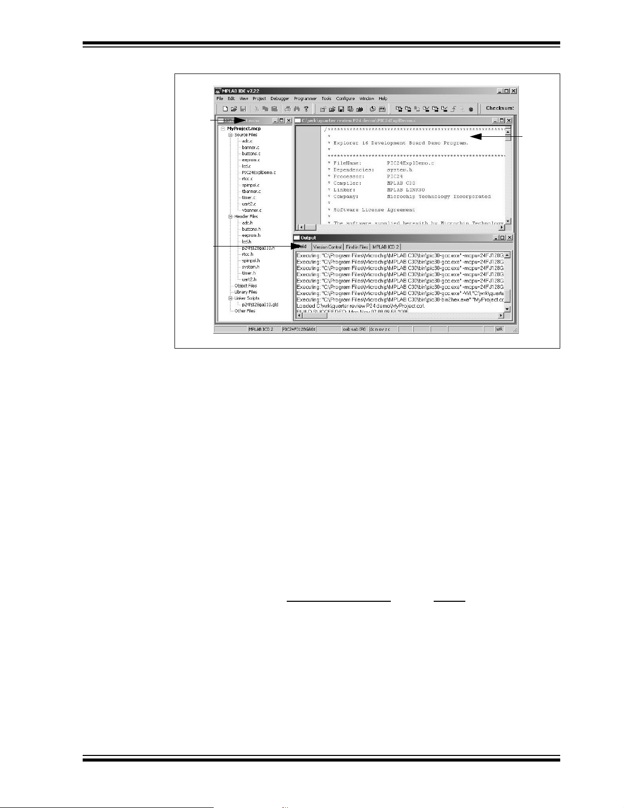
A project and workspace has now been created in MPLAB IDE. MyProject.mcw is
the workspace file and MyProject.mcp is the project file. Double-click the
PIC24ExplDemo.c file (for PIC24) or main_rtc.c file (for dsPIC33F) in the Project
window to open the file. MPLAB IDE should now look similar to Figure 2-6.
DS51589A-page 15 © 2005 Microchip Technology Inc.
Page 20
Explorer 16 Programming Tutorial
FIGURE 2-6: MPLAB® IDE WORKSPACE
Project
Window
Output
Window
Source
Code
Window
2.5 BUILDING THE CODE
In this project, building the code consists of compiling the source files to create an
object file, MyProject.o, then linking the object file to create the MyProject.hex
and MyProject.cof output files. (For dsPIC33F projects, the files would be
Example1_RTC_LED_ADC.o, Example1_RTC_LED_ADC.hex and
Example1_RTC_LED_ADC.cof.)The Hex file contains the data necessary to program
the device, and the .cof file contains additional information that lets you debug the
code at the source code level.
Before building, there are settings required to tell MPLAB IDE where to find the include
files and to reserve space for the extra debug code when the MPLAB ICD 2 is used.
For PIC24 projects, the following line in the system.h file is:
#include “p24fj128ga010.h”
For dsPIC33 projects, the line is:
#include “p33fj256gp710ps.h”
This line causes a standard include file to be used. Microchip provides these files with
all the Special Function Register (SFR) labels already defined for convenience.
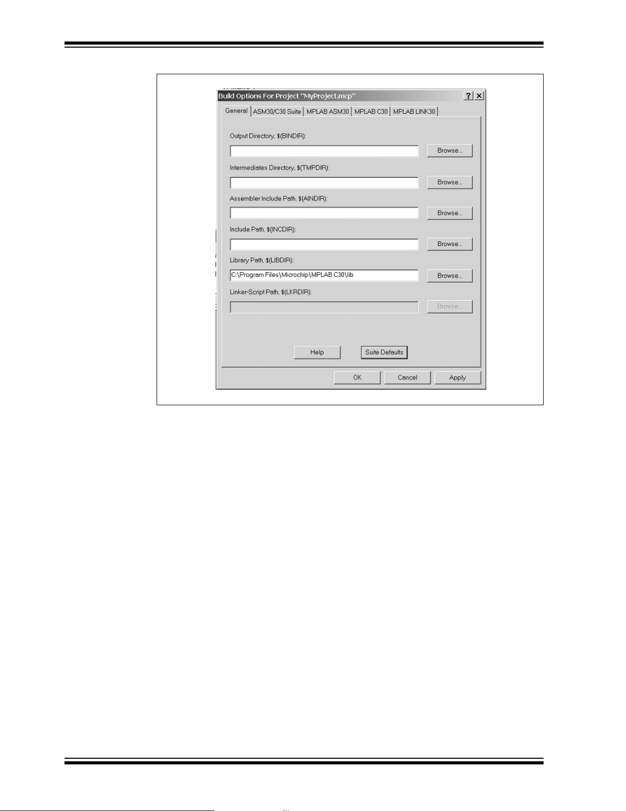
To build the code, select
Options dialog displays (Figure 2-7).
Build Options > Project
from the
Project
menu. The Build
© 2005 Microchip Technology Inc. DS51589A-page 16
Page 21
Explorer 16 Development Board User’s Guide
FIGURE 2-7: BUILD OPTIONS
2.5.1 Identify Assembler Include Path
1. Select the General tab.
2. Click Suite Default. This tells the environment where to find the library files.
3. Select the MPLAB LINK30 tab to view the linker settings (Figure 2-8).
4. Check Link for ICD2.
5. Click OK. The text box closes while the linker reserves space for the debug code
used by the MPLAB ICD 2.
6. Click OK again to save these changes. The project is now ready to build.
DS51589A-page 17 © 2005 Microchip Technology Inc.
Page 22

Explorer 16 Programming Tutorial
FIGURE 2-8: MPLAB® LINK30 BUILD OPTIONS
2.5.2 Build the Project
From the menu bar of the main MPLAB IDE window, select
Output window displays (Figure 2-9).
Observe the progress of the build. When the “BUILD SUCCEEDED” message displays,
you are ready to program the device.
FIGURE 2-9: BUILD OUTPUT
Project
>
Make
. The Build
© 2005 Microchip Technology Inc. DS51589A-page 18
Page 23

Explorer 16 Development Board User’s Guide
2.6 PROGRAMMING THE DEVICE
The MPLAB ICD 2 In-Circuit Debugger is used to program and debug the
microcontroller in-circuit on the Explorer 16 Development Board.
Note: Before proceeding, make sure that the USB driver for the MPLAB ICD 2 has
been installed on the PC (see the
User’s Guide
MPLAB ICD 2).
(DS51331) for more details regarding the installation of the
2.6.1 Set Up the Device Configuration
The device configuration for the target microcontroller can be set by two methods:
using configuration macros in the source code, or using the Configuration Bits window
in MPLAB IDE.
The PIC24 Explorer 16 tutorial code already includes configuration macros in the
source code itself. It is only necessary to confirm that the following macros are in place
near the top of the PIC24ExplDemo.c file:
_CONFIG1(JTAGEN_OFF & GSS0_OFF & GWRP_OFF & BKBUG_OFF & COE_OFF
& FWDTEN_OFF & FNOSC_PRI)
_CONFIG2(FCKSM_CSDCMD & OSCIOFNC_ON & POSCMOD_HS)
For the dsPIC33F tutorial code, confirm that the following macros are in place near the
top of the main_rtc.c file:
_FGS(CODE_WRITE_PROT_OFF);
_FOSCSEL(FRC_PLL);
_FOSC(CSW_FSCM_OFF & OSC2_IO & XT);
_FWDT(WDT_OFF);
If configuration macros are not used in the source code, it is also possible to set device
configuration with the Configuration Bits window. For the PIC24 code, the process is as
follows:
1. From the main window’s menu bar, select
display the configuration settings (Figure 2-10).
2. Set the Configuration bits by clicking on a particular line item and selecting an
option from the drop-down menu that appears. The Configuration bits should be
set as shown in Figure 2-10.
The settings that will most likely need to change are:
a) Primary Oscillator Select: HS Oscillator Enabled
b) Oscillator Select: Primary Oscillator (XT, HS, ES)
c) Clock Switching and Monitor: SW Disabled, Mon Disabled
d) Watchdog Timer Enable: Disable
MPLAB® ICD 2 In-Circuit Debugger
Configure > Configuration Bits
to
DS51589A-page 19 © 2005 Microchip Technology Inc.
Page 24

Explorer 16 Programming Tutorial
FIGURE 2-10: CONFIGURATION SETTINGS (PIC24)
Note: Do not use the Configuration Bits window to set device configuration if
configuration macros are already used in the source code. In cases where
both methods are used, configuration macros may override settings from
the Configuration Bits window. Refer to the
User’s Guide
(DS51025) for additional information.
2.6.2 Connect and Enable MPLAB ICD 2
1. Connect the MPLAB ICD 2 module to the PC with the USB cable.
2. Connect the MPLAB ICD 2 to the Explorer 16 Development Board with the short
RJ-11 cable.
3. Apply power to the Explorer 16 board.
4. From the
ICD 2 as the debug tool in MPLAB IDE.
5. From the
MPLAB IDE should report that it found the PIC24FJ128GA010 device, as shown
in Figure 2-11.
Debugger
Debugger
menu, click
menu, select
Select Tool > MPLAB ICD 2
Connect
to connect the debugger to the device.
MPLAB IDE Simulator, Editor
to set the MPLAB
Note: MPLAB IDE may need to download new firmware if this is the first time the
MPLAB ICD 2 is being used with a PIC24FJ device. Allow it to do so. If any
errors are shown, double-click the error message to get more information.
FIGURE 2-11: ENABLING MPLAB
®
ICD 2
Status indicates
device is found
© 2005 Microchip Technology Inc. DS51589A-page 20
Page 25

Explorer 16 Development Board User’s Guide
2.6.3 Program the Device
1. From the
window (Figure 2-12) displays the program steps as they occur.
2. Observe the results of the programming. When “MPLAB ICD 2 Ready” displays,
the device is programmed and ready to run.
FIGURE 2-12: PROGRAMMING THE DEVICE
Debugger
menu, select
Program
to program the part. The Output
DS51589A-page 21 © 2005 Microchip Technology Inc.
Page 26

NOTES:
Explorer 16 Programming Tutorial
© 2005 Microchip Technology Inc. DS51589A-page 22
Page 27

EXPLORER 16 DEVELOPMENT
Chapter 3. Explorer 16 Tutorial Programs
3.1 INTRODUCTION
This chapter provides a high-level overview of the PIC24 and dsPIC33F firmware
programmed during the tutorial exercise in the previous chapter.
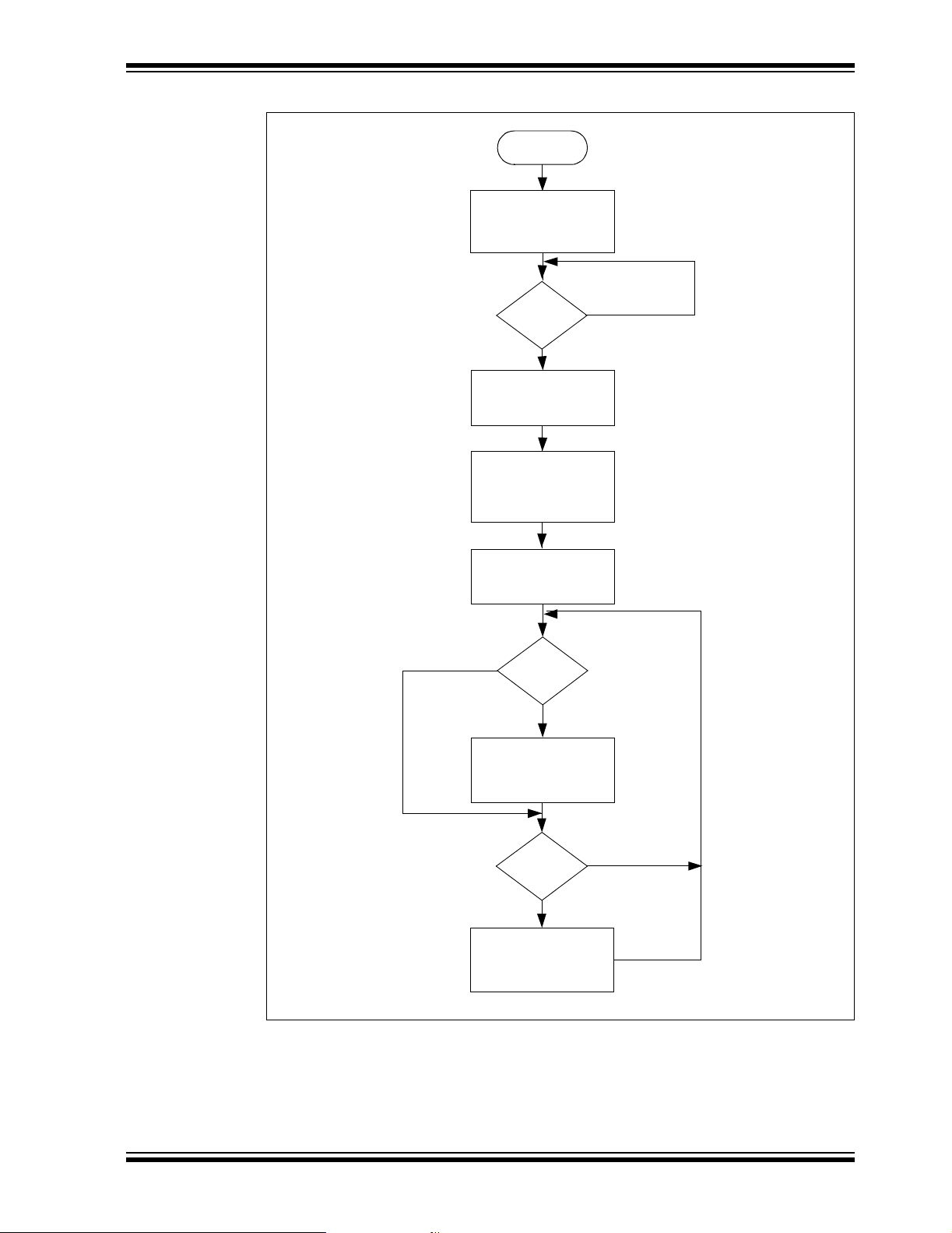
3.2 PIC24 TUTORIAL PROGRAM OPERATION
The PIC24 tutorial program is made up of three components which are individually
displayed on the LCD. The program is used to demonstrate the new Parallel Master
Port (PMP) module which is used to drive the LCD, as well as the new Real-Time
Clock/Calendar module (RTCC). The program flow is shown in Figure 3-1.
3.2.1 PIC24 Features
Features mode displays a continuous description of the PIC24FJ128GA010 device
feature set. To exit the display and continue to the next mode, press S4.
3.2.2 Voltmeter/Temperature
BOARD USER’S GUIDE
Voltmeter/Temperature mode uses the code modules, vbanner.c and ADC.c, and
the A/D module to measure analog signals from the board and convert them for display
on the LCD. The voltage is taken from the potentiometer (R6) and displays a voltage
between 0.00V and 3.29V on line 1 of the LCD. Temperature is from a TC1074A analog
thermal sensor (U5). The temperature is displayed on line 2 of the LCD and automatically alternates between Celsius and Fahrenheit values. The voltage and
temperature are updated continuously.
This mode also lets users store the current temperature in the on-board serial
EEPROM by pressing S5. Pressing S6 switches the display between current and
stored temperature values. An ‘M’ on the right side of the LCD indicates that a stored
temperature value is being displayed.
To exit and continue to the next mode, press S4.
3.2.3 Clock/Calendar
Clock/Calendar mode uses code in the modules, rtcc.c and tbanner.c. Once this
mode is entered from the main menu, a Real-Time Clock will start counting from
10:00:00, and display the date and day for Oct. 10, 2005. The new RTCC module and
a 32 kHz clock crystal are used to provide the Real-Time Clock with day/date calendar.
In Clock/Calendar mode, the user-defined push buttons do the following:
• S3 toggles the Clock Set mode, which allows the user to set the date and time.
Setup mode starts with the tens digit of the hour in the time display.
• S4 accepts the value of the current item and moves cursor to the next item.
• S5 decrements the currently selected item.
• S6 increments the currently selected item.
Pressing S3 once superimposes a flashing cursor over the tens digit of the hour in the
time display. Each press of S4 moves the cursor sequentially through the digits of the
time display, then the month, day and year. Pressing S3 at any time in the process
returns to the regular clock/calendar display.
© 2005 Microchip Technology Inc. DS51589A-page 23
Page 28

Explorer 16 Tutorial Programs
Pressing S4 at this point exits Clock/Calendar mode and returns the device to the
PIC24 Features mode.
The data that is sent to the LCD is also sent to the RS-232 serial port using the UART.
A terminal emulator, such as HyperTerminal (installed by default on most Microsoft
Windows systems), will be able to display the same information. To do this, set the
terminal emulator for 19200 baud, 8-bit data, 1 Stop bit and no parity check.
FIGURE 3-1: PIC24 TUTORIAL PROGRAM FLOWCHART
Power-up
Display
“Explorer 16
Development Board”
Display
PIC24 Features
Scrolling Banner
®
Yes
Is S4
pressed?
No
No
Is S4
pressed?
Display Voltage
and Temperature
Is S4
pressed?
Display
“Mon 10:00:00”
“Oct 10, 2005”
Yes
Yes
No
pressed?
Store Temperature
in EEROM
Is S5
Yes
No
Toggle Displayed
Temperature between
Current and Stored
Is S6
pressed?
Yes
No
Is S3
pressed?
Yes
Clock Setup mode:
S3 – Exit Setup mode
S4 – Accept Selection, Adjust Next Value
S5 – Decrement Selection
S6 – Increment Selection
© 2005 Microchip Technology Inc. DS51589A-page 24
No
Page 29

Explorer 16 Development Board User’s Guide
3.3 dsPIC33F TUTORIAL PROGRAM OPERATION
The dsPIC33F tutorial program is made up of five simple processes which continuously
execute on the dsPIC33FJ256GP710 device:
• Real-Time Clock (RTC) using Timer1
• A/D conversion of Potentiometer (R6)
• A/D volts to Hex conversion
• Hex to Decimal conversion (for LCD display)
• LCD Update
The time of day and A/D conversion values are continually updated and displayed on
the LCD. The program demonstrates the basic code to initialize Timer1, enable the
Timer1 oscillator for RTC operation, and initialize the A/D for single channel conversion
of potentiometer, RP5. The LCD is driven via the port pins. The program flow is shown
in Figure 3-2.
In addition to the tutorial, the Explorer 16 CD also provides code examples to demonstrate higher level processing requirements, such as DMA, digital filters and Fast
Fourier Transforms (FFT). See Code Example 2 on the CD for more information.
3.3.1 Voltmeter
The simple tutorial program initializes the A/D module for 12-bit mode with
auto-sampling and conversion of the potentiometer connected to pin AN5 and initializes the respective interrupt. The A/D module continually samples and converts the
potentiometer signal (0 to 3.3 VDC) on analog channel, AN5. When a conversion is
complete, an interrupt is generated and the result in the ADCBUF0 register is copied
into a temporary variable, temp1. The adc_lcd_update flag is then asserted and the
A/D Interrupt Flag, AD1IF (IFS0<13>), is cleared.
The program exits the Interrupt Service Routine and re-enters the main program loop.
The variable, adc_lcd_update
a new A/D conversion value which can be converted and displayed on the LCD.
The primary code modules associated with the operation of the ADC module and
display are:
• init_ADC.c
• isr_ADC.c
• advolts.c
• hexdec.c
,
is evaluated in the main loop to determine if there is
3.3.2 Real-Time Clock
The tutorial program also supports a Real-Time Clock demo. Timer1 is initialized with
interrupts enabled and the external 32.768 kHz oscillator is enabled. Within the Timer1
Interrupt Service Routine (once every second), the variables, hours, minutes and
seconds, are updated, the flag variable, rtc_lcd_update, is asserted and the
Timer1 Interrupt Flag, T1IF (IFS0<3>), is cleared.
The program exits the Interrupt Service Routine and re-enters the main program loop.
The variable, rtc_lcd_update, is evaluated in the main loop to determine if there is
a new time of day value which can be converted and displayed on the LCD.
The primary code modules associated with the operation of the Timer1 module and
display are:
• init_timer1.c
• isr_timer1.c
• hexdec.c
DS51589A-page 25 © 2005 Microchip Technology Inc.
Page 30
Explorer 16 Tutorial Programs
FIGURE 3-2: dsPIC33F TUTORIAL PROGRAM FLOWCHART
Power-up
Display
“dsPIC33 Demo”
“Press S3 to cont”
Is S3
pressed?
Initialize Timer1
Display
“Time 00:00:00”
“R6 = 0.00 VDC”
Initialize A/D Converter
No
Update
time?
Convert Time of Day
to Decimal and
Call Update_LCD
No
Yes
Yes
Update
volts?
Convert A/D Result
to Decimal and
Call Update_LCD
© 2005 Microchip Technology Inc. DS51589A-page 26
No
Yes
Page 31
Chapter 4. Explorer 16 Development Hardware
4.1 INTRODUCTION
This chapter provides a more detailed description of the hardware features of the
Explorer 16 Development Board.
4.2 HARDWARE FEATURES
The key features of the Explorer 16 board are listed below. They are presented in the order
given in
Figure 1-1.
4.2.1 Processor Support
The Explorer 16 board has been designed to accommodate both permanently mounted
(i.e., soldered on) and detachable PIM processors. Slider switch, S2, allows the user
to choose which processor to use. This makes it possible for the Explorer 16 board to
support most 3V, 16-bit, pin compatible microcontrollers with appropriate PIMs.
PIMs are visually indexed for proper installation. The PIM is always installed with the
notched corner mark on the corner of the PIM board oriented to the upper left corner.
Current revisions of the board do not have a permanently mounted microcontroller in
U1. In order for the board to work, therefore, S2 must always be left in the “PIM” position. In future versions with a permanently mounted PIC24 device at U1, setting S2 in
the “PIC” position will enable the on-board device and disable the PIM socket.
Section 1.4 “Explorer 16 Development Board Functionality and Features”
EXPLORER 16 DEVELOPMENT
BOARD USER’S GUIDE
,
4.2.2 Power Supply
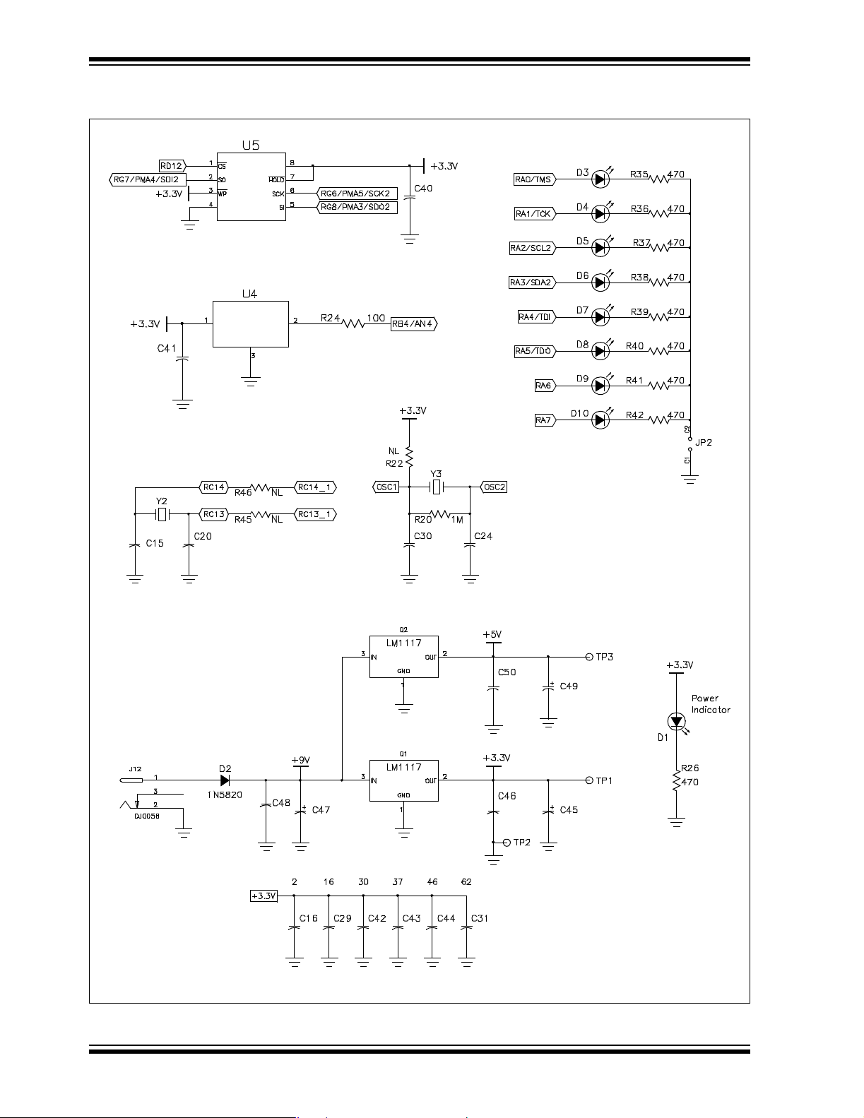
There are two ways to supply power to the Explorer 16 board:
• An unregulated DC supply of 9V to 15V (preferably 9V) supplied to J12.
For default functionality, a power supply with a current capability of 250 mA is
sufficient. Since the board can serve as a modular development platform that can
connect to multiple expansion boards, voltage regulators (Q1 and Q2) with a
maximum current capability of 800 mA are used. This may require a larger power
supply of up to 1.6A. Because the regulators do not have heat sinks, long-term
operation at such loads is not recommended.
Note: The Explorer 16 kit does not include a power supply. If an external supply
is needed, use Microchip part number AC162039.
• An external, regulated DC power supply that provides both +5V and +3.3V can be
connected to the terminals provided (at the bottom left side of the board, near S3).
Note: Do not attempt to power the Explorer 16 board using the MPLAB ICD 2
module. It is not designed to be a USB bus power source.
One green LED (D1) is provided to show when the Explorer 16 board is powered up.
The power-on LED indicates the presence of +3.3V.
© 2005 Microchip Technology Inc. DS51589A-page 27
Page 32

Explorer 16 Development Hardware
4.2.3 RS-232 Serial Port
An RS-232 level shifter (U3) has been provided with all necessary hardware to support
RS-232 connection with hardware flow control through the DB9 connector. The port is
configured as a DCE device, and can be connected to a PC using a straight-through
cable.
The PIC24/dsPIC33F RX and TX pins are tied to the RX and TX lines of U3. The
PIC24/dsPIC33F RTS and CTS pins are tied to the RX2 (DIN2) and TX2 (DOUT2) lines
of the MAX3232 for hardware flow control.
4.2.4 Temperature Sensor
An analog output thermal sensor (Microchip TC1074A, U4) is connected to one of the
controller’s A/D channels.
4.2.5 USB Connectivity
The Explorer 16 board includes a PIC18LF4550 USB microcontroller, which provides
both USB connectivity and support for protocol translation. The PIC18LF4550 is
hard-wired to the PIC24/dsPIC33F devices to provide three types of connectivity:
• SPI™ of PIC18LF4550 to SPI1 of PIC24/dsPIC33F
• I/O pins of PIC18LF4550 to ICSP™ pins of PIC24/dsPIC33F
• I/O pins of PIC18LF4550 to JTAG pins of PIC24/dsPIC33F
The type of connectivity depends on the firmware installed on the PIC18LF4550. At the
time of initial release, the PIC18LF4550 is loaded with USB bootloader firmware, which
permits easy upgrades of connectivity firmware over the USB. Installing this firmware
is described in Appendix B. “Updating the USB Connectivity Firmware”.
PIC24 and dsPIC33F devices both have some 5V tolerant input pins. If a 5V tolerant
input is connected to the PIC18LF4550, protection diodes on the PIC18LF4550
device’s port pins will limit inputs to V
16-bit devices are 5V tolerant, refer to the appropriate device data sheet.
DD. For more information on which pins of the
4.2.6 ICD Connector
An MPLAB ICD 2 module can be connected by way of the modular connector (JP1) for
low-cost debugging. The ICD connector utilizes port pins, RB6 and RB7 of the
microcontroller, for in-circuit debugging.
Jumper J7 decides the terminus of the ICD 2 connector. If the jumper is set to the
“PIC24” side, JP1 communicates directly with RB6/RB7 of the PIM or on-board device
(determined by S2). If the jumper is set to the “F4450” side, JP1 communicates with the
on-board PIC18LF4550 USB device.
4.2.7 LCD
The Explorer 16 board includes an alphanumeric LCD display with two lines of 16 characters each. The display is driven with three control lines (RD4, RD5 and RD15) and
eight data lines (RE7:RE0). On PIC24 devices, the LCD is driven by the PMP module,
not the I/O port.
The Explorer 16 board has multiple LCD footprints and support options, although only
one footprint is ever populated at one time. The Lumex LCM-SO1062 (populated at
LCD4) is a 5V LCD with TTL input, and is used in the initial version of the Explorer 16
board. The Tianma TM162JCAWG1 (populated at LCD1) is a 3V LCD; it is anticipated
to be used in future versions of the board.
An alternate configuration option allows the use of RD3:RD0 as four of the data lines,
instead of RE7:RE4. To do this, the user must cut the trace jumpers at R60/62/64/66
and create solder bridges from the pads for R61/63/65/67 (see Figure 4-1).
© 2005 Microchip Technology Inc. DS51589A-page 28
Page 33

Explorer 16 Development Board User’s Guide
FIGURE 4-1: MODIFICATIONS TO R60-R67 FOR LCD CONFIGURATION
(SCALE ENHANCED FOR VISIBILITY)
Add
Solder
Bridges
Here
Cut Traces
Here
R62
R60
R63
R61
R66
R64
R67
R65
4.2.8 Graphic LCD
The Explorer 16 also has a footprint and layout support for the Optrex 128 x 64 dot-matrix
graphic LCD (part number F-51320GNB-LW-AB) and associated circuitry. This is the
same display used in Microchip’s MPLAB PM3 programmer.
4.2.9 Switches
Five push button switches provide the following functions:
• S1: Active-low MCLR
• S3: Active-low switch connected to RD6 (user-defined)
• S4: Active-low switch connected to RD13 (user-defined)
• S5: Active-low switch connected to RA7 (user-defined)
• S6: Active-low switch connected to RD7 (user-defined)
Switch S1 has a debounce capacitor, whereas S3 through S6 do not; this allows the
user to investigate debounce techniques. When Idle, the switches are pulled high
(+3.3V). When pressed, they are grounded.
switch to hard reset the processor
4.2.10 Analog Input (Potentiometer)
A 10 kΩ potentiometer is connected through a series resistor to AN5. It can be adjusted
from V
DD to GND to provide an analog input to one of the controller’s A/D channels.
4.2.11 LEDs
Eight red LEDs (D2 through D9) are connected to PORTA of the PIM socket. The
PORTA pins are set high to light the LEDs. These LEDs may be disabled by removing
jumper JP2.
4.2.12 Oscillator Options
The installed microcontroller has two separate oscillator circuits connected.The main
oscillator uses an 8 MHz crystal (Y3) and functions as the controller’s primary oscillator.
A second circuit, using a 32.768 kHz (watch type) crystal (Y2), functions as the Timer1
oscillator and serves as the source for the RTCC and secondary oscillator.
The PIC18LF4550, at the heart of the USB subsystem, is independently clocked and
has its own 20 MHz crystal (Y1).
4.2.13 Serial EEPROM
A 25LC256 256K (32K x 8) serial EEPROM (U5) is included for nonvolatile firmware
storage. It is also used to demonstrate SPI bus operation.
DS51589A-page 29 © 2005 Microchip Technology Inc.
Page 34

Explorer 16 Development Hardware
4.2.14 PICkit 2 Connector
Connector J14 provides the footprint for a 6-pin PICkit 2 programmer interface. This will
provide a third low-cost programming option, besides MPLAB ICD 2 and the JTAG
interface, when PICkit 2 support for larger devices become available in the future.
4.2.15 JTAG Connector
Connector J13 provides a standard JTAG interface, allowing users to connect to and
program the controller via JTAG.
4.2.16 PICtail™ Plus Card Edge Modular Expansion Connectors
The Explorer 16 board has been designed with the PICtail™ Plus modular expansion
interface, allowing the board to provide basic generic functionality and still be easily
extendable to new technologies as they become available.
PICtail Plus is based on a 120-pin connection divided into three sections of 30 pins,
30 pins and 56 pins. The two 30-pin connections have parallel functionality; for example, pins 1, 3, 5 and 7 have SPI1 functionality on the top 30-pin segment, with similar
SPI2 functionality on the corresponding pins in the middle 30-pin segment.
Each 30-pin section provides connections to all of the serial communications
peripherals, as well as many I/O ports, external interrupts and A/D channels. This provides enough signals to develop many different expansion interfaces, such as
Ethernet, Zigbee™, IrDA
used in either the top or middle 30-pin sections.
The Explorer 16 board provides footprints for two edge connectors for daughter cards,
one populated (J5, Samtec # MEC1-160-02-S-D-A) and one unpopulated (J6). The
board also has a matching male edge connection (J9), allowing it to be used as an
expansion card itself.
®
and so on. The 30-pin PICtail Plus expansion boards can be
4.2.16.1 CROSSOVER CONNECTIONS FOR SPI AND UART
The PICtail Plus interface allows two Explorer 16 boards to be connected directly to
each other without any external connector. This provides 1-to-1 connection between
the microcontrollers on the two boards, an interface that works well for many types of
peripherals (I
and UARTs, require cross-wire connections; that is, the TX (or SDO) pin of one
controller must be connected to the RX (or SDI) of the other and vice versa.
The Explorer 16 board uses two 74HCT4053 analog multiplexers to simplify the connections between itself and any daughter boards. U6 and U7 provide active control of
the cross-wire capability on SPI1 and UART1, with a hardware flow control signal
provided by three I/O pins.
The multiplexers are controlled by the state of pins RB12, RB13 and RB14. When a
control pin is high (the default state), the corresponding SPI1 or UART1 pin pairs are
connected to their default pins on the PICtail Plus interface. When a control pin is
asserted low, the corresponding pin pair functions are swapped. Table 4-1 details the
relationship between the control pins and SPI1/UART1 functions on the interface.
2
C, PMP, etc.). However, certain serial peripheral modules, such as SPIs
© 2005 Microchip Technology Inc. DS51589A-page 30
Page 35

Explorer 16 Development Board User’s Guide
TABLE 4-1: LOCATION OF SPI1 AND UART1 PINS ON PICtail™ PLUS
INTERFACE
UART1 Control Pins SPI1
Control
Pin State
1 24192057
0 42201975
Note: When connecting SPI and UART peripherals on two Explorer 16 boards,
Control Pin RB14 Control Pin RB13 Control Pin RB12
U1RX U1TX U1CTS
U1RTS SDI1 SDO1
use crossover connection on only one of the boards.
DS51589A-page 31 © 2005 Microchip Technology Inc.
Page 36

NOTES:
Explorer 16 Development Hardware
© 2005 Microchip Technology Inc. DS51589A-page 32
Page 37

EXPLORER 16 DEVELOPMENT
BOARD USER’S GUIDE
Appendix A. Explorer 16 Development Board Schematics
A.1 INTRODUCTION
This section provides detailed technical information on the Explorer 16 board.
A.2 DEVELOPMENT BOARD BLOCK DIAGRAM
FIGURE A-1: HIGH-LEVEL BLOCK DIAGRAM OF THE EXPLORER 16 DEVELOPMENT BOARD
USB
9-15 VDC
PIC18LF4550
ICD/ICSP
JTAG
+3.3V and
+5V Supply
Temperature
Sensor
SPI*
ICSP*
JTAG*
PIC24FJ128GA010
dsPIC33FJ256GP710
RS-232
Transceiver
16x2 LCD Display
SPI
EEPROM
POT
LEDs
Switches
PICtail™ Plus
Modular Expansion
Connector
PICtail™ Plus
* Hardware support only; firmware support for SPI™, JTAG and ICSP™ via USB are not available at this time.
© 2005 Microchip Technology Inc. DS51589A-page 33
Page 38

Explorer 16 Development Board Schematics
A.3 DEVELOPMENT BOARD SCHEMATICS
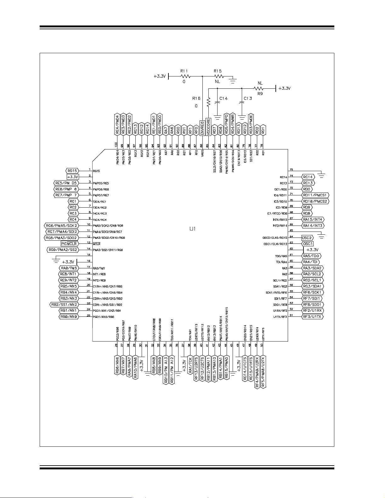
FIGURE A-2: EXPLORER 16 BOARD SCHEMATIC, SHEET 1 OF 8 (PIM SOCKET)
VDDCORE
VDD
VSS
VDD
VSS
VCAP/VDDCORE
VSS
VDD
100-Pin PIM
AVSS
AVDD
VDD
VSS
VDD
VSS
CVREF/AN10/RB10
© 2005 Microchip Technology Inc. DS51589A-page 34
Page 39
Explorer 16 Development Board User’s Guide
FIGURE A-3: EXPLORER 16 BOARD SCHEMATIC, SHEET 2 OF 8 (BOARD MOUNTED
PIC24FJ128GA010 MCU, WHEN INSTALLED)
VDD
VSS
VDD
VCAP/VDDCORE
PIC24FJ128GA010
10 μF
.1 μF
VSS
VSS
VDD
SS
AVDD
CVREF/AN10/RB10
VSS
AVSS
VDD
V
VDD
DS51589A-page 35 © 2005 Microchip Technology Inc.
Page 40

Explorer 16 Development Board Schematics
FIGURE A-4: EXPLORER 16 BOARD SCHEMATIC, SHEET 3 OF 8 (MPLAB® ICD 2, JTAG,
PICkit™ 2 AND PICtail™ Plus CONNECTORS)
MPLAB® ICD 2 Connector
.1 μF
PICkit™ 2 Programmer
© 2005 Microchip Technology Inc. DS51589A-page 36
Page 41

Explorer 16 Development Board User’s Guide
FIGURE A-5: EXPLORER 16 BOARD SCHEMATIC, SHEET 4 OF 8 (PICtail™ PLUS EDGE AND
SOCKET CONNECTORS)
DS51589A-page 37 © 2005 Microchip Technology Inc.
Page 42

Explorer 16 Development Board Schematics
FIGURE A-6: EXPLORER 16 BOARD SCHEMATIC, SHEET 5 OF 8 (SWITCHES,
MULTIPLEXERS AND POTENTIOMETER)
VCC
.1 μF
VEE
VCC
VEE
.1 μF
.1 μF
© 2005 Microchip Technology Inc. DS51589A-page 38
Page 43
Explorer 16 Development Board User’s Guide
FIGURE A-7: EXPLORER 16 BOARD SCHEMATIC, SHEET 6 OF 8 (EEPROM, TEMPERATURE
SENSOR, LEDs, OSCILLATOR CIRCUITS AND POWER SUPPLY)
VCC
32 kHz
22 pF
.1 μF
22 pF
VSS
VDD
25LC256
TC1047A
VSS
.1 μF
V
OUT
8 MHz
22 pF
22 pF
47 μF
47 μF
.1 μF
47 μF
.1 μF
.1 μF
.1 μF
.1 μF
.1 μF
.1 μF
.1 μF
.1 μF
DS51589A-page 39 © 2005 Microchip Technology Inc.
Page 44

Explorer 16 Development Board Schematics
FIGURE A-8: EXPLORER 16 BOARD SCHEMATIC, SHEET 7 OF 8 (USB AND
UART SUBSYSTEMS)
VBUS
VUSB
VSS
VSS
VDD
VDD
.1 μF
.1 μF
22 pF
.1 μF
.1 μF
PIC18F4550_QFN44
VSS
VDD
VDD
20 MHz
22 pF
.1 μF
.1 μF
.1 μF
.1 μF
VCC
.1 μF
.1 μF
© 2005 Microchip Technology Inc. DS51589A-page 40
Page 45

Explorer 16 Development Board User’s Guide
FIGURE A-9: EXPLORER 16 BOARD SCHEMATIC, SHEET 8 OF 8 (LCDs AND OPTIONAL
LCD CONNECTIONS)
Alternative LCD Configurations:
V
O
V
EE
V
CC
4.7 μF
4.7 μF
1 μF
1 μF
4.7 μF
4.7 μF
1 μF
1 μF
1 μF
.1 μF
V
V
V
EE
EE
EE
V
CC
V
SS
V
DD
V
O
DS51589A-page 41 © 2005 Microchip Technology Inc.
Page 46

NOTES:
Explorer 16 Development Board Schematics
© 2005 Microchip Technology Inc. DS51589A-page 42
Page 47

EXPLORER 16 DEVELOPMENT
BOARD USER’S GUIDE
Appendix B. Updating the USB Connectivity Firmware
B.1 INTRODUCTION
The USB subsystem of the Explorer 16 Development Board is preprogrammed with
USB bootloader firmware. This provides an easy method for upgrading the
PIC18LF4550 firmware to support ICSP, JTAG and SPI connectivity to PIC24 and
dsPIC33F devices.
This chapter describes how to upgrade the PIC18LF4550 device’s firmware with the
PICkit 2 software. The same process can be used to upgrade the PIC18LF4550
device’s firmware when updates and new firmware packages become available.
B.2 UPDATING THE PICkit 2 MICROCONTROLLER PROGRAMMER
Before beginning, it will be necessary to obtain and install the PICkit 2 programmer
software. Complete instructions for installing and using the programmer software
application is provided in the
(DS51553). The programmer and user’s guide, as well as the latest version of the
PICkit 2 operating system firmware, are available from the Microchip corporate
web site, www.microchip.com.
To update the USB firmware:
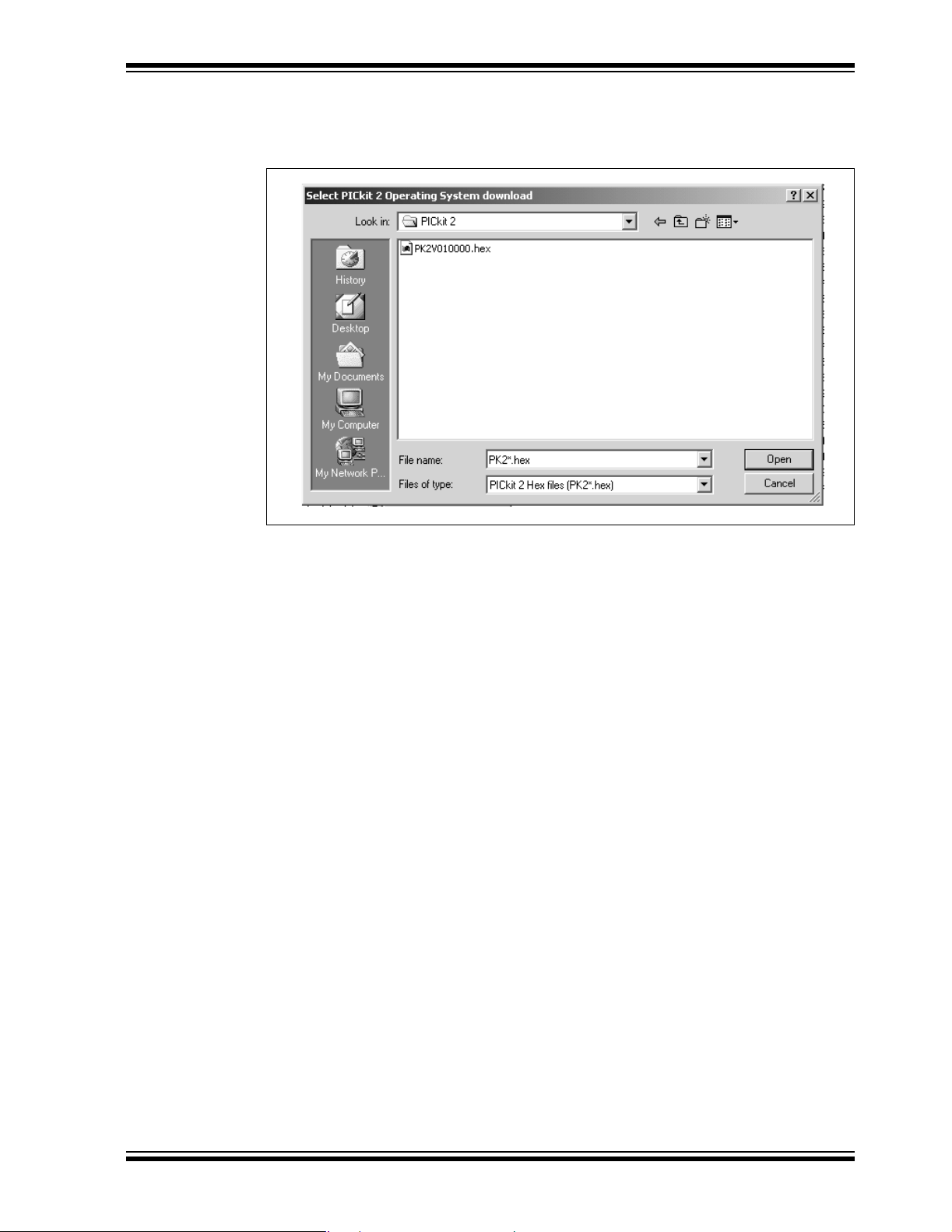
1. If not done already, download the latest PICkit 2 operating system software from
the Microchip web site.
2. On the Explorer 16 board, install a jumper between pins 9 and 10 of the JTAG
connector (J13).
3. Press and release MCLR
mode and makes it ready to accept new code.
4. Connect the Explorer 16 board to the PC via a standard USB cable.
5. Launch the PICkit 2 programmer software. From the menu bar, select
Tools > Download PICKit 2 Operating System
PICkit™ 2 Microcontroller Programmer User’s Guide
(S1). This places the USB subsystem in Bootloader
(Figure B-1).
FIGURE B-1: DOWNLOAD PICkit™ 2 OPERATING SYSTEM
© 2005 Microchip Technology Inc. DS51589A-page 43
Page 48
Updating the USB Connectivity Firmware
6. Browse to the directory where the latest operating system firmware was saved
(Figure B-2).
FIGURE B-2: SELECT PICkit™ 2 OPERATING SYSTEM
7. Select the PK2_Explorer16_*.hex file and click the Open button.
The progress of the update is displayed in the status bar of the programming software.
When the update completes successfully, the status bar displays “Operating System
Verified”. The update is now complete.
B.3 OTHER USB FIRMWARE UPDATES
It is anticipated that various USB connectivity firmwares will be made available in the
future. Users are encouraged to periodically check the Microchip web site
(www.microchip.com) for new and revised code.
© 2005 Microchip Technology Inc. DS51589A-page 44
Page 49

EXPLORER 16 DEVELOPMENT
BOARD USER’S GUIDE
Index
B
Build Options............................................................ 16
C
Configuration Bits..................................................... 19
Crossover Connections
(Serial Communications) ...................................8, 30
Customer Change Notification Service ...................... 5
Customer Support...................................................... 5
D
Documentation
Conventions........................................................ 2
Layout ................................................................. 1
dsPIC33 Tutorial Program........................................ 25
dsPIC33F Tutorial Program
Flowchart .......................................................... 26
E
Explorer 16 Development Board
Block Diagram .................................................. 33
Layout ................................................................. 9
Schematics ..................................................34
Explorer 16 Programming Tutorial ........................... 11
Building the Code ............................................. 16
Creating the Project.......................................... 12
Programming the Device .................................. 19
–41
F
Free Software Foundation ......................................... 4
G
GNU Language Tools ................................................ 4
H
Hardware Features
Analog Potentiometer ....................................8
ICD Connector ...............................................8
JTAG Connector............................................8
LCD, Alphanumeric........................................8
LCD, Graphic .................................................8
LEDs ..............................................................8
Multiplexers....................................................8
Oscillator Options ..........................................8
PICkit 2 Connector.........................................8
PICtail Plus Card Edge Connectors...............8
Power Indicator LED........................................... 8
Power Supply.................................................8
, 29
, 28
, 30
, 28
, 29
, 29
, 30
, 29
, 30
, 30
, 27
Processor Support ........................................ 8
Prototype Area.................................................... 8
RS-232 Serial Port........................................ 8, 28
Serial EEPROM ............................................ 8
Switches........................................................ 8
Temperature Sensor..................................... 8
USB Connectivity.......................................... 8
, 27
, 29
, 29
, 28
, 28
I
Internet Address......................................................... 4
L
Language Toolsuite.................................................. 13
M
Microchip Internet Web Site ....................................... 4
MPLAB ICD 2........................................................... 10
MPLAB IDE Simulator, Editor User’s Guide............... 4
P
PIC24 Tutorial Program ........................................... 23
Flowchart .......................................................... 24
PICtail Plus Edge Connectors
Use with Crossover Serial
Connections........................................ 30
Project ...................................................................... 12
Project Wizard.......................................................... 12
R
Reading, Recommended ........................................... 3
Readme...................................................................... 3
Reference Documents ............................................. 10
S
Schematics......................................................... 34–41
U
USB
Connectivity ...................................................... 28
Updating the USB Connectivity
Firmware.............................................43
W
Warranty Registration ................................................ 2
Workspace ............................................................... 12
WWW Address........................................................... 4
© 2005 Microchip Technology Inc. DS51589A-page 45
Page 50

WORLDWIDE SALES AND SERVICE
AMERICAS
Corporate Office
2355 West Chandler Blvd.
Chandler, AZ 85224-6199
Tel: 480-792-7200
Fax: 480-792-7277
Technical Support:
http://support.microchip.com
Web Address:
www.microchip.com
Atlanta
Alpharetta, GA
Tel: 770-640-0034
Fax: 770-640-0307
Boston
Westborough, MA
Tel: 774-760-0087
Fax: 774-760-0088
Chicago
Itasca, IL
Tel: 630-285-0071
Fax: 630-285-0075
Dallas
Addison, TX
Tel: 972-818-7423
Fax: 972-818-2924
Detroit
Farmington Hills, MI
Tel: 248-538-2250
Fax: 248-538-2260
Kokomo
Kokomo, IN
Tel: 765-864-8360
Fax: 765-864-8387
Los Angeles
Mission Viejo, CA
Tel: 949-462-9523
Fax: 949-462-9608
San Jose
Mountain View, CA
Tel: 650-215-1444
Fax: 650-961-0286
Toronto
Mississauga, Ontario,
Canada
Tel: 905-673-0699
Fax: 905-673-6509
ASIA/PACIFIC
Australia - Sydney
Tel: 61-2-9868-6733
Fax: 61-2-9868-6755
China - Beijing
Tel: 86-10-8528-2100
Fax: 86-10-8528-2104
China - Chengdu
Tel: 86-28-8676-6200
Fax: 86-28-8676-6599
China - Fuzhou
Tel: 86-591-8750-3506
Fax: 86-591-8750-3521
China - Hong Kong SAR
Tel: 852-2401-1200
Fax: 852-2401-3431
China - Qingdao
Tel: 86-532-8502-7355
Fax: 86-532-8502-7205
China - Shanghai
Tel: 86-21-5407-5533
Fax: 86-21-5407-5066
China - Shenyang
Tel: 86-24-2334-2829
Fax: 86-24-2334-2393
China - Shenzhen
Tel: 86-755-8203-2660
Fax: 86-755-8203-1760
China - Shunde
Tel: 86-757-2839-5507
Fax: 86-757-2839-5571
China - Wuhan
Tel: 86-27-5980-5300
Fax: 86-27-5980-5118
China - Xian
Tel: 86-29-8833-7250
Fax: 86-29-8833-7256
ASIA/PACIFIC
India - Bangalore
Tel: 91-80-2229-0061
Fax: 91-80-2229-0062
India - New Delhi
Tel: 91-11-5160-8631
Fax: 91-11-5160-8632
India - Pune
Tel: 91-20-2566-1512
Fax: 91-20-2566-1513
Japan - Yokohama
Tel: 81-45-471- 6166
Fax: 81-45-471-6122
Korea - Gumi
Tel: 82-54-473-4301
Fax: 82-54-473-4302
Korea - Seoul
Tel: 82-2-554-7200
Fax: 82-2-558-5932 or
82-2-558-5934
Malaysia - Penang
Tel: 60-4-646-8870
Fax: 60-4-646-5086
Philippines - Manila
Tel: 63-2-634-9065
Fax: 63-2-634-9069
Singapore
Tel: 65-6334-8870
Fax: 65-6334-8850
Taiwan - Hsin Chu
Tel: 886-3-572-9526
Fax: 886-3-572-6459
Taiwan - Kaohsiung
Tel: 886-7-536-4818
Fax: 886-7-536-4803
Taiwan - Taipei
Tel: 886-2-2500-6610
Fax: 886-2-2508-0102
Thailand - Bangkok
Tel: 66-2-694-1351
Fax: 66-2-694-1350
EUROPE
Austria - Wels
Tel: 43-7242-2244-399
Fax: 43-7242-2244-393
Denmark - Copenhagen
Tel: 45-4450-2828
Fax: 45-4485-2829
France - Paris
Tel: 33-1-69-53-63-20
Fax: 33-1-69-30-90-79
Germany - Munich
Tel: 49-89-627-144-0
Fax: 49-89-627-144-44
Italy - Milan
Tel: 39-0331-742611
Fax: 39-0331-466781
Netherlands - Drunen
Tel: 31-416-690399
Fax: 31-416-690340
Spain - Madrid
Tel: 34-91-708-08-90
Fax: 34-91-708-08-91
UK - Wokingham
Tel: 44-118-921-5869
Fax: 44-118-921-5820
10/31/05
DS51589A-page 46 © 2005 Microchip Technology Inc.
 Loading...