

Page 1

EVB-LAN9252-DIG-IO
EtherCAT® DIG I/O
Evaluation Board
User’s Guide
2014 Microchip Technology Inc. Preliminary DS50002332A
Page 2

Note the following details of the code protection feature on Microchip devices:
YSTEM
CERTIFIED BY DNV
== ISO/TS 16949 ==
• Microchip products meet the specification contained in their particular Microchip Data Sheet.
• Microchip believes that its family of products is one of the most secure families of its kind on the market today, when used in the
intended manner and under normal conditions.
• There are dishonest and possibly illegal methods used to breach the code protection feature. All of these methods, to our
knowledge, require using the Microchip products in a manner outside the operating specifications contained in Microchip’s Data
Sheets. Most likely, the person doing so is engaged in theft of intellectual property.
• Microchip is willing to work with the customer who is concerned about the integrity of their code.
• Neither Microchip nor any other semiconductor manufacturer can guarantee the security of their code. Code protection does not
mean that we are guaranteeing the product as “unbreakable.”
Code protection is constantly evolving. We at Microchip are committed to continuously improving the code protection features of our
products. Attempts to break Microchip’s code protection feature may be a violation of the Digital Millennium Copyright Act. If such acts
allow unauthorized access to your software or other copyrighted work, you may have a right to sue for relief under that Act.
Information contained in this publication regarding device applications and the like is provided only for your convenience and may be
superseded by updates. It is your responsibility to ensure that your application meets with your specifications. MICROCHIP MAKES NO
REPRESENTATIONS OR WARRANTIES OF ANY KIND WHETHER EXPRESS OR IMPLIED, WRITTEN OR ORAL, STATUTORY OR
OTHERWISE, RELATED TO THE INFORMATION, INCLUDING BUT NOT LIMITED TO ITS CONDITION, QUALITY, PERFORMANCE,
MERCHANTABILITY OR FITNESS FOR PURPOSE. Microchip disclaims all liability arising from this information and its use. Use of Microchip devices in life support and/or safety applications is entirely at the buyer’s risk, and the buyer agrees to defend, indemnify and hold
harmless Microchip from any and all damages, claims, suits, or expenses resulting from such use. No licenses are conveyed, implicitly or
otherwise, under any Microchip intellectual property rights.
Trademarks
The Microchip name and logo, the Microchip logo, dsPIC, FlashFlex, flexPWR, JukeBlox, K
MediaLB, MOST, MOST logo, MPLAB, OptoLyzer, PIC, PICSTART, PIC
UNI/O are registered trademarks of Microchip Technology Incorporated in the U.S.A. and other countries.
The Embedded Control Solutions Company and mTouch are registered trademarks of Microchip Technology Incorporated in the U.S.A.
Analog-for-the-Digital Age, BodyCom, chipKIT, chipKIT logo, CodeGuard, dsPICDEM, dsPICDEM.net, ECAN, In-Circuit Serial
Programming, ICSP, Inter-Chip Connectivity, KleerNet, KleerNet logo, MiWi, MPASM, MPF, MPLAB Certified logo, MPLIB, MPLINK,
MultiTRAK, NetDetach, Omniscient Code Generation, PICDEM, PICDEM.net, PICkit, PICtail, RightTouch logo, REAL ICE, SQI, Serial
Quad I/O, Total Endurance, TSHARC, USBCheck, VariSense, ViewSpan, WiperLock, Wireless DNA, and ZENA are trademarks of
Microchip Technology Incorporated in the U.S.A. and other countries.
SQTP is a service mark of Microchip Technology Incorporated in the U.S.A.
Silicon Storage Technology is a registered trademark of Microchip Technology Inc. in other countries.
GestIC is a registered trademarks of Microchip Technology Germany II GmbH & Co. KG, a subsidiary of Microchip Technology Inc., in
other countries.
All other trademarks mentioned herein are property of their respective companies.
© 2014, Microchip Technology Incorporated, Printed in the U.S.A., All Rights Reserved.
32
logo, RightTouch, SpyNIC, SST, SST Logo, SuperFlash and
EELOQ, KEELOQ logo, Kleer, LANCheck,
ISBN: 97816312769251
QUALITY MANAGEMENT S
DS50002332A-page 2 Preliminary 2014 Microchip Technology Inc.
Microchip received ISO/TS-16949:2009 certification for its worldwide
headquarters, design and wafer fabrication facilities in Chandler and
Tempe, Arizona; Gresham, Oregon and design centers in California
and India. The Company’s quality system processes and procedures
are for its PIC
devices, Serial EEPROMs, microperipherals, nonvolatile memory and
analog products. In addition, Microchip’s quality system for the design
and manufacture of development systems is ISO 9001:2000 certified.
®
MCUs and dsPIC® DSCs, KEELOQ
®
code hopping
Page 3

Object of Declaration: EVB-LAN9252-DIG-IO
2014 Microchip Technology Inc. Preliminary DS50002332A-page 3
Page 4

EVB-LAN9252-DIG-IO EtherCAT® DIG I/O User’s Guide
NOTES:
DS50002332A-page 4 Preliminary 2014 Microchip Technology Inc.
Page 5

EVB-LAN9252-DIG-IO
ETHERCAT® DIG I/O
USER’S GUIDE
Table of Contents
Preface ........................................................................................................................... 7
Introduction............................................................................................................ 7
Document Layout .................................................................................................. 7
Conventions Used in this Guide ............................................................................ 8
The Microchip Web Site ........................................................................................ 9
Development Systems Customer Change Notification Service ............................ 9
Customer Support ................................................................................................. 9
Document Revision History ................................................................................. 10
Chapter 1. Overview
1.1 Introduction ................................................................................................... 11
1.2 References ................................................................................................... 12
1.3 Terms and Abbreviations ............................................................................. 12
Chapter 2. Board Details & Configuration
2.1 Power ........................................................................................................... 13
2.1.1 +5V Power ................................................................................................. 13
2.2 Resets .......................................................................................................... 13
2.2.1 Power-on Reset ......................................................................................... 13
2.2.2 Reset Out .................................................................................................. 13
2.2.3 GPIO Reset ............................................................................................... 13
2.3 Clock ............................................................................................................ 14
2.4 Configuration ................................................................................................ 14
2.4.1 Strap Options ............................................................................................ 15
2.4.2 LED Indicators ........................................................................................... 17
2.4.3 EEPROM Switch ....................................................................................... 18
2.4.4 DIG INPUT Mode ...................................................................................... 18
2.4.5 DIG OUTPUT Mode .................................................................................. 18
2.4.6 DIG Bidirectional Mode ............................................................................. 19
2.4.7 Control Signals .......................................................................................... 19
2.5 Mechanicals ................................................................................................. 20
Chapter 3. LAN9252 EEPROM Programming
3.1 Programming the LAN9252 EEPROM ......................................................... 21
Appendix A. EVB-LAN9252-DIG-IO Evaluation Board
A.1 Introduction .................................................................................................. 24
Appendix B. EVB-LAN9252-DIG-IO Evaluation Board Schematics
B.1 Introduction .................................................................................................. 25
Appendix C. Bill of Materials (BOM)
C.1 Introduction .................................................................................................. 33
2014 Microchip Technology Inc. Preliminary DS50002332A-page 5
Page 6

EVB-LAN9252-DIG-IO EtherCAT® DIG I/O User’s Guide
Worldwide Sales and Service .....................................................................................37
DS50002332A-page 6 Preliminary 2014 Microchip Technology Inc.
Page 7

EVB-LAN9252-DIG-IO
ETHERCAT® DIG I/O
USER’S GUIDE
Preface
NOTICE TO CUSTOMERS
All documentation becomes dated, and this manual is no exception. Microchip tools and
documentation are constantly evolving to meet customer needs, so some actual dialogs
and/or tool descriptions may differ from those in this document. Please refer to our web site
(www.microchip.com) to obtain the latest documentation available.
Documents are identified with a “DS” number. This number is located on the bottom of each
page, in front of the page number. The numbering convention for the DS number is
“DSXXXXXA”, where “XXXXX” is the document number and “A” is the revision level of the
document.
For the most up-to-date information on development tools, see the MPLAB
Select the Help menu, and then Topics to open a list of available online help files.
®
IDE online help.
INTRODUCTION
This chapter contains general information that will be useful to know before using the
EVB-LAN9252-DIG-IO. Items discussed in this chapter include:
Document Layout
•
• Conventions Used in this Guide
• The Microchip Web Site
• Development Systems Customer Change Notification Service
• Customer Support
• Document Revision History
DOCUMENT LAYOUT
This document describes how to use the EVB-LAN9252-DIG-IO as a development tool for the
Microchip LAN9252 EtherCAT® slave controller. The manual layout is as follows:
• Chapter 1. “Overview” – Shows a brief description of the EVB-LAN9252-DIG-IO.
• Chapter 2. “Board Details & Configuration” – Includes details and instructions for using
the EVB-LAN9252-DIG-IO.
• Chapter 3. “LAN9252 EEPROM Programming” – Includes details and instructions for
programming the LAN9252 EEPROM.
• Appendix A. “EVB-LAN9252-DIG-IO Evaluation Board” – This appendix shows the
EVB-LAN9252-DIG-IO.
• Appendix B. “EVB-LAN9252-DIG-IO Evaluation Board Schematics” – This appendix
shows the EVB-LAN9252-DIG-IO schematics.
• Appendix C. “Bill of Materials (BOM)” – This appendix includes the
EVB-LAN9252-DIG-IO Bill of Materials (BOM).
2014 Microchip Technology Inc. Preliminary DS50002332A-page 7
Page 8
EVB-LAN9252-DIG-IO ETHERCAT® DIG I/O USER’S GUIDE
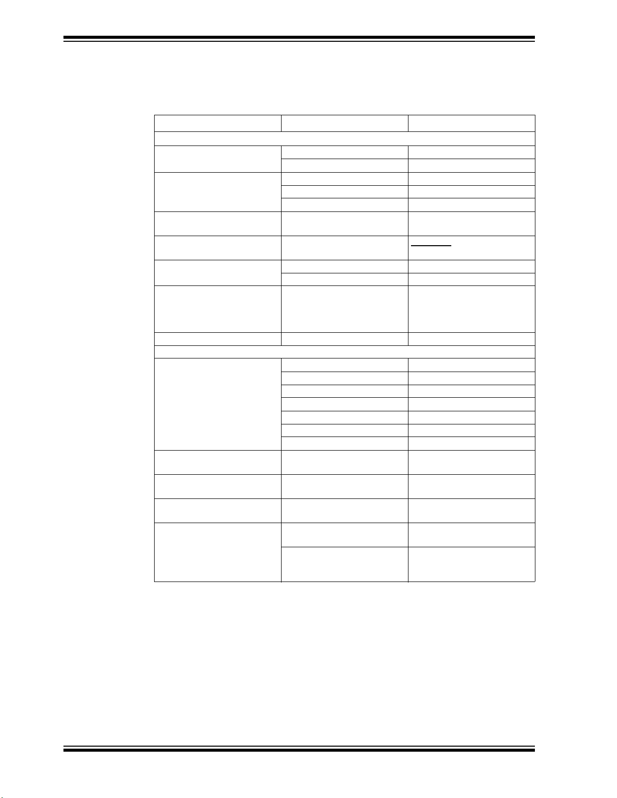
CONVENTIONS USED IN THIS GUIDE
This manual uses the following documentation conventions:
DOCUMENTATION CONVENTIONS
Description Represents Examples
Arial font:
Italic characters Referenced books MPLAB
Emphasized text ...is the only compiler...
Initial caps A window the Output window
A dialog the Settings dialog
A menu selection select Enable Programmer
Quotes A field name in a window or
dialog
Underlined, italic text with
right angle bracket
Bold characters A dialog button Click OK
N‘Rnnnn A number in verilog format,
Text in angle brackets < > A key on the keyboard Press <Enter>, <F1>
Courier New font:
Plain Courier New Sample source code #define START
Italic Courier New A variable argument file.o, where file can be
Square brackets [ ] Optional arguments mcc18 [options] file
Curly brackets and pipe
character: { | }
Ellipses... Replaces repeated text var_name [,
A menu path File>Save
A tab Click the Power tab
where N is the total number of
digits, R is the radix and n is a
digit.
Filenames autoexec.bat
File paths c:\mcc18\h
Keywords _asm, _endasm, static
Command-line options -Opa+, -Opa-
Bit values 0, 1
Constants 0xFF, ‘A’
Choice of mutually exclusive
arguments; an OR selection
Represents code supplied by
user
®
IDE User’s Guide
“Save project before build”
4‘b0010, 2‘hF1
any valid filename
[options]
errorlevel {0|1}
var_name...]
void main (void)
{ ...
}
DS50002332A-page 8 Preliminary 2014 Microchip Technology Inc.
Page 9

Preface
THE MICROCHIP WEB SITE
Microchip provides online support via our web site at www.microchip.com. This web site is used
as a means to make files and information easily available to customers. Accessible by using your
favorite Internet browser, the web site contains the following information:
• Product Support – Data sheets and errata, application notes and sample programs,
design resources, user’s guides and hardware support documents, latest software releases
and archived software
• General Technical Support – Frequently Asked Questions (FAQs), technical support
requests, online discussion groups, Microchip consultant program member listing
• Business of Microchip – Product selector and ordering guides, latest Microchip press
releases, listing of seminars and events, listings of Microchip sales offices, distributors and
factory representatives
DEVELOPMENT SYSTEMS CUSTOMER CHANGE NOTIFICATION SERVICE
Microchip’s customer notification service helps keep customers current on Microchip products.
Subscribers will receive e-mail notification whenever there are changes, updates, revisions or
errata related to a specified product family or development tool of interest.
To register, access the Microchip web site at www.microchip.com, click on Customer Change
Notification and follow the registration instructions.
The Development Systems product group categories are:
• Compilers – The latest information on Microchip C compilers, assemblers, linkers and
other language tools. These include all MPLAB C compilers; all MPLAB assemblers
(including MPASM assembler); all MPLAB linkers (including MPLINK object linker); and all
MPLAB librarians (including MPLIB object librarian).
• Emulators – The latest information on Microchip in-circuit emulators.This includes the
MPLAB REAL ICE and MPLAB ICE 2000 in-circuit emulators.
• In-Circuit Debuggers – The latest information on the Microchip in-circuit debuggers. This
includes MPLAB ICD 3 in-circuit debuggers and PICkit 3 debug express.
• MPLAB IDE – The latest information on Microchip MPLAB IDE, the Windows Integrated
Development Environment for development systems tools. This list is focused on the
MPLAB IDE, MPLAB IDE Project Manager, MPLAB Editor and MPLAB SIM simulator, as
well as general editing and debugging features.
• Programmers – The latest information on Microchip programmers. These include produc-
tion programmers such as MPLAB REAL ICE in-circuit emulator, MPLAB ICD 3 in-circuit
debugger and MPLAB PM3 device programmers. Also included are nonproduction development programmers such as PICSTART Plus and PIC-kit 2 and 3.
CUSTOMER SUPPORT
Users of Microchip products can receive assistance through several channels:
• Distributor or Representative
• Local Sales Office
• Field Application Engineer (FAE)
• Technical Support
Customers should contact their distributor, representative or field application engineer (FAE) for
support. Local sales offices are also available to help customers. A listing of sales offices and
locations is included in the back of this document.
Technical support is available through the web site at: http://www.microchip.com/support
2014 Microchip Technology Inc. Preliminary DS50002332A-page 9
Page 10

EVB-LAN9252-DIG-IO ETHERCAT® DIG I/O USER’S GUIDE
DOCUMENT REVISION HISTORY
DS50002332A (December 2014)
• Initial Release of this Document.
DS50002332A-page 10 Preliminary 2014 Microchip Technology Inc.
Page 11

1.1 INTRODUCTION
The LAN9252 is a 2-port EtherCAT® slave controller with dual integrated Ethernet
PHYs which each contain a full-duplex 100BASE-TX transceiver and support 100Mbps
(100BASE-TX) operation. 100BASE-FX is supported via an external fiber transceiver.
Each port receives an EtherCAT® frame, performs frame checking and forwards it to
the next port. Time stamps of received frames are generated when they are received.
The Loop-back function of each port forwards the frames to the next logical port if there
is either no link at a port, if the port is not available, or if the loop is closed for that port.
The Loop-back function of port 0 forwards the frames to the EtherCAT® Processing
Unit. The loop settings can be controlled by the EtherCAT® master.
Packets are forwarded in the following order:
Port 0 -> EtherCAT® Processing Unit -> Port 1 -> Port 2.
The EtherCAT® Processing Unit (EPU) receives, analyzes and processes the EtherCAT® data stream. The main purpose of the EtherCAT® Processing unit is to enable
and coordinate access to the internal registers and the memory space of the ESC,
which can be addressed both from the EtherCAT® master and from the local application. Data exchange between master and slave applications is comparable to a
dual-ported memory (process memory), enhanced by special functions for consistency
checking (SyncManager) and data mapping (FMMU). Each FMMU performs bitwise
mapping of logical EtherCAT® system addresses to physical device addresses.
The scope of this document is to describe the EVB-LAN9252-DIG-IO setup, which supports a Digital I/O Interface and corresponding jumper configurations. The LAN9252 is
connected to an RJ45 Ethernet jack with integrated magnetics for 100BASE-TX connectivity. A simplified block diagram of the EVB-LAN9252-DIG-IO is shown in
Figure 1-1.
EVB-LAN9252-DIG-IO
ETHERCAT® DIG I/O
USER’S GUIDE
Chapter 1. Overview
2014 Microchip Technology Inc. Preliminary DS50002332A-page 11
Page 12

EVB-LAN9252-DIG-IO EtherCAT® DIG I/O User’s Guide
Microchip
LAN9252
EEPROM
EVB-LAN9252-DIG-IO
Straps
Port 0 Port 1
Oscillator
Power
Supply
Module
Control
Signals
5V
07815
07815
Jumper Selection
LEDs LEDs
Switches Switches
Digital I/O Circuit
100BASE-TX
Ethernet
Magnetics &
RJ45
100BASE-TX
Ethernet
Magnetics &
RJ45
Ethernet Ethernet
Fiber-
SFP
Port 0
Fiber-
SFP
Port 1
FIGURE 1-1: EVB-LAN9252-DIG-IO BLOCK DIAGRAM
1.2 REFERENCES
1.3 TERMS AND ABBREVIATIONS
Concepts and material available in the following documents may be helpful when reading this document. Visit www.microchip.com for the latest documentation.
• LAN9252 Data Sheet
• AN 8.13 Suggested Magnetics
• EVB-LAN9252-DIG-IO Schematics
IDE - Integrated Development Environment
ESC - EtherCAT® Slave Controller
EVB - Engineering Validation Board
HAL - Hardware Abstraction Layer
HBI - Host Bus Interface
SPI - Serial Protocol Interface
SSC - Slave Stack Code
DS50002332A-page 12 Preliminary 2014 Microchip Technology Inc.
Page 13

Chapter 2. Board Details & Configuration
2.1 POWER
EVB-LAN9252-DIG-IO
ETHERCAT® DIG I/O
USER’S GUIDE
This section includes sub-sections on the following EVB-LAN9252-DIG-IO details:
•Power
• Resets
• Clock
• Configuration
• Mechanicals
2.1.1 +5V Power
Power is supplied to the LAN9252 by a +3.3V on-board regulator, which is powered by
a +5V external wall adapter (Manufacturer: TRIAD MAGNETICS and P/N:
WSU050-3000). The LAN9252 includes an internal +1.2V regulator which supplies
power to the internal core logic. Assertion of the D1 Green LED indicates successful
generation of +3.3V output. The SW1 switch must be in the ON position for the +5V to
power the +3.3V regulator.
2.2 RESETS
2.2.1 Power-on Reset
A power-on reset occurs whenever power is initially applied to the LAN9252 or if the
power is removed and reapplied to the LAN9252. This event resets all circuitry within
the LAN9252. After initial power-on, the LAN9252 can be reset by pressing the reset
switch SW2. The reset LED D2 will assert (red) if when the LAN9252 is in reset condition. For stability, a delay of approximately 180ms is added from the +3.3V output to
reset release.
2.2.2 Reset Out
The LAN9252 reset pin can be configured as an output to reset the SoC. The RST# pin
becomes an open-drain output and is asserted for the minimum required time of 80ms.
2.2.3 GPIO Reset
The EVB-LAN9252-DIG-IO provides the option to reset the LAN9252 through a PIC
GPIO pin [95(RG14)]. The SW10 switch is used for this selection, as shown in
Ta bl e 2 -1 .
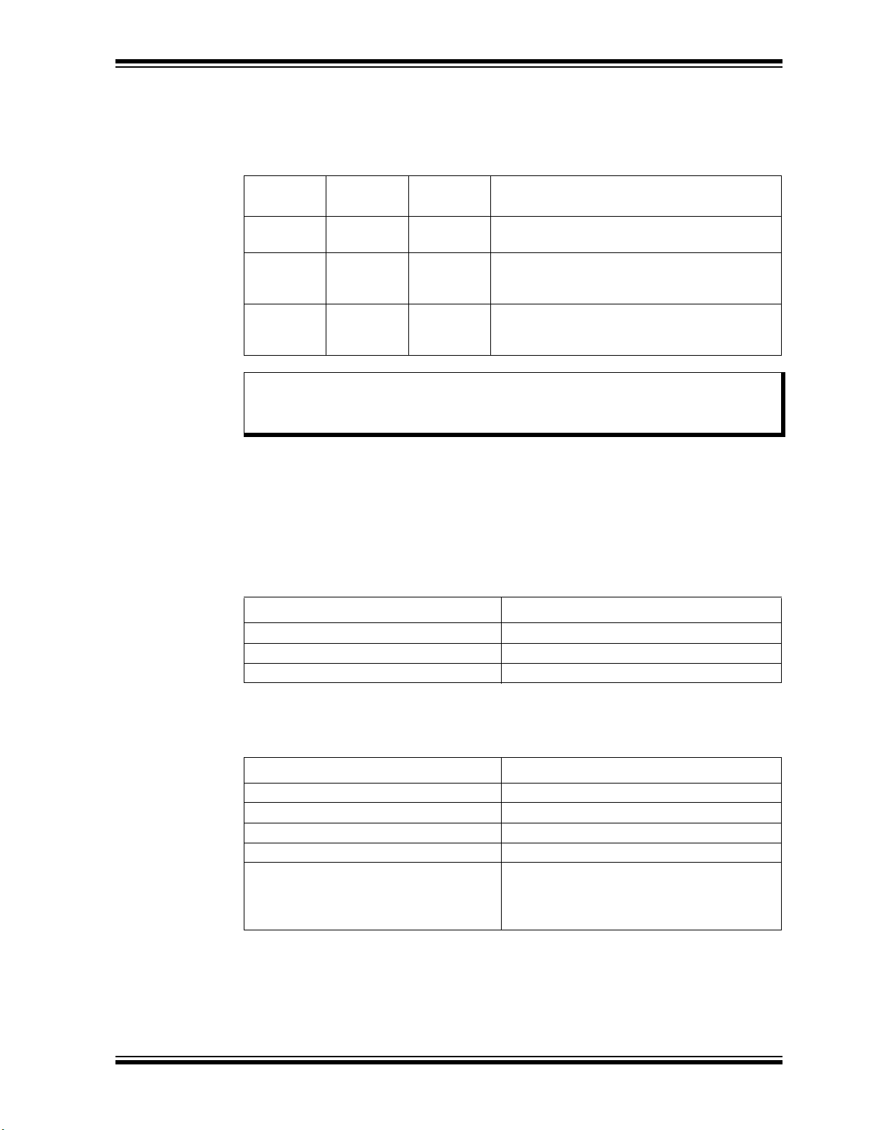
TABLE 2-1: RESET CONFIGURATION SWITCH
Switch Short Pins Knob Position Function
SW10 1-3 1-2 System Reset (SYS_RST) (Default)
SW10 1-2 1-3 GPIO Reset (GPIO_RST)
2014 Microchip Technology Inc. Preliminary DS50002332A-page 13
Page 14

EVB-LAN9252-DIG-IO EtherCAT® DIG I/O User’s Guide
Input Switches
Digital Output
LEDs
Digital I/O
Control Signals
PowerReset
RJ45
(with Magnetics)
Port 1Port 0
EEPROMStraps
Microchip
LAN9252
2.3 CLOCK
The EVB-LAN9252-DIG-IO utilizes an external 25Mhz 25ppm crystal from Cardinal
Components Inc. (P/N: CSM1Z-A5B2C5-40-25.0D18-F).
2.4 CONFIGURATION
The following sub-sections describe the various board features and configuration settings. A top view of the EVB-LAN9252-DIG-IO is shown in Figure 2-1.
FIGURE 2-1: EVB-LAN9252-DIG-IO TOP VIEW WITH CALLOUTS
DS50002332A-page 14 Preliminary 2014 Microchip Technology Inc.
Page 15

Board Details & Configuration
2.4.1 Strap Options
2.4.1.1 CHIP MODE SELECTION
Table 2-2 details the LAN9252 chip mode configuration straps.
TABLE 2-2: CHIP MODE CONFIGURATION STRAP
Header Description Pins Settings
J4,J5,J7,J8 Chip mode configuration strap
inputs. This strap determines
the number of active ports and
port types.
Note: For proper operation, chip mode must be in 2-port mode, where Port 0 =
PHY A and Port 1 = PHY B. This requires J4, J5, J7, and J8 to be
pulled-down (2-3) shorted. All other configurations are not supported by this
EVB.
2.4.1.2 EEPROM SIZE CONFIGURATION
The EEPROM size configuration strap (J6 & J9) determines the supported EEPROM
size range. A low selects 1Kbits (128 x 8) through 16Kbits (2K x 8)_24C16. A high
selects 32Kbits (4K x 8) through 512Kbits (64K x 8) or 4Mbits (512K x 8)_24C512.
1-2
Short 1-2 for high (pull-up)
2-3
Short 2-3 for low (pull-down) (default)
TABLE 2-3: EEPROM SIZE CONFIGURATION STRAP
Header Description Pins Settings
J6, J9 EEPROM size configuration
strap inputs. This strap determines the supported
EEPROM size range.
1-2
Short 1-2 for high (pull-up) (default)
2-3
Short 2-3 for low (pull-down)
2.4.1.3 COPPER AND FIBER STRAPS
The LAN9252 supports 100BASE-TX (Copper) and 100BASE-FX (Fiber) modes. In
100BASE-FX operation, the quality of the receive signal is provided by the external
transceiver as either an open-drain, CMOS level, Loss of Signal (SFP) or a LVPECL
Signal Detect (SFF).
This EVB supports 100BASE-TX (Copper) and SFP 100BASE-FX (Fiber) modes. By
default Copper Mode is active. Fiber Mode is supported as an assembly option. To
select the Copper or Fiber Mode, the respective strap and signal routing resister
assembly options must to be configured.
Note: Vendor part number for SFP: Finisar/FTLF1217P2,
for SFF: Avago Technologies US Inc/AFCT-5971LZ
2014 Microchip Technology Inc. Preliminary DS50002332A-page 15
Page 16
EVB-LAN9252-DIG-IO EtherCAT® DIG I/O User’s Guide
2.4.1.3.1 Copper Mode
The EVB-LAN9252-DIG-IO is set to Copper Mode by default. Table 2-4 details the
required strap resistor settings for Copper Mode operation.
TABLE 2-4: COPPER MODE STRAP RESISTORS
Resistors Description
R79 (10K) Configures Port 0 & 1 to Copper Mode
R76, R80 (10K) Configures Port 0 and Port 1 to Copper Mode, respectively
Note: R75, R77, and R78 must not be populated (DNP).
Additionally, the signal routing resistors detailed in Table 2-5 must be assembled for
Copper Mode operation.
TABLE 2-5: COPPER MODE SIGNAL ROUTING RESISTORS
Resistors Description
R17, R19, R21, R23 Port 0 Copper Mode enabled
R31, R33, R35, R37 Port 1 Copper mode enabled
Note: R16, R18, R20, R22, R30, R32, R34, and R36 (0402 package) must not be
populated (DNP).
2.4.1.3.2 Fiber Mode
The EVB-LAN9252-DIG-IO supports SFP type 100BASE-FX. To enabled Fiber Mode,
the respective strap and signal routing registers must be configured.
Note: Copper Mode related resistors must be DNP while Fiber Mode is active
(See Section 2.4.1.3.1 “Copper Mode”).
Table 2-6 details the required strap resistor settings for Fiber Mode operation.
TABLE 2-6: FIBER MODE STRAP RESISTORS
Resistors Description
R77 (10K) Configures Port 0 & 1 to FX-LOS Mode
R75, R78 (10K) Configures Port 0 and Port 1 to Fiber Mode, respectively
Note: R76, R79, and R80 must not be populated (DNP).
Additionally, the signal routing resistors detailed in Table 2-7 must be assembled for
Fiber Mode operation.
TABLE 2-7: FIBER MODE SIGNAL ROUTING RESISTORS
Resistors Description
R16, R18, R20, R22 Port 0 Fiber Mode enabled
R30, R32, R34, R36 Port 1 Fiber mode enabled
Note: R17, R19, R21, R23, R31, R33, R35, and R37 (0402 package) must not be
populated (DNP).
DS50002332A-page 16 Preliminary 2014 Microchip Technology Inc.
Page 17
Board Details & Configuration
2.4.1.3.3 FX-LOS Fiber Mode Strap
FX-LOS strap details are shown in Table 2-8. These strap settings determine if the
ports are to operate in FX-LOS Fiber Mode or FX-SD/Copper Mode.
TABLE 2-8: FX-LOS MODE STRAP SETTINGS
R77 (10K) R79 (10K)
Populate DNP 3.3 A level above 2V selects FX-LOS for Port 0 and
Populate Populate 1.5 A level of 1.5V selects FX-LOS for Port 0 and
DNP Populate 0 (Default) A level of 0V selects FX-SD / copper twisted pair
Note: The above strap details describe the LAN9252 function. This EVB does not
support SFF Fiber Mode. Therefore, FX-SD related straps are not applicable.
Reference
Volta g e ( V )
Function
Port 1
FX-SD / copper twisted pair for Port 1, further
determined by FXSDB
for Ports 0 and 1, further determined by FXSDA
and FXSDB
2.4.2 LED Indicators
The D3 and D4 LEDs are used to indicate the Link/Activity status on the corresponding
EVB ports, as detailed in Table 2-9. The Link/Act LED should be ON at each port when
the cable is present. If the Link/Act LED is not ON, it indicates there is an issue with the
connection or cable.
TABLE 2-9: D3 AND D4 LINK/ACTIVITY LED STATUS INDICATORS
State Description
Off Link is down
Flashing Green Link is up with activity
Steady Green Link is up with no activity
Additionally, the D5 LED is used as a RUN indicator (green) to shows the AL status of
the EtherCAT® State Machine (ESM), as detailed in Table 2-10.
TABLE 2-10: D5 RUN LED STATUS INDICATOR
State Description
Off The device is in the INITIALIZATION state
Blinking (on 200ms, off 200ms) The device is in the PRE-OPERATIONAL state
Single Flash (on 200ms, off 1000ms) The device is in the SAFE-OPERATIONAL state
On The device is in the OPERATIONAL state
Flickering (on 50ms, off 50ms) The device is booting and has not yet entered
the INITIALIZATION state, or the device is in the
BOOTSTRAP state and firmware download is in
progress. (Optional. Off when not implemented.)
2014 Microchip Technology Inc. Preliminary DS50002332A-page 17
Page 18
EVB-LAN9252-DIG-IO EtherCAT® DIG I/O User’s Guide
R/W AA1 A00 A20 11
Start Read/Write
Slave Address
2.4.3 EEPROM Switch
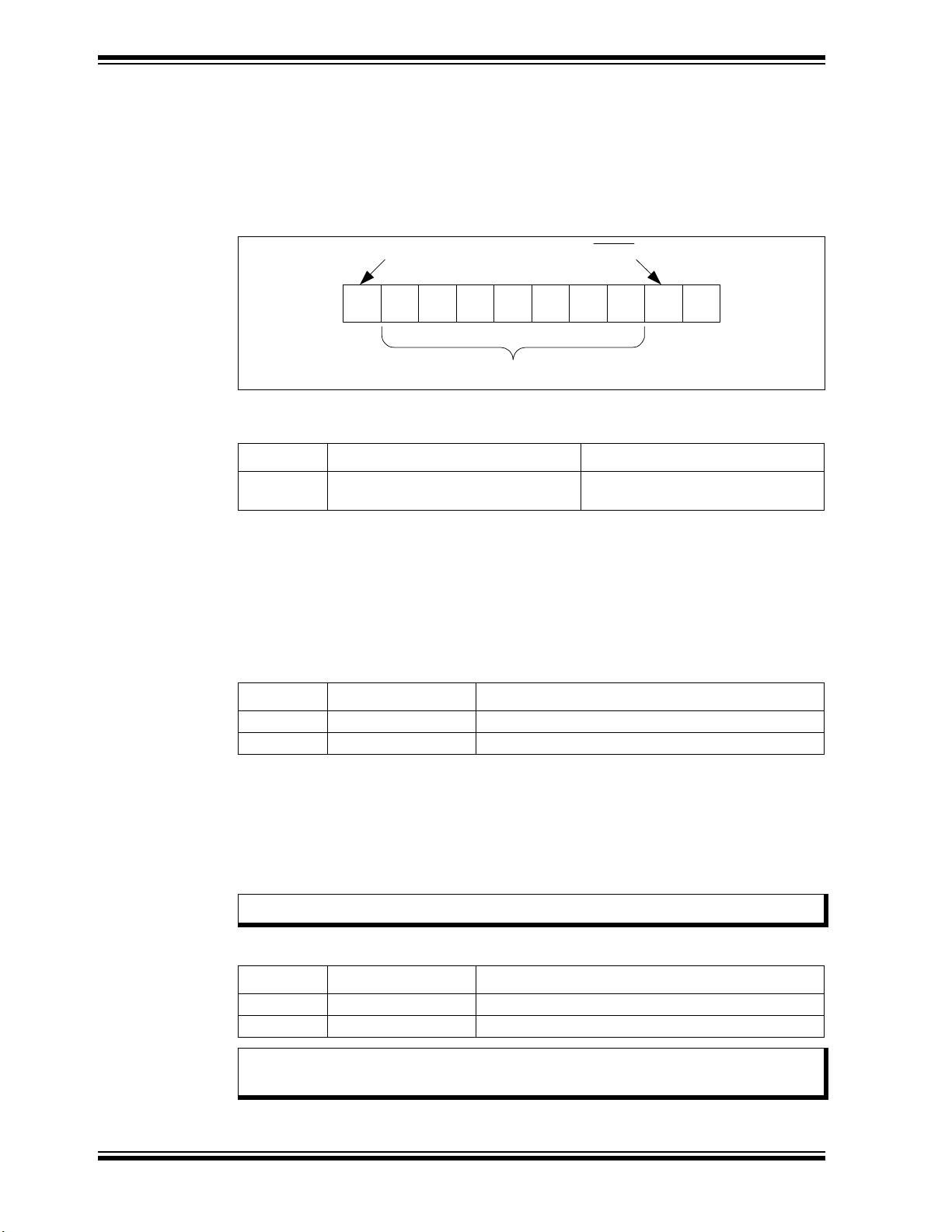
The EVB-LAN9252-DIG-IO utilizes 0x50 (7-bit) I2C slave addressing. The SW3 switch
can be used to select the A0, A1, and A2 address bits, as shown in Figure 2-2 and
Table 2-11. The eighth bit of the slave address determines if the master device wants
to read or write to the EEPROM (24C512).
FIGURE 2-2: SLAVE ADDRESS ALLOCATION
TABLE 2-11: EEPROM SWITCH
Switch Description Settings
SW3 I2C EEPROM address selection switch
(A0, A1, A2). See Figure 2-2.
ON for logic 0 (default)
OFF for logic 1
2.4.4 DIG INPUT Mode
The DIG INPUT Mode can be selected through the headers J10 and J11:
• Logic 1 : (Default) SW4 & SW5 Off position. DIG I/P 0 to 15 tied to pull-up (R98 to
R113)
• Logic 0 : The respective knob of 2-way, 8-position dip switch (SW4 & SW5) need
to be moved to ON side. Signals can be selected individually.
TABLE 2-12: DIGITAL I/O INPUT MODE SELECTION
Header Description Short Pins
J10 Digital Input 0 to 7 1&2, 4&5, 7&8, 10&11, 13&14, 16&17, 19&20, 22&23
J11 Digital Input 8 to 15 1&2, 4&5, 7&8, 10&11, 13&14, 16&17, 19&20, 22&23
2.4.5 DIG OUTPUT Mode
The DIG OUTPUT Mode can be selected through the headers J10 and J11. The
updated Digital I/O values can be seen on the LEDs (D6 to D21):
• Logic 1 : LED illuminated
• Logic 0 : LED not illuminated.
Note: LED (D6 to D21) anode connected to ASIC.
TABLE 2-13: DIGITAL I/O OUTPUT MODE SELECTION (DEFAULT MODE)
Header Description Short Pins
J10 Digital I/O 0 to 7 2&3, 5&6, 8&9, 11&12, 14&15, 17&18, 20&21, 23&24
J11 Digital I/O 8 to 15 2&3, 5&6, 8&9, 11&12, 14&15, 17&18, 20&21, 23&24
Note: The control signal OE_EXT should be connected high by shorting J12 pins
DS50002332A-page 18 Preliminary 2014 Microchip Technology Inc.
15 and 16.
Page 19
Board Details & Configuration
2.4.6 DIG Bidirectional Mode
The DIG Bidirectional Mode can be selected by shorting the respective test point pins
with the headers J10 and J11, as detailed in Table 2-14. The input and output signal
states in this mode are the same as detailed in Section 2.4.4 “DIG INPUT Mode” and
Section 2.4.5 “DIG OUTPUT Mode”.
TABLE 2-14: DIGITAL I/O BIDIRECTIONAL MODE DESCRIPTION
Description Short Pins
Digital I/O 0 to 7 TP5 & J10.1, TP6 & J10.4, TP7 & J10.7, TP8 & J10.10 TP9 & J10.13,
TP10 & J10.16, TP11 & J10.19, TP12 & J10.22, TP13&J10.3,
TP14&J10.6, TP15&J10.9, TP16& J10.12, TP17&J10.15,
TP18&J10.18, TP19& J10.21, TP20&J10.24
Digital I/O 8 to 15 TP21 & J11.1, TP22 & J11.4, TP23 & J11.7, TP24 & J11.10, TP25 &
J11.13, TP26 & J11.16, TP27 & J11.19, TP28 & J11.22, TP29&J11.3,
TP30&J11.6, TP31&J11.9, TP32& J11.12, TP33&J11.15,
TP34&J11.18,TP35& J11.21, TP36&J11.24
2.4.7 Control Signals
All control signals can be probed and controlled via the J12 header, as shown in
Table 2-15.
TABLE 2-15: J12 HEADER CONTROL SIGNAL MAPPING
J12 Pin Number J12 Signal J12 Pin Number J12 Signal
13V323V3
3WD_STATE4 GND
5EOF6GND
7SOF8GND
9LATCH010 GND
11 LATCH1 12 GND
13 WD_TRIG 14 GND
15 OE_EXIT 16 3V3
17 OUTVALID 18 GND
19 LATCH_IN 20 GND
Note: J12 pins 15 & 16 must be shorted in output mode.
2.4.7.1 WD_STATE
This pin is the SyncManager Watchdog State output. A “0” indicates the watchdog has
expired. The state of this signal can be seen in the LED D22.
Note: This signal is not driven (high impedance) until the EEPROM is loaded.
2.4.7.2 LATCH_IN
This pin is the external data latch signal. The input data is sampled each time a rising
edge of LATCH_IN is recognized. By default, this signals is pulled high through
R131and can be made low using switch SW6.
2014 Microchip Technology Inc. Preliminary DS50002332A-page 19
Page 20
EVB-LAN9252-DIG-IO EtherCAT® DIG I/O User’s Guide
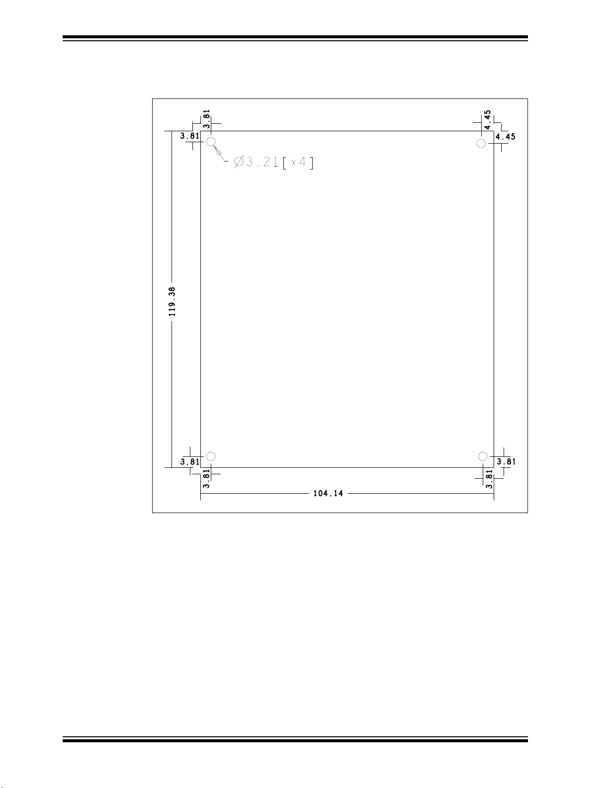
2.5 MECHANICALS
FIGURE 2-3: EVB-LAN9252-DIG-IO MECHANICAL DIMENSIONS
DS50002332A-page 20 Preliminary 2014 Microchip Technology Inc.
Page 21
Chapter 3. LAN9252 EEPROM Programming
3.1 PROGRAMMING THE LAN9252 EEPROM
The LAN9252 configures itself to the desired mode (SPI, 6 HBI modes) by reading the
strap settings located in EEPROM. The LAN9252 EEPROM is programmed and validated via the TwinCAT master tool. The programming procedure is as follows:
Note 1: This example utilizes the TwinCAT tool. Procedures may differ when using
other EtherCAT® master tools.
2: Ensure the system network properties are configured properly for the Eth-
erCAT® frames, Ethernet cable linking your system, and EtherCAT® slave
board.
1. Load the corresponding ESI file in the directory path “C:\TwinCAT\Io\EtherCAT”.
For this demo, the ESI file for the 16-Bit Multiplexed Single-Phase Mode is used.
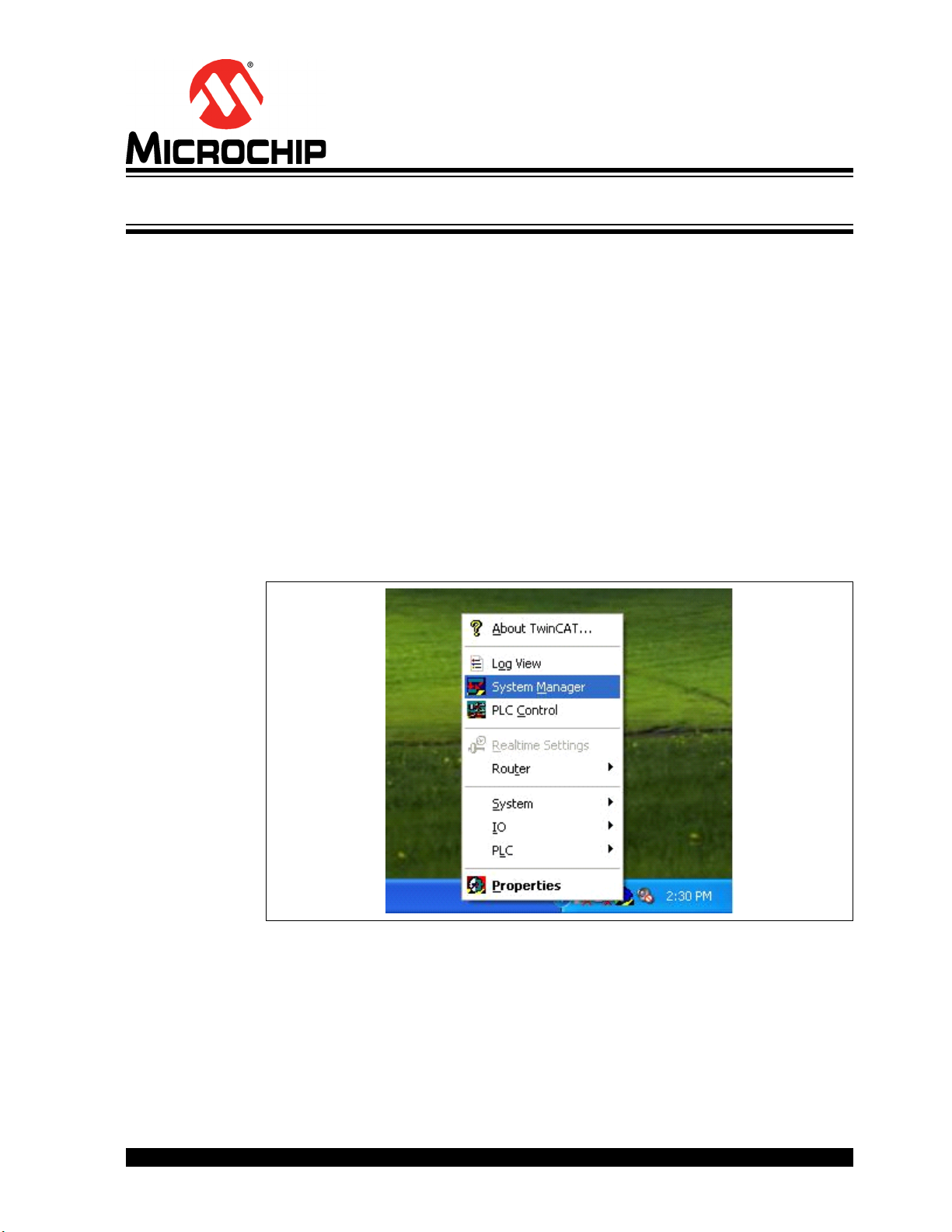
2. If TwinCAT installed successfully, a TwinCAT icon will be shown in the bottom-right corner of the desktop. After clicking the icon, a pop-up list will display.
Select “System Manager”, as shown in Figure 3-1.
EVB-LAN9252-DIG-IO
ETHERCAT® DIG I/O
USER’S GUIDE
FIGURE 3-1: TWINCAT SYSTEM MANAGER
2014 Microchip Technology Inc. Preliminary DS50002332A-page 21
Page 22
EVB-LAN9252-DIG-IO EtherCAT® DIG I/O User’s Guide
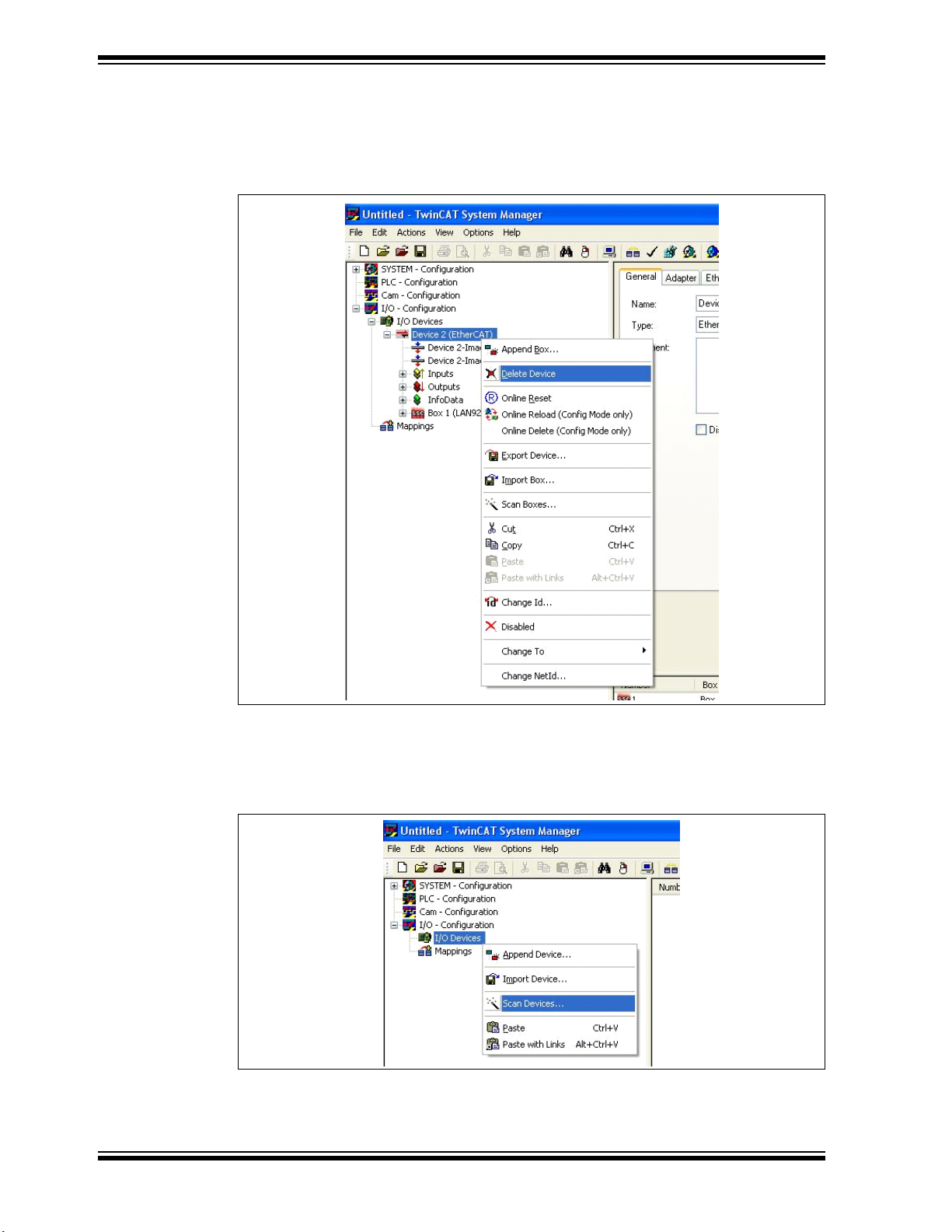
3. If any devices are present, delete them accordingly by clicking the device and
selecting “Delete Device”, as shown in Figure 3-2.
FIGURE 3-2: TWINCAT DELETE DEVICE
4. Scan for EtherCAT® slave devices by clicking “I/O devices” and selecting “Scan
Devices”, as shown in Figure 3-3.
FIGURE 3-3: TWINCAT SCAN DEVICES
DS50002332A-page 22 Preliminary 2014 Microchip Technology Inc.
Page 23
LAN9252 EEPROM Programming
5. After scanning is complete, the right panel of the TwinCAT window will appear as
shown in Figure 3-4.
FIGURE 3-4: TWINCAT DEVICE LIST
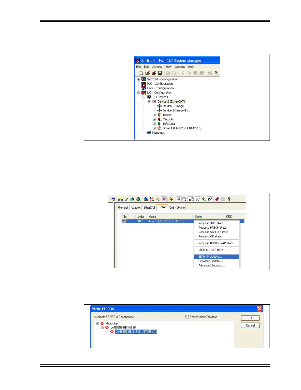
6. After a successful scan, click the “Device 2 (EtherCAT)” drop down bar on the left
panel of the TwinCAT tool (as highlighted in Figure 3-4). Then click the “Online”
tab on the right-side panel of the TwinCAT tool, as shown in Figure 3-5. Right
click the LAN9252 listing and select “EEPROM Update” from the contextual
menu.
FIGURE 3-5: TWINCAT EEPROM UPDATE
7. Upon selecting “EEPROM Update”, the Write EEPROM window will open. Click
the “OK” button to initiate EEPROM programming.
FIGURE 3-6: TWINCAT WRITE EEPROM
2014 Microchip Technology Inc. Preliminary DS50002332A-page 23
Page 24
EVB-LAN9252-DIG-IO
ETHERCAT® DIG I/O
USER’S GUIDE
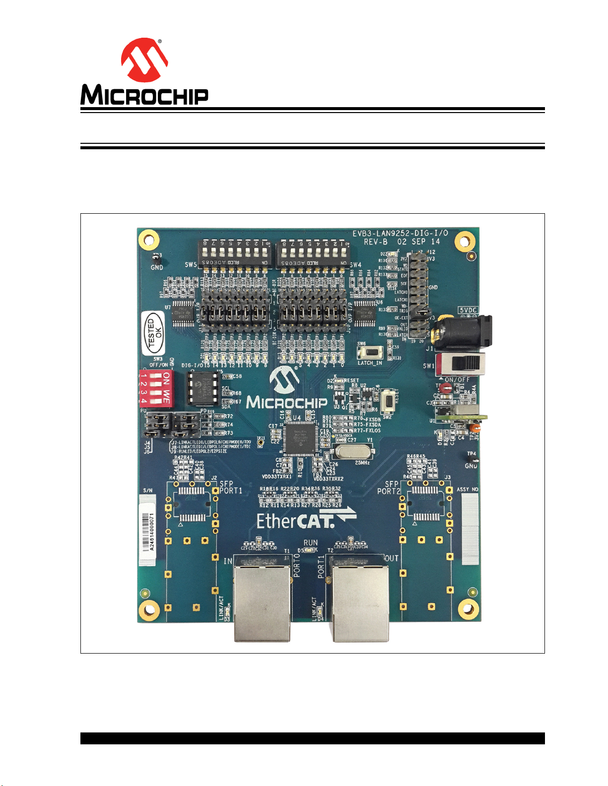
Appendix A. EVB-LAN9252-DIG-IO Evaluation Board
A.1 INTRODUCTION
This appendix shows the EVB-LAN9252-DIG-IO Evaluation Board.
FIGURE A-1: EVB-LAN9252-DIG-IO EVALUATION BOARD
2014 Microchip Technology Inc. Preliminary DS50002332A-page 24
Page 25

EVB-LAN9252-DIG-IO
ETHERCAT® DIG I/O
USER’S GUIDE
Appendix B. EVB-LAN9252-DIG-IO Evaluation Board
Schematics
B.1 INTRODUCTION
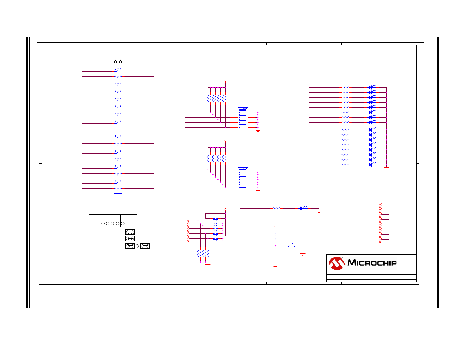
This appendix shows the EVB-LAN9252-DIG-IO Evaluation Board Schematics.
2014 Microchip Technology Inc. Preliminary DS50002332A-page 25
Page 26

DS50002332A-page 26 Preliminary 2014 Microchip Technology Inc.
5
5
4
4
3
3
2
2
1
1
D D
C C
B B
A A
Reset Generator
POWER SUPPLY
(Rb)
(Ra)
OKR-T/3-W12-C
3 V REGULATOR, 3A
( 3V3 fixed when Rb=470E)
"3V3 Present"
Note:
1.POR -> Reset to ASIC & SOC (Default)
2.RESET O/P from ASIC -> Reset to EX-PH Y (PORT2) & SOC :Only Ethercat sku
3.RESET from SOC (GPIO/RST-O/P) -> Reset to ASIC
4.RESET from Push Botton -> Reset to ASIC & SOC
"Reset"
RESET Options
5V_SW
EN12_1
VOUT_3V3
5V_EXT
3V3
3V3
5V
3V3
3V3
3V3
3V3
RST#
Size:
Part Number:
Rev
Date:
Sheet
of
Chennai
India
Project
Name:
Page:
Name:
Board
LAN9252-DIG-IO-EVB
B
B
39
Tuesday, October 21, 2014
LAN9252-DIG-IO-EVB
Power Supply & RST
EVB3-9252-DIG-I/O-RevB
Size:
Part Number:
Rev
Date:
Sheet
of
Chennai
India
Project
Name:
Page:
Name:
Board
LAN9252-DIG-IO-EVB
B
B
39
Tuesday, October 21, 2014
LAN9252-DIG-IO-EVB
Power Supply & RST
EVB3-9252-DIG-I/O-RevB
Size:
Part Number:
Rev
Date:
Sheet
of
Chennai
India
Project
Name:
Page:
Name:
Board
LAN9252-DIG-IO-EVB
B
B
39
Tuesday, October 21, 2014
LAN9252-DIG-IO-EVB
Power Supply & RST
EVB3-9252-DIG-I/O-RevB
U2
TPS3125
SOT23_5
Threshold = 2.64V
Delay = 180ms
RESET#
1
GND
2
RESET
3
MR#
4
VDD
5
TP2
ORANGE
D2
RED
1
A2C
Q1
NDS355AN_NMOS
1
G
3
S
2
D
C5
0.1uF
R5
4.75K
1%
U1
3_Amp
GND
3
VIN
2
ENABLE1TRIM
5
VOUT
4
J1
1
2
3
D1
GRN
1
A
2
C
R1 0E
R2
1K
C6
0.1uF
TP3
BLACK
FB1
2A/0.05DCR
R4A
33E
1%
C2
10uF
25V
C1
4.7uF
DNP
R3
3.30K
1%
TP1
RED
R6
10.0K
1/10W
1%
12
C4
10uF
SW2
sw_pb_2P
R7
100
1/10W
1%
1 2
R8 1K
TP4
BLACK
C3
0.1uF
R9 2.2K
U3
74LVC1G14
2 4
53
1
SW1
P/N:1101M2S3CQE2
Switch, SPDT, Slide
2
3
1
R4
470E
1%
FIGURE B-1: EVB-LAN9252-DIG-IO SCHEMATIC POWER SUPPLY & RESET
EVB-LAN9252-DIG-IO EtherCAT® DIG I/O User’s Guide
Page 27

2014 Microchip Technology Inc. Preliminary DS50002332A-page 27
5
5
4
4
3
3
2
2
1
1
D D
C C
B B
A A
Note:
OSCVSS need to connect to Chip gnd.
Power Supply Filtering
Low ESR
IRQ
REG_EN
RBIAS
VDD12TX1
VDD12TX2
VDD12TX2
VDD12TX1
OSCO
OSCI
3V3
VDD33TXRX1
VDD33TXRX2
VDDCR
VDD33TXRX1
VDD33TXRX2
3V3
3V3
3V3 3V3
3V3
VDDCR
FXSDA/FXLOSA
ATEST/FXLOSEN
RXPA
RXNA
TXNA
TXPA
TXNB
TXPB
RXNB
RXPB
FXSDB/FXLOSB
GPIO0
GPIO1
GPIO2
I2C2_SCL
I2C2_SDA
RST#
Size:
Part Number:
Rev
Date:
Sheet
of
Chennai
India
Project
Name:
Page:
Name:
Board
LAN9252-DIG-IO-EVB
B
B
49
Tuesday, October 21, 2014
LAN9252-DIG-IO-EVB
LAN9252 (Part1)
EVB3-9252-DIG-I/O-RevB
Size:
Part Number:
Rev
Date:
Sheet
of
Chennai
India
Project
Name:
Page:
Name:
Board
LAN9252-DIG-IO-EVB
B
B
49
Tuesday, October 21, 2014
LAN9252-DIG-IO-EVB
LAN9252 (Part1)
EVB3-9252-DIG-I/O-RevB
Size:
Part Number:
Rev
Date:
Sheet
of
Chennai
India
Project
Name:
Page:
Name:
Board
LAN9252-DIG-IO-EVB
B
B
49
Tuesday, October 21, 2014
LAN9252-DIG-IO-EVB
LAN9252 (Part1)
EVB3-9252-DIG-I/O-RevB
C15
0.1uF
C26 18pF
C12
1.0uF DNP
FB3
2A/0.05DCR
C25
0.1uF
C13
0.1uF
C10
0.1uF
C210.1uF
C180.1uF
C23
1.0uF
DNP
C11
0.1uF
C27 18pF
FB4
2A/0.05DCR
BLM18EG221SN1D
POWER
INT PORT0INT PORT1
OSC
I2C
OTHER
SIGNALS
GPIO
(Only for
Lan9252)
U4A
LAN9252
FXSDENA/FXSDA/FXLOSA
9
FXSDENB/FXSDB/FXLOSB
10
VDD33TXRX1
51
TXNA
52
TXPA
53
RXNA
54
RXPA
55
VDD12TX1
56
RBIAS
57
VDD33BIAS
58
VDD12TX2
59
RXPB
60
RXNB
61
TXPB
62
TXNB
63
VDD33TXRX2
64
OSCI
1
OSCO
2
OSCVDD12
3
OSCVSS
4
REG_EN
7
ATEST/FXLOSEN
8
RST#
11
IRQ
44
TESTMODE
41
I2CSCL/EESCL/TCK
43
I2CSDA/EESDA/TMS
42
LINKACTLED0/TDO/LEDPOL0/CHIP_MODE0
48
LINKACTLED1/TDI/LEDPOL1/CHIP_MODE1
46
RUNLED/LEDPOL2/E2PSIZE
45
VDD33
5
VDDIO114VDDIO220VDDIO332VDDIO437VDDIO5
47
VDDCR16VDDCR224VDDCR3
38
GND
65
C220.1uF
C9
1.0uF
DNP
C14
0.1uF
C24
0.1uF
TP71
WHITE
DNP
C16
0.1uF
C20470pF
FB2
2A/0.05DCR
R10 12.1K
1%
Y1
25.000MHz
25ppm
1 2
C7
1.0uF
DNP
FB5
2A/0.05DCR
BLM18EG221SN1D
C17
0.1uF
TP72
SMT
C19
1uF
C8
0.1uF
FIGURE B-2: EVB-LAN9252-DIG-IO SCHEMATIC LAN9252 PT1
EVB-LAN9252-DIG-IO Evaluation Board Schematics
Page 28

DS50002332A-page 28 Preliminary 2014 Microchip Technology Inc.
5
5
4
4
3
3
2
2
1
1
D D
C C
B B
A A
Note:
Capacitors C28 through C31 are optional for EMI purposes
and are not populated on the LAN9252 evaluation board.
These capacitor s are required for op eration in an EMI
constrained environment.
Note:
Capacitors C33 through C36 are optional for EMI purposes
and are not populated on the LAN9252 evaluation board.
These capacitor s are required for op eration in an EMI
constrained environment.
PORT0
PORT1
COP-RXPA
COP-TXNA
COP-RXNA
COP-TXPA
COP-RXPB
COP-TXNB
COP-RXNB
COP-TXPB
VDD33TXRX2
VDD33TXRX1
FX_SFP-RXPA
FX_SFP-RXNA
TXPA
TXNA FX_SFP-TXNA
FX_SFP-TXPA
RXPA
RXNA
FX_SFP-RXPB
FX_SFP-RXNB
TXPB
TXNB FX_SFP- TXNB
FX_SFP-TXPB
RXPB
RXNB
Size:
Part Number:
Rev
Date:
Sheet
of
Chennai
India
Project
Name:
Page:
Name:
Board
LAN9252-DIG-IO-EVB
B
B
59
Tuesday, October 21, 2014
LAN9252-DIG-IO-EVB
Copper Mode Interface
EVB3-9252-DIG-I/O-RevB
Size:
Part Number:
Rev
Date:
Sheet
of
Chennai
India
Project
Name:
Page:
Name:
Board
LAN9252-DIG-IO-EVB
B
B
59
Tuesday, October 21, 2014
LAN9252-DIG-IO-EVB
Copper Mode Interface
EVB3-9252-DIG-I/O-RevB
Size:
Part Number:
Rev
Date:
Sheet
of
Chennai
India
Project
Name:
Page:
Name:
Board
LAN9252-DIG-IO-EVB
B
B
59
Tuesday, October 21, 2014
LAN9252-DIG-IO-EVB
Copper Mode Interface
EVB3-9252-DIG-I/O-RevB
R17 0E
R35 0
R22 0E
DNP
R33 0
XMIT
RCV
75
75 75
1000 pF
2 kV
RJ45
1
4 & 5
2
3
7 & 8
6
75
GRN
YEL
T1
Pulse J0011D01BNL
RD+
3
RXCT
5
RD-
6
TD+
1
TXCT
4
TD-
2
CHS GND
8
GND13GND114MTG15MTG1
16
NC
7
C
10
A
9
C1
11
A1
12
XMIT
RCV
75
75 75
1000 pF
2 kV
RJ45
1
4 & 5
2
3
7 & 8
6
75
GRN
YEL
T2
Pulse J0011D01BNL
RD+
3
RXCT
5
RD-
6
TD+
1
TXCT
4
TD-
2
CHS GND
8
GND13GND114MTG15MTG1
16
NC
7
C
10
A
9
C1
11
A1
12
C29
10pF
50V
5%
DNP
R23 0E
C36
10pF
50V
5%
DNP
C31
10pF
50V
5%
DNP
R30 0E
DNP
R27
49.9
1/10W
1%
R38 0E
RES1210
R20 0E
DNP
R31 0E
R13
49.9
1/10W
1%
R25
49.9
1/10W
1%
R24 0E
RES1210
C33
10pF
50V
5%
DNP
R21 0E
R11
49.9
1/10W
1%
R36 0E
DNP
R28
49.9
1/10W
1%
C28
10pF
50V
5%
DNP
C35
10pF
50V
5%
DNP
R14
49.9
1/10W
1%
R29
0E
C32
0.022uF
50V
10%
R37 0E
C37
0.022uF
50V
10%
R15
0E
R18 0E
DNP
R16 0E
DNP
C30
10pF
50V
5%
DNP
R26
49.9
1/10W
1%
R12
49.9
1/10W
1%
R34 0E
DNP
C34
10pF
50V
5%
DNP
R19 0
R32 0E
DNP
FIGURE B-3: EVB-LAN9252-DIG-IO SCHEMATIC COPPER MODE INTERFACE
EVB-LAN9252-DIG-IO EtherCAT® DIG I/O User’s Guide
Page 29

2014 Microchip Technology Inc. Preliminary DS50002332A-page 29
5
5
4
4
3
3
2
2
1
1
D D
C C
B B
A A
Fiber Port 0 :SFP Interface
Fiber Port 1 :SFP Interface
Note:Place
capacitors,
and resistors
close to FOT
Note:Place
resistors
close to
ASIC
Note:Place
capacitors,
and resistors
close to FOT
Note:Place
resistors
close to
ASIC
SFP_VCCT
SFP_VCCR
SFP_TD-
SFP_TD+
SFP_RD-
SFP_RD+
SFP_VCCT2
SFP_VCCR2
SFP_TD2-
SFP_TD2+
SFP_RD2-
SFP_RD2+
SFP_VCCT
SFP_VCCT2
3V3
3V3
3V3
3V3
FXSDA/FXLOSA FXSDB/FXLOSB
FX_SFP-TXPA
FX_SFP-RXNA
FX_SFP-RXPA
FX_SFP-TXNA
FX_SFP-RXNB
FX_SFP-RXPB
FX_SFP-TXPB
FX_SFP-TXNB
Size:
Part Number:
Rev
Date:
Sheet
of
Chennai
India
Project
Name:
Page:
Name:
Board
LAN9252-DIG-IO-EVB
B
B
69
Tuesday, October 21, 2014
LAN9252-DIG-IO-EVB
SFP Interface
EVB3-9252-DIG-I/O-RevB
Size:
Part Number:
Rev
Date:
Sheet
of
Chennai
India
Project
Name:
Page:
Name:
Board
LAN9252-DIG-IO-EVB
B
B
69
Tuesday, October 21, 2014
LAN9252-DIG-IO-EVB
SFP Interface
EVB3-9252-DIG-I/O-RevB
Size:
Part Number:
Rev
Date:
Sheet
of
Chennai
India
Project
Name:
Page:
Name:
Board
LAN9252-DIG-IO-EVB
B
B
69
Tuesday, October 21, 2014
LAN9252-DIG-IO-EVB
SFP Interface
EVB3-9252-DIG-I/O-RevB
+
C50
10uF
16V
DNP
C47
0.1uF
R49
130
C42 0.1uF
+
C48
10uF
16V
R56
4.7K
C39 0.1uF
C38 0.1uF
R50
130
L3 1uH
C44 0.1uF
C41 0.1uF
R57
4.7K
C49
0.1uF
+
C56
10uF
16V
R58
4.7K
C43 0.1uF
C40 0.1uF
R48
100
L1 1uH
R45
49.9
R59
4.7K
R41
49.9
C45 0.1uF
R46
49.9
C57
0.1uF
R42
49.9
R53
4.7K
L4 1uH
R54
4.7K
+
C52
10uF
16V
R44
82
R55
4.7K
R47
100
+
C54
10uF
16V
J3
FTLF1217P2
VeeT1TXFault2TX Disable3MOD-DEF(2)4MOD-DEF (1)5MOD-DEF (0)6Rate Select7LOS8VeeR9VeeR1
10
VeeR311VeeR2
14
RD-
12
RD+
13
VccR
15
VccT
16
VeeT2
17
TD+
18
TD-
19
VeeT1
20
21
21
22
22
23
23
24
24
25
25
26
26
27
27
28
28
29
29
30
30
31
31
C51
0.1uF
R43
82
L2 1uH
R60
4.7K
J2
FTLF1217P2
VeeT1TXFault2TX Disable3MOD-DEF(2)4MOD-DEF (1)5MOD-DEF (0)6Rate Select7LOS8VeeR9VeeR1
10
VeeR311VeeR2
14
RD-
12
RD+
13
VccR
15
VccT
16
VeeT2
17
TD+
18
TD-
19
VeeT1
20
21
21
22
22
23
23
24
24
25
25
26
26
27
27
28
28
29
29
30
30
31
31
R51
130
C53
0.1uF
C55
0.1uF
R40
82
+
C46
10uF
16V
DNP
R52
130
R39
82
FIGURE B-4: EVB-LAN9252-DIG-IO SCHEMATIC SFP INTERFACE
EVB-LAN9252-DIG-IO Evaluation Board Schematics
Page 30

DS50002332A-page 30 Preliminary 2014 Microchip Technology Inc.
5
5
4
4
3
3
2
2
1
1
D D
C C
B B
A A
GPIO [0:2] & LED_POL_Strap
LINK/ACT for PORT0
6LJQDOV)XQFWLRQV
*3,2 /,1.$&7/('7'2/('32/&+,3B02'(
*3,2 /,1.$&7/('7',/('32/&+,3B02'(
*3,2 581/('/('32/(36,=(
Note:
--To use GPIOs as LED
* Short 2-3 of both jumpers (ex. for GPIO0 short 2-3 of J4 & J7)
7KH/('LVVHWDVDFWLYHORZ
&+,3B02'(
7KH/('LVVHWDVDFWLYHKLJK
&+,3B02'(
6LJQDO1DPH
&RQQHFWRU
--
/RJLF
(36,=(
--
--
--
--
--
7KH/('LVVHWDVDFWLYHORZ
7KH/('LVVHWDVDFWLYHKLJK
7KH/('LVVHWDVDFWLYHORZ
((35206L]H .ELWV.[WKURXJK.ELWV.[RU0ELWV.[/$1RQO\
7KH/('LVVHWDVDFWLYHKLJK
((35206L]H .ELWV[WKURXJK.ELWV.[
Strap Details
I2C EEPROM
TH IC.
Different sizes can be mounted
I2C EEPROM Lower size
Below 16K(2K X 8) (24FC04)
I2C EEPROM Higher size
Above 16K(2K X 8) (24FC512 )
FX_Los_Strap_1 & 2
FX_Mode_Strap_1 & 2
5 5
5HI9ROWDJH )XQFWLRQ
3RXSXODWH
'13
9
$ERYH9VHOHFWV);/26IRUSRUWVDQG
3RXSXODWH 3RXSXODWH 9
/HYHORI9VHOHFWV);/26IRUSRUWDQG
);6'FRSSHUWZLVWHGSDLUIRUSRUW
IXUWKHUGHWHUPLQHGE\);6'%
3RXSXODWH
'HIDXOW
'13
'HIDXOW
'HIDXOW
/HYHORI96HOHFWV);6'FRSSHUWZLVWHGSDLU
IRUSRUWV$DQG%
IXUWKHUGHWHUPLQHGE\);6'$DQG);6'%
LINK/ACT for PORT1
RUNLED
/('3RODULW\6WUDS
&+,3B02'(>@
3RUW'HVFULSWLRQ
>'HIDXOW@
325702'(
5(6(59('
3257
'2:1675($002'(
3RUW 3+<$
3RUW 3+<%
5(6(59('
3RUW 3+<$
3RUW 3+<%
3RUW 0,,
3RUW 0,,
3RUW 3+<%
3RUW 3+<$
3257
83675($002'(
02'(
&+,3B02'(>@6WUDS'HWDLOV
3257
&RSSHU
'HIDXOW
)LEHU
3RXSXODWH
'13
3257
5 5
55
3257
02'(
)LEHU
5 5
5 5
&RSSHU
'HIDXOW
>'HIDXOW@
LED1_CATHODE
GPIO1
GPIO1
LED1_ANODE
LED2_ANODE
LED0_CATHODE
LED2_CATHODE
GPIO0
GPIO0 GPIO2
GPIO2
LED0_ANODE
LED0_ANODE
LED0_CATHODE
LED1_ANODE
LED1_CATHODE
LED2_ANODE
LED2_CATHODE
I2C2_2
I2C2_3
I2C2_7
I2C2_1
3V3
3V3
3V3
3V3
3V3
3V3
3V3 3V3 3V3
GPIO0
GPIO1
GPIO2
I2C2_SDA
I2C2_SCL
ATEST/FXLOSEN
FXSDA/FXLOSA
FXSDB/FXLOSB
Size:
Part Number:
Rev
Date:
Sheet
of
Chennai
India
Project
Name:
Page:
Name:
Board
LAN9252-DIG-IO-EVB
B
B
79
Monday, December 08, 2014
LAN9252-DIG-IO-EVB
STRAP,GPIO,I2C & FXLOS
EVB3-9252-DIG-I/O-RevB
Size:
Part Number:
Rev
Date:
Sheet
of
Chennai
India
Project
Name:
Page:
Name:
Board
LAN9252-DIG-IO-EVB
B
B
79
Monday, December 08, 2014
LAN9252-DIG-IO-EVB
STRAP,GPIO,I2C & FXLOS
EVB3-9252-DIG-I/O-RevB
Size:
Part Number:
Rev
Date:
Sheet
of
Chennai
India
Project
Name:
Page:
Name:
Board
LAN9252-DIG-IO-EVB
B
B
79
Monday, December 08, 2014
LAN9252-DIG-IO-EVB
STRAP,GPIO,I2C & FXLOS
EVB3-9252-DIG-I/O-RevB
R634.7K
J7
123
D4
GRN
1
A2C
R78 10K
DNP
R71
10.0K
12
R74
1K
R76 10K
R77
10K
DNP
J5
123
C58
0.1uF
R672K
J8
123
R654.7K
R73
1K
R75 10K
DNP
D3
GRN
1
A2C
SW3
SW DIP-4/SM
1
2
3
4
8
7
6
5
J4
123
U5
24FC512
GND
4
VCC
8
SDA
5
SCL
6
A0
1
A1
2
A2
3
WP
7
R80 10K
R72
1K
R70
10.0K
12
R644.7K
J6
123
R69
10.0K
12
R664.7K
J9
123
R79
10K
D5
GRN
1
A2C
R682K
FIGURE B-5: EVB-LAN9252-DIG-IO SCHEMATIC STRAP, GPIO, I2C & FXLOS
EVB-LAN9252-DIG-IO EtherCAT® DIG I/O User’s Guide
Page 31

2014 Microchip Technology Inc. Preliminary DS50002332A-page 31
5
5
4
4
3
3
2
2
1
1
D D
C C
B B
A A
DIG-IO
Note: Placement Instruction
Place the TPs in 100 mil distan ce from the respective IN_DIGIOx or OUT_D IGIOx PINS of J10 & J11
Placement should be such a way that, jumpers should be able to
added between the t est points and J10 or J11 connectors
DIGIO0
DIGIO1
DIGIO2
DIGIO3
DIGIO5
DIGIO6
DIGIO7
OUT_BUF_DIGIO0
OUT_BUF_DIGIO1
OUT_BUF_DIGIO2
OUT_BUF_DIGIO3
OUT_BUF_DIGIO4
OUT_BUF_DIGIO5
OUT_BUF_DIGIO6
OUT_BUF_DIGIO7
OUT_BUF_DIGIO14
OUT_BUF_DIGIO15
DIGIO4
DIGIO8
DIGIO9
DIGIO10
DIGIO11
DIGIO13
DIGIO14
DIGIO15
OUTVALID
OUT_BUF_DIGIO8
OUT_BUF_DIGIO9
OUT_BUF_DIGIO10
OUT_BUF_DIGIO11
OUT_BUF_DIGIO12
OUT_BUF_DIGIO13
OUTVALID
DIGIO12
3V3
3V3
3V3
LATCH1
LATCH0
DIGIO0
DIGIO1
DIGIO2
DIGIO3
DIGIO4
DIGIO5
DIGIO6
DIGIO7
DIGIO8
DIGIO9
DIGIO10
DIGIO11
DIGIO13
DIGIO14
DIGIO15
OE_EXT
LATCH_IN
OUTVALID
WD_TRIG
SOF
EOF
WD_STATE
DIGIO12
Size:
Part Number:
Rev
Date:
Sheet
of
Chennai
India
Project
Name:
Page:
Name:
Board
LAN9252-DIG-IO-EVB
B
B
89
Wednesday, October 22, 2014
LAN9252-DIG-IO-EVB
LAN9252-Part2
EVB3-9252-DIG-I/O-RevB
Size:
Part Number:
Rev
Date:
Sheet
of
Chennai
India
Project
Name:
Page:
Name:
Board
LAN9252-DIG-IO-EVB
B
B
89
Wednesday, October 22, 2014
LAN9252-DIG-IO-EVB
LAN9252-Part2
EVB3-9252-DIG-I/O-RevB
Size:
Part Number:
Rev
Date:
Sheet
of
Chennai
India
Project
Name:
Page:
Name:
Board
LAN9252-DIG-IO-EVB
B
B
89
Wednesday, October 22, 2014
LAN9252-DIG-IO-EVB
LAN9252-Part2
EVB3-9252-DIG-I/O-RevB
TP14
TP5
TP29
TP30
TP35
TP19
4.7K R83
U6
74LC245A/SO
A0
2
A1
3
A2
4
A3
5
A4
6
A5
7
A6
8
A7
9
OE
19
DIR
1
B0
18
B1
17
B2
16
B3
15
B4
14
B5
13
B6
12
B7
11
VCC
20
GND
10
TP31
TP6
TP32
TP7
TP12
TP9
4.7K R87
4.7K R84
TP23
TP36
4.7K R81
TP22
4.7K R96
4.7K R91
TP21
TP26
TP15
4.7K R88
4.7K R94
TP17
4.7K R82
4.7K R86
TP16
TP8
4.7K R97
TP11
R89
10K
TP20
TP13
4.7K R92
4.7K R93
4.7K R95
TP24
U4B
LAN9252
SYNC/LATCH1
18
SYNC/LATCH0
34
A4/DIGIO12/GPI12/GPO12/MII_RXD0
27
A3/DIGIO11/GPI11/GPO11/MII_RXDV
26
A2/ALEHI/DIGIO10/GPI10/GPO10/LINKACTLED2/MII_LINKPOL/LEDPOL6
29
A1/ALELO/OE_EXT/MII_CLK25
25
A0/D15/AD15/DIGIO9/GPI9/GPO9/MII_RXER
33
D14/AD14/DIGIO8/GPI8/GPO8/MII_TXD3/TX_SHIFT1
15
D13/AD13/DIGIO7/GPI7/GPO7/MII_TXD2/TX_SHIFT0
16
D12/AD12/DIGIO6/GPI6/GPO6/MI I_TXD1
21
D11/AD11/DIGIO5/GPI5/GPO5/MI I_TXD0
22
D10/AD10/DIGIO4/GPI4/GPO4/MII_TXEN
23
D9/AD9/LATCH_IN/SCK
19
D8/AD8/DIGIO2/GPI2/GPO2/MII_MDIO
40
D7/AD7/DIGIO1/GPI1/GPO1/MII_MDC
39
D6/AD6/DIGIO0/GPI0/GPO0/MII_RXCLK
36
D5/AD5/OUTVALID/SCS#
50
D3/AD3/WD_TRIG/SIO3
35
D2/AD2/SOF/SIO2
12
D1/AD1/EOF/SO/SIO1
13
D0/AD0/WD_STATE/SI/SIO0
17
RD/RD_WR/DIGIO15/GPI15/GPO15/MII_RXD3
31
WR/ENB/DIGIO14/GPI14/GPO14/MII_RXD2
30
CS/DIGIO13/GPI13/GPO13/MII_RXD1
28
D4/AD4/DIGIO3/GPI3/GPO3/MII_LINK
49
TP18
TP28
TP33
U7
74LC245A/SO
A0
2
A1
3
A2
4
A3
5
A4
6
A5
7
A6
8
A7
9
OE
19
DIR
1
B0
18
B1
17
B2
16
B3
15
B4
14
B5
13
B6
12
B7
11
VCC
20
GND
10
TP10
TP27
4.7K R85
TP25
TP34
4.7K R90
FIGURE B-6: EVB-LAN9252-DIG-IO SCHEMATIC LAN9252 PT2
EVB-LAN9252-DIG-IO Evaluation Board Schematics
Page 32
DS50002332A-page 32 Preliminary 2014 Microchip Technology Inc.
5
5
4
4
3
3
2
2
1
1
D D
C C
B B
A A
'HIDXOW
6:6:DUHLQ2))SRVLWLRQ3XOOXSDFWLYH
)RU3XOO'RZQPRYH6:6:WR21SRVLWLRQ
Digital INPUTS
Digital OUTPUTS
LED for WD_STATE
I/P
O/P
1-2 side short of J11 = Input Mode
2-3 side short of J11 = Output Mode
1-2 side short of J10 = Input Mode
2-3 side short of J10 = Output Mode
41 2 3 5
DIG-IO JUMPER OPTIONS
Short 1-2 = Input Mode
Short 2-3 = Output Mode
Short 1-4 & 3-5 = Bidirectional Mode
J10 & J11
TP5 to 12 TP13 to 20
TP21 to 28 TP29 to 36
41 2
12
23
35
IN_DIGIO0
IN_DIGIO1
IN_DIGIO2
IN_DIGIO6
IN_DIGIO3
IN_DIGIO4
IN_DIGIO5
IN_DIGIO7
IN_DIGIO8
IN_DIGIO9
IN_DIGIO10
IN_DIGIO14
IN_DIGIO11
IN_DIGIO12
IN_DIGIO13
IN_DIGIO15
OUT_DIGIO0
OUT_DIGIO1
OUT_DIGIO2
OUT_DIGIO3
OUT_DIGIO4
OUT_DIGIO5
OUT_DIGIO6
OUT_DIGIO7
OUT_DIGIO8
OUT_DIGIO9
OUT_DIGIO10
OUT_DIGIO11
OUT_DIGIO12
OUT_DIGIO13
OUT_DIGIO14
OUT_DIGIO15
IN_DIGIO0
DIGIO0
IN_DIGIO1
DIGIO1
IN_DIGIO2
DIGIO2
IN_DIGIO3
DIGIO3
IN_DIGIO4
DIGIO4
IN_DIGIO5
DIGIO5
IN_DIGIO6
DIGIO6
IN_DIGIO7
DIGIO7
IN_DIGIO8
DIGIO8
IN_DIGIO9
DIGIO9
IN_DIGIO10
DIGIO10
IN_DIGIO11
DIGIO11
IN_DIGIO12
DIGIO12
IN_DIGIO13
DIGIO13
IN_DIGIO14
DIGIO14
IN_DIGIO15
DIGIO15
OUT_DIGIO0
OUT_DIGIO1
OUT_DIGIO2
OUT_DIGIO3
OUT_DIGIO4
OUT_DIGIO5
OUT_DIGIO6
OUT_DIGIO7
OUT_DIGIO8
OUT_DIGIO9
OUT_DIGIO10
OUT_DIGIO11
OUT_DIGIO12
OUT_DIGIO13
OUT_DIGIO14
OUT_DIGIO15
WD_STATE
LATCH_IN
3V3
3V3
3V3
3V3
DIGIO0
DIGIO1
DIGIO2
DIGIO3
DIGIO4
DIGIO5
DIGIO6
DIGIO7
DIGIO8
DIGIO9
DIGIO10
DIGIO11
DIGIO12
DIGIO13
DIGIO14
DIGIO15
OUTVALID
WD_STATE
EOF
SOF
LATCH0
LATCH1
WD_TRIG
OE_EXT
LATCH_IN
Size:
Part Number:
Rev
Date:
Sheet
of
Chennai
India
Project
Name:
Page:
Name:
Board
LAN9252-DIG-IO-EVB
B
B
99
Wednesday, October 22, 2014
LAN9252-DIG-IO-EVB
DIG-I/O
EVB3-9252-DIG-I/O-RevB
Size:
Part Number:
Rev
Date:
Sheet
of
Chennai
India
Project
Name:
Page:
Name:
Board
LAN9252-DIG-IO-EVB
B
B
99
Wednesday, October 22, 2014
LAN9252-DIG-IO-EVB
DIG-I/O
EVB3-9252-DIG-I/O-RevB
Size:
Part Number:
Rev
Date:
Sheet
of
Chennai
India
Project
Name:
Page:
Name:
Board
LAN9252-DIG-IO-EVB
B
B
99
Wednesday, October 22, 2014
LAN9252-DIG-IO-EVB
DIG-I/O
EVB3-9252-DIG-I/O-RevB
R13410K
R13210K
R1231K
J10
HDR_3x8
1 3
4
2
5
6
789
11
13 15
10 12
14
161718
192021
22 24
23
SW5
SW DIP-8
1
2
3
4
5
6
7
8
16
15
14
13
12
11
10
9
R10210K
R1211K
R10710K
R1181K
R9910K
SW6
sw_pb_2P
R10410K
R10510K
R1161K
R1151K
R1291K
R11210K
R10310K
R11010K
R1261K
R1241K
R10610K
R1221K
R13610K
D22
GRN
1
A2C
R10110K
R131
100K
C59
0.1uF
R11110K
R1201K
D21
GRN
1
A2C
D15
GRN
1
A2C
D20
GRN
1
A2C
D14
GRN
1
A2C
D19
GRN
1
A2C
D13
GRN
1
A2C
D18
GRN
1
A2C
D12
GRN
1
A2C
D17
GRN
1
A2C
D16
GRN
1
A2C
R1191K
R13510K
R1171K
R130 1K
D11
GRN
1
A2C
R9810K
D10
GRN
1
A2C
D9
GRN
1
A2C
D8
GRN
1
A2C
J12
1
3 4
2
5 6
7 8
9
11
13
15
10
12
14
16
17 18
19 20
D7
GRN
1
A2C
D6
GRN
1
A2C
R1281K
R1141K
R10810K
R1271K
R10010K
R13310K
SW4
SW DIP-8
1
2
3
4
5
6
7
8
16
15
14
13
12
11
10
9
R1251K
J11
HDR_3x8
1 3
4
2
5
6
789
11
13 15
10 12
14
161718
192021
22 24
23
R11310K
R10910K
FIGURE B-7: EVB-LAN9252-DIG-IO SCHEMATIC DIGITAL I/O
EVB-LAN9252-DIG-IO EtherCAT® DIG I/O User’s Guide
Page 33

EVB-LAN9252-DIG-IO
ETHERCAT® DIG I/O
USER’S GUIDE
Appendix C. Bill of Materials (BOM)
C.1 INTRODUCTION
This appendix includes the EVB-LAN9252-DIG-IO Evaluation Board Bill of Materials (BOM).
2014 Microchip Technology Inc. Preliminary DS50002332A-page 33
Page 34

DS50002332A-page 34 Preliminary 2014 Microchip Technology Inc.
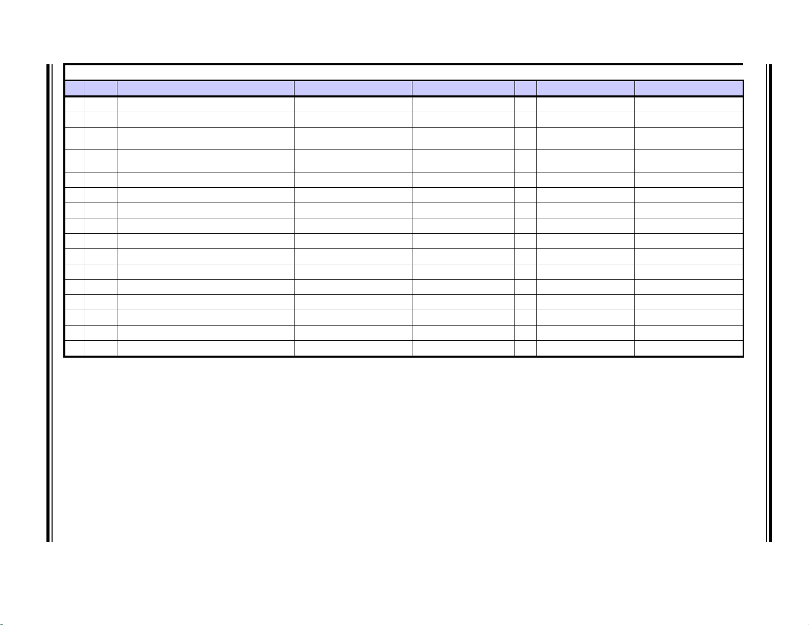
Item Quantity Reference Part PCB Footprint DNP Vender Vender Part NO
12
218
31
41
52
62
721
81
95
10 1
11 6
12 2
13 1
14 1
15 3
16 22
17 1
18 1
19 1
20 1
21 4
22 1
23 1
24 1
25 8
26 8
C2,C4
C3,C5,C6,C8,C10,C11,C13,C14,C15,C16,C17,C18,C21,
C22,C24,C25,C58,C59
C19
C20
C26,C27
C32,C37
D1,D3,D4,D5,D6,D7,D8,D9,D10,D11,D12,D13,D14,D1
5,D16,D17,D18,D19,D20,D21,D22
D2
FB1,FB2,FB3,FB4,FB5
J1
J4,J5,J6,J7,J8,J9
J10,J11
J12
Q1
R1,R15,R29
R2,R8,R72,R73,R74,R114,R115,R116,R117,R118,R119
,R120,R121,R122,R123,R124,R125,R126,
R127,R128,R129,R130
R3
R4
R4A
R5
R6,R69,R70,R71
R7
R9
R10
R11,R12,R13,R14,R25,R26,R27,R28
R17,R19,R21,R23,R31,R33,R35,R37
10uF CAP0805 No Murata GRM21BR61E106KA73L
0.1uF CAP0603 No Murata GRM188R71E104KA01D
1uF CAP0603 No Murata GRM188R61C105KA93D
470pF CAP0603 No Kemet C0603C471K3RACTU
18pF CAP0603 No Murata GRM1885C1H180JA01D
0.022uF CAP0603 No Kemet C0603C223K5RACTU
GRN LED0603 No Wurth electronics 150 060 GS7 500 0
RED LED0603 No Wurth electronics 150 060 RS7 500 0
2A/0.05DCR RES0603 No Murata BLM18EG221SN1D
SKT_PWR_2R0mm_4A_THRU_RA th_conn_pwrjack_dc-210_rt No Cui Stack PJ-002AH
HDR_1x3 TH_CONN_1X3P No FCI 68000-103HLF
HDR_3x8 TH_CONN_3x8P No FCI 68000-108HLF
2x10 TH_CONN_2x10P No FCI 67997-220HLF
NDS355AN_NMOS sot23-NDS No Fairchild NDS355AN
0E RES0603 No Panasonic ERJ-3GEY0R00V
1K RES0603 No Panasonic ERJ-3GEYJ102V
3.30K RES0603 No Yageo America 9C06031A3301FKHFT
470E RES0603 No BOURNS CR0603-FX-4700ELF
33E RES0603 No BOURNS CR0603-FX-33R0ELF
4.75K RES0603 No Panasonic ERJ-3EKF4751V
10.0K RES0603 No Panasonic ERJ-3EKF1002V
100 RES0603 No Panasonic ERJ-3EKF1000V
2.2K RES0603 No Panasonic ERJ-3GEYJ222V
12.1K RES0603 No Rohm MCR01MZPF1202
49.9 RES0603 No Yageo America 9C06031A49R9FKHFT
0E RES0402 No Panasonic ERJ-2GE0R00X
EVB-LAN9252-DIG-IO EtherCAT® DIG I/O User’s Guide
Page 35

DS50002332A-page 35 Preliminary 2014 Microchip Technology Inc.
27 2
28 2
29 25
30 1
31 20
32 1
33 2
34 1
35 2
36 1
37 1
38 2
39 32
40 2
41 1
42 1
43 1
44 1
45 1
46 2
47 1
R24,R38
R67,R68
R76,R79,R80,R89,R98,R99,R100,R101,R102,R103,R10
4,R105,R106,R107,R108,R109,R110,R111,R112,R113,
R132,R133,R134,R135,R136
R131
R81,R82,R83,R84,R85,R86,R87,R88,R90,R91,
R92,R93,R94,R95,R96,R97,R63,R64,R65,R66
SW1
SW2,SW6
SW3
SW4,SW5
TP1
TP2
TP3,TP4
TP5,TP6,TP7,TP8,TP9,TP10,TP11,TP12,TP13,TP14,TP1
5,TP16,TP17,TP18,TP19,TP20,TP21,TP22,
TP23,TP24,TP25,TP26,TP27,TP28,TP29,TP30,
T1,T2
U1
U2
U3
U4
U5
U6,U7
Y1
EVB-LAN9252-DIG-IO EtherCAT® DIG I/O User’s Guide
0E RES1210 No Vishay CRCW12100000Z0EA
2K RES0603 No Panasonic ERJ-3GEYJ202V
10K RES0603 No Panasonic ERJ-3GEYJ103V
100K RES0603 No Panasonic ERJ-3EKF1003V
4.7K RES0603 No Panasonic ERJ-3EKF4701V
SW-SPDT-SLIDE sw_ck_1101m2s3cqe2 No C&K 1101M2S3CQE2
sw_pb_2P sw_pb_2P No Panasonic EVQ-PJU04K
SW DIP-4/SM TH_SW_DIP4 No Wurth electronics 418117270904
SW DIP-8 SW_DIP_SMT_8P-ade08s04 No TE 1-1825058-9/ade08s04
RED TH_TP_60D40 No Keystone 5000
ORANGE TH_TP_60D40 No Keystone 5003
BLACK TH_TP_60D40 No Keystone 5001
WHITE TH_TP No FCI 68000-101HLF
Pulse - J0011D01BNL th_conn_pulse_rj45_j0026 No Pulse Electronics J0011D01BNL
3_Amp TH_DC-DC_VERT_5PIN_P67 No Murata OKR-T/3-W12-C
TPS3125 SOT23_5 No TI TPS3125L30DBVR
74LVC1G14 SOT23_5 No TI SN74L VCIG14DBVR
LAN9252 IC_QFN64 No Microchip LAN9252
24FC512 IC_DIP8_300 No Microchip 24FC512-I/P
74LC245A/SO IC_SO20-MO-153 No TI SN74LVC245APWR
25.000MHz XTAL_HCM49 No Cardinal Components Inc. CSM1Z-A5B2C5-40-25.0D18-F
Page 36
DS50002332A-page 36 Preliminary 2014 Microchip Technology Inc.
Do NOT Populate components:
Item Quantity Reference Part PCB Footprint DNP Vender Vender Part NO
1 1 C1 4.7uF CAP0603 DNP Murata GRM188R60J475KE19D
2 4 C7,C9,C12,C23 1.0uF CAP0603 DNP Murata GRM188R61C105KA93D
3 8 C28,C29,C30,C31,C33,C34,C35,C36 10pF CAP0402 DNP Murata GRM1885C1H100JA01D
414
5 6 C46,C48,C50,C52,C54,C56 10uF CAP_B_3528 DNP Kemet B45190E3106K209
6 2 J2,J3 FTLF1217P2 CONN_FX_SFP_FTLF1217P2 DNP Finisar 775-1011-ND
7 4 L1,L2,L3,L4 1uH L0805 DNP
8 8 R16,R18,R20,R22,R30,R32,R34,R36 0 RES0402 DNP
9 4 R39,R40,R43,R44 82 RES0603 DNP Panasonic ERJ-3EKF1300V
10 4 R41,R42,R45,R46 49.9 RES0603 DNP Yageo America 9C06031A49R9FKHFT
11 2 R47,R48 100 RES0603 DNP Panasonic ERJ-3EKF1000V
12 4 R49,R50,R51,R52 130 RES0603 DNP Panasonic ERJ-3EKF1300V
13 8 R53,R54,R55,R56,R57,R58,R59,R60 4.7K RES0603 DNP Panasonic ERJ-3EKF4701V
14 3 R75,R77,R78 10K RES0603 DNP Panasonic ERJ-3GEYJ103V
15 1 TP71 WHITE TH_TP_60D40 DNP Keystone 5002
16 1 TP72 SMT tp-smd40 DNP NA NA
C38,C39,C40,C41,C42,C43,C44,C45,C47,C49,
C51,C53,C55,C57
0.1uF CAP0603 DNP Murata GRM188R71E104KA01D
EVB-LAN9252-DIG-IO EtherCAT® DIG I/O User’s Guide
Page 37

Worldwide Sales and Service
AMERICAS
Corporate Office
2355 West Chandler Blvd.
Chandler, AZ 85224-6199
Tel: 480-792-7200
Fax: 480-792-7277
Technical Support:
http://www.microchip.com/
support
Web Address:
www.microchip.com
Atlanta
Duluth, GA
Tel: 678-957-9614
Fax: 678-957-1455
Austin, TX
Tel: 512-257-3370
Boston
Westborough, MA
Tel: 774-760-0087
Fax: 774-760-0088
Chicago
Itasca, IL
Tel: 630-285-0071
Fax: 630-285-0075
Cleveland
Independence, OH
Tel: 216-447-0464
Fax: 216-447-0643
Dallas
Addison, TX
Tel: 972-818-7423
Fax: 972-818-2924
Detroit
Novi, MI
Tel: 248-848-4000
Houston, TX
Tel: 281-894-5983
Indianapolis
Noblesville, IN
Tel: 317-773-8323
Fax: 317-773-5453
Los Angeles
Mission Viejo, CA
Tel: 949-462-9523
Fax: 949-462-9608
New York, NY
Tel: 631-435-6000
San Jose, CA
Tel: 408-735-9110
Canada - Toronto
Tel: 905-673-0699
Fax: 905-673-6509
ASIA/PACIFIC
Asia Pacific Office
Suites 3707-14, 37th Floor
Tower 6, The Gateway
Harbour City, Kowloon
Hong Kong
Tel: 852-2943-5100
Fax: 852-2401-3431
Australia - Sydney
Tel: 61-2-9868-6733
Fax: 61-2-9868-6755
China - Beijing
Tel: 86-10-8569-7000
Fax: 86-10-8528-2104
China - Chengdu
Tel: 86-28-8665-5511
Fax: 86-28-8665-7889
China - Chongqing
Tel: 86-23-8980-9588
Fax: 86-23-8980-9500
China - Hangzhou
Tel: 86-571-8792-8115
Fax: 86-571-8792-8116
China - Hong Kong SAR
Tel: 852-2943-5100
Fax: 852-2401-3431
China - Nanjing
Tel: 86-25-8473-2460
Fax: 86-25-8473-2470
China - Qingdao
Tel: 86-532-8502-7355
Fax: 86-532-8502-7205
China - Shanghai
Tel: 86-21-5407-5533
Fax: 86-21-5407-5066
China - Shenyang
Tel: 86-24-2334-2829
Fax: 86-24-2334-2393
China - Shenzhen
Tel: 86-755-8864-2200
Fax: 86-755-8203-1760
China - Wuhan
Tel: 86-27-5980-5300
Fax: 86-27-5980-5118
China - Xian
Tel: 86-29-8833-7252
Fax: 86-29-8833-7256
China - Xiamen
Tel: 86-592-2388138
Fax: 86-592-2388130
China - Zhuhai
Tel: 86-756-3210040
Fax: 86-756-3210049
ASIA/PACIFIC
India - Bangalore
Tel: 91-80-3090-4444
Fax: 91-80-3090-4123
India - New Delhi
Tel: 91-11-4160-8631
Fax: 91-11-4160-8632
India - Pune
Tel: 91-20-3019-1500
Japan - Osaka
Tel: 81-6-6152-7160
Fax: 81-6-6152-9310
Japan - Tokyo
Tel: 81-3-6880- 3770
Fax: 81-3-6880-3771
Korea - Daegu
Tel: 82-53-744-4301
Fax: 82-53-744-4302
Korea - Seoul
Tel: 82-2-554-7200
Fax: 82-2-558-5932 or
82-2-558-5934
Malaysia - Kuala Lumpur
Tel: 60-3-6201-9857
Fax: 60-3-6201-9859
Malaysia - Penang
Tel: 60-4-227-8870
Fax: 60-4-227-4068
Philippines - Manila
Tel: 63-2-634-9065
Fax: 63-2-634-9069
Singapore
Tel: 65-6334-8870
Fax: 65-6334-8850
Taiwan - Hsin Chu
Tel: 886-3-5778-366
Fax: 886-3-5770-955
Taiwan - Kaohsiung
Tel: 886-7-213-7830
Taiwan - Taipei
Tel: 886-2-2508-8600
Fax: 886-2-2508-0102
Thailand - Bangkok
Tel: 66-2-694-1351
Fax: 66-2-694-1350
EUROPE
Austria - Wels
Tel: 43-7242-2244-39
Fax: 43-7242-2244-393
Denmark - Copenhagen
Tel: 45-4450-2828
Fax: 45-4485-2829
France - Paris
Tel: 33-1-69-53-63-20
Fax: 33-1-69-30-90-79
Germany - Dusseldorf
Tel: 49-2129-3766400
Germany - Munich
Tel: 49-89-627-144-0
Fax: 49-89-627-144-44
Germany - Pforzheim
Tel: 49-7231-424750
Italy - Milan
Tel: 39-0331-742611
Fax: 39-0331-466781
Italy - Venice
Tel: 39-049-7625286
Netherlands - Drunen
Tel: 31-416-690399
Fax: 31-416-690340
Poland - Warsaw
Tel: 48-22-3325737
Spain - Madrid
Tel: 34-91-708-08-90
Fax: 34-91-708-08-91
Sweden - Stockholm
Tel: 46-8-5090-4654
UK - Wokingham
Tel: 44-118-921-5800
Fax: 44-118-921-5820
03/25/14
DS50002332A-page 37 Preliminary 2014 Microchip Technology Inc.
 Loading...