

Page 1

EVB-LAN9252-3PORT
EtherCAT® ESC
PHY Connection Mode
Evaluation Board
User’s Guide
2015 Microchip Technology Inc. DS50002403A
Page 2

Note the following details of the code protection feature on Microchip devices:
YSTEM
CERTIFIE DBYDNV
== ISO/TS16949==
• Microchip products meet the specification contained in their particular Microchip Data Sheet.
• Microchip believes that its family of products is one of the most secure families of its kind on the market today, when used in the
intended manner and under normal conditions.
• There are dishonest and possibly illegal methods used to breach the code protection feature. All of these methods, to our
knowledge, require using the Microchip products in a manner outside the operating specifications contained in Microchip’s Data
Sheets. Most likely, the person doing so is engaged in theft of intellectual property.
• Microchip is willing to work with the customer who is concerned about the integrity of their code.
• Neither Microchip nor any other semiconductor manufacturer can guarantee the security of their code. Code protection does not
mean that we are guaranteeing the product as “unbreakable.”
Code protection is constantly evolving. We at Microchip are committed to continuously improving the code protection features of our
products. Attempts to break Microchip’s code protection feature may be a violation of the Digital Millennium Copyright Act. If such acts
allow unauthorized access to your software or other copyrighted work, you may have a right to sue for relief under that Act.
Information contained in this publication regarding device applications and the like is provided only for your convenience and may be
superseded by updates. It is your responsibility to ensure that your application meets with your specifications. MICROCHIP MAKES NO
REPRESENTATIONS OR WARRANTIES OF ANY KIND WHETHER EXPRESS OR IMPLIED, WRITTEN OR ORAL, STATUTORY OR
OTHERWISE, RELATED TO THE INFORMATION, INCLUDING BUT NOT LIMITED TO ITS CONDITION, QUALITY, PERFORMANCE,
MERCHANTABILITY OR FITNESS FOR PURPOSE. Microchip disclaims all liability arising from this information and its use. Use of Microchip devices in life support and/or safety applications is entirely at the buyer’s risk, and the buyer agrees to defend, indemnify and hold
harmless Microchip from any and all damages, claims, suits, or expenses resulting from such use. No licenses are conveyed, implicitly or
otherwise, under any Microchip intellectual property rights unless otherwise stated.
Trademarks
The Microchip name and logo, the Microchip logo, dsPIC, FlashFlex, flexPWR, JukeBlox, K
MediaLB, MOST, MOST logo, MPLAB, OptoLyzer, PIC, PICSTART, PIC
UNI/O are registered trademarks of Microchip Technology Incorporated in the U.S.A. and other countries.
The Embedded Control Solutions Company and mTouch are registered trademarks of Microchip Technology Incorporated in the U.S.A.
Analog-for-the-Digital Age, BodyCom, chipKIT, chipKIT logo, CodeGuard, dsPICDEM, dsPICDEM.net, ECAN, In-Circuit Serial
Programming, ICSP, Inter-Chip Connectivity, KleerNet, KleerNet logo, MiWi, motorBench, MPASM, MPF, MPLAB Certified logo,
MPLIB, MPLINK, MultiTRAK, NetDetach, Omniscient Code Generation, PICDEM, PICDEM.net, PICkit, PICtail, RightTouch logo, REAL
ICE, SQI, Serial Quad I/O, Total Endurance, TSHARC, USBCheck, VariSense, ViewSpan, WiperLock, Wireless DNA, and ZENA are
trademarks of Microchip Technology Incorporated in the U.S.A. and other countries.
SQTP is a service mark of Microchip Technology Incorporated in the U.S.A.
Silicon Storage Technology is a registered trademark of Microchip Technology Inc. in other countries.
GestIC is a registered trademark of Microchip Technology Germany II GmbH & Co. KG, a subsidiary of Microchip Technology Inc., in
other countries.
All other trademarks mentioned herein are property of their respective companies.
© 2015, Microchip Technology Incorporated, Printed in the U.S.A., All Rights Reserved.
ISBN: 978-1-63277-752-2
32
logo, RightTouch, SpyNIC, SST, SST Logo, SuperFlash and
EELOQ, KEELOQ logo, Kleer, LANCheck,
QUALITYMANAGEMENTS
DS50002403A-page 2 2015 Microchip Technology Inc.
Microchip received ISO/TS-16949:2009 certification for its worldwide
headquarters, design and wafer fabrication facilities in Chandler and
Tempe, Arizona; Gresham, Oregon and design centers in California
and India. The Company’s quality system processes and procedures
are for its PIC
devices, Serial EEPROMs, microperipherals, nonvolatile memory and
analog products. In addition, Microchip’s quality system for the design
and manufacture of development systems is ISO 9001:2000 certified.
®
MCUs and dsPIC® DSCs, KEELOQ
®
code hopping
Page 3

Object of Declaration: EVB-LAN9252-3PORT
2015 Microchip Technology Inc. DS50002403A-page 3
Page 4

EVB-LAN9252-3PORT EtherCAT® ESC PHY Connection Mode User’s Guide
NOTES:
DS50002403A-page 4 2015 Microchip Technology Inc.
Page 5

EVB-LAN9252-3PORT
ETHERCAT® ESC PHY CONNECTION MODE
USER’S GUIDE
Table of Contents
Preface ........................................................................................................................... 7
Introduction............................................................................................................ 7
Document Layout .................................................................................................. 7
Conventions Used in this Guide ............................................................................ 8
The Microchip Web Site ........................................................................................ 9
Development Systems Customer Change Notification Service ............................ 9
Customer Support ................................................................................................. 9
Document Revision History ................................................................................. 10
Chapter 1. Overview
1.1 Introduction ................................................................................................... 11
1.2 References ................................................................................................... 12
1.3 Terms and Abbreviations ............................................................................. 12
Chapter 2. Board Details
2.1 Power ........................................................................................................... 13
2.2 Resets .......................................................................................................... 13
2.2.1 Power-on Reset ......................................................................................... 13
2.2.2 Reset Out .................................................................................................. 13
2.3 Clock ............................................................................................................ 13
Chapter 3. Board Configuration
3.1 External PHY connection mode ................................................................... 15
3.2 Jumper Settings ........................................................................................... 15
3.2.1 Strap Options ............................................................................................ 16
3.2.2 LED Indicators ........................................................................................... 19
3.2.3 EEPROM Switch ....................................................................................... 19
3.2.4 SPI + 3 Port Mode Selection ..................................................................... 20
3.2.5 SoC ........................................................................................................... 22
3.3 Mechanicals ................................................................................................. 24
Appendix A. EVB-LAN9252-3PORT Evaluation Board
A.1 Introduction .................................................................................................. 25
Appendix B. EVB-LAN9252-3PORT Evaluation Board Schematics
B.1 Introduction .................................................................................................. 27
Appendix C. Bill of Materials (BOM)
C.1 Introduction .................................................................................................. 39
Worldwide Sales and Service .................................................................................... 44
2015 Microchip Technology Inc. DS50002403A-page 5
Page 6

EVB-LAN9252-3PORT EtherCAT® ESC PHY Connection Mode User’s Guide
NOTES:
DS50002403A-page 6 2015 Microchip Technology Inc.
Page 7

EVB-LAN9252-3PORT
ETHERCAT® ESC PHY CONNECTION
MODE USER’S GUIDE
Preface
NOTICE TO CUSTOMERS
All documentation becomes dated, and this manual is no exception. Microchip tools and
documentation are constantly evolving to meet customer needs, so some actual dialogs
and/or tool descriptions may differ from those in this document. Please refer to our web site
(www.microchip.com) to obtain the latest documentation available.
Documents are identified with a “DS” number. This number is located on the bottom of each
page, in front of the page number. The numbering convention for the DS number is
“DSXXXXXA”, where “XXXXX” is the document number and “A” is the revision level of the
document.
For the most up-to-date information on development tools, see the MPLAB
Select the Help menu, and then Topics to open a list of available online help files.
®
IDE online help.
INTRODUCTION
This chapter contains general information that will be useful to know before using the
EVB-LAN9252-3PORT. Items discussed in this chapter include:
• Document Layout
• Conventions Used in this Guide
• The Microchip Web Site
• Development Systems Customer Change Notification Service
• Customer Support
• Document Revision History
DOCUMENT LAYOUT
This document describes how to use the EVB-LAN9252-3PORT as a development tool
for the Microchip LAN9252 EtherCAT
follows:
• Chapter 1. “Overview” – Shows a brief description of the
EVB-LAN9252-3PORT.
• Chapter 2. “Board Details” – Includes details and instructions for using the
EVB-LAN9252-3PORT.
• Chapter 3. “Board Configuration” – Describes the various
EVB-LAN9252-3PORT board features, including jumpers, LEDs, test points, system connections, and switches.
• Appendix A. “EVB-LAN9252-3PORT Evaluation Board” – This appendix
shows the EVB-LAN9252-3PORT.
• Appendix B. “EVB-LAN9252-3PORT Evaluation Board Schematics” – This
appendix shows the EVB-LAN9252-3PORT schematics.
• Appendix C. “Bill of Materials (BOM)” – This appendix includes the
EVB-LAN9252-3PORT Bill of Materials (BOM).
®
slave controller. The manual layout is as
2015 Microchip Technology Inc. DS50002403A-page 7
Page 8

EVB-LAN9252-3PORT EtherCAT® ESC PHY Connection Mode User’s Guide
CONVENTIONS USED IN THIS GUIDE
This manual uses the following documentation conventions:
DOCUMENTATION CONVENTIONS
Description Represents Examples
Arial font:
Italic characters Referenced books MPLAB® IDE User’s Guide
Emphasized text ...is the only compiler...
Initial caps A window the Output window
A dialog the Settings dialog
A menu selection select Enable Programmer
Quotes A field name in a window or
dialog
Underlined, italic text with
right angle bracket
Bold characters A dialog button Click OK
N‘Rnnnn A number in verilog format,
Text in angle brackets < > A key on the keyboard Press <Enter>, <F1>
Courier New font:
Plain Courier New Sample source code #define START
Italic Courier New A variable argument file.o, where file can be
Square brackets [ ] Optional arguments mcc18 [options] file
Curly brackets and pipe
character: { | }
Ellipses... Replaces repeated text var_name [,
A menu path File>Save
A tab Click the Power tab
where N is the total number of
digits, R is the radix and n is a
digit.
Filenames autoexec.bat
File paths c:\mcc18\h
Keywords _asm, _endasm, static
Command-line options -Opa+, -Opa-
Bit values 0, 1
Constants 0xFF, ‘A’
Choice of mutually exclusive
arguments; an OR selection
Represents code supplied by
user
“Save project before build”
4‘b0010, 2‘hF1
any valid filename
[options]
errorlevel {0|1}
var_name...]
void main (void)
{ ...
}
DS50002403A-page 8 2015 Microchip Technology Inc.
Page 9

Preface
THE MICROCHIP WEB SITE
Microchip provides online support via our web site at www.microchip.com. This web
site is used as a means to make files and information easily available to customers.
Accessible by using your favorite Internet browser, the web site contains the following
information:
• Product Support – Data sheets and errata, application notes and sample
programs, design resources, user’s guides and hardware support documents,
latest software releases and archived software
• General Technical Support – Frequently Asked Questions (FAQs), technical
support requests, online discussion groups, Microchip consultant program
member listing
• Business of Microchip – Product selector and ordering guides, latest Microchip
press releases, listing of seminars and events, listings of Microchip sales offices,
distributors and factory representatives
DEVELOPMENT SYSTEMS CUSTOMER CHANGE NOTIFICATION SERVICE
Microchip’s customer notification service helps keep customers current on Microchip
products. Subscribers will receive e-mail notification whenever there are changes,
updates, revisions or errata related to a specified product family or development tool of
interest.
To register, access the Microchip web site at www.microchip.com, click on Customer
Change Notification and follow the registration instructions.
The Development Systems product group categories are:
• Compilers – The latest information on Microchip C compilers, assemblers, linkers
and other language tools. These include all MPLAB C compilers; all MPLAB
assemblers (including MPASM assembler); all MPLAB linkers (including MPLINK
object linker); and all MPLAB librarians (including MPLIB object librarian).
• Emulators – The latest information on Microchip in-circuit emulators.This
includes the MPLAB REAL ICE and MPLAB ICE 2000 in-circuit emulators.
• In-Circuit Debuggers – The latest information on the Microchip in-circuit
debuggers. This includes MPLAB ICD 3 in-circuit debuggers and PICkit 3 debug
express.
• MPLAB IDE – The latest information on Microchip MPLAB IDE, the Windows
Integrated Development Environment for development systems tools. This list is
focused on the MPLAB IDE, MPLAB IDE Project Manager, MPLAB Editor and
MPLAB SIM simulator, as well as general editing and debugging features.
• Programmers – The latest information on Microchip programmers. These include
production programmers such as MPLAB REAL ICE in-circuit emulator, MPLAB
ICD 3 in-circuit debugger and MPLAB PM3 device programmers. Also included
are nonproduction development programmers such as PICSTART Plus and
PIC-kit 2 and 3.
CUSTOMER SUPPORT
Users of Microchip products can receive assistance through several channels:
• Distributor or Representative
• Local Sales Office
• Field Application Engineer (FAE)
• Technical Support
2015 Microchip Technology Inc. DS50002403A-page 9
Page 10

EVB-LAN9252-3PORT EtherCAT® ESC PHY Connection Mode User’s Guide
Customers should contact their distributor, representative or field application engineer
(FAE) for support. Local sales offices are also available to help customers. A listing of
sales offices and locations is included in the back of this document.
Technical support is available through the web site at:
http://www.microchip.com/support
DOCUMENT REVISION HISTORY
Revision A (August 2015)
• Initial Release of this Document.
Revision B (August 2015)
• Updated Appendix C. “Bill of Materials (BOM)”.
DS50002403A-page 10 2015 Microchip Technology Inc.
Page 11

1.1 INTRODUCTION
The LAN9252 is an 2/3 port EtherCAT® slave controller with dual integrated Ethernet
PHYs which each contain a full-duplex 100BASE-TX transceiver and support 100Mbps
(100BASE-TX) operation. 100BASE-FX is supported via an external fiber transceiver.
Each port receives an EtherCAT frame, performs frame checking and forwards it to the
next port. Time stamps of received frames are generated when they are received. The
Loop-back function of each port forwards the frames to the next logical port, if there is
either no link at a port, or if the port is not available, or if the loop is closed for that port.
The Loop-back function of port 0 forwards the frames to the EtherCAT Processing Unit.
The loop settings can be controlled by the EtherCAT master.
Packets are forwarded in the following order:
Port 0 -> EtherCAT Processing Unit -> Port 1 -> Port 2
The EtherCAT Processing Unit (EPU) receives, analyses and processes the EtherCAT
data stream. The main purpose of the EtherCAT Processing unit is to enable and coordinate access to the internal registers and the memory space of the ESC, which can be
addressed both from the EtherCAT master and from the local application. Data
exchange between master and slave application is comparable to a dual-ported memory (process memory), enhanced by special functions e.g. for consistency checking
(SyncManager) and data mapping (FMMU). Each FMMU performs the task of bitwise
mapping of logical EtherCAT system addresses to physical addresses of the device.
The scope of this document is to describe the EVB set-up for LAN9252 which supports
3-port mode and its jumper configurations. The LAN9252 is connected to an RJ45
Ethernet jack with integrated magnetics for 100BASE-T connectivity. A simplified block
diagram of the LAN9252 can be seen Figure 1-1.
EVB-LAN9252-3PORT
ETHERCAT® ESC PHY CONNECTION
MODE USER’S GUIDE
Chapter 1. Overview
2015 Microchip Technology Inc. DS50002403A-page 11
Page 12

EVB-LAN9252-3PORT EtherCAT® ESC PHY Connection Mode User’s Guide
MIIConnector
BoardtoBoardConnector‐ SOC
ONBoardSOC
PIC32MX795F512L
BoardtoBoardConnector‐ SOC
EtherCATIDSelec t
Switches
Power
Supply
Module
Microchip
LAN9252
SPI/SQI/I2C
AARDVARK
CrystalStraps
EEPROM
100BASE‐TX
Ethernet
Magnetics&RJ45
100BASE‐TX
Ethernet
Magnetics&RJ45
5V
Ethernet
Ethernet
Port1
Port2
FIGURE 1-1: EVB-LAN9252-3PORT BLOCK DIAGRAM
1.2 REFERENCES
Concepts and material available in the following documents may be helpful when reading this document. Visit www.microchip.com for the latest documentation.
• LAN9252 Datasheet
• AN 8.13 Suggested Magnetics
• EVB-LAN9252-3PORT Schematics
1.3 TERMS AND ABBREVIATIONS
• ESC - EtherCAT® Slave Controller
• EVB - Evaluation Board
• SPI - Serial Protocol Interface
• 100BASE-TX- 100 Mbps Fast Ethernet, IEEE802.3u Compliant
• GPIO - General Purpose I/O
• MII - Media Independent Interface
• RMII - Reduced Media Independent Interface
DS50002403A-page 12 2015 Microchip Technology Inc.
Page 13

2.1 POWER
2.2 RESETS
EVB-LAN9252-3PORT
ETHERCAT® ESC PHY CONNECTION
MODE USER’S GUIDE
Chapter 2. Board Details
DC 5V is applied through (J1) DC Socket, powered by a +5V external wall adapter.
Switch (SW1) needs to be ON position for the 5V to reach the 3.3V regulator. Glowing
of Green LED (D1) indicates successful generation of 3.3V o/p. This Power is supplied
to the LAN9252 and it has internal 1.2 V regulator which supplies power to the internal
core logic.
2.2.1 Power-on Reset
A power-on reset occurs whenever power is initially applied to the LAN9252 or if the
power is removed and reapplied to the LAN9252. This event resets all circuitry within
the LAN9252. After initial power-on, the LAN9252 can be reset by pressing the reset
switch (SW2). The reset LED D2 will assert (red) when the LAN9252 is in reset condition.
For stability, a delay of approximately 180ms is added from the +3.3V o/p to reset
release.
2.3 CLOCK
2.2.2 Reset Out
The LAN9252 reset pin can be configured as an output to reset the SoC. The RST# pin
becomes an open-drain output and is asserted for the minimum required time of 80ms
LAN9252 requires an external 25Mhz crystal or clock.
By default, Short 1-2 of J14 header to connect the 25 MHz crystal Y1 to the internal
oscillator of the LAN9252.
2015 Microchip Technology Inc. DS50002403A-page 13
Page 14

EVB-LAN9252-3PORT
(with integrated
(with integrated
(with integrated
ETHERCAT® ESC PHY CONNECTION
MODE USER’S GUIDE
Chapter 3. Board Configuration
The following sections describe the various board features, including jumpers, LEDs,
test points, system connections, and switches. A top view of the LAN9252 in 3-port
mode is shown in Figure 3-1.
FIGURE 3-1: LAN9252 - 3 PORT MODE
Port 0 (External)
magnetics & LEDs)
EVB-LAN8740 MII
PHY Board
Port 0 - MII Link
On Board SoC
ADD on SoC
Header
Strap
Microchip
Port 0 (Female)
MII Connector
Port 0 - MII Reset
Power
TX Shift
EEPROM
Port 1
magnetics & LEDs)
Port 2
magnetics & LEDs)
Note: 3-port Mode: Port 1 and Port 2 both are Internal, Port 0 is External.
2015 Microchip Technology Inc. DS50002403A-page 14
Page 15

3.1 EXTERNAL PHY CONNECTION MODE
Figure 3-2 shows the principle connection between ESC and PHY. The clock source of
Ethernet PHYs and ESC has to be the same quartz or quartz oscillator. TX_CLK is usually not connected unless automatic TX Shift compensation is used, because the ESCs
do not incorporate a TX FIFO. The TX signals can be delayed inside the ESC for TX_CLK phase shift compensation. LINK_STATUS is an LED output indicating a 100 Mbit/s
(Full Duplex) link.
FIGURE 3-2: EXTERNAL PHY CONNECTION
Board Configuration
3.2 JUMPER SETTINGS
The default jumper settings for the LAN9252 are given below in Tab le 3 -1 .
TABLE 3-1: DEFAULT JUMPER SETTINGS
Jumper Pin Settings
J4 & J7 2-3
J5 & J8 1-2
J6 & J9 1-2
J15 & J16 2-3
J19,J20,J21,J22 & J23 OPEN
2015 Microchip Technology Inc. DS50002403A-page 15
Page 16
EVB-LAN9252-3PORT EtherCAT® ESC PHY Connection Mode User’s Guide
3.2.1 Strap Options
The following tables describe the default settings and jumper descriptions for the
EVB-LAN9252-3PORT. These defaults are the recommended configurations for evaluation of the LAN9252. These settings may be changed as needed, however, any deviation from the defaults settings should be approached with care and knowledge of the
schematics and datasheet. An incorrect jumper setting may disable the board.
3.2.1.1 JUMPERS J4:J9 AND J15:J16
Jumpers J4 through J9 and J15 through J16 set various functions of the LAN9252.
They can also be used as GPIOs, LED drivers. When used as LED drivers, as they are
on the EVB-LAN9252-3PORT, they are connected a specific way to set the strap value
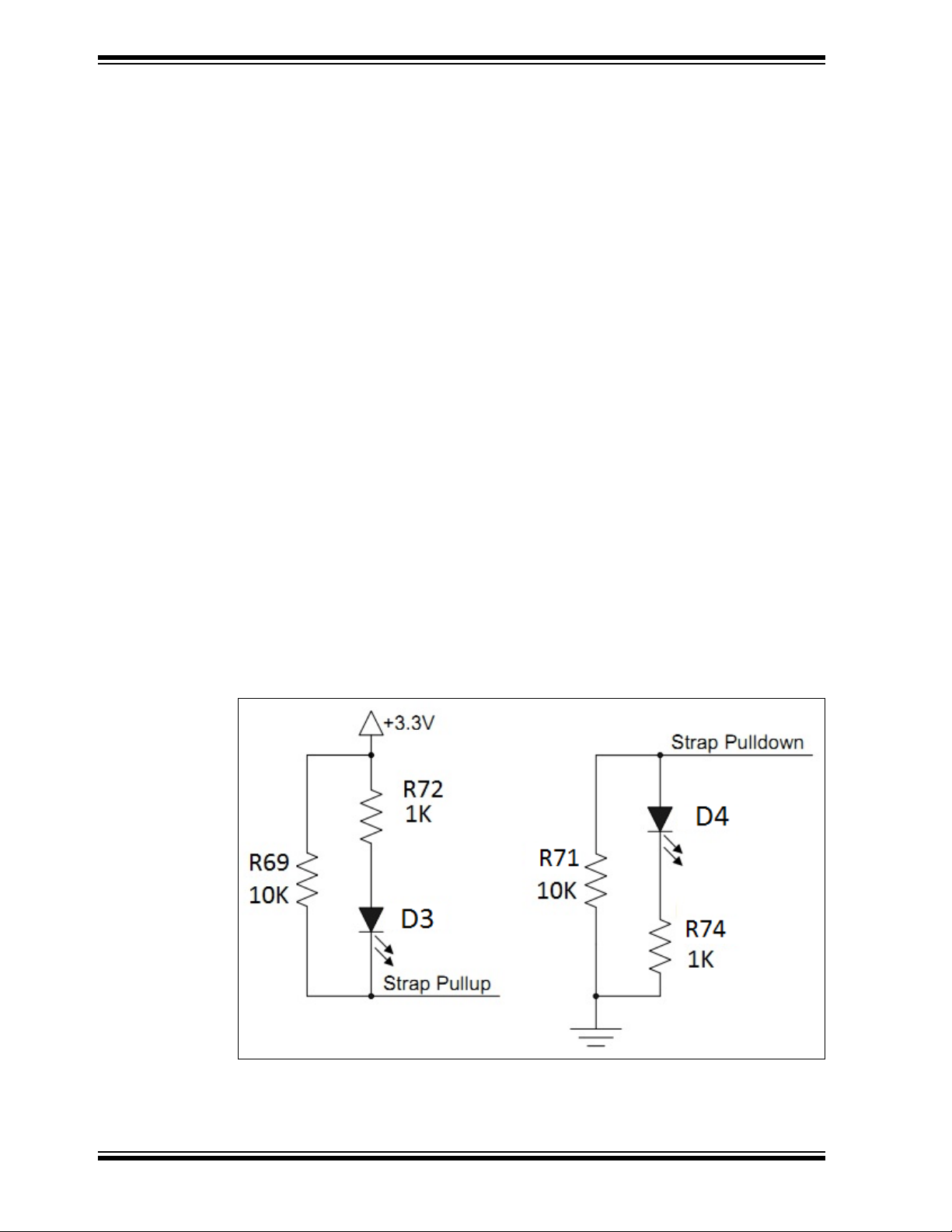
to a “1”, and another way to set the strap value to a “0”. Figure 4 illustrates the schematics connections with the D3 circuit as a pull-up, and the D4 circuit as a pull-down.
To illuminate D3, the LAN9252 will drive the cathode of the D3 low. To illuminate D4,
the LAN9252 will drive the cathode of the D4 high.
The J4 - J15 jumpers must be configured in pairs to identical settings in order to realize
the D3 circuit or the D4 circuit. The pairings are as follows:
-J4 & J7
-J6 & J9
-J5 & J8
- J15& J16
The following subsections detail the jumper pair settings, their associated strap settings, and the functional effects of setting the straps. All strap values are read during
power-up and on the rising edge of nRST signal. Once the strap value is set, the
LAN9252 will drive the LED’s high or low for illumination according the strap value. For
other designs which may use these pins as GPIOs refer to LAN9252 datasheet for
additional information. In those cases, internal default straps must be changed by an
2
I
C or SMI master or through EEPROM fields.
FIGURE 3-3: LED STRAP CIRCUIT
DS50002403A-page 16 2015 Microchip Technology Inc.
Page 17

Board Configuration
3.2.1.2 EEPROM CONFIGURATION
EEPROM_size_strap (J6 & J9): This strap determines the EEPROM size range.
A low selects 1K bits (128 x 8) through 16K bits (2K x 8)_24C16.
A high selects 32K bits (4K x 8) through 512K bits (64K x 8) or 4Mbits (512K x
8)_24C512.
TABLE 3-2: EEPROM SIZE CONFIGURATION
Header Pin Settings eeprom_size_strap Value Description
J6 & J9 1-2 (Default) 1 EEPROM size = 32K bits (4K x
8) through 4Mbits (512K x 8).
J6 & J9 2-3 0 EEPROM size = 1K bits (128 x
8) through 16K bits (2K x 8).
3.2.1.3 TX SHIFT STRAP
EtherCAT MII Port TX Timing Shift Strap is used to configure default value of EtherCAT
MII Port TX Timing Shift Strap “TX_SHIFT[1:0]”. These straps determine the value of
the MII TX Timing Shift for the MII.
TABLE 3-3: ETHERCAT MII PORT TX TIMING SHIFT STRAP OPTIONS
TX_SHIFT 1 TX_SHIFT 0 TX Timing Shift (ns)
0020
0 1 30 (Default)
100
1110
TABLE 3-4: MII TX TIMING SHIFT CONFIGURATIONS
Switch Short Pins TX_SHIFT[1:0] Switch KNOB Position
SW9 1-2 01 DOWN
SW10 1-3 UP
Note: For switch P/N: 450301014042, pin 1 is at the middle of the switch. To short
1-2, knob position must be in the 1-3 position, and vice versa.
3.2.1.4 COPPER AND FIBER STRAPS
The LAN9252 supports 100BASE-TX (Copper) and 100BASE-FX (Fiber) modes. In
100BASE-FX operation, the presence of the receive signal is indicated by the external
transceiver as either an open-drain, CMOS level, Loss of Signal (SFP) or a LVPECL
Signal Detect (SFF).
This EVB supports 100BASE-TX (Copper) and SFP 100BASE-FX (Fiber) modes. By
default Copper Mode is active. Fiber Mode is supported as an assembly option. To
select the Copper or Fiber Mode, the respective strap and signal routing resister
assembly options must to be configured.
Note: Vendor part number for SFP: Finisar/FTLF1217P2
2015 Microchip Technology Inc. DS50002403A-page 17
Page 18

EVB-LAN9252-3PORT EtherCAT® ESC PHY Connection Mode User’s Guide
3.2.1.4.1 Copper Mode Strap
The EVB-LAN9252-3PORT is set to Copper Mode by default. Tab le 3- 5 details the
required strap resistor settings for Copper Mode operation.
TABLE 3-5: COPPER MODE STRAP RESISTORS
Resistors Signal Names Description
R79 (10K) FXLOSEN Copper twisted pair for ports A and B further
determined by FXSDENA and FXSDENB
R76, R80 (10K) FXSDA/FXSDB Configures Port 0 and Port 1 to Copper
Mode
Note: R75, R77, and R78 must not be populated (DNP).
Additionally, the signal routing resistors detailed in Ta bl e 3- 6 must be assembled for
Copper mode operation.
TABLE 3-6: COPPER MODE SIGNAL ROUTING RESISTORS
Resistors Description
R17, R19,R21, R23 Port 0 Copper mode is Enabled
R31, R33, R35, R37 Port 1 Copper mode is Enabled
Note: R16, R18, R20, R22, R30, R32, R34, and R36 (0402 package) must not be
populated (DNP).
3.2.1.4.2 Fiber Mode Strap
The EVB-LAN9252 supports SFP type 100BASE-FX mode. To enable Fiber Mode, the
respective strap and signal routing resisters must be configured.
Note: Copper Mode related resistors must be DNP while Fiber Mode is active
(See Section 3.2.1.4.1 “Copper Mode Strap”).
Ta bl e 3- 7 details the required strap resistor settings for Fiber Mode operation.
TABLE 3-7: FIBER MODE STRAP RESISTORS
Resistors Description
R77 (10K) Configures Port 0 & 1 to FX_LOS Mode
R75, R78 (10K) Configures Port 0 & 1 to Fiber mode, respectively
Note: R76, R79, and R80 must not be populated (DNP).
Additionally, the signal routing resistors detailed in Ta bl e 3- 8 must be assembled for
Fiber Mode operation.
TABLE 3-8: FIBER MODE SIGNAL ROUTING RESISTORS
Resistors Description
R16, R18, R20, R22 Port 0 Fiber mode Enabled
R30, R32, R34, R36 Port 1 Fiber mode Enabled
Note: R17, R19, R21, R23, R31, R33, R35, and R37 (0402 package) must not be
populated (DNP).
DS50002403A-page 18 2015 Microchip Technology Inc.
Page 19

Board Configuration
3.2.1.4.3 FX-LOS Fiber Mode Strap
The EVB-LAN9252-3PORT is set to Copper Mode by default. Tab le 3- 9 details the
required strap resistor settings for FX-LOS Fiber Mode operation.
TABLE 3-9: FX-LOS FIBER MODE STRAP RESISTOR SETTINGS
R77 (10K) R79 (10K)
Populate DNP 3.3 A level above 2V selects FX-LOS for Port 0 and
Populate Populate 1.5 A level greater than 1.5V and below 2V selects
DNP Populate 0 (DEFAULT) A level of 0V selects FX-SD / copper twisted pair
Note: The above strap details describe the LAN9252 function. This EVB does not
support SFF Fiber Mode. Therefore, FX-SD related straps are not applicable.
3.2.2 LED Indicators
Reference
Voltage (V)
Function
Port1
FX-LOS for Port 0 and FX-SD / copper twisted
pair for Port 1, further determined by FXSDB
for Ports 0 and 1, further determined by FXSDA
and FXSDB
The D3, D4 and D7 LEDs are used to indicate the Link/Activity status on the corresponding EVB ports, as detailed in Tab le 3 -1 0. The Link/Act LED should be ON at each
port when the cable is present. If the Link/Act LED is not ON, it indicates there is an
issue with the connection or cable.
TABLE 3-10: D3, D4 AND D7 LINK/ACTIVITY LED STATUS INDICATORS
State Description
Off Link is down
Flashing Green Link is up, with activity
Steady Green Link is up, no activity
Additionally, the D5 LED is used as a RUN indicator (green) to show the AL status of
the EtherCAT State Machine (ESM), as detailed in Ta bl e 3 -11 .
TABLE 3-11: ESM AL STATUS
State Description
Off The device is in INITIALIZATON state
Blinking (on 200ms, off 200ms) The device is in PRE-OPERATIONAL state
Single Flash (on 200ms, off 1000ms) The device is in SAFE-OPERATIONAL state
On The device is in OPERATIONAL state
Flickering (on 50ms, off 50ms) The device is booting and has not yet entered the INI-
TIALIZATION state, or the device is in the BOOTSTRAP state and firmware download is in progress.
(Optional. Off when not implemented.)
Additionally, LED D10 is used as Error LED and the LED D9 is DNP.
3.2.3 EEPROM Switch
The EVB-LAN9252-3PORT utilizes 0x50 (7-bit) I2C slave addressing. The SW3 switch
can be used to select the A0, A1, and A2 address bits, as shown in Figure 3-4 and
Ta bl e 3 -1 2. The eighth bit of the slave address determines if the master device wants
to read or write to the EEPROM (24FC512).
2015 Microchip Technology Inc. DS50002403A-page 19
Page 20

EVB-LAN9252-3PORT EtherCAT® ESC PHY Connection Mode User’s Guide
FIGURE 3-4: SLAVE ADDRESS ALLOCATION
TABLE 3-12: EEPROM SWITCH
Ref. Des Description Settings
2
SW3 I
C EEPROM Address selection
(A0,A1,A2) see
Figure 3-4
3.2.4 SPI + 3 Port Mode Selection
3.2.4.1 SPI
ON for logic 0 (default)
OFF for logic 1
The SPI lines are directly connected to the SOC. No jumper settings are required for
SPI.
3.2.4.2 SPI/SQI/I
2
C AARDVARK
®
J11 & J12 connectors are used for Aardvark/SPI headers. Respective pin details are
given below in Table 3-13. Resisters R61, R62 & R122 are need to be populated to use
this option. By default, R61, R62 & R122 are DNP.
TABLE 3-13: SPI/SQI/I2C AARDVARK® PIN DETAILS
Signal Pin No
SCL J11.1
SDA J11.3
SCK J11.7
SCS# J11.9
SI(SIO0) J11.8
SO(SIO1) J11.5
SIO2 J12.3
SIO3 J12.4
3.2.4.3 3 PORT MODE
The following Assembly/jumper settings are used to configure LAN9252 in to 3-Port
mode.
3.2.4.3.1 Assembly of the Boards
The MII Female Connector (J27) is used to connect External PHY Board.
EVB-LAN8740 MII PHY Board have been used as External PHY Board as shown in
Figure 3-2.
DS50002403A-page 20 2015 Microchip Technology Inc.
Page 21

Board Configuration
3.2.4.3.2 External PHY - Power
The Jumper (J26) is used to supply “on-board 5V or delayed 5V” to external PHY
Board.
TABLE 3-14: EXTERNAL PHY BOARD PIN SETTINGS
Header Pin Settings Description
J26 1-2 Connects on-board 5V to an external PHY Board (Default)
J26 2-3 Connects Delayed 5V to an external PHY Board in Enhanced
Link detection
3.2.4.3.3 External PHY - MII Link
Connect MII Link from an external PHY board (EVB-LAN8740) to the 1st pin of J24
through jumpers as shown in Figure 3-2.
3.2.4.3.4 External PHY - MII Reset
Connect reset from an external PHY board (EVB-LAN8740) to the 3rd pin of J24
through jumpers as shown in Figure 3-2.
3.2.4.3.5 External PHY - CLK
The MII_CLK25 from LAN9252 is available on J24-12th pin and this signal has to be
routed to Master Clock of the External PHY.
Note: The EVB-LAN8740 is used for an External PHY. Refer to link
http://ww1.microchip.com/downloads/en/DeviceDoc/evb8740_user.pdf for
more details on EVB-LAN8740.
Remove on board crystal and connect MII-CLK25 from MII connector to the LAN8740
OSCO pin as shown below in Figure 3-5 (through Green wire).
FIGURE 3-5: LAN8740
2015 Microchip Technology Inc. DS50002403A-page 21
Page 22

EVB-LAN9252-3PORT EtherCAT® ESC PHY Connection Mode User’s Guide
3.2.4.3.6 Chip Mode Selection
Chip Mode Straps (J4,J7 &J5,J8) are used configure default value of EtherCAT Chip
Mode Strap “chip_mode_strap[1:0]”. This strap determines the number of active ports
and port types.
TABLE 3-15: CHIP MODE CONFIGURATION
Header
J4,J7 1-2 01 3 port downstream mode. Ports 1 and 2 are
J5,J8 2-3
Note: Default setting LAN9252 EVB — Chip mode 10 (3port downstream mode).
3.2.5 SoC
The EVB-LAN9252 supports both an on-board SoC and add-on SoC. By default, the
on-board SoC is enabled. However, an external add-on SoC can be connected via the
add-on SoC headers P8 and P9. The SoC selection is configured via the SW5 switch,
as detailed in the following subsections.
Pin
Settings
chip_mode_strap[1:0] Description
connected to internal PHYs A and B. Port 0
is connected to the external MII pins
Chip mode 00 and 11 are not supported by this EVB.
3.2.5.1 SOC SELECTION
Whenever the ADD ON PCB is used for SoC, then the Switch knob position must be
UP.
The SW5 switch selects the enabled SoC. The SW5 switch knob position must be down
(Text = “PIC”) to select the on-board PIC. If the switch knob position is up (Text = “PIM”),
then the add-on board/SoC is selected and the on-board PIC is always in the reset
state. Whenever an add-on board/SoC is used, the switch knob must be in the up position.
TABLE 3-16: SOC SWITCH CONFIGURATION
Switch Position Settings
SW5 DOWN PIC enabled
SW5 UP ADD ON BOARD enabled
3.2.5.2 ON-BOARD PIC
By default, the on-board Microchip PIC32MX795F512L (U7) is used as the default
SoC. The LAN9252 can be connected to the PIC using SPI interface. No jumper settings are required to establish SPI communications between PIC and LAN9252.
3.2.5.3 RESET
SW5 is used to reset the on-board PIC. The LAN9252 can also reset the SoC if the
reset pin is configured to output mode. For stability, a delay of approximately 180ms is
added from the 3.3V o/p to reset release.
3.2.5.4 ICSP HEADER
The programing is done using the ICSP header – J13. Table 3-17 shows the PIN details
of J13.
TABLE 3-17: J13 PIN DETAILS
J13 PIN No Signals Detail
1MLCR
DS50002403A-page 22 2015 Microchip Technology Inc.
Page 23

Board Configuration
TABLE 3-17: J13 PIN DETAILS (CONTINUED)
J13 PIN No Signals Detail
23V3
3GND
4PGD2
5PGC2
6NC
3.2.5.5 SOC EEPROM
The EVB-LAN9252 provides an optional SoC EEPROM. Some SoCs may require an
EEPROM. However, the PIC on-board SoC and PIC based add-on SoC boards do not
require this EEPROM.
3.2.5.6 ADD-ON SOC
An add-on board can be attached to the EVB-LAN9252 to use an add-on SoC. The
add-on board must be mounted to the P8 and P9 connectors (2x23, 100mil normal gold
plated berg stick). The SW5 switch must be in the up position when using an add-on
SoC. Additionally, the J10 2-pin jumper must be shorted to route power to the add-on
board from the EVB-LAN9252.
An ADD on BOARD can be used for SoC. At the connectors P8 & P9 (2X23, 100mil
normal gold platted berg stick) the ADD on BOARD need to be mounted. SW5 – switch
NOB position must be UP to use this option. Also J10 – 2 pin jumper must be short to
get the power for the ADD on BOARD.
3.2.5.7 ESC ID SELECT
The signals shown in Ta bl e 3 -1 8 are provided as EtherCAT ID selection for complex
ESCs. Switches SW7, SW8 and respective pull-up resistors are used to configure the
ID select signals high or low. By default, the EtherCAT
ID values is set to 5. To achieve
this, ID0 and ID2 are high via pull-up resistors, while the remainder of the ID select signals are low (ID1, ID3-ID15). When required, setting the respective switch knob to the
on position will change the ID select signal to low.
TABLE 3-18: ID SELECT SIGNALS
ID Selection Signal PIC PIN No SW PIN No Res Ref. Des
ID_SELECT_RB0 25 SW7.1 R123
ID_SELECT_RB1 24 SW7.2 R124
ID_SELECT_RB2 23 SW7.3 R126
ID_SELECT_RB3 22 SW7.4 R125
ID_SELECT_RB4 21 SW7.5 R127
ID_SELECT_RB5 20 SW7.6 R128
ID_SELECT_RB8 32 SW7.7 R129
ID_SELECT_RB9 33 SW7.8 R130
ID_SELECT_RB10 34 SW8.1 R131
ID_SELECT_RB11 35 SW8.2 R133
ID_SELECT_RB12 41 SW8.3 R134
ID_SELECT_RB13 42 SW8.4 R132
ID_SELECT_RC1 6 SW8.5 R135
ID_SELECT_RC2 7 SW8.6 R136
ID_SELECT_RC3 8 SW8.7 R137
ID_SELECT_RC4 9 SW8.8 R138
2015 Microchip Technology Inc. DS50002403A-page 23
Page 24

EVB-LAN9252-3PORT EtherCAT® ESC PHY Connection Mode User’s Guide
3.3 MECHANICALS
Figure 3-6 details EVB-LAN9252(SPI + 3 Port) mechanical dimensions. Dimensions
are in mm.
FIGURE 3-6: EVB-LAN9252 MECHANICAL DIMENSIONS
DS50002403A-page 24 2015 Microchip Technology Inc.
Page 25

EVB-LAN9252-3PORT
ETHERCAT® ESC PHY CONNECTION
MODE USER’S GUIDE
Appendix A. EVB-LAN9252-3PORT Evaluation Board
A.1 INTRODUCTION
This appendix shows the EVB-LAN9252-3PORT Evaluation Board.
FIGURE A-1: EVB-LAN9252-3PORT EVALUATION BOARD
2015 Microchip Technology Inc. DS50002403A-page 25
Page 26

EVB-LAN9252-3PORT EtherCAT® ESC PHY Connection Mode User’s Guide
NOTES:
DS50002403A-page 26 2015 Microchip Technology Inc.
Page 27

EVB-LAN9252-3PORT
ETHERCAT® ESC PHY CONNECTION
MODE USER’S GUIDE
Appendix B. EVB-LAN9252-3PORT Evaluation Board
Schematics
B.1 INTRODUCTION
This appendix shows the EVB-LAN9252-3PORT Evaluation Board Schematics.
2015 Microchip Technology Inc. DS50002403A-page 27
Page 28

DS50002403A-page 28 2015 Microchip Technology Inc.
BLOCK DIAGRAM :-"/ EVB
FIGURE B-1: BLOCK DIAGRAM
EVB-LAN9252-3PORT EtherCAT
®
ESC PHY Connection Mode User’s Guide
Page 29

2015 Microchip Technology Inc. DS50002403A-page 29
Reset Generator
POWER SUPPLY
(Rb)(Ra)
O
KR-T/3-W12-C
3 V REGULATOR, 3A
( 3V3 fixed when Rb=503e)
"3V3 Present"
Note:
1.POR -> Reset to ASIC & SOC (Defaul t)
2.RESET O/P from ASIC -> Reset to EX-PHY ( PORT2) & SOC :Only Ethercat sku
3.RESET from SOC (GPIO/RST-O/P) -> Reset to ASIC
4.RESET from Push Botton -> Rese t to ASIC & SOC
"Reset"
RESET Options
5V_SW
EN12_1
5V_EXT
3V3
3V3
5V
3V3
3V3
3V3
3V3
RST#
U2
TPS3125
SOT23_5
Threshold = 2.64V
Delay = 180ms
U2
TPS3125
SOT23_5
Threshold = 2.64V
Delay = 180ms
RESET#
1
GND
2
RESET
3
MR#
4
VDD
5
TP2
ORANGE
TP2
ORANGE
D2
Br_Red-RA
D2
Br_Red-RA
1
A2C
Q1
NDS355AN_NMOS
Q1
NDS355AN_NMOS
1
G
3
S
2
D
C5
0.1uFC50.1uF
R5
4.75K
1%
R5
4.75K
1%
U1
3_AmpU13_Amp
GND
3
VIN
2
ENABLE1TRIM
5
VOUT
4
J1J1
1
2
3
D1
GRND1GRN
1
A
2
C
TP9
BLACK
TP9
BLACK
R10R1
0
TP8
BLACK
TP8
BLACK
C6
0.1uFC60.1uF
FB1
2A/0.05DCR
FB1
2A/0.05DCR
R4A
33E
1%
R4A
33E
1%
C2
10uF
25V
C2
10uF
25V
C1
4.7uF
DNP
C1
4.7uF
DNP
R3
3.30K
1%
R3
3.30K
1%
TP1
RED
TP1
RED
R6
10.0K
1/10W
1%
R6
10.0K
1/10W
1%
12
C4
10uFC410uF
SW2
sw_pb_2P
SW2
sw_pb_2P
R7
100
1/10W
1%
R7
100
1/10W
1%
1 2
R8 1KR8 1K
C3
0.1uFC30.1uF
R9
2.2KR92.2K
U3
74LVC1G14
U3
74LVC1G14
2 4
53
1
R21KR2
1K
SW1
P/N:1101M2S3CQE2
Switch, SPDT, Slide
SW1
P/N:1101M2S3CQE2
Switch, SPDT, Slide
2
3
1
R4
470E
1%
R4
470E
1%
FIGURE B-2: POWER SUPPLY & RST
Schematics
Page 30

DS50002403A-page 30 2015 Microchip Technology Inc.
Note:
OSCVSS need to connect to Chip gnd.
Power Supply Filtering
Low ESR
(*short 1&2)
REG_EN
RBIAS
VDD12TX1
VDD12TX2
VDD12TX2
VDD12TX1
OSCO
OSCI
3V3
VDD33TXRX1
VDD33TXRX2
VDDCR
VDD33TXRX1
VDD33TXRX2
3V3
3V3
3V3 3V3
3V3
VDDCR
3V33V3
FXSDA/FXLOSA
IRQ
ATEST/FXLOSEN
RXPA
RXNA
TXNA
TXPA
TXNB
TXPB
RXNB
RXPB
FXSDB/FXLOSB
GPIO0
GPIO1
GPIO2
I2C2_SCL
I2C2_SDA
RST#
OSCI_Combined
C15
0.1uF
C15
0.1uF
C26 18pFC26 18pF
J14
HEADER 3X2
J14
HEADER 3X2
2
4
6
1
3
5
C12
1.0uF DNP
C12
1.0uF DNP
FB3 2A/0.05DCRFB3 2A/0.05DCR
C25
0.1uF
C25
0.1uF
C13
0.1uF
C13
0.1uF
C10
0.1uF
C10
0.1uF
C210.1uF C210.1uF
C180.1uF C180.1uF
C23
1.0uF
DNP
C23
1.0uF
DNP
C11
0.1uF
C11
0.1uF
C27 18pFC27 18pF
FB4 2A/0.05DCR
BLM18EG221SN1D
FB4 2A/0.05DCR
BLM18EG221SN1D
POWER
INT PORT0INT PORT1
OSC
I2C
OTHER
SIGNALS
GPIO
(Only for
Lan9252)
U4A
LAN9252
POWER
INT PORT0INT PORT1
OSC
I2C
OTHER
SIGNALS
GPIO
(Only for
Lan9252)
U4A
LAN9252
FXSDENA/FXSDA/FXLOSA
9
FXSDENB/FXSDB/FXLOSB
10
VDD33TXRX1
51
TXNA
52
TXPA
53
RXNA
54
RXPA
55
VDD12TX1
56
RBIAS
57
VDD33BIAS
58
VDD12TX2
59
RXPB
60
RXNB
61
TXPB
62
TXNB
63
VDD33TXRX2
64
OSCI
1
OSCO
2
OSCVDD12
3
OSCVSS
4
REG_EN
7
ATEST/FXLOSEN
8
RST#
11
IRQ
44
TESTMODE
41
I2CSCL/EESCL/TCK
43
I2CSDA/EESDA/TMS
42
LINKACTLED0/TDO/LEDPOL0/CHIP_MODE0
48
LINKACTLED1/TDI/LEDPOL1/CHIP_MODE1
46
RUNLED/LEDPOL2/E2PSIZE
45
VDD33
5
VDDIO114VDDIO220VDDIO332VDDIO437VDDIO5
47
VDDCR16VDDCR224VDDCR3
38
GND
65
C220.1uF C220.1uF
C9
1.0uF
DNP
C9
1.0uF
DNP
R167
100K
DNP
R167
100K
DNP
C14
0.1uF
C14
0.1uF
C24
0.1uF
C24
0.1uF
R166
100K
DNP
R166
100K
DNP
C16
0.1uF
C16
0.1uF
C20470pF C20470pF
OSCILLATOR
Y425MHz
DNP
OSCILLATOR
Y425MHz
DNP
OE
1
VCC4GND
2
OUT
3
FB2 2A/0.05DCRFB2 2A/0.05DCR
R10 12.1K
1%
R10 12.1K
1%
C85
0.1uF
DNP
C85
0.1uF
DNP
Y1
25.000MHz
25ppm
Y1
25.000MHz
25ppm
1 2
C7
1.0uF
DNP
C7
1.0uF
DNP
FB5
2A/0.05DCR
FB5
2A/0.05DCR
C17
0.1uF
C17
0.1uF
C19
1uF
C19
1uF
C8
0.1uFC80.1uF
FIGURE B-3: LAN9252
EVB-LAN9252-3PORT EtherCAT
®
ESC PHY Connection Mode User’s Guide
Page 31

2015 Microchip Technology Inc. DS50002403A-page 31
Note:
Capacitors C10 through C13 are optional for EMI purposes
and are not populated on the LAN8740/41 evaluation board.
These capacitors are required for operation in an EMI
constrained environment.
LED1 (Green) = LINK/ACT
LED2 (Yellow) = SPEED
Note:
Capacitors C10 through C13 are optional for EMI purposes
and are not populated on the LAN8740/41 evaluation board.
These capacitors are required for operation in an EMI
constrained environment.
LED1 (Green) = LINK/ACT
LED2 (Yellow) = SPEED
COP-RXPA
COP-TXNA
COP-RXNA
COP-TXPA
COP-RXPB
COP-TXNB
COP-RXNB
COP-TXPB
VDD33TXRX2
VDD33TXRX1
FX_SFP-RXPA
FX_SFP-RXNA
TXPA
TXNA FX_SFP-TXNA
FX_SFP-TXPA
RXPA
RXNA
FX_SFP-RXPB
FX_SFP-RXNB
TXPB
TXNB FX_SFP-TXNB
FX_SFP-TXPB
RXPB
RXNB
R17 0R17 0
R35 0R35 0
R22 0
DNP
R22 0
DNP
R33 0R33 0
XMIT
RCV
75
75 75
1000 pF 2 kV
RJ45
1
4 & 5
2
3
7 & 8
6
75
GRN
YEL
T1
Pulse J0011D01BNL
XMIT
RCV
75
75 75
1000 pF 2 kV
RJ45
1
4 & 5
2
3
7 & 8
6
75
GRN
YEL
T1
Pulse J0011D01BNL
RD+
3
RXCT
5
RD-
6
TD+
1
TXCT
4
TD-
2
CHS GND
8
GND13GND114MTG15MTG1
16
NC
7
C
10
A
9
C1
11
A1
12
XMIT
RCV
75
75 75
1000 pF 2 kV
RJ45
1
4 & 5
2
3
7 & 8
6
75
GRN
YEL
T2
Pulse J0011D01BNL
XMIT
RCV
75
75 75
1000 pF 2 kV
RJ45
1
4 & 5
2
3
7 & 8
6
75
GRN
YEL
T2
Pulse J0011D01BNL
RD+
3
RXCT
5
RD-
6
TD+
1
TXCT
4
TD-
2
CHS GND
8
GND13GND114MTG15MTG1
16
NC
7
C
10
A
9
C1
11
A1
12
C29
10pF
50V
5%
DNP
C29
10pF
50V
5%
DNP
R23 0R23 0
C36
10pF
50V
5%
DNP
C36
10pF
50V
5%
DNP
C31
10pF
50V
5%
DNP
C31
10pF
50V
5%
DNP
R30 0
DNP
R30 0
DNP
R27
49.9
1/10W
1%
R27
49.9
1/10W
1%
R38 0
RES1210
R38 0
RES1210
R20 0
DNP
R20 0
DNP
R31 0R31 0
R13
49.9
1/10W
1%
R13
49.9
1/10W
1%
R25
49.9
1/10W
1%
R25
49.9
1/10W
1%
R24 0
RES1210
R24 0
RES1210
C33
10pF
50V
5%
DNP
C33
10pF
50V
5%
DNP
R21 0R21 0
R11
49.9
1/10W
1%
R11
49.9
1/10W
1%
R36 0
DNP
R36 0
DNP
R28
49.9
1/10W
1%
R28
49.9
1/10W
1%
C28
10pF
50V
5%
DNP
C28
10pF
50V
5%
DNP
C35
10pF
50V
5%
DNP
C35
10pF
50V
5%
DNP
R14
49.9
1/10W
1%
R14
49.9
1/10W
1%
R290R29
0
C32
0.022uF
50V
10%
C32
0.022uF
50V
10%
R37 0R37 0
C37
0.022uF
50V
10%
C37
0.022uF
50V
10%
R150R15
0
R18 0
DNP
R18 0
DNP
R16 0
DNP
R16 0
DNP
C30
10pF
50V
5%
DNP
C30
10pF
50V
5%
DNP
R26
49.9
1/10W
1%
R26
49.9
1/10W
1%
R12
49.9
1/10W
1%
R12
49.9
1/10W
1%
R34 0
DNP
R34 0
DNP
C34
10pF
50V
5%
DNP
C34
10pF
50V
5%
DNP
R19 0R19 0
R32 0
DNP
R32 0
DNP
FIGURE B-4: COPPER MODE INTERFACE
Schematics
Page 32

DS50002403A-page 32 2015 Microchip Technology Inc.
Fiber Port 0 :SFP Interface
Fiber Port 1 :SFP Interface
Note:Place
capacitors,
and resistors
close to FOT
Note:Place
resistors
close to
ASIC
Note:Place
capacitors,
and resistors
close to FOT
Note:Place
resistors
close to
ASIC
SFP_VCCT
SFP_VCCR
SFP_TD-
SFP_TD+
SFP_RD-
SFP_RD+
SFP_VCCT2
SFP_VCCR2
SFP_TD2-
SFP_TD2+
SFP_RD2-
SFP_RD2+
SFP_VCCT
SFP_VCCT2
3V3
3V3
3V3
3V3
FXSDA/FXLOSA
FXSDB/FXLOSB
FX_SFP-TXPA
FX_SFP-RXNA
FX_SFP-RXPA
FX_SFP-TXNA
FX_SFP-RXNB
FX_SFP-RXPB
FX_SFP-TXPB
FX_SFP-TXNB
+
C50
10uF
16V
DNP
+
C50
10uF
16V
DNP
C47
0.1uF
C47
0.1uF
R49
130
R49
130
C42
0.1uF
C42
0.1uF
+
C48
10uF
16V
+
C48
10uF
16V
R56
4.7K
R56
4.7K
C39 0.1uFC39 0.1uF
C38 0.1uFC38 0.1uF
R50
130
R50
130
L3 1uHL3 1uH
C44
0.1uF
C44
0.1uF
C41 0.1uFC41 0.1uF
R57
4.7K
R57
4.7K
C49
0.1uF
C49
0.1uF
+
C56
10uF
16V
+
C56
10uF
16V
R58
4.7K
R58
4.7K
C43 0.1uFC43 0.1uF
C40 0.1uFC40 0.1uF
R48
100
R48
100
L1 1uHL1 1uH
R45
49.9
R45
49.9
R59
4.7K
R59
4.7K
R41
49.9
R41
49.9
C45 0.1uFC45 0.1uF
R46
49.9
R46
49.9
C57
0.1uF
C57
0.1uF
R42
49.9
R42
49.9
R53
4.7K
R53
4.7K
L4 1uHL4 1uH
R54
4.7K
R54
4.7K
+
C52
10uF
16V
+
C52
10uF
16V
R4482R44
82
R55
4.7K
R55
4.7K
R47
100
R47
100
+
C54
10uF
16V
+
C54
10uF
16V
J3
FTLF1217P2
J3
FTLF1217P2
VeeT1TXFault2TX Disable3MOD-DEF(2)4MOD-DEF (1)5MOD-DEF (0)6Rate Select7LOS8VeeR9VeeR1
10
VeeR311VeeR2
14
RD-
12
RD+
13
VccR
15
VccT
16
VeeT2
17
TD+
18
TD-
19
VeeT1
20
21
21
22
22
23
23
24
24
25
25
26
26
27
27
28
28
29
29
30
30
31
31
C51
0.1uF
C51
0.1uF
R4382R43
82
L2 1uHL2 1uH
R60
4.7K
R60
4.7K
J2
FTLF1217P2
J2
FTLF1217P2
VeeT1TXFault2TX Disable3MOD-DEF(2)4MOD-DEF (1)5MOD-DEF (0)6Rate Select7LOS8VeeR9VeeR1
10
VeeR311VeeR2
14
RD-
12
RD+
13
VccR
15
VccT
16
VeeT2
17
TD+
18
TD-
19
VeeT1
20
21
21
22
22
23
23
24
24
25
25
26
26
27
27
28
28
29
29
30
30
31
31
R51
130
R51
130
C53
0.1uF
C53
0.1uF
C55
0.1uF
C55
0.1uF
R4082R40
82
+
C46
10uF
16V
DNP
+
C46
10uF
16V
DNP
R52
130
R52
130
R3982R39
82
FIGURE B-5: SFP INTERFACE
EVB-LAN9252-3PORT EtherCAT
®
ESC PHY Connection Mode User’s Guide
Page 33

2015 Microchip Technology Inc. DS50002403A-page 33
GPIO [0:2] & LED_POL_Strap
LINK/ACT
RUNLED
LINK/ACT
GPIO0 =LED0,LEDPOL0,MNGT0
GPIO1 = LED1,LEDPOL1,MNGT1
GPIO2 = LED2,LEDPOL2,E2PSIZE
Note:
--To use GPIOs as LED
* Short 2-3 of both jumpers (ex. for GPIO0 short 2-3 of J4 & J7)
1 The LED is set as active low,
MNGT0
The LED is set as active high.
MNGT1
0
Signal Name Connector
J4,J7 (1&2)
LED Polarity StrapLogic
E2ESIZE
J4,J7 (2&3)
J5,J8 (1&2)
J5,J8 (2&3)
10J6,J9 (1&2)
J6,J9(2&3)
The LED is set as active low,
The LED is set as active high.
The LED is set as active low,
EEPROM Size=32K bits (4K x 8) through 512K bits (64K x 8) or 4Mbits (512K x 8) (LAN9252 only)
The LED is set as active high.
EEPROM Size=1K bits (128 x 8) through 16K bits (2K x 8)
1
0
Management/LED Polarity Strap
I2C EEPROM
TH IC.
Different sizes can be mounted
I2C EEPROM Lower size
Below 16K(2K X 8)
I2C EEPROM Higher size
Above 16K(2K X 8)
'HIDXOW
&RSSRUPRGH
5 '135 $VVHPEOH
6HOHFWV);6'FRSSHUWZLVWHGSDLUIRUSRUWV$DQG%IXUWKHUGHWHUPLQHG
E\);6'(1$DQG);6'(1%
5 .5 .
/HYHORI9VHOHFWV);/26IRUSRUW$DQG
);6'&RSSHUWZLVWHGSDLUIRUSRUW%IXUWKHUGHWHUPLQHGE\);6'(1%
5 $VVHPEOH5 '13
$ERYH9VHOHFWV);/26IRUSRUWV$DQG%
FX_Los_Strap_1 & 2 FX_Mode_Strap_1 & 2
'HIDXOW
&RSSRUPRGH
55$VVHPEOH
55 '13
)LEHU0RGH
55$VVHPEOH
55 '13
LINK/ACT LED2
TX_SHIFT1TX_SHIFT0 MII TX Timing Shift
000 ns
10 ns01
20 ns10
30 ns11
MII TX Shift Timing
LED1_CATHODE
GPIO1
GPIO1
LED1_ANODE
LED2_ANODE
LED0_CATHODE
LED2_CATHODE
GPIO0
GPIO0 GPIO2
GPIO2
LED0_ANODE
LED0_ANODE
LED0_CATHODE
LED1_ANODE
LED1_CATHODE
LED2_ANODE
LED2_CATHODE
I2C2_2
I2C2_3
I2C2_7
I2C2_1
LEDPOL6_ANODE
LEDPOL6_CATHODE
MII_LINKPOL
LEDPOL6_ANODE
LEDPOL6_CATHODE
LEDPOL6_ANODE
LED0_CATHODE
3V33V3 3V3
3V3
3V3
3V3
3V3
3V3
3V3
3V3
3V3 3V3
GPIO0
GPIO1
GPIO2
I2C2_SDA
I2C2_SCL
ATEST/FXLOSEN
FXSDA/FXLOSA
FXSDB/FXLOSB
MII_LINKPOL
TX_SHIFT0 TX_SHIFT1
D9
LED
DNP
D9
LED
DNP
1
A2C
SW9
JS102011CQN
SW9
JS102011CQN
1
2
3
C58
0.1uF
C58
0.1uF
R77
10K
DNP
R77
10K
DNP
R76 10KR76 10K
J9J9
123
SW3
SW DIP-4/SM
SW3
SW DIP-4/SM
1
2
3
4
8
7
6
5
R141 10KR141 10K
R80 10KR80 10KR79
10K
R79
10K
J8J8
123
D5
GRND5GRN
1
A2C
R75 10KDNPR75 10KDNP
R654.7K R654.7K
J4J4
123
J6J6
123
R664.7K R664.7K
J5J5
123
R78 10KDNPR78 10KDNP
J16J16
123
R71
10.0K
R71
10.0K
12
SW10
JS102011CQN
SW10
JS102011CQN
1
2
3
R682KR68
2K
R731KR73
1K
R644.7K R644.7K
R672KR67
2K
J7J7
123
R69
10.0K
R69
10.0K
12
D4
GRND4GRN
1
A2C
R142 10KR142 10K
D3
GRND3GRN
1
A2C
R741KR74
1K
D7
LEDD7LED
1
A2C
J15J15
123
R634.7K R634.7K
U5
24FC04U524FC04
GND
4
VCC
8
SDA
5
SCL
6
A0
1
A1
2
A2
3
WP
7
R140
332
1/10W
1%
R140
332
1/10W
1%
12
R721KR72
1K
R139
10.0K
R139
10.0K
12
R70
10.0K
R70
10.0K
12
FIGURE B-6: STRAP, GPIO, I2C & FXLOS
Schematics
Page 34

DS50002403A-page 34 2015 Microchip Technology Inc.
Board to Board Connectors for SoC
Host SOC EEPROM
I2C EEPROM
Only for Host SOC
Short 1 -2 = To Reset ASIC from SoC-GPIO
Short 2-3 = To Reset SoC from ASIC
5V power to
HOST SOC board
from EVB Board
I2C1_SCL
I2C1_SDA
I2C3_2
I2C3_3
I2C3_7
I2C3_1
SYS_RESETN
VDD_5V
VDD3V3EXP
SPI_CE#
STORM_SIO3
I2C1_SDA
SPI_MISO
STORM_SIO2
I2C1_SCL
RST_GPIO
SPI_MOSI
SPI_CLK
RST_GPIO
SYS_RESETN
VDD_5V
VDD3V3EXP
3V33V3
5V
IRQ
PME_LATCH1
FIFOSEL_LATCH0
PME_LATCH1
FIFOSEL_LATCH0
IRQ
STORM_SIO3
SPI_CE#
SPI_MISO
STORM_SIO2
SPI_MOSI
SPI_CLK
RST#
I2C1_SCL
I2C1_SDA
SYS_RESETN
RST_GPIO
R862K R862K
C59
0.1uF
C59
0.1uF
J10J10
1 2
U6
24FC512U624FC512
GND
4
VCC
8
SDA
5
SCL
6
A0
1
A1
2
A2
3
WP
7
P8
HEADER 23x2
P8
HEADER 23x2
1
3
5
7
9
11
13
15
17
19
21
23
25
27
29
31
33
35
37
39
41
43
45
2
4
6
8
10
12
14
16
18
20
22
24
26
28
30
32
34
36
38
40
42
44
46
C60 0.1uF
DNP
C60 0.1uF
DNP
R824.7K R824.7K
R844.7K R844.7K
D6
DIODED6DIODE
1 2
R814.7K R814.7K
R854.7K R854.7K
SW11
JS102011CQN
SW11
JS102011CQN
1
2
3
TP10
ORANGE
TP10
ORANGE
P9
HEADER 23x2
P9
HEADER 23x2
1
3
5
7
9
11
13
15
17
19
21
23
25
27
29
31
33
35
37
39
41
43
45
2
4
6
8
10
12
14
16
18
20
22
24
26
28
30
32
34
36
38
40
42
44
46
SW4
SW DIP-4/SM
SW4
SW DIP-4/SM
1
2
3
4
8
7
6
5
R832K R832K
FIGURE B-7: B2B INTERFACE
EVB-LAN9252-3PORT EtherCAT
®
ESC PHY Connection Mode User’s Guide
Page 35

2015 Microchip Technology Inc. DS50002403A-page 35
Decap for U3
RESET
SW Position 1-2 & 4-5 = PIM ON
SW Position 2-3 & 5-6 = PIC ON
J73 - SPI AARDVAR HEADER
J73+J74 - SPI STROM HEAD ER
Aardvark / SPI Storm- Connector
MCLR
PIM_MCLR
PGD2
PGC2
PIM_MCLRPIC_MCLR
MCLR
PIC_MCLR
STORM_SIO2
STORM_SIO3
SPI_CE#
SPI_MOSI
SPI_MISO
SPI_CLK
ID_SELECT_RB5
ID_SELECT_RB4
ID_SELECT_RB3
ID_SELECT_RB2
ID_SELECT_RB1
ID_SELECT_RB0
ID_SELECT_RB8
ID_SELECT_RB9
ID_SELECT_RB10
ID_SELECT_RB11
ID_SELECT_RB12
ID_SELECT_RB13
ID_SELECT_RB0
ID_SELECT_RB1
ID_SELECT_RB2
ID_SELECT_RB8
ID_SELECT_RB3
ID_SELECT_RB4
ID_SELECT_RB5
ID_SELECT_RB9
ID_SELECT_RB10
ID_SELECT_RB11
ID_SELECT_RB12
ID_SELECT_RC3
ID_SELECT_RB13
ID_SELECT_RC1
ID_SELECT_RC2
ID_SELECT_RC4
ID_SELECT_RC1
ID_SELECT_RC3
ID_SELECT_RC4
ID_SELECT_RC2
3V3 3V3
3V3
3V3
3V3
3V3
SYS_RESETN
SPI_MOSI
SPI_MISO
SPI_CLK
SPI_CE#
I2C1_SDA
I2C1_SCL
IRQ
I2C2_SCL
I2C2_SDA
FIFOSEL_LATCH0
PME_LATCH1
STORM_SIO3
STORM_SIO2
RST_GPIO
SW8
SW DIP-8
SW8
SW DIP-8
1
2
3
4
5
6
7
8
16
15
14
13
12
11
10
9
R12610K R12610K
R13710K R13710K
R13110K R13110K
C64 11pFC64 11pF
R12710K R12710K
D10
GRN
No
D10
GRN
No
1
A2C
C61 0.1uFC61 0.1uF
C670.1uF C670.1uF
R13210K R13210K
R12810K R12810K
R61 0R61 0
R13310K R13310K
J11J11
2
4
6
8
10
1
3
5
7
9
R13010K R13010K
C680.1uF C680.1uF
R90 1K
No
R90 1K
No
J12J12
341
2
C690.1uF C690.1uF
R62 0R62 0
Y2
32KhzY232Khz
R13410K R13410K
C700.1uF C700.1uF
R12910K R12910K
C66 20pFC66 20pF
SW7
SW DIP-8
SW7
SW DIP-8
1
2
3
4
5
6
7
8
16
15
14
13
12
11
10
9
R13510K R13510K
PIM1
PIM CONN
PIM1
PIM CONN
1
2
3
4
5
6
7
8
9
10
11
12
13
14
15
16
17
18
19
20
21
22
23
24
25
26272829303132333435363738394041424344454647484950
9998979695949392919089888786858483828180797877
76
75
74
73
72
71
70
69
68
67
66
65
64
63
62
61
60
59
58
57
56
55
54
53
52
100
51
C710.1uF C710.1uF
R122 0R122 0
C65 20pFC65 20pF
U7
PIC32MX795F512L-80I/PT
U7
PIC32MX795F512L-80I/PT
AERXERR
1
VDD
2
PMD5
3
PMD6
4
PMD7
5
RC1
6
RC2
7
RC3
8
RC4
9
PMA5
10
PMA4
11
AERXDV
12
MCLR
13
AERXCLK/AEREFCLK
14
VSS
15
VDD1
16
TMS/RA0
17
AERXD0
18
AERXD1
19
AN5/C1IN+/VBUSON/CN7/R B5
20
RB4
21
RB3
22
RB2
23
RB1
24
RB0
25
PGEC2/AN6/RB626PGED2/AN7/RB727AERXD228AERXD329AVDD30AVSS31RB832RB933RB1034AETXERR35VSS136VDD237TCK/RA138SCK439SS440AECRS41MII2_COL42PMA1/AETXD3/PMALH43PMALL/PMA0/AETXD244VSS245VDD346AETXD047AETXD148SDI449SDO4
50
USBID/RF3
51
SDA3/SDI3/U1RX/RF2
52
SCL3/SDO3/U1TX/R F8
53
VBUS
54
VUSB
55
D-/RG3
56
D+/RG2
57
SCL2
58
SDA2
59
TDI/RA4
60
TDO/RA5
61
VDD4
62
OSC1/CLKI/RC12
63
OSC2/CLKO/RC15
64
VSS3
65
AETXCLK
66
AETXEN
67
EMDIO
68
SS1/IC2/RD9
69
PMCS2
70
EMDC
71
INT0
72
SOSCI/CN1/RC13
73
SOSCO/T1CK/CN0/RC14
74
VSS4
75
OC2/RD176OC3/RD277OC4/RD3
78
PMD1279PMD13
80
PMWR
81
PMRD
82
PMD1483PMD15
84
VCAP/VDDCORE
85
VDD5
86
PMD1187PMD10
88
PMD989PMD8
90
RA691RA7
92
PMD093PMD1
94
TRD2/RG14
95
RG1296RG13
97
PMD298PMD399PMD4
100
R12310K R12310K
C720.1uF C720.1uF
R89 1KR89 1K
C63 11pFC63 11pF
C750.1uF C750.1uF
R88
4.7K
R88
4.7K
R13610K R13610K
C730.1uF C730.1uF
R12410K R12410K
SW5
JS202011CQN
SW5
JS202011CQN
1
2
3
4
5
6
J13
DBG ICSP Header
J13
DBG ICSP Header
1
2
3
4
5
6
R87 OE
DNP
R87 OE
DNP
SW6
sw_pb_2P
SW6
sw_pb_2P
C740.1uF C740.1uF
Y3
8 MhzY38 Mhz
R12510K R12510K
R168 0R168 0
R13810K R13810K
C62 10uFC62 10uF
FIGURE B-8: PIM+ON-BOARD-PIC32MX
Schematics
Page 36

DS50002403A-page 36 2015 Microchip Technology Inc.
Ethercat Expansion Mode (4 Port Mode)
Supply selection for Combined and Separate
J70 = Open for 3 Port mode
(*short)
COMBINED MODESEPARATE MODEConnector Number
5V - J63 (1&2) Short Open
RST# - J64 (1&2) Short Open
Note:
Ethercat Expansion mode short J72- 1&2
Place to near MII conn,to connect fly wires.
MII_RXCLK
MII_MDC
MII_MDIO
MII_TXEN
MII_TXD 0
MII_TXD 1
MII_TXD 2
MII_TXD 3
MII_RXER
MII_RXD3
MII_RXD2
MII_RXD1
MII_RXDV
MII_RXD0
MII_CLK2 5
MII_TXD 2
MII_TXD 3
MII_RXER
MII_MDIO
MII_MDC
MII_LINK
MII_RXD3
MII_RXD1
MII_RXD2
MII_RXD0
MII_RXDV
MII_RXCLK
MII_CLK2 5
MII_TXD 0
MII_TXEN
MII_TXD 1
MII_TXD 2
MII_TXD 3
MII_TXD 0
MII_TXEN
MII_TXD 1
MII_TXD 2
MII_CLK2 5
MII_TXD 3
MII_RXD3
MII_RXD1
MII_RXD2
MII_RXD0
MII_RXDV
MII_RXCLK
Brd2_5V
Brd2_RST
Brd2_OSC
Brd2_RST
Brd2_5V
Brd2_5V
Brd2_RST
Brd2_RST
Brd2_OSC
Brd2_5V
3V3
5V
SPI_CE#
STORM_SIO3
STORM_SIO2
SPI_MISO
SPI_MOSI
FIFOSEL_LATCH0
PME_LATCH1
MII_LINKPOL
TX_SHIFT0
TX_SHIFT1
MII_RXD0
MII_RXD1
MII_RXD2
MII_RXD3
MII_RXDV
MII_RXCLK
MII_MDIO
MII_MDC
MII_TXD 0
MII_TXD 1
MII_TXD 2
MII_TXD 3
MII_TXEN
MII_CLK2 5
MII_RXER
RST#
OSCI_Combined
SPI_CLK
MII_LINK
J19J19
12
J18J18
1
2
3
4
5
6
7
8
9
10
11
12
13
14
15
16
17
18
19
20
21
22
R143
4.7K
R143
4.7K
U4B
LAN9252
U4B
LAN9252
SYNC/LATCH1
18
SYNC/LATCH0
34
A4/DIGIO12/GPI12/GPO12/MII_RXD0
27
A3/DIGIO11/GPI11/GPO11/MII_RXDV
26
A2/ALEHI/DIGIO10/GPI10/GPO10/LINKACTLED2/MII_LINKPOL/LEDPOL6
29
A1/ALELO/OE_EXT/MII_CLK25
25
A0/D15/AD15/DIGIO9/GPI9/GPO9/MII_RXER
33
D14/AD14/DIGIO8/GPI8/GPO8/MII_TXD3/TX_SHIFT1
15
D13/AD13/DIGIO7/GPI7/GPO7/MII_TXD2/TX_SHIFT0
16
D12/AD12/DIGIO6/GPI6/GPO6/MII_TXD1
21
D11/AD11/DIGIO5/GPI5/GPO5/MII_TXD0
22
D10/AD10/DIGIO4/GPI4/GPO4/MII_TXEN
23
D9/AD9/LATCH_IN/SCK
19
D8/AD 8/DIGIO2 /GPI2/GPO 2/MII_MDIO
40
D7/AD 7/DIGIO1 /GPI1/GPO 1/MII_MDC
39
D6/AD 6/DIGIO0 /GPI0/GPO 0/MII_RXC LK
36
D5/AD5/OUTVALID/SCS#
50
D3/AD3/WD_TRIG/SIO3
35
D2/AD2/SOF/SIO2
12
D1/AD1/EOF/SO/SIO1
13
D0/AD0/WD_ST ATE/SI/SIO0
17
RD/RD_WR/DIGIO15/GPI15/GPO15/MII_RXD3
31
WR/ENB/DIGIO14/GPI14/GPO14/MII_RXD2
30
CS/DIGIO13/GPI13/GPO13/MII_RXD1
28
D4/AD 4/DIGIO3 /GPI3/GPO 3/MII_LINK
49
J21J21
1 2
J20J20
1 2
R14410K DNPR14410K DNP
TP4TP4
J17J17
1
2
3
4
5
6
7
8
9
10
11
12
13
14
15
16
17
18
19
20
21
22
TP3TP3
J23J23
1 2
J22
(*open)
J22
(*open)
1 2
FIGURE B-9: EXPANSION MODE INTERFACE
EVB-LAN9252-3PORT EtherCAT
®
ESC PHY Connection Mode User’s Guide
Page 37

Standard Link Detection
PHY Power sequencing with transceiver power Down/Reset
Standard Link Detection
PHY reset release delay with transceiver power Down/Reset
DNP
Enhanced Link Detection
uC detects auto-negotiation restart command and
power down PHY and transceiver / resets PHY and transceiver
MII Female for External PH Y Board
Note:
Ethercat external board (Port2_TXER,COL,CRS signals not used)
External Port 2 Interface
Note:
Default open.
When used J79 DNP
200 mS
300 mS
500 mS
180mS=176.17nF
800mS=180.1nF
180mS=176.17nF
800mS=180.1nF
Link Detection selection
Standard
J79
Enhanced
Short 1&2
Short 2&3
(1-2*)
Link Detection Selection
5V
RST_Delay
MCLR
MCLR
ICSPDAT
ICSPCLK
ICSPDAT
ICSPCLK
MII_MDIO
RC2
MII_MDC
RC2
RC3
RC5
RC5
RA4
RC3
RC4
MII_MDIO
MII_RXD1
MII_TXD 3
MII_RXER
MII_RXD3
MII_TXEN
MII_MDC
MII_RXD0
MII_TXD 2
MII_TXD 1
CRS
COL
MII_RXDV
MII_RXD2
MII_TXD 0
MII_RXCLK
TXER
MII_CLK2 5
RST_Delay
5V_Delay
VCC_EXT0
5V_Delay
RC4
VCC_EXT0RA4
RC4
3V3
5V
5V
5V
3V33V3
5V
3V3
3V3
3V3
VCC_EXT0
RST#
RST#
RST#
MII_TXD 0
MII_TXD 1
MII_TXD 2
MII_TXD 3
MII_TXEN
MII_CLK2 5
MII_RXER
MII_RXD0
MII_RXD1
MII_RXD2
MII_RXD3
MII_RXDV
MII_RXCLK
MII_MDIO
MII_MDC
MII_LINK
R157
100K
R157
100K
R147
10.0K
R147
10.0K
C80
DNP
C80
DNP
U9
NCP308SNADJT1G
U9
NCP308SNADJT1G
RESET
1
GND
2
MR
3
CT
4
SENSE
5
VDD
6
R163
100K
R163
100K
R1481KR148
1K
C77 0.1uFC77 0.1uF
U8
NCP308SNADJT1G
U8
NCP308SNADJT1G
RESET
1
GND
2
MR
3
CT
4
SENSE
5
VDD
6
J29J29
12
R152
ZERO
R152
ZERO
C81
DNP
C81
DNP
J25J25
1
3 4
2
5 6
7 8
J27
5173277-2
J27
5173277-2
+5V4
40
GND1
39
GND2
38
GND3
37
GND4
36
GND5
35
GND6
34
GND7
33
GND8
32
GND9
31
GND10
30
GND11
29
GND12
28
GND13
27
GND14
26
GND15
25
GND16
24
GND17
23
GND18
22
+5V3
21
+5V1
1
MDIO
2
MDC
3
RXD3
4
RXD2
5
RXD1
6
RXD0
7
RX_DV
8
RX_CLK
9
RX_ER
10
TX_ER
11
TX_CLK
12
TX_EN
13
TXD0
14
TXD1
15
TXD2
16
TXD3
17
COL
18
CRS
19
+5V2
20
414142
42
C8210uF C8210uF
TP6
WHITE
TP6
WHITE
R156
100K
R156
100K
R161 33ER161 33E
R153
374E
R153
374E
J28
DBG ICSP Header
J28
DBG ICSP Header
1
2
3
4
5
6
C78
0.001uF
C78
0.001uF
J26J26
123
R1621KR162
1K
C83 0.1uFC83 0.1uF
R159 1KR159 1K
D8 IN4148D8 IN4148
12
R154
374E
R154
374E
R149
ZERO
R149
ZERO
R165
10.0K
DNP
R165
10.0K
DNP
TP5
WHITE
TP5
WHITE
R155 ZERO
DNP
R155 ZERO
DNP
R151
ZERO
R151
ZERO
Q2
BC547Q2BC547
32
1
R150
10.0K
R150
10.0K
R160 33ER160 33E
R158
4.7K
R158
4.7K
TP7
WHITE
TP7
WHITE
SW12
sw_pb_2P
SW12
sw_pb_2P
U10
PIC16F1824-I/ST
U10
PIC16F1824-I/ST
VDD
1
RA5
2
RA4
3
MCLR/VPP/RA3
4
RC5
5
RC4
6
RC3
7
VSS
14
RA0/ICSPDAT
13
RA1/ICSPCLK
12
RA2
11
RC0
10
RC1
9
RC2
8
R146
ZERO
R146
ZERO
J24J24
1
2
3
4
5
6
7
8
C76 0.1uFC76 0.1uF
U11
MCP87130
U11
MCP87130
S1
1
S2
2
S3
3
G
4
D1
8
D2
7
D4
5
D3
6
C840.1uF C840.1uF
J30J30
1
2
3
R1451KR145
1K
C79
0.001uF
C79
0.001uF
R164 ZEROR164 ZERO
2015 Microchip Technology Inc. DS50002403A-page 37
FIGURE B-10: ENHANCED LINK DETECTION
Schematics
Page 38

EVB-LAN9252-3PORT EtherCAT® ESC PHY Connection Mode User’s Guide
NOTES:
DS50002403A-page 38 2015 Microchip Technology Inc.
Page 39

EVB-LAN9252-3PORT
ETHERCAT® ESC PHY CONNECTION
MODE USER’S GUIDE
Appendix C. Bill of Materials (BOM)
C.1 INTRODUCTION
This appendix includes the EVB-LAN9252-3PORT Evaluation Board Bill of Materials (BOM).
2015 Microchip Technology Inc. DS50002403A-page 39
Page 40

DS50002403A-page 40 2015 Microchip Technology Inc.
TABLE C-1: EVB-LAN9252-3PORT EVALUATION BOARD BILL OF MATERIALS
Item Qty Reference Part PCB Footprint DNP Manufacturer
2 2 C2,C4 10uF CAP0805 No Murata GRM21BR61E106KA73L
3 29 C3,C5,C6,C8,C10,C11,C13,C14,C15,
C16,C17,C18,C21,C22,C24,C25,C58,
C59,C61,C67,C68,C69,C70,C71,C72,
C73,C74,C75,C84
5 1 C19 1uF CAP0603 No Murata GRM188R61C105KA93D
6 1 C20 470pF CAP0603 No Murata GRM033R71E471KA01D
7 2 C26,C27 18pF CAP0603 No Murata GRM1885C1H180JA01D
9 2 C32,C37 0.022uF CAP0603 No Kemet C0603C223K5RACTU
12 2 C62,C82 10uF CAP0603 No TDK C1608X5R0J106K080AB
13 2 C63,C64 11pF CAP0603 No Murata GRM1885C1H110JA01D
14 2 C65,C66 20pF CAP0603 No Murata GRM1885C1H200JA01D
17 5 D1,D3,D4,D5,D10 GRN LED0603 No Stanley Electric BG1111C-TR
18 1 D2 Br_Red-RA LED0603 No Stanley Electric FR1113F
19 1 D6 DIODE SOD123 No Micro Commercial Co 1N4148W-TP
20 1 D7 LED LED0603 No Stanley Electric BG1111C-TR
22 5 FB1,FB2,FB3,FB4,FB5 2A/0.05DCR RES0603 No Murata BLM18EG221SN1D
23 1 J1 SKT_PWR_2R0mm_4A_THRU_RA th_conn_pwrjack_dc-210_rt No Cui Stack PJ-002AH
25 9 J4,J5,J6,J7,J8,J9,J15,J16,J26 HDR_1x3 TH_CONN_1X3P No FCI 68000-103HLF
26 1 J11 HEADER 5X2 TH_CONN_2X5P No FCI 67997-210HLF
27 1 J12 HEADER 2X2 TH_CONN_2X2P No FCI 67997-204HLF
28 1 J13 DBG ICSP Header TH_CONN_1x6P No FCI 68000-106HLF
29 1 J14 HEADER 3X2 TH_CONN_2X2P No FCI 67997-206HLF
31 1 J10 HDR_1x2 TH_CONN_1X2P No FCI 68000-102HLF
33 1 J24 CONN_8P TH_CONN_1X8P No FCI 68000-108HLF
35 1 J27 5173277-2 TH_CONN_TE-5173277_40P No TE 5173277-2-ND
38 2 P8,P9 HEADER 23x2 TH_CONN_2X23P No FCI 67997-246HLF
39 1 Q1 NDS355AN_NMOS sot23-NDS No Fairchild NDS355AN
41 7 R1,R15,R29,R61,R62,R122,R155 0E RES0603 No Panasonic ERJ-3GEY0R00V
42 7 R2,R8,R72,R73,R74,R89,r90 1K RES0603 No Panasonic ERJ-3GEYJ102V
43 1 R3 3.30K RES0603 No Yageo America 9C06031A3301FKHFT
44 1 R4 470E RES0603 No BOURNS CR0603-FX-4700ELF
0.1uF CAP0603 No Murata GRM188R71E104KA01D
Manufacturer Part
Number
EVB-LAN9252-3PORT EtherCAT
®
ESC PHY Connection Mode User’s Guide
Page 41

2015 Microchip Technology Inc. DS50002403A-page 41
TABLE C-1: EVB-LAN9252-3PORT EVALUATION BOARD BILL OF MATERIALS (CONTINUED)
Item Qty Reference Part PCB Footprint DNP Manufacturer
45 3 R4A,R160,R161 33E RES0603 No BOURNS CR0603-FX-33R0ELF
46 1 R5 4.75K RES0603 No Panasonic ERJ-3EKF4751V
47 5 R6,R69,R70,R71,R139 10.0K RES0603 No Panasonic ERJ-3EKF1002V
48 1 R7 100E RES0603 No Panasonic ERJ-3EKF1000V
49 1 R9 2.2K RES0603 No Panasonic ERJ-3GEYJ222V
50 1 R10 12.1K RES0603 No Rohm CR03ERTF1212
51 8 R11,R12,R13,R14,R25,R26,R27,R28 49.9 RES0603 No Yageo America 9C06031A49R9FKHFT
54 8 R17,R19,R21,R23,R31,R33,R35,R37 0E RES0402 No Panasonic ERJ-2GE0R00X
55 2 R24,R38 0E RES1210 No Vishay CRCW12100000Z0EA
61 10 R63,R64,R65,R66,R81,R82,R84,R85,
R88,R143
62 4 R67,R68,R83,R86 2K RES0603 No Panasonic ERJ-3GEYJ202V
64 21 R76,R79,R80,R123,R124,R125,R126,
R127,R128,R129,R130,R131,R132,
R133,R134,R135,R136,R137,R138,
R141,R142
66 1 R140 332 RES0603 No Panasonic ERJ-3EKF3320V
73 1 SW1 SW-SPDT-SLIDE sw_ck_1101m2s3cqe2 No C&K 1101M2S3CQE2
74 2 SW2,SW6 sw_pb_2P sw_pb_2P No Panasonic EVQ-PJU04K
75 2 SW3,SW4 SW DIP-4/SM TH_SW_DIP4 No Wurth electronics 418117270904
76 1 SW5 JS202011CQN TH_SW_DPDT_6P No C&K 401-2001-ND
77 2 SW7,SW8 SW DIP-8 SW_DIP_SMT_8P-ADE08S04 No TE 1-1825058-9/ade08s04
78 3 SW9,SW10,SW11 450301014042 TH_SW_SPST_3P_10x2p5 No Wurth electronics 450301014042
79 1 TP1 RED TH_TP_60D40 No Keystone 5005
80 1 TP2 ORANGE TH_TP_60D40 No Keystone 5003
2 TP8,TP9 TEST POINT TH_TP_60D40 No Keystone 5001
83 2 T1,T2 Pulse - J0011D01BNL th_conn_pulse_rj45_j0026 No Pulse Electronics 553-1483-ND
84 1 U1 3_Amp TH_DC-DC_VERT_5PIN_P67 No Murata OKR-T/3-W12-C
85 1 U2 TPS3125 SOT23_5 No TI TPS3125L30DBVR
86 1 U3 74LVC1G14 SOT23_5 No TI SN74LVC1G14DCKR
87 1 U4 LAN9252 IC_QFN64 No Microchip LAN9252
88 1 U5 24FC04 IC_DIP8_300 No Microchip 24AA04
89 1 U6 24FC512 IC_DIP8_300 No Microchip 24FC512-IP
4.7K RES0603 No Panasonic ERJ-3EKF4701V
10K RES0603 No Panasonic ERJ-3GEYJ103V
Manufacturer Part
Number
Bill of Materials (BOM)
Page 42

DS50002403A-page 42 2015 Microchip Technology Inc.
TABLE C-1: EVB-LAN9252-3PORT EVALUATION BOARD BILL OF MATERIALS (CONTINUED)
Item Qty Reference Part PCB Footprint DNP Manufacturer
90 1 U7 PIC32MX795F512L-80I/PT IC_TQFP100_12x12x1-0p4mm No Microchip PIC32MX-
94 1 Y1 Citizen America XTAL_HCM49 No Cardinal Components
Inc.
95 1 Y2 32Khz TH_XTAL_ECS-31X_32KHZ No ECS INC XC1392-ND
96 1 Y3 8 Mhz th_hc49us_2p No Citizen Finetech 300-6017-ND
Manufacturer Part
Number
795F512L-80I/PT-ND
CSM1Z-A5B2C5-40-25.0D
18-F
TABLE C-2: DNP COMPONENTS
Item Qty Reference Part PCB Footprint DNP Manufacturer
15 2 C78,C79 0.001uF CAP0603 DNP Murata GRM188R71H102KA01D
3 3 C76,C77,C83 0.1uF CAP0603 DNP Murata GRM188R71E104KA01D
71 3 R156,R157,R163 100K RES0603 DNP Panasonic ERJ-3EKF1003V
42 4 R145,R148,R159,R162 1K RES0603 DNP Panasonic ERJ-3GEYJ102V
34 1 J25 2x4 Th_CONN_2X4P DNP
69 2 R153,R154 374E RES0603 DNP Panasonic ERJ-3EKF3740V
61 1 R158 4.7K RES0603 DNP Panasonic ERJ-3EKF4701V
40 1 Q2 BC547 SOT23 DNP Diodes Incorporated MMBT4401-7-F
31 4 J29,J19,J21,J23 CONN_2P TH_CONN_1X2P DNP
30 2 J17,J18 1x22 TH_CONN_1X22P No FCI 68000-122HLF
28 1 J28 DBG ICSP Header TH_CONN_1x6P DNP
25 1 J30 HDR_1x3 TH_CONN_1X3P DNP
21 1 D8 IN4148 SOD123 DNP Micro Commercial Co 1N4148W-TP
93 1 U11 MCP87130 IC_PDFN8_5x6mm_MCP8713 DNP Microchip MCP87130T-U/LCTR-ND
91 2 U8,U9 NCP308SNADJT1G SOT23_6 DNP ON Semiconductor NCP308SNADJT1G-ND
92 1 U10 PIC16F1824-I/ST IC_TSSOP14-4P5X5MM DNP Microchip PIC16F1824-I/ST-ND
82 3 TP5,TP6,TP7 WHITE TH_TP_60D40 DNP Keystone 5002
31 1 J20 CONN_2P TH_CONN_1X2P DNP
32 1 J22 CONN_2P th_conn_1x2p DNP
74 1 SW12 sw_pb_2P sw_pb_2P DNP Panasonic EVQ-PJU04K
1 1 C1 4.7uF CAP0603 DNP Murata GRM188R60J475KE19D
4 4 C7,C9,C12,C23 1.0uF CAP0603 DNP Murata GRM188R61C105KA93D
8 8 C28,C29,C30,C31,C33,C34,C35,C36 10pF CAP0402 DNP Murata GRM188R61C105KA93D
Manufacturer Part
Number
EVB-LAN9252-3PORT EtherCAT
®
ESC PHY Connection Mode User’s Guide
Page 43

2015 Microchip Technology Inc. DS50002403A-page 43
TABLE C-2: DNP COMPONENTS (CONTINUED)
Item Qty Reference Part PCB Footprint DNP Manufacturer
10 14 C38,C39,C40,C41,C42,C43,C44,C45,
C47,C49,C51,C53,C55,C57
11 6 C46,C48,C50,C52,C54,C56 10uF CAP_B_3528 DNP Kemet B45190E3106K209
16 2 C80,C81 TBD CAP0603 DNP
24 2 J2,J3 FTLF1217P2 CONN_FX_SFP_FTLF1217P2 DNP Finisar 775-1011-ND
36 4 L1,L2,L3,L4 1uH L0805 DNP Panasonic ERJ-3GEY0R00V
53 8 R16,R18,R20,R22,R30,R32,R34,R36 0 RES0402 DNP Panasonic ERJ-2GE0R00X
56 4 R39,R40,R43,R44 82 RES0603 DNP BOURNS CR0603-FX-82R0ELF
57 4 R41,R42,R45,R46 49.9 RES0603 DNP Yageo America 9C06031A49R9FKHFT
58 2 R47,R48 100 RES0603 DNP Panasonic ERJ-3EKF1000V
59 4 R49,R50,R51,R52 130 RES0603 DNP Panasonic ERJ-3EKF1300V
60 8 R53,R54,R55,R56,R57,R58,R59,R60 4.7K RES0603 DNP Panasonic ERJ-3EKF4701V
63 4 R75,R77,R78,R144 10K RES0603 DNP Panasonic ERJ-3GEYJ103V
70 6 R146,R149,R151,R152,R164,R168 ZERO RES0603 DNP
72 1 R165,R147,R150 10.0K RES0603 DNP Panasonic ERJ-3EKF1002V
37 1 PIM1 PIM CONN TH_CONN_PIM100 DNP
81 2 TP3,TP4 TEST POINT TH_TP_60D40 DNP FCI 68000-201HLF
0.1uF CAP0603 DNP Murata GRM188R71E104KA01D
Manufacturer Part
Number
Bill of Materials (BOM)
Page 44

Worldwide Sales and Service
AMERICAS
Corporate Office
2355 West Chandler Blvd.
Chandler, AZ 85224-6199
Tel: 480-792-7200
Fax: 480-792-7277
Technical Support:
http://www.microchip.com/
support
Web Address:
www.microchip.com
Atlanta
Duluth, GA
Tel: 678-957-9614
Fax: 678-957-1455
Austin, TX
Tel: 512-257-3370
Boston
Westborough, MA
Tel: 774-760-0087
Fax: 774-760-0088
Chicago
Itasca, IL
Tel: 630-285-0071
Fax: 630-285-0075
Cleveland
Independence, OH
Tel: 216-447-0464
Fax: 216-447-0643
Dallas
Addison, TX
Tel: 972-818-7423
Fax: 972-818-2924
Detroit
Novi, MI
Tel: 248-848-4000
Houston, TX
Tel: 281-894-5983
Indianapolis
Noblesville, IN
Tel: 317-773-8323
Fax: 317-773-5453
Los Angeles
Mission Viejo, CA
Tel: 949-462-9523
Fax: 949-462-9608
New York, NY
Tel: 631-435-6000
San Jose, CA
Tel: 408-735-9110
Canada - Toronto
Tel: 905-673-0699
Fax: 905-673-6509
ASIA/PACIFIC
Asia Pacific Office
Suites 3707-14, 37th Floor
Tower 6, The Gateway
Harbour City, Kowloon
Hong Kong
Tel: 852-2943-5100
Fax: 852-2401-3431
Australia - Sydney
Tel: 61-2-9868-6733
Fax: 61-2-9868-6755
China - Beijing
Tel: 86-10-8569-7000
Fax: 86-10-8528-2104
China - Chengdu
Tel: 86-28-8665-5511
Fax: 86-28-8665-7889
China - Chongqing
Tel: 86-23-8980-9588
Fax: 86-23-8980-9500
China - Dongguan
Tel: 86-769-8702-9880
China - Hangzhou
Tel: 86-571-8792-8115
Fax: 86-571-8792-8116
China - Hong Kong SAR
Tel: 852-2943-5100
Fax: 852-2401-3431
China - Nanjing
Tel: 86-25-8473-2460
Fax: 86-25-8473-2470
China - Qingdao
Tel: 86-532-8502-7355
Fax: 86-532-8502-7205
China - Shanghai
Tel: 86-21-5407-5533
Fax: 86-21-5407-5066
China - Shenyang
Tel: 86-24-2334-2829
Fax: 86-24-2334-2393
China - Shenzhen
Tel: 86-755-8864-2200
Fax: 86-755-8203-1760
China - Wuhan
Tel: 86-27-5980-5300
Fax: 86-27-5980-5118
China - Xian
Tel: 86-29-8833-7252
Fax: 86-29-8833-7256
ASIA/PACIFIC
China - Xiamen
Tel: 86-592-2388138
Fax: 86-592-2388130
China - Zhuhai
Tel: 86-756-3210040
Fax: 86-756-3210049
India - Bangalore
Tel: 91-80-3090-4444
Fax: 91-80-3090-4123
India - New Delhi
Tel: 91-11-4160-8631
Fax: 91-11-4160-8632
India - Pune
Tel: 91-20-3019-1500
Japan - Osaka
Tel: 81-6-6152-7160
Fax: 81-6-6152-9310
Japan - Tokyo
Tel: 81-3-6880- 3770
Fax: 81-3-6880-3771
Korea - Daegu
Tel: 82-53-744-4301
Fax: 82-53-744-4302
Korea - Seoul
Tel: 82-2-554-7200
Fax: 82-2-558-5932 or
82-2-558-5934
Malaysia - Kuala Lumpur
Tel: 60-3-6201-9857
Fax: 60-3-6201-9859
Malaysia - Penang
Tel: 60-4-227-8870
Fax: 60-4-227-4068
Philippines - Manila
Tel: 63-2-634-9065
Fax: 63-2-634-9069
Singapore
Tel: 65-6334-8870
Fax: 65-6334-8850
Taiwan - Hsin Chu
Tel: 886-3-5778-366
Fax: 886-3-5770-955
Taiwan - Kaohsiung
Tel: 886-7-213-7828
Taiwan - Taipei
Tel: 886-2-2508-8600
Fax: 886-2-2508-0102
Thailand - Bangkok
Tel: 66-2-694-1351
Fax: 66-2-694-1350
EUROPE
Austria - Wels
Tel: 43-7242-2244-39
Fax: 43-7242-2244-393
Denmark - Copenhagen
Tel: 45-4450-2828
Fax: 45-4485-2829
France - Paris
Tel: 33-1-69-53-63-20
Fax: 33-1-69-30-90-79
Germany - Dusseldorf
Tel: 49-2129-3766400
Germany - Karlsruhe
Tel: 49-721-625370
Germany - Munich
Tel: 49-89-627-144-0
Fax: 49-89-627-144-44
Italy - Milan
Tel: 39-0331-742611
Fax: 39-0331-466781
Italy - Venice
Tel: 39-049-7625286
Netherlands - Drunen
Tel: 31-416-690399
Fax: 31-416-690340
Poland - Warsaw
Tel: 48-22-3325737
Spain - Madrid
Tel: 34-91-708-08-90
Fax: 34-91-708-08-91
Sweden - Stockholm
Tel: 46-8-5090-4654
UK - Wokingham
Tel: 44-118-921-5800
Fax: 44-118-921-5820
07/14/15
DS50002403A-page 44 2015 Microchip Technology Inc.
 Loading...