

Page 1

EVB8740/EVB8741 Evaluation Board User Manual
Copyright © 2013 SMSC or its subsidiaries. All rights reserved.
Circuit diagrams and other information relating to SMSC products are included as a means of illustrating typical applications. Consequently, complete information sufficient for
construction purposes is not necessarily given. Although the information has been checked and is believed to be accurate, no responsibility is assumed for inaccuracies. SMSC
reserves the right to make changes to specifications and product descriptions at any time without notice. Contact your local SMSC sales office to obtain the latest specifications
before placing your product order. The provision of this information does not convey to the purchaser of the described semiconductor devices any licenses under any patent
rights or other intellectual property rights of SMSC or others. All sales are expressly conditional on your agreement to the terms and conditions of the most recently dated
version of SMSC's standard Terms of Sale Agreement dated before the date of your order (the "Terms of Sale Agreement"). The product may contain design defects or errors
known as anomalies which may cause the product's functions to deviate from published specifications. Anomaly sheets are available upon request. SMSC products are not
designed, intended, authorized or warranted for use in any life support or other application where product failure could cause or contribute to personal injury or severe property
damage. Any and all such uses without prior written approval of an Officer of SMSC and further testing and/or modification will be fully at the risk of the customer. Copies of
this document or other SMSC literature, as well as the Terms of Sale Agreement, may be obtained by visiting SMSC’s website at http://www.smsc.com. SMSC is a registered
trademark of Standard Microsystems Corporation (“SMSC”). Product names and company names are the trademarks of their respective holders.
The Microchip name and logo, and the Microchip logo are registered trademarks of Microchip Technology Incorporated in the U.S.A. and other countries.
SMSC DISCLAIMS AND EXCLUDES ANY AND ALL WARRANTIES, INCLUDING WITHOUT LIMITATION ANY AND ALL IMPLIED WARRANTIES OF MERCHANTABILITY,
FITNESS FOR A PARTICULAR PURPOSE, TITLE, AND AGAINST INFRINGEMENT AND THE LIKE, AND ANY AND ALL WARRANTIES ARISING FROM ANY COURSE
OF DEALING OR USAGE OF TRADE. IN NO EVENT SHALL SMSC BE LIABLE FOR ANY DIRECT, INCIDENTAL, INDIRECT, SPECIAL, PUNITIVE, OR CONSEQUENTIAL
DAMAGES; OR FOR LOST DATA, PROFITS, SAVINGS OR REVENUES OF ANY KIND; REGARDLESS OF THE FORM OF ACTION, WHETHER BASED ON CONTRACT;
TORT; NEGLIGENCE OF SMSC OR OTHERS; STRICT LIABILITY; BREACH OF WARRANTY; OR OTHERWISE; WHETHER OR NOT ANY REMEDY OF BUYER IS HELD
TO HAVE FAILED OF ITS ESSENTIAL PURPOSE, AND WHETHER OR NOT SMSC HAS BEEN ADVISED OF THE POSSIBILITY OF SUCH DAMAGES.
SMSC EVB8740/EVB8741 Revision 1.0 (04-29-13)
USER MANUAL
Page 2
EVB8740/EVB8741 Evaluation Board User Manual
SMSC
LAN8740A/
LAN8741A
10/100
Ethernet
Magnetics
& RJ45
EVB8740/EVB8741
MII Ethernet
40-pin
Connector
1 Introduction
The LAN8740A/LAN8741A is a low-power, 10BASE-T/100BASE-TX physical layer (PHY) transceiver
with variable I/O voltage that is compliant with the IEEE 802.3, 802.3u, and 802.3az (Energy Efficient
Ethernet) standards. Energy Efficient Ethernet (EEE) support results in significant power savings during
low link utilizations.
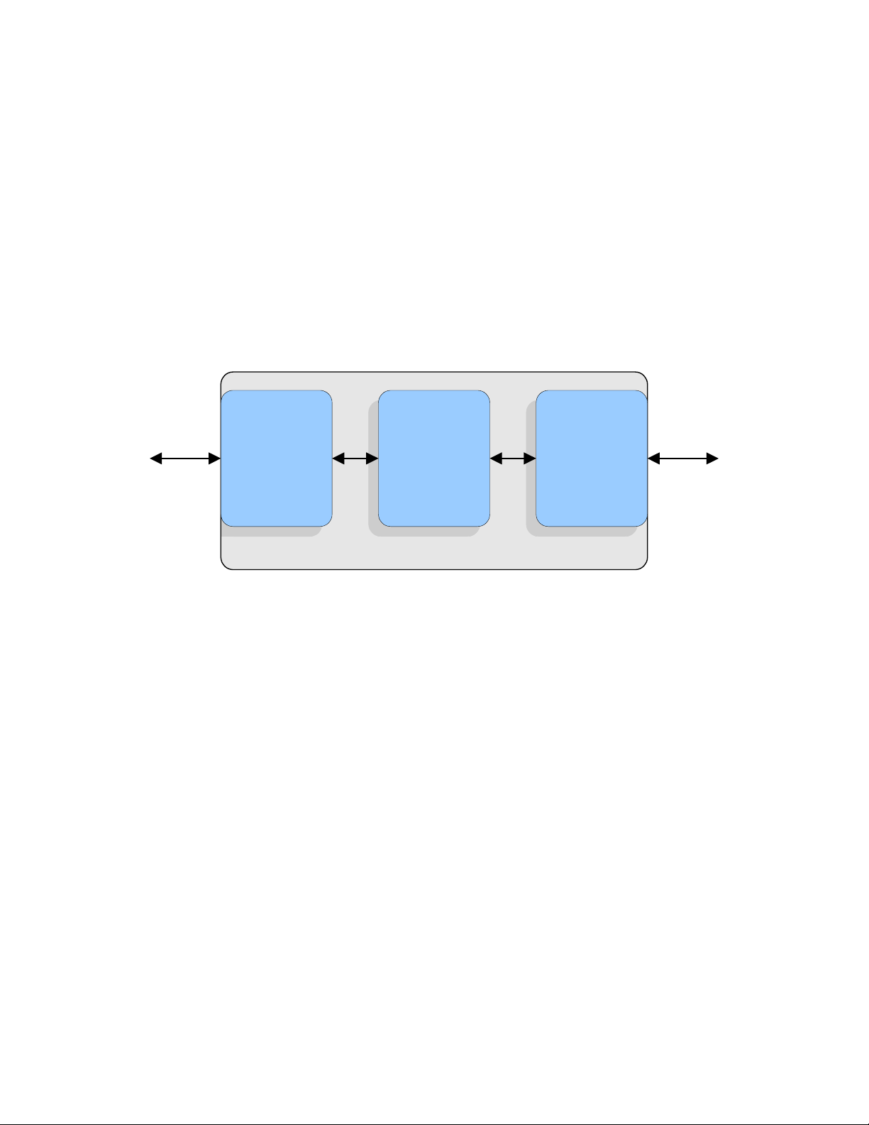
The EVB8740/EVB8741 is a PHY Evaluation Board (EVB) that interfaces a Media Independent
Interface (MII) MAC controller to the LAN8740A/LAN8741A Ethernet MII PHY via a standard 40-pin
MII connector. The LAN8740A/LAN8741A is connected to an RJ45 Ethernet jack with integrated
magnetics for 10/100 connectivity. A simplified block diagram of the EVB8740/EVB8741 can be seen
in Figure 1.1.
Figure 1.1 EVB8740/EVB8741 Block Diagram
Note: Though the LAN8740A/LAN8741A supports an RMII mode of operation, the
EVB8740/EVB8741 evaluation board does not support this mode.
1.1 References
Concepts and material available in the following documents may be helpful when reading this
document. Visit www.smsc.com for the latest documentation.
SMSC LAN8740A/LAN8741A Datasheets
AN 25.3 Migrating from the LAN8710A/LAN8720A to the LAN8740/LAN8741/LAN8742
AN 8.13 Suggested Magnetics
SMSC LAN8740A/LAN8741A Evaluation Board Schematics
Revision 1.0 (04-29-13) 2 SMSC EVB8740/EVB8741
USER MANUAL
Page 3

2 Board Details
This section includes the following EVB8740/EVB8741 board details:
Power
Configuration
Mechanicals
2.1 Power
2.1.1 +5V Power
Power is normally supplied to the EVB8740/EVB8741’s +3.3V regulator externally via the +5V power
pins of the MII connector. If desired, the EVB8740/EVB8741 can be powered without +5V present on
the MII connector by supplying +5V to the TP2 (red) test point with ground connected to the TP4
(black) test point.
Note: Before connecting an external power supply to TP2, ensure power is not present on the MII
connector’s +5V pins. Connecting +5V simultaneously via the MII connector and TP2 may
result in permanent damage to the board.
EVB8740/EVB8741 Evaluation Board User Manual
2.1.2 VDDIO Power
The LAN8740A/LAN8741A’s VDDIO power may be supplied at a voltage other than +3.3V by
depopulating resistor R12 and supplying +1.6V to +3.6V externally via test point TP5 (purple), with
ground connected to the TP4 (black) test point.
Note: Before connecting an external power supply to TP5, ensure that resistor R12 has been
removed. Connecting an external power supply to TP5 while resistor R12 is populated may
result in permanent damage to the board.
2.1.3 +1.2V Power
The LAN8740A/LAN8741A’s internal +1.2V regulator can be optionally disabled. Refer to Section 2.2.4,
"Internal +1.2V Regulator Configuration (REGOFF)," on page 6 for additional information.
SMSC EVB8740/EVB8741 3 Revision 1.0 (04-29-13)
USER MANUAL
Page 4
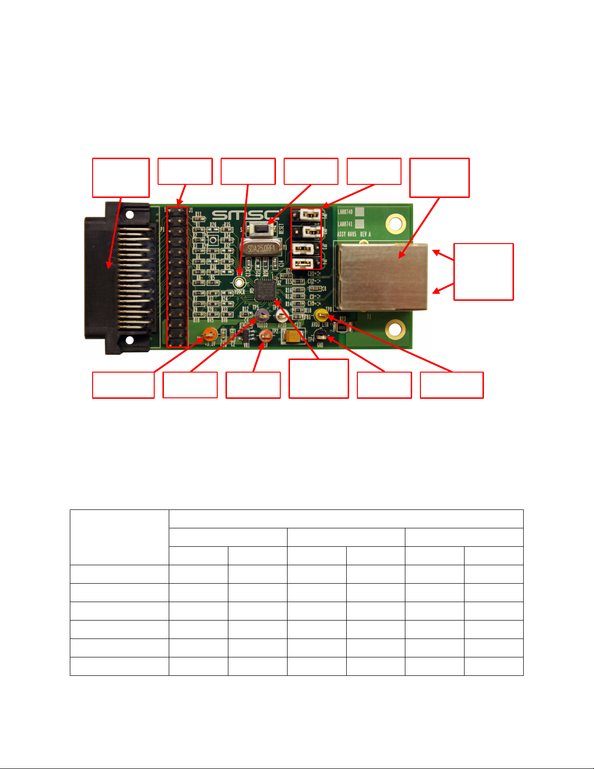
EVB8740/EVB8741 Evaluation Board User Manual
MII
Testpoints
VDDCR
Testpoint
Reset
Button
Integrated
RJ45 +
Magnetics
SPEED &
LINK/ACT
LEDs
(integrated in
magjack)
40-pin MII
connector
(P1)
VDDIO
Testpoint
+5V
Testpoint
+3.3V
Testpoint
SMSC
LAN8740A/
LAN8741A
GND
Testpoint
JP1 – JP4
AVDD_ETH
Testpoint
2.2 Configuration
The following sub-sections describe the various board features and configuration settings. A top view
of the EVB8740/EVB8741 is shown in Figure 2.1.
Figure 2.1 Top View of the EVB8740/EVB8741
2.2.1 PHY Address Configuration
The EVB8740/EVB8741 allows the user to configure the default PHY address at power-up via the
PHYAD[2:0] configuration straps. Tab l e 2 .1 details the proper configuration required for each PHY
address value. By default, all EVB8740/EVB8741 PHY address straps are configured to a value of “0”.
Table 2.1 PHYAD[2:0] Resistor Configuration
PHYAD[2:0] PULL-UP/DOWN RESISTORS
PHYAD[2:0]
000 (Default)
001
010
011
100
101
Depopulate Populate Depopulate Populate Depopulate Populate
Depopulate Populate Depopulate Populate Populate Depopulate
Depopulate Populate Populate Depopulate Depopulate Populate
Depopulate Populate Populate Depopulate Populate Depopulate
Populate Depopulate Depopulate Populate Depopulate Populate
Populate Depopulate Depopulate Populate Populate Depopulate
PHYAD2 PHYAD1 PHYAD0
R26R35R25R36R24R37
Revision 1.0 (04-29-13) 4 SMSC EVB8740/EVB8741
USER MANUAL
Page 5

EVB8740/EVB8741 Evaluation Board User Manual
Table 2.1 PHYAD[2:0] Resistor Configuration (continued)
PHYAD[2:0] PULL-UP/DOWN RESISTORS
PHYAD[2:0]
PHYAD2 PHYAD1 PHYAD0
R26R35R25R36R24R37
110
111
Populate Depopulate Populate Depopulate Depopulate Populate
Populate Depopulate Populate Depopulate Populate Depopulate
2.2.2 Reset Mode Configuration
The EVB8740/EVB8741 can be configured to reset into a specific mode of operation at power-up via
the MODE[2:0] configuration straps. Tab le 2 .2 details the proper configuration required for each mode.
By default, all EVB8740/EVB8741 MODE[2:0] straps are configured to a value of “1”.
Note: For additional details on each mode of operation, refer to the LAN8740A/LAN8741A datasheet.
Table 2.2 MODE[2:0] Resistor Configuration
MODE[2:0]
000
10BASE-T
Half Duplex
Auto-neg disabled
Depopulate Populate Depopulate Populate Depopulate Populate
MODE2 MODE1 MODE0
R28R33R29R32R30R31
MODE[2:0] PULL-UP/DOWN RESISTORS
001
10BASE-T
Full Duplex
Auto-neg disabled
010
100BASE-TX
Half Duplex
Auto-neg disabled
011
100BASE-TX
Full Duplex
Auto-neg disabled
100
100BASE-TX
Half Duplex
Auto-neg enabled
101
Repeater mode
110
Power Down mode
111 (Def ault)
All capable.
Auto-neg enabled
Depopulate Populate Depopulate Populate Populate Depopulate
Depopulate Populate Populate Depopulate Depopulate Populate
Depopulate Populate Populate Depopulate Populate Depopulate
Populate Depopulate Depopulate Populate Depopulate Populate
Populate Depopulate Depopulate Populate Populate Depopulate
Populate Depopulate Populate Depopulate Depopulate Populate
Populate Depopulate Populate Depopulate Populate Depopulate
SMSC EVB8740/EVB8741 5 Revision 1.0 (04-29-13)
USER MANUAL
Page 6

EVB8740/EVB8741 Evaluation Board User Manual
2.2.3 nINT/TXER/TXD4 Pin Configuration (nINTSEL)
The nINT, TXER, and TXD4 functions share a common LAN8740A/LAN8741A pin. This pin can
operate in two functional modes: nINT (Interrupt) Mode and TXER/TXD4 Mode. TXER is also used in
EEE mode as TXER when TXEN = 1, and LPI when TXEN = 0. The nINTSEL configuration strap is
used to select one of these two modes. The EVB8740/EVB8741 must be properly configured for each
mode as follows:
nINT Mode
Depopulate R46.
Depopulate the 2-3 positions of JP3 and JP4.
Populate the 1-2 positions of JP3 and JP4 to pull-up the nINTSEL strap (nINT mode).
TXER/TXD4 Mode (Default EVB8740/EVB8741 Mode)
Depopulate the 1-2 positions of JP3 and JP4.
Populate the 2-3 positions of JP3 and JP4 to pull-down the nINTSEL strap (TXER/TXD4 mode).
Populate R46.
Note: The nINTSEL configuration strap shares functionality with LED2. Therefore, LED2 may function
active-high or active-low depending on the nINTSEL configuration. For additional information
on the functionality of the nINT/TXER/TXD4 and LED2/nINTSEL pins, refer to the
LAN8740A/LAN8741A Datasheet and LAN8740A/LAN8741A schematics.
2.2.4 Internal +1.2V Regulator Configuration (REGOFF)
The LAN8740A/LAN8741A provides the ability to disable the internal +1.2V regulator. When the
regulator is disabled, an external +1.2V must be supplied to the VDDCR pin (via TP3). Configuration
of the internal regulator is controlled by the REGOFF configuration strap. The EVB8740/EVB8741 must
be properly configured for each mode as follows:
Internal +1.2V Regulator Enabled (Default EVB8740/EVB8741 Mode)
Depopulate the 2-3 positions of JP1 and JP2.
Populate the 1-2 positions of JP1 and JP2 to pull-down the REGOFF strap (enable regulator).
Internal +1.2V Regulator Disabled
Depopulate the 1-2 positions of JP1 and JP2.
Populate the 2-3 positions of JP1 and JP2 to pull-up the REGOFF strap (disable regulator).
Note: The REGOFF configuration strap shares functionality with LED1. Therefore, LED1 may
function active-high or active-low depending on the REGOFF configuration. For additional
information on the LED1/REGOFF pin and the disabling of the internal 1.2V regulator (power
sequencing requirements, etc.), refer to the LAN8740A/LAN8741A Datasheet and
LAN8740A/LAN8741A schematics.
2.2.5 Clock Configuration
The EVB8740/EVB8741 can be clocked via the onboard crystal oscillator or an optional external clock.
Crystal Oscillator (Default)
The 25 MHz crystal Y1 is connected to the internal oscillator of the LAN8740A/LAN8741A. A PLL
circuit in the LAN8740A/LAN8741A generates all the timing required by the PHY.
Revision 1.0 (04-29-13) 6 SMSC EVB8740/EVB8741
USER MANUAL
Page 7

EVB8740/EVB8741 Evaluation Board User Manual
External Clock
The EVB8740/EVB8741 can be configured to use an external clock by removing crystal Y1 and resistor
R20. A 25MHz +3.3V signal may then be applied to pin 1 of Y1 (which connects to pin 5 of the
LAN8740A/LAN8741A). Pin 2 of Y1 (which connects to pin 4 of the LAN8740A/LAN8741A) should be
left floating when using an external clock.
2.2.6 LEDs
Table 2.3 LEDs
REFERENCE COLOR INDICATION
Link/Activity
LED1 Green
LED2 Yellow
Active when the PHY has established a valid link with a link partner
and blinks when activity is detected.
Speed
Active when a 100BASE-TX link has been established. Inactive when
a 10BASE-T link has been established or during line isolation.
Note: LED1 and LED2 are located inside the RJ45 connector. LED1 and LED2 may function active-
high or active-low depending on the configuration of the REGOFF and nINTSEL straps,
respectively. Refer to the LAN8740A/LAN8741A Datasheet and LAN8740A/LAN8741A
schematics for additional information.
2.2.7 Test Points
Table 2.4 Test Points
TEST POINT DESCRIPTION CONNECTION
TP1 +3.3V Test Point (Orange) +3.3V
TP2 +5.0V Test Point (Red) +5.0V
TP3
TP4 Ground Test Point (Black) Ground
TP5 VDDIO Test Point (Purple) +3.3V (Note 2.2)
TP6 nPME Test Point (Unpopulated) nPME (RXD2/nPME/RMIISEL)
TP7 AVDD Test Point (White) AVDD
TP8 AVDD_ETH Test Point (Yellow) AVDD_ETH
+1.2V VDDCR Test Point (Unpopulated)
(Note 2.1)
+1.2V
Note 2.1 VDDCR is the internal +1.2V regulated output. When REGOFF is enabled, the internal
1.2V regulator is disabled. In this case, an external 1.2V regulator must be supplied to test
point TP3.
Note 2.2 The LAN8740A/LAN8741A’s VDDIO power may be supplied externally at a voltage other
than +3.3V as described in Section 2.1, "Power," on page 3.
SMSC EVB8740/EVB8741 7 Revision 1.0 (04-29-13)
USER MANUAL
Page 8

EVB8740/EVB8741 Evaluation Board User Manual
2.2.8 System Connections
Table 2.5 System Connections
PLUG/HEADER DESCRIPTION PART
T1 RJ45 with Integrated LEDs Pulse J0011D01BNL
J1
P1
HEADER
PIN DESCRIPTION
1nRST 15TXD1
2MDIO (Note 2.3)16TXD2
3MDC 17TXD3
4 RXD3/PHYAD2
5 RXD2/RMIISEL 19 CRS
6RXD1/MODE1
7RXD0/MODE0
8 RXDV 22 VDDIO
2x14 MII Header
Note: Refer Table 2.6 to for a full pin list
40-pin Female MII Connector
Note: Refer Table 2.7 to for a full pin list
Table 2.6 J1 - 2x14 MII Header Pinout
HEADER
PIN DESCRIPTION
18 CRS_DV/COL/MODE2
20 Ground
21 nINT (Note 2.4)
Adam Tech PH2-28-U-A
Tyco 5173278-2
9 RXCLK/PHYAD1 23 +3.3V
10 RXER/RXD4/PHYAD0
11 TXER/TXD4 (Note 2.4) 25 Ground
12 TXCLK 26 Ground
13 TXEN 27 Ground
14 TXD0 28 Ground
Note 2.3 Resistor R11 acts as a pull-up on the MDIO pin. In most situations, the MAC circuitry
provides this pull-up and R11 is not required.
Note 2.4 Pins 11 and 21 of the J1 header must be configured to properly connect to the
nINT/TXER/TXD4 pin of the LAN8740A/LAN8741A. Depending on the configured mode,
nINT or TXER/TXD4, R46 must be depopulated or populated. Refer to Section 2.2.3,
"nINT/TXER/TXD4 Pin Configuration (nINTSEL)," on page 6 for additional information.
Revision 1.0 (04-29-13) 8 SMSC EVB8740/EVB8741
24 Ground
USER MANUAL
Page 9

EVB8740/EVB8741 Evaluation Board User Manual
Table 2.7 P1 - 40-Pin Female MII Connector Pinout
PIN DESCRIPTION PIN DESCRIPTION PIN DESCRIPTION PIN DESCRIPTION
1 +5V 11 TXER
2 MDIO 12 TXCLK 22 GND 32 GND
3 MDC 13 TXEN 23 GND 33 GND
4 RXD3 14 TXD0 24 GND 34 GND
5 RXD2 15 TXD1 25 GND 35 GND
6 RXD1 16 TXD2 26 GND 36 GND
7 RXD0 17 TXD3 27 GND 37 GND
8 RXDV 18 COL 28 GND 38 GND
9 RXCLK 19 CRS 29 GND 39 GND
10 RXER 20 +5V 30 GND 40 +5V
Note 2.5 To use the TXER signal from the MAC, the nINT/TXER/TXD4 pin and R46 must be
configured properly. Refer to Section 2.2.3, "nINT/TXER/TXD4 Pin Configuration
(nINTSEL)," on page 6 for additional information.
(Note 2.5) 21 +5V 31 GND
2.2.9 Switches
Table 2.8 Switches
SWITCH DESCRIPTION FUNCTION
S1 Reset switch When pressed, triggers a board reset.
SMSC EVB8740/EVB8741 9 Revision 1.0 (04-29-13)
USER MANUAL
Page 10

EVB8740/EVB8741 Evaluation Board User Manual
1.450
3.000
Ø0.125
Ø0.125
TOP VIEW
0.200
0.175
0.200
0.175
2.3 Mechanicals
Figure 2.2 details the EVB8740/EVB8741 mechanical dimensions.
Figure 2.2 EVB8740/EVB8741 Mechanicals
Revision 1.0 (04-29-13) 10 SMSC EVB8740/EVB8741
USER MANUAL
Page 11

EVB8740/EVB8741 Evaluation Board User Manual
3 User Manual Revision History
Table 3.1 Customer Revision History
REVISION LEVEL & DATE SECTION/FIGURE/ENTRY CORRECTION
Rev. 1.0 (04-29-13) All Initial release.
SMSC EVB8740/EVB8741 11 Revision 1.0 (04-29-13)
USER MANUAL
Page 12

Mouser Electronics
Authorized Distributor
Click to View Pricing, Inventory, Delivery & Lifecycle Information:
Microchip:
EVB8740
 Loading...