

Page 1

EMC1403/EMC1404
1°C Temperature Sensor with Beta Compensation
PRODUCT FEATURES
General Description
The EMC1403 and EMC1404 are high accuracy, low
cost, System Management Bus (SMBus) temperature
sensors. Advanced features such as Resistance Error
Correction (REC), Beta Compensation (to support CPU
diodes requiring the BJT/transistor model including
45nm, 65nm and 90nm processors) and automatic
diode type detection combine to provide a robust
solution for complex environmental monitoring
applications.
Each device provides ±1° accuracy for external diode
temperatures and ±2°C accuracy for the internal diode
temperature. The EMC1403 monitors three temperature
channels (two external and one internal). The EMC1404
monitors four temperature channels (three external and
one internal).
Resistance Error Correction automatically eliminates the
temperature error caused by series resistance allowing
greater flexibility in routing thermal diodes. Beta
Compensation eliminates temperature errors caused by
low, variable beta transistors common in today's fine
geometry processors. The automatic beta detection
feature monitors each external diode/transistor and
determines the optimum sensor settings for accurate
temperature measurements regardless of processor
technology. This frees the user from providing unique
sensor configurations for each temperature monitoring
application. These advanced features plus ±1°C
measurement accuracy provide a low-cost, highly
flexible and accurate solution for critical temperature
monitoring applications.
Data Sheet
Applications
Notebook Computers
Desktop Computers
Industrial
Embedded applications
Features
Support for diodes requiring the BJT/transistor model
— supports 45nm, 65nm, and 90nm CPU thermal diodes.
Automatically determines external diode type and
optimal settings
Resistance Error Correction
External Temperature Monitors
— ±1°C Accuracy (60°C < T
— 0.125°C Resolution
— Anti-parallel diodes for extra diode support
Internal Temperature Monitor
— ±2°C accuracy
3.3V Supply Voltage
Programmable temperature limits for ALERT and
THERM
Available in these RoHS Compliant Packages
— 10-pin 3mm x 3mm DFN
— 10-pin MSOP
— 14-pin SOIC
DIODE
< 100°C)
2014 Microchip Technology Inc. DS20005272A-page 1
Page 2

1°C Temperature Sensor with Beta Compensation
Ordering Information:
EMC1403-1-AIZL-TR for 10-pin, MSOP RoHS Compliant Package
EMC1403-2-AIZL-TR for 10-pin, MSOP RoHS Compliant Package
EMC1403-3-AIZL-TR for 10-pin, MSOP RoHS Compliant Package
EMC1403-4-AIZL-TR for 10-pin, MSOP RoHS Compliant Package
EMC1403-1-AIA-TR for 10-pin, DFN RoHS Compliant Package
EMC1403-2-AIA-TR for 10-pin, DFN RoHS Compliant Package
EMC1403-3-AIA-TR for 10-pin, DFN RoHS Compliant Package
EMC1403-4-AIA-TR for 10-pin, DFN RoHS Compliant Package
EMC1403-1-YZT-TR for 14-pin, SOIC RoHS Compliant Package
EMC1403-2-YZt-TR for 14-pin, SOIC RoHS Compliant Package
EMC1403-3-YZt-TR for 14-pin, SOIC RoHS Compliant Package
EMC1403-4-YZt-TR for 14-pin, SOIC RoHS Compliant Package
EMC1404-1-AIZL-TR for 10-pin, MSOP RoHS Compliant Package
EMC1404-2-AIZL-TR for 10-pin, MSOP RoHS Compliant Package
EMC1404-3-AIZL-TR for 10-pin, MSOP RoHS Compliant Package
EMC1404-4-AIZL-TR for 10-pin, MSOP RoHS Compliant Package
Note: See Table 1.1, "Part Selection" for SMBus addressing options.
REEL SIZE IS 4,000 PIECES.
This product meets the halogen maximum concentration values per IEC61249-2-21
Data Sheet
TO OUR VALUED CUSTOMERS
It is our intention to provide our valued customers with the best documentation possible to ensure successful use of your Microchip
products. To this end, we will continue to improve our publications to better suit your needs. Our publications will be refined and
enhanced as new volumes and updates are introduced.
If you have any questions or comments regarding this publication, please contact the Marketing Communications Department via
E-mail at docerrors@microchip.com. We welcome your feedback.
Most Current Data Sheet
To obtain the most up-to-date version of this data sheet, please register at our Worldwide Web site at:
http://www.microchip.com
You can determine the version of a data sheet by examining its literature number found on the bottom outside corner of any page.
The last character of the literature number is the version number, (e.g., DS30000000A is version A of document DS30000000).
Errata
An errata sheet, describing minor operational differences from the data sheet and recommended workarounds, may exist for current devices. As device/documentation issues become known to us, we will publish an errata sheet. The errata will specify the revision of silicon and revision of document to which it applies.
To determine if an errata sheet exists for a particular device, please check with one of the following:
• Microchip’s Worldwide Web site; http://www.microchip.com
• Your local Microchip sales office (see last page)
When contacting a sales office, please specify which device, revision of silicon and data sheet (include -literature number) you are
using.
Customer Notification System
Register on our web site at www.microchip.com to receive the most current information on all of our products.
DS20005272A-page 2 2014 Microchip Technology Inc.
Page 3

1°C Temperature Sensor with Beta Compensation
Data Sheet
Table of Contents
Chapter 1 Block Diagram . . . . . . . . . . . . . . . . . . . . . . . . . . . . . . . . . . . . . . . . . . . . . . . . . . . . . 7
1.1 Part Selection . . . . . . . . . . . . . . . . . . . . . . . . . . . . . . . . . . . . . . . . . . . . . . . . . . . . . . . . . . . . . . . . . . 7
Chapter 2 Pin Description. . . . . . . . . . . . . . . . . . . . . . . . . . . . . . . . . . . . . . . . . . . . . . . . . . . . . 9
Chapter 3 Electrical Specifications. . . . . . . . . . . . . . . . . . . . . . . . . . . . . . . . . . . . . . . . . . . . . 11
3.1 Absolute Maximum Ratings . . . . . . . . . . . . . . . . . . . . . . . . . . . . . . . . . . . . . . . . . . . . . . . . . . . . . . 11
3.2 Electrical Specifications . . . . . . . . . . . . . . . . . . . . . . . . . . . . . . . . . . . . . . . . . . . . . . . . . . . . . . . . . 12
3.3 SMBus Electrical Characteristics . . . . . . . . . . . . . . . . . . . . . . . . . . . . . . . . . . . . . . . . . . . . . . . . . . 13
Chapter 4 System Management Bus Interface Protocol . . . . . . . . . . . . . . . . . . . . . . . . . . . 14
4.1 System Management Bus Interface Protocol . . . . . . . . . . . . . . . . . . . . . . . . . . . . . . . . . . . . . . . . . 14
4.2 Write Byte . . . . . . . . . . . . . . . . . . . . . . . . . . . . . . . . . . . . . . . . . . . . . . . . . . . . . . . . . . . . . . . . . . . . 15
4.3 Read Byte . . . . . . . . . . . . . . . . . . . . . . . . . . . . . . . . . . . . . . . . . . . . . . . . . . . . . . . . . . . . . . . . . . . . 15
4.4 Send Byte . . . . . . . . . . . . . . . . . . . . . . . . . . . . . . . . . . . . . . . . . . . . . . . . . . . . . . . . . . . . . . . . . . . . 15
4.5 Receive Byte. . . . . . . . . . . . . . . . . . . . . . . . . . . . . . . . . . . . . . . . . . . . . . . . . . . . . . . . . . . . . . . . . . 15
4.6 Alert Response Address . . . . . . . . . . . . . . . . . . . . . . . . . . . . . . . . . . . . . . . . . . . . . . . . . . . . . . . . . 16
4.7 SMBus Address . . . . . . . . . . . . . . . . . . . . . . . . . . . . . . . . . . . . . . . . . . . . . . . . . . . . . . . . . . . . . . . 16
4.8 SMBus Timeout . . . . . . . . . . . . . . . . . . . . . . . . . . . . . . . . . . . . . . . . . . . . . . . . . . . . . . . . . . . . . . . 16
Chapter 5 Product Description. . . . . . . . . . . . . . . . . . . . . . . . . . . . . . . . . . . . . . . . . . . . . . . . 17
5.1 Modes of Operation . . . . . . . . . . . . . . . . . . . . . . . . . . . . . . . . . . . . . . . . . . . . . . . . . . . . . . . . . . . . 18
5.1.1 Conversion Rates . . . . . . . . . . . . . . . . . . . . . . . . . . . . . . . . . . . . . . . . . . . . . . . . . . . . . . 18
5.1.2 Dynamic Averaging . . . . . . . . . . . . . . . . . . . . . . . . . . . . . . . . . . . . . . . . . . . . . . . . . . . . . 18
5.2 THERM Output . . . . . . . . . . . . . . . . . . . . . . . . . . . . . . . . . . . . . . . . . . . . . . . . . . . . . . . . . . . . . . . . 20
5.3 ALERT Output . . . . . . . . . . . . . . . . . . . . . . . . . . . . . . . . . . . . . . . . . . . . . . . . . . . . . . . . . . . . . . . . 20
5.3.1 ALERT Pin Interrupt Mode. . . . . . . . . . . . . . . . . . . . . . . . . . . . . . . . . . . . . . . . . . . . . . . . 20
5.3.2 ALERT Pin Comparator Mode. . . . . . . . . . . . . . . . . . . . . . . . . . . . . . . . . . . . . . . . . . . . . 20
5.4 Beta Compensation . . . . . . . . . . . . . . . . . . . . . . . . . . . . . . . . . . . . . . . . . . . . . . . . . . . . . . . . . . . . 21
5.5 Resistance Error Correction (REC) . . . . . . . . . . . . . . . . . . . . . . . . . . . . . . . . . . . . . . . . . . . . . . . . 21
5.6 Programmable External Diode Ideality Factor . . . . . . . . . . . . . . . . . . . . . . . . . . . . . . . . . . . . . . . . 21
5.7 Diode Faults . . . . . . . . . . . . . . . . . . . . . . . . . . . . . . . . . . . . . . . . . . . . . . . . . . . . . . . . . . . . . . . . . . 21
5.8 Consecutive Alerts . . . . . . . . . . . . . . . . . . . . . . . . . . . . . . . . . . . . . . . . . . . . . . . . . . . . . . . . . . . . . 22
5.9 Digital Filter. . . . . . . . . . . . . . . . . . . . . . . . . . . . . . . . . . . . . . . . . . . . . . . . . . . . . . . . . . . . . . . . . . . 22
5.10 Temperature Monitors . . . . . . . . . . . . . . . . . . . . . . . . . . . . . . . . . . . . . . . . . . . . . . . . . . . . . . . . . . 23
5.11 Temperature Measurement Results and Data . . . . . . . . . . . . . . . . . . . . . . . . . . . . . . . . . . . . . . . . 24
5.12 Anti-parallel Diode Connections . . . . . . . . . . . . . . . . . . . . . . . . . . . . . . . . . . . . . . . . . . . . . . . . . . . 25
5.13 External Diode Connections . . . . . . . . . . . . . . . . . . . . . . . . . . . . . . . . . . . . . . . . . . . . . . . . . . . . . . 25
Chapter 6 Register Description. . . . . . . . . . . . . . . . . . . . . . . . . . . . . . . . . . . . . . . . . . . . . . . . 27
6.1 Data Read Interlock . . . . . . . . . . . . . . . . . . . . . . . . . . . . . . . . . . . . . . . . . . . . . . . . . . . . . . . . . . . . 30
6.2 Temperature Data Registers . . . . . . . . . . . . . . . . . . . . . . . . . . . . . . . . . . . . . . . . . . . . . . . . . . . . . 30
6.3 Status Register . . . . . . . . . . . . . . . . . . . . . . . . . . . . . . . . . . . . . . . . . . . . . . . . . . . . . . . . . . . . . . . . 31
6.4 Configuration Register . . . . . . . . . . . . . . . . . . . . . . . . . . . . . . . . . . . . . . . . . . . . . . . . . . . . . . . . . . 31
6.5 Conversion Rate Register. . . . . . . . . . . . . . . . . . . . . . . . . . . . . . . . . . . . . . . . . . . . . . . . . . . . . . . . 32
6.6 Limit Registers . . . . . . . . . . . . . . . . . . . . . . . . . . . . . . . . . . . . . . . . . . . . . . . . . . . . . . . . . . . . . . . . 33
6.7 Scratchpad Registers . . . . . . . . . . . . . . . . . . . . . . . . . . . . . . . . . . . . . . . . . . . . . . . . . . . . . . . . . . . 35
6.8 One Shot Register . . . . . . . . . . . . . . . . . . . . . . . . . . . . . . . . . . . . . . . . . . . . . . . . . . . . . . . . . . . . . 35
6.9 Therm Limit Registers. . . . . . . . . . . . . . . . . . . . . . . . . . . . . . . . . . . . . . . . . . . . . . . . . . . . . . . . . . . 35
6.10 External Diode Fault Register. . . . . . . . . . . . . . . . . . . . . . . . . . . . . . . . . . . . . . . . . . . . . . . . . . . . . 36
2014 Microchip Technology Inc. DS20005272A-page 3
Page 4

1°C Temperature Sensor with Beta Compensation
Data Sheet
6.11 Channel Mask Register . . . . . . . . . . . . . . . . . . . . . . . . . . . . . . . . . . . . . . . . . . . . . . . . . . . . . . . . . 36
6.12 Consecutive ALERT Register . . . . . . . . . . . . . . . . . . . . . . . . . . . . . . . . . . . . . . . . . . . . . . . . . . . . . 37
6.13 Beta Configuration Registers . . . . . . . . . . . . . . . . . . . . . . . . . . . . . . . . . . . . . . . . . . . . . . . . . . . . . 38
6.14 External Diode Ideality Factor Registers . . . . . . . . . . . . . . . . . . . . . . . . . . . . . . . . . . . . . . . . . . . . 39
6.15 High Limit Status Register . . . . . . . . . . . . . . . . . . . . . . . . . . . . . . . . . . . . . . . . . . . . . . . . . . . . . . . 41
6.16 Low Limit Status Register . . . . . . . . . . . . . . . . . . . . . . . . . . . . . . . . . . . . . . . . . . . . . . . . . . . . . . . . 41
6.17 THERM Limit Status Register. . . . . . . . . . . . . . . . . . . . . . . . . . . . . . . . . . . . . . . . . . . . . . . . . . . . . 42
6.18 Filter Control Register. . . . . . . . . . . . . . . . . . . . . . . . . . . . . . . . . . . . . . . . . . . . . . . . . . . . . . . . . . . 42
6.19 Product ID Register . . . . . . . . . . . . . . . . . . . . . . . . . . . . . . . . . . . . . . . . . . . . . . . . . . . . . . . . . . . . 43
6.20 Microchip ID Register (FEh) . . . . . . . . . . . . . . . . . . . . . . . . . . . . . . . . . . . . . . . . . . . . . . . . . . . . . . 43
6.21 Revision Register (FFh) . . . . . . . . . . . . . . . . . . . . . . . . . . . . . . . . . . . . . . . . . . . . . . . . . . . . . . . . . 44
Chapter 7 Typical Operating Curves. . . . . . . . . . . . . . . . . . . . . . . . . . . . . . . . . . . . . . . . . . . 45
Chapter 8 Package Information . . . . . . . . . . . . . . . . . . . . . . . . . . . . . . . . . . . . . . . . . . . . . . . 47
8.1 Package Markings . . . . . . . . . . . . . . . . . . . . . . . . . . . . . . . . . . . . . . . . . . . . . . . . . . . . . . . . . . . . . 51
8.1.1 EMC1404-X-AIZL (10-pin MSOP) . . . . . . . . . . . . . . . . . . . . . . . . . . . . . . . . . . . . . . . . . . 51
8.1.2 EMC1403-X-AIZL (10-pin MSOP) . . . . . . . . . . . . . . . . . . . . . . . . . . . . . . . . . . . . . . . . . . 51
8.1.3 EMC1403-1-AIA and EMC1403-2-AIA (10-pin DFN). . . . . . . . . . . . . . . . . . . . . . . . . . . . 51
8.1.4 EMC1403-YZT. . . . . . . . . . . . . . . . . . . . . . . . . . . . . . . . . . . . . . . . . . . . . . . . . . . . . . . . . 51
Chapter 9 Data Sheet Revision History . . . . . . . . . . . . . . . . . . . . . . . . . . . . . . . . . . . . . . . . . 52
DS20005272A-page 4 2014 Microchip Technology Inc.
Page 5

1°C Temperature Sensor with Beta Compensation
Data Sheet
List of Figures
Figure 1.1 EMC1403/EMC1404 Block Diagram . . . . . . . . . . . . . . . . . . . . . . . . . . . . . . . . . . . . . . . . . . . . 7
Figure 2.1 EMC1403/EMC1404 Pin Diagram, MSOP-10 . . . . . . . . . . . . . . . . . . . . . . . . . . . . . . . . . . . . . 9
Figure 2.2 EMC1403/EMC1404 Pin Diagram, DFN-10. . . . . . . . . . . . . . . . . . . . . . . . . . . . . . . . . . . . . . . 9
Figure 2.3 EMC1403/EMC1404 Pin Diagram, SOIC-14 . . . . . . . . . . . . . . . . . . . . . . . . . . . . . . . . . . . . . . 9
Figure 4.1 SMBus Timing Diagram . . . . . . . . . . . . . . . . . . . . . . . . . . . . . . . . . . . . . . . . . . . . . . . . . . . . . 14
Figure 5.1 System Diagram for EMC1403 . . . . . . . . . . . . . . . . . . . . . . . . . . . . . . . . . . . . . . . . . . . . . . . 17
Figure 5.2 System Diagram for EMC1404 . . . . . . . . . . . . . . . . . . . . . . . . . . . . . . . . . . . . . . . . . . . . . . . 18
Figure 5.3 Temperature Filter Step Response . . . . . . . . . . . . . . . . . . . . . . . . . . . . . . . . . . . . . . . . . . . . 22
Figure 5.4 Temperature Filter Impulse Response. . . . . . . . . . . . . . . . . . . . . . . . . . . . . . . . . . . . . . . . . . 23
Figure 5.5 Block Diagram of Temperature Monitoring Circuit . . . . . . . . . . . . . . . . . . . . . . . . . . . . . . . . . 24
Figure 5.6 Diode Configurations . . . . . . . . . . . . . . . . . . . . . . . . . . . . . . . . . . . . . . . . . . . . . . . . . . . . . . . 26
Figure 8.1 10-Pin MSOP / TSSOP Package . . . . . . . . . . . . . . . . . . . . . . . . . . . . . . . . . . . . . . . . . . . . . . 47
Figure 8.2 10-Pin DFN Package Drawing (1 of 2). . . . . . . . . . . . . . . . . . . . . . . . . . . . . . . . . . . . . . . . . . 48
Figure 8.3 10-Pin DFN Package Dimensions (2 of 2) . . . . . . . . . . . . . . . . . . . . . . . . . . . . . . . . . . . . . . . 49
Figure 8.4 Package Drawing and PCB Footprint for SOIC-14 . . . . . . . . . . . . . . . . . . . . . . . . . . . . . . . . 50
2014 Microchip Technology Inc. DS20005272A-page 5
Page 6

1°C Temperature Sensor with Beta Compensation
Data Sheet
List of Tables
Table 1.1 Part Selection . . . . . . . . . . . . . . . . . . . . . . . . . . . . . . . . . . . . . . . . . . . . . . . . . . . . . . . . . . . . . . 7
Table 2.1 EMC1403 and EMC1404 Pin Description . . . . . . . . . . . . . . . . . . . . . . . . . . . . . . . . . . . . . . . . 10
Table 3.1 Absolute Maximum Ratings . . . . . . . . . . . . . . . . . . . . . . . . . . . . . . . . . . . . . . . . . . . . . . . . . . . 11
Table 3.2 Electrical Specifications . . . . . . . . . . . . . . . . . . . . . . . . . . . . . . . . . . . . . . . . . . . . . . . . . . . . . . 12
Table 3.3 SMBus Electrical Specifications . . . . . . . . . . . . . . . . . . . . . . . . . . . . . . . . . . . . . . . . . . . . . . . 13
Table 4.1 Protocol Format . . . . . . . . . . . . . . . . . . . . . . . . . . . . . . . . . . . . . . . . . . . . . . . . . . . . . . . . . . . . 14
Table 4.2 Write Byte Protocol . . . . . . . . . . . . . . . . . . . . . . . . . . . . . . . . . . . . . . . . . . . . . . . . . . . . . . . . . 15
Table 4.3 Read Byte Protocol . . . . . . . . . . . . . . . . . . . . . . . . . . . . . . . . . . . . . . . . . . . . . . . . . . . . . . . . . 15
Table 4.4 Send Byte Protocol . . . . . . . . . . . . . . . . . . . . . . . . . . . . . . . . . . . . . . . . . . . . . . . . . . . . . . . . . 15
Table 4.5 Receive Byte Protocol . . . . . . . . . . . . . . . . . . . . . . . . . . . . . . . . . . . . . . . . . . . . . . . . . . . . . . . 15
Table 4.6 Alert Response Address Protocol . . . . . . . . . . . . . . . . . . . . . . . . . . . . . . . . . . . . . . . . . . . . . . 16
Table 5.1 Supply Current vs. Conversion Rate for EMC1403 . . . . . . . . . . . . . . . . . . . . . . . . . . . . . . . . . 19
Table 5.2 Supply Current vs. Conversion Rate for EMC1404 . . . . . . . . . . . . . . . . . . . . . . . . . . . . . . . . . 19
Table 5.3 Temperature Data Format . . . . . . . . . . . . . . . . . . . . . . . . . . . . . . . . . . . . . . . . . . . . . . . . . . . . 24
Table 6.1 Register Set in Hexadecimal Order . . . . . . . . . . . . . . . . . . . . . . . . . . . . . . . . . . . . . . . . . . . . . 27
Table 6.2 Temperature Data Registers . . . . . . . . . . . . . . . . . . . . . . . . . . . . . . . . . . . . . . . . . . . . . . . . . . 30
Table 6.3 Status Register . . . . . . . . . . . . . . . . . . . . . . . . . . . . . . . . . . . . . . . . . . . . . . . . . . . . . . . . . . . . 31
Table 6.4 Configuration Register . . . . . . . . . . . . . . . . . . . . . . . . . . . . . . . . . . . . . . . . . . . . . . . . . . . . . . . 31
Table 6.5 Conversion Rate Register . . . . . . . . . . . . . . . . . . . . . . . . . . . . . . . . . . . . . . . . . . . . . . . . . . . . 32
Table 6.6 Conversion Rate . . . . . . . . . . . . . . . . . . . . . . . . . . . . . . . . . . . . . . . . . . . . . . . . . . . . . . . . . . . 33
Table 6.7 Temperature Limit Registers . . . . . . . . . . . . . . . . . . . . . . . . . . . . . . . . . . . . . . . . . . . . . . . . . . 33
Table 6.8 Scratchpad Register . . . . . . . . . . . . . . . . . . . . . . . . . . . . . . . . . . . . . . . . . . . . . . . . . . . . . . . . 35
Table 6.9 One Shot Register . . . . . . . . . . . . . . . . . . . . . . . . . . . . . . . . . . . . . . . . . . . . . . . . . . . . . . . . . . 35
Table 6.10 Therm Limit Registers . . . . . . . . . . . . . . . . . . . . . . . . . . . . . . . . . . . . . . . . . . . . . . . . . . . . . . . 35
Table 6.11 External Diode Fault Register . . . . . . . . . . . . . . . . . . . . . . . . . . . . . . . . . . . . . . . . . . . . . . . . . 36
Table 6.12 Channel Mask Register . . . . . . . . . . . . . . . . . . . . . . . . . . . . . . . . . . . . . . . . . . . . . . . . . . . . . . 36
Table 6.13 Consecutive ALERT Register . . . . . . . . . . . . . . . . . . . . . . . . . . . . . . . . . . . . . . . . . . . . . . . . . 37
Table 6.14 Consecutive Alert / THERM Settings. . . . . . . . . . . . . . . . . . . . . . . . . . . . . . . . . . . . . . . . . . . . 38
Table 6.15 Beta Configuration Registers. . . . . . . . . . . . . . . . . . . . . . . . . . . . . . . . . . . . . . . . . . . . . . . . . . 38
Table 6.16 CPU Beta Values. . . . . . . . . . . . . . . . . . . . . . . . . . . . . . . . . . . . . . . . . . . . . . . . . . . . . . . . . . . 39
Table 6.17 Ideality Configuration Registers. . . . . . . . . . . . . . . . . . . . . . . . . . . . . . . . . . . . . . . . . . . . . . . . 39
Table 6.18 Ideality Factor Look-Up Table (Diode Model) . . . . . . . . . . . . . . . . . . . . . . . . . . . . . . . . . . . . . 40
Table 6.19 Substrate Diode Ideality Factor Look-Up Table (BJT Model) . . . . . . . . . . . . . . . . . . . . . . . . . 40
Table 6.20 High Limit Status Register . . . . . . . . . . . . . . . . . . . . . . . . . . . . . . . . . . . . . . . . . . . . . . . . . . . . 41
Table 6.21 Low Limit Status Register . . . . . . . . . . . . . . . . . . . . . . . . . . . . . . . . . . . . . . . . . . . . . . . . . . . . 41
Table 6.22 THERM Limit Status Register . . . . . . . . . . . . . . . . . . . . . . . . . . . . . . . . . . . . . . . . . . . . . . .
Table 6.23 Filter Configuration Register . . . . . . . . . . . . . . . . . . . . . . . . . . . . . . . . . . . . . . . . . . . . . . . . . . 42
Table 6.24 Filter Settings. . . . . . . . . . . . . . . . . . . . . . . . . . . . . . . . . . . . . . . . . . . . . . . . . . . . . . . . . . . . . . 43
Table 6.25 Product ID Register . . . . . . . . . . . . . . . . . . . . . . . . . . . . . . . . . . . . . . . . . . . . . . . . . . . . . . . . . 43
Table 6.26 Manufacturer ID Register. . . . . . . . . . . . . . . . . . . . . . . . . . . . . . . . . . . . . . . . . . . . . . . . . . . . . 43
Table 6.27 Revision Register. . . . . . . . . . . . . . . . . . . . . . . . . . . . . . . . . . . . . . . . . . . . . . . . . . . . . . . . . . . 44
Table 9.1 Revision History. . . . . . . . . . . . . . . . . . . . . . . . . . . . . . . . . . . . . . . . . . . . . . . . . . . . . . . . . . . . 52
. . 42
DS20005272A-page 6 2014 Microchip Technology Inc.
Page 7
1°C Temperature Sensor with Beta Compensation
Data Sheet
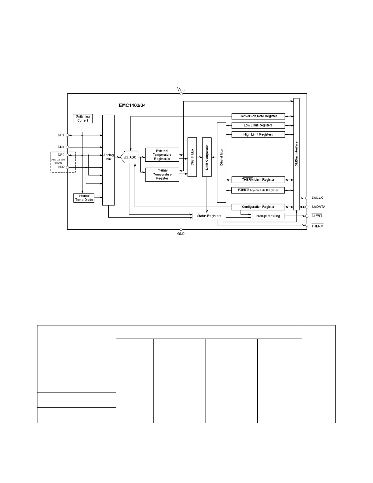
Chapter 1 Block Diagram
Figure 1.1 EMC1403/EMC1404 Block Diagram
1.1 Part Selection
The EMC1403 and EMC1404 device configuration is highlighted below.
PART
NUMBER
EMC1403 - 1 -
AIZL
EMC1403 - 2 -
AIZL
EMC1403 - 3 -
AIZL
EMC1403 - 4 -
AIZL
SMBUS
ADDRESS
1001_100xb
1001_101xb
0011_000xb
0101_001xb
EXTERNAL
DIODES
Table 1.1 Part Selection
FUNCTIONALITY
DIODE 1
DEFAULT
CONFIGURATION
2
Detect Diode w/ REC
enabled
DIODE 2
DEFAULT
CONFIGURATION OTHER
Software program-
mable and mas-
Detect Diode w/ REC
enabled
kable High Limits
Software program-
mable THERM
Limits
PRODUCT
ID
21h
2014 Microchip Technology Inc. DS20005272A-page 7
Page 8

1°C Temperature Sensor with Beta Compensation
Table 1.1 Part Selection (continued)
FUNCTIONALITY
Data Sheet
PART
NUMBER
EMC1403 - 1 -
AIA
EMC1403 - 2 -
AIA
EMC1403 - 3 -
AIA
EMC1403 - 4 -
AIA
EMC1403 - 1 -
YZT
EMC1403 - 2 -
YZT
EMC1403 - 3 -
YZT
EMC1403 - 4 -
YZT
EMC1404 - 1 1001_100xb
EMC1404 - 2 1001_101xb
EMC1404 - 3 0011_000xb
EMC1404 - 4 0101_001xb
SMBUS
ADDRESS
1001_100xb
1001_101xb
0011_000xb
0101_001xb
1001_100xb
1001_101xb
0011_000xb
0101_001xb
EXTERNAL
DIODES
2
2
3
DIODE 1
DEFAULT
CONFIGURATION
Detect Diode w/ REC
enabled
Detect Diode w/ REC
enabled
Detect Diode w/ REC
enabled
DIODE 2
DEFAULT
CONFIGURATION OTHER
Software program-
mable and mas-
Detect Diode w/ REC
enabled
Detect Diode w/ REC
enabled
Fixed 2N3904 in antiparallel diode configu-
ration
Note 1.1
kable High Limits
Software program-
mable THERM
Limits
Software program-
mable and mas-
kable High Limits
Software program-
mable THERM
Limits
Software program-
mable and mas-
kable High Limits
Software program-
mable THERM
Limits
PRODUCT
ID
21h
21h
25h
Note 1.1 External 2 and external 3 channels have beta configuration hard wired to ‘0111b’ and REC
enabled.
DS20005272A-page 8 2014 Microchip Technology Inc.
Page 9
1°C Temperature Sensor with Beta Compensation
Data Sheet
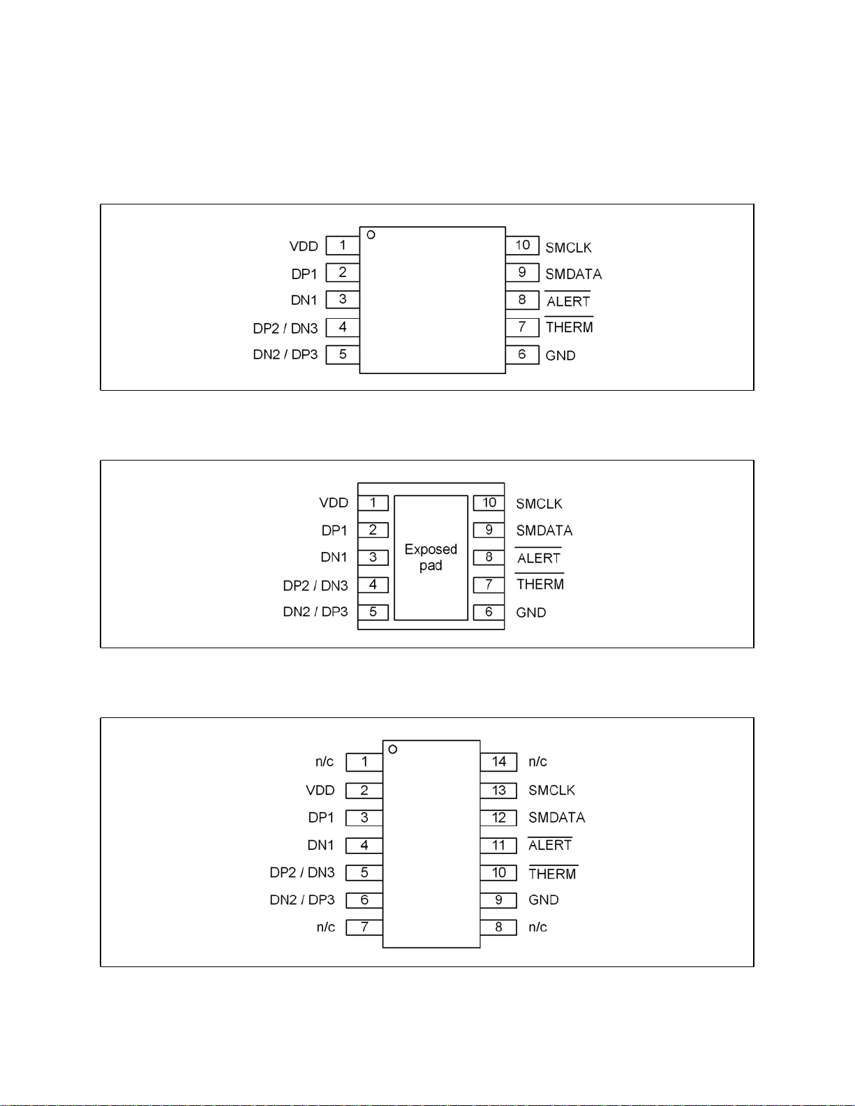
Chapter 2 Pin Description
Figure 2.1 EMC1403/EMC1404 Pin Diagram, MSOP-10
Figure 2.2 EMC1403/EMC1404 Pin Diagram, DFN-10
Figure 2.3 EMC1403/EMC1404 Pin Diagram, SOIC-14
2014 Microchip Technology Inc. DS20005272A-page 9
Page 10

Table 2.1 EMC1403 and EMC1404 Pin Description
1°C Temperature Sensor with Beta Compensation
Data Sheet
PIN
NUMBER
10-PIN
PIN
NUMBER
14-PIN NAME FUNCTION TYPE
n/a 1 n/c Not Internally Connected n/a
1 2 VDD Power supply Power
23
34
DP1 External diode 1 positive (anode)
connection
DN1 External diode 1 negative (cathode)
connection
DP2 / DN3 External diode 2 positive (anode)
45
connection / External Diode 3
negative (cathode) connection for
anti-parallel diodes
DN2 / DP3 External diode 2 negative (cathode)
56
connection / External Diode 3
positive (anode) connection for antiparallel diodes
n/a 7 n/c Not Internally Connected n/a
n/a 8 n/c Not Internally Connected n/a
6 9 GND Ground Power
710
THERM Critical THERM output signal -
requires pull-up resistor
AIO
AIO
AIO
AIO
OD (5V)
811
912
10 13
ALERT Active low digital ALERT output
SMDATA SMBus Data input/output - requires
SMCLK SMBus Clock input - requires pull-up
signal - requires pull-up resistor
pull-up resistor
resistor
OD (5V)
DIOD (5V)
DI (5V)
n/a 14 n/c Not Internally Connected n/a
DFN
Bottom
n/a
Exposed Pad Not Internally Connected,
recommend grounding.
n/a
Pad
APPLICATION NOTE: For the 5V tolerant pins that have a pull-up resistor (SMCLK, SMDATA, THERM, and
ALERT), the voltage difference between VDD and the pull-up voltage must never exceed
3.6V.
The pin types are described below:
Power - these pins are used to supply either VDD or GND to the device.
AIO - Analog Input / Output.
DI - Digital Input.
OD - Open Drain Digital Output.
DIOD - Digital Input / Open Drain Output.
DS20005272A-page 10 2014 Microchip Technology Inc.
Page 11

1°C Temperature Sensor with Beta Compensation
Data Sheet
Chapter 3 Electrical Specifications
3.1 Absolute Maximum Ratings
Table 3.1 Absolute Maximum Ratings
DESCRIPTION RATING UNIT
Supply Voltage (V
Voltage on 5V tolerant pins (V
Voltage on 5V tolerant pins (|V
Voltage on any other pin to Ground -0.3 to V
) -0.3 to 4.0 V
DD
) -0.3 to 5.5 V
5VT_pin
- VDD|) (see Note 3.1) -0.3 to 3.6 V
5VT_pin
+0.3 V
DD
Operating Temperature Range -40 to +125 °C
Storage Temperature Range -55 to +150 °C
Lead Temperature Range Refer to JEDEC Spec. J-STD-020
Package Thermal Characteristics for MSOP-10
Thermal Resistance (
) 132.2 °C/W
j-a
Package Thermal Characteristics for SOIC-14
Thermal Resistance (
) 77.7 °C/W
j-a
Package Thermal Characteristics for DFN-10
Thermal Resistance (
) 77.1 °C/W
j-a
ESD Rating, All pins HBM 2000 V
Note: Stresses at or above those listed could cause permanent damage to the device. This is a stress
rating only and functional operation of the device at any other condition above those indicated
in the operation sections of this specification is not implied. When powering this device from
laboratory or system power supplies, it is important that the Absolute Maximum Ratings not be
exceeded or device failure can result. Some power supplies exhibit voltage spikes on their
outputs when the AC power is switched on or off. In addition, voltage transients on the AC
power line may appear on the DC output. If this possibility exists, it is suggested that a clamp
circuit be used.
Note 3.1 For the 5V tolerant pins that have a pull-up resistor (SMCLK, SMDATA,
THERM, and
ALERT), the pull-up voltage must not exceed 3.6V when the device is unpowered.
2014 Microchip Technology Inc. DS20005272A-page 11
Page 12
1°C Temperature Sensor with Beta Compensation
3.2 Electrical Specifications
Table 3.2 Electrical Specifications
V
= 3.0V to 3.6V, TA = -40°C to 125°C, all typical values at TA = 27°C unless otherwise noted.
DD
CHARACTERISTIC SYMBOL MIN TYP MAX UNITS CONDITIONS
DC Power
Data Sheet
Supply Voltage V
Supply Current I
DD
DD
3.0 3.3 3.6 V
430 850 uA 1 conversion / sec, dynamic
averaging disabled
930 1200 uA 4 conversions / sec, dynamic
averaging enabled
1120 uA
> 16 conversions / sec, dynamic
averaging enabled
Standby Supply Current I
DD
170 230 uA Device in Standby mode, no SMBus
communications, ALERT and
THERM pins not asserted.
Internal Temperature Monitor
Temperature Accuracy ±0.25 ±1 °C -5°C < T
±2 °C -40°C < T
Temperature Resolution 0.125 °C
External Temperature Monitor
Temperature Accuracy ±0.25 ±1 °C +20°C < T
0°C < TA < 100°C
±0.5 ±2 °C -40°C < T
Temperature Resolution 0.125 °C
< 100°C
A
< 125°C
A
DIODE
DIODE
< +110°C
< 127°C
Capacitive Filter C
t
CONV
t
CONV
FILTER
190 ms EMC1403, default settings
150 ms EMC1404, default settings
2.2 2.5 nF Connected across external diode
ALERT and THERM pins
Output Low Voltage V
Leakage Current I
OL
LEAK
0.4 V I
±5 uA ALERT and THERM pins
= 8mA
SINK
Device powered or unpowered
TA < 85°C
pull-up voltage < 3.6V
DS20005272A-page 12 2014 Microchip Technology Inc.
Page 13

1°C Temperature Sensor with Beta Compensation
Data Sheet
3.3 SMBus Electrical Characteristics
Table 3.3 SMBus Electrical Specifications
V
= 3.0V to 3.6V, TA = -40°C to 125°C, all typical values are at TA = 27°C unless otherwise noted.
DD
CHARACTERISTIC SYMBOL MIN TYP MAX UNITS CONDITIONS
SMBus Interface
Input High Voltage V
Input Low Voltage V
Input High/Low Current I
IH
IL
IH / IIL
2.0 V
V 5V Tolerant
DD
-0.3 0.8 V 5V Tolerant
±5 uA Powered or unpowered
Hysteresis 420 mV
Input Capacitance C
Output Low Sink Current I
OL
IN
8.2 15 mA SMDATA = 0.4V
5pF
SMBus Timing
Clock Frequency f
Spike Suppression t
Bus free time Start to
Stop
Hold Time: Start t
Setup Time: Start t
Setup Time: Stop t
Data Hold Time t
Data Hold Time t
Data Setup Time t
Clock Low Period t
Clock High Period t
Clock/Data Fall time t
Clock/Data Rise time t
Capacitive Load C
SMB
SP
t
BUF
HD:STA
SU:STA
SU:STP
HD:DAT
HD:DAT
SU:DAT
LOW
HIGH
FALL
RISE
LOAD
10 400 kHz
50 ns
1.3 us
0.6 us
0.6 us
0.6 us
0 us When transmitting to the master
0.3 us When receiving from the master
100 ns
1.3 us
0.6 us
300 ns Min = 20+0.1C
300 ns Min = 20+0.1C
400 pF per bus line
TA < 85°C
LOAD
LOAD
ns
ns
2014 Microchip Technology Inc. DS20005272A-page 13
Page 14
1°C Temperature Sensor with Beta Compensation
Data Sheet
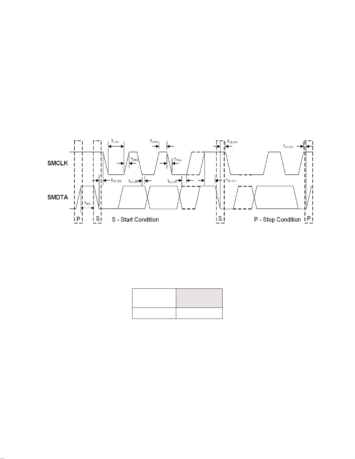
Chapter 4 System Management Bus Interface Protocol
4.1 System Management Bus Interface Protocol
The EMC1403 and EMC1404 communicate with a host controller, such as an SIO, through the SMBus.
The SMBus is a two-wire serial communication protocol between a computer host and its peripheral
devices. A detailed timing diagram is shown in
For the first 15ms after power-up the device may not respond to SMBus communications.
.
Figure 4.1.
Figure 4.1 SMBus Timing Diagram
The EMC1403 and EMC1404 are SMBus 2.0 compatible and support Send Byte, Read Byte, Write
Byte, Receive Byte, and the Alert Response Address as valid protocols as shown below.
All of the below protocols use the convention in Table 4.1.
Table 4.1 Protocol Format
DATA SENT
TO DEVICE
# of bits sent # of bits sent
Attempting to communicate with the EMC1403 and EMC1404 SMBus interface with an invalid slave
address or invalid protocol will result in no response from the device and will not affect its register
contents. Stretching of the SMCLK signal is supported, provided other devices on the SMBus control
the timing.
DATA SENT TO
THE HOST
DS20005272A-page 14 2014 Microchip Technology Inc.
Page 15

1°C Temperature Sensor with Beta Compensation
Data Sheet
4.2 Write Byte
The Write Byte is used to write one byte of data to the registers as shown below Table 4.2:
Table 4.2 Write Byte Protocol
START
SLAVE
ADDRESS WR
ACK
REGISTER
ADDRESS ACK
REGISTER
DATA ACK STOP
1 -> 0 1001_100 0 0 XXh 0 XXh 0 0 -> 1
4.3 Read Byte
The Read Byte protocol is used to read one byte of data from the registers as shown in Table 4.3.
Table 4.3 Read Byte Protocol
START SLAVE
ADDRESS
WR ACK REGISTER
ADDRESS
ACK START SLAVE
ADDRESS
RD ACK REGISTER
DATA
NACK STOP
1 -> 0 1001_100 0 1 XXh 0 1 -> 0 1001_100 1 1 XX 1 0 -> 1
4.4 Send Byte
The Send Byte protocol is used to set the internal address register pointer to the correct address
START
location. No data is transferred during the Send Byte protocol as shown in
Table 4.4 Send Byte Protocol
SLAVE
ADDRESS WR
ACK
REGISTER
ADDRESS ACK STOP
Table 4.4.
1 -> 0 1001_100 0 0 XXh 0 0 -> 1
4.5 Receive Byte
The Receive Byte protocol is used to read data from a register when the internal register address
pointer is known to be at the right location (e.g. set via Send Byte). This is used for consecutive reads
of the same register as shown in
SLAVE
START
ADDRESS RD
1 -> 0 1001_100 1 0 XXh 1 0 -> 1
2014 Microchip Technology Inc. DS20005272A-page 15
Table 4.5.
Table 4.5 Receive Byte Protocol
ACK REGISTER DATA NACK STOP
Page 16

4.6 Alert Response Address
The ALERT output can be used as a processor interrupt or as an SMBus Alert.
When it detects that the ALERT pin is asserted, the host will send the Alert Response Address (ARA)
to the general address of 0001_100xb. All devices with active interrupts will respond with their client
address as shown in
Table 4.6.
Table 4.6 Alert Response Address Protocol
1°C Temperature Sensor with Beta Compensation
Data Sheet
ALERT
START
1 -> 0 0001_100 1 0 1001_1000 1 0 -> 1
APPLICATION NOTE: The ARA does not clear the Status Register and if the MASK bit is cleared prior to the Status
RESPONSE
ADDRESS RD
The EMC1403 and EMC1404 will respond to the ARA in the following way:
1. Send Slave Address and verify that full slave address was sent (i.e. the SMBus communication
from the device was not prematurely stopped due to a bus contention event).
2. Set the MASK bit to clear the ALERT pin.
Register being cleared, the
ACK
ALERT pin will be reasserted.
DEVICE
ADDRESS NACK STOP
4.7 SMBus Address
The EMC1403 and EMC1404 respond to hard-wired SMBus slave address as shown in Table 1.1.
Note: Other addresses are available. Contact Microchip for more information.
4.8 SMBus Timeout
The EMC1403 and EMC1404 support SMBus Timeout. If the clock line is held low for longer than
30ms, the device will reset its SMBus protocol. This function can be enabled by setting the TIMEOUT
bit in the Consecutive Alert Register (see
Section 6.12).
DS20005272A-page 16 2014 Microchip Technology Inc.
Page 17
1°C Temperature Sensor with Beta Compensation
Data Sheet
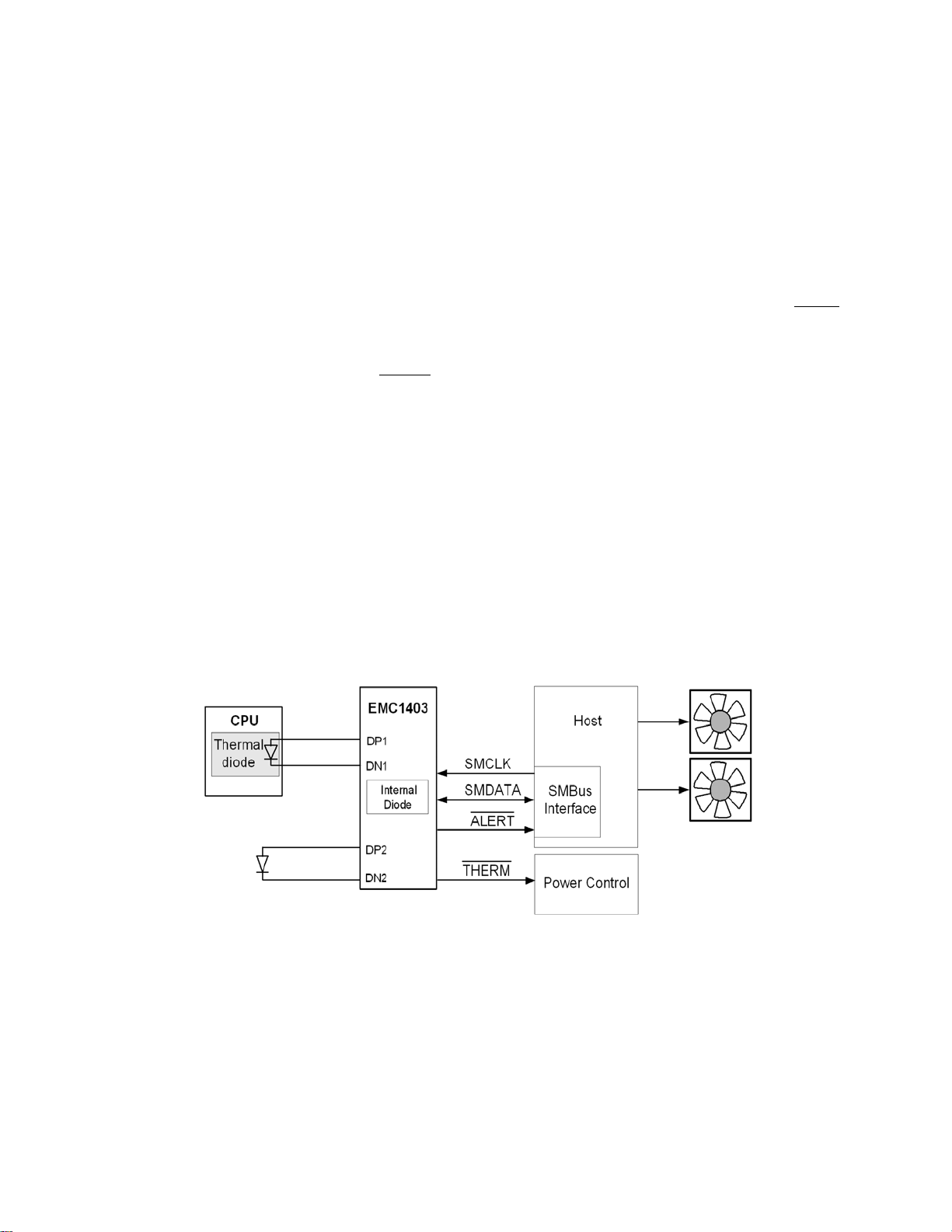
Chapter 5 Product Description
The EMC1403 and EMC1404 are SMBus temperature sensors. The EMC1403 monitors one internal
diode and two externally connected temperature diodes. The EMC1404 monitors one internal diode
and three externally connected temperature diodes.
Thermal management is performed in cooperation with a host device. This consists of the host reading
the temperature data of both the external and internal temperature diodes of the EMC1403 and
EMC1404 and using that data to control the speed of one or more fans.
The EMC1403 and EMC1404 have two levels of monitoring. The first provides a maskable ALERT
signal to the host when the measured temperatures exceeds user programmable limits. This allows
the EMC1403 or EMC1404 to be used as an independent thermal watchdog to warn the host of
temperature hot spots without direct control by the host. The second level of monitoring provides a non
maskable interrupt on the
programmable limit.
Since the EMC1403 and EMC1404 automatically correct for temperature errors due to series
resistance in temperature diode lines, there is greater flexibility in where external diodes are positioned
and better measurement accuracy than previously available with non-resistance error correcting
devices. The automatic beta detection feature means that there is no need to program the device
according to which type of diode is present on the External Diode 1 channel. This also includes CPU
diodes that require the transistor or BJT model for monitoring their temperature. Therefore, the
EMC1403/EMC1404 can power up ready to operate for any system configuration.
For the EMC1404, External Diode channels 2 and 3 are only compatible with general purpose diodes
(such as a 2N3904).
Figure 5.1 shows a system level block diagram of the EMC1403. Figure 5.2 shows a system level block
diagram of the EMC1404.
THERM pin if the measured temperatures meet or exceed a second
Figure 5.1 System Diagram for EMC1403
2014 Microchip Technology Inc. DS20005272A-page 17
Page 18

Figure 5.2 System Diagram for EMC1404
5.1 Modes of Operation
1°C Temperature Sensor with Beta Compensation
Data Sheet
The EMC1403 and EMC1404 have two modes of operation.
Active (Run) - In this mode of operation, the ADC is converting on all temperature channels at the
programmed conversion rate. The temperature data is updated at the end of every conversion and
the limits are checked. In Active mode, writing to the one-shot register will do nothing.
Standby (Stop) - In this mode of operation, the majority of circuitry is powered down to reduce
supply current. The temperature data is not updated and the limits are not checked. In this mode
of operation, the SMBus is fully active and the part will return requested data. Writing to the oneshot register will enable the device to update all temperature channels. Once all the channels are
updated, the device will return to the Standby mode.
5.1.1 Conversion Rates
The EMC1403 and EMC1404 may be configured for different conversion rates based on the system
requirements. The conversion rate is configured as described in
rate is 4 conversions per second. Other available conversion rates are shown in Table 6.6.
5.1.2 Dynamic Averaging
Dynamic averaging causes the EMC1403 and EMC1404 to measure the external diode channels for
an extended time based on the selected conversion rate. This functionality can be disabled for
increased power savings at the lower conversion rates (see
enabled, the device will automatically adjust the sampling and measurement time for the external diode
channels. This allows the device to average 2x or 16x longer than the normal 11 bit operation
(nominally 21ms per channel) while still maintaining the selected conversion rate. The benefits of
dynamic averaging are improved noise rejection due to the longer integration time as well as less
random variation of the temperature measurement.
When enabled, the dynamic averaging applies when a one-shot command is issued. The device will
perform the desired averaging during the one-shot operation according to the selected conversion rate.
When enabled, the dynamic averaging will affect the average supply current based on the chosen
conversion rate as shown in
Section 6.5. The default conversion
Section 6.4). When dynamic averaging is
Table 5.1 for EMC1403.
DS20005272A-page 18 2014 Microchip Technology Inc.
Page 19

1°C Temperature Sensor with Beta Compensation
Data Sheet
Table 5.1 Supply Current vs. Conversion Rate for EMC1403
CONVERSION RATE
1 / 16 sec 660uA 430uA 16x 1x
1 / 8 sec 660uA 430uA 16x 1x
1 / 4 sec 660uA 430uA 16x 1x
1 / 2 sec 660uA 430uA 16x 1x
1 / sec 660uA 430uA 16x 1x
2 / sec 930uA 475uA 8x 1x
4 / sec (default) 950uA 510uA 4x 1x
8 / sec 1010uA 630uA 2x 1x
16 / sec 1020uA 775uA 1x 1x
32 / sec 1050uA 1050uA 0.5x 0.5x
64 / sec 1100uA 1100uA 0.25x 0.25x
When enabled, the dynamic averaging will affect the average supply current based on the chosen
conversion rate as shown in
AVERAGE SUPPLY CURRENT
ENABLED
(DEFAULT) DISABLED
Table 5.2 for EMC1404.
AVERAGING FACTOR (BASED ON
11-BIT OPERATION)
ENABLED
(DEFAULT) DISABLED
Table 5.2 Supply Current vs. Conversion Rate for EMC1404
AVERAGING FACTOR (BASED ON 1 1-BIT
CONVERSION RATE
AVERAGE SUPPLY CURRENT
ENABLED
(DEFAULT) DISABLED
ENABLED
(DEFAULT) DISABLED
OPERATION)
1 / 16 sec 660uA 430uA 16x 1x
1 / 8 sec 660uA 430uA 16x 1x
1 / 4 sec 660uA 430uA 16x 1x
1 / 2 sec 660uA 430uA 16x 1x
1 / sec 660uA 430uA 8x 1x
2 / sec 930uA 475uA 4x 1x
4 / sec (default) 950uA 510uA 2x 1x
8 / sec 1010uA 630uA 1x 1x
16 / sec 1020uA 775uA 0.5x 0.5x
2014 Microchip Technology Inc. DS20005272A-page 19
Page 20

1°C Temperature Sensor with Beta Compensation
Table 5.2 Supply Current vs. Conversion Rate for EMC1404 (continued)
Data Sheet
AVERAGE SUPPLY CURRENT
CONVERSION RATE
32 / sec 1050uA 1050uA 0.25x 0.25x
64 / sec 1100uA 1100uA 0.125x 0.125x
ENABLED
(DEFAULT) DISABLED
5.2 THERM Output
The THERM output is asserted independently of the ALERT output and cannot be masked. Whenever
any of the measured temperatures exceed the user programmed THERM Limit values for the
programmed number of consecutive measurements, the
asserted, it will remain asserted until all measured temperatures drop below the THERM Limit minus
the THERM Hysteresis (also programmable).
When the THERM pin is asserted, the Therm status bits will likewise be set. Reading these bits will
not clear them until the
status bits will be automatically cleared.
5.3 ALERT Output
The ALERT pin is an open drain output and requires a pull-up resistor to VDD and has two modes of
operation: interrupt mode and comparator Mode. The mode of the
ALERT / COMP bit in the Configuration Register (see
AVERAGING FACTOR (BASED ON 1 1-BIT
OPERATION)
ENABLED
(DEFAULT) DISABLED
THERM output is asserted. Once it has been
THERM pin is deasserted. Once the THERM pin is deasserted, the THERM
ALERT output is selected via the
Section 6.4).
5.3.1 ALERT Pin Interrupt Mode
When configured to operate in interrupt mode, the ALERT pin asserts low when an out of limit
measurement (
The
ALERT pin will remain asserted as long as an out-of-limit condition remains. Once the out-of-limit
condition has been removed, the
cleared.
The ALERT pin can be masked by setting the MASK bit. Once the ALERT pin has been masked, it
will be de-asserted and remain de-asserted until the MASK bit is cleared by the user. Any interrupt
conditions that occur while the
The ALERT pin is used as an interrupt signal or as an Smbus Alert signal that allows an SMBus slave
to communicate an error condition to the master. One or more
together.
> high limit or < low limit) is detected on any diode or when a diode fault is detected.
ALERT pin will remain asserted until the appropriate status bits are
ALERT pin is masked will update the Status Register normally.
5.3.2 ALERT Pin Comparator Mode
When the ALERT pin is configured to operate in comparator mode it will be asserted if any of the
measured temperatures exceeds the respective high limit. The
all temperatures drop below the corresponding high limit minus the THERM Hysteresis value.
When the ALERT pin is asserted in comparator mode, the corresponding high limit status bits will be
set. Reading these bits will not clear them until the
deasserted, the status bits will be automatically cleared.
The MASK bit will not block the ALERT pin in this mode, however the individual channel masks (see
Section 6.11) will prevent the respective channel from asserting the ALERT pin.
ALERT outputs can be hard-wired
ALERT pin will remain asserted until
ALERT pin is deasserted. Once the ALERT pin is
DS20005272A-page 20 2014 Microchip Technology Inc.
Page 21

1°C Temperature Sensor with Beta Compensation
Data Sheet
5.4 Beta Compensation
The EMC1403 and EMC1404 are configured to monitor the temperature of basic diodes (e.g. 2N3904),
or CPU thermal diodes. It automatically detects the type of external diode (CPU diode or diode
connected transistor) and determines the optimal setting to reduce temperature errors introduced by
beta variation for the External Diode 1 channel only. Compensating for this error is also known as
implementing the transistor or BJT model for temperature measurement.
For discrete transistors configured with the collector and base shorted together, the beta is generally
sufficiently high such that the percent change in beta variation is very small. For example, a 10%
variation in beta for two forced emitter currents with a transistor whose ideal beta is 50 would contribute
approximately 0.25°C error at 100°C. However for substrate transistors where the base-emitter junction
is used for temperature measurement and the collector is tied to the substrate, the proportional beta
variation will cause large error. For example, a 10% variation in beta for two forced emitter currents
with a transistor whose ideal beta is 0.5 would contribute approximately 8.25°C error at 100°C.
The External Diode 2 and External Diode 3 channels do not support Beta Compensation.
5.5 Resistance Error Correction (REC)
Parasitic resistance in series with the external diodes will limit the accuracy obtainable from
temperature measurement devices. The voltage developed across this resistance by the switching
diode currents cause the temperature measurement to read higher than the true temperature.
Contributors to series resistance are PCB trace resistance, on die (i.e. on the processor) metal
resistance, bulk resistance in the base and emitter of the temperature transistor. Typically, the error
caused by series resistance is +0.7°C per ohm. The EMC1403 and EMC1404 automatically correct up
to 100 ohms of series resistance.
5.6 Programmable External Diode Ideality Factor
The EMC1403 and EMC1404 is designed for external diodes with an ideality factor of 1.008. Not all
external diodes, processor or discrete, will have this exact value. This variation of the ideality factor
introduces error in the temperature measurement which must be corrected for. This correction is
typically done using programmable offset registers. Since an ideality factor mismatch introduces an
error that is a function of temperature, this correction is only accurate within a small range of
temperatures. To provide maximum flexibility to the user, the EMC1403 and EMC1404 provides a 6bit register for each external diode where the ideality factor of the diode used is programmed to
eliminate errors across all temperatures.
APPLICATION NOTE: When monitoring a substrate transistor or CPU diode and beta compensation is enabled, the
Ideality Factor should not be adjusted. Beta Compensation automatically corrects for most
ideality errors.
5.7 Diode Faults
The EMC1403 and EMC1404 detect an open on the DP and DN pins, and a short across the DP and
DN pins. For each temperature measurement made, the device checks for a diode fault on the external
diode channel(s). When a diode fault is detected, the ALERT pin asserts (unless masked, see
Section 5.8) and the temperature data reads 00h in the MSB and LSB registers (note: the low limit will
not be checked). A diode fault is defined as one of the following: an open between DP and DN, a short
from V
If a short occurs across DP and DN or a short occurs from DP to GND, the low limit status bit is set
and the ALERT pin asserts (unless masked). This condition is indistinguishable from a temperature
measurement of 0.000degC (-64°C in extended range) resulting in temperature data of 00h in the MSB
and LSB registers.
If a short from DN to GND occurs (with a diode connected), temperature measurements will continue
as normal with no alerts.
to DP, or a short from VDD to DN.
DD
2014 Microchip Technology Inc. DS20005272A-page 21
Page 22
5.8 Consecutive Alerts
The EMC1403 and EMC1404 contain multiple consecutive alert counters. One set of counters applies
to the
ALERT pin and the second set of counters applies to the THERM pin. Each temperature
measurement channel has a separate consecutive alert counter for each of the
pins. All counters are user programmable and determine the number of consecutive measurements
that a temperature channel(s) must be out-of-limit or reporting a diode fault before the corresponding
pin is asserted.
See Section 6.12 for more details on the consecutive alert function.
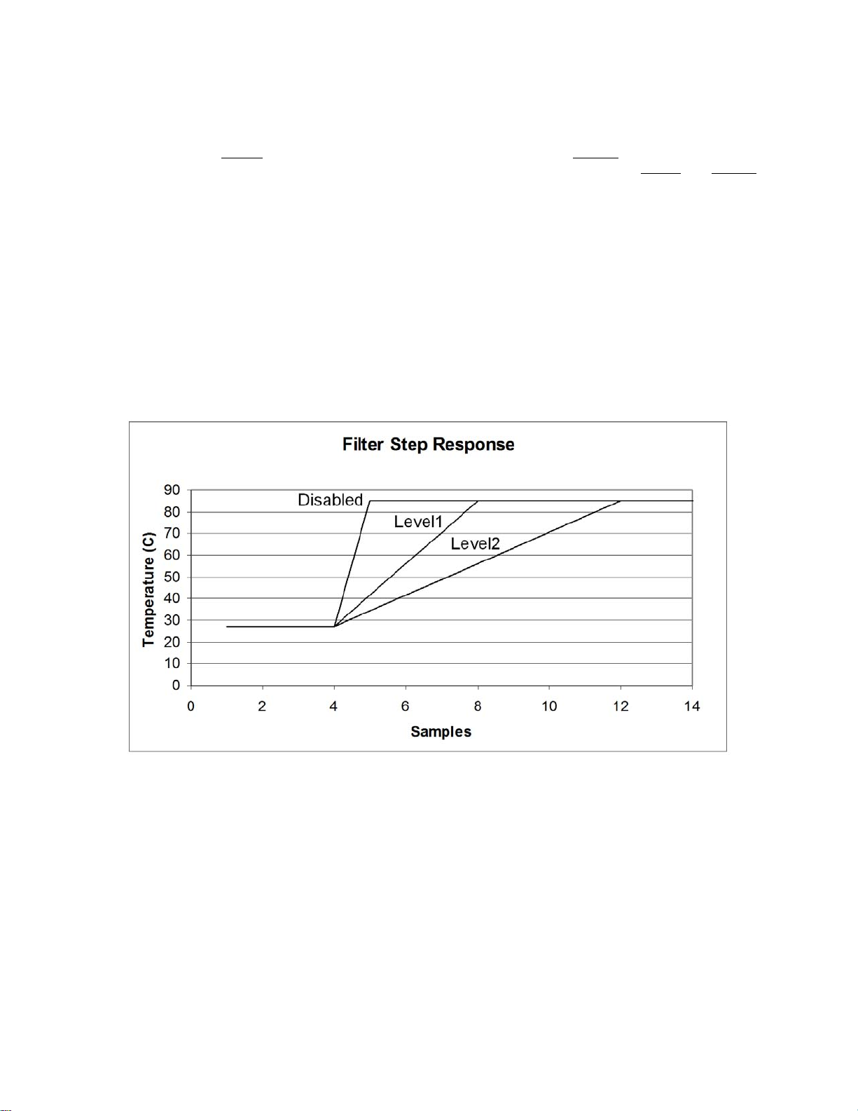
5.9 Digital Filter
To reduce the effect of noise and temperature spikes on the reported temperature, the External Diode
1 channel uses a programmable digital filter. This filter can be configured as Level 1, Level 2, or
Disabled. The typical filter performance is shown in
1°C Temperature Sensor with Beta Compensation
Data Sheet
ALERT and THERM
Figure 5.3 and Figure 5.4.
Figure 5.3 Temperature Filter Step Response
DS20005272A-page 22 2014 Microchip Technology Inc.
Page 23
1°C Temperature Sensor with Beta Compensation
Data Sheet
Figure 5.4 Temperature Filter Impulse Response
5.10 Temperature Monitors
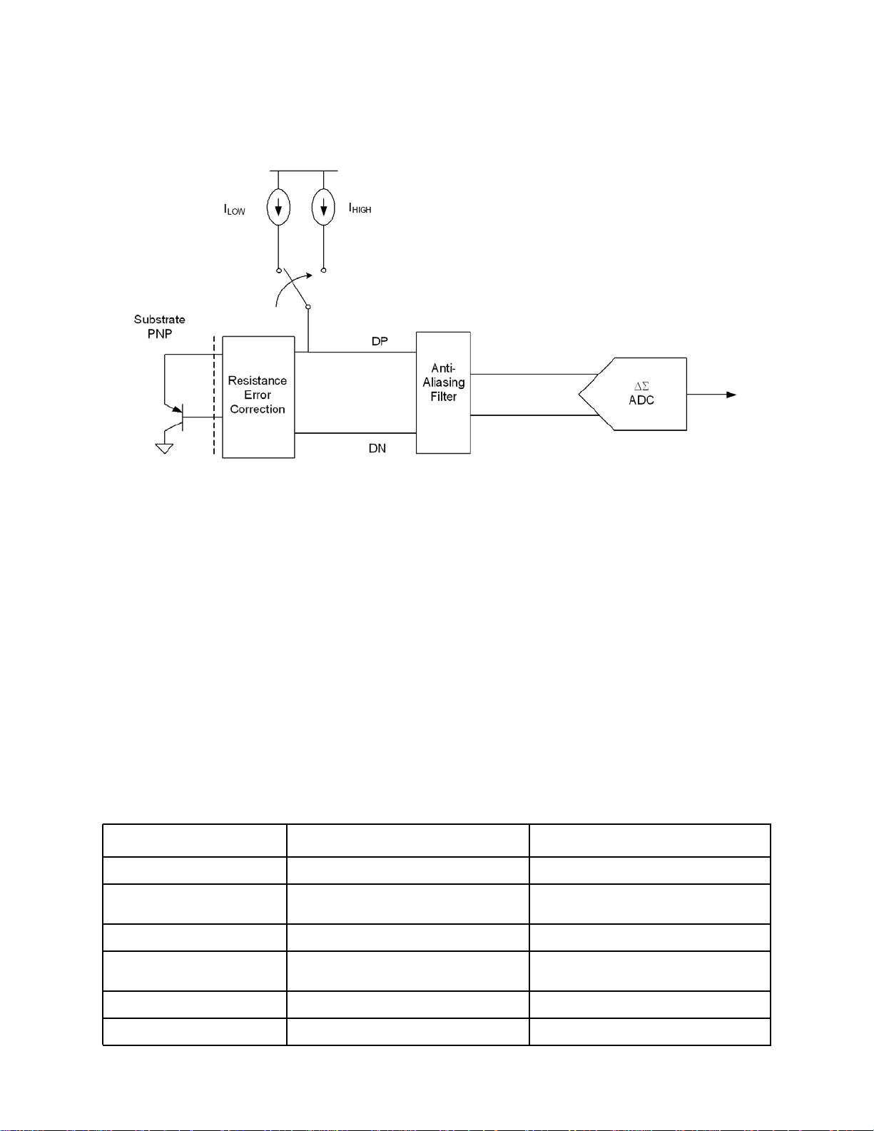
In general, thermal diode temperature measurements are based on the change in forward bias voltage
of a diode when operated at two different currents. This
as shown in the following equation:
Figure 5.5 shows a block diagram of the temperature measurement circuit. The negative terminal for
the remote temperature diode, DN, is internally biased with a forward diode voltage referenced to
ground.
VBE is proportional to absolute temperature
where:
k = Boltzmann’s constant
T = absolute temperature in Kelvin [1]
q = electron charge
= diode ideality factor
2014 Microchip Technology Inc. DS20005272A-page 23
Page 24
1°C Temperature Sensor with Beta Compensation
Data Sheet
Figure 5.5 Block Diagram of Temperature Monitoring Circuit
5.11 Temperature Measurement Results and Data
The temperature measurement results are stored in the internal and external temperature registers.
These are then compared with the values stored in the high and low limit registers. Both external and
internal temperature measurements are stored in 11-bit format with the eight (8) most significant bits
stored in a high byte register and the three (3) least significant bits stored in the three (3) MSB
positions of the low byte register. All other bits of the low byte register are set to zero.
The EMC1403 and EMC1404 have two selectable temperature ranges. The default range is from 0°C
to +127°C and the temperature is represented as binary number able to report a temperature from 0°C
to +127.875°C in 0.125°C steps.
The extended range is an extended temperature range from -64°C to +191°C. The data format is a
binary number offset by 64°C. The extended range is used to measure temperature diodes with a large
known offset (such as AMD processor diodes) where the diode temperature plus the offset would be
equivalent to a temperature higher than +127°C.
Table 5.3 shows the default and extended range formats.
Table 5.3 Temperature Data Format
TEMPERATURE (°C) DEFAULT RANGE 0°C TO 127°C EXTENDED RANGE -64°C TO 191°C
Diode Fault 000 0000 0000 000 0000 0000
-64 000 0000 0000 000 0000 0000
Note 5.2
-1 000 0000 0000 001 1111 1000
0 000 0000 0000
Note 5.1
0.125 000 0000 0001 010 0000 0001
1 000 0000 1000 010 0000 1000
DS20005272A-page 24 2014 Microchip Technology Inc.
010 0000 0000
Page 25

1°C Temperature Sensor with Beta Compensation
Data Sheet
Table 5.3 Temperature Data Format (continued)
TEMPERATURE (°C) DEFAULT RANGE 0°C TO 127°C EXTENDED RANGE -64°C TO 191°C
64 010 0000 0000 100 0000 0000
65 010 0000 1000 100 0000 1000
127 011 1111 1000 101 1111 1000
127.875 011 1111 1111 101 1111 1111
128 011 1111 1111
Note 5.3
190 011 1111 1111 111 1111 0000
191 011 1111 1111 111 1111 1000
>= 191.875 011 1111 1111 111 1111 1111
Note 5.1 In default mode, all temperatures < 0°C will be reported as 0°C.
Note 5.2 In the extended range, all temperatures < -64°C will be reported as -64°C.
Note 5.3 For the default range, all temperatures > +127.875°C will be reported as +127.875°C.
Note 5.4 For the extended range, all temperatures > +191.875°C will be reported as +191.875°C.
110 0000 0000
Note 5.4
5.12 Anti-parallel Diode Connections
The EMC1404 supports reading two external diodes on the same set of pins (DP2, DN2). These
diodes are connected as shown in
diodes will be reverse biased by a VBE voltage (approximately 0.7V). Because of this reverse bias,
only discrete thermal diodes (such as a 2N3904) are recommended to be placed on these pins.
Figure 5.2. Due to the anti-parallel connection of these diodes, both
5.13 External Diode Connections
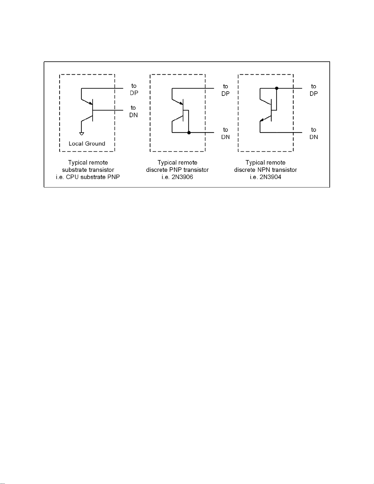
The EMC1403 can be configured to measure a CPU substrate transistor, a discrete 2N3904 thermal
diode, or an AMD processor diode. The diodes can be connected in a variety of ways as indicated in
Figure 5.6.
The EMC1404 can be configured to measure a CPU substrate transistor, a discrete 2N3904 thermal
diode, or an AMD processor diode on the External Diode 1 channel only. The External Diode 2 and
External Diode 3 channels are configured to measure a pair of discrete anti-parallel diodes (shared on
pins DP2 and DN2). The supported configurations for the external diode channels are shown in
Figure 5.6.
2014 Microchip Technology Inc. DS20005272A-page 25
Page 26
1°C Temperature Sensor with Beta Compensation
Figure 5.6 Diode Configurations
Data Sheet
DS20005272A-page 26 2014 Microchip Technology Inc.
Page 27

1°C Temperature Sensor with Beta Compensation
Data Sheet
Chapter 6 Register Description
The registers shown in Table 6.1 are accessible through the SMBus. An entry of ‘-’ indicates that the
bit is not used and will always read ‘0’.
Table 6.1 Register Set in Hexadecimal Order
REGISTER
ADDRESS R/W REGISTER NAME FUNCTION
00h R
01h R
02h R Status
03h R/W Configuration
04h R/W Conversion Rate
05h R/W
06h R/W
07h R/W
Internal Diode Data
High Byte
External Diode 1
Data High Byte
Internal Diode High
Limit
Internal Diode Low
Limit
External Diode 1
High Limit High Byte
Stores the integer data for the
Internal Diode
Stores the integer data for External
Diode 1
Stores the status bits for the
Internal Diode and External Diodes
Controls the general operation of
the device (mirrored at address
09h)
Controls the conversion rate for
updating temperature data
(mirrored at address 0Ah)
Stores the 8-bit high limit for the
Internal Diode (mirrored at address
0Bh)
Stores the 8-bit low limit for the
Internal Diode (mirrored at address
0Ch)
Stores the integer portion of the
high limit for External Diode 1
(mirrored at register 0Dh)
DEFAULT
VALUE PAGE
00h
Page 30
00h
00h Page 31
00h Page 31
06h
(4/sec)
55h
(85°C)
00h
(0°C)
55h
(85°C)
Page 32
Page 33
08h R/W
09h R/W Configuration
0Ah R/W Conversion Rate
2014 Microchip Technology Inc. DS20005272A-page 27
External Diode 1 Low
Limit High Byte
Stores the integer portion of the
low limit for External Diode 1
(mirrored at register 0Eh)
Controls the general operation of
the device (mirrored at address
03h)
Controls the conversion rate for
updating temperature data
(mirrored at address 04h)
00h
(0°C)
00h Page 31
06h
(4/sec)
Page 32
Page 28

1°C Temperature Sensor with Beta Compensation
Table 6.1 Register Set in Hexadecimal Order (continued)
Data Sheet
REGISTER
ADDRESS R/W REGISTER NAME FUNCTION
0Bh R/W
0Ch R/W
0Dh R/W
0Eh R/W
Internal Diode High
Limit
Internal Diode Low
Limit
External Diode 1
High Limit High Byte
External Diode 1 Low
Limit High Byte
0Fh W One shot
10h R
External Diode 1
Data Low Byte
11h R/W Scratchpad
12h R/W Scratchpad
Stores the 8-bit high limit for the
Internal Diode (mirrored at address
05h)
Stores the 8-bit low limit for the
Internal Diode (mirrored at address
06h)
Stores the integer portion of the
high limit for External Diode 1
(mirrored at register 07h)
Stores the integer portion of the
low limit for External Diode 1
(mirrored at register 08h)
A write to this register initiates a
one shot update.
Stores the fractional data for
External Diode 1
Scratchpad register for software
compatibility
Scratchpad register for software
compatibility
DEFAULT
VALUE PAGE
55h
(85°C)
00h
(0°C)
Page 33
55h
(85°C)
00h
(0°C)
00h Page 35
00h Page 30
00h Page 35
00h Page 35
13h R/W
14h R/W
15h R/W
16h R/W
17h R/W
18h R/W
19h R/W
1Ah R/W
External Diode 1
High Limit Low Byte
External Diode 1 Low
Limit Low Byte
External Diode 2
High Limit High Byte
External DIode 2 Low
Limit High Byte
External Diode 2
High Limit Low Byte
External Diode 2 Low
Limit Low Byte
External Diode 1
THERM Limit
External Diode 2
THERM Limit
1Bh R-C External Diode Fault
1Fh R/W
Channel Mask
Register
Stores the fractional portion of the
high limit for External Diode 1
Stores the fractional portion of the
low limit for External Diode 1
Stores the integer portion of the
high limit for External Diode 2
Stores the integer portion of the
low limit for External Diode 2
Stores the fractional portion of the
high limit External Diode 2
Stores the fractional portion of the
low limit for External Diode 2
Stores the 8-bit critical temperature
limit for External Diode 1
Stores the 8-bit critical temperature
limit for External Diode 2
Stores status bits indicating which
external diode detected a diode
fault
Controls the masking of individual
channels
00h
Page 33
00h
55h
(85°C)
Page 33
00h
(0°C)
00h
Page 33
00h
55h
(85°C)
55h
(85°C)
Page 35
Page 35
00h Page 36
00h Page 36
DS20005272A-page 28 2014 Microchip Technology Inc.
Page 29

1°C Temperature Sensor with Beta Compensation
Data Sheet
Table 6.1 Register Set in Hexadecimal Order (continued)
REGISTER
ADDRESS R/W REGISTER NAME FUNCTION
20h R/W
Internal Diode
THERM Limit
21h R/W THERM Hysteresis
Stores the 8-bit critical temperature
limit for the Internal Diode
Stores the 8-bit hysteresis value
that applies to all THERM limits
Controls the number of out-of-limit
22h R/W Consecutive ALERT
conditions that must occur before
an interrupt is asserted
23h R
24h R
25h R/W
26h R/W
27h R/W
External Diode 2
Data High Byte
External Diode 2
Data Low Byte
External Diode 1
Beta Configuration
External Diode 2
Beta Configuration
External Diode 1
Ideality Factor
Stores the integer data for External
Diode 2
Stores the fractional data for
External Diode 2
Stores the Beta Compensation
circuitry settings for External Diode
1
Stores the Beta Compensation
circuitry settings for External Diode 208h or 07h Page 38
Stores the ideality factor for
External Diode 1
DEFAULT
VALUE PAGE
55h
(85°C)
Page 35
0Ah
(10°C)
70h Page 37
00h
Page 30
00h
08h Page 38
12h
(1.008)
Page 39
28h R/W
29h R
2Ah R
2Bh R
2Ch R/W
2Dh R/W
2Eh R/W
2Fh R/W
30h R/W
31h R/W
External Diode 2
Ideality Factor
Internal Diode Data
Low Byte
External Diode 3
High Byte
External Diode 3 Low
Byte
External Diode 3
High Limit High Byte
External Diode 3 Low
Limit High Byte
External Diode 3
High Limit Low Byte
External Diode 3 Low
Limit Low Byte
External Diode 3
THERM Limit
External Diode 3
Ideality Factor
Stores the ideality factor for
External Diode 2
Stores the fractional data for the
Internal Diode
Stores the integer data for External
Diode 3
Stores the fractional data for
External Diode 3
Stores the integer portion of the
high limit for External Diode 3
Stores the integer portion of the
low limit for External Diode 3
Stores the fractional portion of the
high limit for External Diode 3
Stores the fractional portion of the
low limit for External Diode 3
Stores the 8-bit critical temperature
limit for External Diode 3
Stores the ideality factor for
External Diode 3
12h
(1.008)
Page 39
00h Page 30
00h
Page 30
00h
55h
(85°C)
00h
(0°C)
Page 33
00h
00h
55h
(85°C)
12h
(1.008)
Page 35
Page 39
35h R-C High Limit Status Status bits for the High Limits 00h Page 41
36h R-C Low Limit Status Status bits for the Low Limits 00h Page 41
2014 Microchip Technology Inc. DS20005272A-page 29
Page 30

1°C Temperature Sensor with Beta Compensation
Table 6.1 Register Set in Hexadecimal Order (continued)
Data Sheet
REGISTER
ADDRESS R/W REGISTER NAME FUNCTION
37h R THERM Limit Status Status bits for the THERM Limits 00h Page 42
40h R/W Filter Control
FDh R Product ID
FEh R Microchip ID
FFh R Revision
Controls the digital filter setting for
the External Diode 1 channel
Stores a fixed value that identifies
each product
Stores a fixed value that
represents Microchip
Stores a fixed value that
represents the revision number
DEFAULT
VALUE PAGE
00h Page 42
Table 6.25 Page 43
5Dh Page 43
01h or 04h Page 44
6.1 Data Read Interlock
When any temperature channel high byte register is read, the corresponding low byte is copied into
an internal ‘shadow’ register. The user is free to read the low byte at any time and be guaranteed that
it will correspond to the previously read high byte. Regardless if the low byte is read or not, reading
from the same high byte register again will automatically refresh this stored low byte data.
6.2 Temperature Data Registers
Table 6.2 Temperature Data Registers
ADDR R/W REGISTER B7 B6 B5 B4 B3 B2 B1 B0 DEFAULT
00h R
29h R
01h R
10h R
23h R
24h R
2Ah R
2Bh R
As shown in Table 6.2, all temperatures are stored as an 11-bit value with the high byte representing
the integer value and the low byte representing the fractional value left justified to occupy the MSBits.
Internal Diode
High Byte
Internal Diode
Low Byte
External Diode
1 High Byte
External Diode
1 Low Byte
External Diode
2 High Byte
External Diode
2 Low Byte
External Diode
3 High Byte
External Diode
3 Low Byte
128 64 32 16 8 4 2 1 00h
0.5 0.25 0.125 - - - - - 00h
128 64 32 16 8 4 2 1 00h
0.5 0.25 0.125 - - - - - 00h
128 64 32 16 8 4 2 1 00h
0.5 0.25 0.125 - - - - - 00h
128 64 32 16 8 4 2 1 00h
0.5 0.25 0.125 - - - - - 00h
DS20005272A-page 30 2014 Microchip Technology Inc.
Page 31

1°C Temperature Sensor with Beta Compensation
Data Sheet
6.3 Status Register
Table 6.3 Status Register
ADDR R/W REGISTER B7 B6 B5 B4 B3 B2 B1 B0 DEFAULT
02h R Status BUSY - - HIGH LOW FAULT THERM - 00h
The Status Register reports general error conditions. To identify specific channels, refer to
Section 6.10, Section 6.15, Section 6.16, and Section 6.17. The individual Status Register bits are
cleared when the appropriate High Limit, Low Limit, or THERM Limit register has been read or cleared.
Bit 7 - BUSY - This bit indicates that the ADC is currently converting. This bit does not cause either
the
ALERT or THERM pins to be asserted.
Bit 4 - HIGH - This bit is set when any of the temperature channels exceeds its programmed high limit.
See the High Limit Status Register for specific channel information (
will assert the ALERT pin.
Bit 3 - LOW - This bit is set when any of the temperature channels drops below its programmed low
limit. See the Low Limit Status Register for specific channel information (
bit will assert the ALERT pin.
Bit 2 - FAULT - This bit is asserted when a diode fault is detected on any of the external diode
channels. See the External Diode Fault Register for specific channel information (
set, this bit will assert the ALERT pin.
Bit 1 - THERM - This bit is set when the any of the temperature channels exceeds its programmed
THERM limit. See the THERM Limit Status Register for specific channel information (
When set, this bit will assert the THERM pin.
Section 6.15). When set, this bit
Section 6.16). When set, this
Section 6.10). When
Section 6.17).
6.4 Configuration Register
Table 6.4 Configuration Register
ADDR R/W REGISTER B7 B6 B5 B4 B3 B2 B1 B0 DEFAULT
03h
09h
R/W Configuration
The Configuration Register controls the basic operation of the device. This register is fully accessible
at either address.
Bit 7 - MASK_ALL - Masks the ALERT pin from asserting.
‘0’ (default) - The ALERT pin is not masked. If any of the appropriate status bits are set the ALERT
pin will be asserted.
‘1’ - The ALERT pin is masked. It will not be asserted for any interrupt condition unless it is
configured as a secondary
Bit 6 - RUN / STOP - Controls Active/Standby modes.
‘0’ (default) - The device is in Active mode and converting on all channels.
‘1’ -The device is in Standby mode and not converting.
MASK_
ALL
RUN/
STOP
ALERT/
COMP
RECD1 RECD2 RANGE
THERM pin. The Status Registers will be updated normally.
DAVG_
DIS
-
APDD
00h
2014 Microchip Technology Inc. DS20005272A-page 31
Page 32

1°C Temperature Sensor with Beta Compensation
Data Sheet
Bit 5 - ALERT/COMP - Controls the operation of the ALERT pin.
‘0’ (default) - The ALERT pin acts as described in Section 5.3.
‘1’ - The ALERT pin acts in comparator mode as described in Section 5.3.2. In this mode the
MASK_ALL bit is ignored.
Bit 4 - RECD1 - Disables the Resistance Error Correction (REC) for External Diode 1.
‘0’ (default)- REC is enabled for External Diode 1.
‘1’ - REC is disabled for External Diode 1.
Bit 3 - RECD2 - Disables the Resistance Error Correction (REC) for External Diode 2 and External
Diode 3.
‘0’ (default) - REC is enabled for External Diode 2 and External Diode 3.
‘1’ - REC is disabled for External Diode 2 and External Diode 3.
Bit 2 - RANGE - Configures the measurement range and data format of the temperature channels.
‘0’ (default) - The temperature measurement range is 0°C to +127.875°C and the data format is
binary.
‘1’ -The temperature measurement range is -64°C to +191.875°C and the data format is offset
binary (see Table 5.3).
Bit 1 - DAVG_DIS - Disables the dynamic averaging feature on all temperature channels.
‘0’ (default) - The dynamic averaging feature is enabled. All temperature channels will be converted
with an averaging factor that is based on the conversion rate as shown in Table 5.1 and Table 5.2.
‘1’ - The dynamic averaging feature is disabled. All temperature channels will be converted with a
maximum averaging factor of 1x (equivalent to 11-bit conversion). For higher conversion rates, this
averaging factor will be reduced as shown in Table 5.1 and Table 5.2.
Bit 0 - APDD (EMC1404 only) - Disables the anti-parallel diode operation. Beta Compensation is
disabled on External Diode 2 and 3 regardless of APDD setting. In addition, External Diode 2 Beta
Configuration register will be ignored.
‘0’ (default) - Anti-parallel diode mode is enabled. Two external diodes will be measured on the
DP2 and DN2 pins.
‘1’ - Anti-parallel diode mode is disabled. Only one external diode will be measured on the DP2
and DN2 pins.
6.5 Conversion Rate Register
Table 6.5 Conversion Rate Register
ADDR R/W REGISTER B7 B6 B5 B4 B3 B2 B1 B0 DEFAULT
04h
R/W
0Ah
Conversion
Rate
- - - - CONV[3:0]
The Conversion Rate Register controls how often the temperature measurement channels are updated
and compared against the limits. This register is fully accessible at either address.
Bits 3-0 - CONV[3:0] - Determines the conversion rate as shown in Table 6.6.
DS20005272A-page 32 2014 Microchip Technology Inc.
06h
(4/sec)
Page 33

1°C Temperature Sensor with Beta Compensation
Data Sheet
CONV[3:0]
0h 0 0 0 0 1 / 16
1h 0 0 0 1 1 / 8
2h 0 0 1 0 1 / 4
3h 0 0 1 1 1 / 2
4h 0 1 0 0 1
5h 0 1 0 1 2
6h 0 1 1 0 4 (default)
7h 0 1 1 1 8
8h 1 0 0 0 16
Table 6.6 Conversion Rate
CONVERSIONS / SECONDHEX 3 2 1 0
9h 1 0 0 1 32
Ah 1 0 1 0 64
Bh - Fh All others 1
6.6 Limit Registers
Table 6.7 Temperature Limit Registers
ADDR. R/W REGISTER B7 B6 B5 B4 B3 B2 B1 B0 DEFAULT
05h
R/W
0Bh
06h
R/W
0Ch
07h
R/W
0Dh
13h R/W
Internal Diode
High Limit
Internal Diode
Low Limit
External
Diode 1 High
Limit High
Byte
External
Diode 1 High
Limit Low
Byte
128 64 32 16 8 4 2 1
128 64 32 16 8 4 2 1
128 64 32 16 8 4 2 1
0.5 0.25 0.125 - - - - - 00h
55h
(85°C)
00h
(0°C)
55h
(85°C)
08h
R/W
0Eh
2014 Microchip Technology Inc. DS20005272A-page 33
External
Diode 1 Low
Limit High
Byte
128 64 32 16 8 4 2 1
00h
(0°C)
Page 34

1°C Temperature Sensor with Beta Compensation
Data Sheet
Table 6.7 Temperature Limit Registers (continued)
ADDR. R/W REGISTER B7 B6 B5 B4 B3 B2 B1 B0 DEFAULT
External
14h R/W
Diode 1 Low
Limit Low
0.5 0.25 0.125 - - - - - 00h
Byte
15h R/W
16h R/W
17h R/W
18h R/W
2Ch R/W
2Dh R/W
External
Diode 2 High
Limit High
Byte
External
Diode 2 Low
Limit High
Byte
External
Diode 2 High
Limit Low
Byte
External
Diode 2 Low
Limit Low
Byte
External
Diode 3 High
Limit High
Byte
External
Diode 3 Low
Limit High
Byte
128 64 32 16 8 4 2 1
128 64 32 16 8 4 2 1
55h
(85°C)
00h
(0°C)
0.5 0.25 0.125 - - - - - 00h
0.5 0.25 0.125 - - - - - 00h
128 64 32 16 8 4 2 1
128 64 32 16 8 4 2 1
55h
(85°C)
00h
(0°C)
External
2Eh R/W
Diode 3 High
Limit Low
0.5 0.25 0.125 - - - - - 00h
Byte
External
2Fh R/W
Diode 3 Low
Limit Low
0.5 0.25 0.125 - - - - - 00h
Byte
The device contains both high and low limits for all temperature channels. If the measured temperature
exceeds the high limit, then the corresponding status bit is set and the
ALERT pin is asserted.
Likewise, if the measured temperature is less than or equal to the low limit, the corresponding status
bit is set and the
ALERT pin is asserted.
The data format for the limits must match the selected data format for the temperature so that if the
extended temperature range is used, the limits must be programmed in the extended data format.
The limit registers with multiple addresses are fully accessible at either address.
When the device is in standby mode, updating the limit registers will have no affect until the next
conversion cycle occurs. This can be initiated via a write to the One Shot Register or by clearing the
RUN / STOP bit in the Configuration Register (see
DS20005272A-page 34 2014 Microchip Technology Inc.
Section 6.4).
Page 35

1°C Temperature Sensor with Beta Compensation
Data Sheet
6.7 Scratchpad Registers
Table 6.8 Scratchpad Register
ADDR R/W REGISTER B7 B6 B5 B4 B3 B2 B1 B0 DEFAULT
11h R/W Scratchpad 7 6 5 4 3 2 1 0 00h
12h R/W Scratchpad 7 6 5 4 3 2 1 0 00h
The Scratchpad Registers are Read Write registers that are used for place holders to be software
compatible with legacy programs. Reading from the registers will return what is written to them.
6.8 One Shot Register
Table 6.9 One Shot Register
ADDR. R/W REGISTER B7 B6 B5 B4 B3 B2 B1 B0 DEFAULT
0Fh W One Shot
The One Shot Register is used to initiate a one shot command. Writing to the one shot register, when
the device is in standby mode and BUSY bit (in Status Register) is ‘0’, will immediately cause the ADC
to update all temperature measurements. Writing to the One Shot Register while the device is in active
mode will have no affect.
Writing to this register initiates a single conversion cycle. Data
is not stored and always reads 00h
00h
6.9 Therm Limit Registers
Table 6.10 Therm Limit Registers
ADDR. R/W REGISTER B7 B6 B5 B4 B3 B2 B1 B0 DEFAULT
19h R/W
1Ah R/W
20h R/W
21h R/W
External
Diode 1
THERM Limit
External
Diode 2
THERM Limit
Internal Diode
THERM Limit
THERM
Hysteresis
128 64 32 16 8 4 2 1
128 64 32 16 8 4 2 1
128 64 32 16 8 4 2 1
128 64 32 16 8 4 2 1
55h
(85°C)
55h
(85°C)
55h
(85°C)
0Ah
(10°C)
30h R/W
The THERM Limit Registers are used to determine whether a critical thermal event has occurred. If
the measured temperature exceeds the THERM Limit, then the
setting must match the chosen data format of the temperature reading registers.
2014 Microchip Technology Inc. DS20005272A-page 35
External
Diode 3
THERM Limit
128 64 32 16 8 4 2 1
THERM pin is asserted. The limit
55h
(85°C)
Page 36

1°C Temperature Sensor with Beta Compensation
Data Sheet
Unlike the ALERT pin, the THERM pin cannot be masked. Additionally, the THERM pin will be released
once the temperature drops below the corresponding threshold minus the THERM Hysteresis.
6.10 External Diode Fault Register
Table 6.11 External Diode Fault Register
ADDR. R/W REGISTER B7 B6 B5 B4 B3 B2 B1 B0 DEFAULT
1Bh R-C
External
Diode Fault
- - - - E3FLT E2FLT E1FLT - 00h
The External Diode Fault Register indicates which of the external diodes caused the FAULT bit in the
Status Register to be set. This register is cleared when it is read.
Bit 3 - E3FLT - This bit is set if the External Diode 3 channel reported a diode fault.
Bit 2 - E2FLT - This bit is set if the External Diode 2 channel reported a diode fault.
Bit 1 - E1FLT - This bit is set if the External Diode 1 channel reported a diode fault.
6.11 Channel Mask Register
Table 6.12 Channel Mask Register
ADDR. R/W REGISTER B7 B6 B5 B4 B3 B2 B1 B0 DEFAULT
1Fh R/W
Channel
Mask
----
The Channel Mask Register controls individual channel masking. When a channel is masked, the
ALERT pin will not be asserted when the masked channel reads a diode fault or out of limit error. The
channel mask does not mask the
THERM pin.
Bit 3 - E3MASK - Masks the ALERT pin from asserting when the External Diode 3 channel is out of
limit or reports a diode fault.
‘0’ (default) - The External Diode 3 channel will cause the ALERT pin to be asserted if it is out of
limit or reports a diode fault.
‘1’ - The External Diode 3 channel will not cause the ALERT pin to be asserted if it is out of limit
or reports a diode fault.
Bit 2 - E2MASK - Masks the ALERT pin from asserting when the External Diode 2 channel is out of
limit or reports a diode fault.
‘0’ (default) - The External Diode 2 channel will cause the ALERT pin to be asserted if it is out of
limit or reports a diode fault.
‘1’ - The External Diode 2 channel will not cause the ALERT pin to be asserted if it is out of limit
or reports a diode fault.
Bit 1 - E1MASK - Masks the ALERT pin from asserting when the External Diode 1 channel is out of
limit or reports a diode fault.
‘0’ (default) - The External Diode 1 channel will cause the ALERT pin to be asserted if it is out of
limit or reports a diode fault.
‘1’ - The External Diode 1 channel will not cause the ALERT pin to be asserted if it is out of limit
or reports a diode fault.
E3
MASK
E2
MASK
E1
MASK
INT
MASK
00h
DS20005272A-page 36 2014 Microchip Technology Inc.
Page 37

1°C Temperature Sensor with Beta Compensation
Data Sheet
Bit 0 - INTMASK - Masks the ALERT pin from asserting when the Internal Diode temperature is out
of limit.
‘0’ (default) - The Internal Diode channel will cause the ALERT pin to be asserted if it is out of limit.
‘1’ - The Internal Diode channel will not cause the ALERT pin to be asserted if it is out of limit.
6.12 Consecutive ALERT Register
Table 6.13 Consecutive ALERT Register
ADDR. R/W REGISTER B7 B6 B5 B4 B3 B2 B1 B0 DEFAULT
22h R/W
The Consecutive ALERT Register determines how many times an out-of-limit error or diode fault must
be detected in consecutive measurements before the
the Consecutive ALERT Register controls the SMBus Timeout functionality.
An out-of-limit condition (i.e. HIGH, LOW, or FAULT) occurring on the same temperature channel in
consecutive measurements will increment the consecutive alert counter. The counters will also be reset
if no out-of-limit condition or diode fault condition occurs in a consecutive reading.
When the ALERT pin is configured as an interrupt, when the consecutive alert counter reaches its
programmed value, the following will occur: the STATUS bit(s) for that channel and the last error
condition(s) (i.e. E1HIGH, or E2LOW and/or E2FAULT) will be set to ‘1’, the
asserted, the consecutive alert counter will be cleared, and measurements will continue.
When the ALERT pin is configured as a comparator, the consecutive alert counter will ignore diode
fault and low limit errors and only increment if the measured temperature exceeds the High Limit.
Additionally, once the consecutive alert counter reaches the programmed limit, the
asserted, but the counter will not be reset. It will remain set until the temperature drops below the High
Limit minus the THERM Hysteresis value.
For example, if the CALRT[2:0] bits are set for 4 consecutive alerts on an EMC1403 device, the high
limits are set at 70°C, and none of the channels are masked, then the
the following four measurements:
1. Internal Diode reads 71°C and both external diodes read 69°C. Consecutive alert counter for INT
2. Both Internal Diode and External Diode 1 read 71°C and External Diode 2 reads 68°C. Consecutive
Consecutive
ALERT
TIME
OUT
CTHRM[2:0] CALRT[2:0] - 70h
ALERT or THERM pin is asserted. Additionally,
is incremented to 1.
alert counter for INT is incremented to 2 and for EXT1 is set to 1.
ALERT pin will be
ALERT pin will be
ALERT pin will be asserted after
3. The External Diode 1 reads 71°C and both the Internal Diode and External Diode 2 read 69°C.
Consecutive alert counter for INT and EXT2 are cleared and EXT1 is incremented to 2.
4. The Internal Diode reads 71°C and both external diodes read 71°C. Consecutive alert counter for
INT is set to 1, EXT2 is set to 1, and EXT1 is incremented to 3.
5. The Internal Diode reads 71°C and both the external diodes read 71°C. Consecutive alert counter
for INT is incremented to 2, EXT2 is set to 2, and EXT1 is incremented to 4. The appropriate status
bits are set for EXT1 and the
ALERT pin is asserted. EXT1 counter is reset to 0 and all other
counters hold the last value until the next temperature measurement.
Bit 7 - TIMEOUT - Determines whether the SMBus Timeout function is enabled.
‘0’ (default) - The SMBus Timeout feature is disabled. The SMCLK line can be held low indefinitely
without the device resetting its SMBus protocol.
‘1’ - The SMBus Timeout feature is enabled. If the SMCLK line is held low for more than 30ms,
then the device will reset the SMBus protocol.
2014 Microchip Technology Inc. DS20005272A-page 37
Page 38

1°C Temperature Sensor with Beta Compensation
Data Sheet
Bits 6-4 - CTHRM[2:0] - Determines the number of consecutive measurements that must exceed the
corresponding THERM Limit before the
THERM pin is asserted. All temperature channels use this
value to set the respective counters. The consecutive THERM counter is incremented whenever any
measurement exceed the corresponding THERM Limit.
If the temperature drops below the THERM limit, then the counter is reset. If a number of consecutive
measurements above the THERM limit occurs, then the
THERM pin is asserted low.
Once the THERM pin has been asserted, the consecutive therm counter will not reset until the
corresponding temperature drops below the THERM Limit minus the THERM Hysteresis value.
The bits are decoded as shown in Tab le 6.14. The default setting is 4 consecutive out of limit
conversions.
Bits 3-1 - CALRT[2:0] - Determine the number of consecutive measurements that must have an out of
limit condition or diode fault before the
to set the respective counters. The bits are decoded as shown in
ALERT pin is asserted. All temperature channels use this value
Table 6.14. The default setting is 1
consecutive out of limit conversion.
Table 6.14 Consecutive Alert / THERM Settings
210
000
MEASUREMENTS
1
(default for CALRT[2:0])
001 2
011 3
NUMBER OF CONSECUTIVE OUT OF LIMIT
111
(default for CTHRM[2:0])
4
6.13 Beta Configuration Registers
Table 6.15 Beta Configuration Registers
ADDR. R/W REGISTER B7 B6 B5 B4 B3 B2 B1 B0 DEFAULT
25h R/W
26h R/W
External
Diode 1 Beta
Configuration
External
Diode 2 Beta
Configuration
- - - - ENABLE1 BETA1[2:0] 08h
08h for
- - - - ENABLE2 BETA2[2:0]
EMC1403
or 07h for
EMC1404
This register is used to set the Beta Compensation factor that is used for the external diode channels.
Bit 3 - ENABLEx - Enables the Beta Compensation factor autodetection function. This function shall
be disabled for External Diode 2.
‘0’ - The Beta Compensation Factor autodetection circuitry is disabled. The External Diode will
always use the Beta Compensation factor set by the BETAx[2:0] bits.
‘1’ (default) - The Beta Compensation factor autodetection circuitry is enabled. At the beginning of
every conversion, the optimal Beta Compensation factor setting will be determined and applied.
The BETAx[2:0] bits will be automatically updated to indicate the current setting.
DS20005272A-page 38 2014 Microchip Technology Inc.
Page 39

1°C Temperature Sensor with Beta Compensation
Data Sheet
Bit 2-0 - BETAx[2:0] - These bits always reflect the current beta configuration settings. If autodetection
circuitry is enabled, then these bits will be updated automatically and writing to these bits will have no
effect. If the autodetection circuitry is disabled, then these bits will determine the beta configuration
setting that is used for their respective channels.
Care should be taken when setting the BETAx[2:0] bits when the autodetection circuitry is disabled. If
the Beta Compensation factor is set at a beta value that is higher than the transistor beta, then the
circuit may introduce measurement errors. When measuring a discrete thermal diode (such as
2N3904) or a CPU diode that functions like a discrete thermal diode (such as an AMD processor
diode), then the BETAx[2:0] bits should be set to ‘111b’.
Table 6.16 CPU Beta Values
BETAX[2:0]
HEX ENABLEX
MINIMUM BETA21 0
0h 0 0 0 0 0.11
1h 0 0 0 1 0.18
2h 0 0 1 0 0.25
3h 0 0 1 1 0.33
4h 0 1 0 0 0.43
5h 0 1 0 1 1.00
6h 0 1 1 0 2.33
7h 0 1 1 1 Disabled
8h - Fh 1 X X X Autodetection
6.14 External Diode Ideality Factor Registers
Table 6.17 Ideality Configuration Registers
ADDR. R/W REGISTER B7 B6 B5 B4 B3 B2 B1 B0 DEFAULT
External
27h R/W
Diode 1
Ideality
Factor
- - IDEALITY1[5:0] 12h
External
28h R/W
Diode 2
Ideality
- - IDEALITY2[5:0] 12h
Factor
External
31h R/W
Diode 3
Ideality
- - IDEALITY3[5:0] 12h
Factor
These registers store the ideality factors that are applied to the external diodes. Table 6.18 defines
each setting and the corresponding ideality factor. Beta Compensation and Resistance Error Correction
2014 Microchip Technology Inc. DS20005272A-page 39
Page 40

1°C Temperature Sensor with Beta Compensation
automatically correct for most diode ideality errors, therefore it is not recommended that these settings
be updated without consulting Microchip.
Table 6.18 Ideality Factor Look-Up Table (Diode Model)
SETTING FACTOR SETTING FACTOR SETTING FACTOR
08h 0.9949 18h 1.0159 28h 1.0371
09h 0.9962 19h 1.0172 29h 1.0384
0Ah 0.9975 1Ah 1.0185 2Ah 1.0397
0Bh 0.9988 1Bh 1.0200 2Bh 1.0410
0Ch 1.0001 1Ch 1.0212 2Ch 1.0423
0Dh 1.0014 1Dh 1.0226 2Dh 1.0436
0Eh 1.0027 1Eh 1.0239 2Eh 1.0449
0Fh 1.0040 1Fh 1.0253 2Fh 1.0462
10h 1.0053 20h 1.0267 30h 1.0475
Data Sheet
11h 1.0066 21h 1.0280 31h 1.0488
12h 1.0080 22h 1.0293 32h 1.0501
13h 1.0093 23h 1.0306 33h 1.0514
14h 1.0106 24h 1.0319 34h 1.0527
15h 1.0119 25h 1.0332 35h 1.0540
16h 1.0133 26h 1.0345 36h 1.0553
17h 1.0146 27h 1.0358 37h 1.0566
For CPU substrate transistors that require the BJT transistor model, the ideality factor behaves slightly
differently than for discrete diode-connected transistors. Refer to
Table 6.19 when using a CPU
substrate transistor.
Table 6.19 Substrate Diode Ideality Factor Look-Up Table (BJT Model)
SETTING FACTOR SETTING FACTOR SETTING FACTOR
08h 0.9869 18h 1.0079 28h 1.0291
09h 0.9882 19h 1.0092 29h 1.0304
0Ah 0.9895 1Ah 1.0105 2Ah 1.0317
0Bh 0.9908 1Bh 1.0120 2Bh 1.0330
0Ch 0.9921 1Ch 1.0132 2Ch 1.0343
0Dh 0.9934 1Dh 1.0146 2Dh 1.0356
0Eh 0.9947 1Eh 1.0159 2Eh 1.0369
0Fh 0.9960 1Fh 1.0173 2Fh 1.0382
10h 0.9973 20h 1.0187 30h 1.0395
DS20005272A-page 40 2014 Microchip Technology Inc.
Page 41

1°C Temperature Sensor with Beta Compensation
Data Sheet
Table 6.19 Substrate Diode Ideality Factor Look-Up Table (BJT Model) (continued)
SETTING FACTOR SETTING FACTOR SETTING FACTOR
11h 0.9986 21h 1.0200 31h 1.0408
12h 1.0000 22h 1.0213 32h 1.0421
13h 1.0013 23h 1.0226 33h 1.0434
14h 1.0026 24h 1.0239 34h 1.0447
15h 1.0039 25h 1.0252 35h 1.0460
16h 1.0053 26h 1.0265 36h 1.0473
17h 1.0066 27h 1.0278 37h 1.0486
APPLICATION NOTE: When measuring a 65nm Intel CPUs, the Ideality Setting should be the default 12h. When
measuring 45nm Intel CPUs, the Ideality Setting should be 15h.
6.15 High Limit Status Register
Table 6.20 High Limit Status Register
ADDR. R/W REGISTER B7 B6 B5 B4 B3 B2 B1 B0 DEFAULT
35h R-C
High Limit
Status
The High Limit Status Register contains the status bits that are set when a temperature channel high
limit is exceeded. If any of these bits are set, then the HIGH status bit in the Status Register is set.
Reading from the High Limit Status Register will clear all bits if. Reading from the register will also
clear the HIGH status bit in the Status Register.
The ALERT pin will be set if the programmed number of consecutive alert counts have been met and
any of these status bits are set.
The status bits will remain set until read unless the ALERT pin is configured as a comparator output
(see
Section 5.3.2).
Bit 3 - E3HIGH - This bit is set when the External Diode 3 channel exceeds its programmed high limit.
Bit 2 - E2HIGH - This bit is set when the External Diode 2 channel exceeds its programmed high limit.
Bit 1 - E1HIGH - This bit is set when the External Diode 1 channel exceeds its programmed high limit.
Bit 0 - IHIGH - This bit is set when the Internal Diode channel exceeds its programmed high limit.
- - - - E3HIGH E2HIGH E1HIGH IHIGH 00h
6.16 Low Limit Status Register
Table 6.21 Low Limit Status Register
ADDR. R/W REGISTER B7 B6 B5 B4 B3 B2 B1 B0 DEFAULT
36h R-C
2014 Microchip Technology Inc. DS20005272A-page 41
Low Limit
Status
The Low Limit Status Register contains the status bits that are set when a temperature channel drops
below the low limit. If any of these bits are set, then the LOW status bit in the Status Register is set.
- - - - E3LOW E2LOW E1LOW ILOW 00h
Page 42

Reading from the Low Limit Status Register will clear all bits. Reading from the register will also clear
the LOW status bit in the Status Register.
The ALERT pin will be set if the programmed number of consecutive alert counts have been met and
any of these status bits are set.
The status bits will remain set until read unless the ALERT pin is configured as a comparator output
(see
Section 5.3.2).
Bit 3 - E3LOW - This bit is set when the External Diode 3 channel drops below its programmed low
limit.
Bit 2 - E2LOW - This bit is set when the External Diode 2 channel drops below its programmed low
limit.
Bit 1 - E1LOW - This bit is set when the External Diode 1 channel drops below its programmed low
limit.
Bit 0 - ILOW - This bit is set when the Internal Diode channel drops below its programmed low limit.
6.17 THERM Limit Status Register
Table 6.22 THERM Limit Status Register
1°C Temperature Sensor with Beta Compensation
Data Sheet
ADDR. R/W REGISTER B7 B6 B5 B4 B3 B2 B1 B0 DEFAULT
37h R-C
THERM
Limit
Status
The THERM Limit Status Register contains the status bits that are set when a temperature channel
THERM Limit is exceeded. If any of these bits are set, then the THERM status bit in the Status Register
is set. Reading from the THERM Limit Status Register will not clear the status bits. Once the
temperature drops below the THERM Limit minus the THERM Hysteresis, the corresponding status
bits will be automatically cleared. The THERM bit in the Status Register will be cleared when all
individual channel THERM bits are cleared.
Bit 3 - E3THERM - This bit is set when the External Diode 3 channel exceeds its programmed THERM
Limit. When set, this bit will assert the
Bit 2 - E2THERM - This bit is set when the External Diode 2 channel exceeds its programmed THERM
Limit. When set, this bit will assert the
Bit 1 - E1THERM - This bit is set when the External Diode 1 channel exceeds its programmed THERM
limit. When set, this bit will assert the
Bit 0- ITHERM - This bit is set when the Internal Diode channel exceeds its programmed THERM limit.
When set, this bit will assert the
-- - -
THERM pin.
THERM pin.
THERM pin.
THERM pin.
E3
THERM
E2
THERM
E1
THERM
ITHERM 00h
6.18 Filter Control Register
Table 6.23 Filter Configuration Register
ADDR. R/W REGISTER B7 B6 B5 B4 B3 B2 B1 B0 DEFAULT
40h R/W Filter Control - - - - - - FILTER[1:0] 00h
The Filter Configuration Register controls the digital filter on the External Diode 1 channel.
DS20005272A-page 42 2014 Microchip Technology Inc.
Page 43

1°C Temperature Sensor with Beta Compensation
Data Sheet
Bits 1-0 - FILTER[1:0] - Control the level of digital filtering that is applied to the External Diode
temperature measurements as shown in
filter behavior.
Table 6.24 Filter Settings
FILTER[1:0]
0 0 Disabled (default)
0 1 Level 1
1 0 Level 1
1 1 Level 2
6.19 Product ID Register
Table 6.24. See Figure 5.3and Figure 5.4 for examples on the
AVERAGING10
Table 6.25 Product ID Register
ADDR R/W REGISTER B7 B6 B5 B4 B3 B2 B1 B0 DEFAULT
FDh R Product ID 00100001
FDh R Product ID 00100101
The Product ID Register holds a unique value that identifies the device.
21h
EMC1403
25h
EMC1404
6.20 Microchip ID Register (FEh)
Table 6.26 Manufacturer ID Register
ADDR. R/W REGISTER B7 B6 B5 B4 B3 B2 B1 B0 DEFAULT
FEh R MCHP ID 0 1 0 1 1 1 0 1 5Dh
The Manufacturer ID register contains an 8 bit word that identifies the Microchip as the manufacturer
of the EMC1403 and EMC1404.
2014 Microchip Technology Inc. DS20005272A-page 43
Page 44

1°C Temperature Sensor with Beta Compensation
Data Sheet
6.21 Revision Register (FFh)
Table 6.27 Revision Register
ADDR. R/W REGISTER B7 B6 B5 B4 B3 B2 B1 B0 DEFAULT
FFh R Revision 00000001 01h
FFh R Revision 00000100 04h
The Revision register contains an 8-bit word that identifies the die revision. It can be 01h or 04h.
DS20005272A-page 44 2014 Microchip Technology Inc.
Page 45
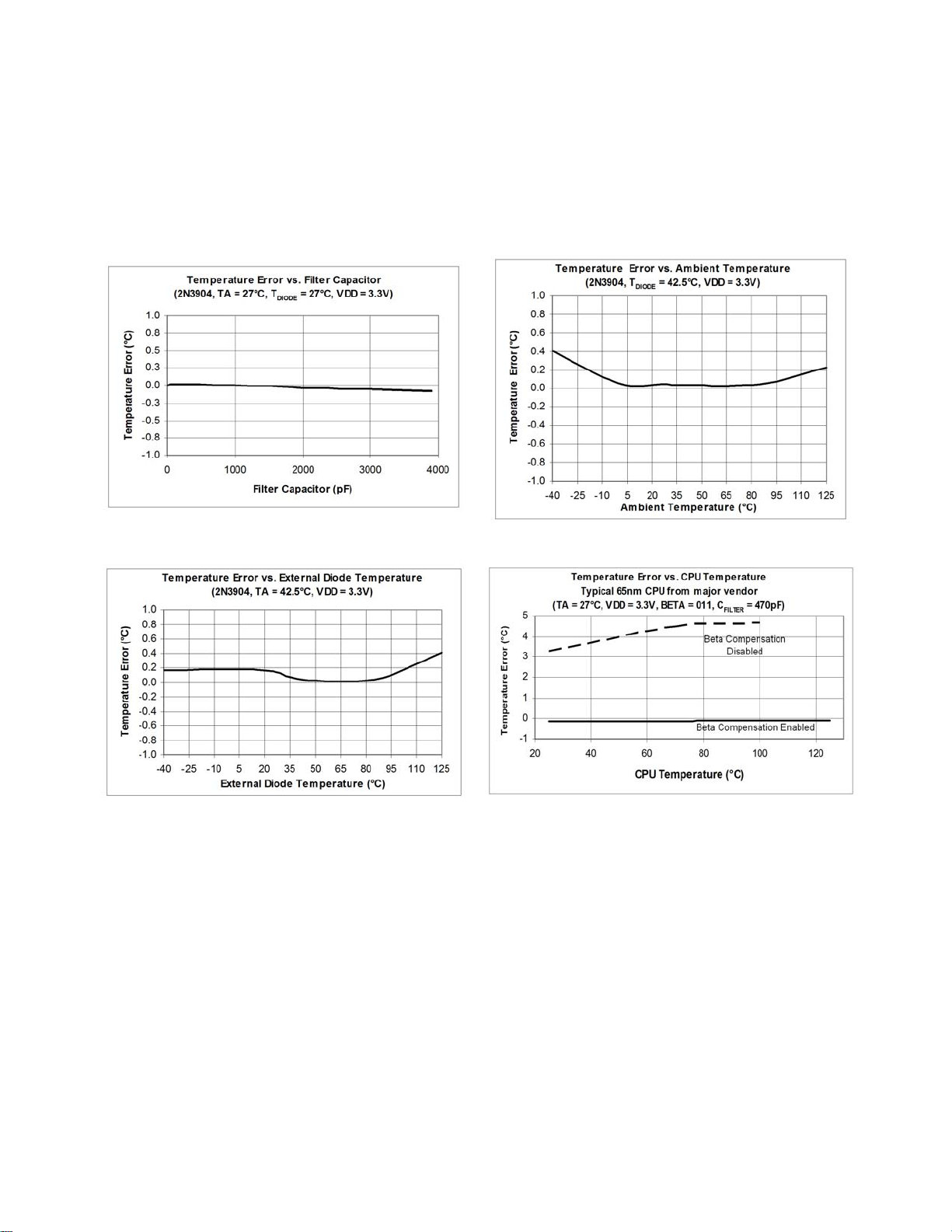
1°C Temperature Sensor with Beta Compensation
Data Sheet
Chapter 7 Typical Operating Curves
2014 Microchip Technology Inc. DS20005272A-page 45
Page 46
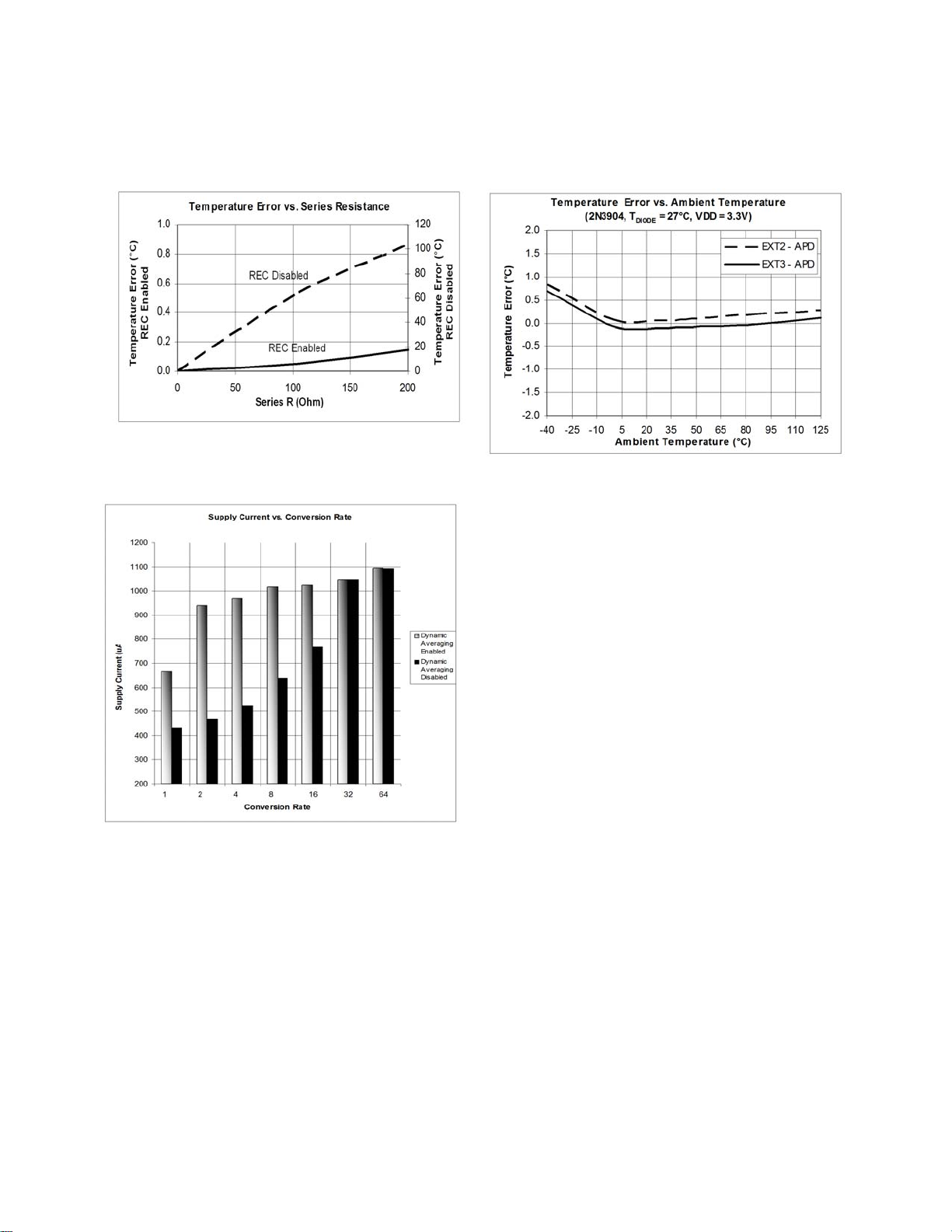
1°C Temperature Sensor with Beta Compensation
Data Sheet
DS20005272A-page 46 2014 Microchip Technology Inc.
Page 47
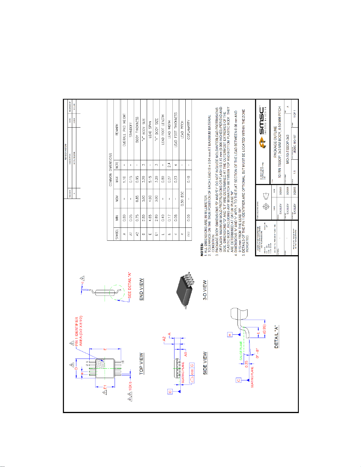
1°C Temperature Sensor with Beta Compensation
Data Sheet
Chapter 8 Package Information
Note: For the most current package drawings, see the Microchip Packaging Specification at
http://www.microchip.com/packaging.
Figure 8.1 10-Pin MSOP / TSSOP Package
2014 Microchip Technology Inc. DS20005272A-page 47
Page 48

1°C Temperature Sensor with Beta Compensation
Data Sheet
Note: For the most current package drawings,
see the Microchip Packaging Specification at
http://www.microchip.com/packaging
Figure 8.2 10-Pin DFN Package Drawing (1 of 2)
DS20005272A-page 48 2014 Microchip Technology Inc.
Page 49
1°C Temperature Sensor with Beta Compensation
Data Sheet
Note: For the most current package drawings,
see the Microchip Packaging Specification at
http://www.microchip.com/packaging
Figure 8.3 10-Pin DFN Package Dimensions (2 of 2)
2014 Microchip Technology Inc. DS20005272A-page 49
Page 50
1°C Temperature Sensor with Beta Compensation
Data Sheet
Note: For the most current package drawings,
see the Microchip Packaging Specification at
http://www.microchip.com/packaging
Figure 8.4 Package Drawing and PCB Footprint for SOIC-14
DS20005272A-page 50 2014 Microchip Technology Inc.
Page 51

1°C Temperature Sensor with Beta Compensation
Data Sheet
8.1 Package Markings
8.1.1 EMC1404-X-AIZL (10-pin MSOP)
All devices will be marked on the first line of the top side with “1404”. On the second line, they will be
marked with the appropriate -X number (-1, -2, etc), the Functional Revision “B” and Country Code
(CC).
8.1.2 EMC1403-X-AIZL (10-pin MSOP)
All devices will be marked on the first line of the top side with “1403”. On the second line, packages
will be marked with the appropriate -X number (-1, -2, etc), the Functional Revision “B” and Country
Code (CC).
8.1.3 EMC1403-1-AIA and EMC1403-2-AIA (10-pin DFN)
The EMC1403-1-AIA will be marked on the first line of the top side with the code “31” followed by the
first two characters of the last 6 characters of the Lot Number. The EMC1403-2-AIA is marked with
the code “32” followed by the first two characters of the last 6 characters of the Lot Number. On the
second line, packages will be marked with the last 4 characters of the Lot Number.
For example: If the Lot Number is “2H123456A”, the first line on the EMC1403-1-AIA will read “3123”
and the second line will read “456A”.
8.1.4 EMC1403-YZT
All devices will be marked on the first line of the top side with “EMC1403” followed by “-X” where X is
the appropriate -X number (-1, -2, etc). On the second line, packages will be marked with Functional
Revision “B”, date code and the last 7 characters of Lot Number.
2014 Microchip Technology Inc. DS20005272A-page 51
Page 52

1°C Temperature Sensor with Beta Compensation
Chapter 9 Data Sheet Revision History
Table 9.1 Revision History
REVISION LEVEL & DATE SECTION/FIGURE/ENTRY CORRECTION
REV A REV A replaces previous SMSC version Rev. 2.0 (08-10-12)
Data Sheet
Rev. 2.0 (08-10-12) Table 3.3, "SMBus Electrical
Specifications"
Section 6.21, "Revision
Register (FFh)"
Rev. 1.38 (02-28-12) Figure 2.2,
"EMC1403/EMC1404 Pin
Diagram, DFN-10"
Table 2.1, "EMC1403 and
EMC1404 Pin Description"
Rev. 1.37 (01-06-10) Section 8.1.4, "EMC1403-
YZT"
Section 8.1.3, "EMC1403-1-
AIA and EMC1403-2-AIA
(10-pin DFN)"
Rev. 1.36 (07-02-09) Table 2.1, "EMC1403 and
EMC1404 Pin Description"
Table 2.1, "EMC1403 and
EMC1404 Pin Description"
Added conditions for t
minimum of 0.3μs is required when receiving from
the master. Data hold time is 0μs min when
transmitting to the master.
Added row to indicate that revision ID can be 04h.
Revision ID may be 04h or 01h.
Added exposed pad and updated so it looks more
like a square.
Added last row for DFN bottom pad.
Recommendation is to connect it to ground.
Added to last sentence: “Revision “B”, date code
and the last 7 characters of” before “Lot Number”.
Corrected device code. Instead of being “32” for
both devices in the 10-pin DFN package, the code
is “31” for the EMC1403-1-AIA and “32” for the
EMC1403-2-AIA.
In pin description table, added to function column:
“requires pull-up resistor” for SMDATA and SMCLK
pins
Identified 5V tolerant pins. Added the following
application note below table: “For the 5V tolerant
pins that have a pull-up resistor (SMCLK,
SMDATA,
difference between VDD and the pull-up voltage
must never exceed 3.6V.”
THERM, and ALERT), the voltage
. Data hold time
HD:DAT
Table 3.1, "Absolute
Maximum Ratings"
Table 3.2, "Electrical
Specifications"
DS20005272A-page 52 2014 Microchip Technology Inc.
Updated voltage limits for 5V tolerant pins with
pull-up resistors.
Added the following note below table: “For the 5V
tolerant pins that have a pull-up resistor (SMCLK,
SMDATA,
voltage must not exceed 3.6V when the device is
unpowered.”
Added leakage current.
THERM, and ALERT), the pull-up
Page 53

1°C Temperature Sensor with Beta Compensation
Data Sheet
Table 9.1 Revision History (continued)
REVISION LEVEL & DATE SECTION/FIGURE/ENTRY CORRECTION
Rev. 1.35 (04-14-09) Figure 8.2, "10-Pin DFN
Package Drawing (1 of 2)"
Figure 8.3, "10-Pin DFN
Package Dimensions (2 of
2)"
Figure 8.4, "10 Pin DFN
PCB Footprint"
Table 3.1, "Absolute
Maximum Ratings"
Rev. 1.34 (02-27-09) Table 5.3, "Temperature
Data Format"
Rev. 1.33 (08-18-08) Ordering Information and
Table 1.1, "Part Selection"
Rev. 1.32 (07-10-08) Ordering Information and
Table 1.1, "Part Selection"
Rev. 1.31 (07-01-08) Ordering Information and
Table 1.1, "Part Selection"
Diagrams updated
Updated thermal resistance numbers
Extended range for -1 updated from 001 1111 1111
to 001 1111 1000
Added EMC1403-3 and EMC1403-4 for all
package options
Added EMC1404-4
Added EMC1404-2 and EMC1404-3
2014 Microchip Technology Inc. DS20005272A-page 53
Page 54

1°C Temperature Sensor with Beta Compensation
Data Sheet
Note the following details of the code protection feature on Microchip devices:
• Microchip products meet the specification contained in their particular Microchip Data Sheet.
• Microchip believes that its family of products is one of the most secure families of its kind on the market today, when used in the
intended manner and under normal conditions.
• There are dishonest and possibly illegal methods used to breach the code protection feature. All of these methods, to our
knowledge, require using the Microchip products in a manner outside the operating specifications contained in Microchip’s Data
Sheets. Most likely, the person doing so is engaged in theft of intellectual property.
• Microchip is willing to work with the customer who is concerned about the integrity of their code.
• Neither Microchip nor any other semiconductor manufacturer can guarantee the security of their code. Code protection does not
mean that we are guaranteeing the product as “unbreakable.”
Code protection is constantly evolving. We at Microchip are committed to continuously improving the code protection features of our
products. Attempts to break Microchip’s code protection feature may be a violation of the Digital Millennium Copyright Act. If such acts
allow unauthorized access to your software or other copyrighted work, you may have a right to sue for relief under that Act.
Information contained in this publication regarding device applications and the like is provided only for your convenience and may be
superseded by updates. It is your responsibility to ensure that your application meets with your specifications. MICROCHIP MAKES NO
REPRESENTATIONS OR WARRANTIES OF ANY KIND WHETHER EXPRESS OR IMPLIED, WRITTEN OR ORAL, STATUTORY OR
OTHERWISE, RELATED TO THE INFORMATION, INCLUDING BUT NOT LIMITED TO ITS CONDITION, QUALITY, PERFORMANCE,
MERCHANTABILITY OR FITNESS FOR PURPOSE. Microchip disclaims all liability arising from this information and its use. Use of
Microchip devices in life support and/or safety applications is entirely at the buyer’s risk, and the buyer agrees to defend, indemnify and
hold harmless Microchip from any and all damages, claims, suits, or expenses resulting from such use. No licenses are conveyed, implicitly or otherwise, under any Microchip intellectual property rights.
Trademarks
The Microchip name and logo, the Microchip logo, dsPIC, FlashFlex, KEELOQ, KEELOQ logo, MPLAB, PIC, PICmicro, PICSTART, PIC32
logo, rfPIC, SST, SST Logo, SuperFlash and UNI/O are registered trademarks of Microchip Technology Incorporated in the U.S.A. and
other countries.
FilterLab, Hampshire, HI-TECH C, Linear Active Thermistor, MTP, SEEVAL and The Embedded Control Solutions Company are
registered trademarks of Microchip Technology Incorporated in the U.S.A.
Silicon Storage Technology is a registered trademark of Microchip Technology Inc. in other countries.
Analog-for-the-Digital Age, Application Maestro, BodyCom, chipKIT, chipKIT logo, CodeGuard, dsPICDEM, dsPICDEM.net,
dsPICworks, dsSPEAK, ECAN, ECONOMONITOR, FanSense, HI-TIDE, In-Circuit Serial Programming, ICSP, Mindi, MiWi, MPASM,
MPF, MPLAB Certified logo, MPLIB, MPLINK, mTouch, Omniscient Code Generation, PICC, PICC-18, PICDEM, PICDEM.net, PICkit,
PICtail, REAL ICE, rfLAB, Select Mode, SQI, Serial Quad I/O, Total Endurance, TSHARC, UniWinDriver, WiperLock, ZENA and ZScale are trademarks of Microchip Technology Incorporated in the U.S.A. and other countries.
SQTP is a service mark of Microchip Technology Incorporated in the U.S.A.
GestIC and ULPP are registered trademarks of Microchip Technology Germany II GmbH & Co. KG, a subsidiary of Microchip
Technology Inc., in other countries.
A more complete list of registered trademarks and common law trademarks owned by Standard Microsystems Corporation (“SMSC”)
is available at: www.smsc.com. The absence of a trademark (name, logo, etc.) from the list does not constitute a waiver of any
intellectual property rights that SMSC has established in any of its trademarks.
All other trademarks mentioned herein are property of their respective companies.
© 2014, Microchip Technology Incorporated, Printed in the U.S.A., All Rights Reserved.
ISBN: 9781620779439
Microchip received ISO/TS-16949:2009 certification for its worldwide
headquarters, design and wafer fabrication facilities in Chandler and
Tempe, Arizona; Gresham, Oregon and design centers in California
and India. The Company’s quality system processes and procedures
are for its PIC
devices, Serial EEPROMs, microperipherals, nonvolatile memory and
analog products. In addition, Microchip’s quality system for the design
and manufacture of development systems is ISO 9001:2000 certified.
®
MCUs and dsPIC® DSCs, KEELOQ
®
code hopping
DS20005272A-page 54 2014 Microchip Technology Inc.
Page 55

Worldwide Sales and Service
AMERICAS
Corporate Office
2355 West Chandler Blvd.
Chandler, AZ 85224-6199
Tel: 480-792-7200
Fax: 480-792-7277
Technical Support:
http://www.microchip.com/
support
Web Address:
www.microchip.com
Atlanta
Duluth, GA
Tel: 678-957-9614
Fax: 678-957-1455
Austin, TX
Tel: 512-257-3370
Boston
Westborough, MA
Tel: 774-760-0087
Fax: 774-760-0088
Chicago
Itasca, IL
Tel: 630-285-0071
Fax: 630-285-0075
Cleveland
Independence, OH
Tel: 216-447-0464
Fax: 216-447-0643
Dallas
Addison, TX
Tel: 972-818-7423
Fax: 972-818-2924
Detroit
Novi, MI
Tel: 248-848-4000
Houston, TX
Tel: 281-894-5983
Indianapolis
Noblesville, IN
Tel: 317-773-8323
Fax: 317-773-5453
Los Angeles
Mission Viejo, CA
Tel: 949-462-9523
Fax: 949-462-9608
New York, NY
Tel: 631-435-6000
San Jose, CA
Tel: 408-735-9110
Canada - Toronto
Tel: 905-673-0699
Fax: 905-673-6509
ASIA/PACIFIC
Asia Pacific Office
Suites 3707-14, 37th Floor
Tower 6, The Gateway
Harbour City, Kowloon
Hong Kong
Tel: 852-2401-1200
Fax: 852-2401-3431
Australia - Sydney
Tel: 61-2-9868-6733
Fax: 61-2-9868-6755
China - Beijing
Tel: 86-10-8569-7000
Fax: 86-10-8528-2104
China - Chengdu
Tel: 86-28-8665-5511
Fax: 86-28-8665-7889
China - Chongqing
Tel: 86-23-8980-9588
Fax: 86-23-8980-9500
China - Hangzhou
Tel: 86-571-2819-3187
Fax: 86-571-2819-3189
China - Hong Kong SAR
Tel: 852-2943-5100
Fax: 852-2401-3431
China - Nanjing
Tel: 86-25-8473-2460
Fax: 86-25-8473-2470
China - Qingdao
Tel: 86-532-8502-7355
Fax: 86-532-8502-7205
China - Shanghai
Tel: 86-21-5407-5533
Fax: 86-21-5407-5066
China - Shenyang
Tel: 86-24-2334-2829
Fax: 86-24-2334-2393
China - Shenzhen
Tel: 86-755-8864-2200
Fax: 86-755-8203-1760
China - Wuhan
Tel: 86-27-5980-5300
Fax: 86-27-5980-5118
China - Xian
Tel: 86-29-8833-7252
Fax: 86-29-8833-7256
China - Xiamen
Tel: 86-592-2388138
Fax: 86-592-2388130
China - Zhuhai
Tel: 86-756-3210040
Fax: 86-756-3210049
ASIA/PACIFIC
India - Bangalore
Tel: 91-80-3090-4444
Fax: 91-80-3090-4123
India - New Delhi
Tel: 91-11-4160-8631
Fax: 91-11-4160-8632
India - Pune
Tel: 91-20-3019-1500
Japan - Osaka
Tel: 81-6-6152-7160
Fax: 81-6-6152-9310
Japan - Tokyo
Tel: 81-3-6880- 3770
Fax: 81-3-6880-3771
Korea - Daegu
Tel: 82-53-744-4301
Fax: 82-53-744-4302
Korea - Seoul
Tel: 82-2-554-7200
Fax: 82-2-558-5932 or
82-2-558-5934
Malaysia - Kuala Lumpur
Tel: 60-3-6201-9857
Fax: 60-3-6201-9859
Malaysia - Penang
Tel: 60-4-227-8870
Fax: 60-4-227-4068
Philippines - Manila
Tel: 63-2-634-9065
Fax: 63-2-634-9069
Singapore
Tel: 65-6334-8870
Fax: 65-6334-8850
Taiwan - Hsin Chu
Tel: 886-3-5778-366
Fax: 886-3-5770-955
Taiwan - Kaohsiung
Tel: 886-7-213-7830
Taiwan - Taipei
Tel: 886-2-2508-8600
Fax: 886-2-2508-0102
Thailand - Bangkok
Tel: 66-2-694-1351
Fax: 66-2-694-1350
EUROPE
Austria - Wels
Tel: 43-7242-2244-39
Fax: 43-7242-2244-393
Denmark - Copenhagen
Tel: 45-4450-2828
Fax: 45-4485-2829
France - Paris
Tel: 33-1-69-53-63-20
Fax: 33-1-69-30-90-79
Germany - Dusseldorf
Tel: 49-2129-3766400
Germany - Munich
Tel: 49-89-627-144-0
Fax: 49-89-627-144-44
Germany - Pforzheim
Tel: 49-7231-424750
Italy - Milan
Tel: 39-0331-742611
Fax: 39-0331-466781
Italy - Venice
Tel: 39-049-7625286
Netherlands - Drunen
Tel: 31-416-690399
Fax: 31-416-690340
Poland - Warsaw
Tel: 48-22-3325737
Spain - Madrid
Tel: 34-91-708-08-90
Fax: 34-91-708-08-91
Sweden - Stockholm
Tel: 46-8-5090-4654
UK - Wokingham
Tel: 44-118-921-5800
Fax: 44-118-921-5820
10/28/13
DS20005272A-page 55 2014 Microchip Technology Inc.
 Loading...