

Page 1

dsPICDEM™ 2
Development Board
User’s Guide
© 2005 Microchip Technology Inc. DS51558A
Page 2

Note the following details of the code protection feature on Microchip devices:
• Microchip products meet the specification contained in their particular Microchip Data Sheet.
• Microchip believes that its family of products is one of the most secure families of its kind on the market today, when used in the
intended manner and under normal conditions.
• There are dishonest and possibly illegal methods used to breach the code protection feature. All of these methods, to our
knowledge, require using the Microchip products in a manner outside the operating specifications contained in Microchip’s Data
Sheets. Most likely, the person doing so is engaged in theft of intellectual property.
• Microchip is willing to work with the customer who is concerned about the integrity of their code.
• Neither Microchip nor any other semiconductor manufacturer can guarantee the security of their code. Code protection does not
mean that we are guaranteeing the product as “unbreakable.”
Code protection is constantly evolving. We at Microchip are committed to continuously improving the code protection features of our
products. Attempts to break Microchip’s code protection feature may be a violation of the Digital Millennium Copyright Act. If such acts
allow unauthorized access to your software or other copyrighted work, you may have a right to sue for relief under that Act.
Information contained in this publication regarding device
applications and the like is provided only for your convenience
and may be superseded by updates. It is your responsibility to
ensure that your application meets with your specifications.
MICROCHIP MAKES NO REPRESENTATIONS OR WARRANTIES OF ANY KIND WHETHER EXPRESS OR IMPLIED,
WRITTEN OR ORAL, STATUTORY OR OTHERWISE,
RELATED TO THE INFORMATION, INCLUDING BUT NOT
LIMITED TO ITS CONDITION, QUALITY, PERFORMANCE,
MERCHANTABILITY OR FITNESS FOR PURPOSE.
Microchip disclaims all liability arising from this information and
its use. Use of Microchip’s products as critical components in
life support systems is not authorized except with express
written approval by Microchip. No licenses are conveyed,
implicitly or otherwise, under any Microchip intellectual property
rights.
Trademarks
The Microchip name and logo, the Microchip logo, Accuron,
dsPIC, K
EELOQ, microID, MPLAB, PIC, PICmicro, PICSTART,
PRO MATE, PowerSmart, rfPIC, and SmartShunt are
registered trademarks of Microchip Technology Incorporated
in the U.S.A. and other countries.
AmpLab, FilterLab, Migratable Memory, MXDEV, MXLAB,
PICMASTER, SEEVAL, SmartSensor and The Embedded
Control Solutions Company are registered trademarks of
Microchip Technology Incorporated in the U.S.A.
Analog-for-the-Digital Age, Application Maestro, dsPICDEM,
dsPICDEM.net, dsPICworks, ECAN, ECONOMONITOR,
FanSense, FlexROM, fuzzyLAB, In-Circuit Serial
Programming, ICSP, ICEPIC, Linear Active Thermistor,
MPASM, MPLIB, MPLINK, MPSIM, PICkit, PICDEM,
PICDEM.net, PICLAB, PICtail, PowerCal, PowerInfo,
PowerMate, PowerTool, rfLAB, rfPICDEM, Select Mode,
Smart Serial, SmartTel, Total Endurance and WiperLock are
trademarks of Microchip Technology Incorporated in the
U.S.A. and other countries.
SQTP is a service mark of Microchip Technology Incorporated
in the U.S.A.
All other trademarks mentioned herein are property of their
respective companies.
© 2005, Microchip Technology Incorporated, Printed in the
U.S.A., All Rights Reserved.
Printed on recycled paper.
Microchip received ISO/TS-16949:2002 quality system certification for
its worldwide headquarters, design and wafer fabrication facilities in
Chandler and Tempe, Arizona and Mountain View, California in
October 2003. The Company’s quality system processes and
procedures are for its PICmicro
devices, Serial EEPROMs, microperipherals, nonvolatile memory and
analog products. In addition, Microchip’s quality system for the design
and manufacture of development systems is ISO 9001:2000 certified.
®
8-bit MCUs, KEEL
®
OQ
code hopping
DS51558A-page ii © 2005 Microchip Technology Inc.
Page 3

dsPICDEM™ 2
DEVELOPMENT BOARD
USER’S GUIDE
Tabl e of Conten ts
Preface ........................................................................................................................... 1
Chapter 1. Introduction
1.1 Introduction ..................................................................................................... 7
1.2 Highlights ........................................................................................................ 7
1.3 dsPICDEM™ 2 Development Board .............................................................. 7
1.4 dsPICDEM™ 2 Development Board Resources ............................................ 8
1.5 Sample Application Projects ......................................................................... 12
1.6 Host System Environment ............................................................................ 12
Chapter 2. Getting Started
2.1 Introduction ................................................................................................... 13
2.2 Highlights ...................................................................................................... 13
2.3 Getting Started ............................................................................................. 13
2.4 Out-of-the-Box Demo ................................................................................... 14
2.5 Device Programming Process ...................................................................... 17
2.6 In-Circuit Debugging Process ....................................................................... 19
2.7 Summary ...................................................................................................... 20
Chapter 3. Using the dsPIC30F2010
3.1 Introduction ................................................................................................... 21
3.2 Highlights ...................................................................................................... 21
3.3 Board Setup for the dsPIC30F2010 Sample Application ............................. 21
3.4 Device Programming .................................................................................... 23
3.5 Observing the Sample Application ............................................................... 24
3.6 In-Circuit Debugging ..................................................................................... 25
3.7 Summary ...................................................................................................... 26
Chapter 4. Using the dsPIC30F2011
4.1 Introduction ................................................................................................... 27
4.2 Highlights ...................................................................................................... 27
4.3 Board Setup for the dsPIC30F2011 Sample Application ............................. 27
4.4 Device Programming .................................................................................... 29
4.5 Observing the Sample Application ............................................................... 30
4.6 In-Circuit debugging ..................................................................................... 31
4.7 Summary ...................................................................................................... 32
Chapter 5. Using the dsPIC30F2012
5.1 Introduction ................................................................................................... 33
5.2 Highlights ...................................................................................................... 33
5.3 Board Setup for the dsPIC30F2012 Sample Application ............................. 33
5.4 Device Programming .................................................................................... 35
© 2005 Microchip Technology Inc. DS51558A-page i
Page 4

dsPICDEM 2 Development Board User’s Guide
5.5 Observing the Sample Application ............................................................... 36
5.6 In-Circuit Debugging ..................................................................................... 37
5.7 Summary ...................................................................................................... 38
Chapter 6. Using the dsPIC30F3010
6.1 Introduction ................................................................................................... 39
6.2 Highlights ...................................................................................................... 39
6.3 Board Setup for the dsPIC30F3010 Sample Application ............................. 39
6.4 Device Programming .................................................................................... 41
6.5 Observing the Sample Application ............................................................... 42
6.6 In-Circuit Debugging ..................................................................................... 43
6.7 Summary ...................................................................................................... 44
Chapter 7. Using the dsPIC30F3011
7.1 Introduction ................................................................................................... 45
7.2 Highlights ...................................................................................................... 45
7.3 Board Setup for the dsPIC30F3011 Sample Application ............................. 45
7.4 Device Programming .................................................................................... 47
7.5 Observing the Sample Application ............................................................... 48
7.6 In-Circuit Debugging ..................................................................................... 49
7.7 Summary ...................................................................................................... 50
Chapter 8. Using the dsPIC30F3012
8.1 Introduction ................................................................................................... 51
8.2 Highlights ...................................................................................................... 51
8.3 Board Setup for the dsPIC30F3012 Sample Application ............................. 51
8.4 Device Programming .................................................................................... 53
8.5 Observing the Sample Application ............................................................... 54
8.6 In-Circuit Debugging ..................................................................................... 55
8.7 Summary ...................................................................................................... 56
Chapter 9. Using the dsPIC30F3013
9.1 Introduction ................................................................................................... 57
9.2 Highlights ...................................................................................................... 57
9.3 Board Setup for the dsPIC30F3013 Sample Application ............................. 57
9.4 Device Programming .................................................................................... 59
9.5 Observing the Sample Application ............................................................... 60
9.6 In-Circuit Debugging ..................................................................................... 61
9.7 Summary ...................................................................................................... 62
Chapter 10. Using the dsPIC30F3014
10.1 Introduction ................................................................................................. 63
10.2 Highlights .................................................................................................... 63
10.3 Board Setup for the dsPIC30F3014 Sample Application ........................... 63
10.4 Device Programming .................................................................................. 65
10.5 Observing the Sample Application ............................................................. 66
10.6 In-Circuit Debugging ................................................................................... 67
10.7 Summary .................................................................................................... 68
DS51558A-page ii © 2005 Microchip Technology Inc.
Page 5

Chapter 11. Using the dsPIC30F4011
11.1 Introduction ................................................................................................. 69
11.2 Highlights .................................................................................................... 69
11.3 Board Setup for the dsPIC30F4011 Sample Application ........................... 69
11.4 Device Programming .................................................................................. 71
11.5 Observing the Sample Application ............................................................. 72
11.6 In-Circuit Debugging ................................................................................... 73
11.7 Summary .................................................................................................... 74
Chapter 12. Using the dsPIC30F4012
12.1 Introduction ................................................................................................. 75
12.2 Highlights .................................................................................................... 75
12.3 Board Setup for the dsPIC30F4012 Sample Application ........................... 75
12.4 Device Programming .................................................................................. 77
12.5 Observing the Sample Application ............................................................. 78
12.6 In-Circuit Debugging ................................................................................... 79
12.7 Summary .................................................................................................... 80
Chapter 13. Using the dsPIC30F4013
13.1 Introduction ................................................................................................. 81
13.2 Highlights .................................................................................................... 81
13.3 Board Setup for the dsPIC30F4013 Sample Application ........................... 81
13.4 Device Programming .................................................................................. 83
13.5 Observing the Sample Application ............................................................. 84
13.6 In-Circuit Debugging ................................................................................... 85
13.7 Summary .................................................................................................... 86
Chapter 14. Hardware
14.1 Hardware Overview .................................................................................... 87
Appendix A. Hardware Drawings and Schematics
A.1 Introduction .................................................................................................. 95
Appendix B. Writing to LCD
B.1 Overview .................................................................................................... 103
B.2 LCD Hardware Setup ................................................................................. 103
B.3 LCD Software Specification ....................................................................... 103
B.4 LCD Firmware Programming: .................................................................... 104
Appendix C. Board Errata
C.1 H7 and H6 Labelling Error ......................................................................... 105
Index ........................................................................................................................... 107
Worldwide Sales and Service .................................................................................. 114
© 2005 Microchip Technology Inc. DS51558A-page iii
Page 6

dsPICDEM 2 Development Board User’s Guide
DS51558A-page iv © 2005 Microchip Technology Inc.
Page 7

dsPICDEM™ 2
DEVELOPMENT BOARD
USER’S GUIDE
Preface
NOTICE TO CUSTOMERS
All documentation becomes dated, and this manual is no exception. Microchip tools and
documentation are constantly evolving to meet customer needs, so some actual dialogs
and/or tool descriptions may differ from those in this document. Please refer to our web site
(www.microchip.com) to obtain the latest documentation available, including errata
documents applicable to this product. Also, refer to the errata information in Appendix C.
Documents are identified with a “DS” number. This number is located on the bottom of each
page, in front of the page number. The numbering convention for the DS number is
“DSXXXXXA”, where “XXXXX” is the document number and “A” is the revision level of the
document.
For the most up-to-date information on development tools, see the MPLAB
Select the Help menu, and then Topics to open a list of available on-line help files.
®
IDE on-line help.
INTRODUCTION
This chapter contains general information that will be useful to know before using the
dsPICDEM 2 Development Board. Items discussed in this chapter include:
• Document Layout
• Conventions Used in this Guide
• Warranty Registration
• Recommended Reading
• The Microchip Web Site
• Development Systems Customer Change Notification Service
• Customer Support
• Document Revision History
DOCUMENT LAYOUT
This document describes how to use dsPICDEM 2 Development Board as a development tool to emulate and debug firmware on a target board. The manual layout is as
follows:
• Chapter 1. Introduction – This chapter introduces the dsPICDEM 2
Development Board, provides a brief description of the hardware components on
the board and introduces the demonstration software provided with each of the
supported dsPIC30F devices.
• Chapter 2. Getting Started – This chapter describes the out-of-the-box operation
of the dsPICDEM 2 Development Board. It also provides a detailed descripton of
how to perform programming and in-circuit debugging operations.
• Chapter 3. Using the dsPIC30F2010 – This chapter describes how to configure
the dsPICDEM 2 Development Board for use with the dsPIC30F2010 Digital
Signal Controller. It provides suggested procedures for device programming and
in-circuit debugging of the dsPIC30F2010 using the sample application.
© 2005 Microchip Technology Inc. DS51558A-page 1
Page 8

dsPICDEM 2 Development Board User’s Guide
• Chapter 4. Using the dsPIC30F2011 – This chapter describes how to configure
the dsPICDEM 2 Development Board for use with the dsPIC30F2011 Digital
Signal Controller. It provides suggested procedures for device programming and
in-circuit debugging of the dsPIC30F2011using the sample application.
• Chapter 5. Using the dsPIC30F2012 – This chapter describes how to configure
the dsPICDEM 2 Development Board for use with the dsPIC30F2012 Digital
Signal Controller. It provides suggested procedures for device programming and
in-circuit debugging of the dsPIC30F2012 using the sample application.
• Chapter 6. Using the dsPIC30F3010 – This chapter describes how to configure
the dsPICDEM 2 Development Board for use with the dsPIC30F3010 Digital
Signal Controller. It provides suggested procedures for device programming and
in-circuit debugging of the dsPIC30F3010 using the sample application.
• Chapter 7. Using the dsPIC30F3011 – This chapter describes how to configure
the dsPICDEM 2 Development Board for use with the dsPIC30F3011 Digital
Signal Controller. It provides suggested procedures for device programming and
in-circuit debugging of the dsPIC30F3011 using the sample application.
• Chapter 8. Using the dsPIC30F3012 – This chapter describes how to configure
the dsPICDEM 2 Development Board for use with the dsPIC30F3012 Digital
Signal Controller. It provides suggested procedures for device programming and
in-circuit debugging of the dsPIC30F3012 using the sample application.
• Chapter 9. Using the dsPIC30F3013 – This chapter describes how to configure
the dsPICDEM 2 Development Board for use with the dsPIC30F3013 Digital
Signal Controller. It provides suggested procedures for device programming and
in-circuit debugging of the dsPIC30F3013 using the sample application.
• Chapter 10. Using the dsPIC30F3014 – This chapter describes how to configure
the dsPICDEM 2 Development Board for use with the dsPIC30F3014 Digital
Signal Controller. It provides suggested procedures for device programming and
in-circuit debugging of the dsPIC30F3014 using the sample application.
• Chapter 11. Using the dsPIC30F4011 – This chapter describes how to configure
the dsPICDEM 2 Development Board for use with the dsPIC30F4011 Digital
Signal Controller. It provides suggested procedures for device programming and
in-circuit debugging of the dsPIC30F4011 using the sample application.
• Chapter 12. Using the dsPIC30F4012 – This chapter describes how to configure
the dsPICDEM 2 Development Board for use with the dsPIC30F4012 Digital
Signal Controller. It provides suggested procedures for device programming and
in-circuit debugging of the dsPIC30F4012 using the sample application.
• Chapter 13. Using the dsPIC30F4013 – This chapter describes how to configure
the dsPICDEM 2 Development Board for use with the dsPIC30F4013 Digital
Signal Controller. It provides suggested procedures for device programming and
in-circuit debugging of the dsPIC30F4013 using the sample application.
• Chapter 14. Hardware – This chapter provides detailed information related to the
hardware components used on the dsPICDEM 2 Development Board.
• Appendix A. Hardware Drawings and Schematics – This appendix illustrates
the dsPICDEM 2 Development Board layout and includes complete schematic
diagrams.
• Appendix B. Writing to LCD – This appendix provides detailed instructions for
writing to the 2 x 16 character LCD.
• Appendix C. Board Errata – This appendix describes errata associated with
certain revisions of the dsPICDEM 2 Development Board.
• Index – This section provides cross-reference listing of terms, features and
sections of this document.
• Worldwide Sales and Service – A listing of Microchip sales and service locations
and telephone numbers worldwide.
DS51558A-page 2 © 2005 Microchip Technology Inc.
Page 9

CONVENTIONS USED IN THIS GUIDE
This manual uses the following documentation conventions:
DOCUMENTATION CONVENTIONS
Description Represents Examples
Arial font:
Italic characters Referenced books
Initial caps A window the Output window
Quotes A field name in a window or
Underlined, italic text with
right angle bracket
Bold characters A dialog button Click OK
‘b
nnnn
Text in angle brackets < > A key on the keyboard Press <Enter>, <F1>
Courier font:
Plain Courier Sample source code #define START
Italic Courier A variable argument file.o, where file can be
0xnnnn A hexadecimal number where
Square brackets [ ] Optional arguments mcc18 [options] file
Curly brackets and pipe
character: { | }
Ellipses... Replaces repeated text var_name [,
Preface
MPLAB® IDE User’s Guide
Emphasized text ...is the
A dialog the Settings dialog
A menu selection select Enable Programmer
“Save project before build”
dialog
A menu path
A tab Click the Power tab
A binary number where n is a
digit
Filenames autoexec.bat
File paths c:\mcc18\h
Keywords _asm, _endasm, static
Command-line options -Opa+, -Opa-
Bit values 0, 1
n is a hexadecimal digit
Choice of mutually exclusive
arguments; an OR selection
Represents code supplied by
user
File>Save
‘b00100, ‘b10
any valid filename
0xFFFF, 0x007A
[options]
errorlevel {0|1}
var_name...]
void main (void)
{ ...
}
only
compiler...
© 2005 Microchip Technology Inc. DS51558A-page 3
Page 10

dsPICDEM 2 Development Board User’s Guide
WARRANTY REGISTRATION
Please complete the enclosed Warranty Registration Card and mail it promptly.
Sending in the Warranty Registration Card entitles users to receive new product
updates. Interim software releases are available at the Microchip web site.
RECOMMENDED READING
This user's guide describes how to use dsPICDEM 2 Development Board. Other useful
documents are listed below. The following Microchip documents are available and recommended as supplemental reference resources.
dsPIC30F Family Reference Manual (DS70046)
Consult this document for detailed information on the dsPIC30F device operation. The
manual explains the operation of the dsPIC30F MCU family architecture and peripheral
modules but does not cover the specifics of each device. Refer to the appropriate
device data sheet, mentioned below, for device-specific information.
dsPIC30F Data Sheet, Motor Control and Power Conversion Family (DS70082)
Consult this document for information regarding the dsPIC30F Motor Control and
Power Conversion devices. Reference information found in this data sheet includes:
• Device memory map
• Device pinout and packaging details
• Device electrical specifications
• List of peripherals included on the device
dsPIC30F Data Sheet, General Purpose and Sensor Families (DS70083)
Consult this document for information regarding the dsPIC30F General Purpose and
Sensor devices. Reference information found in this data sheet includes:
• Device memory map
• Device pinout and packaging details
• Device electrical specifications
• List of peripherals included on the device
dsPIC30F Programmer’s Reference Manual (DS70030)
This manual is a software developer’s reference for the dsPIC30F 16-bit MCU family
of devices. This manual describes the instruction set in detail and also provides general
information to assist the user in developing software for the dsPIC30F MCU family.
dsPIC30F Family Overview, dsPIC
16-bit Digital Signal Controller (DS70043)
This document provides an overview of the features and functionality of the dsPIC DSC
product family. It helps determine how the dsPIC 16-bit Digital Signal Controller Family
fits a specific product application. For detailed information about any of the functionality,
refer to the
MPLAB
This document details Microchip Technology’s language tools for dsPIC DSC devices
based on GNU technology. The language tools discussed are:
• MPLAB ASM30 Assembler
• MPLAB LINK30 Linker
• MPLAB LIB30 Archiver/Librarian
• Other Utilities
dsPIC30F Family Reference Manual
®
ASM30, MPLAB LINK30 and Utilities User’s Guide (DS51317)
®
High Performance
(DS70046).
DS51558A-page 4 © 2005 Microchip Technology Inc.
Page 11

MPLAB® C30 C Compiler User’s Guide (DS51284)
The purpose of this document is to help you use Microchip’s MPLAB C30 C compiler
for dsPIC DSC devices to develop your application. MPLAB C30 is a GNU-based language tool, based on source code from the Free Software Foundation (FSF). For more
information about the FSF, see www.fsf.org.
Other GNU language tools available from Microchip are:
• MPLAB ASM30 Assembler
• MPLAB LINK30 Linker
• MPLAB LIB30 Librarian/Archiver
MPLAB
Consult this document for more information pertaining to the installation and features
of the MPLAB Integrated Development Environment (IDE) Software.
To obtain any of these documents, contact the nearest Microchip sales location
(see back page) or visit the Microchip web site at: www.microchip.com.
®
IDE Simulator, Editor User’s Guide (DS51025)
THE MICROCHIP WEB SITE
Microchip provides online support via our web site at www.microchip.com. This web
site is used as a means to make files and information easily available to customers.
Accessible by using your favorite Internet browser, the web site contains the following
information:
• Product Support – Data sheets and errata, application notes and sample
programs, design resources, user’s guides and hardware support documents,
latest software releases and archived software
• General Technical Support – Frequently Asked Questions (FAQs), technical
support requests, online discussion groups, Microchip consultant program
member listing
• Business of Microchip – Product selector and ordering guides, latest Microchip
press releases, listing of seminars and events, listings of Microchip sales offices,
distributors and factory representatives
Preface
DEVELOPMENT SYSTEMS CUSTOMER CHANGE NOTIFICATION SERVICE
Microchip’s customer notification service helps keep customers current on Microchip
products. Subscribers will receive e-mail notification whenever there are changes,
updates, revisions or errata related to a specified product family or development tool of
interest.
To register, access the Microchip web site at www.microchip.com, click on Customer
Change Notification and follow the registration instructions.
The Development Systems product group categories are:
• Compilers – The latest information on Microchip C compilers and other language
tools. These include the MPLAB C18 and MPLAB C30 C compilers; MPASM™
and MPLAB ASM30 assemblers; MPLINK™ and MPLAB LINK30 object linkers;
and MPLIB™ and MPLAB LIB30 object librarians.
• Emulators – The latest information on Microchip in-circuit emulators.This
includes the MPLAB ICE 2000 and MPLAB ICE 4000.
• In-Circuit Debuggers – The latest information on the Microchip in-circuit
debugger, MPLAB ICD 2.
© 2005 Microchip Technology Inc. DS51558A-page 5
Page 12

dsPICDEM 2 Development Board User’s Guide
• MPLAB® IDE – The latest information on Microchip MPLAB IDE, the Windows®
Integrated Development Environment for development systems tools. This list is
focused on the MPLAB IDE, MPLAB SIM simulator, MPLAB IDE Project Manager
and general editing and debugging features.
• Programmers – The latest information on Microchip programmers. These include
the MPLAB PM3 and PRO MATE
Plus and PICkit
CUSTOMER SUPPORT
Users of Microchip products can receive assistance through several channels:
• Distributor or Representative
• Local Sales Office
• Field Application Engineer (FAE)
• Technical Support
• Development Systems Information Line
Customers should contact their distributor, representative or field application engineer
(FAE) for support. Local sales offices are also available to help customers. A listing of
sales offices and locations is included in the back of this document.
Technical support is available through the web site at: http://support.microchip.com
In addition, there is a Development Systems Information Line which lists the latest
versions of Microchip's development systems software products. This line also
provides information on how customers can receive currently available upgrade kits.
The Development Systems Information Line numbers are:
1-800-755-2345 – United States and most of Canada
1-480-792-7302 – Other International Locations
Customers may also exchange ideas with each other and with Microchip personnel by
logging on to http:\\forum.microchip.com.
®
1 development programmers.
®
II device programmers and the PICSTART®
DOCUMENT REVISION HISTORY
Revision A (June 2005)
• Initial Release of this Document.
DS51558A-page 6 © 2005 Microchip Technology Inc.
Page 13

1.1 INTRODUCTION
The dsPICDEM™ 2 Development Board is a development and evaluation tool that
helps you create embedded applications using dsPIC30F Digital Signal Controllers
(DSC) in 18-pin PDIP, 28-pin SPDIP and 40-pin PDIP packages. The dsPICDEM™ 2
Development Board provides both a hardware and software baseline capability to help
jump start your application.
Sockets are provided for 28 and 40-pin devices in the dsPIC30F Motor Control family
and 18, 28 and 40-pin devices in the dsPIC30F General Purpose and Sensor family.
For each device supported by the board, the product CD includes a sample application
program designed specifically for that device. Thus, regardless of the dsPIC30F device
you choose for your application, you also have sample code appropriate to that device.
1.2 HIGHLIGHTS
This chapter discusses:
• dsPICDEM™ 2 Development Board
• dsPICDEM™ 2 Development Board Resources
• Sample Application Projects
• Host System Environment
dsPICDEM™ 2
DEVELOPMENT BOARD
USER’S GUIDE
Chapter 1. Introduction
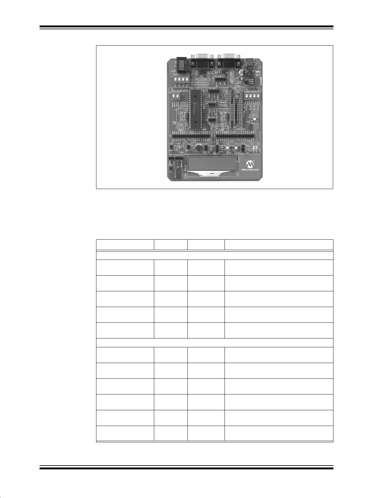
1.3 dsPICDEM™ 2 DEVELOPMENT BOARD
The dsPICDEM™ 2 Development Board (Figure 1-1) includes a dsPIC30F4011 Digital
Signal Processor in the 40-pin motor control socket, a power supply regulator, crystal
oscillators for each set of sockets, an ICD header for the MPLAB ICD 2 In-Circuit
Debugger and both UART and CAN ports for external communication. In addition, the
board is populated with prototyping hardware, including LED indicators, push-button
switches, a potentiometer, a temperature sensor and an LCD screen. All pins on all the
device sockets are accessible on prototyping areas. Also included is the dsPICDEM™
2 Development Kit CD, which contains software and this User’s Guide.
Key hardware features include:
• Multiple sockets for 18, 28 and 40-pin PDIP and SPDIP devices
• dsPIC30F4011 40-pin PDIP sample device installed on the board
• 5V regulator provides V
indicates when the power is on.
• Connector for MPLAB
Emulator
• RS-232 interface
• Controller Area Network (CAN) interface
• Temperature sensor and analog potentiometer to simulate A/D inputs
• Pushbutton switches and LED indicators to simulate digital input and output
• 2x16 ASCII Character LCD with SPI™ interface
• 2x20 prototyping header area for user hardware expansion (header not provided)
DD and AVDD from a 9V DC power supply. An LED
®
ICD 2 In-Circuit Debugger or MPLAB ICE 4000 In-Circuit
© 2005 Microchip Technology Inc. DS51558A-page 7
Page 14
dsPICDEM 2 Development Board User’s Guide
FIGURE 1-1: dsPICDEM™ 2 DEVELOPMENT BOARD
1.4 dsPICDEM™ 2 DEVELOPMENT BOARD RESOURCES
The dsPICDEM™ 2 Development Board accommodates the devices listed in
Ta bl e 1 - 1.
TABLE 1-1: DEVICES SUPPORTED BY dsPICDEM™ 2
dsPIC30F Device Pins Socket Resources
Motor Control Family
2010 28 U2B1 Six 10-bit A/D (500 ksps) channels,
UART, SPI, I2C™ and 20 I/O pins*
3010 28 U2B1 Six 10-bit A/D (500 ksps) channels,
UART, SPI, I
3011 40 U2A1 Nine 10-bit A/D (500 ksps) channels, two
UARTs, SPI, I
4011 40 U2A1 Nine 10-bit A/D (500 ksps) channels, two
UARTs, SPI, I
4012 28 U2B1 Six 10-bit A/D (500 ksps) channels,
UART, SPI, I
General Purpose and Sensor Family
2011 18 U1C1 Eight 12-bit A/D (100 ksps) channels,
UART, SPI, I
3012 18 U1C1 Eight 12-bit A/D (100 ksps) channels,
UART, SPI, I
2012 28 U1B1 Ten 12-bit A/D (100 ksps) channels,
UART, SPI, I
3013 28 U1B1 Ten 12-bit A/D (100 ksps) channels, two
UARTs, SPI, I
3014 40 U1A1 13 12-bit A/D (100 ksps) channels, two
UARTs, SPI, I
4013 40 U1A1 13 12-bit A/D (100 ksps) channels, two
UARTs, SPI, I
* Includes pins shared by the peripheral functions
2
C and 20 I/O pins*
2
C and 30 I/O pins*
2
C, CAN and 30 I/O pins*
2
C, CAN and 20 I/O pins*
2
C and 12 I/O pins*
2
C and 12 I/O pins*
2
C and 20 I/O pins*
2
C and 20 I/O pins*
2
C and 30 I/O pins*
2
C, CAN and 30 I/O pins*
DS51558A-page 8 © 2005 Microchip Technology Inc.
Page 15
Introduction
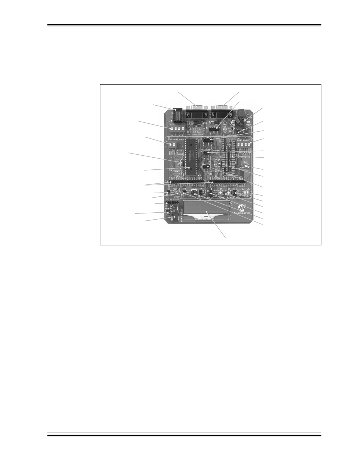
The dsPICDEM™ 2 must be configured for the device you have chosen for your application. Switches and headers are provided to connect hardware components on the
board with corresponding pins on the dsPIC30F device. Figure 1-2 shows the location
of hardware components and configuration headers that need to be set up depending
on the dsPIC30F device.
FIGURE 1-2: dsPICDEM™ 2 HARDWARE COMPONENTS
UART Connection (J2)
CAN Connection (J3)
MPLAB® Programmer
/Debugger Connection (J1)
Selector S2 (for programming
and debugging)
Selector S3 (for debugging
motor control devices)
Oscillator for motor control
device (Y2)
Concentric sockets for
motor control devices
(U2A1 & U2B1 under
dsPIC30F4011)
External connection prototyping
headers (H8 and H9)
Temperature Header (H10)
Temperature Sensor (U5)
LCD SPI Header (H1)
LCD Controller Programming
Header (H11)
SPI™ controller for LCD
CAN Header (H2)
Power Supply
Power Supply jumpers
(JP1 and JP2)
UART1 Header (H3)
Selector (S4) for debugging
general purpose devices
Alternate UART1 Header (H4)
Concentric sockets for
General Purpose devices
(U1A1, U1B1, U1C1)
Reset switch (S1)
Oscillator for General
Purpose device (Y5)
UART2 Header (H5)
Output LEDs (D3 and D4)
LED Header (H12)
Switches (S5 and S6)
Switches Header (H6 and H7)
Analog Pot (R15)
Pot Header (H13)
LCD (LCD1)
1.4.1 dsPIC30F Device Sockets
For convenience, the board provides separate sockets for Motor Control family devices
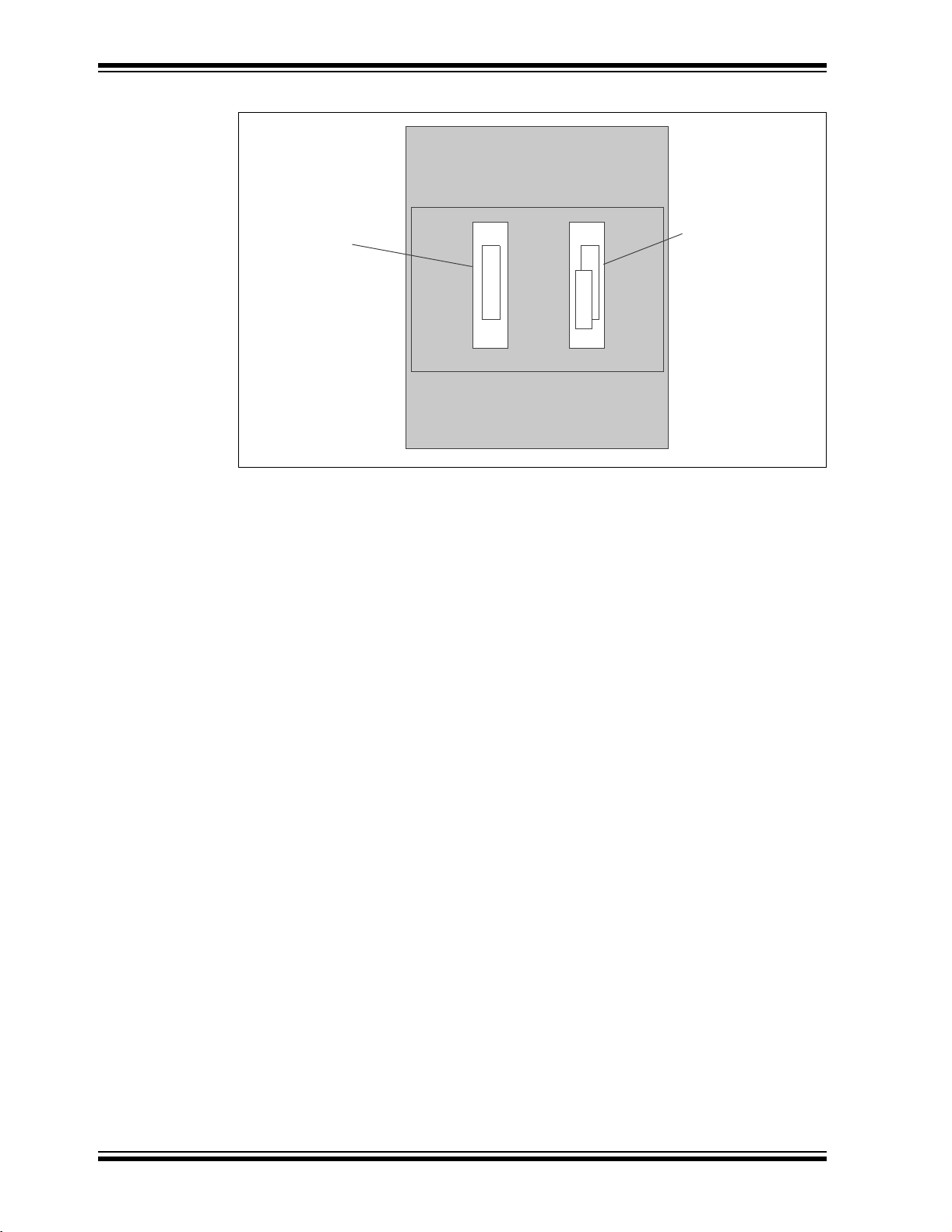
and general purpose/sensor family devices. As shown in Figure 1-3, the left side of the
board includes concentric sockets (U2B1 and U2A1) for 28 and 40-pin devices, respectively, in the Motor Control family. The right side includes concentric sockets (U1C1,
U1B1 and U1A1) for 18, 28 and 40-pin devices, respectively, in the General Purpose
and Sensor family.
© 2005 Microchip Technology Inc. DS51558A-page 9
Page 16
dsPICDEM 2 Development Board User’s Guide
FIGURE 1-3: dsPICDEM™ 2 DEVELOPMENT BOARD LAYOUT
Sockets for Motor
Control Family
Devices:
dsPIC30F2010
dsPIC30F3010
dsPIC30F3011
dsPIC30F4011
dsPIC30F4012
U2A1
U2B1
U1A1
U1B1
U1C1
Sockets for General
Purpose and Sensor
Family Devices:
dsPIC30F2011
dsPIC30F3012
dsPIC30F2012
dsPIC30F3013
dsPIC30F3014
dsPIC30F4013
1.4.2 MPLAB ICD 2 Header
An RJ11 connector (J1) allows the MPLAB ICD 2 Debugger/Programmer to be used
with the dsPIC30F device you have plugged into the board. Switches S2, S3 and S4
physically connect this interface to the device sockets. Switch S2 connects the MPLAB
ICD 2 interface to the default programming and debugging pins on the dsPIC30F
devices (PGC/EMUC and PGD/EMUD). This switch should be turned on during
programming.
Switches S3 and S4 connect the MPLAB ICD 2 interface to alternative debugging pins
on the dsPIC30F devices (EMUC1/EMUD1 and EMUC2/EMUD2). These switches
should be turned off during device programming and turned on during debugging, if
needed.
1.4.3 UART Connection
A DB9 connector (J2) facilitates external RS-232RS-232 communication. Headers H3,
H4 and H5 connect this interface to the UART peripheral in the dsPIC DSC device.
Header H3 selects UART1. Header H4 selects alternate pins for UART1 in all
dsPIC30F devices supported by this board. Header H5 selects UART2 in dsPIC30F
devices that provide two UARTs (dsPIC30F3011, 3013, 3014, 4011 and 4013).
1.4.4 CAN Connection
A second DB9 connector (J3) is used for CAN communication. Header H2 selects the
dsPIC DSC device for the CAN interface. The CAN interface is supported by
dsPIC30F4011, 4012 and 4013 devices.
1.4.5 Power Supply
The dsPICDEM™ 2 power supply IS powered from an AC/DC wall adapter that
furnishes 9 VDC to the PWR jack (J4). The power supply is split at the regulator to
provide a separate, de-coupled analog supply voltage useful in designs taking
advantage of the dsPIC30F A/D converters. The power supply includes an on-board
+5V regulator for supplying V
Jumpers (JP1 and JP2) let you disconnect the power supply from the board if you want
to supply external DC power via terminals TP1 and TP2.
DS51558A-page 10 © 2005 Microchip Technology Inc.
DD and AVDD. An LED indicates when the power is on.
Page 17

Introduction
1.4.6 Reset Switch
This pushbutton switch (S1) is tied to the MCLR pin on the dsPIC30F device. It is used
to reset the device regardless of the socket used.
1.4.7 Device Clocking
Device clocking can be provided by on-chip RC oscillators, on-board crystal oscillators
or external sources. Crystal (Y1) provides a 7.3728 MHz oscillator for the motor control
device. Crystal (Y2) provides a 7.3728 MHz oscillator for the general purpose and
sensor devices.
1.4.8 Analog and Digital Inputs
The dsPICDEM™ 2 provides the following sensors that can be used to provide input
signals to your application program:
• Temperature sensor (U5)
• Potentiometer (R15)
• Pushbutton switches (S5 and S6)
1.4.8.1 TEMPERATURE SENSOR
The temperature sensor is a TC1047A that provides an analog signal to analog
channel AN3 in either the general purpose or motor control device via header H10.
1.4.8.2 ANALOG POTENTIOMETER
A 5-kOhm potentiometer provides an analog signal to analog channel AN2 in either the
general purpose or motor control device via header H13. The voltage source to the
potentiometer is provided by VR1, through a low-pass filter. VR1 is the main voltage
regulator for all components on the development board.
1.4.8.3 PUSHBUTTON SWITCHES
Two pushbutton switches, S5 and S6, are connected to external interrupt pins INT0 and
INT1, respectively, on the dsPIC30F device via headers H6 and H7, respectively.
1.4.9 Digital Outputs
The dsPICDEM™ 2 provides the following output devices that can be used to display
output information from your application program:
• LED Indicators (D3 and D4)
• LCD Display (LCD1/LCD2)
1.4.9.1 LED INDICATORS
LEDs D3 and D4 are connected to port pins RB0 and RB1, respectively on the installed
dsPIC DSC device via header H12. The LED anodes are tied to VDD through a 1.2K
resistor.
1.4.9.2 LCD DISPLAY
A 2 x 16 character dot matrix LCD display is provided on the development board. The
installed dsPIC30F device writes characters to the LCD via the clock (SCK1) and data
(SDO1) pins on the device’s SPI1 module.
1.4.10 External Connections
Prototyping areas H8 and H9 provide external connections from the motor control and
general purpose devices, respectively. These connections allow you to use hardware
and test equipment not provided on the dsPICDEM™ 2 board.
© 2005 Microchip Technology Inc. DS51558A-page 11
Page 18

dsPICDEM 2 Development Board User’s Guide
1.5 SAMPLE APPLICATION PROJECTS
The dsPICDEM™ 2 Development Kit CD contains sample projects for each of the
dsPIC DSC devices supported by the dsPICDEM™ 2 Development Board. These sample programs are intended to jump start your application development by showing you
how to implement and configure dsPIC30F peripherals such as A/D converters, external interrupts, timers, SPI, and UART interfaces and I/O ports. Complete C source code
is provided that shows how to how to write interrupt service routines and how to use
device control register structures for configuring peripherals and I/O ports. These sample C files are bundled into MPLAB IDE projects that let you begin work out of the box.
The sample application projects and source code were created with:
• MPLAB IDE v7.11
• MPLAB C30 v1.32
The sample application projects for each dsPIC30F device are located in the folder:
path/dsPICDEM 2 Development Kit/Example Software/
1.6 HOST SYSTEM ENVIRONMENT
A host system is used to support the MPLAB IDE and ICD 2 development tools (as well
as HyperTerminal® communication). Minimum requirements are:
• PC-compatible system with an Intel Pentium class or higher processor, or
equivalent
• A minimum of 16 MB RAM
• A minimum of 40 MB available hard drive space
• CD ROM drive
• Microsoft Windows
®
98, Windows NT®4.0, Windows 2000 or Windows XP
DS51558A-page 12 © 2005 Microchip Technology Inc.
Page 19
2.1 INTRODUCTION
The dsPICDEM™ 2 Development Board provides both a hardware and software baseline capability to help jump start your application. The board is pre-configured for and
populated with a dsPIC30F4011 Digital Signal Controller (DSC). The dsPIC30F4011 is
preprogrammed with a sample application program ready to run out of the box.
This chapter describes how to run the application and evaluate the program to take
advantage of the sample software.
2.2 HIGHLIGHTS
Items discussed in this chapter include:
• Getting Started
• Out-of-the-Box Demo
• Device Programming Process
• In-Circuit Debugging Process
• Summary
dsPICDEM™ 2
DEVELOPMENT BOARD
USER’S GUIDE
Chapter 2. Getting Started
2.3 GETTING STARTED
The dsPICDEM 2 sample application program demonstrates key functionality of the
dsPIC30F devices. This sample application program processes analog data from a
temperature sensor and potentiometer provided on the board. It also processes
interrupts generated from pushbutton switches on the board. Based on the input data,
the program creates output in the form of LED indicators, which blink in response to the
pushbutton switches, and an LCD screen, which displays the temperature and
potentiometer values. The program also uses the dsPIC30F’s UART module to mirror
LCD information (via RS-232 connection) to a remote terminal.
The sample application is written in C language and tailored specifically for each
dsPIC30F device supported by the dsPICDEM™ 2 Development Board. Figure 2-1
outlines helpful processes to get you started using the dsPICDEM 2 board.
FIGURE 2-1: GETTING STARTED PROCESSES
Out-of-the-Box Demo Device Programming In-Circuit Debugging
Connect your PC to the
dsPICDEM™ 2 board
(see Figure 2-2)
Launch HyperTerminal
(see Connect PC and Start
HyperTerminal Session)
Open the MPLAB® IDE
workspace for selected
dsPIC30F device (see
Setting up MPLAB IDE)
®
Build project and program
the dsPIC30F device
(see Build the Project)
Select MPLAB ICD 2 as
Debugger, build project and
program device
Set breakpoint and
examine application
program code
Apply power to board and
run application
(see Observe Sample
Application)
© 2005 Microchip Technology Inc. DS51558A-page 13
Release device from reset
& observe application (see
Run the Application)
Evaluate program for
applicability to your need
Page 20

dsPICDEM 2 Development Board User’s Guide
Out-of-the-box, you can power up the dsPICDEM™ 2 Development Board and run the
sample application on the dsPIC30F4011 device. The objective of this process is to
acquaint you with the board and demonstrate how the dsPIC30F device interacts with
the hardware components used for the demo (see Section 2.4 “Out-of-the-Box
Demo”).
Eventually, as you develop your own application, you will need to program and debug
the dsPIC30F device. The second phase of the getting-started process is programming
the device for stand-alone operation. For this process, you attach the MPLAB ICD 2
In-Circuit Debugger to the dsPICDEM 2 board, designate it as a programmer in MPLAB
IDE, build your program in MPLAB IDE and then program the device with MPLAB ICD
2. The procedures for this process are outline in Section 2.5 “Device Programming
Process”, using the dsPIC30F4011 device as an example.
To examine program operation on a step-by-step basis, you need to set up MPLAB ICD
2 as a debugger. For this process you attach the MPLAB ICD 2 In-Circuit Debugger to
the dsPICDEM 2 board, designate it as a debugger in MPLAB IDE, build your program
in MPLAB IDE and then program the device for debug mode with MPLAB ICD 2. The
procedures for this process are outline in Section 2.6 “In-Circuit Debugging
Process”, using the dsPIC30F4011 device as an example.
2.4 OUT-OF-THE-BOX DEMO
As the first phase of your getting-started process, you only need to connect your PC to
the dsPICDEM™ 2 Development Board, apply power to the board and observe the
sample application on the board and on HyperTerminal
®
.
2.4.1 dsPICDEM 2 Configuration
Out-of-the-box, the dsPICDEM™ 2 Development Board is configured to operate with
the dsPIC304011 device. When you use a different type of supported device you need
to reconfigure the board for that device. In general, you follow this process to reconfigure the dsPICDEM™ 2 Development Board. For the out-of-the-box configuration, you
simply can verify these settings:
1. Select a supported dsPIC30F device and plug it into the appropriate socket (not
necessary out of the box).
2. Note the hardware configuration for the dsPIC30F4011device:
This functionality: Is set up by this hardware component:
Program/Debug device Switch S2 switched OFF
Alternate Debugging Switch S3 or S4 – all switches OFF
Temperature (A/D) H10 set to M ALL
Potentiometer (A/D) H13 set to M ALL
CAN H2 open
UART1 H3 open
Alternate UART1 H4 set to M ALL
UART2 H5 open
LCD (SPI) H1 set to M 40
SPI™ Controller ProgrammingH11 open
Switch S5 (INT0) H6 set to M ALL
Switch S6 (INT1) H7 set to M ALL
External connections H8 or H9 open
LEDs D3 and D4 (I/O) H12 set to M
Power Supply Jumpers JP1 and JP2
Note: Chapters 3-13 provide specific set-up instructions for each type of
dsPIC30F device supported by the dsPICDEM™ 2 Development Board.
DS51558A-page 14 © 2005 Microchip Technology Inc.
Page 21
Getting Started
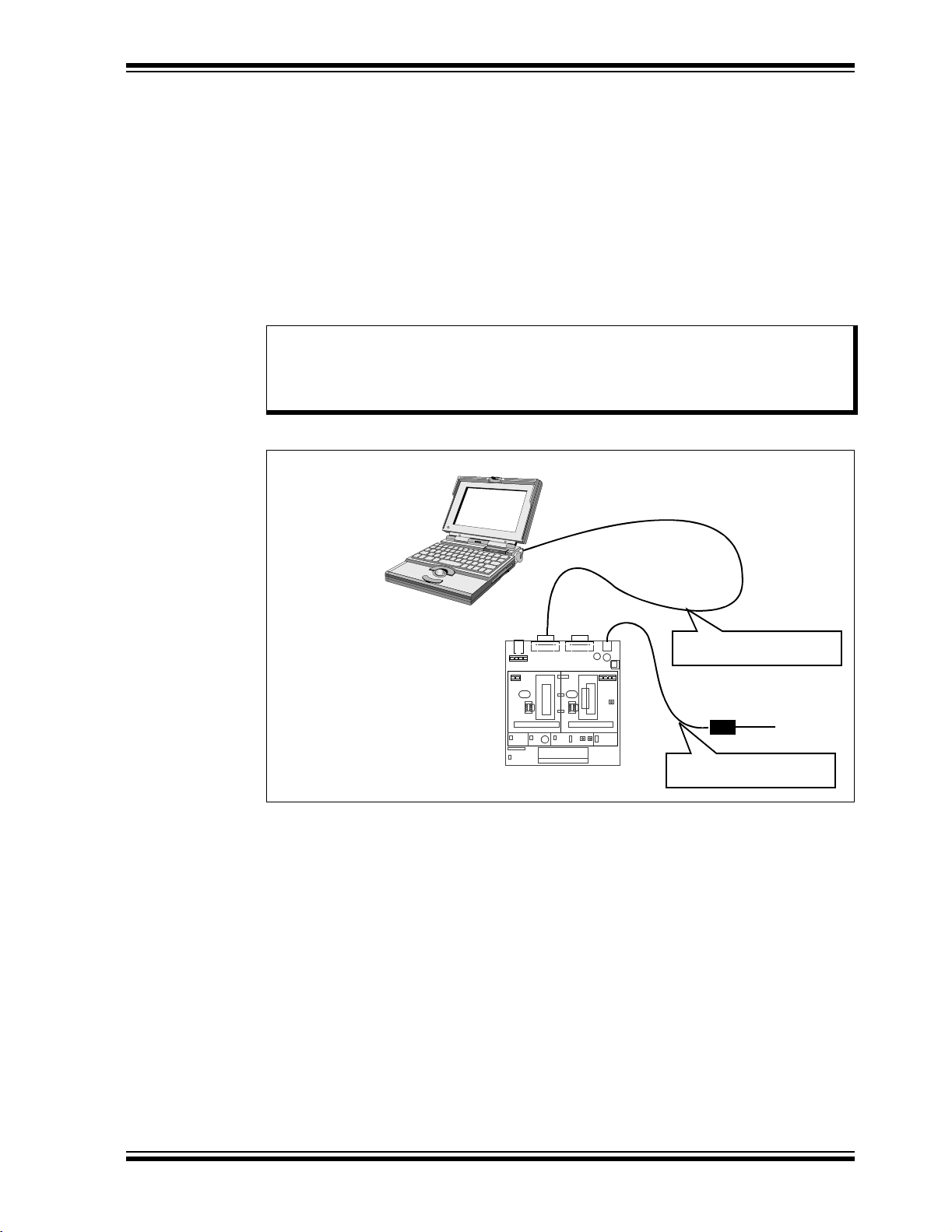
2.4.2 Connect PC and Start HyperTerminal Session
Follow the information in Figure 2-2 to set up your PC to operate with the dsPICDEM™
2 Development Board.
1. Use an RS-232 cable to connect the serial port on your PC to the UART connector (J2) on the board.
2. On your PC, start a HyperTerminal session and set it up with these port settings:
9600 baud
8 data bits
No parity
1 stop bit
No flow control
Note: For convenience, each of the sample program folders contains a utility that
automatically launches HyperTerminal set up to run with the demo program. Double clicking the file (Hyperterminal_RS232_dsPICDEM2.ht)
starts the session.
FIGURE 2-2: SETUP DIAGRAM
PC running HyperTerminal
®
dsPICDEM™ 2 Development Board
running sample application
J1 J2
UART
J2
1234
GP 40
GP 28
GP 18
M ALL
12
Motor
Control
H8 H9
CAN
J3
U2A1 U1A1
U2B1
General
Purpose
J4
Connect RS-232 cable to
PC
1234
U1B1
U1C1
9 VDC Power Cable
115 VAC
Apply power to the board
© 2005 Microchip Technology Inc. DS51558A-page 15
Page 22
dsPICDEM 2 Development Board User’s Guide
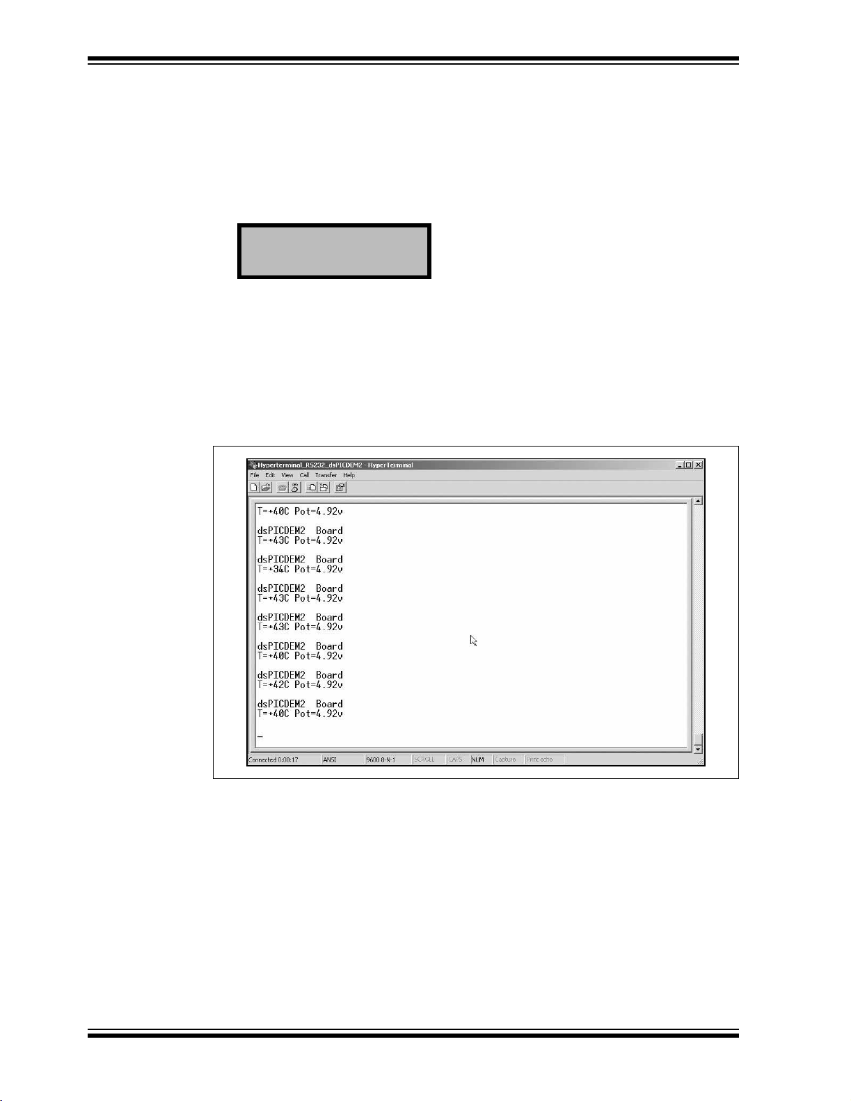
2.4.3 Observe Sample Application
To run and observe the sample application follow these steps:
1. Plug the 9 VDC cable into the DC IN connector (J4). The PWR ON indicator
should illuminate.
2. Press the RESET ALL pushbutton (S1). The LCD displays the current tempera-
ture and voltage values, which represent the A/D conversions from the temperature sensor and potentiometer, respectively.
dsPICDEM™ 2 Board
T=+18C Pot=3.42v
The LED indicators (D3 and D4) should initially be off and then start to blink.
3. Touch the temperature sensor for a moment and observe the temperature reading. It should increase as your finger warms the sensor.
4. Adjust the potentiometer clockwise and observe the voltage reading increase.
Then readjust it counterclockwise and observe the voltage reading decrease.
5. Observe the HyperTerminal screen and note that the information is updated to
match the LCD (see Figure 2-3).
FIGURE 2-3: TYPICAL HyperTerminal
6. Press pushbutton S5 (INT0) once and note that the rate at which D3 and D4 blink
changes. As you press S5 again, observe that the blink rate cycles from
extremely fast (both LEDs appear to be on) to fast (blinking rapidly) to moderate
(blinking slowly) to slow (appear to be switching on and off).
7. Press pushbutton S6 (INT1) once and note that D3 and D4 blink alternately. As
you press S6 again, note the LEDs cycle between blinking together and blinking
alternately.
®
SESSION
DS51558A-page 16 © 2005 Microchip Technology Inc.
Page 23
2.5 DEVICE PROGRAMMING PROCESS
The second phase of the getting-started process introduces the MPLAB Integrated
Development Environment (IDE) and MPLAB ICD 2 In-Circuit Debugger. The
emphasis in this phase is to program the sample application into a dsPIC30F4011
device. After observing the demonstration, this process gets you ready to examine
what you observed.
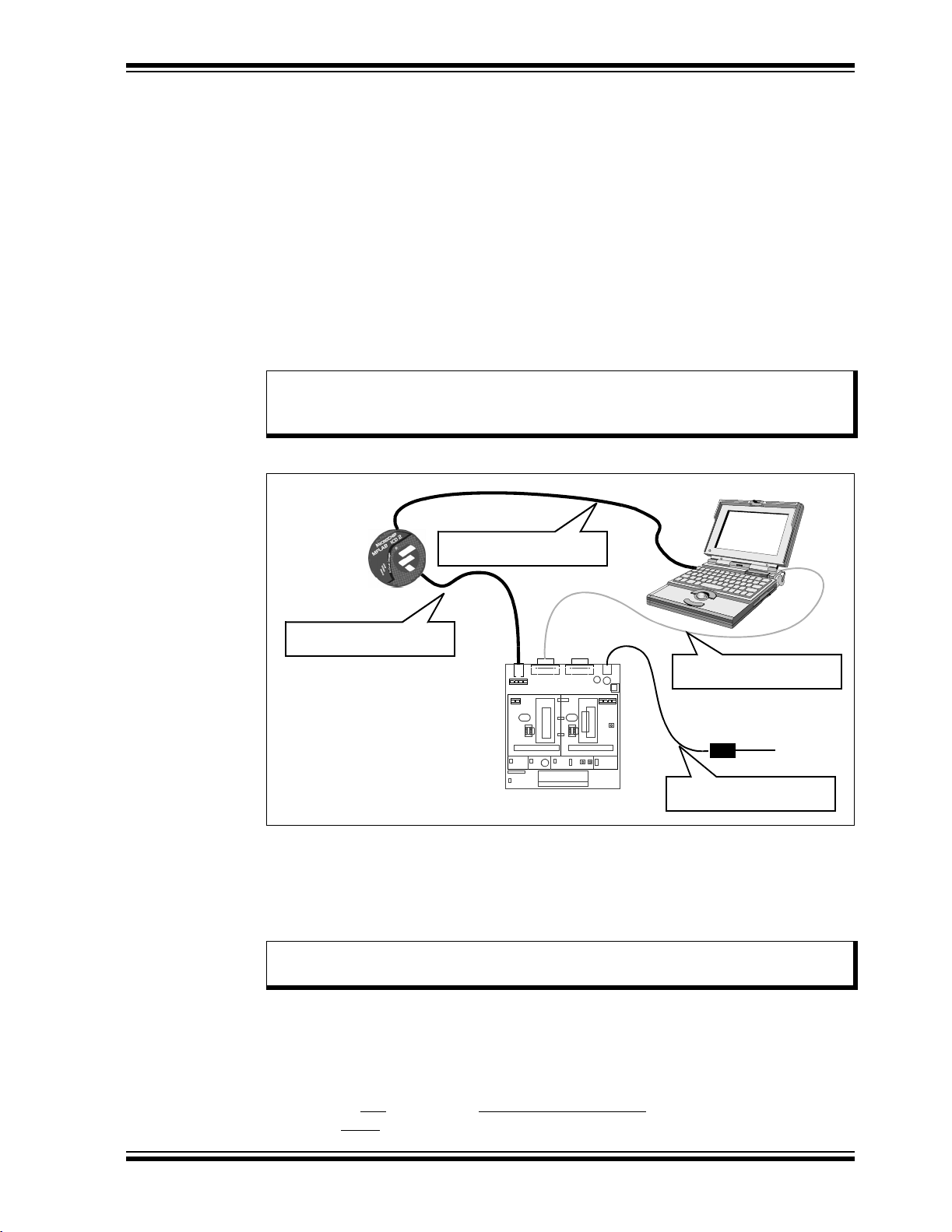
2.5.1 Connect MPLAB ICD 2
Follow the information in Figure 2-2 to set up the MPLAB ICD 2 for use as a
programmer.
1. With an RJ11 cable, connect the MPLAB ICD 2 to the ICD header (J1) on the
board.
2. Use a USB cable to connect the MPLAB ICD 2 to your PC.
Note: Make sure that the USB driver for the MPLAB ICD 2 has been installed on
your PC (see the
regarding the installation of MPLAB ICD 2).
MPLAB® ICD 2 User’s Guide
Getting Started
, DS51331, for more details
FIGURE 2-4: MPLAB
®
ICD 2 CONNECTION DIAGRAM
PC running MPLAB
®
IDE
MPLAB ICD 2
Connect USB cable to PC
Connect RJ-11 cable to ICD
dsPICDEM™ 2 Development Board
running dsPIC30F4011 sample
J1 J2
UART
J2
1234
GP 40
GP 28
GP 18
M ALL
12
Motor
Control
H8 H9
U2A1 U1A1
U2B1
J4
CAN
J3
1234
U1B1
General
Purpose
U1C1
Connect RS-232 cable to
PC
9 VDC Power Cable
115 VAC
application
Apply power to the board
2.5.2 Setting up MPLAB IDE
The sample application program files on the dsPICDEM 2 CD contain a workspace and
project information needed by MPLAB IDE, MPLAB ICD 2 and MPLAB C30.
The first step is to open the sample application project in MPLAB IDE.
Note: These instructions presume the use of MPLAB IDE version 7.11 or newer
and MPLAB C30 version 1.32 or newer.
A project contains the files needed to build an application (source code, linker script
files, etc.) along with their associations to various build tools and build options. A workspace contains information on the selected device, debug tool and/or programmer,
open windows and their location, and other MPLAB IDE configuration settings.
1. Start MPLAB IDE.
2. From the
where
© 2005 Microchip Technology Inc. DS51558A-page 17
File
menu select
[path]
is the location of the sample application files.
Open Workspace>[path],
as shown in Figure 2-5,
Page 24
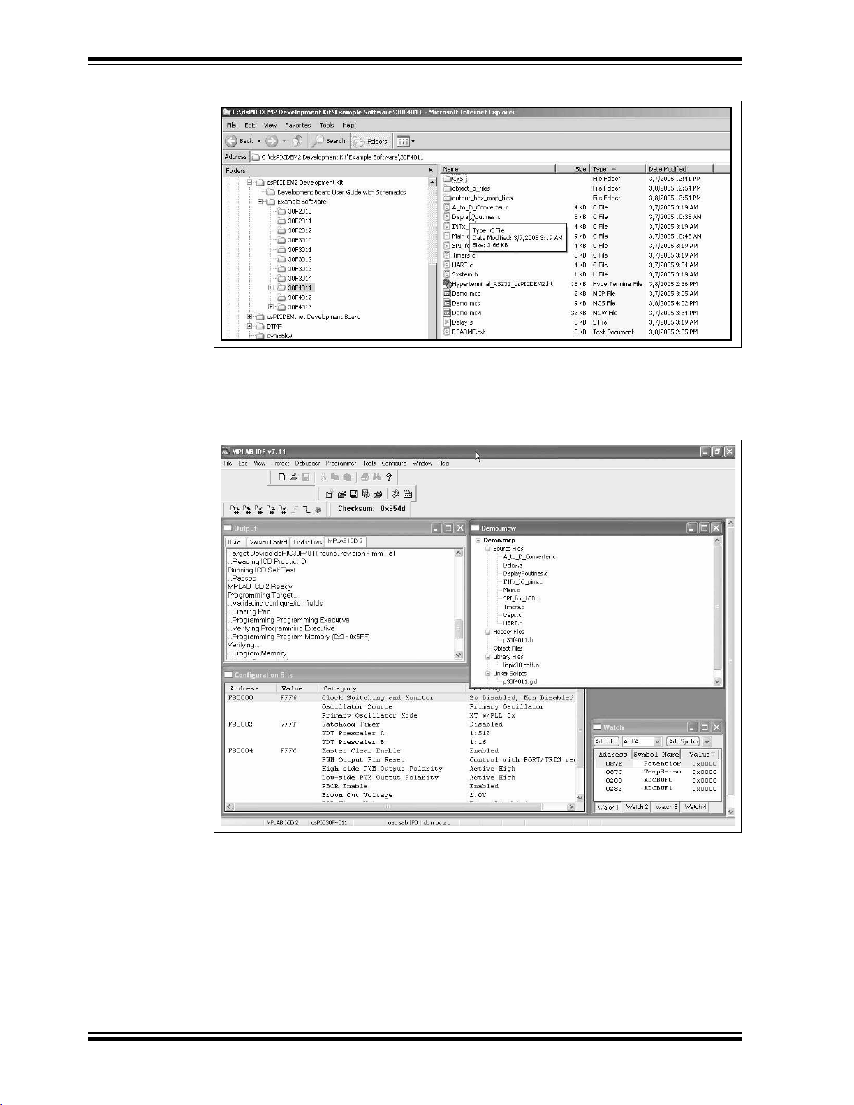
dsPICDEM 2 Development Board User’s Guide
FIGURE 2-5: OPEN WORKSPACE DIALOG
3. Select 30F4011/Demo.mcw. A project and workspace is created in MPLAB IDE.
As shown in Figure 2-6, Demo.mcw is the workspace file and Demo.mcp is the
project file.
FIGURE 2-6: PROJECT WORKSPACE IN MPLAB
®
IDE
DS51558A-page 18 © 2005 Microchip Technology Inc.
Page 25

2.5.3 Build the Project
Getting Started
1. Select
2. Observe the progress of the build in the Output window.
3. When BUILD SUCCEEDED displays you are ready to program the device.
4. Program the dsPIC30F4011device (
Project>Build All
.
2.5.4 Run the Application
1. From the
exectution
2. On the board, turn off the M ALL switch in S2.
3. As the code begins executing, note that the operation is identical to what you
observed out-of-the-box (see Section 2.4.3 “Observe Sample Application”)
Programmer
.
menu, select
2.6 IN-CIRCUIT DEBUGGING PROCESS
MPLAB IDE lets you run, halt and step the program. It lets you set breakpoints to
examine the code at specific locations or on occurrence of specific events. It also lets
you examine the contents of the RAM and registers. The MPLAB ICD 2 allows you to
run the application on the dsPICDEM 2 while monitoring it in MPLAB IDE on your PC.
The examination process requires that three changes be made to the sample
application setup.
• The dsPIC30F4011 device must be reprogrammed to recognize the MPLAB ICD
2 as a debugger rather than as a programmer.
• MPLAB IDE must be reconfigured to specify the pins on the dsPIC30F device to
be used for debugging.
• The dsPICDEM 2 board must be physically reconfigured to ensure that it connects
the MPLAB ICD 2 debugger to the pins on the dsPIC30F device that were
specified in MPLAB IDE.
Programmer>Program
Release from Reset to
)
enable code
Note: The primary programming and debugging functions (PGC/EMUC,
PGD/EMUD) on the dsPIC30F device are multiplexed with other peripheral
modules on the device used by the sample application. Thus it is necessary
to use an alternate pair of debugging pins (EMUC1/EMUD1,
EMUC2/EMUD2 or EMUC3/EMUD3) to examine the baseline code
provided in the sample application.
2.6.1 Select MPLAB ICD 2 as Debugger
To change MPLAB ICD 2 from a programmer to a debugger for a dsPIC30F4011
device:
1. From the
MPLAB ICD 2 as the debug tool in MPLAB IDE.
2. From the
window displays the current configuration settings for the device, as shown in
Figure 2-7.
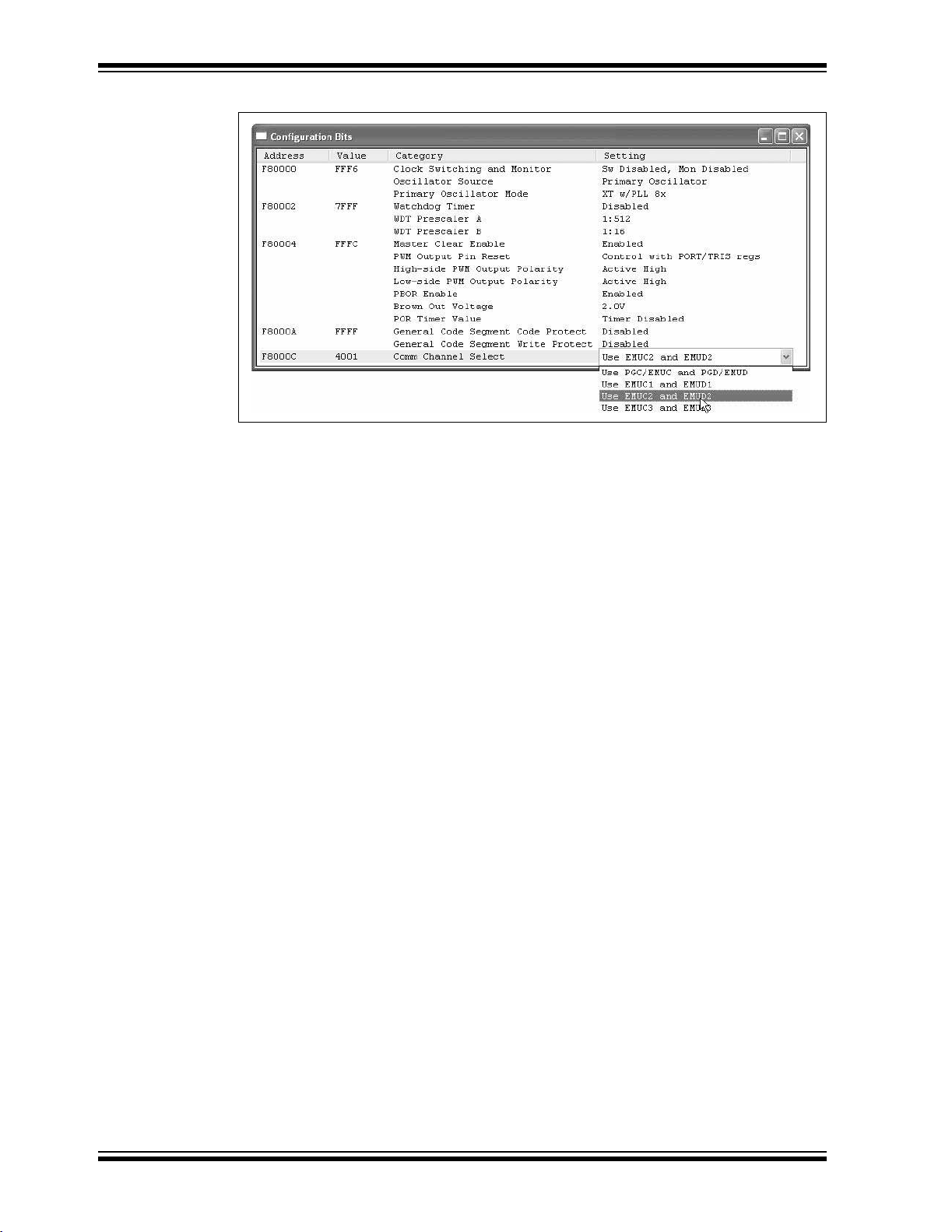
3. Change the “Comm Channel Select” parameter to Use EMUC2 and EMUD2.
4. On the dsPICDEM 2 board, change the setting on switch S3 to turn on EMUC2
and EMUD2.
5. Program the dsPIC30F device (
6. On the dsPICDEM 2 board, turn off M ALL on switch S2.
7. Reset the program and run it. From the
Reset
Debugger
Configure
. Then select
menu, click
menu, select
Select Tool>MPLAB ICD 2
Debugger>Program
Debugger>Run
Configuration Bits...
Debugger
.
menu, select
to designate the
The Configuration Bits
menu).
Reset>Processor
© 2005 Microchip Technology Inc. DS51558A-page 19
Page 26
dsPICDEM 2 Development Board User’s Guide
FIGURE 2-7: CONFIGURATION BITS WINDOW
2.6.2 Debugging the Code
The MPLAB ICD 2 In-Circuit Debugger can be used to run, halt and step the code. A
breakpoint can be set to halt the program after the code has executed the instruction
at the breakpoint. The contents of the RAM and registers can be viewed whenever the
processor has been halted.
The MPLAB ICD 2 In-Circuit Debugger uses the following function keys to access the
main debugging functions:
<F5> Halt
<F6> Reset
<F7> Single Step
<F9> Run
In addition, there are more functions available by right clicking on a line of source code.
These functions include the ability to set simple and advanced breakpoints.
2.7 SUMMARY
This chapter has provided a suggested process for using the dsPICDEM™ 2
Development Board to jump start your own application. If you have reviewed this
process, you should be able to:
• Configure the dsPICDEM™ 2 Development Board for the dsPIC30F device you
select for your application.
• Set up MPLAB IDE to use the MPLAB ICD 2 In-Circuit Debugger.
• Locate the sample application for your dsPIC30F device.
• Program the chip with the MPLAB ICD 2.
• View the code execution in program memory and source code.
• Reset, Run, Halt and Single-Step the code.
DS51558A-page 20 © 2005 Microchip Technology Inc.
Page 27
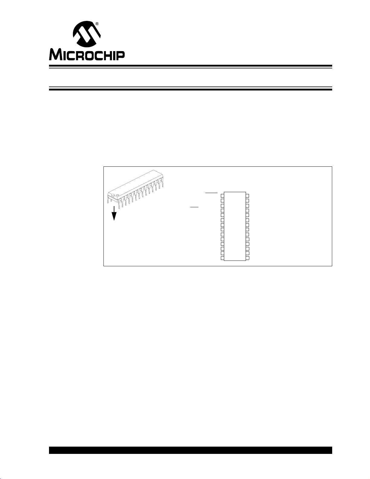
Chapter 3. Using the dsPIC30F2010
3.1 INTRODUCTION
This chapter assumes you have chosen the dsPIC30F2010 for your application. The
dsPICDEM 2 Development Board supports a dsPIC30F2010 device in a 28-pin SPDIP
package, as shown in Figure 3-1. This device provides six 10-bit A/D (500 ksps)
channels, a UART, an SPI module, an I
application program provides a software baseline for building your own embedded
solution.
FIGURE 3-1: 28-PIN SPDIP dsPIC30F2010
dsPICDEM™ 2
DEVELOPMENT BOARD
USER’S GUIDE
2
C™ module and 20 I/O pins. A sample
U2B1
EMUD3/AN0/VREF+/CN2/RB0
EMUC3/AN1/V
EMUD1/SOSCI/T2CK/U1ATX/CN1//RC13
EMUC1/SOSCO/T1CK/U1ARX/CN0/RC14
AN2/SS1/CN4/RB2
AN3/INDX/CN5/RB3
AN4/QEA/IC7/CN6/RB4
AN5/QEB/IC8/CN7/RB5
OSC2/CLKO/RC15
EMUD2/OC2/IC2/INT2/RD1
MCLR
REF-/CN3/RB1
OSC1/CLKI V
VDD
1
28
AV
DD
2
3
4
5
6
7
SS
8
9
10
11
12
13
14
AVSS
27
PWM1L/RE0
26
PWM1H/RE1
25
PWM2L/RE2
24
PWM2H/RE3
23
PWM3L/RE4
22
PWM3H/RE5V
21
DD
20
V
SS
19
dsPIC30F2010
PGC/EMUC/U1RX/SDI1/SDA/RF2
18
PGD/EMUD/U1TX/SDO1/SCL/RF3
17
FLTA/INT0/SCK1/OCFA/RE8
16
15
EMUC2/OC1/IC1/INT1/RD0
3.2 HIGHLIGHTS
This chapter discusses:
• Board Setup for the dsPIC30F2010 Sample Application
• Device Programming
• Observing the Sample Application
• In-Circuit Debugging
• Summary
3.3 BOARD SETUP FOR THE dsPIC30F2010 SAMPLE APPLICATION
The dsPICDEM 2 Development Board supports dsPIC30F devices that have multiple
peripheral devices multiplexed on some pins. Therefore, the jumper set up of various
headers depends on which of the dsPIC30F peripherals are used by the application.
This section demonstrates how the board is set up for the dsPIC30F2010 device to
support the dsPIC30F2010 example software in the dsPICDEM 2 Development Kit CD.
Follow these steps to configure the hardware on the dsPICDEM 2 Development Board
for the sample application.
1. Disconnect the power source.
2. Remove any dsPIC30Fxxxx device currently plugged into the dsPICDEM 2
Development Board.
© 2005 Microchip Technology Inc. DS51558A-page 21
Page 28

dsPICDEM 2 Development Board User’s Guide
3. Plug the dsPIC30F2010 into socket U2B1.
4. Configure the hardware components as shown in Table 3-1.
TABLE 3-1: dsPIC30F2010 CONFIGURATION SETTINGS
Header Socket U2B1
Component
Jumper JP1 JP1 Jumper — 5 VDC jumper installed
Jumper JP2 JP2 Jumper — 5 VDC jumper installed
Selector Switch S2 M ALL ON 17,18 PGC and PGD
Selector Switch S3 OFF — Not used in this configuration
Selector Switch S4 OFF — Not used in this configuration
PGM U3 H11 Open — —
CAN Tx H2 Open — —
CAN Rx H2 Open — —
UART1 Tx* H3 Open — —
UART1 Rx* H3 Open — —
Alternate UART1 Tx*H4 M ALL 11 EMUD1/SOSCI/T2CK/U1ATX/CN1/RC13
Alternate UART1 Rx*
UART2 Tx* H5 Open — —
UART2 Rx* H5 Open — —
Temperature Sensor H10 M ALL 5 AN3/INDX/CN5/RB3
Potentiometer H13 M ALL 4 AN2/SS1
Switch S5 H6 M ALL 16 FLTA/INT0/SCK1/OCFA/RE8
Switch S6 H7 M ALL 15 EMUC2/OC1/IC1/INT1/RD0
LED D3 H12 M D3 2 EMUD3/AN0/V
LED D4 H12 M D4 3 EMUC3/AN1/V
LCD - SPI™ Clock
LCD - SPI Data
* On this device, multiplexing of various peripherals on the pins does not allow the
*
simultaneous use of:
– Switch S5 and LCD
– Primary UART1 pins and LCD.
Since only one DB-9 connector is provided for RS-232 communication, you can
select either UART1 (primary or alternate pins) or UART2, but not both.
No.
H4 M ALL 12 EMUC1/SOSCO/T1CK/U1ARX/CN0/RC14
*
H1 M28 16 FLTA/INT0/SCK1/OCFA/RE8
H1 M28 17 PGD/EMUD/U1TX/SDO1/SCL/RF3
Jumper
Setting
Pin Device Functions (see Figure 3-1)
/CN4/RB2
REF+/CN2/RB0
REF-/CN3/RB1
5. Connect the RS-232 cable from the PC to the UART connector (J2).
6. Reapply power to the DC IN connector (J4). The PWR ON LED should illuminate.
7. Load the sample application program for the dsPIC30F2010 (see
Section 3.4 “Device Programming”).
DS51558A-page 22 © 2005 Microchip Technology Inc.
Page 29
3.4 DEVICE PROGRAMMING
Load the sample application program for the dsPIC30F2010 using this process:
1. Plug the RJ11cable from the MPLAB ICD 2 into the ICD header (J1). Make sure
the USB cable from the MPLAB ICD 2 is connected to your PC.
2. Start MPLAB IDE.
3. Open the dsPIC30F2010 sample project (
path/dsPICDEM 2 Development Kit/Example Software/30F2010/Demo.mcw
Note: For detailed information and procedures on using the MPLAB IDE and ICD
2 refer to Chapter 2 “Getting Started”.
Using the dsPIC30F2010
File>Open Workspace)
.
from
4. Build the sample project in MPLAB IDE (
5. On the dsPICDEM™ 2 board set all positions on switches S3 and S4 to OFF.
Then set switch S2 to M ALL. The MPLAB ICD 2 is now connected to the PGC
and PGD pins on the dsPIC30F2010.
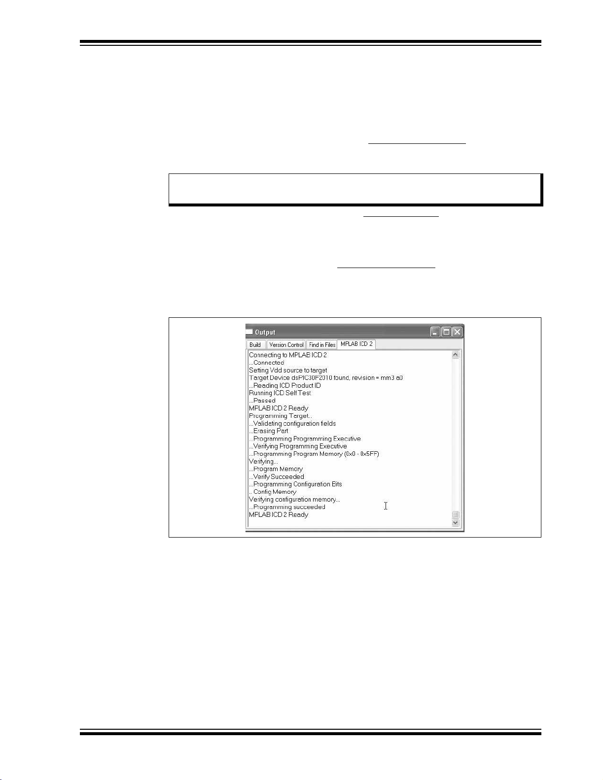
6. Download the sample application (
(Figure 3-2) displays the status as the download occurs and indicates when the
programming has succeeded.
FIGURE 3-2: PROGRAMMING THE dsPIC30F2010 DEVICE
Project>Build All)
Programmer>Program
.
). The Output window
7. Disconnect the MPLAB ICD 2 cable from the ICD header. The program is now
ready to run (see Section 3.5 “Observing the Sample Application”).
© 2005 Microchip Technology Inc. DS51558A-page 23
Page 30

dsPICDEM 2 Development Board User’s Guide
3.5 OBSERVING THE SAMPLE APPLICATION
1. Press RESET ALL. The program begins to run.
2. Set up a HyperTerminal session on the PC to run with these parameters:
Port Setting Value
Bits per second 9600
Data bits 8
Parity None
Stop bits 1
Flow control None
As a shortcut, you can launch the Hyperterminal_RS232_dsPICDEM2.ht
file in the dsPICDEM 2 Development Kit/Example Software/30F2010
folder.
3. See information on LCD. Note that the HyperTerminal displays the same
information.
4. Adjust temperature and note LCD and HyperTerminal readings.
5. Adjust potentiometer and note LCD and HyperTerminal readings.
6. Observe the rate at which LEDs D3 and D4 blink.
7. Press S6 (INT1) and note the affect on D3 and D4.
DS51558A-page 24 © 2005 Microchip Technology Inc.
Page 31

3.6 IN-CIRCUIT DEBUGGING
The sample application program is intended to illustrate how the processor and
peripheral modules handle the functionality provided on the dsPICDEM 2 Development
Board. The MPLAB ICD 2 In-Circuit Debugger was used to program the sample
application into the dsPIC30F device. You can also use the MPLAB ICD 2 In-Circuit
Debugger to examine this baseline code to determine specific applicability to your
application.
The examination process requires that three changes be made to the sample
application setup.
• The dsPIC30F2010 device must be reprogrammed to recognize the MPLAB ICD
2 as a debugger rather than as a programmer.
• MPLAB IDE must be reconfigured to specify the pins on the dsPIC30F2010
device to be used for debugging.
• The dsPICDEM 2 board must be physically reconfigured to ensure that it connects
the MPLAB ICD 2 debugger to the pins on the dsPIC30F2010 device that were
specified in MPLAB IDE.
The primary programming and debugging functions (PGC/EMUC, PGD/EMUD) on the
dsPIC30F device are multiplexed with other peripheral modules on the device used by
the sample application. Thus it is necessary to use an alternate pair of debugging pins
(EMUC1/EMUD1, EMUC2/EMUD2 or EMUC3/EMUD3) to examine the baseline code
provided in the sample application.
Using the dsPIC30F2010
3.6.1 Setting Up MPLAB ICD 2 for Debugging
To change MPLAB ICD 2 from a programmer to a debugger:
1. From the
MPLAB ICD 2 as the debug tool in MPLAB IDE.
2. From the
window displays the current configuration settings for the device, as shown in
Figure 3-3.
3. Change the “Comm Channel Select” parameter to Use EMUC2 and EMUD2.
4. On the dsPICDEM 2 board, change the setting on switch S3 to turn on EMUC2
and EMUD2.
5. Remove any jumpers on headers H6 and H7.
6. Reprogram the dsPIC30F device (
7. On the dsPICDEM 2 board, turn off M ALL on switch S2.
8. Reset the program and run it. From the
Reset
Debugger
Configure
. Then select
menu, click
menu, select
Select Tool>MPLAB ICD 2
Debugger>Run
Configuration Bits...
Debugger>Program
Debugger
.
menu, select
to designate the
The Configuration Bits
menu).
Reset>Processor
© 2005 Microchip Technology Inc. DS51558A-page 25
Page 32

dsPICDEM 2 Development Board User’s Guide
FIGURE 3-3: CONFIGURATION BITS WINDOW
3.6.2 Examining the Code
After the application has been reprogrammed to use the MPLAB ICD 2 as a debugger,
you can use MPLAB IDE to run, halt and step the program. You can set breakpoints to
halt the program and examine the actual code at any point. You can also examine the
contents of the RAM and registers whenever the processor is halted.
Refer to Section 2.3 “Getting Started” for an overview of the sample application.
Flowcharts illustrate each of these processes:
• Startup and initialization
• Main loop processing
• A/D conversion processing
• External interrupt processing
The dsPICDEM 2 Development Kit/Example Software/30F2010 folder
contains fully annotated code files that you can examine, compare and copy.
3.7 SUMMARY
This chapter has provided specific instructions for using the dsPICDEM 2 Development
Board with a dsPIC30F2010 device. If you have reviewed this process, you should be
able to:
• Configure the dsPICDEM 2 Development Board for the dsPIC30F2010 device.
• Set up MPLAB IDE to use the MPLAB ICD 2 In-Circuit Debugger.
• Locate the sample application for the dsPIC30F2010 device.
• Program the chip with the MPLAB ICD 2.
• Examine the sample application and identify applicable code for your embedded
solution.
DS51558A-page 26 © 2005 Microchip Technology Inc.
Page 33

Chapter 4. Using the dsPIC30F201 1
4.1 INTRODUCTION
This chapter assumes you have chosen the dsPIC30F2011 for your application. The
dsPICDEM 2 Development Board supports a dsPIC30F2011 device in an 18-pin PDIP
package, as shown in Figure 4-1. This device provides eight 12-bit A/D (100 ksps)
channels, a UART, an SPI module, an I
tion program provides a software baseline for building your own embedded solution.
FIGURE 4-1: 18-PIN PDIP dsPIC30F2011
dsPICDEM™ 2
DEVELOPMENT BOARD
USER’S GUIDE
2
C module and 12 I/O pins. A sample applica-
EMUD3\AN0/V
EMUD3\AN1/VREF-/CN3/RB1
AN2/SS1
U1A1
EMUD1/SOSCI/T2CK/U1ATX/CN1/RC13
EMUC1/SOSCO/T1CK/U1ARX/CN0/RC14
REF+/CN2/RB0
/LVDIN/CN4/RB2
AN3/CN5/RB3
OSC2/CLKO/RC15
MCLR
OSC1/CLKI
1
2
3
4
5
6
7
8
9
18
DD
AV
17
AV
SS
16
AN6/SCK1/INT0/OCFA/RB6
15
EMUD2/AN7/OC2/IC2/INT2/RB7
14
DD
V
V
SS
13
PGC/EMUC/AN5/U1RX/SDI1/SDA/CN7/RB5
12
11
PGD/EMUD/AN4/U1TX/SDO1/SCL/CN6/RB4
EMUC2/OC1/IC1/INT1/RD0
10
dsPIC30F2011
4.2 HIGHLIGHTS
This chapter discusses:
• Board Setup for the dsPIC30F2011 Sample Application
• Device Programming
• Observing the Sample Application
• In-Circuit debugging
• Summary
4.3 BOARD SETUP FOR THE dsPIC30F2011 SAMPLE APPLICATION
The dsPICDEM 2 Development Board supports dsPIC30F devices that have multiple
peripheral devices multiplexed on some pins. Therefore, the jumper set up of various
headers depends on which of the dsPIC30F peripherals are used by the application.
This section demonstrates how the board is set up for the dsPIC30F2011 device to
support the dsPIC30F2011 example software in the dsPICDEM 2 Development Kit CD.
Follow these steps to configure the hardware on the dsPICDEM 2 Development Board
for the sample application.
1. Disconnect the power source.
2. Remove any dsPIC30Fxxxx device currently plugged into the dsPICDEM 2
Development Board.
3. Plug the dsPIC30F2011 into socket U1C1.
© 2005 Microchip Technology Inc. DS51558A-page 27
Page 34

dsPICDEM 2 Development Board User’s Guide
4. Configure the hardware components as shown in Table 4-1.
TABLE 4-1: dsPIC30F2011 CONFIGURATION SETTINGS
Header Socket U1A1
Component
Jumper JP1 JP1 Jumper — 5 VDC jumper installed
Jumper JP2 JP2 Jumper — 5 VDC jumper installed
Selector Switch S2 GP 18 ON 11,12 PGC and PGD
Selector Switch S3 OFF — Not used in this configuration
Selector Switch S4 OFF — Not used in this configuration
PGM U3 H11 Open — No jumper connections
CAN Tx H2 Open — —
CAN Rx H2 Open — —
UART1 Tx* H3 Open — —
UART1 Rx* H3 Open — —
Alternate UART1 Tx
Alternate UART1 Rx *H4 GP ALL 9 EMUC1/SOSCO/T1CK/U1ARX/CN0/RC14
UART2 Tx* H5 Open — —
UART2 Rx* H5 Open — —
Temperature Sensor H10 GP ALL 5 AN3/CN5/RB3
Potentiometer H13 GP ALL 4 AN2/SS1
Switch S5 H6 Open — —
Switch S6 H7 GP 18 10 EMUC2/OC1/IC1/INT1/RD0
LED D3 H12 GP D3 2 AN0/V
LED D4 H12 GP D4 3 AN1/V
LCD - SPI™ Clock* H1 GP 18 16 AN6/SCK1/INT0/OCFA/RB6
LCD - SPI Data* H1 GP18 11
* On this device, multiplexing of various peripherals on the pins does not allow the
simultaneous use of:
– Switch S5 and LCD
– Primary UART1 pins and LCD.
Since only one DB-9 connector is provided for RS-232 communication, you can
select either UART1 (primary or alternate pins) or UART2, but not both.
No.
* H4 GP ALL 8 EMUD1/SOSC1/T2CK/U1ATX/CN1/RC13
Jumper
Setting
Pin Device Functions (see Figure 4-1)
/LVDIN/CN4/RB2
REF+/CN2/RB0
REF-/CN3/RB1
PGD/EMUD/AN4/U1TX/SDO1/SCL/CN6/RB4
5. Connect the RS-232 cable from the PC to the UART connector (J2).
6. Reapply power to the DC IN connector (J4). The PWR ON LED should illuminate.
7. Load the sample application program for the dsPIC30F2011 (see
Section 4.4 “Device Programming”).
DS51558A-page 28 © 2005 Microchip Technology Inc.
Page 35

4.4 DEVICE PROGRAMMING
Load the sample application program for the dsPIC30F2011 using this process:
1. Plug the RJ11 (telephone) cable from the MPLAB ICD 2 into the ICD header (J1).
Make sure the USB cable from the MPLAB ICD 2 is connected to your PC.
2. Start MPLAB IDE.
3. Open the dsPIC30F2011 sample project (
path/dsPICDEM 2 Development Kit/Example Software/30F2011/Demo.mcw.
Note: For detailed information and procedures on using the MPLAB IDE and ICD
2, refer to Chapter 2 “Getting Started”.
Using the dsPIC30F2011
File>Open Workspace)
from
4. Build the sample project in MPLAB IDE (
5. On the dsPICDEM™ 2 board set all positions on switches S3 and S4 to off. Then
set switch S2 to GP 18. The MPLAB ICD 2 is now connected to the PGC and
PGD pins on the dsPIC30F2011.
6. Download the sample application (
(Figure 4-2) displays the status as the download occurs and indicates when the
programming has succeeded.
FIGURE 4-2: PROGRAMMING THE dsPIC30F2011 DEVICE
Project>Build All)
Programmer>Program
.
). The Output window
7. Disconnect the MPLAB ICD 2 cable from the ICD header. The program is now
ready to run (see Section 4.5 “Observing the Sample Application”).
© 2005 Microchip Technology Inc. DS51558A-page 29
Page 36

dsPICDEM 2 Development Board User’s Guide
4.5 OBSERVING THE SAMPLE APPLICATION
1. Press RESET ALL. The program begins to run.
2. Set up a HyperTerminal session on the PC to run with these parameters:
Port Setting Value
Bits per second 9600
Data bits 8
Parity None
Stop bits 1
Flow control None
As a shortcut, you can launch the Hyperterminal_RS232_dsPICDEM2.ht
file in the dsPICDEM 2 Development Kit/Example Software/30F2011
folder.
3. See information on LCD. Note that the HyperTerminal displays the same
information.
4. Adjust temperature and note LCD and HyperTerminal readings.
5. Adjust potentiometer and note LCD and HyperTerminal readings.
6. Observe the rate at which LEDs D3 and D4 blink.
7. Press S6 (INT1) and note the affect on D3 and D4.
DS51558A-page 30 © 2005 Microchip Technology Inc.
Page 37

4.6 IN-CIRCUIT DEBUGGING
The sample application program is intended to illustrate how the processor and I/O
modules handle the functionality provided on the dsPICDEM 2 Development Board.
The MPLAB ICD 2 In-Circuit Debugger was used to program the sample application
into the dsPIC30F device. You can also use the MPLAB ICD 2 In-Circuit Debugger to
examine this baseline code to determine specific applicability to your application.
The examination process requires that three changes be made to the sample application setup.
• The dsPIC30F2011 device must be reprogrammed to recognize the MPLAB ICD
2 as a debugger rather than as a programmer.
• MPLAB IDE must be reconfigured to specify the pins on the dsPIC30F2011
device to be used for debugging.
• The dsPICDEM 2 board must be physically reconfigured to ensure that it connects
the MPLAB ICD 2 debugger to the pins on the dsPIC30F2011 device that were
specified in MPLAB IDE.
The primary programming and debugging functions (PGC/EMUC, PGD/EMUD) on the
dsPIC30F device are multiplexed with other peripheral modules on the device used by
the sample application. Thus it is necessary to use an alternate pair of debugging pins
(EMUC1/EMUD1, EMUC2/EMUD2 or EMUC3/EMUD3) to examine the baseline code
provided in the sample application.
Using the dsPIC30F2011
4.6.1 Setting Up MPLAB ICD 2 for Debugging
To change MPLAB ICD 2 from a programmer to a debugger:
1. From the
MPLAB ICD 2 as the debug tool in MPLAB IDE.
2. From the
window displays the current configuration settings for the device, as shown in
Figure 4-3.
3. Change the “Comm Channel Select” parameter to Use EMUC2 and EMUD2.
4. On the dsPICDEM 2 board, change the setting on switch S4 to turn on EMUC2
and EMUD2 for GP 18.
5. Remove any jumpers on headers H6 and H7.
6. Reprogram the dsPIC30F device (
7. On the dsPICDEM 2 board, turn off GP 18 on switch S2.
8. Reset the program and run it. From the
Reset
Debugger
Configure
. Then select
menu, click
menu, select
Select Tool>MPLAB ICD 2
Debugger>Run
Configuration Bits...
Debugger>Program
Debugger
.
menu, select
to designate the
The Configuration Bits
menu).
Reset>Processor
© 2005 Microchip Technology Inc. DS51558A-page 31
Page 38

dsPICDEM 2 Development Board User’s Guide
FIGURE 4-3: CONFIGURATION BITS WINDOW
4.6.2 Examining the Code
After the application has been reprogrammed to use the MPLAB ICD 2 as a debugger,
you can use MPLAB IDE to run, halt and step the program. You can set breakpoints to
halt the program and examine the actual code at any point. You can also examine the
contents of the RAM and registers whenever the processor is halted.
Refer to Section 2.3 “Getting Started” for an overview of the sample application.
Flowcharts illustrate each of these processes:
• Startup and initialization
• Main loop processing
• A/D conversion processing
• External interrupt processing
The dsPICDEM 2 Development Kit/Example Software/30F2011 folder
contains fully annotated code files that you can examine, compare and copy.
4.7 SUMMARY
This chapter has provided specific instructions for using the dsPICDEM 2 Development
Board with a dsPIC30F2011 device. If you have reviewed this process, you should be
able to:
• Configure the dsPICDEM 2 Development Board for the dsPIC30F2011 device.
• Set up MPLAB IDE to use the MPLAB ICD 2 In-Circuit Debugger.
• Locate the sample application for the dsPIC30F2011 device.
• Program the chip with the MPLAB ICD 2.
• Examine the sample application and identify applicable code for your embedded
solution.
DS51558A-page 32 © 2005 Microchip Technology Inc.
Page 39

Chapter 5. Using the dsPIC30F2012
5.1 INTRODUCTION
This chapter assumes you have chosen the dsPIC30F2012 for your application. The
dsPICDEM 2 Development Board supports a dsPIC30F2012 device in an 28-pin,
SPDIP package, as shown in Figure 5-1. This device provides ten 12-bit A/D (100 ksps)
channels, a UART, an SPI module, an I
tion program provides a software baseline for building your own embedded solution.
FIGURE 5-1: 28-PIN SPDIP dsPIC30F2012
dsPICDEM™ 2
DEVELOPMENT BOARD
USER’S GUIDE
2
C module and 20 I/O pins. A sample applica-
AV
DD
28
AVSS
27
AN6/OCFA/RB6
26
EMUD2/AN7/RB7
25
AN8/OC1/RB8
24
AN9/OC2/RB9
23
CN17/RF4
22
CN18/RF5
21
DD
20
SSOSC2/CLKO/RC15
V
19
PGC/EMUC/U1RX/SDI1/SDA/RF2
18
PGD/EMUD/U1TX/SDO1/SCL/RF3
17
SCK1/INT0/RF6
16
15
U1B1
EMUD3/AN0/VREF+/CN2/RB0
EMUC3/AN1/V
AN2/SS1/LVDIN/CN4/RB2
EMUD1/SOSCI/T2CK/U1ATX/CN1/RC13
EMUC1/SOSCO/T1CK/U1ARX/CN0/RC14
MCLR
REF-/CN3/RB1
AN3/CN5/RB3
AN4/CN6/RB4
AN5/CN7/RB5
IC2/INT2/RD9 EMUC2/IC1/INT1/RD8
VSS
OSC1/CLKI V
VDD
1
2
3
4
5
6
7
8
9
10
11
dsPIC30F2012
12
13
14
5.2 HIGHLIGHTS
This chapter discusses:
• Board Setup for the dsPIC30F2012 Sample Application
• Device Programming
• Observing the Sample Application
• In-Circuit Debugging
• Summary
5.3 BOARD SETUP FOR THE dsPIC30F2012 SAMPLE APPLICATION
The dsPICDEM 2 Development Board supports dsPIC30F devices that have multiple
peripheral devices multiplexed on some pins. Therefore, the jumper set up of various
headers depends on which of the dsPIC30F peripherals are used by the application.
This section demonstrates how the board is set up for the dsPIC30F2012 device to
support the dsPIC30F2012 example software in the dsPICDEM 2 Development Kit CD.
Follow these steps to configure the hardware on the dsPICDEM 2 Development Board.
1. Disconnect the power source.
2. Remove any dsPIC30Fxxxx device currently plugged into the dsPICDEM 2
Development Board.
3. Plug the dsPIC30F2012 into socket U1B1.
4. Configure the hardware components as shown in Table 5-1.
© 2005 Microchip Technology Inc. DS51558A-page 33
Page 40

dsPICDEM 2 Development Board User’s Guide
TABLE 5-1: dsPIC30F2012 CONFIGURATION SETTINGS
Header Socket U1B1
Component
Jumper JP1 JP1 Jumper — 5 VDC jumper installed
Jumper JP2 JP2 Jumper — 5 VDC jumper installed
Selector Switch S2 GP 28 ON 17,18 PGC and PGD
Selector Switch S3 OFF — Not used in this configuration
Selector Switch S4 OFF — Not used in this configuration
PGM U3 H11 Open — No jumper connections
CAN Tx H2 Open — —
CAN Rx H2 Open — —
UART1 Tx * H3 Open — —
UART1 Rx * H3 Open — —
Alternate UART1 Tx
Alternate UART1 Rx *H4 GP ALL 12 EMUC1/SOSCO/T1CK/U1ARX/CN0/RC14
UART2 Tx * H5 Open — —
UART2 Rx * H5 Open — —
Temperature Sensor H10 GP ALL 5 AN3/CN5/RB3
Potentiometer H13 GP ALL 4 AN2/SS1
Switch S5 H6 Open 16 —
Switch S6 H7 GP 28 15 EMUC2/IC1/INT1/RD8
LED D3 H12 GP D3 2 EMUD3/AN0/V
LED D4 H12 GP D4 3 EMUC3/AN1/V
LCD - SPI™ Clock* H1 GP 40/28 16 SCK1/INT0/RF6
LCD - SPI Data* H1 GP 40/28 17 PGD/EMUD/UITX/SDO1/SCL/RF3
* On this device, multiplexing of various peripherals on the pins does not allow the
simultaneous use of:
– Switch S5 and LCD
– Primary UART1 pins and LCD.
Since only one DB-9 connector is provided for RS-232 communication, you can
select either UART1 (primary or alternate pins) or UART2, but not both.
No.
* H4 GP ALL 11 EMUD1/SOSC1/T2CK/U1ATX/CN1/RC13
Jumper
Setting
Pin Device Functions (see Figure 5-1)
/LVDIN/CN4/RB2
REF+/CN2/RB0
REF-/CN3/RB1
5. Connect the RS-232 cable from the PC to the UART connector (J2).
6. Reapply power to the DC IN connector (J4). The PWR ON LED should illuminate.
7. Load the sample application program for the dsPIC30F2012 (see
Section 5.4 “Device Programming”).
DS51558A-page 34 © 2005 Microchip Technology Inc.
Page 41

5.4 DEVICE PROGRAMMING
Load the sample application program for the dsPIC30F2012 using this process:
1. Plug the RJ11 (telephone) cable from the MPLAB ICD 2 into the ICD header (J1).
Make sure the USB cable from the MPLAB ICD 2 is connected to your PC.
2. Start MPLAB IDE.
3. Open the dsPIC30F2012 sample project
(
File>Open Workspace
ple Software/30F2012/Demo.mcw.
Note: For detailed information and procedures on using the MPLAB IDE and ICD
2 refer to Chapter 2 “Getting Started”.
Using the dsPIC30F2012
) from path/dsPICDEM 2 Development Kit/Exam-
4. Build the sample project in MPLAB IDE (
5. On the dsPICDEM™ 2 board set all positions on switches S3 and S4 to off. Then
set switch S2 to GP 28. The MPLAB ICD 2 is now connected to the PGC and
PGD pins on the dsPIC30F2012.
6. Download the sample application (
(Figure 5-2) displays the status as the download occurs and indicates when the
programming has succeeded.
FIGURE 5-2: PROGRAMMING THE dsPIC30F2012 DEVICE
Project>Build All)
Programmer>Program
.
). The Output window
7. Disconnect the MPLAB ICD 2 cable from the ICD header. The program is now
ready to run (see Section 5.5 “Observing the Sample Application”).
© 2005 Microchip Technology Inc. DS51558A-page 35
Page 42

dsPICDEM 2 Development Board User’s Guide
5.5 OBSERVING THE SAMPLE APPLICATION
1. Press RESET ALL. The program begins to run.
2. Set up a HyperTerminal session on the PC to run with these parameters:
Port Setting Value
Bits per second 9600
Data bits 8
Parity None
Stop bits 1
Flow control None
As a shortcut, you can launch the Hyperterminal_RS232_dsPICDEM2.ht
file in the dsPICDEM 2 Development Kit/Example Software/30F2012
folder.
3. See information on LCD. Note that the HyperTerminal displays the same
information.
4. Adjust temperature and note LCD and HyperTerminal readings.
5. Adjust potentiometer and note LCD and HyperTerminal readings.
6. Observe the rate at which LEDs D3 and D4 blink.
7. Press S6 (INT1) and note the affect on D3 and D4.
DS51558A-page 36 © 2005 Microchip Technology Inc.
Page 43

5.6 IN-CIRCUIT DEBUGGING
The sample application program is intended to illustrate how the processor and
peripheral modules handle the functionality provided on the dsPICDEM 2 Development
Board. The MPLAB ICD 2 In-Circuit Debugger was used to program the sample
application into the dsPIC30F device. You can also use the MPLAB ICD 2 In-Circuit
Debugger to examine this baseline code to determine specific applicability to your
application.
The examination process requires that three changes be made to the sample
application setup.
• The dsPIC30F2012 device must be reprogrammed to recognize the MPLAB ICD
2 as a debugger rather than as a programmer.
• MPLAB IDE must be reconfigured to specify the pins on the dsPIC30F2012
device to be used for debugging.
• The dsPICDEM 2 board must be physically reconfigured to ensure that it connects
the MPLAB ICD 2 debugger to the pins on the dsPIC30F2012 device that were
specified in MPLAB IDE.
The primary programming and debugging functions (PGC/EMUC, PGD/EMUD) on the
dsPIC30F device are multiplexed with other peripheral modules on the device used by
the sample application. Thus it is necessary to use an alternate pair of debugging pins
(EMUC1/EMUD1, EMUC2/EMUD2 or EMUC3/EMUD3) to examine the baseline code
provided in the sample application.
Using the dsPIC30F2012
5.6.1 Setting Up MPLAB ICD 2 for Debugging
To change MPLAB ICD 2 from a programmer to a debugger:
1. From the
MPLAB ICD 2 as the debug tool in MPLAB IDE.
2. From the
window displays the current configuration settings for the device, as shown in
Figure 5-3.
3. Change the “Comm Channel Select” parameter to Use EMUC2 and EMUD2.
4. On the dsPICDEM 2 board, change the setting on switch S4 to turn on EMUC2
and EMUD2 for GP 28.
5. Remove any jumpers on headers H6 and H7.
6. Reprogram the dsPIC30F device (
7. On the dsPICDEM 2 board, turn off GP 28 on switch S2.
8. Reset the program and run it. From the
Reset
Debugger
Configure
. Then select
menu, click
menu, select
Select Tool>MPLAB ICD 2
Debugger>Run
Configuration Bits...
Debugger>Program
Debugger
.
menu, select
to designate the
The Configuration Bits
menu).
Reset>Processor
© 2005 Microchip Technology Inc. DS51558A-page 37
Page 44

dsPICDEM 2 Development Board User’s Guide
FIGURE 5-3: CONFIGURATION BITS WINDOW
5.6.2 Examining the Code
After the application has been reprogrammed to use the MPLAB ICD 2 as a debugger,
you can use MPLAB IDE to run, halt and step the program. You can set breakpoints to
halt the program and examine the actual code at any point. You can also examine the
contents of the RAM and registers whenever the processor is halted.
Refer to Section 2.3 “Getting Started” for an overview of the sample application.
Flowcharts illustrate each of these processes:
• Startup and initialization
• Main loop processing
• A/D conversion processing
• External interrupt processing
The dsPICDEM 2 Development Kit/Example Software/30F2012 folder
contains fully annotated code files that you can examine, compare and copy.
5.7 SUMMARY
This chapter has provided specific instructions for using the dsPICDEM 2 Development
Board with a dsPIC30F2012 device. If you have reviewed this process, you should be
able to:
• Configure the dsPICDEM 2 Development Board for the dsPIC30F2012 device.
• Set up MPLAB IDE to use the MPLAB ICD 2 In-Circuit Debugger.
• Locate the sample application for the dsPIC30F2012 device.
• Program the chip with the MPLAB ICD 2.
• Examine the sample application and identify applicable code for your embedded
solution.
DS51558A-page 38 © 2005 Microchip Technology Inc.
Page 45

Chapter 6. Using the dsPIC30F3010
6.1 INTRODUCTION
This chapter assumes you have chosen the dsPIC30F3010 for your application. The
dsPICDEM 2 Development Board supports a dsPIC30F3010 device in a 28-pin SPDIP
package, as shown in Figure 6-1. This device provides six 10-bit A/D (500 ksps)
channels, a UART, an SPI module, an I
application program provides a software baseline for building your own embedded
solution.
FIGURE 6-1: 28-PIN SPDIP dsPIC30F3010
dsPICDEM™ 2
DEVELOPMENT BOARD
USER’S GUIDE
2
C™ module and 20 I/O pins. A sample
U2B1
EMUD3/AN0/VREF+/CN2/RB0
EMUC3/AN1/V
AN2/SS1/CN4/RB2
AN3/INDX/CN5/RB3
AN4/QEA/IC7/CN6/RB4
AN5/QEB/IC8/CN7/RB5
OSC2/CLKO/RC15
EMUD1/SOSCI/T2CK/U1ATX/CN1/RC13
EMUC1/SOSCO/T1CK/U1ARX/CN0/RC14
EMUD2/OC2/IC2/INT2/RD1
MCLR
REF-/CN3/RB1
OSC1/CLKIN V
VDD
1
2
3
4
5
6
7
SS
8
9
10
11
12
13
14
28
DD
AV
AVSS
27
PWM1L/RE0
26
PWM1H/RE1
25
PWM2L/RE2
24
PWM2H/RE3
23
PWM3L/RE4
22
PWM3H/RE5V
21
DD
20
V
SS
19
dsPIC30F3010
PGC/EMUC/U1RX/SDI1/SDA/RF2
18
PGD/EMUD/U1TX/SDO1/SCL/RF3
17
FLTA/INT0/SCK1/OCFA/RE8
16
15
EMUC2/OC1/IC1/INT1/RD0
6.2 HIGHLIGHTS
This chapter discusses:
• Board Setup for the dsPIC30F3010 Sample Application
• Device Programming
• Observing the Sample Application
• In-Circuit Debugging
• Summary
6.3 BOARD SETUP FOR THE dsPIC30F3010 SAMPLE APPLICATION
The dsPICDEM 2 Development Board supports dsPIC30F devices that have multiple
peripheral devices multiplexed on some pins. Therefore, the jumper set up of various
headers depends on which of the dsPIC30F peripherals are used by the application.
This section demonstrates how the board is set up for the dsPIC30F3010 device to
support the dsPIC30F3010 example software in the dsPICDEM 2 Development Kit CD.
Follow these steps to configure the hardware on the dsPICDEM 2 Development Board
for the sample application.
1. Disconnect the power source.
2. Remove any dsPIC30Fxxxx device currently plugged into the dsPICDEM 2
Development Board.
© 2005 Microchip Technology Inc. DS51558A-page 39
Page 46

dsPICDEM 2 Development Board User’s Guide
3. Plug the dsPIC30F3010 into socket U2B1.
4. Configure the hardware components as shown in Table 6-1.
TABLE 6-1: dsPIC30F3010 CONFIGURATION SETTINGS
Header Socket U2B1
Component
Jumper JP1 JP1 Jumper — 5 VDC jumper installed
Jumper JP2 JP2 Jumper — 5 VDC jumper installed
Selector Switch* S2 M ALL ON 17,18 PGC and PGD
Selector Switch* S3 OFF — Not used in this configuration
Selector Switch* S4 OFF — Not used in this configuration
PGM U3 H11 Open — —
CAN Tx H2 Open — —
CAN Rx H2 Open — —
UART1 Tx* H3 Open — —
UART1 Rx* H3 Open — —
Alternate UART1 Tx
Alternate UART1 Rx*H4 M ALL 12 EMUC1/SOSCO/T1CK/U1ARX/CN0/RC14
UART2 Tx* H5 Open — —
UART2 Rx* H5 Open — —
Temperature Sensor H10 M ALL 5 AN3/INDX/CN5/RB3
Potentiometer H13 M ALL 4 AN2/SSI
Switch S5 H6 Open — —
Switch S6 H7 M ALL 15 EMUC2/OC1/IC1/INT1/RD0
LED D3 H12 M D3 2 EMUD3/AN0/V
LED D4 H12 M D4 3 EMUC3/AN1/V
LCD - SPI™ Clock* H1 M 28 16 FLTA/INT0/SCK1/OCFA/RE8
LCD - SPI Data* H1 M 28 17 PGD/EMUD/U1TX/SDO1/SCL/RF3
* On this device, multiplexing of various peripherals on the pins does not allow the
simultaneous use of:
– Switch S5 and LCD
– Primary UART1 pins and LCD.
Since only one DB-9 connector is provided for RS-232 communication, you can
select either UART1 (primary or alternate pins) or UART2, but not both.
No.
* H4 M ALL 11 EMUD1/SOSC1/T2CK/U1ATX/CN1/RC13
Jumper
Setting
Pin Device Functions (see Figure 6-1)
/CN4/RB2
REF+/CN2/RB0
REF-/CN3/RB1
5. Connect the RS-232 cable from the PC to the UART connector (J2).
6. Reapply power to the DC IN connector (J4). The PWR ON LED should illuminate.
7. Load the sample application program for the dsPIC30F3010 (see
Section 6.4 “Device Programming”).
DS51558A-page 40 © 2005 Microchip Technology Inc.
Page 47

6.4 DEVICE PROGRAMMING
Load the sample application program for the dsPIC30F3010 using this process:
1. Plug the RJ11 (telephone) cable from the MPLAB ICD 2 into the ICD header (J1).
Make sure the USB cable from the MPLAB ICD 2 is connected to your PC.
2. Start MPLAB IDE.
3. Open the dsPIC30F3010 sample project (
path/dsPICDEM 2 Development Kit/Example Software/30F3010/Demo.mcw.
Note: For detailed information and procedures on using the MPLAB IDE and ICD
2, refer to Chapter 2 “Getting Started”.
Using the dsPIC30F3010
File>Open Workspace)
from
4. Build the sample project in MPLAB IDE (
5. On the dsPICDEM™ 2 board set all positions on switch S4 to off. Then set switch
S2 to M ALL. The MPLAB ICD 2 is now connected to the PGC and PGD pins on
the dsPIC30F3010.
6. Download the sample application (
(Figure 6-2) displays the status as the download occurs and indicates when the
programming has succeeded.
FIGURE 6-2: PROGRAMMING THE dsPIC30F3010 DEVICE
Project>Build All)
Programmer>Program
.
). The Output window
7. Disconnect the MPLAB ICD 2 cable from the ICD header. The program is now
ready to run (see Section 6.5 “Observing the Sample Application”).
© 2005 Microchip Technology Inc. DS51558A-page 41
Page 48

dsPICDEM 2 Development Board User’s Guide
6.5 OBSERVING THE SAMPLE APPLICATION
1. Press RESET ALL. The program begins to run.
2. Set up a HyperTerminal session on the PC to run with these parameters:
Port Setting Value
Bits per second 9600
Data bits 8
Parity None
Stop bits 1
Flow control None
As a shortcut, you can launch the Hyperterminal_RS232_dsPICDEM2.ht
file in the dsPICDEM 2 Development Kit/Example Software/30F3010
folder.
3. See information on LCD. Note that the HyperTerminal displays the same
information.
4. Adjust temperature and note LCD and HyperTerminal readings.
5. Adjust potentiometer and note LCD and HyperTerminal readings.
6. Observe the rate at which LEDs D3 and D4 blink.
7. Press S6 (INT1) and note the affect on D3 and D4.
DS51558A-page 42 © 2005 Microchip Technology Inc.
Page 49

6.6 IN-CIRCUIT DEBUGGING
The sample application program is intended to illustrate how the processor and
peripheral modules handle the functionality provided on the dsPICDEM 2 Development
Board. The MPLAB ICD 2 In-Circuit Debugger was used to program the sample
application into the dsPIC30F device. You can also use the MPLAB ICD 2 In-Circuit
Debugger to examine this baseline code to determine specific applicability to your
application.
The examination process requires that three changes be made to the sample
application setup.
• The dsPIC30F3010 device must be reprogrammed to recognize the MPLAB ICD
2 as a debugger rather than as a programmer.
• MPLAB IDE must be reconfigured to specify the pins on the dsPIC30F3010
device to be used for debugging.
• The dsPICDEM 2 board must be physically reconfigured to ensure that it connects
the MPLAB ICD 2 debugger to the pins on the dsPIC30F2010 device that were
specified in MPLAB IDE.
The primary programming and debugging functions (PGC/EMUC, PGD/EMUD) on the
dsPIC30F device are multiplexed with other peripheral modules on the device used by
the sample application. Thus it is necessary to use an alternate pair of debugging pins
(EMUC1/EMUD1, EMUC2/EMUD2 or EMUC3/EMUD3) to examine the baseline code
provided in the sample application.
Using the dsPIC30F3010
6.6.1 Setting Up MPLAB ICD 2 for Debugging
To change MPLAB ICD 2 from a programmer to a debugger:
1. From the
MPLAB ICD 2 as the debug tool in MPLAB IDE.
2. From the
window displays the current configuration settings for the device, as shown in
Figure 6-3.
3. Change the “Comm Channel Select” parameter to Use EMUC2 and EMUD2.
4. On the dsPICDEM 2 board, change the setting on switch S3 to turn on EMUC2
and EMUD2.
5. Remove any jumpers on headers H6 and H7.
6. Reprogram the dsPIC30F device (
7. On the dsPICDEM 2 board, turn off M ALL on switch S2.
8. Reset the program and run it. From the
Reset
Debugger
Configure
. Then select
menu, click
menu, select
Select Tool>MPLAB ICD 2
Debugger>Run
Configuration Bits...
Debugger>Program
Debugger
.
menu, select
to designate the
The Configuration Bits
menu).
Reset>Processor
© 2005 Microchip Technology Inc. DS51558A-page 43
Page 50

dsPICDEM 2 Development Board User’s Guide
FIGURE 6-3: CONFIGURATION BITS WINDOW
6.6.2 Examining the Code
After the application has been reprogrammed to use the MPLAB ICD 2 as a debugger,
you can use MPLAB IDE to run, halt and step the program. You can set breakpoints to
halt the program and examine the actual code at any point. You can also examine the
contents of the RAM and registers whenever the processor is halted.
Refer to Section 2.3 “Getting Started” for an overview of the sample application.
Flowcharts illustrate each of these processes:
• Startup and initialization
• Main loop processing
• A/D conversion processing
• External interrupt processing
The dsPICDEM 2 Development Kit/Example Software/30F3010 folder contains fully annotated code files that you can examine, compare and copy.
6.7 SUMMARY
This chapter has provided specific instructions for using the dsPICDEM 2 Development
Board with a dsPIC30F3010 device. If you have reviewed this process, you should be
able to:
• Configure the dsPICDEM 2 Development Board for the dsPIC30F3010 device.
• Set up MPLAB IDE to use the MPLAB ICD 2 In-Circuit Debugger.
• Locate the sample application for the dsPIC30F3010 device.
• Program the chip with the MPLAB ICD 2.
• Examine the sample application and identify applicable code for your embedded
solution.
DS51558A-page 44 © 2005 Microchip Technology Inc.
Page 51

Chapter 7. Using the dsPIC30F301 1
7.1 INTRODUCTION
This chapter assumes you have chosen the dsPIC30F3011 for your application. The
dsPICDEM 2 Development Board supports a dsPIC30F3011 device in a 40-pin PDIP
package, as shown in Figure 7-1. This device provides nine 10-bit A/D (500 ksps)
channels, two UARTs, an SPI module, an I
application program provides a software baseline for building your own embedded
solution.
FIGURE 7-1: 40-PIN PDIP dsPIC30F3011
dsPICDEM™ 2
DEVELOPMENT BOARD
USER’S GUIDE
2
C module and 30 I/O pins. A sample
U2A1
7.2 HIGHLIGHTS
This chapter discusses:
• Board Setup for the dsPIC30F3011 Sample Application
• Device Programming
• Observing the Sample Application
• In-Circuit Debugging
• Summary
MCLR
EMUD3/AN0/V
EMUC3/AN1/V
EMUD1/SOSCI/T2CK/U1ATX/CN1/RC13
EMUC1/SOSCO/T1CK/U1ARX/CN0/RC14
EMUD2/OC2/IC2/INT2/RD1
REF+/CN2/RB0
REF-/CN3/RB1
AN2/SS1
AN3/INDX/CN5/RB3
AN4/QEA/IC7/CN6/RB4
AN5/QEB/IC8/CN7/RB5
/CN4/RB2
AN6/OCFA/RB6
AN7/RB7
AN8/RB8
VDD
VSS
OSC1/CLKIN
OSC2/CLKO/RC15
FLTA/INT0/RE8
OC4/RD3
V
AV
DD
1
2
3
4
5
6
7
8
9
10
11
12
13
14
15
16
17
18
19
SS
20
40
AVSS
39
38
PWM1L/RE0
37
PWM1H/RE1
PWM2L/RE2
36
35
PWM2H/RE3
34
PWM3L/RE4
33
PWM3H/RE5
32
VDD
31
SS
V
30
RF0
RF1
29
28
U2RX/CN17/RF4
U2TX/CN18/RF5
27
PGC/EMUC/U1RX/SDI1/SDA/RF2
26
dsPIC30F3011
PGD/EMUD/U1TX/SDO1/SCL/RF3
25
24
SCK1/RF6
23
EMUC2/OC1/IC1/INT1/RD0
22
OC3/RD2
V
DD
21
7.3 BOARD SETUP FOR THE dsPIC30F3011 SAMPLE APPLICATION
The dsPICDEM 2 Development Board supports dsPIC30F devices that have multiple
peripheral devices multiplexed on some pins. Therefore, the jumper set up of various
headers depends on which of the dsPIC30F peripherals are used by the application.
This section demonstrates how the board is set up for the dsPIC30F3011 device to
support the dsPIC30F3011 example software in the dsPICDEM 2 Development Kit CD.
Follow these steps to configure the hardware on the dsPICDEM 2 Development Board
for the sample application.
1. Disconnect the power source.
© 2005 Microchip Technology Inc. DS51558A-page 45
Page 52

dsPICDEM 2 Development Board User’s Guide
2. Remove any dsPIC30Fxxxx device currently plugged into the dsPICDEM 2
Development Board.
3. Plug the dsPIC30F3011 into socket U2A1.
4. Configure the hardware components as shown in Table 7-1.
TABLE 7-1: dsPIC30F3011 CONFIGURATION SETTINGS
Header Socket U2A1
Component
Jumper JP1 JP1 Jumper — 5 VDC jumper installed
Jumper JP2 JP2 Jumper — 5 VDC jumper installed
Selector Switch S2 M ALL ON 25,26 PGC and PGD
Selector Switch S3 OFF — Not used in this configuration
Selector Switch S4 OFF — Not used in this configuration
PGM U3 H11 Open — —
CAN Tx H2 Open — —
CAN Rx H2 Open — —
UART1 Tx* H3 Open — —
UART1 Rx* H3 Open — —
Alternate UART1 Tx
Alternate UART1 Rx*H4 M ALL 16 EMUC1/SOSCO/T1CK/U1ARX/CN0/RC14
UART2 Tx* H5 Open — —
UART2 Rx* H5 Open — —
Temperature Sensor H10 M ALL 5 AN3/INDX/CN5/RB3
Potentiometer H13 M ALL 4 AN2/SS1
Switch S5 H6 M ALL 17 FLTA/INT0/RE8
Switch S6 H7 M ALL 23 EMUC2/OC1/IC1/INT1/RD0
LED D3 H12 M D3 2 EMUD3/AN0/V
LED D4 H12 M D4 3 EMUC3/AN1/V
LCD - SPI™ Clock* H1 M 40 24 SCK1/RF6
LCD - SPI Data* H1 M 40 25 PGD/EMUD/U1TX/SDO1/SCL/RF3
* On this device, multiplexing of various peripherals on the pins does not allow the
simultaneous use of:
– Switch S5 and LCD.
– Primary UART1 pins and LCD.
Since only one DB-9 connector is provided for RS-232 communication, you can
select either UART1 (primary or alternate pins) or UART2, but not both.
No.
* H4 M ALL 15 EMUD1/SOSCI/T2CL/U1ATX/CN1/RC13
Jumper
Setting
Pin Device Functions (see Figure 7-1)
/CN4/RB2
REF+/CN2/RB0
REF-/CN3/RB1
5. Connect the RS-232 cable from the PC to the UART connector (J2).
6. Reapply power to the DC IN connector (J4). The PWR ON LED should illuminate.
7. Load the sample application program for the dsPIC30F3011 (see
Section 7.4 “Device Programming”).
DS51558A-page 46 © 2005 Microchip Technology Inc.
Page 53

7.4 DEVICE PROGRAMMING
Load the sample application program for the dsPIC30F3011 using this process:
1. Plug the RJ11 (telephone) cable from the MPLAB ICD 2 into the ICD header (J1).
Make sure the USB cable from the MPLAB ICD 2 is connected to your PC.
2. Start MPLAB IDE.
3. Open the dsPIC30F3011 sample project (
path/dsPICDEM 2 Development Kit/Example Software/30F3011/Demo.mcw
Note: For detailed information and procedures on using the MPLAB IDE and ICD
2, refer to Chapter 2 “Getting Started”.
Using the dsPIC30F3011
File>Open Workspace>
.
from
4. Build the sample project in MPLAB IDE (
5. On the dsPICDEM™ 2 board set all positions on switches S3 and S4 to off. Then
set switch S2 to M ALL. The MPLAB ICD 2 is now connected to the PGC and
PGD pins on the dsPIC30F3011.
6. Download the sample application (
(Figure 7-2) displays the status as the download occurs and indicates when the
programming has succeeded.
FIGURE 7-2: PROGRAMMING THE dsPIC30F3011 DEVICE
Project>Build All)
Programmer>Program
.
). The Output window
7. Disconnect the MPLAB ICD 2 cable from the ICD header. The program is now
ready to run (see Section 7.5 “Observing the Sample Application”).
© 2005 Microchip Technology Inc. DS51558A-page 47
Page 54

dsPICDEM 2 Development Board User’s Guide
7.5 OBSERVING THE SAMPLE APPLICATION
1. Press RESET ALL. The program begins to run.
2. Set up a HyperTerminal session on the PC to run with these parameters:
Port Setting Value
Bits per second 9600
Data bits 8
Parity None
Stop bits 1
Flow control None
As a shortcut, you can launch the Hyperterminal_RS232_dsPICDEM2.ht
file in the dsPICDEM 2 Development Kit/Example Software/30F3011
folder.
3. See information on LCD. Note that the HyperTerminal displays the same
information.
4. Adjust temperature and note LCD and HyperTerminal readings.
5. Adjust potentiometer and note LCD and HyperTerminal readings.
6. Observe the rate at which LEDs D3 and D4 blink.
7. Press S5 (INT0) and note the affect on D3 and D4.
8. Press S6 (INT1) and note the affect on D3 and D4.
DS51558A-page 48 © 2005 Microchip Technology Inc.
Page 55

7.6 IN-CIRCUIT DEBUGGING
The sample application program is intended to illustrate how the processor and I/O
modules handle the functionality provided on the dsPICDEM 2 Development Board.
The MPLAB ICD 2 In-Circuit Debugger was used to program the sample application
into the dsPIC30F device. You can also use the MPLAB ICD 2 In-Circuit Debugger to
examine this baseline code to determine specific applicability to your application.
The examination process requires that three changes be made to the sample
application setup.
• The dsPIC30F3011 device must be reprogrammed to recognize the MPLAB ICD
2 as a debugger rather than as a programmer.
• MPLAB IDE must be reconfigured to specify the pins on the dsPIC30F3011
device to be used for debugging.
• The dsPICDEM 2 board must be physically reconfigured to ensure that it connects
the MPLAB ICD 2 debugger to the pins on the dsPIC30F3011 device that were
specified in MPLAB IDE.
The primary programming and debugging functions (PGC/EMUC, PGD/EMUD) on the
dsPIC30F device are multiplexed with other peripheral modules on the device used by
the sample application. Thus it is necessary to use an alternate pair of debugging pins
(EMUC1/EMUD1, EMUC2/EMUD2 or EMUC3/EMUD3) to examine the baseline code
provided in the sample application.
Using the dsPIC30F3011
7.6.1 Setting Up MPLAB ICD 2 for Debugging
To change MPLAB ICD 2 from a programmer to a debugger:
1. From the
MPLAB ICD 2 as the debug tool in MPLAB IDE.
2. From the
window displays the current configuration settings for the device, as shown in
Figure 7-3.
3. Change the “Comm Channel Select” parameter to Use EMUC2 and EMUD2.
4. On the dsPICDEM 2 board, change the setting on switch S3 to turn on EMUC2
and EMUD2.
5. Remove any jumpers on headers H6 and H7.
6. Reprogram the dsPIC30F device (
7. On the dsPICDEM 2 board, turn off M ALL on switch S2.
8. Reset the program and run it. From the
Reset
Debugger
Configure
. Then select
menu, click
menu, select
Select Tool>MPLAB ICD 2
Debugger>Run
Configuration Bits...
Debugger>Program
Debugger
.
menu, select
to designate the
The Configuration Bits
menu).
Reset>Processor
© 2005 Microchip Technology Inc. DS51558A-page 49
Page 56

dsPICDEM 2 Development Board User’s Guide
FIGURE 7-3: CONFIGURATION BITS WINDOW
7.6.2 Examining the Code
After the application has been reprogrammed to use the MPLAB ICD 2 as a debugger,
you can use MPLAB IDE to run, halt and step the program. You can set breakpoints to
halt the program and examine the actual code at any point. You can also examine the
contents of the RAM and registers whenever the processor is halted.
Refer to Section 2.3 “Getting Started” for an overview of the sample application.
Flowcharts illustrate each of these processes:
• Startup and initialization
• Main loop processing
• A/D conversion processing
• External interrupt processing
The dsPICDEM 2 Development Kit/Example Software/30F3011 folder
contains fully annotated code files that you can examine, compare and copy.
7.7 SUMMARY
This chapter has provided specific instructions for using the dsPICDEM 2 Development
Board with a dsPIC30F3011 device. If you have reviewed this process, you should be
able to:
• Configure the dsPICDEM 2 Development Board for the dsPIC30F3011 device.
• Set up MPLAB IDE to use the MPLAB ICD 2 In-Circuit Debugger.
• Locate the sample application for the dsPIC30F3011 device.
• Program the chip with the MPLAB ICD 2.
• Examine the sample application and identify applicable code for your embedded
solution.
DS51558A-page 50 © 2005 Microchip Technology Inc.
Page 57

Chapter 8. Using the dsPIC30F3012
8.1 INTRODUCTION
This chapter assumes you have chosen the dsPIC30F3012 for your application. The
dsPICDEM 2 Development Board supports a dsPIC30F3012 device in an 18-pin PDIP
package, as shown in Figure 8-1. This device provides eight 12-bit A/D (100 ksps)
channels, a UART, an SPI module, an I
tion program provides a software baseline for building your own embedded solution.
FIGURE 8-1: 18-PIN PDIP dsPIC30F3012
U1C1
EMUD1/SOSCI/T2CK/U1ATX/CN1/RC13
EMUC1/SOSCO/T1CK/U1ARX/CN0/RC14
MCLR
EMUD3\AN0/V
EMUD3\AN1/VREF-/CN3/RB1
AN2/SS1
REF+/CN2/RB0
/LVDIN/CN4/RB2
AN3/CN5/RB3
OSC1/CLKI
OSC2/CLKO/RC15
dsPICDEM™ 2
DEVELOPMENT BOARD
USER’S GUIDE
2
C module and 12 I/O pins. A sample applica-
1
2
3
4
5
6
7
8
9
dsPIC30F3012
18
DD
AV
17
AV
SS
16
AN6/SCK1/INT0/OCFA/RB6
15
EMUD2/AN7/OC2/IC2/INT2/RB7
14
V
DD
SS
V
13
PGC/EMUC/AN5/U1RX/SDI1/SDA/CN7/RB5
12
11
PGD/EMUD/AN4/U1TX/SDO1/SCL/CN6/RB4
EMUC2/OC1/IC1/INT1/RD0
10
8.2 HIGHLIGHTS
This chapter discusses:
• Board Setup for the dsPIC30F3012 Sample Application
• Device Programming
• Observing the Sample Application
• In-Circuit Debugging
• Summary
8.3 BOARD SETUP FOR THE dsPIC30F3012 SAMPLE APPLICATION
The dsPICDEM 2 Development Board supports dsPIC30F devices that have multiple
peripheral devices multiplexed on some pins. Therefore, the jumper set up of various
headers depends on which of the dsPIC30F peripherals are used by the application.
This section demonstrates how the board is set up for the dsPIC30F3012 device to
support the dsPIC30F3012 example software in the dsPICDEM 2 Development Kit CD.
Follow these steps to configure the hardware on the dsPICDEM 2 Development Board
for the sample application.
1. Disconnect the power source.
2. Remove any dsPIC30Fxxxx device currently plugged into the dsPICDEM 2
Development Board.
3. Plug the dsPIC30F3012 into socket U1C1.
4. Configure the hardware components as shown in Table 8-1.
© 2005 Microchip Technology Inc. DS51558A-page 51
Page 58

dsPICDEM 2 Development Board User’s Guide
TABLE 8-1: dsPIC30F3012 CONFIGURATION SETTINGS
Header Socket U1C1
Component
Jumper JP1 JP1 Jumper — 5 VDC jumper installed
Jumper JP2 JP2 Jumper — 5 VDC jumper installed
Selector Switch S2 GP 18 ON 11,12 PGC and PGD
Selector Switch S3 OFF — Not used in this configuration
Selector Switch S4 OFF — Not used in this configuration
PGM U3 H11 Open — —
CAN Tx H2 — — —
CAN Rx H2 — — —
UART1 Tx* H3 Open — —
UART1 Rx* H3 Open — —
Alternate UART1 Tx
Alternate UART1 Rx
UART2 Tx* H5 — — —
UART2 Rx* H5 — — —
Temperature Sensor H10 GP ALL 5 AN3/CN5/RB3
Potentiometer H13 GP ALL 4 AN2/SS1
Switch S5 H6 Open — —
Switch S6 H7 GP 18 10 EMUC2/OC1/IC1/INT1/RD0
LED D3 H12 GP D3 2 AN0/V
LED D4 H12 GP D4 3 AN1/V
LCD - SPI™ Clock* H1 GP 18 16 AN6/SCK1/INT0/OCFA/RB6
LCD - SPI Data* H1 GP 18 11
* On this device, multiplexing of various peripherals on the pins does not allow the
simultaneous use of:
– Switch S5 and LCD.
– Primary UART1 pins and LCD.
Since only one DB-9 connector is provided for RS-232 communication, you can
select either UART1 (primary or alternate pins) or UART2, but not both.
No.
* H4 GP ALL 8 EMUD1/SOSCI/T2CK/U1ATX/CN1/RC13
* H4 GP ALL 9 UMUC1/SOSCO/T1CK/U1ARX/CN0/RC14
Jumper
Setting
Pin Device Functions (see Figure 8-1)
/LVDIN/CN4/RB2
REF+/CN2/RB0
REF-/CN3/RB1
PGC/EMUD/AN4/U1TX/SDO1/SCL/CN6/RB4
5. Connect the RS-232 cable from the PC to the UART connector (J2).
6. Reapply power to the DC IN connector (J4). The PWR ON LED should illuminate.
7. Load the sample application program for the dsPIC30F3012 (see
Section 8.4 “Device Programming”).
DS51558A-page 52 © 2005 Microchip Technology Inc.
Page 59

8.4 DEVICE PROGRAMMING
Load the sample application program for the dsPIC30F3012 using this process:
1. Plug the RJ11 (telephone) cable from the MPLAB ICD 2 into the ICD header (J1).
Make sure the USB cable from the MPLAB ICD 2 is connected to your PC.
2. Start MPLAB IDE.
3. Open the dsPIC30F3012 sample project
(
File>Open Workspace>[path/dsPIC30F4013 Sample Project])
path/dsPICDEM 2 Development Kit/Example Software/30F3012/Demo.mcw
Note: For detailed information and procedures on using the MPLAB IDE and ICD
2 refer to Chapter 2 “Getting Started”.
Using the dsPIC30F3012
from
.
4. Build the sample project in MPLAB IDE (
5. On the dsPICDEM™ 2 board set all positions on switches S3 and S4 to off. Then
set switch S2 to GP 18. The MPLAB ICD 2 is now connected to the PGC and
PGD pins on the dsPIC30F3012.
6. Download the sample application (
(Figure 8-2) displays the status as the download occurs and indicates when the
programming has succeeded.
FIGURE 8-2: PROGRAMMING THE dsPIC30F3012 DEVICE
Project>Build All)
Programmer>Program
.
). The Output window
7. Disconnect the MPLAB ICD 2 cable from the ICD header. The program is now
ready to run (see Section 8.5 “Observing the Sample Application”).
© 2005 Microchip Technology Inc. DS51558A-page 53
Page 60

dsPICDEM 2 Development Board User’s Guide
8.5 OBSERVING THE SAMPLE APPLICATION
1. Press RESET ALL. The program begins to run.
2. Set up a HyperTerminal session on the PC to run with these parameters:
Port Setting Value
Bits per second 9600
Data bits 8
Parity None
Stop bits 1
Flow control None
As a shortcut, you can launch the Hyperterminal_RS232_dsPICDEM2.ht
file in the dsPICDEM 2 Development Kit/Example Software/30F3012
folder.
3. See information on LCD. Note that the HyperTerminal displays the same
information.
4. Adjust temperature and note LCD and HyperTerminal readings.
5. Adjust potentiometer and note LCD and HyperTerminal readings.
6. Observe the rate at which LEDs D3 and D4 blink.
7. Press S6 (INT1) and note the affect on D3 and D4.
DS51558A-page 54 © 2005 Microchip Technology Inc.
Page 61

8.6 IN-CIRCUIT DEBUGGING
The sample application program is intended to illustrate how the processor and
peripheral modules handle the functionality provided on the dsPICDEM 2 Development
Board. The MPLAB ICD 2 In-Circuit Debugger was used to program the sample
application into the dsPIC30F device. You can also use the MPLAB ICD 2 In-Circuit
Debugger to examine this baseline code to determine specific applicability to your
application.
The examination process requires that three changes be made to the sample
application setup.
• The dsPIC30F3012 device must be reprogrammed to recognize the MPLAB ICD
2 as a debugger rather than as a programmer.
• MPLAB IDE must be reconfigured to specify the pins on the dsPIC30F3012
device to be used for debugging.
• The dsPICDEM 2 board must be physically reconfigured to ensure that it connects
the MPLAB ICD 2 debugger to the pins on the dsPIC30F3012 device that were
specified in MPLAB IDE.
The primary programming and debugging functions (PGC/EMUC, PGD/EMUD) on the
dsPIC30F device are multiplexed with other peripheral modules on the device used by
the sample application. Thus it is necessary to use an alternate pair of debugging pins
(EMUC1/EMUD1, EMUC2/EMUD2 or EMUC3/EMUD3) to examine the baseline code
provided in the sample application.
Using the dsPIC30F3012
8.6.1 Setting Up MPLAB ICD 2 for Debugging
To change MPLAB ICD 2 from a programmer to a debugger:
1. From the
MPLAB ICD 2 as the debug tool in MPLAB IDE.
2. From the
window displays the current configuration settings for the device, as shown in
Figure 8-3.
3. Change the “Comm Channel Select” parameter to Use EMUC2 and EMUD2.
4. On the dsPICDEM 2 board, change the setting on switch S4 to turn on EMUC2
and EMUD2 for GP 18.
5. Remove any jumpers on headers H6 and H7.
6. Reprogram the dsPIC30F device (
7. On the dsPICDEM 2 board, turn off GP 18 on switch S2.
8. Reset the program and run it. From the
Reset
Debugger
Configure
. Then select
menu, click
menu, select
Select Tool>MPLAB ICD 2
Debugger>Run
Configuration Bits...
Debugger>Program
Debugger
.
menu, select
to designate the
The Configuration Bits
menu).
Reset>Processor
© 2005 Microchip Technology Inc. DS51558A-page 55
Page 62

dsPICDEM 2 Development Board User’s Guide
FIGURE 8-3: CONFIGURATION BITS WINDOW
8.6.2 Examining the Code
After the application has been reprogrammed to use the MPLAB ICD 2 as a debugger,
you can use MPLAB IDE to run, halt and step the program. You can set breakpoints to
halt the program and examine the actual code at any point. You can also examine the
contents of the RAM and registers whenever the processor is halted.
Refer to Section 2.3 “Getting Started” for an overview of the sample application.
Flowcharts illustrate each of these processes:
• Startup and initialization
• Main loop processing
• A/D conversion processing
• External interrupt processing
The dsPICDEM 2 Development Kit/Example Software/30F3012 folder contains fully annotated code files that you can examine, compare and copy.
8.7 SUMMARY
This chapter has provided specific instructions for using the dsPICDEM 2 Development
Board with a dsPIC30F3012 device. If you have reviewed this process, you should be
able to:
• Configure the dsPICDEM 2 Development Board for the dsPIC30F3012 device.
• Set up MPLAB IDE to use the MPLAB ICD 2 In-Circuit Debugger.
• Locate the sample application for the dsPIC30F3012 device.
• Program the chip with the MPLAB ICD 2.
• Examine the sample application and identify applicable code for your embedded
solution.
DS51558A-page 56 © 2005 Microchip Technology Inc.
Page 63

Chapter 9. Using the dsPIC30F3013
9.1 INTRODUCTION
This chapter assumes you have chosen the dsPIC30F3013 for your application. The
dsPICDEM 2 Development Board supports a dsPIC30F3013 device in a 28-pin SPDIP
package, as shown in Figure 9-1. This device provides ten 12-bit A/D (100 ksps)
channels, two UARTs, an SPI module, an I
application program provides a software baseline for building your own embedded
solution.
FIGURE 9-1: 28-PIN SPDIP dsPIC30F3013
dsPICDEM™ 2
DEVELOPMENT BOARD
USER’S GUIDE
2
C module and 20 I/O pins. A sample
U1B1
EMUD3/AN0/VREF+/CN2/RB0
EMUC3/AN1/V
AN2/SS1/LVDIN/CN4/RB2
EMUD1/SOSCI/T2CK/U1ATX/CN1/RC13
EMUC1/SOSCO/T1CK/U1ARX/CN0/RC14
MCLR
REF-/CN3/RB1
AN3/CN5/RB3
AN4/CN6/RB4
AN5/CN7/RB5
OSC1/CLKI V
IC2/INT2/RD9 EMUC2/IC1/INT1/RD8
VSS
VDD
1
2
3
4
5
6
7
8
9
10
11
12
13
14
dsPIC30F3013
28
DD
AV
AVSS
27
AN6/OCFA/RB6
26
EMUD2/AN7/RB7
25
AN8/OC1/RB8
24
AN9/OC2/RB9
23
U2RX/CN17/RF4
22
U2TX/CN18/RF5
21
DD
20
SSOSC2/CLKO/RC15
V
19
PGC/EMUC/U1RX/SDI1/SDA/RF2
18
PGD/EMUD/U1TX/SDO1/SCL/RF3
17
SCK1/INT0/RF6
16
15
9.2 HIGHLIGHTS
This chapter discusses:
• Board Setup for the dsPIC30F3013 Sample Application
• Device Programming
• Observing the Sample Application
• In-Circuit Debugging
• Summary
9.3 BOARD SETUP FOR THE dsPIC30F3013 SAMPLE APPLICATION
The dsPICDEM 2 Development Board supports dsPIC30F devices that have multiple
peripheral devices multiplexed on some pins. Therefore, the jumper set up of various
headers depends on which of the dsPIC30F peripherals are used by the application.
This section demonstrates how the board is set up for the dsPIC30F3013 device to
support the dsPIC30F3013 example software in the dsPICDEM 2 Development Kit CD.
Follow these steps to configure the hardware on the dsPICDEM 2 Development Board
for the sample application.
1. Disconnect the power source.
2. Remove any dsPIC30Fxxxx device currently plugged into the dsPICDEM 2
Development Board.
3. Plug the dsPIC30F3013 into socket U1B1.
© 2005 Microchip Technology Inc. DS51558A-page 57
Page 64

dsPICDEM 2 Development Board User’s Guide
4. Configure the hardware components as shown in Table 9-1.
TABLE 9-1: HARDWARE CONFIGURATION SETTINGS
Header Socket U1B1
Component
Jumper JP1 JP1 Jumper — 5 VDC jumper installed
Jumper JP2 JP2 Jumper — 5 VDC jumper installed
Selector Switch S2 GP 28 ON 17,18 PGC and PGD
Selector Switch S3 OFF — Not used in this configuration
Selector Switch S4 OFF — Not used in this configuration
PGM U3 H11 Open — No jumper connections
CAN Tx H2 Open — —
CAN Rx H2 Open — —
UART1 Tx* H3 Open — —
UART1 Rx* H3 Open — —
Alternate UART1 Tx
Alternate UART1 Rx
UART2 Tx* H5 Open — —
UART2 Rx* H5 Open — —
Temperature Sensor H10 GP ALL 5 AN3/CN5/RB3
Potentiometer H13 GP ALL 4 AN2/SS1
Switch S5 H6 Open — —
Switch S6 H7 GP 40/28 15 UMUC2/IC1/INT1/RD8
LED D3 H12 GP D3 2 EMUD3/AN0/V
LED D4 H12 GP D4 3 EMUC3/AN1/V
LCD - SPI™ Clock* H1 GP 40/28 16 SCK1/INT0/RF6
LCD - SPI Data* H1 GP 40/28 17 PGD/EMUD/U1TX/SDO1/SCL/RF3
* On this device, multiplexing of various peripherals on the pins does not allow the
simultaneous use of:
– Switch S5 and LCD.
– Primary UART1 pins and LCD.
Since only one DB-9 connector is provided for RS-232 communication, you can
select either UART1 (primary or alternate pins) or UART2, but not both.
No.
* H4 GP ALL 11 EMUD1/SOSCI/T2CK/U1ATX/CN1/RC13
* H4 GP ALL 12 EMUC1/SOSCO/T1CK/U1ARX/CN0/RC14
Jumper
Setting
Pin Device Functions (see Figure 9-1)
/LVDIN/CN4/RB2
REF+/CN2/RB0
REF-/CN3/RB1
5. Connect the RS-232 cable from the PC to the UART connector (J2).
6. Reapply power to the DC IN connector (J4). The PWR ON LED should illuminate.
7. Load the sample application program for the dsPIC30F3013 (see
Section 9.4 “Device Programming”).
DS51558A-page 58 © 2005 Microchip Technology Inc.
Page 65

9.4 DEVICE PROGRAMMING
Load the sample application program for the dsPIC30F3013 using this process:
1. Plug the RJ11 (telephone) cable from the MPLAB ICD 2 into the ICD header (J1).
Make sure the USB cable from the MPLAB ICD 2 is connected to your PC.
2. Start MPLAB IDE.
3. Open the dsPIC30F3013 sample project (
path/dsPICDEM 2 Development Kit/Example Software/30F3013/Demo.mcw
Note: For detailed information and procedures on using the MPLAB IDE and ICD
2, refer to Chapter 2 “Getting Started”.
Using the dsPIC30F3013
File>Open Workspace)
.
from
4. Build the sample project in MPLAB IDE (
5. On the dsPICDEM™ 2 board set all positions on switches S3 and S4 to off. Then
set switch S2 to GP 28. The MPLAB ICD 2 is now connected to the PGC and
PGD pins on the dsPIC30F3013.
6. Download the sample application (
(Figure 9-2) displays the status as the download occurs and indicates when the
programming has succeeded.
FIGURE 9-2: PROGRAMMING THE dsPIC30F3013 DEVICE
Project>Build All)
Programmer>Program
.
). The Output window
7. Disconnect the MPLAB ICD 2 cable from the ICD header. The program is now
ready to run (see Section 9.5 “Observing the Sample Application”).
© 2005 Microchip Technology Inc. DS51558A-page 59
Page 66

dsPICDEM 2 Development Board User’s Guide
9.5 OBSERVING THE SAMPLE APPLICATION
1. Press RESET ALL. The program begins to run.
2. Set up a HyperTerminal session on the PC to run with these parameters:
Port Setting Value
Bits per second 9600
Data bits 8
Parity None
Stop bits 1
Flow control None
As a shortcut, you can launch the Hyperterminal_RS232_dsPICDEM2.ht
file in the dsPICDEM 2 Development Kit/Example Software/30F3013
folder.
3. See information on LCD. Note that the HyperTerminal displays the same
information.
4. Adjust temperature and note LCD and HyperTerminal readings.
5. Adjust potentiometer and note LCD and HyperTerminal readings.
6. Observe the rate at which LEDs D3 and D4 blink.
7. Press S6 (INT1) and note the affect on D3 and D4.
DS51558A-page 60 © 2005 Microchip Technology Inc.
Page 67

9.6 IN-CIRCUIT DEBUGGING
The sample application program is intended to illustrate how the processor and I/O
modules handle the functionality provided on the dsPICDEM 2 Development Board.
The MPLAB ICD 2 In-Circuit Debugger was used to program the sample application
into the dsPIC30F device. You can also use the MPLAB ICD 2 In-Circuit Debugger to
examine this baseline code to determine specific applicability to your application.
The examination process requires that three changes be made to the sample
application setup.
• The dsPIC30F3013 device must be reprogrammed to recognize the MPLAB ICD
2 as a debugger rather than as a programmer.
• MPLAB IDE must be reconfigured to specify the pins on the dsPIC30F3013
device to be used for debugging.
• The dsPICDEM 2 board must be physically reconfigured to ensure that it connects
the MPLAB ICD 2 debugger to the pins on the dsPIC30F3013 device that were
specified in MPLAB IDE.
The primary programming and debugging functions (PGC/EMUC, PGD/EMUD) on the
dsPIC30F device are multiplexed with other peripheral modules on the device used by
the sample application. Thus it is necessary to use an alternate pair of debugging pins
(EMUC1/EMUD1, EMUC2/EMUD2 or EMUC3/EMUD3) to examine the baseline code
provided in the sample application.
Using the dsPIC30F3013
9.6.1 Setting Up MPLAB ICD 2 for Debugging
To change MPLAB ICD 2 from a programmer to a debugger:
1. From the
MPLAB ICD 2 as the debug tool in MPLAB IDE.
2. From the
window displays the current configuration settings for the device, as shown in
Figure 9-3.
3. Change the “Comm Channel Select” parameter to Use EMUC2 and EMUD2.
4. On the dsPICDEM 2 board, change the setting on switch S3 to turn on EMUC2
and EMUD2 for GP 28.
5. Remove any jumpers on headers H6 and H7.
6. Reprogram the dsPIC30F device (
7. On the dsPICDEM 2 board, turn off GP 28 on switch S2.
8. Reset the program and run it. From the
Reset
Debugger
Configure
. Then select
menu, click
menu, select
Select Tool>MPLAB ICD 2
Debugger>Run
Configuration Bits...
Debugger>Program
Debugger
.
menu, select
to designate the
The Configuration Bits
menu).
Reset>Processor
© 2005 Microchip Technology Inc. DS51558A-page 61
Page 68

dsPICDEM 2 Development Board User’s Guide
FIGURE 9-3: CONFIGURATION BITS WINDOW
9.6.2 Examining the Code
After the application has been reprogrammed to use the MPLAB ICD 2 as a debugger,
you can use MPLAB IDE to run, halt and step the program. You can set breakpoints to
halt the program and examine the actual code at any point. You can also examine the
contents of the RAM and registers whenever the processor is halted.
Refer to Section 2.3 “Getting Started” for an overview of the sample application.
Flowcharts illustrate each of these processes:
• Startup and initialization
• Main loop processing
• A/D conversion processing
• External interrupt processing
The dsPICDEM 2 Development Kit/Example Software/30F3013 folder
contains fully annotated code files that you can examine, compare and copy.
9.7 SUMMARY
This chapter has provided specific instructions for using the dsPICDEM 2 Development
Board with a dsPIC30F3013 device. If you have reviewed this process, you should be
able to:
• Configure the dsPICDEM 2 Development Board for the dsPIC30F3013 device.
• Set up MPLAB IDE to use the MPLAB ICD 2 In-Circuit Debugger.
• Locate the sample application for the dsPIC30F3013 device.
• Program the chip with the MPLAB ICD 2.
• Examine the sample application and identify applicable code for your embedded
solution.
DS51558A-page 62 © 2005 Microchip Technology Inc.
Page 69

Chapter 10. Using the dsPIC30F3014
10.1 INTRODUCTION
This chapter assumes you have chosen the dsPIC30F3014 for your application. The
dsPICDEM 2 Development Board supports a dsPIC30F3014 device in a 40-pin PDIP
package, as shown in Figure 10-1. This device provides thirteen 12-bit A/D (100 ksps)
channels, two UARTs, an SPI module, an I
cation program provides a software baseline for building your own embedded solution.
FIGURE 10-1: 18-PIN PDIP dsPIC30F3014
dsPICDEM™ 2
DEVELOPMENT BOARD
USER’S GUIDE
2
C module and 20 I/O pins. A sample appli-
U1A1
10.2 HIGHLIGHTS
This chapter discusses:
• Board Setup for the dsPIC30F3014 Sample Application
• Device Programming
• Observing the Sample Application
• In-Circuit Debugging
• Summary
MCLR
REF+/CN2/RB0
AN0/V
REF-/CN3/RB1
AN1/V
AN2/SS1/LVDIN/CN4/RB2
PGC/EMUC/AN6/OCFA/RB6
EMUD1/SOSCI/T2CK/U1ATX/CN1/RC13
EMUC1/SOSCO/T1CK/U1ARX/CN0/RC14
AN3/CN5/RB3
AN4/CN6/RB4
AN5/CN7/RB5
PGD/EMUD/AN7/RB7
OSC2/CLKO/RC15
AN8/RB8
VDD
Vss
OSC1/CLKIN
INT0/RA11
IC2/INT2/RD9
RD3
Vss
1
2
3
4
5
6
7
8
9
10
11
12
13
14
15
16
17
18
19
20
dsPIC30F3014
AVDD
40
AVs s
39
AN9/RB9
38
AN10/RB10
37
AN11/RB11
36
AN12/RB12
35
EMUC2/OC1/RD0
34
EMUD2/OC2/RD1
33
DD
V
32
31
Vss
30
RF0
29
RF1
28
U2RX/CN17/RF4
27
U2TX/CN18/RF5
26
U1RX/SDI1/SDA/RF2
25
EMUC3/U1TX/SDO1/SCL/RF3
24
EMUC3/SCK1/RF6
23
IC1/INT1/RD8
22
RD2
21
DD
V
10.3 BOARD SETUP FOR THE dsPIC30F3014 SAMPLE APPLICATION
The dsPICDEM 2 Development Board supports dsPIC30F devices that have multiple
peripheral devices multiplexed on some pins. Therefore, the jumper set up of various
headers depends on which of the dsPIC30F peripherals are used by the application.
This section demonstrates how the board is set up for the dsPIC30F3014 device to
support the dsPIC30F3014 example software in the dsPICDEM 2 Development Kit CD.
Follow these steps to configure the hardware on the dsPICDEM 2 Development Board
for the sample application.
1. Disconnect the power source.
© 2005 Microchip Technology Inc. DS51558A-page 63
Page 70

dsPICDEM 2 Development Board User’s Guide
2. Remove any dsPIC30Fxxxx device currently plugged into the dsPICDEM 2
Development Board.
3. Plug the dsPIC30F3014 into socket U1A1.
4. Configure the hardware components as shown in Table 10-1.
TABLE 10-1: HARDWARE CONFIGURATION SETTINGS
Header Socket U1A1
Component
Jumper JP1 JP1 Jumper — 5 VDC jumper installed
Jumper JP2 JP2 Jumper — 5 VDC jumper installed
Selector Switch S2 GP 40 ON 8-9 PGC and PGD
Selector Switch S3 OFF — Not used in this configuration
Selector Switch S4 OFF — Not used in this configuration
PGM U3 H11 Open — —
CAN Tx H2 Open — —
CAN Rx H2 Open — —
UART1 Tx* H3 Open — —
UART1 Rx* H3 Open — —
Alternate UART1 Tx
Alternate UART1 Rx
UART2 Tx* H5 Open — —
UART2 Rx* H5 Open — —
Temperature Sensor H10 GP ALL 5 AN3/CN5/RB3
Potentiometer H13 GP ALL 4 AN2/SS1
Switch S5 H6 GP 40/28 17 INT0/RA11
Switch S6 H7 GP 40 23 IC1/INT1/RD8
LED D3 H12 GP D3 2 AN0/V
LED D4 H12 GP D4 3 AN1/V
LCD - SPI™ Clock* H1 GP 40/28 24 EMUC3/SCK1/RF6
LCD - SPI Data* H1 GP 40/28 25 EMUC3/U1TX/SDO1/SCL/RF3
* Since only one DB-9 connector is provided for RS-232 communication, you can
select either UART1 (primary or alternate pins) or UART2, but not both.
No.
* H4 GP ALL 15 EMUD1/SOSCI/T2CK/U1ATX/CN1/RC13
* H4 GP ALL 16 EMUC1/SOSCO/T1CK/U1ARX/CN0/RC14
Jumper
Setting
Pin Device Functions (see Figure 10-1)
/LVDIN/CN4/RB2
REF+/CN2/RB0
REF-/CN3/RB1
5. Connect the RS-232 cable from the PC to the UART connector (J2).
6. Reapply power to the DC IN connector (J4). The PWR ON LED should illuminate.
7. Load the sample application program for the dsPIC30F3014 (see
Section 10.4 “Device Programming”).
DS51558A-page 64 © 2005 Microchip Technology Inc.
Page 71

10.4 DEVICE PROGRAMMING
Load the sample application program for the dsPIC30F3014 using this process:
1. Plug the RJ11 (telephone) cable from the MPLAB ICD 2 into the ICD header (J1).
Make sure the USB cable from the MPLAB ICD 2 is connected to your PC.
2. Start MPLAB IDE.
3. Open the dsPIC30F3014 sample project (
path/dsPICDEM 2 Development Kit/Example Software/30F3014/Demo.mcw
Note: For detailed information and procedures on using the MPLAB IDE and ICD
2, refer to Chapter 2 “Getting Started”.
Using the dsPIC30F3014
File>Open Workspace)
.
from
4. Build the sample project in MPLAB IDE (
5. On the dsPICDEM™ 2 board set all positions on switches S3 and S4 to off. Then
set switch S2 to GP 40. The MPLAB ICD 2 is now connected to the PGC and
PGD pins on the dsPIC30F3014.
6. Download the sample application (
(Figure 10-2) displays the status as the download occurs and indicates when the
programming has succeeded.
FIGURE 10-2: PROGRAMMING THE dsPIC30F3014 DEVICE
Project>Build All)
Programmer>Program
.
). The Output window
7. Disconnect the MPLAB ICD 2 cable from the ICD header. The program is now
ready to run (see Section 10.5 “Observing the Sample Application”).
© 2005 Microchip Technology Inc. DS51558A-page 65
Page 72

dsPICDEM 2 Development Board User’s Guide
10.5 OBSERVING THE SAMPLE APPLICATION
1. Press RESET ALL. The program begins to run.
2. Set up a HyperTerminal session on the PC to run with these parameters:
Port Setting Value
Bits per second 9600
Data bits 8
Parity None
Stop bits 1
Flow control None
As a shortcut, you can launch the Hyperterminal_RS232_dsPICDEM2.ht
file in the dsPICDEM 2 Development Kit/Example Software/30F3014
folder.
3. See information on LCD. Note that the HyperTerminal displays the same
information.
4. Adjust temperature and note LCD and HyperTerminal readings.
5. Adjust potentiometer and note LCD and HyperTerminal readings.
6. Observe the rate at which LEDs D3 and D4 blink.
7. Press S5 (INT0) and note the affect on D3 and D4.
8. Press S6 (INT1) and note the affect on D3 and D4.
DS51558A-page 66 © 2005 Microchip Technology Inc.
Page 73

10.6 IN-CIRCUIT DEBUGGING
The sample application program is intended to illustrate how the processor and
peripheral modules handle the functionality provided on the dsPICDEM 2 Development
Board. The MPLAB ICD 2 In-Circuit Debugger was used to program the sample
application into the dsPIC30F device. You can also use the MPLAB ICD 2 In-Circuit
Debugger to examine this baseline code to determine specific applicability to your
application.
The examination process requires that the dsPIC30F3014 device be reprogrammed to
recognize the MPLAB ICD 2 debugger rather than a programmer.
10.6.1 Setting Up MPLAB ICD 2 for Debugging
To change MPLAB ICD 2 from a programmer to a debugger:
1. From the
MPLAB ICD 2 as the debug tool in MPLAB IDE.
2. Reprogram the dsPIC30F device (
3. Reset the program and run it. From the
Reset
Figure 10-3 shows the configuration bits for this set up.
Debugger
. Then select
menu, click
Debugger>Run
Select Tool>MPLAB ICD 2
Using the dsPIC30F3014
to designate the
Debugger>Program
Debugger
.
menu, select
menu).
Reset>Processor
FIGURE 10-3: CONFIGURATION BITS WINDOW
10.6.2 Examining the Code
After the application has been reprogrammed to use the MPLAB ICD 2 as a debugger,
you can use MPLAB IDE to run, halt and step the program. You can set breakpoints to
halt the program and examine the actual code at any point. You can also examine the
contents of the RAM and registers whenever the processor is halted.
Refer to Section 2.3 “Getting Started” for an overview of the sample application.
Flowcharts illustrate each of these processes:
• Startup and initialization
• Main loop processing
• A/D conversion processing
• External interrupt processing
The dsPICDEM 2 Development Kit/Example Software/30F3014 folder
contains fully annotated code files that you can examine, compare and copy.
© 2005 Microchip Technology Inc. DS51558A-page 67
Page 74

dsPICDEM 2 Development Board User’s Guide
10.7 SUMMARY
This chapter has provided specific instructions for using the dsPICDEM 2 Development
Board with a dsPIC30F3014 device. If you have reviewed this process, you should be
able to:
• Configure the dsPICDEM 2 Development Board for the dsPIC30F3014 device.
• Set up MPLAB IDE to use the MPLAB ICD 2 In-Circuit Debugger.
• Locate the sample application for the dsPIC30F2010 device.
• Program the chip with the MPLAB ICD 2.
• Examine the sample application and identify applicable code for your embedded
solution.
DS51558A-page 68 © 2005 Microchip Technology Inc.
Page 75

Chapter 11. Using the dsPIC30F4011
11.1 INTRODUCTION
This chapter assumes you have chosen the dsPIC30F4011 for your application. The
dsPICDEM 2 Development Board supports a dsPIC30F4011 device in a 40-pin PDIP
package, as shown in Figure 11-1. This device provides nine 10-bit A/D (500 ksps)
channels, two UARTs, an SPI module, an I
A sample application program provides a software baseline for building your own
embedded solution.
FIGURE 11-1: 40-PIN PDIP dsPIC30F4011
dsPICDEM™ 2
DEVELOPMENT BOARD
USER’S GUIDE
2
C module, a CAN module and 30 I/O pins.
U2A1
11.2 HIGHLIGHTS
This chapter discusses:
• Board Setup for the dsPIC30F4011 Sample Application
• Device Programming
• Observing the Sample Application
• In-Circuit Debugging
• Summary
MCLR
EMUD3/AN0/V
EMUC3/AN1/V
EMUD1/SOSCI/T2CK/U1ATX/CN1/RC13
EMUC1/SOSCO/T1CK/U1ARX/CN0/RC14
EMUD2/OC2/IC2/INT2/RD1
REF+/CN2/RB0
REF-/CN3/RB1
AN2/SS1/CN4/RB2
AN3/INDX/CN5/RB3
AN4/QEA/IC7/CN6/RB4
AN5/QEB/IC8/CN7/RB5
AN6/OCFA/RB6
AN7/RB7
AN8/RB8
VDD
VSS
OSC1/CLKIN
OSC2/CLKO/RC15
FLTA/INT0/RE8
OC4/RD3
V
DD
AV
1
2
3
4
5
6
7
8
9
10
11
12
13
14
15
16
17
18
19
SS
20
40
39
AVSS
38
PWM1L/RE0
37
PWM1H/RE1
PWM2L/RE2
36
35
PWM2H/RE3
34
PWM3L/RE4
33
PWM3H/RE5
32
VDD
31
VSS
30
C1RX/RF0
29
C1TX/RF1
28
U2RX/CN17/RF4
U2TX/CN18/RF5
27
PGC/EMUC/U1RX/SDI1/SDA/RF2
26
dsPIC30F4011
PGD/EMUD/U1TX/SDO1/SCL/RF3
25
24
SCK1/RF6
23
EMUC2/OC1/IC1/INT1/RD0
22
OC3/RD2
V
DD
21
11.3 BOARD SETUP FOR THE dsPIC30F4011 SAMPLE APPLICATION
The dsPICDEM 2 Development Board supports dsPIC30F devices that have multiple
peripheral devices multiplexed on some pins. Therefore, the jumper set up of various
headers depends on which of the dsPIC30F peripherals are used by the application.
This section demonstrates how the board is set up for the dsPIC30F4011device to
support the dsPIC30F4011 example software in the dsPICDEM 2 Development Kit CD.
Follow these steps to configure the hardware on the dsPICDEM 2 Development Board
for the sample application.
© 2005 Microchip Technology Inc. DS51558A-page 69
Page 76

dsPICDEM 2 Development Board User’s Guide
1. Disconnect the power source.
2. Remove any dsPIC30Fxxxx device currently plugged into the dsPICDEM 2
Development Board.
3. Plug the dsPIC30F4011 into socket U2A1.
4. Configure the hardware components as shown in Table 11-1.
TABLE 11-1: dsPIC30F4011 CONFIGURATION SETTINGS
Component
Jumper JP1 JP1 Jumper — 5 VDC jumper installed
Jumper JP2 JP2 Jumper — 5 VDC jumper installed
Selector Switch S2 M ALL ON 25,26 PGC and PGD
Selector Switch S3 OFF — Not used in this configuration
Selector Switch S4 OFF — Not used in this configuration
PGM U3 H11 Open — —
CAN Tx H2 Open — —
CAN Rx H2 Open — —
UART1 Tx* H3 Open — —
UART1 Rx* H3 Open — —
Alternate UART1 Tx
Alternate UART1 Rx
UART2 Tx* H5 Open — —
UART2 Rx* H5 Open — —
Temperature Sensor H10 M ALL 5 AN3/INDX/CN5/RB3
Potentiometer H13 M ALL 4 AN2/SS1
Switch S5 H6 M ALL 17 FLTA/INT0/SCK1/OCFA/RE8
Switch S6 H7 M ALL 23 EMUC2/OC1/IC1/INT1/RD0
LED D3 H12 M D3 2 EMUD3/AN0/V
LED D4 H12 M D4 3 EMUC3/AN1/V
LCD - SPI™ Clock* H1 M40 24 FLTA/INT0/SCK1/OCFA/RE8
LCD - SPI Data* H1 M40 25 PGD/EMUD/U1TX/SDO1/SCL/RF3
* On this device, multiplexing of various peripherals on the pins does not allow the
simultaneous use of:
– Switch S5 and LCD.
– Primary UART1 pins and LCD.
Since only one DB-9 connector is provided for RS-232 communication, you can
select either UART1 (primary or alternate pins) or UART2, but not both.
* H4 M ALL — EMUD1/SOSCI/T2CK/U1ATX/CN1/RC13
* H4 M ALL — EMUC1/SOSCO/T1CK/U1ARX/CN0/RC14
Header Socket U2A1
No. Setting Pin Device Functions (see Figure 11-1)
/CN4/RB2
REF+/CN2/RB0
REF-/CN3/RB1
5. Connect the RS-232 cable from the PC to the UART connector (J2).
6. Reapply power to the DC IN connector (J4). The PWR ON LED should illuminate.
7. Load the sample application program for the dsPIC30F4011 (see
Section 11.4 “Device Programming”).
DS51558A-page 70 © 2005 Microchip Technology Inc.
Page 77

11.4 DEVICE PROGRAMMING
Load the sample application program for the dsPIC30F4011 using this process:
1. Plug the RJ11 cable from the MPLAB ICD 2 into the ICD header (J1). Make sure
the USB cable from the MPLAB ICD 2 is connected to your PC.
2. Start MPLAB IDE.
3. Open the dsPIC30F4011 sample project (
path\dsPICDEM2 Development Kit\Example Software\30F4011\Demo.mcw
Note: For detailed information and procedures on using the MPLAB IDE and ICD
2 refer to Chapter 2 “Getting Started”.
Using the dsPIC30F4011
File>Open Workspace
) from
4. Build the sample project in MPLAB IDE (
5. Program the dsPIC30F4011 (
(Figure 11-2) displays the status as the download occurs and indicates when the
programming has succeeded.
FIGURE 11-2: PROGRAMMING THE dsPIC30F4011 DEVICE
Programmer>Program
Project>Build All)
.
). The Output window
6. Disconnect the MPLAB ICD 2 cable from the ICD header. The program is now
ready to run (see Section 11.5 “Observing the Sample Application”).
© 2005 Microchip Technology Inc. DS51558A-page 71
Page 78

dsPICDEM 2 Development Board User’s Guide
11.5 OBSERVING THE SAMPLE APPLICATION
1. Press RESET ALL. The program begins to run.
2. Set up a HyperTerminal session on the PC to run with these parameters:
Port Setting Value
Bits per second 9600
Data bits 8
Parity None
Stop bits 1
Flow control None
As a shortcut, you can launch the Hyperterminal_RS232_dsPICDEM2.ht
file in the dsPICDEM 2 Development Kit/Example Software/30F2010
folder.
3. See information on LCD. Note that the HyperTerminal displays the same
information.
4. Adjust temperature and note LCD and HyperTerminal readings.
5. Adjust potentiometer and note LCD and HyperTerminal readings.
6. Observe the rate at which LEDs D3 and D4 blink.
7. Press S5 (INT0) and note the affect on D3 and D4.
8. Press S6 (INT1) and note the affect on D3 and D4.
DS51558A-page 72 © 2005 Microchip Technology Inc.
Page 79

11.6 IN-CIRCUIT DEBUGGING
The sample application program is intended to illustrate how the processor and I/O
modules handle the functionality provided on the dsPICDEM 2 Development Board.
The MPLAB ICD 2 In-Circuit Debugger was used to program the sample application
into the dsPIC30F device. You can also use the MPLAB ICD 2 In-Circuit Debugger to
examine this baseline code to determine specific applicability to your application.
The examination process requires that three changes be made to the sample application setup.
• The dsPIC30F4011 device must be reprogrammed to recognize the MPLAB ICD
2 as a debugger rather than as a programmer.
• MPLAB IDE must be reconfigured to specify the pins on the dsPIC30F4011
device to be used for debugging.
• The dsPICDEM 2 board must be physically reconfigured to ensure that it connects
the MPLAB ICD 2 debugger to the pins on the dsPIC30F4011 device that were
specified in MPLAB IDE.
The primary programming and debugging functions (PGC/EMUC, PGD/EMUD) on the
dsPIC30F device are multiplexed with other peripheral modules on the device used by
the sample application. Thus it is necessary to use an alternate pair of debugging pins
(EMUC1/EMUD1, EMUC2/EMUD2 or EMUC3/EMUD3) to examine the baseline code
provided in the sample application.
Using the dsPIC30F4011
11.6.1 Setting Up MPLAB ICD 2 for Debugging
To change MPLAB ICD 2 from a programmer to a debugger:
1. From the
MPLAB ICD 2 as the debug tool in MPLAB IDE.
2. From the
window displays the current configuration settings for the device, as shown in
Figure 11-3.
3. Change the “Comm Channel Select” parameter to Use EMUC2 and EMUD2.
4. On the dsPICDEM 2 board, change the setting on switch S3 to turn on EMUC2
and EMUD2.
5. Remove any jumper on header H7.
6. Reprogram the dsPIC30F device (
7. On the dsPICDEM 2 board, turn off M ALL on switch S2.
8. Reset the program and run it. From the
Reset
Debugger
Configure
. Then select
menu, click
menu, select
Select Tool>MPLAB ICD 2
Debugger>Run
Configuration Bits...
Debugger>Program
Debugger
.
menu, select
to designate the
The Configuration Bits
menu).
Reset>Processor
© 2005 Microchip Technology Inc. DS51558A-page 73
Page 80

dsPICDEM 2 Development Board User’s Guide
FIGURE 11-3: CONFIGURATION BITS WINDOW
11.6.2 Examining the Code
After the application has been reprogrammed to use the MPLAB ICD 2 as a debugger,
you can use MPLAB IDE to run, halt and step the program. You can set breakpoints to
halt the program and examine the actual code at any point. You can also examine the
contents of the RAM and registers whenever the processor is halted.
Refer to Section 2.3 “Getting Started” for an overview of the sample application.
Flowcharts illustrate each of these processes:
• Startup and initialization
• Main loop processing
• A/D conversion processing
• External interrupt processing
The dsPICDEM 2 Development Kit/Example Software/30F4011 folder contains fully annotated code files that you can examine, compare and copy.
11.7 SUMMARY
This chapter has provided specific instructions for using the dsPICDEM 2 Development
Board with a dsPIC30F4011 device. If you have reviewed this process, you should be
able to:
• Configure the dsPICDEM 2 Development Board for the dsPIC30F4011 device.
• Set up MPLAB IDE to use the MPLAB ICD 2 In-Circuit Debugger.
• Locate the sample application for the dsPIC30F4011 device.
• Program the chip with the MPLAB ICD 2.
• Examine the sample application and identify applicable code for your embedded
solution.
DS51558A-page 74 © 2005 Microchip Technology Inc.
Page 81

Chapter 12. Using the dsPIC30F4012
12.1 INTRODUCTION
This chapter assumes you have chosen the dsPIC30F4012 for your application. The
dsPICDEM 2 Development Board supports a dsPIC30F4012 device in a 40-pin PDIP
package, as shown in Figure 12-1. This device provides six 10-bit A/D (500 ksps)
channels, a UART, an SPI module, an I
sample application program provides a software baseline for building your own
embedded solution.
FIGURE 12-1: 28-PIN PDIP dsPIC30F4012
dsPICDEM™ 2
DEVELOPMENT BOARD
USER’S GUIDE
2
C module, a CAN module and 20 I/O pins. A
VDD
1
2
3
4
5
6
7
SS
8
9
10
11
12
13
14
28
27
26
25
24
23
22
21
20
19
18
dsPIC30F4012
17
16
15
DD
AV
AVSS
PWM1L/RE0
PWM1H/RE1
PWM2L/RE2
PWM2H/RE3
PWM3L/RE4
PWM3H/RE5V
DD
V
SSOSC2/CLKO/RC15
V
PGC/EMUC/U1RX/SDI1/SDA/C1RX/RF2
PGD/EMUD/U1TX/SDO1/SCL/C1TX/RF3
FLTA/INT0/SCK1/OCFA/RE8
EMUC2/OC1/IC1/INT1/RD0
EMUD3/AN0/VREF+/CN2/RB0
EMUC3/AN1/V
U2B1
EMUD1/SOSCI/T2CK/U1ATX/CN1/RC13
EMUC1/SOSCO/T1CK/U1ARX/CN0/RC14
AN2/SS1/CN4/RB2
AN3/INDX/CN5/RB3
AN4/QEA/IC7/CN6/RB4
AN5/QEB/IC8/CN7/RB5
EMUD2/OC2/IC2/INT2/RD1
MCLR
REF-/CN3/RB1
OSC1/CLKIN
12.2 HIGHLIGHTS
This chapter discusses:
• Board Setup for the dsPIC30F4012 Sample Application
• Device Programming
• Observing the Sample Application
• In-Circuit Debugging
• Summary
12.3 BOARD SETUP FOR THE dsPIC30F4012 SAMPLE APPLICATION
The dsPICDEM 2 Development Board supports dsPIC30F devices that have multiple
peripheral devices multiplexed on some pins. Therefore, the jumper set up of various
headers depends on which of the dsPIC30F peripherals are used by the application.
This section demonstrates how the board is set up for the dsPIC30F4012 device to
support the dsPIC30F4012 example software in the dsPICDEM 2 Development Kit CD.
Follow these steps to configure the hardware on the dsPICDEM 2 Development Board
for the sample application.
1. Disconnect the power source.
© 2005 Microchip Technology Inc. DS51558A-page 75
Page 82

dsPICDEM 2 Development Board User’s Guide
2. Remove any dsPIC30Fxxxx device currently plugged into the dsPICDEM 2
Development Board.
3. Plug the dsPIC30F4012 into socket U2B1.
4. Configure the hardware components as shown in Table 12-1.
TABLE 12-1: HARDWARE CONFIGURATION SETTINGS
Header Socket U2B1
Component
Jumper JP1 JP1 Jumper — 5 VDC jumper installed
Jumper JP2 JP2 Jumper — 5 VDC jumper installed
Selector Switch S2 M ALL ON 17,18 PGC and PGD
Selector Switch S3 OFF — Not used in this configuration
Selector Switch S4 OFF — Not used in this configuration
PGM U3 H11 Open — —
CAN Tx H2 Open — —
CAN Rx H2 Open — —
UART1 Tx* H3 Open — —
UART1 Rx* H3 Open — —
Alternate UART1 Tx*H4 M ALL 11 EMUD1/SOSCI/T2CK/U1ATX/CN1/RC13
Alternate UART1 Rx* H4 M ALL 12 EMUC1/SOSCO/T1CK/U1ARX/CN0/RC14
UART2 Tx* H5 Open — —
UART2 Rx* H5 Open — —
Temperature Sensor H10 M ALL 5 AN3/INDX/CN5/RB3
Potentiometer H13 M ALL 4 AN2/SS1
Switch S5 H6 M ALL 16 FLTA/INT0/SCK1/OCFA/RE8
Switch S6 H7 M ALL 15 EMUC2/OC1/IC1/INT1/RD0
LED D3 H12 M D3 2 EMUD3/AN0/V
LED D4 H12 M D4 3 EMUC3/AN1/V
LCD - SPI™ Clock
LCD - SPI Data
* On this device, multiplexing of various peripherals on the pins does not allow the
*
simultaneous use of:
– Switch S5 and LCD.
– Primary UART1 pins and LCD.
Since only one DB-9 connector is provided for RS-232 communication, you can
select either UART1 (primary or alternate pins) or UART2, but not both.
No.
*
H1 M28 16 FLTA/INT0/SCK1/OCFA/RE8
H1 M28 17 PGD/EMUD/U1TX/SDO1/SCL/RF3
Jumper
Setting
Pin Device Functions (see Figure 12-1)
/CN4/RB2
REF+/CN2/RB0
REF-/CN3/RB1
5. Connect the RS-232 cable from the PC to the UART connector (J2).
6. Reapply power to the DC IN connector (J4). The PWR ON LED should illuminate.
7. Load the sample application program for the dsPIC30F4012 (see
Section 12.4 “Device Programming”).
DS51558A-page 76 © 2005 Microchip Technology Inc.
Page 83

12.4 DEVICE PROGRAMMING
Load the sample application program for the dsPIC30F4012 using this process:
1. Plug the RJ11 (telephone) cable from the MPLAB ICD 2 into the ICD header (J1).
Make sure the USB cable from the MPLAB ICD 2 is connected to your PC.
2. Start MPLAB IDE.
3. Open the dsPIC30F4012 sample project (
path/dsPICDEM 2 Development Kit/Example Software/30F4012/Demo.mcw
Note: For detailed information and procedures on using the MPLAB IDE and ICD
2, refer to Chapter 2 “Getting Started”.
Using the dsPIC30F4012
File>Open Workspace)
from
4. Build the sample project in MPLAB IDE (
5. On the dsPICDEM™ 2 board set all positions on switches S3 and S4 to off. Then
set switch S2 to M ALL. The MPLAB ICD 2 is now connected to the PGC and
PGD pins on the dsPIC30F4012.
6. Download the sample application (
(Figure 12-2) displays the status as the download occurs and indicates when the
programming has succeeded.
FIGURE 12-2: PROGRAMMING THE dsPIC30F4012 DEVICE
Project>Build All)
Programmer>Program
.
). The Output window
7. Disconnect the MPLAB ICD 2 cable from the ICD header. The program is now
ready to run (see Section 12.5 “Observing the Sample Application”).
© 2005 Microchip Technology Inc. DS51558A-page 77
Page 84

dsPICDEM 2 Development Board User’s Guide
12.5 OBSERVING THE SAMPLE APPLICATION
1. Press RESET ALL. The program begins to run.
2. Set up a HyperTerminal session on the PC to run with these parameters:
Port Setting Value
Bits per second 9600
Data bits 8
Parity None
Stop bits 1
Flow control None
As a shortcut, you can launch the Hyperterminal_RS232_dsPICDEM2.ht
file in the dsPICDEM 2 Development Kit/Example Software/30F4012
folder.
3. See information on LCD. Note that the HyperTerminal displays the same
information.
4. Adjust temperature and note LCD and HyperTerminal readings.
5. Adjust potentiometer and note LCD and HyperTerminal readings.
6. Observe the rate at which LEDs D3 and D4 blink.
7. Press S6 (INT1) and note the affect on D3 and D4.
DS51558A-page 78 © 2005 Microchip Technology Inc.
Page 85

12.6 IN-CIRCUIT DEBUGGING
The sample application program is intended to illustrate how the processor and I/O
modules handle the functionality provided on the dsPICDEM 2 Development Board.
The MPLAB ICD 2 In-Circuit Debugger was used to program the sample application
into the dsPIC30F device. You can also use the MPLAB ICD 2 In-Circuit Debugger to
examine this baseline code to determine specific applicability to your application.
The examination process requires that three changes be made to the sample
application setup.
• The dsPIC30F4012 device must be reprogrammed to recognize the MPLAB ICD
2 as a debugger rather than as a programmer.
• MPLAB IDE must be reconfigured to specify the pins on the dsPIC30F4012
device to be used for debugging.
• The dsPICDEM 2 board must be physically reconfigured to ensure that it connects
the MPLAB ICD 2 debugger to the pins on the dsPIC30F4012 device that were
specified in MPLAB IDE.
The primary programming and debugging functions (PGC/EMUC, PGD/EMUD) on the
dsPIC30F device are multiplexed with other peripheral modules on the device used by
the sample application. Thus it is necessary to use an alternate pair of debugging pins
(EMUC1/EMUD1, EMUC2/EMUD2 or EMUC3/EMUD3) to examine the baseline code
provided in the sample application.
Using the dsPIC30F4012
12.6.1 Setting Up MPLAB ICD 2 for Debugging
To change MPLAB ICD 2 from a programmer to a debugger:
1. From the
MPLAB ICD 2 as the debug tool in MPLAB IDE.
2. From the
window displays the current configuration settings for the device, as shown in
Figure 12-3.
3. Change the “Comm Channel Select” parameter to Use EMUC2 and EMUD2.
4. On the dsPICDEM 2 board, change the setting on switch S3 to turn on EMUC2
and EMUD2.
5. Remove any jumpers on headers H6 and H7.
6. Reprogram the dsPIC30F device (
7. On the dsPICDEM 2 board, turn off M ALL on switch S2.
8. Reset the program and run it. From the
Reset
Debugger
Configure
. Then select
menu, click
menu, select
Select Tool>MPLAB ICD 2
Debugger>Run
Configuration Bits...
Debugger>Program
Debugger
.
menu, select
to designate the
The Configuration Bits
menu).
Reset>Processor
© 2005 Microchip Technology Inc. DS51558A-page 79
Page 86

dsPICDEM 2 Development Board User’s Guide
FIGURE 12-3: CONFIGURATION BITS WINDOW
12.6.2 Examining the Code
After the application has been reprogrammed to use the MPLAB ICD 2 as a debugger,
you can use MPLAB IDE to run, halt and step the program. You can set breakpoints to
halt the program and examine the actual code at any point. You can also examine the
contents of the RAM and registers whenever the processor is halted.
Refer to Section 2.3 “Getting Started” for an overview of the sample application.
Flowcharts illustrate each of these processes:
• Startup and initialization
• Main loop processing
• A/D conversion processing
• External interrupt processing
The dsPICDEM 2 Development Kit/Example Software/30F4012 folder contains fully annotated code files that you can examine, compare and copy.
12.7 SUMMARY
This chapter has provided specific instructions for using the dsPICDEM 2 Development
Board with a dsPIC30F4012 device. If you have reviewed this process, you should be
able to:
• Configure the dsPICDEM 2 Development Board for the dsPIC30F4012 device.
• Set up MPLAB IDE to use the MPLAB ICD 2 In-Circuit Debugger.
• Locate the sample application for the dsPIC30F4012 device.
• Program the chip with the MPLAB ICD 2.
• Examine the sample application and identify applicable code for your embedded
solution.
DS51558A-page 80 © 2005 Microchip Technology Inc.
Page 87

Chapter 13. Using the dsPIC30F4013
13.1 INTRODUCTION
This chapter assumes you have chosen the dsPIC30F4013 for your application. The
dsPICDEM 2 Development Board supports a dsPIC30F4013 device in a 40-pin PDIP
package, as shown in Figure 13-1. This device provides thirteen 12-bit A/D (100 ksps)
channels, two UARTs, an SPI module, an I
A sample application program provides a software baseline for building your own
embedded solution.
FIGURE 13-1: 40-PIN PDIP dsPIC30F4013
dsPICDEM™ 2
DEVELOPMENT BOARD
USER’S GUIDE
2
C module, a CAN module and 30 I/O pins.
U1A1
13.2 HIGHLIGHTS
This chapter discusses:
• Board Setup for the dsPIC30F4013 Sample Application
• Device Programming
• Observing the Sample Application
• In-Circuit Debugging
• Summary
AN0/V
AN1/V
AN2/SS1
/LVDIN/CN4/RB2
AN4/IC7/CN6/RB4
AN5/IC8/CN7/RB5
PGC/EMUC/AN6/OCFA/RB6
PGD/EMUD/AN7/RB7
EMUD1/SOSCI/T2CK/U1ATX/CN1/RC13
EMUC1/SOSCO/T1CK/U1ARX/CN0/RC14
OSC2/CLKO/RC15
MCLR
REF
+/CN2/RB0
REF
-/CN3/RB1
AN3/CN5/RB3
AN8/RB8
V
OSC1/CLKI
INT0/RA11
IC2/INT2/RD9
OC4/RD3
V
V
AV
1
2
3
4
5
6
7
8
9
10
DD
11
SS
12
13
14
15
16
17
18
19
SS
20
dsPIC30F4013
DD
40
AV
SS
39
AN9/CSCK/RB9
38
AN10/CSDI/RB10
37
AN11/CSDO/RB11
36
AN12/COFS/RB12
35
EMUC2/OC1/RD0
34
EMUD2/OC2/RD1
33
V
DD
32
SS
V
31
C1RX/RF0
30
C1TX/RF1
29
28
U2RX/CN17/RF4
U2TX/CN18/RF5
27
U1RX/SDI1/SDA/RF2
26
EMUD3/U1TX/SDO1/SCL/RF3
25
EMUC3/SCK1/RF6
24
IC1/INT1/RD8
23
OC3/RD2
22
V
DD
21
13.3 BOARD SETUP FOR THE dsPIC30F4013 SAMPLE APPLICATION
The dsPICDEM 2 Development Board supports dsPIC30F devices that have multiple
peripheral devices multiplexed on some pins. Therefore, the jumper set up of various
headers depends on which of the dsPIC30F peripherals are used by the application.
This section demonstrates how the board is set up for the dsPIC30F4013 device to
support the dsPIC30F4013 example software in the dsPICDEM 2 Development Kit CD.
Follow these steps to configure the hardware on the dsPICDEM 2 Development Board
for the sample application.
© 2005 Microchip Technology Inc. DS51558A-page 81
Page 88

dsPICDEM 2 Development Board User’s Guide
1. Disconnect the power source.
2. Remove any dsPIC30Fxxxx device currently plugged into the dsPICDEM 2
Development Board.
3. Plug the dsPIC30F4013 into socket U1A1.
4. Configure the hardware components as shown in Table 13-1.
TABLE 13-1: HARDWARE CONFIGURATION SETTINGS
Header Socket U1A1
Component
Jumper JP1 JP1 Jumper — 5 VDC jumper installed
Jumper JP2 JP2 Jumper — 5 VDC jumper installed
Selector Switch S2 GP 40 ON 8-9 PGC and PGD
Selector Switch S3 OFF — Not used in this configuration
Selector Switch S4 OFF — Not used in this configuration
PGM U3 H11 Open — —
CAN Tx H2 GP ALL — —
CAN Rx H2 GP ALL — —
UART1 Tx* H3 Open — —
UART1 Rx* H3 Open — —
Alternate UART1 Tx
Alternate UART1 Rx
UART2 Tx* H5 Open — —
UART2 Rx* H5 Open — —
Temperature Sensor H10 GP ALL 5 AN3/CN5/RB3
Potentiometer H13 GP ALL 4 AN2/SS1
Switch S5 H6 GP 40/28 17 INT0/RA11
Switch S6 H7 GP 40 23 IC1/INT1/RD8
LED D3 H12 GP D3 2 AN0/V
LED D4 H12 GP D4 3 AN1/V
LCD - SPI™ Clock* H1 GP 40/28 24 EMUC3/SCK1/RF6
LCD - SPI Data* H1 GP 40/28 25 EMUD3/U1TX/SDO1/SCL/RF3
* Since only one DB-9 connector is provided for RS-232 communication, you can
select either UART1 (primary or alternate pins) or UART2, but not both.
No.
* H4 GP ALL 15 EMUD1/SOSCI/T2CK/U1ATX/CN1/RC13
* H4 GP ALL 16 EMUC1/SOSCO/T1CK/U1ARX/CN0/RC14
Jumper
Setting
Pin Device Functions (see Figure 13-1)
/LVDIN/CN4/RB2
REF+/CN2/RB0
REF-/CN3/RB1
5. Connect the RS-232 cable from the PC to the UART connector (J2).
6. Reapply power to the DC IN connector (J4). The PWR ON LED should illuminate.
7. Load the sample application program for the dsPIC30F4013 (see
Section 13.4 “Device Programming”).
DS51558A-page 82 © 2005 Microchip Technology Inc.
Page 89

13.4 DEVICE PROGRAMMING
Load the sample application program for the dsPIC30F4013 using this process:
1. Plug the RJ11 (telephone) cable from the MPLAB ICD 2 into the ICD header (J1).
Make sure the USB cable from the MPLAB ICD 2 is connected to your PC.
2. Start MPLAB IDE.
3. Open the dsPIC30F4013 sample project (
path/dsPICDEM 2 Development Kit/Example Software/30F4013/Demo.mcw
Note: For detailed information and procedures on using the MPLAB IDE and ICD
2, refer to Chapter 2 “Getting Started”.
Using the dsPIC30F4013
File>Open Workspace
.
) from
4. Build the sample project in MPLAB IDE (
5. On the dsPICDEM™ 2 board set all positions on switches S3 and S4 to off. Then
set switch S2 to GP 40. The MPLAB ICD 2 is now connected to the PGC and
PGD pins on the dsPIC30F4013.
6. Download the sample application (
(Figure 13-2) displays the status as the download occurs and indicates when the
programming has succeeded.
FIGURE 13-2: PROGRAMMING THE dsPIC30F4013 DEVICE
Project>Build All)
Programmer>Program
.
). The Output window
7. Disconnect the MPLAB ICD 2 cable from the ICD header. The program is now
ready to run (see Section 13.5 “Observing the Sample Application”).
© 2005 Microchip Technology Inc. DS51558A-page 83
Page 90

dsPICDEM 2 Development Board User’s Guide
13.5 OBSERVING THE SAMPLE APPLICATION
1. Press RESET ALL. The program begins to run.
2. Set up a HyperTerminal session on the PC to run with these parameters:
Port Setting Value
Bits per second 9600
Data bits 8
Parity None
Stop bits 1
Flow control None
As a shortcut, you can launch the Hyperterminal_RS232_dsPICDEM2.ht
file in the dsPICDEM 2 Development Kit/Example Software/30F4013
folder.
3. See information on LCD. Note that the HyperTerminal displays the same
information.
4. Adjust temperature and note LCD and HyperTerminal readings.
5. Adjust potentiometer and note LCD and HyperTerminal readings.
6. Observe the rate at which LEDs D3 and D4 blink.
7. Press INT0 (S5) and note the affect on D3 and D4.
8. Press INT1 (S6) and note the affect on D3 and D4.
DS51558A-page 84 © 2005 Microchip Technology Inc.
Page 91

13.6 IN-CIRCUIT DEBUGGING
The sample application program is intended to illustrate how the processor and I/O
modules handle the functionality provided on the dsPICDEM 2 Development Board.
The MPLAB ICD 2 In-Circuit Debugger was used to program the sample application
into the dsPIC30F device. You can also use the MPLAB ICD 2 In-Circuit Debugger to
examine this baseline code to determine specific applicability to your application.
The examination process requires that the dsPIC30F4013 device be reprogrammed to
recognize the MPLAB ICD 2 debugger rather than a programmer.
13.6.1 Setting Up MPLAB ICD 2 to Examine Code
To change MPLAB ICD 2 from a programmer to a debugger:
1. From the
MPLAB ICD 2 as the debug tool in MPLAB IDE.
2. Reprogram the dsPIC30F device (
3. Reset the program and run it. From the
Reset
Figure 13-3 shows the configuration bits for this set up.
FIGURE 13-3: CONFIGURATION BITS WINDOW
Debugger
. Then select
menu, click
Debugger>Run
Select Tool>MPLAB ICD 2
Using the dsPIC30F4013
to designate the
Debugger>Program
Debugger
.
menu).
menu, select
Reset>Processor
13.6.2 Examining the Code
After the application has been reprogrammed to use the MPLAB ICD 2 as a debugger,
you can use MPLAB IDE to run, halt and step the program. You can set breakpoints to
halt the program and examine the actual code at any point. You can also examine the
contents of the RAM and registers whenever the processor is halted.
Refer to Section 2.3 “Getting Started” for an overview of the sample application.
Flowcharts illustrate each of these processes:
• Startup and initialization
• Main loop processing
• A/D conversion processing
• External interrupt processing
The dsPICDEM 2 Development Kit/Example Software/30F4013 folder
contains fully annotated code files that you can examine, compare and copy.
© 2005 Microchip Technology Inc. DS51558A-page 85
Page 92

dsPICDEM 2 Development Board User’s Guide
13.7 SUMMARY
This chapter has provided specific instructions for using the dsPICDEM 2 Development
Board with a dsPIC30F4013 device. If you have reviewed this process, you should be
able to:
• Configure the dsPICDEM 2 Development Board for the dsPIC30F4013 device.
• Set up MPLAB IDE to use the MPLAB ICD 2 In-Circuit Debugger.
• Locate the sample application for the dsPIC30F4013 device.
• Program the chip with the MPLAB ICD 2.
• Examine the sample application and identify applicable code for your embedded
solution.
DS51558A-page 86 © 2005 Microchip Technology Inc.
Page 93

Chapter 14. Hardware
14.1 HARDWARE OVERVIEW
This chapter describes the dsPICDEM™ 2 Development Board hardware, which features the components shown in Figure 14-1.
FIGURE 14-1: dsPICDEM™ 2 DEVELOPMENT BOARD
dsPICDEM™ 2.0
DEVELOPMENT BOARD
USER’S GUIDE
32
31
30
29
28
27
26
353433
213
4
5
6
7
8
9
10
11
12
13
14
15
25
24
23 22
21
16
17
18
1920
© 2005 Microchip Technology Inc. DS51558A-page 87
Page 94

dsPICDEM 2 Development Board User’s Guide
TABLE 14-1: dsPICDEM™ 1.1 DEVELOPMENT BOARD HARDWARE
No. Hardware Element No. Hardware Element
1 CAN Port
(see Section 14.1.6)
2CAN Transceiver
(see Section 14.1.6)
3 CAN Header
(see Section 14.1.6)
4 External Power Supply Inputs
(see Section 14.1.1)
5 Power On LED
(see Section 14.1.1)
6 Power Supply jumpers
(see Section 14.1.1)
7 Voltage Regulator
(see Section 14.1.1)
8 UART 1 Header
(see Section 14.1.7)
9 DIP Switch, debug selector for general
purpose device sockets
(see Section 14.1.4)
10 Alternate UART 1 header
(see Section 14.1.7)
11 Device Headers, concentric sockets
for dsPIC30F devices
(see Section 14.1.2)
12 Crystal Oscillator, for General Purpose
Devices
(see Section 14.1.3)
13 Reset Pushbutton Switch
(see Section 14.1.13)
14 UART 2 header
(see Section 14.1.7)
15 Output LEDs
(see Section 14.1.9)
16 LED Header
(see Section 14.1.9)
17 Pushbutton Switches S5 and S6
(see Section 14.1.8)
18 Switch S5 header
(see Section 14.1.8)
19 Switch S6 header
(see Section 14.1.8)
20 Analog Potentiometer
(see Section 14.1.12)
21 Analog Potentiometer Header
(see Section 14.1.12)
22 LCD Graphic Display
(see )
23 SPI™ Controller for LCD
(see Section 14.1.5)
24 SPI™ Programming Header
(see Section 14.1.5)
25 LCD Controller Header
(see Section 14.1.5)
26 Temperature Sensor Header
(see Section 14.1.11)
27 Temperature Sensor
(see Section 14.1.11)
28 External Connection Headers
(see Section 14.1.10)
29 Crystal Oscillator, for motor control
devices
(see Section 14.1.3)
30 DIP Switch, Debug Selector for motor
control device sockets
(see Section 14.1.4)
31 dsPIC30F4011 Device
(see Section 14.1.2)
32 Programming Selector DIP Switch
(see Section 14.1.4)
33 ICD Connector
(see Section 14.1.4)
34 UART Transceiver
(seeSection 14.1.7)
35 RS-232 Serial Port
(see Section 14.1.7)
14.1.1 Power Supply
The dsPICDEM™ 2 Development Board may be powered by a +9V AC/DC wall
adapter. A DC voltage regulator is provided so as to regulate the +9V input from the
wall adaptor and supply +5V to V
to supply power to the board from a wall adaptor, the jumpers JP1 and JP2 need to be
installed and power should be supplied via the J4 jack. The PWR ON LED, D1 will
illuminate if the power has been applied to the board appropriately.
The schematics of the power supply circuits are shown in Figure A-8: “dsPICDEM™
2 Development Board Schematic (Sheet 7 of 7)”.
DS51558A-page 88 © 2005 Microchip Technology Inc.
DD and AVDD pins on the dsPIC30F device. In order
Page 95

Hardware
14.1.2 dsPIC30F Device Sockets
The left side of the dsPICDEM 2 Development Board includes sockets (U2B1 and
U2A1) for 28 and 40-pin devices, respectively, in the Motor Control family. The right
side of the board includes sockets (U1C1, U1B1 and U1A1) for 18, 28 and 40-pin
devices, respectively, in the dsPIC30F General Purpose and Sensor family of devices.
These sockets are concentrically arranged headers that allow supported devices in DIP
packages to be plugged directly into the development board.
Table 14-2 lists the devices accommodated by each socket.
TABLE 14-2: DEVICE/SOCKET LOCATIONS
Header Label dsPIC30F Devices Accommodated
General Purpose and Sensor Family
U1A1 dsPIC30F3014, 4013
U1B1 dsPIC30F2012, 3013
U1C1 dsPIC30F2011, 3012
Motor Control Family
U2A1 dsPIC30F3011, 4011
U2B1 dsPIC30F2010, 3010,4012
The schematic for the general purpose and sensor device sockets is shown in Figure
A-2: “dsPICDEM™ 2 Development Board Schematic (Sheet 1 of 7)”. The
schematic for the motor control device socket is shown in Figure A-3: “dsPICDEM™
2 Development Board Schematic (Sheet 2 of 7)”.
14.1.3 Oscillators
Device clocking is provided by on-board crystal oscillators. A 7.3728 MHz crystal
oscillator(Y2) provides a system clock for the Motor Control family of devices. Another
7.3728 MHz crystal oscillator (Y5) provides a system clock for the General Purpose and
Sensor family of devices.
Through-holes and pads are provided for a user-furnished watch-type crystal and two
capacitors (Y3 and Y6) connected across pins SOSC1 and SOSC2 on the dsPIC30F
device. Such crystals may be used for real-time clock operation.
External clock connections are available for motor control devices at Y1 and general
purpose and sensor devices at Y4.
The schematics showing resistor and capacitor values for all oscillator options are
provided in Figure A-6: “dsPICDEM™ 2 Development Board Schematic (Sheet 5
of 7)”
14.1.4 Programming/Debugging
An RJ11 header has been provided on the dsPICDEM 2 Development Board in
order to interface with device programmers and debuggers like MPLAB ICD 2
and PRO MATE™ 3. DIP switches in S2, S3 and S4 are provided to connect
the PRO MATE 3 or MPLAB ICD 2 In-Circuit Debugger to the programming and
debugging pins on the installed dsPIC30F device.
Switches within S2 should always be used to designate the device being programmed
by MPLAB ICD2. These switches connect the clock and data lines from ICD 2 to the
Programming and Default Debugging channels (PGC/EMUC and PGD/EMUD) on the
dsPIC30F device. In some instances, users may find that their application uses certain
peripherals multiplexed on either the PGC/EMUC or the PGD/EMUD pins. In such
cases, they may avail of alternate debugging channels, EMUC1 & EMUD1 or EMUC2
& EMUD2 or EMUC3 & EMUD3. The dsPICDEM 2 Development Board supports the
© 2005 Microchip Technology Inc. DS51558A-page 89
Page 96

dsPICDEM 2 Development Board User’s Guide
EMUC1 & EMUD1 pin-pair, as well as the EMUC2 & EMUD2 pin-pair, for alternate
debugging channels. This functionality has been provided by the DIP switches in S3
(for Motor Control family) and S4 (for Sensor and General-Purpose families).
Table 14-3 shows the various alternate debugging channel options available to the
user. These switches are represented in the schematics in Figure A-5: “dsPICDEM™
2 Development Board Schematic (Sheet 4 of 7)”.
TABLE 14-3: PROGRAMMING/DEBUGGING PIN SELECTION
Switch Position Label Function
S2 1 GP 40 Connects ICD to programming pins on the 40-pin
dsPIC30F device in the general purpose socket
(U1A1)
2 GP 28 Connects ICD to programming pins on the 28-pin
dsPIC30F device in the general purpose socket
(U1B1)
3 GP 18 Connects ICD to programming pins on the 18-pin
dsPIC30F device in the general purpose socket
(U1C1)
4 M ALL Connects ICD to programming pins on the
dsPIC30F device in either motor control socket
S3 1 EMUD1
EMUC1
2 EMUD2
EMUC2
S4 1 GP ALL EMUD1
GP ALL EMUC1
2 GP 40 EMUD2
GP 40 EMUC2
3 GP 28 EMUD2
GP 28 EMUC2
4 GP 18 EMUD2
GP 18 EMUC2
Note 1: Indicates the path established when that switch is in the ON position. All other
switches must be in the OFF position.
Connects ICD to debug pins EMUD1 and UMUC1
on the dsPIC30F device in either motor control
socket
Connects ICD to debug pins EMUD2 and UMUC2
on the dsPIC30F device in either motor control
socket
Connects ICD to debug pins EMUD1 and EMUC1
on the dsPIC30F device in any general purpose
socket
Connects ICD to debug pins EMUD2 and EMUC2
on the 40-pin dsPIC30F device in general
purpose socket U1A1
Connects ICD to debug pins EMUD2 and EMUC2
on the 28-pin dsPIC30F device in general
purpose socket U1B1
Connects ICD to debug pins EMUD2 and EMUC2
on the 18-pin dsPIC30F device in general
purpose socket U1C1
(1)
14.1.5 LCD
The LCD supports 2 rows and 16 columns of ASCII-text characters and is controlled by
a dsPIC30F2011 device. The dsPIC30F devices may write ASCII character data and
cursor position information via an SPI interface to the LCD controller. Header H1 connects the SPI pins (SCK1 and SDO1) on the dsPIC30F device to the LCD controller. A
pair of jumpers should be installed on H1 to connect any one of the following to the
LCD:
- 28-pin device on U2B1
- 40-pin device on U2A1
- 18-pin device on U1C1
- 28/40-pin device on U1A1 or U1B1
DS51558A-page 90 © 2005 Microchip Technology Inc.
Page 97

Hardware
The LCD Controller accesses the LCD via a 4-pin parallel port and a 3-pin control line.
For a detailed description of the communication protocol, see Appendix B. “Writing
to LCD”. The schematics for the LCD connections on the board are provided in Figure
A-4: “dsPICDEM™ 2 Development Board Schematic (Sheet 3 of 7)”.
14.1.6 CAN Port
An MCP2551 Controller Area Network transceiver is provided on the dsPICDEM 2
Development Board. The CAN RXD and TXD lines of the MCP2551 are connected to
the C1RX and C1TX pins on the dsPIC30F device by installing a jumper on header H2.
CAN-bus signals (CANH and CANL) are available on DB9 connector J3. Three devices
supported by the dsPICDEM 2 board feature a CAN module. These are
dsPIC30F4011, dsPIC30F4012 and dsPIC30F4013. The header H2 should have
jumpers installed on the M40 option for using the CAN module on the 30F4011 device,
jumpers installed on the M28 option for the 30F4012 device and jumpers installed on
the GP ALL option for the 30F4013 device. The schematic of the CAN port is shown in
Figure A-4: “dsPICDEM™ 2 Development Board Schematic (Sheet 3 of 7)”.
14.1.7 RS-232 Port
A MAX232 transceiver is provided on the dsPICDEM 2 development board for enabling
RS-232 communication. The transceiver interfaces a DB9 connector J2 and the UART
Transmit and Receive pins on the active dsPIC30F via headers H3, H4 or H5. Header
H3 enables a connection between the transceiver and the primary UART1 pins, U1TX
and U1RX, on the active dsPIC30F device. Header H4 enables a connection between
the transceiver and the alternate UART1 pins, U1ATX and U1ARX, on the active
dsPIC30F device. H5 enables a connection between the transceiver and the UART2
pins, U2TX and U2RX, on the active dsPIC30F device. At any time, only one of the
three headers, H3, H4 and H5, may be populated with jumpers.
The schematic of the RS-232 circuits is shown in Figure A-5: “dsPICDEM™ 2
Development Board Schematic (Sheet 4 of 7)”. Table 14-4 lists the connections set
up by each header pin position
TABLE 14-4: UART HEADER SETTINGS
Header
H3 M ALL Connects the UART transceiver to the UART 1 module in the
H4 M ALL Connects the UART transceiver to the alternate pins for the
H5 M 40 Connects the UART transceiver to the UART 2 module of the
Note 1: Headers are mutually exclusive. Only one header can be used at a time.
(1)
Pin Position
GP 18 Connects the UART transceiver to the UART 1 module in the
GP 40/28 Connects the UART transceiver to the UART 1 module in the
GP ALL Connects the UART transceiver to the alternate pins for the
GP 40 Connects the UART transceiver to the UART 2 module of the
2: Pin position is the pair of pins with the indicated label.
3: Indicates the path established when jumper is installed in that position.
(2)
Function
dsPIC30F device in either motor control socket.
18-pin dsPIC30F device in general purpose socket U1C1.
28 or 40-pin dsPIC30F device in general purpose socket
U1A1 or U1B1.
UART 1 module in the dsPIC30F device in either motor
control socket.
UART 1 module in the dsPIC30F device in any general
purpose socket.
40-pin dsPIC30F motor control device in socket U2A1.
40-pin dsPIC30F general purpose device in socket U1A1.
(3)
© 2005 Microchip Technology Inc. DS51558A-page 91
Page 98

dsPICDEM 2 Development Board User’s Guide
14.1.8 External Interrupt Switches
Switches S5 and S6 can be connected to the external interrupt pins, INT0 and INT1,
respectively on all supported dsPIC30F devices. Switches S5 and S6 are connected to
the dsPIC DSC device through headers H6 and H7, respectively. The signal lines are
normally pulled up to +5V DC through 4.7 kOhm resistors. Pressing the switch will short
the line to ground.
Table 14-4 lists the connections set up by the jumper positions on headers H6 and H7.
TABLE 14-5: EXTERNAL INTERRUPT HEADER SETTINGS
Header
H6 GP 40 Connects switch S5 to Port pin RA11of the 40-pin dsPIC30F
H7 GP 40/28 Connects switch S6 to Port pin RD8 of the 28 or 40-pin
Note 1: Header H6 selects switch S5 (INT0). Header H7 selects switch S6 (INT1).
(1)
Pin Position Function
device in general purpose socket U1A1 to signify external
interrupt INT0.
GP 28 Connects switch S5 to Port pin RF6 of the 28-pin dsPIC30F
device in general purpose socket U1B1 to signify external
interrupt INT0.
GP 18 Connects switch S5 to Port pin RB6 of the 18-pin dsPIC30F
device in general purpose socket U1C1 to signify external
interrupt INT0.
M ALL Connects switch S5 to Port pin RE8 of the dsPIC30F device in
either motor control socket to signify external interrupt INT0.
dsPIC30F device in general purpose socket U1B1 or U1A1 to
signify external interrupt INT1.
GP 18 Connects switch S6 to Port pin RD0 of the 18-pin dsPIC30F
device in general purpose socket U1C1 to signify external
interrupt INT1.
M ALL Connects switch S6 to Port pin RD0 of the dsPIC30F device in
either motor control socket to signify external interrupt INT0.
2: Indicates the path established when jumper is installed in that position.
(2)
The schematic of the pushbutton switches and selection headers that comprise the
simulated external interrupt circuits is shown in Figure A-7: “dsPICDEM™ 2
Development Board Schematic (Sheet 6 of 7)”.
14.1.9 LED Indicators
Two LEDs D3 and D4 are provided on the dsPICDEM 2 Development Board. These
may be useful in monitoring the status of your application. The LEDs, D3 and D4, are
connected to port pins, RB0 and RB1, on the dsPIC30F devices, respectively. These
LEDs will illuminate if a high signal is fed to them, but will turn off on a low signal.
Header H12 is used to connect the LEDs, D3 and D4, into the circuit. If the jumper is
installed to connect the GP pins, the LED is connected to the General Purpose and
Sensor family device sockets (U1A1, U1B1 and U1C1). If the jumper on H12 is installed
to connect the M ALL pins, the LED is connected to the motor control device sockets
(U2A1 and U2B1).
The schematic of the LED indicator circuits is shown in Figure A-7: “dsPICDEM™ 2
Development Board Schematic (Sheet 6 of 7)”.
DS51558A-page 92 © 2005 Microchip Technology Inc.
Page 99

Hardware
14.1.10 External Connection Headers
Two 40-pin headers, H8 and H9, allow the user to connect hardware external to the
dsPICDEM 2 Development Board into the circuit.
The schematic of the external connection headers is shown in Figure
A-6: “dsPICDEM™ 2 Development Board Schematic (Sheet 5 of 7)”.
14.1.11 Analog Temperature Sensor
Temperature sensor, U5, is a -40°C to +125°C linear output TC1047A connected to
analog channel AN3 of the dsPIC30F device through header H10. The header H10
allows the temperature sensor output to be fed to dsPIC30F devices in the Motor
Control family (M ALL position) or the General Purpose and Sensor family (GP ALL
position). The output of the temperature sensor is fed directly to the dsPIC DSC device.
The output voltage range for the TC1047A is typically 750 mV at +25°C. The TC1047A
exhibits a typical 10 mV/C voltage slope.
The schematic of the temperature sensor is shown in Figure A-6: “dsPICDEM™ 2
Development Board Schematic (Sheet 5 of 7)”
14.1.12 Analog Potentiometer
Potentiometer, R15, is connected to analog channel, AN2, of the dsPIC30F devices via
header H13. The voltage output range for the potentiometer is between 0VDC and V
(+5VDC). The voltage source is provided by VR1 or TP1. The header, H13, allows the
potentiometer output to be fed to dsPIC30F devices in the Motor Control family (M ALL
position) or the General Purpose and Sensor family (GP ALL position)
The schematic of the analog potentiometer circuit is shown in Figure
A-6: “dsPICDEM™ 2 Development Board Schematic (Sheet 5 of 7)”.
DD
14.1.13 Reset Switch
The Reset switch (S1) is connected to the MCLR pin on all device sockets, as well as
the LCD and LCD controller (dsPIC30F2011). The Reset switch circuit is shown in
Figure A-7: “dsPICDEM™ 2 Development Board Schematic (Sheet 6 of 7)”.
© 2005 Microchip Technology Inc. DS51558A-page 93
Page 100

dsPICDEM 2 Development Board User’s Guide
NOTES:
DS51558A-page 94 © 2005 Microchip Technology Inc.
 Loading...