

Page 1

dsPICDEM™ 1.1 Plus
Development Board
User’s Guide
© 2006 Microchip Technology Inc. DS70099D
Page 2

Note the following details of the code protection feature on Microchip devices:
• Microchip products meet the specification contained in their particular Microchip Data Sheet.
• Microchip believes that its family of products is one of the most secure families of its kind on the market today, when used in the
intended manner and under normal conditions.
• There are dishonest and possibly illegal methods used to breach the code protection feature. All of these methods, to our
knowledge, require using the Microchip products in a manner outside the operating specifications contained in Microchip’s Data
Sheets. Most likely, the person doing so is engaged in theft of intellectual property.
• Microchip is willing to work with the customer who is concerned about the integrity of their code.
• Neither Microchip nor any other semiconductor manufacturer can guarantee the security of their code. Code protection does not
mean that we are guaranteeing the product as “unbreakable.”
Code protection is constantly evolving. We at Microchip are committed to continuously improving the code protection features of our
products. Attempts to break Microchip’s code protection feature may be a violation of the Digit al Millennium Copyright Act. If suc h a c t s
allow unauthorized access to your software or other copyrighted work, you may have a right to sue for relief under that Act.
Information contained in this publication regarding device
applications and t he lik e is provided only for your convenience
and may be su perseded by upda t es . It is y our responsibility to
ensure that your application meets with your specifications.
MICROCHIP MAKES NO REPRESENTATIONS OR
WARRANTIES OF ANY KIND WHETHER EXPRESS OR
IMPLIED, WRITTEN OR ORAL, STATUTORY OR
OTHERWISE, RELATED TO THE INFORMATION,
INCLUDING BUT NOT LIMITED TO ITS CONDITION,
QUALITY, PERFORMANCE, MERCHANTABILITY OR
FITNESS FOR PURPOSE. Microchip disclaims all liability
arising from this information and its use. Use of Microchip
devices in life supp ort and/or safety ap plications is entir ely at
the buyer’s risk, and the buyer agrees to defend, indemnify and
hold harmless M icrochip from any and all dama ges, claims,
suits, or expenses re sulting from such use. No licens es are
conveyed, implicitly or otherwise, under any Microchip
intellectual property rights.
Trademarks
The Microchip name and logo, the Microchip logo, Accuron,
dsPIC, K
EELOQ, microID, MPLAB, PIC, PICmicro, PICSTART,
PRO MATE, PowerSmart, rfPIC and SmartShunt are
registered trademarks of Microchip Technology Incorporated
in the U.S.A. and other countries.
AmpLab, FilterLab, Migratable Memory, MXDEV, MXLAB,
SEEVAL, SmartSensor and The Embedded Control Solutions
Company are registered trademarks of Microchip Technology
Incorporated in the U.S.A.
Analog-for-the-Digital Age, Application Maestro, CodeGuard,
dsPICDEM, dsPICDEM.net, dsPICworks, ECAN,
ECONOMONITOR, FanSense, FlexROM, fuzzyLAB,
In-Circuit Serial Programming, ICSP, ICEPIC, Linear Active
Thermistor, Mindi, MiWi, MPASM, MPLIB, MPLINK, PICkit,
PICDEM, PICDEM.net, PICLAB, PICtail, PowerCal,
PowerInfo, PowerMate, PowerTool, REAL ICE, rfLAB,
rfPICDEM, Select Mode, Smart Serial, SmartT el, Total
Endurance, UNI/O, WiperLock and ZENA are trademarks of
Microchip Technology I ncorporat ed in the U.S.A. and other
countries.
SQTP is a service mark of Microchip Technology Incorporated
in the U.S.A.
All other trademarks mentioned herein are property of their
respective companies.
© 2006, Microchip Technology Incorporated, Pr inted in the
U.S.A., All Rights Reserved.
Printed on recycled paper.
Microchip received ISO/TS-16949:2002 certification for its worldwide
headquarters, design and wafer fabrication facilities in Chandler and
Tempe, Arizona, Gresham, Oregon and Mountain View, California. The
Company’s quality system processes and procedures are for its
®
8-bit MCUs, KEELOQ
PIC
microperipherals, nonvolatile memory and analog products. In addition,
Microchip’s quality system for the design and manufacture of
development systems is ISO 9001:2000 certified.
®
code hopping devices, Serial EEPROMs,
DS70099D-page ii © 2006 Microchip Technology Inc.
Page 3

dsPICDEM™ 1.1 PLUS
DEVELOPMENT BOARD
USER’S GUIDE
Table of Contents
Preface ........................................................................................................................... 1
Chapter 1. Introduction
1.1 Introduction .....................................................................................................9
1.2 Highlight s ......... ............. .. .. ........................... .. .. ........................... .. .. ................ 9
1.3 dsPICDEM™ 1.1 Plus DEVELOPMENT BOARD Kit ....................................9
1.4 dsPICDEM™ 1.1 Plus Development Board Features ..................................10
1.5 Supported Plug-In Modules ..........................................................................11
1.6 Running the dsPICDEM™ 1.1 Plus Demonstration Program ......................12
Chapter 2. Using dsPIC30F Devices
2.1 Introduction ...................................................................................................13
2.2 Highlight s ......... ............. .. .. ........................... .. .. ........................... .. .. .............. 13
2.3 Tutori al Ove rview .................. .. .. ........................... .. .. .................................... 13
2.4 Creating the Pro j e c t .......................................................................... ... .. ....... 14
2.5 Building the Code .........................................................................................19
2.6 Programming the Chip ................................................................................. 21
2.7 Debugging the Code ....................................................................................25
Chapter 3. dsPIC30F Demonstration Program Operation
3.1 Introduction ...................................................................................................29
3.2 Highlight s ......... ............. .. .. ........................... .. .. ........................... .. .. .............. 29
3.3 Demonstra tion Program Op e ra tion .... .. ........................................................ 2 9
3.4 Data and Control Flow ..................................................................................36
3.5 dsPIC30F Demonstration Performance Metrics ...........................................39
3.6 Board Self-Test Code Module Summary ...................... ...................... .. ........42
Chapter 4. Using dsPIC33F and PIC24H/24F Devices
4.1 Introduction ...................................................................................................43
4.2 Highlight s ......... ............. .. .. ........................... .. .. ........................... .. .. .............. 43
4.3 Tutorial Ov e r view ..... .. .......................... .. ........................... .. .. .............. .. ....... 43
4.4 Creating the Pro j e c t .......................................................................... ... .. ....... 44
4.5 Building the Code .........................................................................................49
4.6 Programming the Chip ................................................................................. 51
4.7 Debugging the Code ....................................................................................55
4.8 Additional Code Examples ................................................................... .. ......59
Chapter 5. dsPICDEM™ 1.1 Developmen t Ha rdwa re
5.1 dsPICDEM™ 1.1 Plus Development Board Hardware Overview .................61
© 2006 Microchip Technology Inc. DS70099D-page iii
Page 4

dsPICDEM™ 1.1 Plus Development Board User’s Guide
Appendix A. Hardware Drawings and Schematics
A.1 Introduction ..................................................................................................67
A.2 Highlight s ................ .......................... ... .. .......................... ... .. ....................... 67
Appendix B. LCD Controller Specification
B.1 Overview .......... ........................................ .. .. ........................... .. .. ................. 75
B.2 LCD Controller Interface .............................................................................. 75
B.3 Commands ................................................................................................... 76
B.4 General Commands .....................................................................................78
B.5 Character commands ................................................................................... 79
B.6 Pixel comm a n ds ............................................................................... .. .. ........ 81
B.7 Column com mands ................ ..................................................... ... .. ............ 8 2
B.8 Example s ................ ........................................ .. ........................................ .. . 83
Index .............................................................................................................................85
Worldwide Sales and Service .....................................................................................88
DS70099D-page iv © 2006 Microchip Technology Inc.
Page 5

dsPICDEM™ 1.1 PLUS
DEVELOPMENT BOARD
Preface
NOTICE TO CUSTOMERS
All documentation becomes dated, and this manual is no exception. Microchip tools and
documentation are constantly evolving to meet customer needs, so some actual dialogs
and/or tool descriptions may differ from those in this document. Please refer to our web site
(www.microchip.com) to obtain the latest documentation available.
Documents are identified with a “DS” number. This number is located on the bottom of each
page, in front of the page number. The numbering convention for the DS number is
“DSXXXXXA”, where “XXXXX” is the document number and “A” is the revision level of the
document.
For the most up-to-date information on development tools, see the MPLAB
Select the Help menu, and then Topics to open a list of available on-line help files.
®
IDE on-line help.
INTRODUCTION
This chapter contains general information that will be useful to know before using the
dsPICDEM™ 1.1 Plus Development Board. Items discussed in this chapter include:
• About This Guide
• Conventions Used in this Guide
• Warranty Registration
• Recommended Reading
• The Microchip Web Site
• Development Systems Customer Change Notification Service
• Customer Support
• Document Revision History
ABOUT THIS GUIDE
This document describes how to use the dsPICDEM™ 1.1 Plus Development Board as
a development tool to emulate and debug firmware on a target board. The manual
layout is as follows:
• Chapter 1: Introduction – This chapter introduces the dsPICDEM™ 1.1 Plus
Development Board and provides a brief description of the hardware.
• Chapter 2: Using dsPIC30F Devices – This chapter goes through a basic
step-by-step process for getting your dsPICDEM™ 1.1 Plus Development Board
up and running with the MPLAB
devices.
• Chapter 3: Demonstration Program Operation – This chapter presents a
detailed description of the operational functionality of the sample code, which is
preprogrammed into the dsPIC30F device.
®
In-Circuit Debugger 2 (ICD 2) using dsPIC30F
© 2006 Microchip Technology Inc. DS70099D-page 1
Page 6

dsPICDEM™ 1.1 Plus Development Board User’s Guide
• Chapter 4. Using dsPIC33F/PIC24H Devices – This chapter goes through a
basic step-by-step process for getting your dsPICDEM™ 1.1 Plus Development
Board up and running with the MPLAB
• Chapter 5: dsPICDEM™ 1.1 Plus Development Board Hardware – This chapter presents the features of the dsPICDEM™ 1.1 Plus Development Board in
more detail.
• Appendix A: Hardware Drawings and Schematics – This Appendix illustrates
the dsPICDEM™ 1.1 Plus Development Board layout and hardware schematic
diagrams.
• Appendix B: LCD Controller Specification – This section pr esent s the 1 22 x 32
Graphics LCD Controller Interface Specifications.
• Index – This section provides cross-reference listing of terms, features and
sections of this document.
• Worldwide Sales and Service – A listing of Microchip sales and service locations
and telephone numbers worldwide.
®
ICD 2 using dsPIC30F devices.
DS70099D-page 2 © 2006 Microchip Technology Inc.
Page 7
CONVENTIONS USED IN THIS GUIDE
This manual uses the following docum entat io n conven tion s:
DOCUMENTATION CONVENTIONS
Description Represents Examples
Arial font:
Italic characters Referenced books MPLAB
Initial caps A window the Output window
Quotes A field name in a window or
Underlined, italic text with
right angle bracket
Bold characters A dialog button Click OK
N‘Rnnnn A number in verilog format,
Text in angle brackets < > A key on the keyboard Press <Enter>, <F1>
Courier New font:
Plain Courier New Sam ple source code #define START
Italic Courier New A variable argument file.o, where file can be
Square brackets [ ] Optional arguments mcc18 [options] file
Curly brackets and pipe
character: { | }
Ellipses... Replaces r epeated text var_name [,
Preface
®
IDE User’s Guide
Emphasized text ...is the only comp ile r...
A dialog the Settings dialog
A menu selection select Enable Programmer
“Save project before build”
dialog
A menu path File>Save
A tab Click the Power tab
4‘b0010, 2‘hF1
where N is the tota l number of
digits, R is th e radi x and n is a
digit.
Filenames autoexec.bat
File paths c:\mcc18\h
Keywords _asm, _endasm, static
Command-line options -Opa+, -Opa-
Bit values 0, 1
Constants 0xFF, ‘A’
any valid filename
[options]
Choice of mutually exclusive
arguments; an OR selection
Represents code supplied by
user
errorlevel {0|1}
var_name...]
void main (void)
{ ...
}
© 2006 Microchip Technology Inc. DS 70099D-page 3
Page 8

dsPICDEM™ 1.1 Plus Development Board User’s Guide
WARRANTY REGISTRATION
Please complete the enclosed Warranty Registration Card and mail it promptly.
Sending in the Warranty Registration Card entitles users to receive new product
updates. Interim software releases are available at the Microchip web site.
RECOMMENDED READING
This user’s guide describes how to use the dsPICDEM™ 1.1 Plus Development Board.
Other useful documents are listed below:
dsPIC30F Family Reference Manual (DS70 046)
Consult this document for detailed information on the dsPIC30F device operation. The
manual explains the operation of the dsPIC30F MCU family architecture and peripheral
modules but does not cover the specifics of each device. Refer to the appropriate
device data sheet, mentioned below, for device-specific information.
dsPIC30F/33F Programmer’s Reference Manual (DS70157)
This manual is a software developer’s reference for the dsPIC30F/33F 16-bit MCU
device families. This manual describes the instruction set in detail and also provides
general information to assist the user in developing software for the dsPIC30F MCU
family.
dsPIC30F Family Overview (DS70043)
This document provides an overview of the features and functionality of the dsPIC
DSC product family. It helps determine how the dsPIC 16-bit Digital Signal Controller
Family fits a specific product application. For detailed information about any of the
functionality, refer to the “dsPIC30F Family Reference Manual” (DS70 046 ).
PIC24H Family Data Sheet (DS70175)
This data sheet summarizes the features of the PIC24H family of devices. It provides
essential information needed to develop software for these devices.
dsPIC33F Family Data Sheet (DS70165)
This data sheet summarizes the features of the dsPIC33F family of devices. It provides
essential information needed to develop software for these devices.
MPLAB
This document details Microchip Technology’s language tools for dsPIC DSC devices
based on GNU technology. The language tools discussed are:
• MPLAB ASM30 Assembler
• MPLAB LINK30 Linker
• MPLAB LIB30 Archiver/Librarian
• Other Utilities
MPLAB
The purpose of this document is to help you use Microchip’s MPLAB C30 C compiler
for dsPIC
guage tool, based on source code from the Free Software Foundation (FSF). For more
information about the FSF, see www.fsf.org.
Other GNU language tools available from Microchip are:
• MPLAB ASM30 Assembler
• MPLAB LINK30 Linker
• MPLAB LIB30 Librarian/Archiver
®
ASM30, MPLAB® LINK30 and Utilities User’s Guide (DS51317)
®
C30 C Compiler User’s Guide (DS51284)
®
DSC devices to develop your application. MPLAB C30 is a GNU-based lan-
®
DS70099D-page 4 © 2006 Microchip Technology Inc.
Page 9

Preface
MPLAB IDE Simulator, Editor User’s Guide (DS51025)
Consult this document for more information pertaining to the installation and features
of the MPLAB Integrated Development Environment (IDE) Software.
To obtain any of these documents, contact the nearest Microchip sales location
(see back page) or visit the Microchip web site at: www.microchip.com.
© 2006 Microchip Technology Inc. DS 70099D-page 5
Page 10

dsPICDEM™ 1.1 Plus Development Board User’s Guide
THE MICROCH IP WEB SITE
Microchip provides online support via our web site at www.microchip.com. This web
site is used as a means to make files and information easily available to customers.
Accessible by using your favorite Internet browser, the web site contains the following
information:
• Product Support – Data sheets and errata, application notes and sample
programs, design resources, user’s guides and hardware support documents,
latest software releases and archived software
• General Technical Support – Frequently Asked Questions (FAQs), technical
support requests, online discussion groups, Microchip consultant program
member listin g
• Business of Microchip – Product selector and ordering guides, latest Microchip
press releases, listing of seminars and events, listings of Microchip sales offices,
distributors and factory representatives
DEVELOPMENT SYSTEMS CUSTOMER CHANGE NOTIFICATION SERVICE
Microchip’s customer notification service helps keep customers current on Microchip
products. Subscribers will receive e-mail notification whenever there are changes,
updates, revisions or errata related to a specified product family or development tool of
interest.
To register, access the Microchip web site at www.microchip.com, click on Customer
Change Notification and follow the registration instructions.
The Development Systems product group categories are:
• Compilers – The latest information on Microchip C compilers and other language
tools. These include the MPLAB C18 and MPLAB C30 C compilers; MPASM™
and MPLAB ASM30 assemblers; MPLINK™ and MPLAB LINK30 object linkers;
and MPLIB™ and MPLAB LIB30 object librarians.
• Emulators – The latest information on Microchip in-circuit emulators.This
includes the MPLAB ICE 2000 and MPLAB ICE 4000.
• In-Circuit Debuggers – The latest information on the Microchip in-circuit
debugger, MPLAB ICD 2.
• MPLAB
Integrated Development Environment for development systems tools. This list is
focused on the MPLAB IDE, MPLAB SIM simulator, MPLAB IDE Project Manager
and general editing and debugging features.
• Programmers – The latest information on Microchip programmers. These include
the MPLAB PM3 and PRO MATE
Plus and PICkit
®
IDE – The latest information on Microchip MPLAB IDE, the Windows®
®
™
1 development programmers.
II device programmers and the PICSTART®
DS70099D-page 6 © 2006 Microchip Technology Inc.
Page 11

CUSTOMER SUPPORT
Users of Microchip products can receive assistance through several channels:
• Distributor or Representative
• Local Sales Office
• Field Application Engineer (FAE)
• Technical Support
Customers should contact their distributor, representative or field application engineer
(FAE) for support. Local sales offices are also available to help customers. A listing of
sales offices and locations is included in the back of this document.
Technical support is available through the web site at: http://support.microchip.com
DOCUMENT REVISION HISTORY
Revision D (October 2006)
This revision reflects an upgrade to the dsPICDEM™ 1.1 Plus Development Board to
allow it to accommodate dsPIC30F, dsPIC33F, PIC24H and PIC24F devices.
• Changed board name to dsPICDEM™ 1.1 Plus Development Board.
• Modified power supply circuits to accommodate both 3.3 V and 5V devices.
• Added tutorial and code examples for using the dsPICDEM™ 1.1 Plus Development Board with dsPIC33F and PIC24H/F devices (see Chapter 4. “Using
dsPIC33F and PIC24H/24F Devices”).
Preface
Revision C (September 2005)
• Last Release of this Document.
• Previous releases contained Advance Information that was updated in
Revision C.
© 2006 Microchip Technology Inc. DS 70099D-page 7
Page 12

dsPICDEM™ 1.1 Plus Development Board User’s Guide
NOTES:
DS70099D-page 8 © 2006 Microchip Technology Inc.
Page 13

dsPICDEM™ 1.1 PLUS
1
DEVELOPMENT BOARD
Chapter 1. Introduction
1.1 INTRODUCTION
The dsPICDEM™ 1.1 Plus Development Board Kit serves as a development and evaluation tool for dsPIC30F/33F High Performance Digital Signal Controllers and
PIC24H/24F PIC
1.2 HIGHLIGHTS
This chapter discusses:
• dsPICDEM™ 1.1 Plus Development Board Kit
• dsPICDEM™ 1.1 Plus Development Board Features
• Supported Plug-In Modules
• Running the
1.3 dsPICDEM™ 1.1 PLUS DEVELOPMENT BOA RD KIT
®
microcontrollers.
dsPICDEM™ 1.1 Demonstration Program
USER’S GUIDE
The dsPICDEM™ 1.1 Plus Development Board Kit contains the following items:
• The dsPICDEM™ 1.1 Plus Printed Circuit Board (Figure 1-1)
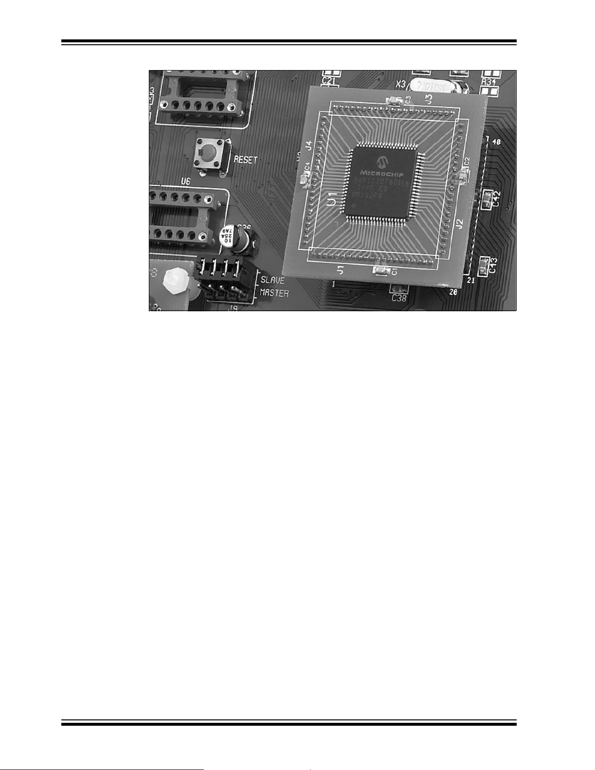
• Preprogrammed dsPIC30F6014A Plug-in Module (Figure 1-2)
• 9V DC Power Supply
• RS-232 Interface Cable
• dsPICDEM™ 1.1 Plus Development Board Kit CD containing demonstration
programs
FIGURE 1-1: dsPICDEM™ 1.1 PLUS DEVELOPMENT BOARD
5
2
7
10
26
9
8 7
8
6
27
25
13
4
3
3
11
10
5
14
1
12
4
18
1
16
© 2006 Microchip Technology Inc. DS70099D-page 9
Page 14
dsPICDEM™ 1.1 Plus Development Board User’s Guide
FIGURE 1-2: dsPIC30F6014A PLUG-IN MODULE
1.4 dsPICDEM™ 1.1 PLUS DEVEL OPMENT BOARD FEATURES
The dsPICDEM™ 1.1 Plus Development Board supports the following features:
Development Board Power
• Separate on-board +5V and +3.3V regulators for VDD and AVDD with direct input
from 9V, AC/DC wall adapter
• 9V DC power source input jack for development board
• LED power-on indicator
MPLAB ICD 2 and MPLAB ICE 4000 Connections
• MPLAB ICD 2 programming connector
• Jumper J8 for selection of processor interfaced to the MPLAB ICD 2
Debugger/Programmer
• Emulation header for connection to MPLAB ICE 4000 Emulator
• Pad location for 80-pin TQFP dsPIC DSC device
Serial Communication Channels
• Two RS-232 communication channels
• 6-pin terminal block and configuration jumper for RS-485 and RS-422
communication on UART1 from the dsPIC DSC device
• Single CAN communication channel
DS70099D-page 10 © 2006 Microchip Technology Inc.
Page 15

Introduction
Voice Band Codec
• Si3000 Voice band Codec chip (U7)
• Jumper J9 for selection of Si3000 Codec mode (Master/Slave)
• Socket U6, optional clock oscillator for Si3000 Voice band Codec
• 4-pin header for the Codec Line In and Line Out
• One 3.5 mm phono jack for the Codec left and right speaker outputs
• One 3.5 mm phono jack for the Codec MIC input
• Codec reset push button switch
Analog
• Three 5 kΩ Potentiometers (RP1-RP3)
• Microchip TC1047A Thermal Sensor (U9)
• MCP41010 Digital Potentiometer (U8)
• MCP602 Operational Amplifiers configured as low-pass filters for temperature
sensor and digital potentiometer (U10)
Device Clocking
• 7.3728 MHz crystal (X3) for dsPIC DSC device
• Socket U5, clock oscillator for dsPIC DSC device (alternate clock source, X3
removed)
• Pad for 32.768 kHz crystal (X2) and load caps
Miscellaneous
• Reset push button switch and jumper (J10) for resetting the PIC18F242 LCD
controller or the dsPIC DSC device
• Four red LEDs (LED1-LED4)
• Four push button switches (SW1-SW4) for external input stimulus
• 122 x 32 dot addressable LCD
• PIC18F242 LCD controller
• 2 x 50 prototyping header for user hardware expansion (header not installed)
• Prototype area for user hardware
1.5 SUPPORTED PLUG-IN MODULES
The dsPICDEM™ 1.1 Plus Development Board supports these Plug-In Modules:
• dsPIC30F6014A 80L Plug-In Module (MA300014)
• dsPIC33FJ256GP710 100-to-80L Plug-In Module (MA330012)
© 2006 Microchip Technology Inc. DS70099D-page 11
Page 16

dsPICDEM™ 1.1 Plus Development Board User’s Guide
1.6 RUNNING THE dsPICDEM™ 1.1 PLUS DEMONSTRATION PROGRAM
The dsPICDEM™ 1.1 Plus Development Board is supplied with a pre-loaded demonstration program that exercises principal CPU functions and peripheral options that
interact with typical user application programs.
When you apply power to the dsPICDEM™ 1.1 Plus Development Board, the LCD
menu displays these demonstration functions:
• Data Acquisition Display
• Digital Signal Processing (DSP) Operations
• Dual Tone Multi-Frequency (DTMF) Generation
Switches SW2-SW4 select one of these three choices. Each choice offers a submenu,
which provides for additional options using switches SW1-SW4.
Refer to Chapter 3. “dsPIC30F Demonstration Program Operation” for full details
on the demonstration code operation .
DS70099D-page 12 © 2006 Microchip Technology Inc.
Page 17

Chapter 2. Using dsPIC30F Devices
2.1 INTRODUCTION
This chapter is a self-paced tutorial to get you started using the dsPICDEM™ 1.1 Plus
Development Board with dsPIC30F devices. The tutorial demonstrates the main features of MPLAB IDE Integrated Development Environment and the MPLAB ICD 2
In-Circuit Debugger as they are used with the dsPICDEM™ 1.1 Plus Development
Board. Upon completing this tutorial, you should be able to:
• Create a project using the Project Wizard.
• Assemble and link the code and set the Configuration bits.
• Set up MPLAB IDE to use the MPLAB ICD 2 In-Circuit Debugger.
• Program the chip with the MPLAB ICD 2.
• View the code execution in program memory and source code.
• View registers in a Watch window.
• Set a breakpoint and make the code halt at a chosen location.
• Use the function keys to Reset, Run, Halt and Single Step the code.
dsPICDEM™ 1.1 PLUS
DEVELOPMENT BOARD
USER’S GUIDE
2.2 HIGHLIGHTS
Items discussed in this chapter include:
• Tutorial Overview
• Creating the Project
• Building the Code
• Programming the Chip
• Debugging the Code
2.3 TUTORIAL OVERVIEW
The tutorial program in Tut6014a.s (included with the CD-ROM) is written in
assembly code. This program displays text on the LCD and flashes an LED. The
source file is used with a linker script file (p30f6014a.gld) and an include file
(p30f6014a.inc) to form a comple te proje ct. The tutoria l is a si mple pr oject th at uses
a single source code file. More complex projects might use multiple assembler and
compiler source files as well as library files and precompiled object files. For simplicity ,
this tutorial uses only one source file.
There are four steps to this tutorial:
1. Create a project in MPLAB IDE.
2. Assemble and link the code.
3. Program the chip with the MPLAB ICD 2.
4. Debug the code with the MPLAB ICD 2.
© 2006 Microchip Technology Inc. DS70099D-page 13
Page 18
dsPICDEM™ 1.1 Plus Development Board User’s Guide
2.4 CREATING THE PROJECT
The first step is to create a project and a workspace in MPLAB IDE. Usually, you will
have one project in one workspace.
Note: These instructions presume the use of MPLAB 7.20 or newer.
A project contains the files needed to build an application (source code, linker script
files, etc.) along with their associations to various build tools and build options.
A workspace contains one or more projects and information on the selected device,
debug tool and/or programmer, open windows and their location and other IDE
configuration settings.
MPLAB IDE contains a Project Wizard to help create new projects. Before starting,
create a folder for the project files for this tutorial (C:\Tutorial is assumed in the
instructions that follow). From the dsPICDEM 1_1 Plus Development Board
code\Tutorial Code folder on the dsPICDEM™ 1.1 Plus Development Kit CD,
copy the Tut6014a.s file into the C:\Tutorial fold er.
Note: All files copied from the CD are read only. If the file needs to be edited, the
attributes will need to be changed.
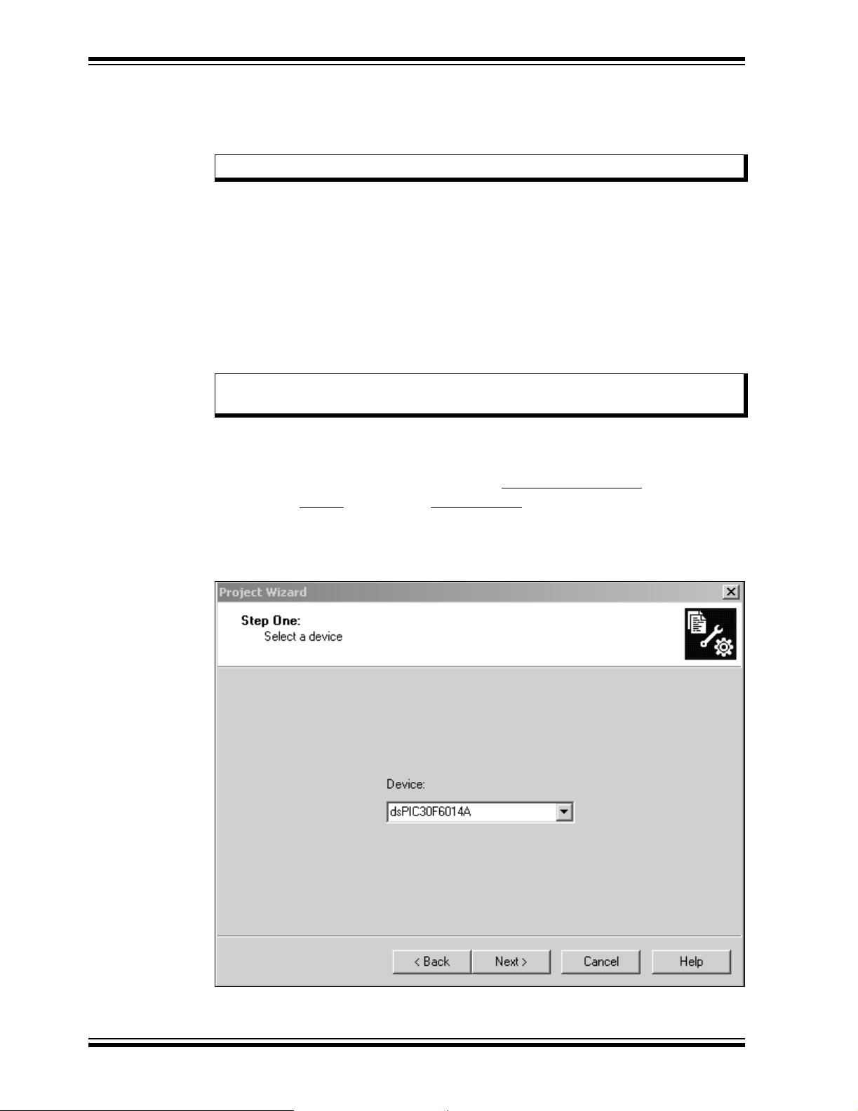
2.4.1 Select a Device
1. Start MPLAB IDE.
2. Close any workspace that might be open (File>Close Workspace
3. From the Project
4. From the Welcome screen, click Next> to display the Project Wizard Step One
dialog (see Figure 2-1).
FIGURE 2-1: PROJECT WIZARD, STEP 1, SELECT A DEVICE
menu, select Project Wizard.
).
DS70099D-page 14 © 2006 Microchip Technology Inc.
Page 19
Using dsPIC30F Devices
5. From the Device: pull-down list, select dsPIC30F6014A and click Next>. The
Project Wizard Step Two dialog displays (see Figure 2-2).
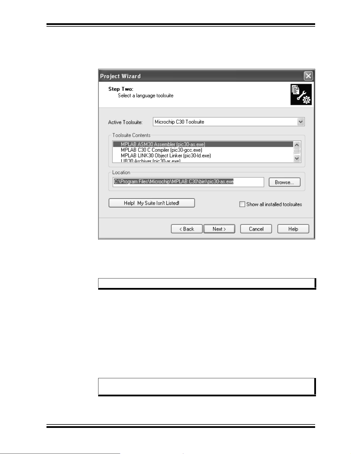
FIGURE 2-2: PROJECT WIZARD, STEP 2, SELECT LANGUAGE
TOOLSUITE
2.4.2 Select Language Toolsuite
1. From the Active Toolsuite: pull-down menu, select Microchip C30 Toolsuite.
This toolsuite includes the assembler and linker that will be used (the C Compiler
is not used).
Note: Steps 2-4 are optional.
2. In the Toolsuite Contents block, select MPLAB ASM30 Assembler
(pic30-as.exe).
3. In the Location block, click Browse... and navigate to:
C:\Program Files\Microchip\MPLAB ASM30 Suite
\bin\pic30-as.exe
4. With MPLAB LINK 30 Object Linker (pic30-Id.exe) selected in Toolsuite
Contents, click Browse... and navigate to:
C:\Program Files\Microchip\MPLAB ASM30 Suite
\bin\pic30-id.exe
5. Click Next> to continue. The Project Wizard Step Three dialog displays
(see Figure 2-3).
Note: The tool locations for your environment may be different from those shown
in this tutorial.
© 2006 Microchip Technology Inc. DS70099D-page 15
Page 20
dsPICDEM™ 1.1 Plus Development Board User’s Guide
FIGURE 2-3: PROJECT WIZARD, STEP 3, NAME YOUR PROJECT
2.4.3 Name Your Project
1. In the Project Name text box, type MyProject.
2. Click Browse... and navigate to C:\Tutorial to place your project in the
Tutorial folder.
3. Click Next> to continue. The Project Wizard Step Four dialog displays
(see Figure 2-4).
DS70099D-page 16 © 2006 Microchip Technology Inc.
Page 21
Using dsPIC30F Devices
FIGURE 2-4: PROJECT WIZARD, STEP 4, ADD FILES TO PROJECT
2.4.4 Add Files to Project
1. Locate the C:\Tutorial folder and select the Tut6014A.s file.
2. Click Add>> to include the file in the project.
3. Expand the C:\Program Files\Microchip\MPLAB ASM30 Suite\Sup-
port\gld folder and select the p30f6014A.gld file.
4. Click Add>> to include the file in the project. The project now has two files.
5. Click Next> to continue.
6. When the summary screen displays, click Finish.
After the project wizard completes, the MPLAB IDE project window shows the
Tut6014A.s file in the Source Files folder and the p30f6014A.gld file in the Linker
Scripts folder (see Figure 2-5).
FIGURE 2-5: MPLAB
®
IDE PROJECT WINDOW
© 2006 Microchip Technology Inc. DS70099D-page 17
Page 22
dsPICDEM™ 1.1 Plus Development Board User’s Guide
A project and workspace has now been created in MPLAB IDE. MyProject.mcw is
the workspace file and MyProject.mcp is the project file. Double click the
Tut6014A.s file in the project window to open the file. MPLAB IDE should now look
similar to Fi gu r e 2-6.
FIGURE 2-6: MPLAB
®
IDE WORKSPACE WINDOWS
DS70099D-page 18 © 2006 Microchip Technology Inc.
Page 23

2.5 BUILDING THE CODE
In this project, building the code consists of assembling the Tut6014A.s file to create
an object file, Tut6014A.o, and then linking the object file to create the
Tut6014A.hex and Tut6014A.cof output files. The .hex file contains the data necessary to program the device and the .cof file contains additional information that lets
you debug at the source code level.
Before building, there are settings required to tell MPLAB IDE where to find the include
files and to reserve space for the extra debug code when the MPLAB ICD 2 is used.
The following line is near the top of the Tut6014A.s file:
.include "p30f6014A.inc"
This line causes a standard include file to be used. Microchip provides these files with
all the Special Function Register (SFR) labels already defined for convenience.
To build the code, select Build Option s>Project
Options dialog displays, as shown in Figure 2-7.
FIGURE 2-7: BUILD OPTIONS
Using dsPIC30F Devices
from the Project> menu. The Build
Browse to the location of the
assembler Include folder.
© 2006 Microchip Technology Inc. DS70099D-page 19
Page 24
dsPICDEM™ 1.1 Plus Development Board User’s Guide
2.5.1 Identify Assembler Include Path
1. Select the General tab.
2. At the Assembler Include Path, $(AINDIR) box, click Browse... and navigate
to:
C:\Program Files\Microchip\MPLAB ASM30 Suite\Support\Inc
This path tells MPLAB IDE where to find the Include files.
2.5.2 Link for ICD 2
1. Select the MPLAB LINK30 tab to view the linker settings (see Figure 2-8).
2. Check Link for ICD 2.
3. Click Apply, then click OK. The text box closes while the linker reserves space
for the debug code used by the MPLAB ICD 2.
4. Click OK again to save these changes. The project is now ready to build.
FIGURE 2-8: MPLAB
®
LINK30 BUILD OPTIONS
Check Link for ICD2
DS70099D-page 20 © 2006 Microchip Technology Inc.
Page 25
Using dsPIC30F Devices
2.5.3 Build the Project
1. Select P r oj ect >B ui ld All.
2. Observe the progress of the build in the Output window (Figure 2-9).
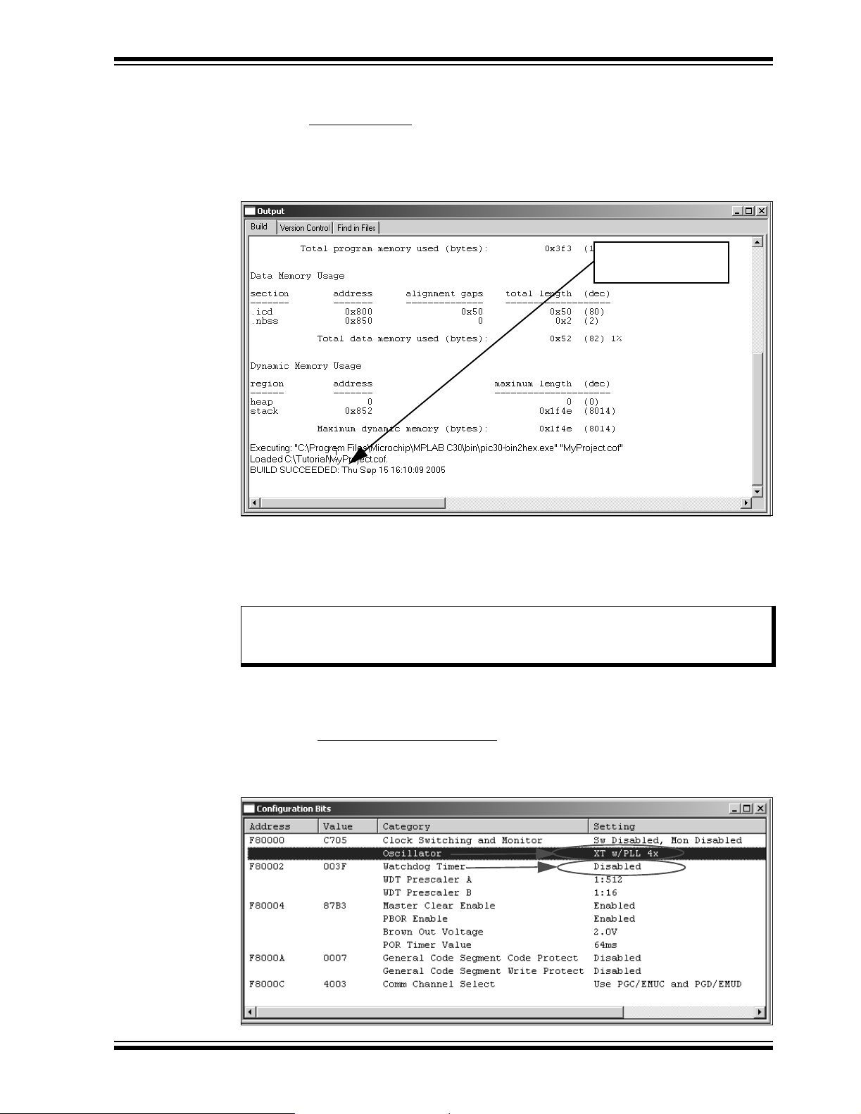
3. When BUILD SUCCEEDED displays you are ready to program the device.
FIGURE 2-9: BUILD OUTPUT WINDOW
2.6 PROGRAMMING THE CHIP
The MPLAB ICD 2 In-Circuit Debugger can be used to program and debug the
dsPIC30F6014A device in-circuit on the dsPICDEM™ 1.1 Plus Development Board.
Note: Before proceeding, make sure that the USB driver for the MPLAB ICD 2 has
been installed on your PC (see the “MPLAB
DS51331) for more details regarding the installation of MPLAB ICD 2.
Status shows
BUILD SUCCEEDED
®
ICD 2 User’s Guide”,
Use the following procedures to program the dsPIC30F6014A device.
2.6.1 Set Up the Device Configuration
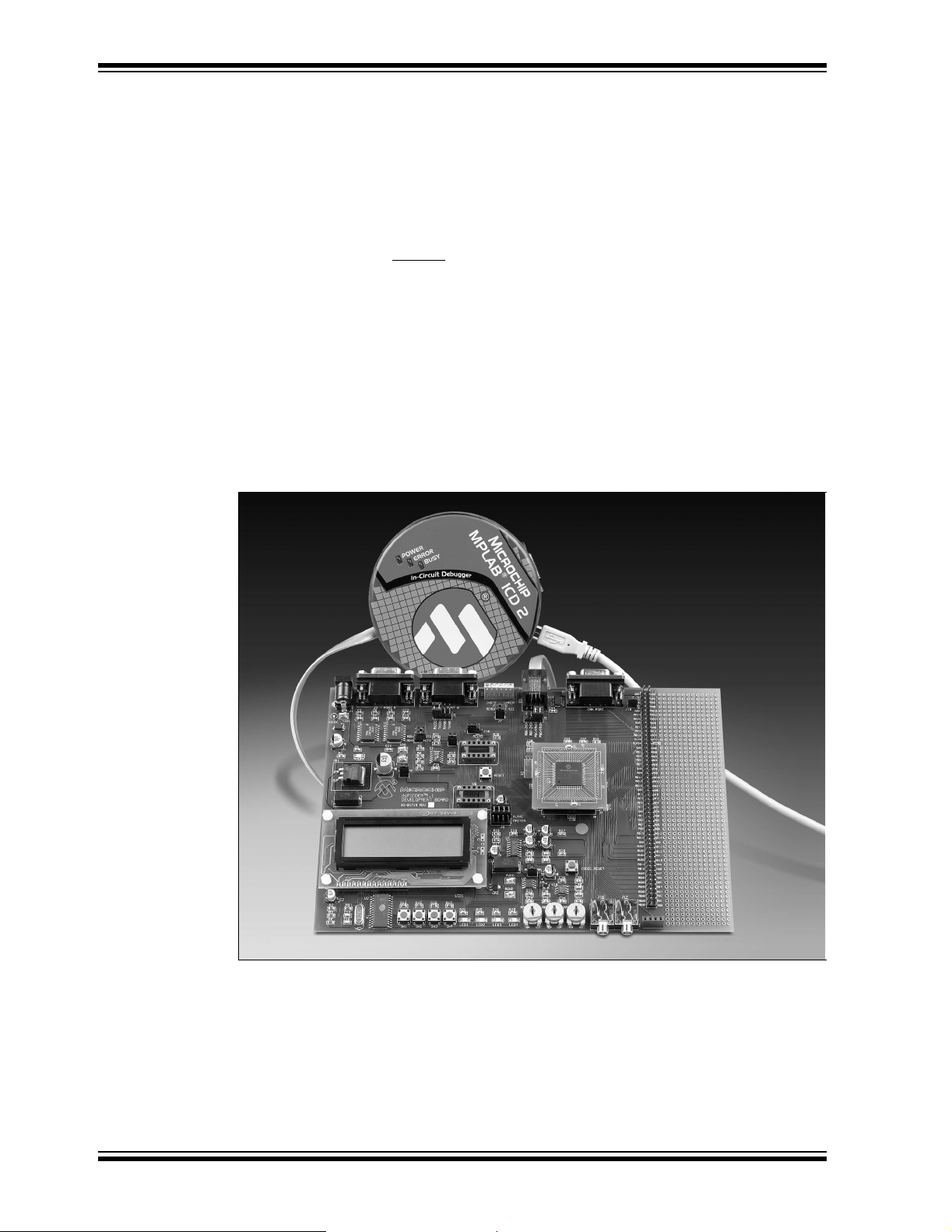
1. Use the Configure>Configuration Bits menu to display the configuration settings.
2. Set up the Configuration bits as shown in Figure 2-10.
FIGURE 2-10: CONFIGURATION SETTINGS
© 2006 Microchip Technology Inc. DS70099D-page 21
Page 26
dsPICDEM™ 1.1 Plus Development Board User’s Guide
The highlighted configuration settings may need to change to the these values:
Primary Oscillator Mode: XT w/PLL 4x
Watchdog Timer: Disabled
2.6.2 Connect the MPLAB ICD 2 In-Circuit Debugger
1. Before set ting up the hardware, check that the following jumpers are in place:
AVDD_JMP: On
J8: 33F PGD3/30F, 33F PGD3/30F
J10: MCLR1
VDD_JMP: On
J21 On (5V)
J22 On (5V)
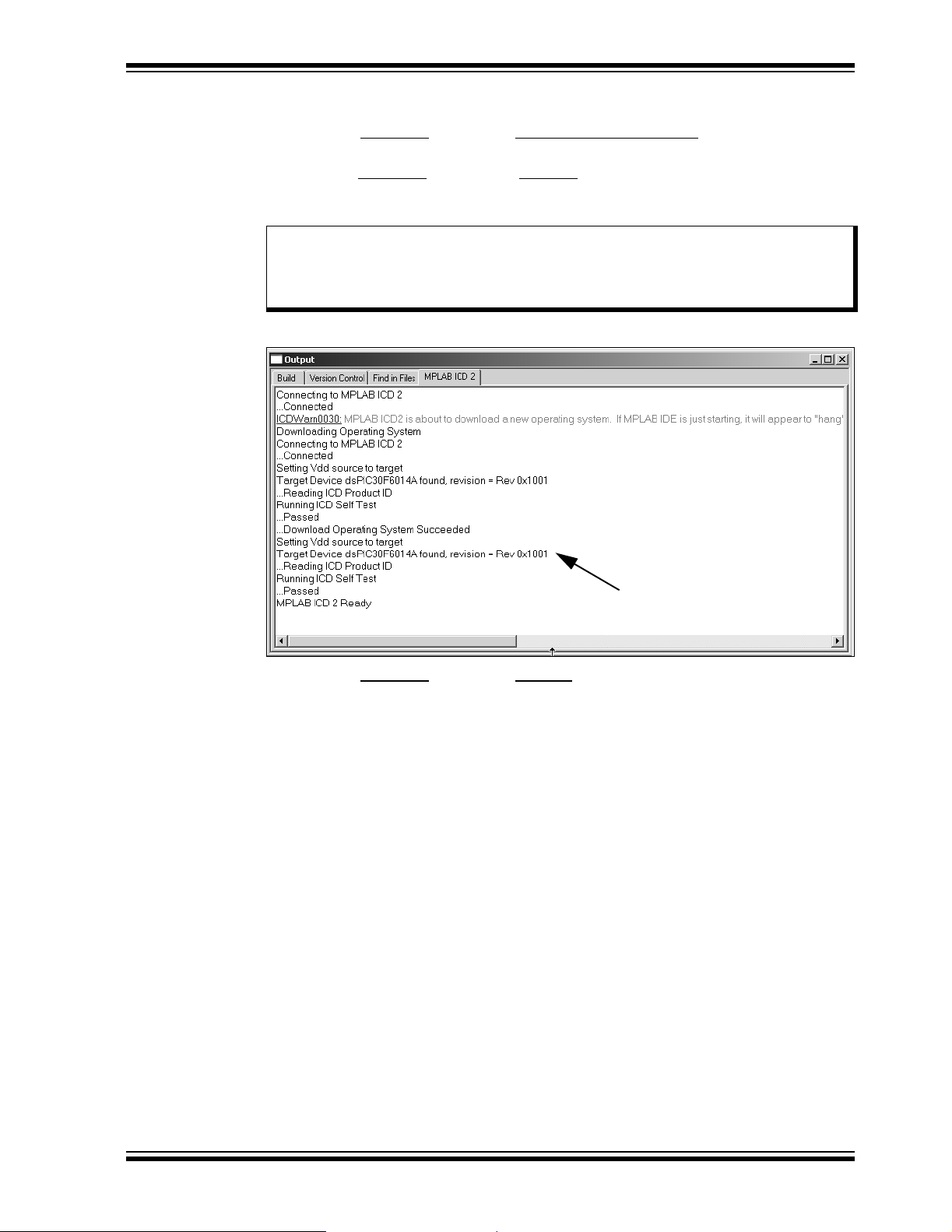
2. Connect the MPLAB ICD 2 to the PC with the USB cable (see Figure 2-11).
3. Connect the MPLAB ICD 2 to the dsPICDEM™ 1.1 Plus Development Board
with the short RJ-11 (telephone) cable.
4. Apply power to the board.
FIGURE 2-11: dsPICDEM™ 1.1 PLUS DEVELOPMENT BOARD
CONNECTED TO MPLAB
®
ICD 2 IN-CIRCUIT DEBUGGER
DS70099D-page 22 © 2006 Microchip Technology Inc.
Page 27
Using dsPIC30F Devices
2.6.3 Enable MPLAB ICD 2 Connection
1. From the Debugger menu, click Select Tool>MPLAB ICD 2 to designate the
MPLAB ICD 2 as the debug tool in MPLAB IDE.
2. From the Debugger
The MPLAB ICD 2 should report that it found the dsPIC30F6014A device, as
shown in Figure 2-12.
Note: MPLAB IDE may need to download new firmware if this is the first time the
MPLAB ICD 2 is being used with a dsPIC30F device. Allow it to do so. If
any errors are shown, double click the error message to get more
information.
menu, select Connect to connect the debugger to the device.
FIGURE 2-12: ENABLING MPLAB
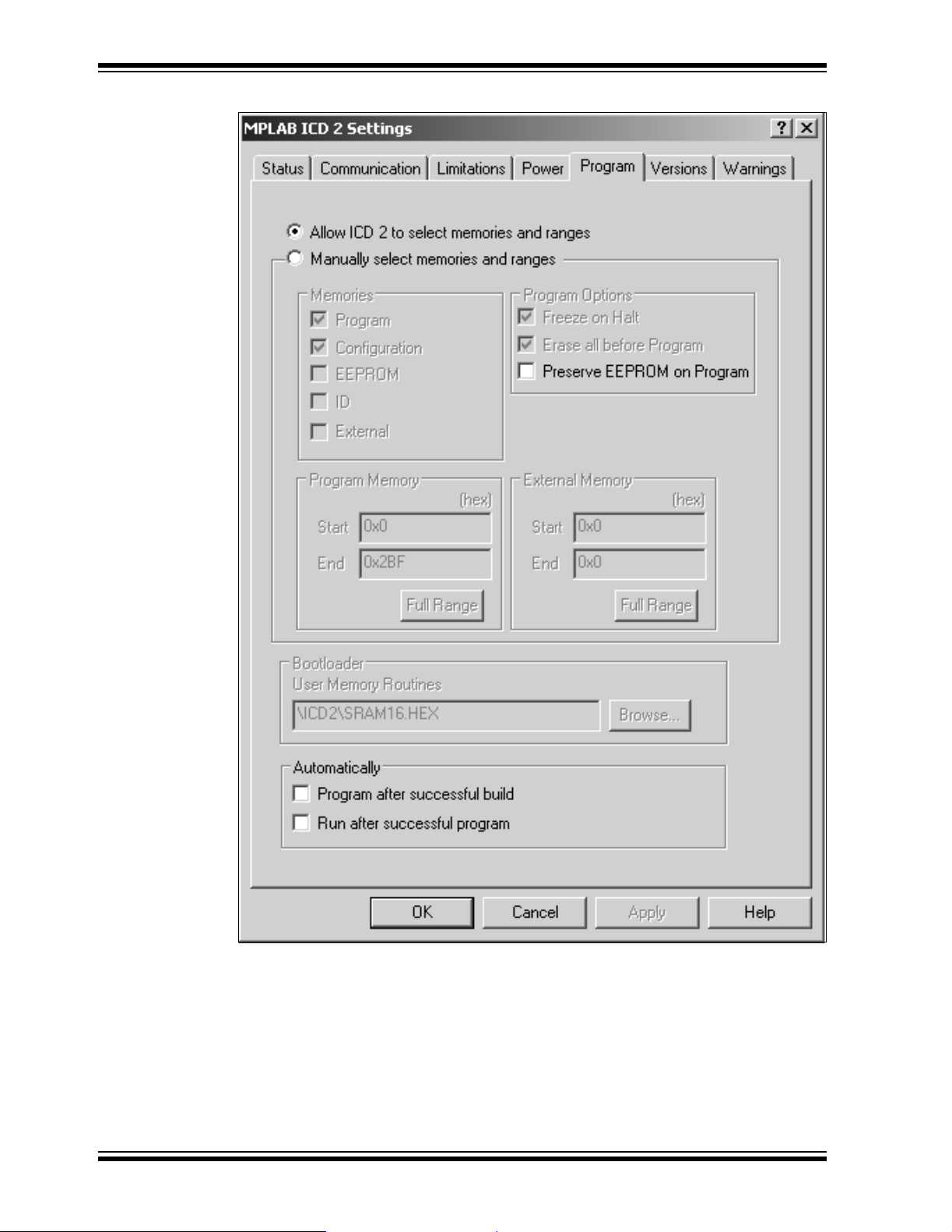
3. From the Debugger
menu, click Settings to display the MPLAB ICD Debugger
®
ICD 2
Status shows that target
device has been found
.
settings.
4. Select the Program tab.
5. Check Allow ICD 2 to select memories and ranges, as shown in Figure 2-13.
This setting will speed up operations by programming only a small part of the
total program memory.
© 2006 Microchip Technology Inc. DS70099D-page 23
Page 28
dsPICDEM™ 1.1 Plus Development Board User’s Guide
FIGURE 2-13: SETTING PROGRAM MEMORY SIZE
DS70099D-page 24 © 2006 Microchip Technology Inc.
Page 29

Using dsPIC30F Devices
2.6.4 Program the dsPIC30F6014A Device
1. From the Debugger menu, select Program. The Output window (Figure 2-14)
displays the program steps as they occur.
2. Observe the process in the Output window. When “MPLAB ICD 2 Ready”
displays, the device is programmed and ready to run.
FIGURE 2-14: PROGRAMMING THE dsPIC30F6014A DEVICE
3. Use the Debugger>Reset
code. LED1 should start blinking and the LCD display should show the text in
Figure 2-15.
FIGURE 2-15: TUTORIAL LCD DISPLAY
2.7 DEBUGGING THE CODE
The MPLAB ICD 2 In-Circuit Debugger can be used to run, halt and step the code. A
breakpoint can be set to halt the program after the code has executed the instruction
at the breakpoint. The contents of the RAM and registers can be viewed whenever the
processor has been halted.
The MPLAB ICD 2 In-Circuit Debugger uses the following function keys to access the
main debugging functions:
<F5> Halt
<F6> Reset
<F7> Single Step
<F9> Run
In addition, there are more functions available by right clicking on a line of source code.
The most important of these are “Set Breakpoint” and “Run to Cursor”.
menu to reset the code, then Debugger>Run to run the
DSPIC30F 16-BIT
DIGITAL SiGNAL
CONTROLLER
© 2006 Microchip Technology Inc. DS70099D-page 25
Page 30

dsPICDEM™ 1.1 Plus Development Board User’s Guide
2.7.1 Display the Code
1. From the View menu, select Program Memory.
2. On the Program Memory window, select the Symbolic tab, as shown in
Figure 2-16.
FIGURE 2-16: PROGRAM MEMORY WINDOW
3. Press <F5> to halt the processor and press <F6> to reset. The program memory
now shows a green arrow pointing to the line of code at address 0, the reset
location.
The instruction at this location is goto __reset. This code is added by the
linker to make the program branch to the start of the code in the Tut6014A.s
file. The code uses the __reset label at the start of the executable code and
declares the label as global to have visibility outside the source file
(see Example 2-1).
EXAMPLE 2-1: CODE START-UP
.global __reset
.text
__reset: mov #__SP_init, W15
mov #__SPLIM_init, W0
mov W0, SPLIM
The linker also provides values for the __SP_init and __SPLIM_init
constants to initialize the stack pointer (W15), since the linker determines what
RAM is available for the stack.
DS70099D-page 26 © 2006 Microchip Technology Inc.
Page 31

Using dsPIC30F Devices
2.7.2 Step the Program
1. Press <F7> to single step the code. The green arrow now points to the code at
__reset in the Tut6014A.s source code as shown in Figure 2-17.
2. Right click the line of code mov w0,LATD and choose Run to Cursor
arrow then points to the line mov w0,TRISD, because it has executed the prior
lines of code up to and including mov #0xFFF0,w0.
FIGURE 2-17: SOURCE CODE WINDOW
. The green
3. From the View
4. From the Add SFR pull-down list, display TRISD.
5. Click Add SFR to add the TRISD register to the Watch window.
6. Next, select PORTD from the pull-down list and click Add SFR.
7. Press <F7> a few times and watch the values of TRISD and PORTD SFRs
change.
FIGURE 2-18: WATCH WINDOW DISPLAY
Note: The value displayed for PORTD may be different on your system
depending on what load is on PORTD.
menu, select Watch to open a Watch window (Figure 2-18).
© 2006 Microchip Technology Inc. DS70099D-page 27
Page 32

dsPICDEM™ 1.1 Plus Development Board User’s Guide
2.7.3 Set Breakpoint
1. To set a breakpoint, right click a code line and select Set Breakpoint from the
pop-up menu.
Note: An alternate method is to simply double click the line. This feature may
need to be enabled using the Edit>Properties
As an example, find the following line of code and set a breakpoint on this line.
WrtNextChr: btss flags, #0
A red stop sign should appear in the gutter (gray bar on the left) of the source
code window.
2. Press <F9> to run the code. The program halts on the instruction following the
breakpoint as shown in Figure 2-19.
Note: The instruction on which the code halts could be elsewhere in the code if
the breakpoint was set on or immediately after a branch instruction. Refer
to Section 12, “Important Notes”, in the Readme file for the MPLAB
ICD 2.txt file located in the E:\MPLAB IDE\READMES directory for
additional operational information.
FIGURE 2-19: SETTING BREAKPOINT
menu.
In this example, every time <F9> is pressed to run the code it sends one character to
the display and stops at the breakpoint. After the first four spaces, the characters will
start to appear on the LCD display.
DS70099D-page 28 © 2006 Microchip Technology Inc.
Page 33

dsPICDEM™ 1.1 PLUS
DEVELOPMENT BOARD
USER’S GUIDE
Chapter 3. dsPIC30F Demonstration Program Operation
3.1 INTRODUCTION
A dsPIC30F DSC device shipped with the dsPICDEM™ 1.1 Plus Development Board
includes a pre-programmed demonstration program. This demonstration program
exercises several of the dsPIC30F peripherals, such as the 12-bit Analog-to-Digital
Converter (ADC) and Codec interface and several of the unique CPU features. This
chapter discusses these examples and explains the functionality they demonstrate. For
detailed information on the dsPICDEM™ 1.1 Plus Development Board hardware, refer
to Chapter 5. “dsPICDEM™ 1.1 Development Hardware”.
3.2 HIGHLIGHTS
Items discussed in this chapter are:
• Demonstration Program Operat ion
• Data and Control Flow
• dsPIC30F Demonstration Performance Metrics
• Board Self-Test Code Module Summary
3.3 DEMONSTRATION PROGRAM OPERATION
The dsPIC30F device included with your dsPICDEM™ 1.1 Plus Development Board is
programmed to automatically initiate the demonstration code when power is applied to
the board. This code is divided into two separate modules:
• Demonstration code module
• Board self-test code module
This chapter is mostly devoted to describing the demonstration program. The end of
the chapter includes a brief summary of the board self-test code module, which has
been included on the CD as a library archive only. See 3.6 “Board Self-Test Code
Module Summary”.
3.3.1 Demonstration Code Module Summary
When power is applied to the dsPICDEM™ 1.1 Plus Development Board, the LCD
displays the Demo Main Menu, as shown in Figure 3-1.
FIGURE 3-1: POWER-UP DISPLAY
dsPIC30F 16-BIT
DIGITAL SIGNAL
CONTROLLER
DEMO MAIN MENU – S1
From this menu, pressing switch SW1 displays the menu options for the demonstration
program, as shown in Figure 3-2.
© 2006 Microchip Technology Inc. DS70099D-page 29
Page 34

dsPICDEM™ 1.1 Plus Development Board User’s Guide
FIGURE 3-2: DEMO MENU OPTIONS
MENU OPTIONS
DATA ACQ DISPLAY –S2
DSP OPERATIONS –S3
DTMF GENERATION –S4
From this menu you can choose one of three demonstration modes:
• Data Acquisition Display mode
• Digital Signal Processing (DSP) Operations mode
• Dual Tone Multi-Frequency (DTMF) Generation mode
3.3.1.1 DATA ACQUISITION DISPLAY MODE The Data Acquisition Display mode demonstrates the capability of the dsPIC30F
device to convert inputs from five different analog signal sources at varying sampling
rates.
Data Acquisition mode is initiated by pressing switch SW2. Figure 3-3 shows the
resulting display on the LCD.
FIGURE 3-3: DATA ACQUISITION DISPLAY
F = 1000HZ TEMP = +23DGC
RP1 = 1.67V RP2 = 2.95V
RP3 = 2.62V
MAIN – s1
This display shows the values of the following analog signal sources:
• Potentiometers RP1-RP3
The three potentiometers available on the dsPICDEM™ 1.1 Plus Development
Board, RP1, RP2 and RP3, are connected to analog input pins AN6, AN4 and
AN5, respectively, on the dsPIC30F device.
• Temperature Sensor U9:
T emperature sensor, TC1047A, is connected to the analog input pin, AN8, on the
dsPIC30F device.
• Frequency:
A fundamental sine-wave signal is generated by stepping the MCP41010 digital
potentiometer (U8) output at an 8 kHz rate. The analyzed frequency is displayed
on the LCD.
The 12-bit ADC on the dsPIC30F device is used to convert these analog input sources.
T o estimate the frequency of the generated sine-wave signal, the program converts and
buffers 256 samples of the signal on pin AN3 and then performs a Fast-Fourier
Transform (FFT) on the buffer. The ADC is interrupt driven to sample and convert at a
16 kHz rate for this operation. AN3 is converted on every alternate conversion, thus
delivering an effective sampling rate of 8 kHz for the signal presented at AN3.
The program scans input pins AN4, AN5, AN6 and AN8 to sample and convert the
values of the temperature sensor and potentiometer signals and delivers one sample
of each of these signals to the LCD display.
DS70099D-page 30 © 2006 Microchip Technology Inc.
Page 35

dsPIC30F Demonstration Program Operation
Y ou can also display the data acquisition values on the communications HyperT erminal
on your PC. Use a DB-9 cable to connect “J2 – PORT A” on the development board to
the RS-232 serial port on the PC, as shown in Figure 3-4.
FIGURE 3-4: dsPICDEM™ 1.1 PLUS DEVELOPMENT BOARD TO PC
CONNECTION
Development Board
J2
DB-9 Cable
After connecting the table, configure HyperTerminal for the port settings shown in
Figure 3-5. HyperTerminal will show a composite display of the data acquisition values
at an update rate of 1.14 seconds.
FIGURE 3-5: HYPERTERMINAL CONFIGURATION SETTINGS
PC
RS-232
Port
To return to the Menu Options display after running the Data Acquisition demo, press
switch SW1.
© 2006 Microchip Technology Inc. DS70099D-page 31
Page 36

dsPICDEM™ 1.1 Plus Development Board User’s Guide
3.3.1.2 DSP OPERATIONS MODE
From the Menu Options display, pressing switch SW3 launches the DSP Operations
demo, which displays the digital signal values shown in Figure 3-6. This display
provides information on the various signal processing operations that are performed on
the signal at analog input pin, AN3.
FIGURE 3-6: DSP OPERATIONS DISPLAY
F = 1000 BIN = 032
256 PT TFFT =018175CY
I I R TFILT =028649CY
MAIN – s1 CHNGFILT – S2
The DSP operations display shows several parameters for a sampled sine-wave
signal. A fundamental sine-wave signal is generated by stepping the MCP41010 digital
potentiometer (U8) output at an 8 kHz rate. The output of the digital potentiometer is
applied to a Low-Pass (LP) filter with a cutoff frequency of approximately 4 kHz. This
LP filter removes the high-frequency components and yields a sine wave adequate for
this demonstration. Five frequencies are developed and selected by varying
potentiometer RP1, as shown in Table 3-1.
TABLE 3-1: FREQUENCIES VS. POTENTIOMETER SETTING
Potentiometer Setting Resulting Frequency
0 ≤ RP1 ≤ 1V 100 Hz
1 ≤ RP1 ≤ 2V 500 Hz
2 ≤ RP1 ≤ 3V 1000 Hz
3 ≤ RP1 ≤ 4V 1500 Hz
4 ≤ RP1 ≤ 5V 2000 Hz
The filtered output of the MCP41010 is routed to pin AN3/RB3, which is an input to the
12-bit ADC. The ADC collects 256 samples from the MCP41010 at an 8 kHz sample
rate. These samples are optionally subjected to a digital filtering algorithm. The
following three digital filtering options are provided and selected by switch SW2:
•None
• Infinite Impulse Response (IIR)
• Finite Impulse Response (FIR)
Subsequently, their spectral components are estimated. The frequency estimate of the
signal on pin AN3/RB3 is displayed on the first row of the DSP Operations display.
DS70099D-page 32 © 2006 Microchip Technology Inc.
Page 37

dsPIC30F Demonstration Program Operation
Figure 3-7 depicts the flow of data from the time the analog input is converted by the
dsPIC30F device to the time the frequency is estimated.
FIGURE 3-7: DSP OPERATIONS FLOW DIAGRAM
T
FILT
Generated
Sine Wave
Low-Pass
Filter
x1(t) x2(t) x[n]
To display
on LCD
ADC
12-bit,
8 kHz sampling
Magnitude
computation and
peak-frequency
detection
Bandpass
IIR/FIR filter
y[n]
256-point FFT
X
2
FFT
T
FFT
Figure 3-8 shows the frequency response of the IIR filter implementation. The IIR filter
is only employed for demonstrating filter operation.
FIGURE 3-8: FREQUENCY RESPONSE: IIR FILTER
© 2006 Microchip Technology Inc. DS70099D-page 33
Page 38

dsPICDEM™ 1.1 Plus Development Board User’s Guide
Figure 3-9 shows the frequency response of the FIR filter implemented on the
dsPIC30F. The FIR filter is only employed for demonstrating filter operation.
FIGURE 3-9: FREQUENCY RESPONSE: FIR FILTER
The signal frequency determined by analyzing the 256-point FFT and associated bin is
displayed on the LCD. Cycle counts for the digital filters and FFT are displayed on the
LCD.
To quit this demonstration and return to the main menu, press switch SW1.
3.3.1.3 DTMF GENERATION MODE
From the Me nu O pti ons disp lay, pressing sw it ch SW4 lau nche s th e DT MF Ge nera tio n
demo and takes you to the DTMF operation menu (Figure 3-10).
FIGURE 3-10: DTMF TONE GENERATION MENU
DTMF TONE 0123456789
NEXT –s2
SELECT –s3
PLAY SEQ –s4 MAIN –s1
When this display is active, switches SW2-SW4 control tone generation, as shown in
Table 3-2.
TABLE 3-2: DTMF TONE GENERATION CONTROLS
Switch Function
SW2 Moves blinking cursor to the next DTMF Tone digit
SW3 Plays the DTMF tone associated with the digit selected by s2
SW4 Plays a predetermined sequence of ten DTMF tones
DS70099D-page 34 © 2006 Microchip Technology Inc.
Page 39

dsPIC30F Demonstration Program Operation
Each DTMF tone consists of two sinusoids: a high-frequency component and a lowfrequency component. In the DTMF tones implemented for this demonstration, the
high-frequency component is at a level 8 dB lower than the low-frequency component.
You can listen to the generated tones by using either a headset or a passive speaker
connected to the “SPKR OUT” jack (J17).
Note: For a passive speaker, use a Radio Shack Model # 40-1434 Fold-up Stereo
Speaker System or an equivalent device.
If you connected your PC for the Data Acquisition Display demo (see Section 3.3.1.1),
you can use the <0>-<9> keys on the PC keyboard to select a DTMF tone.
To quit this demonstration and return to Menu Options, press switch SW1.
3.3.2 Demonstrated Features and Peripherals
The following two sections summarize the key dsPIC30F MCU, DSP and peripheral
features implemented in this general purpose demonstration program.
3.3.2.1 dsPIC30F MCU/DSP FEATURES The demonstration program uses several unique dsPIC30F MCU/DSP features for
various processing functions, including:
• DSP Engine for FFT, FIR and IIR computations
- 40-bit accumulators with Saturation, Overflow and Rounding modes
- Multiply-and-Accumulate (MAC) class of DSP instructions
• Bit-Reversed Addressing for 256-point FFT input data in preparation for the FFT
“butterfly” computations
• Modulo Addressing for accessing arrays in a circular fashion for FIR filtering
- Two modulo buffers have been implemented, one each in X and Y data
spaces.
• Hardware Loop instructions
- DO and REPEAT instructions provide minimal overhead when executing a
block of instructions repetitively.
• Program Space Visibility (PSV)
- Large tables for FIR filter coefficients, sine tables etc., are stored in and
accessed from program memory.
3.3.2.2 dsPIC30F DEMO PERIPHERALS The demonstration program also implements several dsPIC30F peripherals for various
tasks. These peripherals include:
• Timer1 – Configured as a 16-bit timer
• Timer2 – Configured as 16-bit timer with a 256:1 prescaler
• Timer3 – Configured as 16-bit timer with a 256:1 prescaler
• Timer4 and Timer5 – Configured as a 32-bit timer
• UART2 TX/RX – Used to transmit demo data to the PC and receive commands
from the PC keyboard
• SPI 2 – Used to communicate to the 122 x 32 Addressable-Pixel LCD via the
PIC18F242 LCD controller and MCP41010 digital potentiometer
• 12-bit ADC – Used to convert multiple analog signals, including temperature and
sine-wave signals generated by the MCP41010 digital potentiometer through a
low-pass filter
© 2006 Microchip Technology Inc. DS70099D-page 35
Page 40

dsPICDEM™ 1.1 Plus Development Board User’s Guide
• Data Converter Interface – Interfaced to an external Si3000 voice band Codec for
transmission of DTMF PCM signals
• INTx pins – Used for detecting switch SW1-SW4 inputs
• Hierarchical/Prioritized Interrupt Control with nesting enabled
3.4 DATA AND CONTROL FLOW
3.4.1 Power-up Sequence
The power-up peripheral initialization sequence is shown in Table 3-3.
TABLE 3-3: POWER-UP PERIPHERAL INITIALIZATION SEQUENCE
Seq Module or Function Initialization Process
1 Timer1 Configured to count to 125 µS, but not enabled.
2 Timer2 Configured to count to 1 second using a 256:1 prescaler
setting.
3 Timer3 Configured to count up to 1.14 seconds using the 256:1
prescaler setting.
4 Timer4 and Timer5 Configured to operate in the 32-bit Timer mode, but not
enabled until needed.
5 Interrupt Service
Routine (ISR)
6 UART2 Both the transmitter and receiver are configured for
7 SPI 2 Initially configured to operate in an interrupt-driven mode at
8 Data Converter
Interface (DCI)
9 Si3000 Configured for Slave mode. The Si3000 line and speaker
10 DCI Re-initialized to o per ate w ith all fou r bu f fe r s in inte rrup t-dri ven
1 1 External interrupt
pins INT1-INT4
12 12-bit ADC Configured to operate at 16000 Hz sampling rate and gener-
13 Interrupts Peripheral interrupts are configured. Nested interrupts are
Processing is enabled for Timer2 and Timer3.
interrupt-driven operation at 57600 baud.
F
CY/8 Hz (where FCY = 7.3728 MHz). The module communi-
cates at F
LCD controller. When it is used to step the MCP41010, it
operates in the 16-bit mode at FCY/32 Hz.
Configured for Master mode. Initially configured to use two of
four buffers. T ransm its/rec eives in time slot 1 at the frame rate
of 7200 Hz for configuring the Si3000 external voice band
Codec.
ports are enabled. Signal attenuation is set to 0 dB. The ADC
input from the Si3000 is atten uated by 34.5 dB and is not used
in this demo.
mode for transmitting D TMF PCM wo rds to the Si3000 Codec.
Configured to interrupt on the falling edge and used for
switches SW1-SW4, respectively.
ate an interrupt every 16 sample-convert sequences. The
ADC samples channel AN3 (sine wave), AN4 (RP2), AN5
(RP3), AN6 (RP1) and AN8 (temperature sensor U9).
enabled.
CY/8 Hz in 8-bit mo de while displ aying resul ts on the
DS70099D-page 36 © 2006 Microchip Technology Inc.
Page 41

dsPIC30F Demonstration Program Operation
3.4.2 Main Loop Code Execution
The step-by-step Main Loop execution sequence is shown in Table 3-4.
TABLE 3-4: MAIN LOOP CODE EXECUTION SEQUENCE
Seq Program Task
1 12-bit ADC collects 256 samples from the digit al potentiomete r output on AN3 into
a RAM buffer. It also collects one sam ple ea ch f r om AN 4 (RP2), AN5 (RP3), AN6
(RP1) and AN8 (Temperature Sensor U9). All A/D conversions are performed in
an interrupt-driven configuration.
2 Buffered data set is filtered using an IIR filter to remove line noise. The filter can
be changed to an FIR filter or no filter from the DSP menu options. The filtering
operation is benchmarked using the Timer4/5 pair.
3 A complex in-place 256-point FFT is performed on the filtered data set, resulting
in complex frequency data (x + jy). This operation is benchmarked using the
Timer4/5 pair.
4 Squared magnitude is computed for each frequency bin in an in-place fashion
5 The magnitude data is run through a routine that returns the frequency bin and
6 The magnitude of the largest element is compared against a threshold and
7 If a Timer3 count has expired, a software flag is set to inform the CPU that the
8 Any user choices entered via the switches SW1-SW4 are checked and the new
9 The changes are communicated to the PIC18F242 LCD controller via the SPI 2
10 In the special case of the DTMF menu, the main routi ne may al so kick off the DCI
2
+ y2).
(x
magnitude of the largest element.
captured if it is greater than the threshold so that low-level noise does not show
up as a frequency estimate. (Provides a simplified peak-detection algorithm.)
results recorded ma y no w be dis played. This ensures that the CPU refreshes the
display buffers.
user selections are applied. May involve a change of display screen or some
parameter displayed on the LCD.
module.
module operation when the user requests DTMF tone generation.
© 2006 Microchip Technology Inc. DS70099D-page 37
Page 42

dsPICDEM™ 1.1 Plus Development Board User’s Guide
3.4.3 Interrupts Used in the Demo
3.4.3.1 EXTERNAL INTERRUPTS TO MAIN ROUTINE
External interrupts INT1-INT4 are controlled by switches SW1-SW4.
These switches provide selection capabilities for the demo program. The most recent
switch presses are recorded in a variable within the interrupt routines. In the main
routine, the variable is analyzed to determine what action is requested by the recent
switch event.
3.4.3.2 DCI INTERRUPTS AND DTMF
The DCI module interrupts the CPU when all four TXBUF registers have been
transmitted. The DCI is used to send out DTMF tones to the Codec. The tonal
components are stored as sinusoid tables in program memory and accessed using
Program Space Visibility (PSV).
The DCI ISR keeps track of the number of samples sent. The DTMF tones are
transmitted by adhering to International Telecommunication Union (ITU-T)
specifications. For example, the ON time for tones is greater than 40 mS and the OFF
time is less than 23 mS. The actual values are 100 mS of ON time and 15 mS of OFF
time. When playing a pre-recorded sequence of tones, a PAUSE time is added
between successive tones. This time is equal to the ON time of the tone. Also, the high
and low frequency of the DTMF tone are separated by 8 dB. The high frequencies are
reduced in magnitude relative to the low frequencies by 8 dB.
3.4.3.3 UART RECEIVE INTERRUPTS
Single DTMF tones may also be played by entering numeric characters (0-9) on the PC
keyboard during the HyperTerminal session. The UART receives this keyboard
character, and a receiver interrupt communicates this data to the DCI to start a tone
generation process.
3.4.3.4 UART TRANSMIT INTERRUPTS
Every 1.14 seconds, data is transmitted via the UART to the HyperTerminal session
window. Four bytes are loaded at a time in the Transmitter Buffer registers. The term
“data” refers to the following:
• Analog data such as RP1, RP2 and RP3
• Temperature sensor data
• FFT frequency and bin number of the sampled input sine-wave signal
• Cycle count information for the FFT, FIR or IIR algorithms
• Chosen Filter Type – IIR, FIR or None
3.4.3.5 SPI INTERRUPTS, DIGITAL POT AND THE LCD CONTROLLER
The SPI 2 module is used to perform two functions:
• When the demo code is waiting for the ADC to collect 256 samples of data on pin
AN3, the SPI 2 module is used by the Timer1 ISR to transmit sine-wave samples
to the MCP41010 every 125 microseconds at a data rate of 230 kHz.
• When code execution reaches the DSP stage (i.e., filtering, FFT etc.) the SPI 2
module is used to send data to the PIC18F242 LCD controller on the expansion
board at a data rate of 921.6 KHz (F
display. All 80 characters are refreshed by the SPI 2 module.
CY/8). The LCD has a 4 row x 20-character
DS70099D-page 38 © 2006 Microchip Technology Inc.
Page 43

dsPIC30F Demonstration Program Operation
3.4.3.6 TIMER1 Timer1 is a 16-b it t imer that us es th e instr ucti on cycl e as it s ti me base . It is co nfi gure d
to time out and generate an interrupt every 125 microseconds. The Timer1 Interrupt
Service Routine (ISR) loads the SPI 2 buffer with a value from a sine table. The SPI 2
module is then used to transmit the sine sample to digital potentiometer MCP41010.
The MCP41010 output is connected to pin AN3/RB3 of the dsPIC30F device.
3.4.3.7 TIMER2 LEDs 1-4 count upward in binary form from 0 through 15. The count rate is controlled
by the 16-bit Timer2 module, which expires every second as it is operated in a 256:1
prescale mode, with the instruction cycle being the count interval.
3.4.3.8 TIMER3 The Timer3 count is configured to expire every 1.14 seconds. In the Timer3 ISR, a
software flag is used to determine whether data needs to be updated to the PC via the
UART2 module. Thus data is not transmitted to the PC all the time so that the data on
the HyperTerminal window is legible. Data sent to the LCD, however, is refreshed
continuously since it does not have a “scrolling” effect.
3.5 dsPIC30F DEMONSTRATION PERFORMANCE METRICS
The dsPIC30F performance metrics are primarily based upon acquisition and
processing of the 256 discrete samples. The discrete samples are acquired by the ADC
sampling of a sine-wave signal applied to analog channel input AN3.
The sine-wave signal is generated as a result of stepping the MCP41010 digital
potentiometer at an 8 kHz rate with its output applied to a low-pass filter with a cutoff
frequency of approximately 4 kHz.
This acquisition and processing sequence repeats in a continuous loop.
Upon user command via the LCD menu system (or optionally from PC keys <0>-<9>),
DTMF tones are generated. During this time additional CPU MIPS are required.
This demonstration was developed for the development board that is supplied with a
7.3728 MHz crystal. The dsPIC30F is programmed for the XTx4PLL mode of
operation, effectively yielding 7.3728 MIPS. Additional MIPS are not required for this
demo but could have been obtained by using the XTx8PLL and XTx16PLL modes of
operation yielding 14.7456 and 29.4912 MIPS.
Note: The demo code as supplied has specific timing parameters derived from
the 7.3728 MHz crystal with the XTx4PLL mode. Changing the device time
base will require modification of several time-specific parameters.
© 2006 Microchip Technology Inc. DS70099D-page 39
Page 44

dsPICDEM™ 1.1 Plus Development Board User’s Guide
Following is a summary of the processing time for each of the main demo functions.
The data is based upon a 256 sample size.
• Acquisition of 256 discrete sine-wave data points sampled at 8 kHz
- Total acquisition time = 32 mS (256/8000)
• FIR filtering – 72,734 instruction cycles for block processing 256 samples in a
273-tap band-pass filter
- 9.87 mS @ 7.3728 MIPS
• IIR filtering – 28,649 instruction cycles for block processing 256 samples in a
9-section bi-quad bandpass filter
- 3.89 mS @ 7.3728 MIPS
• 256-point complex FFT – 18,176 instruction cycles
- 2.47 mS @ 7.3728 MIPS
Note: Filtering and FFT operations may be interrupted by the DCI, Timer2 or
UART2 modules. The time metrics presented above account for the
interrupt handler processing time from these interrupts.
• The interrupt-driven UART2 transmitter is triggered every 1.14 seconds by Timer3
to send out approximately 145 characters.
- At 57600 baud, transmission of 145 characters requires approximately 25 mS
• SPI 2 transmits 160 characters (80 control and 80 data) @ F
F
CY = 7.3728 MHz) to the PIC18F242 LCD controller for LCD screen updates.
CY/8 Hz (where
3.5.1 Performance Metric Summary with FIR Filter
The overall CPU performance metric is calculated on how many complete processing
cycles can be performed over a 1 second interval. In one second, the dsPIC30F
spends the following amounts of time in each of the three major functions:
• FFT Computation:
- 22.55 x 256-point complex FFT s = 55.69 mS
• FIR Filter Computation:
- 22.55 x 273-tap FIR filters = 223 mS
Coefficients stored in program memory
• CPU Idle:
- Waiting for ADC data = 721 mS
The 22.55 multiplier used in the above computations is based upon how many times in
one second 256 samples can be acquired and then processed by the FIR and FFT
algorithms.
For example:
• 32 mS for acquisition of 256 samples
• 9.87 mS for FIR filtering
• 2.47 mS for 256-point FFT
Adding these three major timing metrics results in 44.34 mS. Therefore, this
44.34 mS cycle is repeated 22.55 times in a 1 second interval.
Total MIPS required = 2.1 MIPS out of available 7.3728 MIPS.
FIR filter specifications are listed in Table 3-5.
DS70099D-page 40 © 2006 Microchip Technology Inc.
Page 45

dsPIC30F Demonstration Program Operation
TABLE 3-5: FIR FILTER SPECIFICATIONS
Specification Value
FIR filter type BandPass
Kaiser Window – 273 coefficients
Passband ripple 0.001 dB
Stopband ripple 100 dB
Passband cutoff frequencies 300 Hz and 3800 Hz
Stopband cutoff frequencies 100 Hz and 3990 Hz
Sampling frequency 8000 Hz
The filter coefficients and code were generated by the Digital Filter Design Tool.
3.5.2 Performance Metric Summary with IIR Filter
The following overall CPU performance metric is calculated on how many complete
processing cycles can be performed over a 1 second interval.
• FFT Computation:
- 26 x 256-point complex FFTs = 64.2 mS
• IIR Filter Computation:
- 26 x 9 second order elliptic section IIR filters = 101 mS
Coefficients stored in program memory
• CPU Idle:
- Waiting for ADC data = 834 mS
The 26 multiplier used in the above computations is based upon how many times in one
second 256 samples can be acquired and then processed by the IIR and FFT
algorithms.
For example:
• 32 mS for acquisition of 256 samples
• 3.89 mS for IIR filtering
• 2.47 mS for 256-point FFT
Adding these three major timing metrics results in 38.3 mS. Therefore, this
38.3 mS cycle is repeated approximately 26 times in a 1 second interval.
Total MIPS required = 1.22 MIPS out of available 7.3728 MIPS.
IIR filter specifications are listed in Table 3-6.
TABLE 3-6: IIR FILTER SPECIFICATIONS
Specification Value
IIR filter type Bandpass, Elliptic, 9 Second Order Sections
Passband ripple 0.001 dB
Stopband ripple 100 dB
Passband cutoff frequencies 200 Hz and 3850 Hz
Stopband cutoff frequencies 100 Hz and 3990 Hz
Sampling frequency 8000 Hz
The filter coefficients and code were generated by the Digital Filter Design Tool.
© 2006 Microchip Technology Inc. DS70099D-page 41
Page 46

dsPICDEM™ 1.1 Plus Development Board User’s Guide
3.6 BOARD SELF-TEST CODE MODULE SUMMARY
The Board Self-Test Code module can be used to check that peripheral elements used
by the main demonstration program are operating correctly.
To run this code module:
1. Apply power to the dsPICDEM™ 1.1 Plus Development Board,
2. Press and hold down switch SW1 while pressing and releasing the Reset switch.
3. Release SW1.
At this point, the dsPIC DSC device enters into a basic test code execution loop while
displaying the test code results on the LCD. The following data is displayed on the LCD:
• RP1-RP3 – As the potentiometers are rotated through their range, the displayed
value will vary from 0 to 0FFF.
• When SW1-SW4 are depressed, LED1-LED4 should light, respectively.
• At 25°C/77°F, the temperature sensor will yield a count of approximately
26x-27x. Touching U9 (TC1047A temperature sensor) should increase this count.
• A running counter is being sent to the Codec and read back when pins 2 and 3 of
J12 are connected together. There is an attenuation factor and a large phase shift
so the value will not be the same but the counter should be incrementing. (Jumper
J9 must be configured for the Slave setting.)
• A running counter is sent to the MCP41010 digital potentiometer. The D POT
value should be counting on the LCD.
When pin J2-3 is connected to J5-2 and pin J2-2 is connected to J5-3, “OK” will appear
on the lower right corner of the screen at power-up.
DS70099D-page 42 © 2006 Microchip Technology Inc.
Page 47

dsPICDEM™ 1.1 PLUS
DEVELOPMENT BOARD
USER’S GUIDE
Chapter 4. Using dsPIC33F and PIC24H/24F Devices
4.1 INTRODUCTION
This chapter is a self-paced tutorial to help you get started using the dsPICDEM™ 1.1
Plus Development Board with dsPIC33F and PIC24H/24F devices. The tutorial demonstrates the main features of MPLAB IDE Integrated Development Environment and
the MPLAB ICD 2 In-Circui t Debugge r as they are us ed with the dsPICDEM™ 1.1 Plus
Development Board. Upon completing this tutorial, you should be able to:
• Create a project using the Project Wizard.
• Assemble and link the code and set the Configuration bits.
• Set up MPLAB IDE to use the MPLAB ICD 2 In-Circuit Debugger.
• Program the chip with the MPLAB ICD 2.
• View the code execution in program memory and source code.
• View registers in a Watch window.
• Set a breakpoint and make the code halt at a chosen location.
• Use the function keys to Reset, Run, Halt and Single Step the code.
4.2 HIGHLIGHTS
Items discussed in this chapter include:
• Tutorial Overview
• Creating the Project
• Building the Code
• Programming the Chip
• Debugging the Code
• Additional Code Examples
4.3 TUTORIAL OVERVIEW
The tutorial program in Tutorial.c displays text on the LCD and flashes an LED. The
source file is used with a linker script file (p33FJ256GP710.gld) to form a complete
project. The tutorial is a simple project that uses a single source code file. More
complex projects might use multiple assembler and compiler source files as well as
library files and precompiled object files. For simplicity, this tutorial uses only one
source file.
There are four steps to this tutorial:
1. Create a project in MPLAB IDE.
2. Compile and link the code.
3. Program the chip with the MPLAB ICD 2.
4. Debug the code with the MPLAB ICD 2.
© 2006 Microchip Technology Inc. DS70099D-page 43
Page 48

dsPICDEM™ 1.1 Plus Development Board User’s Guide
4.4 CREATING THE PROJECT
The first step is to create a project and a workspace in MPLAB IDE. Usually, you will
have one project in one workspace.
Note: These instructions presume the use of MPLAB 7.31 or newer.
A project contains the files needed to build an application (source code, linker script
files, etc.) along with their associations to various build tools and build options.
A workspace contains one or more projects and information on the selected device,
debug tool and/or programmer, open windows and their location, and other IDE
configuration settings.
MPLAB IDE contains a Project Wizard to help create new projects. Before starting,
create a folder for the project files for this tutorial (C:\Tutorial is assumed in the
instructions that follow). From the dsPICDEM 1_1 Plus Development Board
code\Tutorial Code for dsPIC33FJ256GP710 folder on the dsPICDEM™ 1.1
Plus Development Kit CD, copy the Tutorial.c file into the C:\Tutorial folder.
Note: All files copied from the CD are read only. If the file needs to be edited, the
attributes will need to be changed.
4.4.1 Select a Device
1. Start MPLAB IDE.
2. Close any workspace that might be open (File>Close Workspace
3. From the Project
4. From the Welcome screen, click Next> to display the Project Wizard Step One
dialog (see Figure 4-1).
FIGURE 4-1: PROJECT WIZARD, STEP 1, SELECT A DEVICE
menu, select Project Wizard.
).
DS70099D-page 44 © 2006 Microchip Technology Inc.
Page 49

Using dsPIC33F and PIC24H/24F Devices
5. From the Device: pull-d own li st, selec t dsPIC33FJ256GP710 and click Next>.
The Project Wizard Step Two dialog displays (see Figure 4-2).
FIGURE 4-2: PROJECT WIZARD, STEP 2, SELECT LANGUAGE
TOOLSUITE
4.4.2 Select Language Toolsuite
1. From the Active Toolsuite: pull-down menu, select Microchip C30 Toolsuite.
This toolsuite includes the assembler and linker that will be used (the C Compiler
is not used).
2. Click Next> to continue. The Project Wizard Step Three dialog displays
(see Figure 4-3).
Note: The tool locations for your environment may be different from those shown
in this tutorial.
© 2006 Microchip Technology Inc. DS70099D-page 45
Page 50

dsPICDEM™ 1.1 Plus Development Board User’s Guide
FIGURE 4-3: PROJECT WIZARD, STEP 3, NAME YOUR PROJECT
4.4.3 Name Your Project
1. In the Project Name text box, type MyProject.
2. Click Browse... and navigate to C:\Tutorial to place your project in the
Tutorial folder.
3. Click Next> to continue. The Project Wizard Step Four dialog displays
(see Figure 4-4).
DS70099D-page 46 © 2006 Microchip Technology Inc.
Page 51

Using dsPIC33F and PIC24H/24F Devices
FIGURE 4-4: PROJECT WIZARD, STEP 4, ADD FILES TO PROJECT
4.4.4 Add Files to Project
1. Locate the C:\Tutorial folder and select the Tutorial.c file.
2. Click Add>> to include the file in the project.
3. Expand the C:\Program Files\Microchip\MPLAB C30\Support\gld
folder and select the p33FJ256GP710.gld file.
4. Click Add>> to include the file in the project. There should now be two files in the
project.
5. Click Next> to continue.
6. When the summary screen displays, click Finish.
After the project wizard completes, the MPLAB IDE project window shows the
Tutorial.c file in the Source Files folder and the p33FJ256GP710.gld file in the
Linker Scripts folder (see Figure 4-5).
© 2006 Microchip Technology Inc. DS70099D-page 47
Page 52

dsPICDEM™ 1.1 Plus Development Board User’s Guide
FIGURE 4-5: MPLAB® IDE PROJECT WINDOW
A project and workspace has now been created in MPLAB IDE. MyProject.mcw is
the workspace file and MyProject.mcp is the project file. Double click the
Tutorial.c file in the project window to open the file. MPLAB IDE should now look
similar to Fi gu r e 4-6.
FIGURE 4-6: MPLAB
®
IDE WORKSPACE WINDOWS
DS70099D-page 48 © 2006 Microchip Technology Inc.
Page 53

Using dsPIC33F and PIC24H/24F Devices
4.5 BUILDING THE CODE
In this project, building the code consists of compiling the Tutorial.c file to create
an object file, Tutorial.o, and then linking the object file to create the
MyProject.hex and MyProject.cof output files. The .hex file contains the data
necessary to program the device and the .cof file contains additional information that
lets you debug at the source code level.
Before building, there are settings required to tell MPLAB IDE to reserve space for the
extra debug code when the MPLAB ICD 2 is used.
4.5.1 Link for ICD 2
1. Select Build Options>Project from the Project menu.
2. Select the MPLAB LINK30 tab to view the linker settings (see Figure 4-7).
3. Check Link for ICD 2.
4. Click Apply, then click OK. The text box closes while the linker reserves space
for the debug code used by the MPLAB ICD 2.
5. Click OK again to save these changes. The project is now ready to build.
FIGURE 4-7: MPLAB
®
LINK30 BUILD OPTIONS
Check Link for ICD2
© 2006 Microchip Technology Inc. DS70099D-page 49
Page 54

dsPICDEM™ 1.1 Plus Development Board User’s Guide
4.5.2 Build the Project
1. Select P r oj ect >B ui ld All.
2. Observe the progress of the build in the Output window (Figure 4-8).
3. When BUILD SUCCEEDED displays you are ready to program the device.
FIGURE 4-8: BUILD OUTPUT WINDOW
Status shows
BUILD SUCCEEDED
DS70099D-page 50 © 2006 Microchip Technology Inc.
Page 55

Using dsPIC33F and PIC24H/24F Devices
4.6 PROGRAMMING THE CHIP
The MPLAB ICD 2 In-Circuit Debugger can be used to program and debug the
dsPIC33FJ256GP710 device in-circuit on the dsPICDEM™ 1.1 Plus Development
Board.
Note: Before proceeding, make sure that the USB driver for the MPLAB ICD 2 has
been installed on your PC (see the “MPLAB
DS51331) for more details regarding the installation of MPLAB ICD 2.
Use the following procedures to program the dsPIC33FJ256GP710 device.
®
ICD 2 User’s Guide”,
4.6.1 Set Up the Device Configuration
1. Use the Configure>Configuration Bits menu to display the configuration settings.
2. Set up the Configuration bits as shown in Figure 4-9.
FIGURE 4-9: CONFIGURATION SETTINGS
4.6.2 Connect the MPLAB ICD 2 In-Circuit Debugger
1. Before set ting up the hardware, check that the fo llowing jumpers are in place:
AVDD_JMP: On
J8: 33F PGD3/30F, 33F PGC3/30F
J10: MCLR1
VDD_JMP: On
2. Reconfigure the board for 3.3V operation by removing jumpers J21 and J22.
3. Install the dsPIC33FJ256GP710 PIM into J11, J13, J14 and J15.
4. Connect the MPLAB ICD 2 to the PC with the USB cable (see Figure 4-10).
5. Connect the MPLAB ICD 2 to the dsPICDEM™ 1.1 Plus Development Board
with the short RJ-11 (telephone) cable.
6. Apply power to the board.
© 2006 Microchip Technology Inc. DS70099D-page 51
Page 56

dsPICDEM™ 1.1 Plus Development Board User’s Guide
FIGURE 4-10: dsPICDEM™ 1.1 PLUS DEVELOPMENT BOARD
CONNECTED TO MPLAB
®
ICD 2 IN-CIRCUIT DEBUGGER
4.6.3 Enable MPLAB ICD 2 Connection
1. From the Debugger menu, click Select Tool>MPLAB ICD 2 to designate the
MPLAB ICD 2 as the debug tool in MPLAB IDE.
2. From the Debugger
The MPLAB ICD 2 should report that it found the dsPIC33FJ256GP710 device,
as shown in Figure 4-11.
Note: MPLAB IDE may need to download new firmware if this is the first time the
MPLAB ICD 2 is being used with a dsPIC33F device. Allow it to do so. If
any errors are shown, double click the error message to get more
information.
menu, select Connect to connect the debugger to the device.
DS70099D-page 52 © 2006 Microchip Technology Inc.
Page 57

Using dsPIC33F and PIC24H/24F Devices
FIGURE 4-11: EN ABLING MPLAB® ICD 2
Status shows that target
device has been found
.
3. From the Debugger
settings.
4. Select the Program tab.
5. Check Allow ICD 2 to select memories and ranges, as shown in Figure 4-12.
This setting will speed up operations by programming only a small part of the
total program memory.
menu, click Settings to display the MPLAB ICD Debugger
© 2006 Microchip Technology Inc. DS70099D-page 53
Page 58

dsPICDEM™ 1.1 Plus Development Board User’s Guide
FIGURE 4-12: SETTING PROGRAM MEMORY SIZE
DS70099D-page 54 © 2006 Microchip Technology Inc.
Page 59

Using dsPIC33F and PIC24H/24F Devices
4.6.4 Program the dsPIC33FJ256GP710 Device
1. From the Debugger menu, select Program. The Output window (Figure 4-13)
displays the program steps as they occur.
2. Observe the process in the Output window. When “MPLAB ICD 2 Ready”
displays, the device is programmed and ready to run.
FIGURE 4-13: PROGRAMMING THE dsPIC30F6014A DEVICE
3. Use the Debugger>Reset
code. LED1 should start blinking and the LCD display should show the text in
Figure 4-14.
FIGURE 4-14: TUTORIAL LCD DISPLAY
4.7 DEBUGGING THE CODE
The MPLAB ICD 2 In-Circuit Debugger can be used to run, halt and step the code. A
breakpoint can be set to halt the program after the code has executed the instruction
at the breakpoint. The contents of the RAM and registers can be viewed whenever the
processor has been halted.
The MPLAB ICD 2 In-Circuit Debugger uses the following function keys to access the
main debugging functions:
<F5> Halt
<F6> Reset
<F7> Single Step
<F9> Run
In addition, there are more functions available by right clicking on a line of source code.
The most important of these are “Set Breakpoint” and “Run to Cursor”.
menu to reset the code, then Debugger>Run to run the
DSPICDEM 1.1 Plus
DEVELOPMENT Board
TUTORIAL
© 2006 Microchip Technology Inc. DS70099D-page 55
Page 60

dsPICDEM™ 1.1 Plus Development Board User’s Guide
4.7.1 Display the Code
1. From the View menu, select Program Memory.
2. On the Program Memory window, select the Symbolic tab, as shown in
Figure 4-15.
FIGURE 4-15: PROGRAM MEMORY WINDOW
3. Press <F5> to halt the processor and press <F6> to reset. The program memory
now shows a green arrow pointing to the line of code at address 0, the Reset
location.
The instruction at this location is goto __reset. This code is added by the
linker to make the program branch to the initialization and main code located in
the tutorial.c file.
DS70099D-page 56 © 2006 Microchip Technology Inc.
Page 61

Using dsPIC33F and PIC24H/24F Devices
4.7.2 Step the Program
1. Press <F7> to single step the code. The green arrow now points to the code at
__reset, as shown in Figure 4-16.
2. Right click the line of code call main and choose Run to Cursor
arrow then points to the first instruction in the main routine.
FIGURE 4-16: SOURCE CODE WINDOW
. The green
3. From the View
4. From the Add SFR pull-down list, display PLLFBD.
5. Click Add SFR to add the PLLFBD register to the Watch window.
6. Next, select CLKDIV from the pull-down list and click Add SFR.
7. Press <F7> a few times and watch the values of these SFRs change.
FIGURE 4-17: WATCH WINDOW DISPLAY
menu, select Watch to open a Watch window (Figure 4-17).
© 2006 Microchip Technology Inc. DS70099D-page 57
Page 62

dsPICDEM™ 1.1 Plus Development Board User’s Guide
4.7.3 Set Breakpoint
1. To set a breakpoint, right click a code line and select Set Breakpoint from the
pop-up menu.
Note: An alternate method is to simply double click the line. This feature may
need to be enabled using the Edit>Properties
As an example, find the following line of code and set a breakpoint on this line.
ToggleLED();
A red stop sign should appear in the gutter (gray bar on the left) of the source
code window.
2. Press <F9> to run the code. The program halts on the instruction following the
breakpoint.
Note: The instruction on which the code halts could be elsewhere in the code if
the breakpoint was set on or immediately after a branch instruction. Refer
to Section 12, “Important Notes”, in the Readme file for the MPLAB
ICD 2.txt file located in the E:\MPLAB IDE\READMES directory for
additional operational information.
menu.
DS70099D-page 58 © 2006 Microchip Technology Inc.
Page 63

Using dsPIC33F and PIC24H/24F Devices
4.8 ADDITIONAL CODE EXAMPLES
The dsPICDEM™ 1.1 Plus Development Board Kit CD contains additional code
examples that exercise various features and peripherals of the dsPIC33F device:
CE111 – External Interrupt Pins:
Microchip's 16-bit dsPIC Digital Signal Controllers feature up to 5 external interrupt
pins: INT0 through INT4. These pins may be configured to interrupt on either a rising
or a falling edge of a signal.
This code example, written in C, demonstrates how the external interrupt pins can be
configured to interrupt the CPU. Both initialization and interrupt service routines have
been provided.
CE113 – Timer1 Used in Real-Time Clock Applications:
dsPIC Digital Signal Controllers feature several on-chip general purpose timers. Of
these, the Timer1 module has the capability to be clocked by an external asynchronous
32 kHz crystal connected to the device via the SOSCI and SOSCO pins. The attached
code example demonstrates how Timer1 may be configured to use the 32 kHz
secondary oscillator for a real-time clock (RTC) application.
Configuring Timer1 for the real-time clock application is a two step process. In the first
step, the code demonstrates how the secondary oscillator can be enabled via a special
write sequence to the OSCCON register. In the second step, the code demonstrates
how the Timer1 is configured to use an external asynchronous clock. In addition to
these steps, the code also demonstrates Timer1 interrupt operation.
CE114 – UART Loopback:
In this code examples, 256 byte transmit buffer is transmitted using UART and received
back in the receive buffer. This operation happens continuously.
CE121 – ADC Channel Scanning:
In this example, Timer 3 is set up to time-out every 125 microseconds (8 kHz rate). As
a result, the module stops sampling and triggers an A/D conversion on every Timer3
time-out (i.e., Ts=125µs).
ADC is configured in 10-bit mode to sequentially scan AIN0, AIN1, AIN2, AIN3, AIN4
and AIN5 on Timer 3 interrupt. It takes six Timer3 time-out periods to scan through all
the six analog inputs.
© 2006 Microchip Technology Inc. DS70099D-page 59
Page 64

dsPICDEM™ 1.1 Plus Development Board User’s Guide
NOTES:
DS70099D-page 60 © 2006 Microchip Technology Inc.
Page 65

dsPICDEM™ 1.1 PLUS
DEVELOPMENT BOARD
USER’S GUIDE
Chapter 5. dsPICDEM™ 1.1 Development Hardware
5.1 dsPICDEM™ 1.1 PLUS DEVELOPMENT BOARD HARDWARE OVERVIEW
This chapter describes the dsPICDEM™ 1.1 Plus Development Board hardware. This
development board features the hardware elements shown in Figure 5-1.
FIGURE 5-1: dsPICDEM™ 1.1 PLUS DEVELOPMENT BOARD
2
10
11
20
19
18
17
2221
1516 14 13 12
1
TABLE 5-1: dsPICDEM™ 1.1 PLUS DEVELOPMENT BOARD HARDWARE
No. Hardware E lement No. Hardwar e Element
1 ICD Connector (Section 5.1.10) 12 Stereo Jacks (Section 5.1.11)
2 CAN Port (Section 5.1.2) 13 Analog Potentiometers (Section 5.1.5)
3 Prototyping Area (Section 5.1.17) 14 LEDs (Section 5.1.7)
4 Oscillator X2 (Section 5.1.15) 15 Push Button Switches (Section 5.1.6)
5 Oscillator X3 (Section 5.1.15) 16 LCD Graphic Display (Section 5.1.9)
(1)
6 Emulation Headers
7 Si3000 External Clock Socket
(Section 5.1.11)
8 Si3000 Codec (Section 5.1.11) 19 V
9 Codec Reset Switch (Section 5.1.11) 20 Power-on LED (Section 5.1.14)
10 Temperature Sensor (Section 5.1.4) 21 RS-232 Serial Ports (Section 5.1.1)
11 AV
Note 1: See Plug-in Module shown in Figure 5-2.
DD Regulator (Section 5.1.13) 22 RS-485/RS-422 Port (Section 5.1.3)
(Section 5.1.12) 17 Reset Switch (Section 5.1.16)
18 Canned Crystal Socket
(Section 5.1.15)
DD Regulator (Section 5.1.13)
3
4
5
6
7
8
9
© 2006 Microchip Technology Inc. DS70099D-page 61
Page 66

dsPICDEM™ 1.1 Plus Development Board User’s Guide
FIGURE 5-2: DEVICE PLUG-IN MODULE
Match the Pin 1 index marker of the
device to the lower left 45° corner of
the 80-pin QFP footprint (pin 1 of the
Emulation Header).
5.1.1 RS-232 Serial Ports
Two RS-232 serial communication channels are provided on the dsPICDEM™ 1.1 Plus
Development Board. One serial communication channel (DB9 connector J5/PORTB)
can be configured as an RS-232 or RS-485/RS-422 communication channel by setting
jumper J4 to the RX232/TX232 position. This jumper position connects the dsPIC DSC
UART channel 1 U1RX and U1TX pins to an RS-232 level-shifting IC (U3).
The serial port is configured as Data Communication Equipment (DCE), and can be
connected to a PC using a straight-through cable. If hardware handshaking is required,
inserting jumper J3 will connect CTS and RTS to port pins RD4 and RD5 on the dsPIC
DSC device. These pins can support CTS/RTS through a bit-bang control approach.
Both pins are connected to IC U3.
Setting jumper J4 to the TX485/RX485 position configures the dsPIC DSC UART
channel 1 U1RX and U1TX pins for a RS-485/RS-422 communication channel.
The second serial communication channel (DB9 connector J2/PORT A) is connected
to the dsPIC DSC UART channel 2 U2RX and U2TX pins via RS-232 level-shifting IC
(U1). This channel is a dedicated RS-232 serial communication channel. Hardware
flow control is not provided.
The schematic of these ports is shown in Figure A-5: “dsPICDEM™ 1.1 Plus Devel-
opment Board Schematic (Sheet 4 of 5)”
5.1.2 CAN Port
The CAN RXD and TXD lines of the SN65HVD230DR are connected to the dsPIC DSC
CANRX and CANTX pins. CAN bus signals (CANH and CANL) are available on DB9
connector J20. The CANH and CANL bus can be locally terminated with a 120 ohm
resistor by inserting jumper, J18.
The schematic of the CAN port is shown in Figure A-5: “dsPICDEM™ 1.1 Plus Devel-
opment Board Schematic (Sheet 4 of 5)”.
DS70099D-page 62 © 2006 Microchip Technology Inc.
Page 67

dsPICDEM™ 1.1 Development Hardware
5.1.3 RS-485/RS-422 Port
Signals for the RS-485/RS-422 port are available on the 6-pin terminal block labeled
TB1. The terminal block can be reconfigured from RS-485 to RS-422 by removing the
jumper on J7. Inserting jumper J6 will terminate the bus with a 120-ohm resistor.
The RX485 and TX485 lines of the MAX3491E can be tied to the dsPIC DSC UART
channel 1 U1RX and U1TX pins by moving the jumper on J4 to the TX485/RX485
position.
MAX489E receiver and driver output enables are controlled by port pins RG0 and RG1,
respectively.
The RS-485 and RS-422 port schematic is shown in Figure A-5: “dsPICDEM™ 1.1
Plus Development Board Schematic (Sheet 4 of 5)”.
5.1.4 Temperature Sensor
Temperature sensor U9 is a -40°C to +125°C linear output TC1047A connected to
analog channel AN8 of the dsPIC DSC device. The output of the temperature sensor
is fed through a second-order low-pass filter before connection to the dsPIC DSC
device. The low-pass filter cutoff frequency is set at 10 Hz. The output voltage range
for the TC1047A is typically 750 mV at +25°C. The TC1047A exhibits a typical 10 mV/C
voltage slope.
The schematic of the temperature sensor is shown in Figure A-4: “dsPICDEM™ 1.1
Plus Development Board Schematic (Sheet 3 of 5)”.
5.1.5 Analog Potentiometers
Three 5 kOhm potentiometers are connected to analog channels AN4 (RB4), AN5
(RB5) and AN6 (RB6). The voltage output range for each potentiometer is between 0V
DC and 5V DC. The voltage source is provided by VR2, which is a separate voltage
source for all the analog components on the development board.
The schematic of the analog potentiometers is shown in Figure A-4: “dsPICDEM™
1.1 Plus Development Board Schematic (Sheet 3 of 5)”.
5.1.6 Push Button Switches
Switches SW1-SW4 are connected to port pins RA12-RA15, respectively, on the dsPIC
DSC device. The signal lines are normally pulled up to +5V DC through 10 kOhm resistors. Pressing the switch will short the line to ground. Port pins RA12-RA15 are configured as the INT1-INT4 external interrupt pins.
The schematic of the push button switches is shown in Figure A-4: “dsPICDEM™ 1.1
Plus Development Board Schematic (Sheet 3 of 5)”.
5.1.7 LEDs
Four red LEDs, LED1-LED4, are connected to port pins RD0-RD3, respectively, on the
dsPIC DSC device. The LED anodes are tied to V
The schematic of the LEDs is shown in Figure A-4: “dsPICDEM™ 1.1 Plus Develop-
ment Board Schematic (Sheet 3 of 5)”.
DD through a 1.2 kOhm resistor.
© 2006 Microchip Technology Inc. DS70099D-page 63
Page 68

dsPICDEM™ 1.1 Plus Development Board User’s Guide
5.1.8 Digital Potentiometer
A single channel digital potentiometer, MCP41010, is provided on the development
board. Control of the digital potentiometer is via the dsPIC DSC SPI 2 communication
channel. The output of the digital potentiometer is applied to a low-pass filter with a
cutoff frequency of approximately 4 kHz. The output of the LP filter is connected to the
analog channel AN3 of the dsPIC DSC device.
The schematic of the digital potentiometers is shown in Figure A-4: “dsPICDEM™ 1.1
Plus Development Board Schematic (Sheet 3 of 5)”.
5.1.9 LCD Graphic Display
The LCD graphic display is a PG12232D-L 8-bit 122 x 32 dot-matrix LCD controlled by
a PIC18F242 LCD controller. The dsPIC30F device accesses the LCD controller via
the SPI 2 port. For a detailed description of the communication protocol, see
Appendix B. “LCD Controller Specification”.
The LCD PIC18F242 controller is reset by setting jumper J10 to the MCLR2
and pressing the Reset switch. Moving jumper J10 back to the MCLR1
Reset control of the dsPIC30F device.
The schematic of the analog potentiometers is shown in Figure A-6: “dsPICDEM™
1.1 Plus Development Board Schematic (Sheet 5 of 5)”.
position
position returns
5.1.10 ICD Connector
Using modular connector ICD, the MPLAB ICD 2 can be connected for low-cost
programming and debugging of the dsPIC30F/33F or PIC24H/24F device.
• Programming and debugging of dsPIC30F devices requires that jumper J8 is set
to the 30F position and jumper J10 is set to the MCLR1
• Programming and debugging of dsPIC33F/PIC24H/PIC24F devices requires that
jumper J8 is set to the 33F PGC1 and 33F PGD1 (or to the 33F PGC3 and 33F
PGD3) position and jumper J10 is set to the MCLR1
Programming the PIC18F242 LCD controller requires that jumper J8 is set to the
RB6/242 and RB7/242 position and jumper J10 is set to the MCLR2
PIC18F242 LCD controller is programmed at the factory with the LCD driver code.
Under normal operating conditions, no additional programming should be required for
this device.
The schematic of the analog potentiometers is shown in Figure A-6: “dsPICDEM™
1.1 Plus Development Board Schematic (Sheet 5 of 5)”
position.
position.
position. The
5.1.11 Si3000 Voice Band Codec
An Si3000 Codec from Silicon Labs is included on the development board. Stereo
Jacks provide MIC input on J16 and SPKR OUT output on J17. LINE I/O on J12
provides line-in and line-out connections. J9 provides a selection for Master or Slave
operation for the Si3000. When the Si3000 is operated in Master mode, the user must
provide a suitable clock oscillator in the U6 socket. The CODEC RESET switch resets
the Si3000.
For detailed operational information, refer to the Si3000 data sheet available on
www.silabs.com. For a schematic of the Si3000 circuit, see Figure A-6: “dsPICDEM™
1.1 Plus Development Board Schematic (Sheet 5 of 5)”.
DS70099D-page 64 © 2006 Microchip Technology Inc.
Page 69

dsPICDEM™ 1.1 Development Hardware
5.1.12 Emulation Header
Headers J11 and J13-J15 provide a connection to the MPLAB ICE 4000 In-Circuit
Emulator. The emulation headers also support Plug-in Modules containing dsPIC30F,
dsPIC33F, PIC24H and PIC24F devices soldered onto adaptor boards (see
Section 5.1.18). These Plug-in Modules facilitate quick change out of the 80-pin TQFP
device.
The schematic of the Emulation Header is shown in Figure A-2: “dsPICDEM™ 1.1
Plus Development Board Schematic (Sheet 1 of 5)”.
5.1.13 Power Supply
The dsPICDEM™ 1.1 is powered by a +9V AC/DC wall adapter. Separate +3.3 V/+5V
DC regulators (V
prototyping area. Separate ground planes are connected through a single point.
Jumpers J21 and J22 are used to select +3.3V or +5V operation. An incorrect jumper
setting can damage dsPIC30F/33F or PIC24H/24F Plug-In Modules. Configure for +5V
operation with dsPIC30F devices only. Configure for +3.3V operation for all other
devices.
DD and AVDD) are provided to their respective processor pins and
CAUTION
Jumpers VDD _JMP and AVDD_JMP allow th e sup plie d po wer sourc e to be by p asse d
and alternate supplies to be provided.
The schematics of the power supply circuits are shown in Figure A-3: “dsPICDEM™
1.1 Plus Development Board Schematic (Sheet 2 of 5)”.
5.1.14 Power-on Indicator
A green LED is connected to the input of the regulators to indicate the presence of
power. See Figure A-3: “dsPICDEM™ 1.1 Plus Developmen t Board Schemat ic
(Sheet 2 of 5)”.
5.1.15 Oscillator Options
• Crystal oscillator (7.3728 MHz) is supplied with the development board.
• Through holes and pads are provided for a user-furnished watch-type crystal and
two capacitors for SOSC1 and SOSC2.
• Socket and pads are provided for an output pull-up resistor for user furnished
oscillator to processor.
• External clock connections from J1.
© 2006 Microchip Technology Inc. DS70099D-page 65
Page 70

dsPICDEM™ 1.1 Plus Development Board User’s Guide
Oscillator selection parameters are shown in Table 5-2.
TABLE 5-2: OSCILLATOR SELECTION PARAMETERS
Oscillator Selection on
dsPICDEM™ 1.1 Plus
Demo Board
Crystal (X3) R33, R34, R20, C20, C21 and X2 open, U5 empty.
Mini Crystal (X2) R20, R33, R34, C33, C37 and X1 open, U 5 empty.
Canned Osci llator (U5) R20, R33, R34, C20, C21, C33, C37, X2 and X3 open,
RC R33, R34, C20, C21, C33, X2 and X3 open, U5 empty.
External Clock R20, C20, C21, C33, C37, U5, X2 and X3 open. 0 ohm
Modifications on dsPICDEM™ 1.1 Plus Demo Board
Crystal in X3, caps in C33 and C37.
Crystal in X2, caps in C20 and C21.
U5 installed.
Cap in C37 and resistor in R20.
installed for R33 and R34.
Note 1: The oscillator circuit schematics are shown in Figure
A-2: “dsPICDEM™ 1.1 Plus Development Board Schematic (Sheet 1
of 5)”
5.1.16 Reset Switch
(1)
By placing J10 jumper in the MCLR1 position, the Reset switch connected to the
processor MCLR
jumper in the MCLR2
pin provides a hard Reset to the dsPIC DSC device. By placing J10
position, the Reset switch is connected to the PIC18F242 LCD
controller.
The Reset switch circuit is shown in Figure A-2: “dsPICDEM™ 1.1 Plus Develop-
ment Board Schematic (Sheet 1 of 5)”.
5.1.17 Prototyping Area
A prototyping area and associated header are provided on the development board to
enable additional ICs and attachment boards to be added (see Figure
A-2: “dsPICDEM™ 1.1 Plus Development Board Schematic (Sheet 1 of 5)”).
5.1.18 Sample Devices
A sample dsPIC DSC device programmed with the demonstration code is included in
the dsPICDEM™ 1.1 Plus Development Board Kit. The 80-pin TQFP is soldered to a
1.5” x 1.5” adaptor PCB, which is inserted onto the emulation header, J1 1 and J13-J15.
Handle the device carefully when inserting and extracting the adaptor board. The
orientation of the adaptor board is important. The Microchip logo and device part
numbering should be aligned to read from left to right before insertion of the adaptor
board. The pin 1 index marker of dsPIC30F device should align with the lower left
45° corner of the 80-pin QFP footprint (pin 1 of Emulation Header J14).
Pin-out information for the emulation header is shown in Figure A-2: “dsPICDEM™
1.1 Plus Development Board Schematic (Sheet 1 of 5)”.
DS70099D-page 66 © 2006 Microchip Technology Inc.
Page 71

Appendix A. Hardware Drawings and Schematics
A.1 INTRODUCTION
This Appendix provides a layout drawing of the printed circuit board followed by
schematics for the dsPICDEM™ 1.1 Plus Development Board.
A.2 HIGHLIGHTS
• dsPICDEM™ 1.1 Plus Development Board Layout
• dsPICDEM™ 1.1 Plus Development Board Schematics
dsPICDEM™ 1.1 PLUS
DEVELOPMENT BOARD
USER’S GUIDE
© 2006 Microchip Technology Inc. DS70099D-page 67
Page 72

dsPICDEM™ 1.1 Plus Development Board User’s Guide
FIGURE A-1: dsPICDEM™ 1.1 PLUS DEVELOPMENT BOARD LAYOUT
+
+++
+
+
+
+
DS70099D-page 68 © 2006 Microchip Technology Inc.
Page 73

Hardware Drawings and Schematics
FIGURE A-2: dsPICDEM™ 1.1 PLUS DEVELOPMENT BOARD SCHEMATIC (SHEET 1 OF 5)
GND
AVDDRB12
RB14RB9
RD5
GNDGND
RC1
VDD
7980
7778
7576
9596
9394
9192
8990
8788
8586
99100
9798
RA6 RA7
VDD
76
71
48
32
12
VDD
8384
RA10 RA9
RA12 RA13
RA14 RA15
RA13
RA9
RA7
RA10
RA12
RA6
77
23
24
13
7374
8182
RC14 CLKO
RC2 RC3
525314
RD0 RD1
MCLR1 CLKIN
RA15
AVDD
AGND
RA14
26
25
RD9
5354
5556
5758
5960
6162
6364
7172
6970
6768
6566
RD4
RD8
RD6 RD7
RD10 RD11
RD2 RD3
RF0
72
73
RD12 RD13
RF5
RF2
RF1
RF3
RF4
RF6
41
42
45
47
45
43
51
RD14 RD15
RF0 RF1
52
RF8
RF7
43
443940
41
49
RF8
RG0 RG1
RF2 RF3
RF4 RF5
RF6 RF7
48
46
44
42
50
RG6
RG3
RG1
RG0
RG2
74
75
46
47
6
31
39
RG2 RG3
40
RG7
7
29
37
35
33
GND
RG6 RG7
8
RB13
RG8 RG9
RG14 RG15
RG12 RG13
32
30
38
36
34
RG9
RG8
RG14
RG13
RG12
797810
80
1
RB15RB8
AGND
13
27
25
28
26
RG15
15
23
21
19
17
RB11
RB10
RB6
RB7
RB5
14
16
24
22
20
18
RC13
RC3
RC2
RC4
RC1
59
60
3
2
5
4
AGND
12345
7
9
11
RB3
RB0
RB2
RB1
RB4
6
8
10
12
RC14
GND
GND
70
CLKO
51
31
GND
11
50
CLKIN
GND
GND
2019181716
RB3
RB2
RB0
RB1
49
15
222127
RB6
RB4
RB5
332930
28
RB8
RB7
353436
RB9
RB10
RB15
RB14
RB12
RB11
RB13
62
63
68
615758
RD1
RD0
69
66
67
RD7
RD6
RD4
RD2
RD3
RD5
RD8
555456
RD9
65
64
RD12
RD10
RD11
VDD
9
38
37
VDD
RD13
RD14
RD15
MCLR1
OSC1 OSC2
GND
VDD
© 2006 Microchip Technology Inc. DS70099D-page 69
Page 74

dsPICDEM™ 1.1 Plus Development Board User’s Guide
FIGURE A-3: dsPICDEM™ 1.1 PLUS DEVELOPMENT BOARD SCHEMATIC (SHEET 2 OF 5)
RG1
VDD
GND
RG0
RF1
RF0
13191218111710
161415
RD8
RD9
RA15
RA14
13191218111710
161415
RA6
RD10
RA7
RD11
RG13
RG12
RG14
21
20
RD0
RC14
RC13
21
20
RD3
RD2
RD1
MCLR1
MCLR2
321
RB7-242
RB6-242
RB1
RB0
RB7
RB6
246
2
1
8
4
135
7
3
123456789
RF8
RF2
RF3
123456789
RD6
RD5
RD12
RD13
RG3
RG2
OSC1
VDD
RF7
RF6
OSC2
GND
RD7
RD4
GND
VDD
43215
AVDD
2
1
VDDLCD
GND
2
OUT
ADJ
2
OUT
IN
3
GND
1
GND
1
IN
3
GND
6
VDD
AGND
AGND
2
1
AGND GND
2
OUT
IN
3
RA9
RB7
RA10
RB6
123456789
RC2
RC1
RC3
RG15
123456789
ADJ
1
AVDD
RC4
AGND
RG6
RB8
RG7
RB10
RB9
RB11
RG8
RG9
MCLR1
GND
GND
RB13
GND
RB12
RB14
VDD
13191218111710
161415
GND
RA13
RA12
RB5
VDD
13191218111710
161415
VDD
GND
GND
RB15
RB4
RD14
RB3
RD15
RB2
RF5
RF4
21
20
RB1
21
20
GND RB0
AVDD
AGND
GND
GND
DS70099D-page 70 © 2006 Microchip Technology Inc.
Page 75

Hardware Drawings and Schematics
FIGURE A-4: dsPICDEM™ 1.1 PLUS DEVELOPMENT BOARD SCHEMATIC (SHEET 3 OF 5)
RB8
AVDD
1
2
3
AGND
2
AVDD
13
AGND
AGND
AGND
AGND
2
1
RB6
AVDD
8
VDD
RB5
RB4
RB3
7
6
5
AGND
AGND
6
7
5
GND
4
VDD
1
2
GND
VDD
RD2
RD1
RA14
RA13
RA12
RA15
RD0
RD3
3
RD7
RG6
RG8
© 2006 Microchip Technology Inc. DS70099D-page 71
Page 76

dsPICDEM™ 1.1 Plus Development Board User’s Guide
FIGURE A-5: dsPICDEM™ 1.1 PLUS DEVELOPMENT BOARD SCHEMATIC (SHEET 4 OF 5)
RF2
RF3
RD5
RD4
9
726
1
5
4
384
876
123
5
GND
GND
GND
VDD
246
135
123
2
8
7
TX232
TX485
RX232
RX485
456
GND
4
1
3
2
1
RTS
CTS
VDD
DATA_L
DATA_H
2
4
1
3
726
384
1
2
1
VDD
VDD
GND
16
1
GND VDD
VDD
122
10
3
4115 9
GND
6
2
1411
7
T1OUT
T2OUT
10
T1IN
3
4
5
T2IN
RF0
RF1
9
9
5
GND
VDD
R1IN
R2IN
13
8
9
12
R2OUT
R1OUT
RF4
RF5
2
GND
15
1615
VDD
1
3
726
1
GND
6
1411
T1OUT
T1IN
4
5
384
7
T2OUT
10
5
GND
R1IN
R2IN
13
8
GND
9
12
R1OUT
T2IN
R2OUT
RG1
RG0
TX485
RX485
RTS
TX232
CTS
RX232
DS70099D-page 72 © 2006 Microchip Technology Inc.
Page 77

Hardware Drawings and Schematics
FIGURE A-6: dsPICDEM™ 1.1 PLUS DEVELOPMENT BOARD SCHEMATIC (SHEET 5 OF 5)
RG7
RG6
RG9
234561471312
20
VDDLCD
VDDLCD
21
7
8
9
10
11
12
13
14
4
5
6
27
RB6-242
RG8
151617
11
2812625242322
RB7-242
18
19
GND
8
9
10
GND
GND
2
124
1
3
3
AGND
1
LINE_IN
3
LINE_OUT
2
132
GND
VDDLCD
VDDLCD
VDD
GND
9
MCLK
GND
RG14
5
1
VDDLCD
MCLR2
AGND
AGND
AVDD
VDD
GND
GND
VDD
GND
10
11
6
12
8
7
2
3
4
VDD
GND
21011311615
13
12
78645
MCLK
AGND
RG15
RG13
AGND
AGND
GND
14
9
RG12
VDD
RF6
GND
© 2006 Microchip Technology Inc. DS70099D-page 73
Page 78

dsPICDEM™ 1.1 Plus Development Board User’s Guide
NOTES:
DS70099D-page 74 © 2006 Microchip Technology Inc.
Page 79

Appendix B. LCD Controller Specification
B.1 OVERVIEW
The LCD display on the dsPICDEM™ 1.1 Plus Development Board is a PG12232D-L
8-bit 122 x 32 dot-matrix LCD controlled by a PIC18F242 LCD controller with a custom
driver that supports a rich set of character and graphic commands. The 122 x 32 LCD
supports a standard SED1520 type controller, which is interfaced to the PIC18F242
over a parallel interface bus. A full set of ASCII characters are available for display on a
4 x 20 character grid. In Graphics mode, individual pixels and bit patterns are
supported. A line drawing facility is supported as part of the basic command set.
B.2 LCD CONTROLLER INTERFACE
The LCD controller (PIC18F242) is controlled via its Serial Peripheral Interface (SPI)
port. The LCD controller operates as a slave SPI with a maximum SPI clock of 2.4 MHz.
Using the standard PIC
under Slave Select (SS) control with CKP = 0 and CKE = 0.
The dsPIC DSC SPI peripheral should be configured for:
•SMP = 0
•CKE = 0
•CKP = 0
• MODE16 = 0 and MSTEN = 1
The SPI master clock should not exceed 2.4 MHz. The SS control line should be used
to synchronize the interface at the byte level.
On power-up, the LCD controller requires approximately 100 mS to initialize its internal
buffers and clear the LCD display. It will not accept any input until it has completed its
initialization sequence.
The controller stores incoming bytes in an interrupt buffer that is 186 bytes deep so that
the dsPIC DSC device should not be able, under reasonable operation, to overrun the
controller with input data. The buffer is large enough to hold a complete screen of
characters plus several additional commands. The only way to overrun the buffer is to
continuously send commands at a bit rate that is close to the maximum so that the LCD
controller is completely occupied with receiving and storing the incoming commands
and does not have sufficient extra time to process the commands. With SPI
communications, the dsPIC DSC device gets a return byte with every byte sent to the
controller. The controller provides the current buffer count as the return byte for each
byte sent. The return byte enables the dsPIC DSC device to determine how many
unprocessed bytes are in the controller’s buffer after the previous byte was received by
the controller. This number can never be less than the size of the proceeding command
sent since the controller will not remove a command from its receive buffer until the
entire command is received. This feature could be used for flow control by the dsPIC
DSC device, but given the speed of the controller and the size of the interrupt buffer, it
is unlikely the dsPIC DSC device could overflow the controller’s buffer under normal
usage. Thus, implementing flow control on the dsPIC DSC device in all but the most
unusual circumstances would be an unnecessary complication.
®
MCU nomenclature, the LCD controller is set up as a slave
dsPICDEM™ 1.1 PLUS
DEVELOPMENT BOARD
USER’S GUIDE
© 2006 Microchip Technology Inc. DS70099D-page 75
Page 80

dsPICDEM™ 1.1 Plus Development Board User’s Guide
B.3 COMMANDS
B.3.1 Command Structure
All commands recognized by the LCD controller are one to three bytes in length.
The command structure is designed to follow a simple rule that allows the interface to
be self-synchronizing at the command level (i.e., if a command is corrupted for some
reason, the controller can resynchronize on the command stream without special error
recovery procedures). The rule is that the first byte of a command always has its
MSB = 1 and the remaining bytes of the command have their MSB = 0. There is an
exception to the rule that MSB = 0 for all bytes except the first byte. Some of the column
commands can have data in the MSB of their second byte and thus, may violate this
rule. The processing code in the LCD controller will parse these special commands and
allow the command exception.
All commands follow the form of a leading identification byte followed by zero to three
data bytes. The data bytes are not condensed or combined with other data, or modified
from the native form of the data. There is no handshaking or flow control required
because of the speed and buffer depth of the controller. This greatly simplifies the
interface on the dsPIC DSC side since there is little advantage to putting wrappers
around the individual commands. Nothing needs to be done to the data other than to
send it.
B.3.2 Command Types
The LCD has three data types, each based on its own independent coordinate
systems. The data types are:
•Character
•Pixel
• Column
Associated with each coordinate system is a “current” position of which each is
independent of the other. These positions are:
• CharPos
•PixPos
•ColPos
B.3.2.1 CHARACTERS
The character commands are used to write characters to the display. The character
coordinates are based on a 5 x 7 dot font justified to the upper left corner of the 6 x 8
box. The character cursor is a 5-pixel wide horizontal line that is justified to the lower
left corner of the 6 x 8 box and can be turned on or off, or can be set to blink.
Character operators are based on character coordinates R and C (i.e., Row and
Column). The current position, CharPos, specifies both the location of the character
cursor and the default position that the next character command will use. The home
position is the top left of the LCD display, ChrPos = (0,0).
The LCD accommodates four character rows (0-3) and 20 character columns (0-19).
Unless otherwise specified, incrementing ChrPosC beyond column 19 will wrap to the
next row (i.e., ChrPosC = 0 and ChrPosR + 1). If ChrPosR exceeds 3, it will wrap to
row 0.
DS70099D-page 76 © 2006 Microchip Technology Inc.
Page 81

LCD Controller Specification
B.3.2.2 PIXELS
The pixel commands give the user control over individual pixels. Pixel coordinates
(X,Y) have their origin at the lower left of the LCD display. The coordinate range is
X: 0-121 and Y: 0-31. The PixPos (X,Y) specifies the default location for pixel
commands. The home position is the bottom left of the LCD display, PixPos = (0,0).
B.3.2.3 COLUMNS
The column commands are used to write bitmaps to the display. A column is a vertical
column of 8 pixels that spans the height of one of the character rows. Column
coordinates (X,R) have their origin at the upper left corner of the LCD.
The X is defined the same as the pixel coordinates and the R is defined the same as
the character coordinates. The coordinate range is X: 0->121 and R: 0->3. The ColPos
(X,R) specifies the default location for column commands. The home position is the top
left of the LCD display, ColPos = (0,0).
Unless otherwise specified, incrementing ColPosX past 121 will wrap to the next line
(i.e., ColPosX = 0 and ColPosY + 1). If ColPosY exceeds 31, it will wrap to line 0.
B.3.3 Power-up Defaults
Upon a device Reset, the following LCD controller conditions are valid:
• Character cursor off
• All coordinate variables are set to their home values:
- ChrPosC = 0, ChrPosR = 0
- PixPosX = 0, PixP osY = 0
- ColPosX = 0, ColPosR = 0
-ScrollY = 0
B.3.4 Command Description
A basic command format is implemented on the PIC18F242. In general,
communicating with the PIC18F242 LCD controller requires adherence to this protocol:
• Command name: Description
• Cmd: Opcode value
• Data: Number of data bytes
- [7 6 5 4 3 2 1 0] Command dependent data
- [7 6 5 4 3 2 1 0] Command dependent data
- [7 6 5 4 3 2 1 0] Command dependent data
© 2006 Microchip Technology Inc. DS70099D-page 77
Page 82

dsPICDEM™ 1.1 Plus Development Board User’s Guide
B.4 GENERAL COMMANDS
B.4.1 Reset Command
The Reset command resets the LCD display and PIC18F242 to their power-up state.
Field Form Value
Opcode 0x80
Data None None
B.4.2 Home Command
The Home command sets all coordinate variables to their home values and leaves the
display unchanged.
Field Form Value
Opcode 0x81
Data None None
B.4.3 HomeClear Command
The HomeClear command clears the entire display and then sets all coordinate
variables to their home values.
Field Form Value
Opcode 0x82
Data None None
B.4.4 Scroll Command
The Scroll command rolls the display in the vertical axis by the amount ScrollY. The
LCD data array consists of 32 lines of 122 pixels each. If scrolling, value ScrollY is set
to zero and the top row of the data array is displayed on the top row of the display.
Field Form Value
Opcode 0xA3
Data 0 0 0 Y4 Y3 Y2 Y1 Y0 0-31
Note: The Scroll command has no effect on the various coordinate systems. It
only changes the mapping of the data to the display (e.g., the top character
row would be rolled to the bottom row of the display surface if ScrollY = 8
but its location in the data array is still at 0).
DS70099D-page 78 © 2006 Microchip Technology Inc.
Page 83

B.5 CHARACTER COMMANDS
The character commands treat the display like a 20-column, 4-row character display
where the characters occupy 6 x 8 pixel elements. Note that there are 20 character
locations on a row, each 6 pixels wide. This current implementation only uses 120
pixels of the 122-pixel wide display. The spare two-pixel columns are on the right of the
display and cannot be affected by the character commands. The controller has a fixed
space 5 x 7 font set for the printable ASCII characters in range: 0x20 -> 0x7E. The
controller also recognizes three special characters that do not affect the display.
Note: The ChrPos increment after writing is suppressed for the special
characters.
1. CR: (0x0D) Increments ChrPosR.
2. LF: (0x0A) Sets ChrPosC = 0 and increments ChrPosR.
3. BS: (0x08) Decrements ChrPosC if ChrPosC > 0; it is non-destructive
B.5.1 ChrPos Command
The ChrPos command sets the character position to ChrPosC, ChrPosR. This
command has no effect on the display except for moving character cursor if it is turned
on.
LCD Controller Specification
Field Form Value
Opcode 0xC5
ChrPosC 0 0 0 C4 C3 C2 C1 C0 Column 0-19
ChrPosR 000000R1R2 Row 0-3
B.5.2 ChrPosInc Command
The ChrPosInc command increments the character position. This command has no
effect on the display except for moving the character cursor if it is turned on.
Field Form Value
Opcode 0x8E
Data None None
B.5.3 WrtChr Command
The WrtChr command sets ChrPos to (ChrPosC,ChrPosR), then writes ASCII
character to ChrPos.
Field Form Value
Opcode 0xE6
Data 0 A6 A5 A4 A3 A2 A1 A0 ASCII character
ChrPosC 000C4C3C2C1 C0 Column 0-19
ChrPosR 000000R1R0 Row 0-3
B.5.4 WrtChrInc Command
The WrtChrInc command sets ChrPos to (ChrPosC,ChrPosR), writes an ASCII
character to ChrPos, and then increments ChrPos.
Field Form Value
Opcode 0xE7
Data 0 A6 A5 A4 A3 A2 A1 A0 ASCII character
ChrPosC 000C4C3C2C1 C0 Column 0-19
ChrPosR 000000R1R0 Row 0-3
© 2006 Microchip Technology Inc. DS70099D-page 79
Page 84

dsPICDEM™ 1.1 Plus Development Board User’s Guide
B.5.5 WrtChrNext Command
The WrtChrNext command writes an ASCII character to the current ChrPos, then
increments ChrPos.
Field Form Value
Opcode 0xA8
Data 0 A6 A5 A4 A3 A2 A1 A0 ASCII character
B.5.6 ChrClearRow Command
The ChrClearRow command clears the entire row ChrPosR and leaves ChrPosC = 0.
Field Form Value
Opcode 0xA9
ChrPosR 000000R1R0 Row 0-3
B.5.7 ChrClearEOL Command
The ChrClearEOL command clears row ChrPosR from the current location to the end
of the line and leaves ChrPos unchanged.
Field Form Value
Opcode 0x8A
Data None None
B.5.8 ChrCursorOff Command
The ChrCursorOff command turns off the character cursor.
Field Form Value
Opcode 0x8B
Data None None
B.5.9 ChrCursorOn Command
The ChrCursorOn command turns on the character cursor at the current ChrPos.
Field Form Value
Opcode 0x8C
Data None None
B.5.10 ChrCursorBlink Command
The ChrCursorBlink command controls cursor blinking. If the time is set to zero, the
cursor will not blink, else the cursor blinks with equal on and off times, with the on time
being given by the blink time.
Field Form Value
Opcode 0xAD
Blink Time 00000T2T1T0 (0-7) x 0.125
seconds
DS70099D-page 80 © 2006 Microchip Technology Inc.
Page 85

B.6 PIXEL COMMANDS
The pixel commands treat the display like a 122-column, 32-line set of pixels, which is
the native resolution of the display. The pixel coordinate system differs from the others
in having its origin at the lower left instead of at the upper left. Pixel coordinates are
intended for graphs rather than letters or bitmap pictures.
B.6.1 PixPos Command
The PixPos command sets PixPos to (PixPosX,PixPosY) and leaves the display
unchanged. This command is intended to be used in conjunction with the PixLine
command.
Field Form Value
Opcode 0xD7
PixPosX 0 X6 X5 X4 X3 X2 X1 X0 Column 0-121
PixPosY 000Y4Y3Y2Y1 Y0 Line 0-31
B.6.2 PixOn Command
The PixOn command sets PixPos to (PixPosX,PixPosY) and turns on the pixel at that
location. This command does not increment PixPos.
LCD Controller Specification
Field Form Value
Opcode 0xD8
PixPosX 0 X6 X5 X4 X3 X2 X1 X0 Column 0-121
PixPosY 000Y4Y3Y2Y1 Y0 Line 0-31
B.6.3 PixOff Command
The PixOff command sets PixPos to (PixPosX,PixPosY) and turns off the pixel at that
location. This command does not increment PixPos.
Field Form Value
Opcode 0xD9
PixPosX 0 X6 X5 X4 X3 X2 X1 X0 Column 0-121
PixPosY 000Y4Y3Y2Y1 Y0 Line 0-31
B.6.4 PixLine Command
The PixLine command draws a straight line from the current PixPos to the specified
location and leaves PixPos set to the new location.
Field Form Value
Opcode 0xDA
PixPosX 0 X6 X5 X4 X3 X2 X1 X0 Column 0-121
PixPosY 000Y4Y3Y2Y1 Y0 Line 0-31
© 2006 Microchip Technology Inc. DS70099D-page 81
Page 86

dsPICDEM™ 1.1 Plus Development Board User’s Guide
B.7 COLUMN COMMANDS
The column commands treat the display like a 122-column, 4-row set of 8-pixel high,
1-pixel wide display elements. The Least Significant bit of the column data byte is
closest to the top of the display. The column rows are the same as the character rows
but the horizontal axis is addressable to the pixel.
B.7.1 ColPos Command
The ColPos command sets ColPos to (ColPosX,ColPosR).
Field Form Value
Opcode 0xDB
ColPosX 0 X6 X5 X4 X3 X2 X1 X0 Column 0-121
ColPosR 000000R1 R0 Row 0-3
B.7.2 WrtColNext Command
The WrtColNext command writes column data to the current ColPos and then
increments ColPos.
Field Form Value
Opcode 0xBC
Column Data D7 D6 D5 D4 D3 D2 D1 D0 Data
B.7.3 WrtColNextOR Command
The WrtColNextOR command ORs column data with existing data and writes the result
to the current ColPos, then increments ColPos.
Field Form Value
Opcode 0xBD
Column Data D7 D6 D5 D4 D3 D2 D1 D0 Data
B.7.4 WrtColNextAND Command
The WrtColNextAND command ANDs column data with existing data and writes the
result to the current ColPos, then increments ColPos.
Field Form Value
Opcode 0xBE
Column Data D7 D6 D5 D4 D3 D2 D1 D0 Data
B.7.5 WrtColNextXOR Command
The WrtColNextXOR command XORs column data with existing data and writes the
result to the current ColPos, then increments ColPos.
Field Form Value
Opcode 0xBF
Column Data D7 D6 D5 D4 D3 D2 D1 D0 Data
DS70099D-page 82 © 2006 Microchip Technology Inc.
Page 87

B.8 EXAMPLES
EXAMPLE B-1: WRITE A WORD
This example clears the display and writes “Hi” starting at row 2, column 10. Write the
following bytes to the SPI port:
0x82 // Clear screen
0xE7, ‘H’, 10, 2 // Write ‘H’ to column 10, row 2, then increment the column
0xA8, ‘i’ // Write ‘i’ at column 11, row 2 then increment the column
EXAMPLE B-2: DRAW A STRAIGHT LINE
This example draws a straight line from X location (1,1) to Y location (119,3). Write the
following bytes to SPI port:
0xD7, 1, 1 // Set Pixel cursor to X=1, Y=1
0xDA, 119, 31 // Draw line to X=119, Y=31
EXAMPLE B-3: DRAW AN ICON
This example draws an icon 8 pixels tall and 3 pixels wide that looks like a ‘T’ on
row = 1, column = 19. Write the following bytes to SPI port:
0xDB, 19, 1 // Set Column cursor to X=19, Row = 1
0xBC, 0x01 // Write pixel at top of display at column 19, increment column
0xBC, 0xFF // Write vertical line at column 20, increment column
0xBC, 0x01 // Write pixel at top of display at column 21, increment column
LCD Controller Specification
© 2006 Microchip Technology Inc. DS70099D-page 83
Page 88

dsPICDEM™ 1.1 Plus Development Board User’s Guide
NOTES:
DS70099D-page 84 © 2006 Microchip Technology Inc.
Page 89

Index
dsPICDEM™ 1.1 PLUS
DEVELOPMENT BOARD
USER’S GUIDE
A
Analog Features.......................................................11
Analog Potentiometers........................................61
Assembler Include Path...........................................20
DD Regulator........................................................61
AV
, 63
B
Breakpoint...........................................................28, 58
Build Options.......................................................20
Build Project........................................................21
Building the Code................................................19
, 49
, 50
, 49
C
CAN Port.............................................................61, 62
Canned Crystal Socket............................................61
Code Debugging.................................................25, 55
Codec Reset Switch................................................. 61
Commands
Description........................................................77
Examples.......................................................... 83
General............................................................. 78
Power-up Defaults............................................ 77
Structure...........................................................76
Types................................................................ 76
Constants
__SPLIM_init ....................................................26
Creating the Project............................................14
Customer Notification Service....................................6
Customer Support......................................................7
, 44
D
Data Acquisition Demo Display................................ 30
Data Acquisition Demo Program.............................. 30
Data Acquisition Display ..........................................30
Data and Control Flow.............................................36
Power-up Peripheral Initialization.....................36
Demo Main Menu.................................... ...... ..... ......29
Demo Menu Options................................................30
Demonstration Code Module Summary................... 29
Demonstration Performance Metrics........................ 39
Summary with FIR Filter...................................40
Summary with IIR Filter.....................................41
Demonstration Program
Data Acquisition Display................................... 30
DSP Operations Display...................................32
DTMF Tone Generation....................................34
Summary .......................................................... 29
Demonstration Programs......................................... 12
Development Board
Features
Analog........................................................ 11
Device Clocking.........................................11
ICD 2 and ICE 4000 Connections..............10
Miscellaneous............................................11
Power Supply Circuit.................................10
Serial Communication Channels ...............10
Voice band Codec.....................................11
Photograph .........................................................9
Development Board Features..................................10
Device Clocking Features........................................11
Device Selection, for Project.............................. 14
Digital Potentiometer................................................64
Documentation
Conventions........................................................3
DSP Operations Demo Display................................32
DSP Operations Flow Diagram................................33
DTMF Tone Generation Controls.............................34
DTMF Tone Generation Demo.................................34
, 44
E
Emulation Headers............................................. 61, 65
F
Free Software Foundation..........................................4
G
GNU Language Tools................................................4
H
Hardware Components
Analog Potentiometers................................ 61
DD Regulator ................................................61
AV
CAN Port..................................................... 61
Canned Crystal Socket.....................................61
Codec Reset Switch.......................................... 61
Digital Potentiometer.........................................64
Emulation Headers.....................................61, 65
ICD Connector............................................ 61
LCD Graphic Display ..................................61
LEDs........................................................... 61
Oscillator Options..............................................65
Oscillator X2......................................................61
Oscillator X3......................................................61
Phono Jacks ..................................................... 61
Plug-in Module.................................................. 62
Power Supply....................................................65
Power-on Indicator............................................65
Power-on LED...................................................61
Prototyping Area.........................................61
Push Button Switches.................................61
, 63
, 62
, 64
, 64
, 63
, 66
, 63
© 2006 Microchip Technology Inc. DS70099D-page 85
Page 90

dsPICDEM™ 1.1 Plus Development Board User’s Guide
Reset Switch...............................................61, 66
RS-232 Serial Ports.................................... 61
RS-422 Port................................................ 61
RS-485 Port................................................ 61
, 62
, 63
, 63
Sample Devices................................................66
Si3000 Codec ...................................................61
Si3000 External Clock Socket...........................61
Si3000 Voice Band Codec................................64
Temperature Sensor...................................61
DD Regulator...................................................61
V
, 63
I
ICD Connector ...................................................61, 64
Internet Address.........................................................6
Interrupts..................................................................38
DCI....................................................................38
DTMF................................................................38
External.............................................................38
LCD Controller............................. ...... ..... ...... ....38
SPI ....................................................................38
Timer 1..............................................................39
Timer 2..............................................................39
UART Receive................................... ..... ...... ....38
UART Transmit....................................... ...... ....38
K
Kit Contents................................................................9
L
Language Toolsuite Selection, for Project.......... 15, 45
LCD Controller Interface................ ........................... 75
Character Commands.......................................79
Column Commands..........................................82
Commands........................................................76
Pixel Commands...............................................81
LCD Graphic Display................................. ..... ....61
LEDs .................................................................. 61
, 64
, 63
M
Make Project......................................................21, 50
Microchip Internet Web Site....................................... 6
Miscellaneous Features ...........................................11
MPLAB ASM30 Assembler............................ ...... ....15
MPLAB ICD 2.............13
MPLAB IDE....13
MPLAB IDE Project Wizard................................14
, 19, 20, 21, 22, 43, 49, 51, 52
, 14, 17, 18, 20, 23, 43, 44, 47, 48, 52
, 44
MPLAB IDE User’s Guide..........................................5
MPLAB LINK 30 Object Linker.................................15
O
Oscillator Options.....................................................65
Oscillator X2.............................................................61
Oscillator X3.............................................................61
Output Window........................................18
, 21, 48, 50
P
Peripherals
12-bit ADC.........................................................35
Data Converter Interface...................................36
Hierarchical/Prioritized Interrupt Control...........36
INTx pins...........................................................36
SPI 2 ............................................................. ....35
Timer1...............................................................35
Timer2...............................................................35
Timer3...............................................................35
Timer4...............................................................35
Timer5...............................................................35
UART2 TX/RX...................................................35
Phono Jacks.............................................................61
Plug-in Module .........................................................62
Photograph........................................................10
Power Supply...........................................................65
Power Supply Features............................................10
Power-on Indicator...................................................65
Power-on LED..........................................................61
Programming the Chip.......................................21
Project Name......................................................16
Project Window ..................................................18
Project Wizard....................................................14
Prototyping Area................................................. 61
Push Button Switches ........................................61
, 51
, 46
, 48
, 44
, 66
, 63
R
Reading, Recommended..................... ...... .................4
Reset Switch ......................................................61
RS-232 Serial Ports............................................61
RS-422 Port........................................................61
RS-485 Port........................................................61
, 66
, 62
, 63
, 63
S
Sample Devices .......................................................66
Serial Communication Features...............................10
Si3000 Codec...........................................................61
Si3000 External Clock Socket..................................61
Si3000 Voice Band Codec.......................................64
Source Code Window..............................18
, 27, 48, 57
T
Temperature Sensor...................................... ....61, 63
Test Code Module.................................................... 42
V
VDD Regulator..........................................................61
Voice Band Codec Features ....................................11
W
Warranty Registration.................................................4
Watch Window ...................................................27
WWW Address...........................................................6
, 57
DS70099D-page 86 © 2006 Microchip Technology Inc.
Page 91

NOTES:
Index
© 2006 Microchip Technology Inc. DS70099D-page 87
Page 92

WORLDWIDE SALES AND SERVICE
AMERICAS
Corporate Office
2355 West Chandler Blvd.
Chandler, AZ 85224-6199
Tel: 480-792-7200
Fax: 480-792-7277
Techn ical Su pport:
http://support.microchip.com
Web Address:
www.microchip.com
Atlanta
Alpharetta, GA
Tel: 770-640-0034
Fax: 770-640-0307
Boston
Westborough, MA
Tel: 774-760-0087
Fax: 774-760-0088
Chicago
Itasca, IL
Tel: 630-285-0071
Fax: 630-285-0075
Dallas
Addison, TX
Tel: 972-818-7423
Fax: 972-818-2924
Detroit
Farmington Hills, MI
Tel: 248-538-2250
Fax: 248-538-2260
Kokomo
Kokomo, IN
Tel: 765-864-8360
Fax: 765-864-8387
Los Angeles
Mission Viejo, CA
Tel: 949-462-9523
Fax: 949-462-9608
Santa Clara
Santa Clara, CA
Tel: 408-961-6444
Fax: 408-961-6445
Toronto
Mississauga, Ontario,
Canada
Tel: 905-673-0699
Fax: 905-673-6509
ASIA/PACIFIC
Asia Pacific Office
Suites 3707-14, 37th Floor
Tower 6, The Gateway
Habour City, Kowloon
Hong Kong
Tel: 852-2401-1200
Fax: 852-2401-3431
Australia - Sydney
Tel: 61-2-9868-67 33
Fax: 61-2-9868-6755
China - Beijing
Tel: 86-10-8528-2 100
Fax: 86-10-8528-2104
China - Chengdu
Tel: 86-28-8665-5 511
Fax: 86-28-8665-7889
China - Fuzhou
Tel: 86-591-8750-3506
Fax: 86-591-8750-3521
China - Hong Kong SAR
Tel: 852-2401-1200
Fax: 852-2401-3431
China - Qingdao
Tel: 86-532-8502-7355
Fax: 86-532-8502-7205
China - Shanghai
Tel: 86-21-5407-5 533
Fax: 86-21-5407-5066
China - Shenyang
Tel: 86-24-2334-2 829
Fax: 86-24-2334-2393
China - Shenzhen
Tel: 86-755-8203-2660
Fax: 86-755-8203-1760
China - Shunde
Tel: 86-757-2839-5507
Fax: 86-757-2839-5571
China - Wuhan
Tel: 86-27-5980-5 300
Fax: 86-27-5980-5118
China - Xian
Tel: 86-29-8833-7 250
Fax: 86-29-8833-7256
ASIA/PACIFIC
India - Bangalore
Tel: 91-80-4182-8400
Fax: 91-80-4182-8422
India - New Delhi
Tel: 91-11-4160-8631
Fax: 91-11-4160-8632
India - Pune
Tel: 91-20-2566-1512
Fax: 91-20-2566-1513
Japan - Yokohama
Tel: 81-45-471- 6166
Fax: 81-45-471-6122
Korea - Gumi
Tel: 82-54-473-4301
Fax: 82-54-473-4302
Korea - Seoul
Tel: 82-2-554-7200
Fax: 82-2-558-5932 or
82-2-558-5934
Malaysia - Penang
Tel: 60-4-646-8870
Fax: 60-4-646-5086
Philippines - Manila
Tel: 63-2-634-9065
Fax: 63-2-634-9069
Singapore
Tel: 65-6334-8870
Fax: 65-6334-8850
Taiwan - Hsin Chu
Tel: 886-3-572-9526
Fax: 886-3-572-6459
Taiwan - Kaohsiung
Tel: 886-7-536-4818
Fax: 886-7-536-4803
Taiwan - Taipei
Tel: 886-2-2500-6610
Fax: 886-2-2508-0102
Thailand - Bangkok
Tel: 66-2-694-1351
Fax: 66-2-694-1350
EUROPE
Austria - Wels
Tel: 43-7242-2244-3910
Fax: 43-7242-2244-393
Denmark - Copenhagen
Tel: 45-4450-2828
Fax: 45-4485-2829
France - Paris
Tel: 33-1-69-53 -63-20
Fax: 33-1-69-30-90-79
Germany - Munich
Tel: 49-89-627-144-0
Fax: 49-89-627-144-44
Italy - Milan
Tel: 39-0331-742611
Fax: 39-0331-466781
Netherlands - Drunen
Tel: 31-416-690399
Fax: 31-416-690340
Spain - Madrid
Tel: 34-91-708-08-90
Fax: 34-91-708-08-91
UK - Wokingham
Tel: 44-118-921-5869
Fax: 44-118-921-5820
08/29/06
DS70099D-page 88 © 2006 Microchip Technology Inc.
 Loading...