

Page 1

ADC
Section 16. Analog-to-Digital Converter (ADC)
HIGHLIGHTS
This section of the manual contains the following major topics:
16.1 Introduction..................................................................................................................16-2
16.2 Control Registers.........................................................................................................16-4
16.3 A/D Terminology and Conversion Sequence.............................................................16-14
16.4 ADC Module Configuration........................................................................................16-16
16.5 Selecting the Voltage Reference Source...................................................................16-16
16.6 Selecting the A/D Conversion Clock..........................................................................16-17
16.7 Selecting Analog Inputs for Sampling........................................................................16-18
16.8 Enabling the Module..................................................................................................16-20
16.9 Specifying Sample/Conversion Control .....................................................................16-20
16.10 How to Start Sampling...............................................................................................16-21
16.11 How to Stop Sampling and Start Conversions...........................................................16-22
16.12 Controlling Sample/Conversion Operation.................................................................16-32
16.13 Specifying Conversion Results Buffering...................................................................16-33
16.14 Conversion Sequence Exampl es....................................... ...... ................................. .16-3 7
16.15 A/D Sampling Requirements.................. ...... ..... ...... ...................................................16-49
16.16 Reading the ADC Result Buffer.................................... ..... .................................. ..... .16-50
16.17 Transfer Function (10-bit Mode).................................................................................16-52
16.18 Transfer Function (12-bit Mode).................................................................................16-53
16.19 ADC Accuracy/Error...................................................................................................16-54
16.20 Connection Considerati ons............................... ...... ...... ..... .................................. ..... .16-54
16.21 Code Examples..........................................................................................................16-54
16.22 Operation During Sleep and Idle Modes....................................................................16-61
16.23 Effects of a Reset.......................................................................................................16-62
16.24 Special Function Registers Associated with the ADC................................................16-62
16.25 Design Tips................................................................................................................16-64
16.26 Related Application Notes..........................................................................................16-65
16.27 Revision History.........................................................................................................16-66
16
© 2006 Microchip Technology Inc. DS70183A-page 16-1
Page 2

dsPIC33F Family Reference Manual
16.1 INTRODUCTION
The dsPIC33F family devices hav e up to 32 A/D input ch ann els . Thes e dev ic es also hav e up to
two ADC modules (ADC x, whe r e x = 1 or 2), ea ch with its own set of Special Func tio n Registers
(SFRs).
The 10-bit or 12-bit Operation Mode (AD12B) bit in the ADCx Control 1(ADxCON1) register
allows each of the ADC modules to be configured by the user application as either a 10-bit, 4
Sample/Hold (S/H) ADC (default configuration) or a 12-bit, 1 Sample/Hold ADC.
Note: The ADC module needs to be disabled before the AD12B bit is modified.
The 10-bit ADC configuration (AD12B = 0) has the following key features:
• Successive Approximation (SAR) conversion
• Conversion speeds of up to 1.1 Msps
• Up to 32 analog input pins
• External voltage reference input pins
• Simultaneous sampling of up to four analog input pins
• Automatic Channel Scan mode
• Selectable conversion trigger source
• Selectable Buffer Fill modes
• DMA support, including Peripheral Indirect Addressing
• Four result alignment options (signed/unsigned, fractional/integer)
• Operation during CPU Sleep and Idle mode s
Depending on the partic ul ar dev ic e pin out, the ADC can have up to 32 analog input pin s, desi g-
nated AN0 through AN31. In addition, there are two analog input pins for external voltage reference connections. These voltage reference inputs can be shared with other analog input pins.
The actual number of analog input pins and external voltage reference input configuration will
depend on the specific device. Refer to the device data sheet for further details.
The analog inputs are multiplexed to four Sample/Hold amplifiers, designated CH0-CH3. One,
two, or four of the Sample/Hold amplifiers can be enabled for acquiring input data. The analog
input multiplexers can be switched between two sets of analog inputs during conversions. Unipolar differential conversions are possible on all channels using certain input pins (see
Figure 16-1).
An Analog Input Scan mode can be enabled for the CH0 Sample/Hold Amplifier. A Control
register specifies which analog input channels are included in the scanning sequence.
The ADC is c onnec ted to a sing le-w ord re sult buffer. Howev er, multiple c onver sion resul ts can
be stored in a DMA RAM buffer with no CPU overhead. Each conversion result is converted to
one of four 16-bit output formats when it is read from the buffer.
The 12-bit ADC configuration (AD12B = 1) supports all the above features, except:
• In the 12-bit configuration, conversion speeds of up to 500 ksps are supported
• There is only one Sample/Hold amplifier in the 12-bit configuration, so simultaneous
sampling of multiple channels is not supported.
DS70183A-page 16-2 © 2006 Microchip Technology Inc.
Page 3

Section 16. Analog-to-Digital Converter (ADC)
ADC
Figure 16-1: ADC Block Diagram
(1)
VREF+
(1)
VREF-
16
AVDD
AVSS
AN0
AN1
AN2
(3)
AN3
AN4
AN5
Analog Input Pins
AN6
AN7
AN8
AN9
AN10
AN11
AN0
AN3
AN6
AN9
VREF-
AN1
AN4
AN7
AN10
VREF-
AN2
AN5
AN8
AN11
VREF-
00000
00001
00010
00011
00100
00101
00110
00111
01000
01001
01010
01011
+
-
+
-
+
-
S/H
S/H
S/H
CH1
CH2
CH3
Sample
(2)
(2)
(2)
CH0,CH1,
CH2,CH3
Conversion
Input
Switches
ADC
Result
Conversion Logic
16-bit
ADC Result
Buffer
Sample/Sequence
Control
Input MUX
Control
Data Format
Bus Interface
AN30
AN31
11110
11111
VREF-
AN1
+
-
CH0
S/H
Note1: VREF+, VREF- inputs can be multiplexed with other analog inputs. See device data sheet for details.
2: Channels 1, 2 and 3 are not applicable for the 12-bit mode of operation.
3: The ADC1 module can use all 32 analog input pins (AN0-AN31), whereas ADC2 can use only 16
analog input pins (AN0-AN15).
© 2006 Microchip Technology Inc. DS70183A-page 16-3
Page 4

dsPIC33F Family Reference Manual
16.2 CONTROL REGISTERS
The ADC module has ten Control and Status registers. These registers are:
• ADxCON1: ADCx Control Register 1(1)
• ADxCON2: ADCx Control Register 2(1)
• ADxCON3: ADCx Control Register 3(1)
• ADxCON4: ADCx Control Register 4(1)
• ADxCHS123: ADCx Input Channel 1, 2, 3 Select Register(1)
• ADxCHS0: ADCx Input Channel 0 Select Register
• AD1CSSH: ADC1 Input Scan Select Register High
• ADxCSSL: ADCx Input Scan Select Register Low
• AD1PCFGH: ADC1 Port Configuration Register High
• ADxPCFGL: ADCx Port Configuration Register Low
The ADxCON1, ADxCON2 and ADxCON3 registers control the operation of the ADC module.
The ADxCON4 register s ets u p the numb er of conv ersion resul ts sto red in a D MA buf fer for each
analog input in the Scatter/Gather mode. The ADxCHS123 and ADxCHS0 registers select the
input pins to be connected to the Sampl e/Hold am plifi ers. The ADx PCFGH/ L regist ers conf igure
the analog input pins as ana log inpu ts or as digit al I/O . The ADCSSH/L register s selec t input s to
be sequentially scanned.
DS70183A-page 16-4 © 2006 Microchip Technology Inc.
Page 5

Section 16. Analog-to-Digital Converter (ADC)
ADC
Register 16-1: ADxCON1: ADCx Control Register 1
R/W-0 U-0 R/W-0 R/W-0 U-0 R/W-0 R/W-0 R/W-0
ADON — ADSIDL ADDMABM —AD12B FORM<1:0>
bit 15 bit 8
(1)
16
R/W-0 R/W-0 R/W-0 U-0 R/W-0 R/W-0 R/W-0
HC,HS
SSRC<2:0>
— SIMSAM ASAM SAMP DONE
R/C-0
HC, HS
bit 7 bit 0
Legend: HC = Cleared by hardware HS = Set by hardware
R = Readable bit W = Writable bit U = Unimplemented bit, read as ‘0’
-n = Value at POR ‘1’ = Bit is set ‘0’ = Bit is cleared x = Bit is unknown
bit 15 ADON: ADC Operating Mode bit
1 = ADC module is operating
0 =ADC is off
bit 14 Unimplemented: Read as ‘0’
bit 13 ADSIDL: Stop in Idle Mode bit
1 = Discontinue module operation when device enters Idle mode
0 = Continue module operation in Idle mode
bit 12 ADDMABM: DMA Buffer Build Mode bit
1 = DMA buffers are written in the ord er of co nversi on. The mo dule p rovide s an ad dress to th e DM A
channel that is the same as the address used for the non-DMA stand-alone buffer.
0 = DMA buffers are written in Scatter/Gathe r mode. The mo dule provi des a Scatter/ Gather addre ss
to the DMA channel, based on the index of the analog input and the size of the DMA buffer.
bit 11 Unimplemented: Read as ‘0’
bit 10 AD12B: 10-bit or 12-bit Operation Mode bit
1 = 12-bit, 1-channel ADC operation
0 = 10-bit, 4-channel ADC operation
bit 9-8 FORM<1:0>: Data Output Format bits
For 10-bit operation:
11 = Signed fractional (DOUT = sddd dddd dd00 0000, where s = .NOT.d<9>)
10 = Fractional (D
01 = Signed integer (D
00 = Integer (D
OUT = dddd dddd dd00 0000)
OUT = ssss sssd dddd dddd, where s = .NOT.d<9>)
OUT = 0000 00dd dddd dddd)
For 12-bit operation:
11 = Signed fractional (DOUT = sddd dddd dddd 0000, where s = .NOT.d<11>)
10 = Fractional (D
01 = Signed Integer (D
00 = Integer (D
OUT = dddd dddd dddd 0000)
OUT = ssss sddd dddd dddd, where s = .NOT.d<11>)
OUT = 0000 dddd dddd dddd)
bit 7-5 SSRC<2:0>: Sample Clock Source Select bits
111 = Internal counter ends sampling and starts conversion (auto-convert)
110 = Reserved
101 = Reserved
100 = Reserved
011 = MPWM interval ends sampling and starts conversion
010 = GP timer (Timer3 for ADC1, Timer5 for ADC2) compare ends sampling and starts conversion
001 = Active transition on INTx pin ends sampling and starts conversion
000 = Clearing sample bit ends sampling and starts conversion
bit 4 Unimplemented: Read as ‘0’
Note 1: The ‘x’ in ADxCON1 and ADCx refers to ADC 1 or ADC 2.
© 2006 Microchip Technology Inc. DS70183A-page 16-5
Page 6

dsPIC33F Family Reference Manual
(1)
Register 16-1: ADxCON1: ADCx Control Register 1
bit 3 SIMSAM: Simultaneous Sample Select bit (only applicable when CHPS<1:0> = 01 or 1x)
When AD12B = 1, SIMSAM is: U-0, Unimplemented, Read as ‘0’
1 = Samples CH0, CH1, CH2, CH3 simultaneously (when CHPS<1:0> = 1x); or
Samples CH0 and CH1 simultaneously (when CHPS<1:0> = 01)
0 = Samples multiple channels individually in sequence
bit 2 ASAM: ADC Sample Auto-Start bit
1 = Sampling begins immediately after last conversion. SAMP bit is auto-set.
0 = Sampling begins when SAMP bit is set
bit 1 SAMP: ADC Sample Enable bit
1 = ADC Sample/Hold amplifiers are sampling
0 = ADC Sample/Hold amplifiers are holding
If ASAM = 0, software can write ‘1’ to begin sampling. Automatically set by hardware if ASAM = 1.
If SSRC = 000, software can write ‘0’ to end sampling and start conversion. If SSRC ≠ 000,
automatically cleared by hardware to end sampling and start conversion.
bit 0 DONE: ADC Conversion Status bit
1 = ADC conversion cycle is completed.
0 = ADC conversion not started or in progress
Automatically set b y hardwar e when A/D co nversion is complete . Software can write ‘0’ to clear DONE
status (software not allowed to write ‘1’). Clearing this bit does NOT affect any operation in
progress. Automatically cleared by hardware at start of a new conversion.
Note 1: The ‘x’ in ADxCON1 and ADCx refers to ADC 1 or ADC 2.
(Continued)
DS70183A-page 16-6 © 2006 Microchip Technology Inc.
Page 7

Section 16. Analog-to-Digital Converter (ADC)
ADC
Register 16-2: ADxCON2: ADCx Control Register 2
R/W-0 R/W-0 R/W-0 U-0 U-0 R/W-0 R/W-0 R/W-0
VCFG<2:0> — — CSCNA CHPS<1:0>
bit 15 bit 8
R-0 U-0 R/W-0 R/W-0 R/W-0 R/W-0 R/W-0 R/W-0
BUFS — SMPI<3:0> BUFM ALTS
bit 7 bit 0
Legend:
R = Readable bit W = Writable bit U = Unimplemented bit, read as ‘0’
-n = Value at POR ‘1’ = Bit is set ‘0’ = Bit is cleared x = Bit is unknown
bit 15-13 VCFG<2:0>: Converter Voltage Reference Configuration bits
VREFH VREFL
000 AVDD Avss
001 External VREF+Avss
010 A
011 External VREF+ External VREF-
1xx AVDD Avss
VDD External VREF-
(1)
16
bit 12-11 Unimplemented: Read as ‘0’
bit 10 CSCNA: Input Scan Select bit
1 = Scan inputs for CH0+ during Sample A bit
0 = Do not scan inputs
bit 9-8 CHPS<1:0>: Channel Select bits
When AD12B = 1, CHPS<1:0> is: U-0, Unimplemented, Read as ‘0’
1x = Converts CH0, CH1, CH2 and CH3
01 = Converts CH0 and CH1
00 = Converts CH0
bit 7 BUFS: Buffer Fill Status bit (only valid when BUFM = 1)
1 = AD C is currently filling the second half of the buffer. The user application should access data in
the first half of the buffer
0 = ADC is currently filling the first half of the buffer. The user application should access data in the
second half of the buffer.
bit 6 Unimplemented: Read as ‘0’
bit 5-2 SMPI<3:0>: Increment Rate for DMA Addresses bits
1111 = Increments the DMA address or generates interrupt after completion of every 16th
sample/conversi on ope ration
1110 = Increments the DMA address or generates interrupt after completion of every 15th
sample/conversi on ope ration
• • •
0001 = Increments the DMA address or generates interrupt after completion of every 2nd
sample/conversi on ope ration
0000 = Increments the DMA address or generates interrupt after completion of every
sample/conversi on ope ration
bit 1 BUFM: Buffer Fill Mode Select bit
1 = Starts buf fer fi lling th e first ha lf of the bu ffe r on th e first in terrupt an d the se cond ha lf of the bu ffe r
on next interrupt
0 = Always starts filling the buffer from the start address.
bit 0 ALTS: Alternate Input Sample Mode Select bit
1 = Uses channel input selects for Sample A on first sample and Sample B on next sample
0 = Always uses channel input selects for Sample A
Note 1: The ‘x’ in ADxCON2 and ADCx refers to ADC 1 or ADC 2.
© 2006 Microchip Technology Inc. DS70183A-page 16-7
Page 8

dsPIC33F Family Reference Manual
Register 16-3: ADxCON3: ADCx Control Register 3
(1)
R/W-0 U-0 U-0 R/W-0 R/W-0 R/W-0 R/W-0 R/W-0
ADRC — — SAMC<4:0>
bit 15 bit 8
R/W-0 R/W-0 R/W-0 R/W-0 R/W-0 R/W-0 R/W-0 R/W-0
ADCS<7:0>
bit 7 bit 0
Legend:
R = Readable bit W = Writable bit U = Unimplemented bit, read as ‘0’
-n = Value at POR ‘1’ = Bit is set ‘0’ = Bit is cleared x = Bit is unknown
bit 15 ADRC: ADC Conversion Clock Source bit
1 = ADC Internal RC Clock
0 = Clock Derived From System Clock
bit 14-13 Unimplemented: Read as ‘0’
bit 12-8 SAMC<4:0>: Auto Sample Time bits
11111 = 31 T
AD
• • •
00001 = 1 T
AD
00000 = 0 TAD
bit 7-0 ADCS<7:0>: ADC Conversion Clock Select bits
11111111 = TCY · (ADCS<7:0> + 1) = 256 · TCY = TAD
• • •
00000010 = T
00000001 = T
CY · (ADCS<7:0> + 1) = 3 · TCY = TAD
CY · (ADCS<7:0> + 1) = 2 · TCY = TAD
00000000 = TCY · (ADCS<7:0> + 1) = 1 · TCY = TAD
Note 1: The ‘x’ in ADxCON3 and ADCx refers to ADC 1 or ADC 2.
DS70183A-page 16-8 © 2006 Microchip Technology Inc.
Page 9

Section 16. Analog-to-Digital Converter (ADC)
ADC
Register 16-4: ADxCON4: ADCx Control Register 4
U-0 U-0 U-0 U-0 U-0 U-0 U-0 U-0
— — — — — — — —
bit 15 bit 8
U-0 U-0 U-0 U-0 U-0 R/W-0 R/W-0 R/W-0
— — — — — DMABL<2:0>
bit 7 bit 0
Legend:
R = Readable bit W = Writable bit U = Unimplemented bit, read as ‘0’
-n = Value at POR ‘1’ = Bit is set ‘0’ = Bit is cleared x = Bit is unknown
bit 15-3 Unimplemented: Read as ‘0’
bit 2-0 DMABL<2:0>: Selects Number of DMA Buffer Locations per Analog Input bits
111 =Allocates 128 words of buffer to each analog input
110 =Allocates 64 words of buffer to each analog input
101 =Allocates 32 words of buffer to each analog input
100 =Allocates 16 words of buffer to each analog input
011 =Allocates 8 words of buffer to each analog input
010 =Allocates 4 words of buffer to each analog input
001 =Allocates 2 words of buffer to each analog input
000 =Allocates 1 word of buffer to each analog input
Note 1: The ‘x’ in ADxCON4 and ADCx refers to ADC 1 or ADC 2.
(1)
16
© 2006 Microchip Technology Inc. DS70183A-page 16-9
Page 10

dsPIC33F Family Reference Manual
Register 16-5: ADxCHS123: ADCx Input Channel 1, 2, 3 Select Register
(1)
U-0 U-0 U-0 U-0 U-0 R/W-0 R/W-0 R/W-0
— — — — — CH123NB<1:0> CH123SB
bit 15 bit 8
U-0 U-0 U-0 U-0 U-0 R/W-0 R/W-0 R/W-0
— — — — — CH123NA<1:0> CH123SA
bit 7 bit 0
Legend:
R = Readable bit W = Writable bit U = Unimplemented bit, read as ‘0’
-n = Value at POR ‘1’ = Bit is set ‘0’ = Bit is cleared x = Bit is unknown
bit 15-11 Unimplemented: Read as ‘0’
bit 10-9 CH123NB<1:0>: Channel 1, 2, 3 Negative Input Select for Sample B bits
When AD12B = 1, CHxNB is: U-0, Unimplemented, Read as ‘0’
11 = CH1 negative input is AN9, CH2 negative input is AN10, CH3 negative input is AN11
10 = CH1 negative input is AN6, CH2 negative input is AN7, CH3 negative input is AN8
0x = CH1, CH2, CH3 negative input is V
REFL
bit 8 CH123SB: Channel 1, 2, 3 Positive Input Select for Sample B bit
When AD12B = 1, CHxSA is: U-0, Unimplemented, Read as ‘0’
1 = CH1 positive input is AN3, CH2 positive input is AN4, CH3 positive input is AN5
0 = CH1 positive input is AN0, CH2 positive input is AN1, CH3 positive input is AN2
bit 7-3 Unimplemented: Read as ‘0’
bit 2-1 CH123NA<1:0>: Channel 1, 2, 3 Negative Input Select for Sample A bits
When AD12B = 1, CHxNA is: U-0, Unimplemented, Read as ‘0’
11 = CH1 negative input is AN9, CH2 negative input is AN10, CH3 negative input is AN11
10 = CH1 negative input is AN6, CH2 negative input is AN7, CH3 negative input is AN8
0x = CH1, CH2, CH3 negative input is VREFL
bit 0 CH123SA: Channel 1, 2, 3 Positive Input Select for Sample A bit
When AD12B = 1, CHxSA is: U-0, Unimplemented, Read as ‘0’
1 = CH1 positive input is AN3, CH2 positive input is AN4, CH3 positive input is AN5
0 = CH1 positive input is AN0, CH2 positive input is AN1, CH3 positive input is AN2
Note 1: The ‘x’ in ADxCHS123 and ADCx refers to ADC 1 or ADC 2.
DS70183A-page 16-10 © 2006 Microchip Technology Inc.
Page 11

Section 16. Analog-to-Digital Converter (ADC)
ADC
Register 16-6: ADxCHS0: ADCx Input Channel 0 Select Register
R/W-0 U-0 U-0 R/W-0 R/W-0 R/W-0 R/W-0 R/W-0
CH0NB
bit 15 bit 8
R/W-0 U-0 U-0 R/W-0 R/W-0 R/W-0 R/W-0 R/W-0
CH0NA — — CH0SA<4:0>
bit 7 bit 0
Legend:
R = Readable bit W = Writable bit U = Unimplemented bit, read as ‘0’
-n = Value at POR ‘1’ = Bit is set ‘0’ = Bit is cleared x = Bit is unknown
bit 15 CH0NB: Channel 0 Negative Input Select for Sample B bit
bit 14-13 Unimplemented: Read as ‘0’
bit 12-8 CH0SB<4:0>: Channel 0 Positive Input Select for Sample B bits
bit 7 CH0NA: Channel 0 Negative Input Select for Sample A bit
bit 6-5 Unimplemented: Read as ‘0’
bit 4-0 CH0SA<4:0>: Channel 0 Positive Input Select for Sample A bits
Note1: The AN16 – AN31 pins are not available for ADC 2.
2: The ‘x’ in ADxCHS0 and ADCx refers to ADC 1 or ADC 2
— — CH0SB<4:0>
Same definition as bit 7.
Same definition as bit<4:0>.
1 = Channel 0 negative input is AN1
0 = Channel 0 negative input is V
11111 = Channel 0 positive input is AN31
11110 = Channel 0 positive input is AN30
• • •
00010 = Channel 0 positive input is AN2
00001 = Channel 0 positive input is AN1
00000 = Channel 0 positive input is AN0
REFL
(1, 2)
(1, 2)
16
© 2006 Microchip Technology Inc. DS70183A-page 16-11
Page 12

dsPIC33F Family Reference Manual
Register 16-7: AD1CSSH: ADC1 Input Scan Select Register High
R/W-0 R/W-0 R/W-0 R/W-0 R/W-0 R/W-0 R/W-0 R/W-0
CSS31 CSS30 CSS29 CSS28 CSS27 CSS26 CSS25 CSS24
bit 15 bit 8
R/W-0 R/W-0 R/W-0 R/W-0 R/W-0 R/W-0 R/W-0 R/W-0
CSS23 CSS22 CSS21 CSS20 CSS19 CSS18 CSS17 CSS16
bit 7 bit 0
Legend:
R = Readable bit W = Writable bit U = Unimplemented bit, read as ‘0’
-n = Value at POR ‘1’ = Bit is set ‘0’ = Bit is cleared x = Bit is unknown
bit 15-0 CSS<31:16>: ADC Input Scan Selection bits
(1, 2)
1 = Select ANx for input scan
0 = Skip ANx for input scan
Note1: On devices with less than 32 analog inputs, all ADxCSSL bits can be selected by user. However, inputs
selected for scan without a corresponding input on device convert V
REF-.
2: ADC 2 only supports analog inputs AN0-AN15; therefore, no ADC 2 Input Scan Select register exists.
Register 16-8: ADxCSSL: ADCx Input Scan Select Register Low
R/W-0 R/W-0 R/W-0 R/W-0 R/W-0 R/W-0 R/W-0 R/W-0
CSS15 CSS14 CSS13 CSS12 CSS11 CSS10 CSS9 CSS8
bit 15 bit 8
R/W-0 R/W-0 R/W-0 R/W-0 R/W-0 R/W-0 R/W-0 R/W-0
CSS7 CSS6 CSS5 CSS4 CSS3 CSS2 CSS1 CSS0
bit 7 bit 0
Legend:
R = Readable bit W = Writable bit U = Unimplemented bit, read as ‘0’
-n = Value at POR ‘1’ = Bit is set ‘0’ = Bit is cleared x = Bit is unknown
bit 15-0 CSS<15:0>: ADC Input Scan Selection bits
(1, 2)
1 = Select ANx for input scan
0 = Skip ANx for input scan
Note1: On devices with less than 16 analog inputs, all ADxCSSL bits can be selected by the user. However, inputs
selected for scan without a corresponding input on device convert V
REF-.
2: The ‘x’ in ADxCSSL and ADCx refers to ADC 1 or ADC 2.
DS70183A-page 16-12 © 2006 Microchip Technology Inc.
Page 13

Section 16. Analog-to-Digital Converter (ADC)
ADC
Register 16-9: AD1PCFGH: ADC1 Port Configuration Register High
R/W-0 R/W-0 R/W-0 R/W-0 R/W-0 R/W-0 R/W-0 R/W-0
PCFG31 PCFG30 PCFG29 PCFG28 PCFG27 PCFG26 PCFG25 PCFG24
bit 15
R/W-0 R/W-0 R/W-0 R/W-0 R/W-0 R/W-0 R/W-0 R/W-0
PCFG23 PCFG22 PCFG21 PCFG20 PCFG19 PCFG18 PCFG17 PCFG16
bit 7
Legend:
R = Readable bit W = Writable bit U = Unimplemented bit, read as ‘0’
-n = Value at POR ‘1’ = Bit is set ‘0’ = Bit is cleared x = Bit is unknown
16
bit 8
bit 0
bit 15-0 PCFG<31:16>: ADC Port Configuration Control bits
(1, 2)
1 = Port pin in Digital mode, port read input enabled, ADC input multiplexor connected to AVSS
0 = Port pin in Analog mode, port read input disabled, ADC samples pin voltage
Note1: On devices wi th less than 3 2 ana log i nput s, al l PC FG bit s are R/W by u ser. However, PCFG bit s are igno red
on ports without a corresponding input on device.
2: ADC2 only supports analog inputs AN0-AN15; therefore, no ADC2 Port Configuration register exists.
Register 16-10: ADxPCFGL: ADCx Port Configuration Register Low
R/W-0 R/W-0 R/W-0 R/W-0 R/W-0 R/W-0 R/W-0 R/W-0
PCFG15 PCFG14 PCFG13 PCFG12 PCFG11 PCFG10 PCFG9 PCFG8
bit 15
bit 8
R/W-0 R/W-0 R/W-0 R/W-0 R/W-0 R/W-0 R/W-0 R/W-0
PCFG7 PCFG6 PCFG5 PCFG4 PCFG3 PCFG2 PCFG1 PCFG0
bit 7
bit 0
Legend:
R = Readable bit W = Writable bit U = Unimplemented bit, read as ‘0’
-n = Value at POR ‘1’ = Bit is set ‘0’ = Bit is cleared x = Bit is unknown
bit 15-0 PCFG<15:0>: ADC Port Configuration Control bits
(1, 2, 3)
1 = Port pin in Digital mode, port read input enabled, ADC input multiplexor connected to AVSS
0 = Port pin in Analog mode, port read input disabled, ADC samples pin voltage
Note1: On devices wi th less than 1 6 ana log i nput s, al l PC FG bit s are R/W by u ser. However, PCFG bit s are igno red
on ports without a corresponding input on device.
2: On devices with two analog-to-di gi t al modules, both AD1PCF GL and AD2PCFGL a f f ect the configuration of
port pins multiplexed with AN0-AN15.
3: The ‘x’ in ADxPCFGL and ADx refers to ADC 1 or ADC 2
© 2006 Microchip Technology Inc. DS70183A-page 16-13
Page 14

dsPIC33F Family Reference Manual
16.3 A/D TERMINOLOGY AND CONVERSION SEQUENCE
Figure 16-2 shows a ba sic co nv ers ion seq uen ce and the terms that are used. A sa mp ling of the
analog input pin volt age is pe rformed by Sampl e/Hold a mpli fiers (a lso c alled Sam ple/H old cha nnels). The 10-bit ADC configuration can use up to four Sample/Hold channels, designated
CH0-CH3, whereas the 12-bit ADC configuration can use only one Sample/Hold channel, CH0.
The Sample/Hold channels are connected to the analog input pins via the analog input
multiplexer. The analog input multiplexer is controlled by the ADxCHS123 and ADxCHS0 registers. There are two set s of mult ipl ex er co ntro l bits in the ADC channel select registers that function identically. These two sets of control bits allow two different analog input multiplexer
configurations to be programmed (called MUX A and MUX B). The ADC can optionally switch
between the MUX A and M UX B co nfigura tions bet ween c onvers ions. The ADC can al so optio nally scan through a series of analog inputs.
Sample time is the time th at the ADC module ’s Sample/Hold Am plifier is co nnected to the an alog
input pin. The sample time can be started manually by setting the ADC Sample Enable (SAMP)
bit in ADCx Control Register 1 (ADxCON1<1>) or started automatically by the ADC hardware.
The sample time is ended manua lly by clearin g the SAMP cont rol bit in the user softwar e or automatically by a conversion trigger source.
Conversion time i s the tim e requ ired fo r the AD C to c onvert the vo lta ge hel d by the Sam ple/Hol d
Amplifier . Th e ADC is disc onnec ted from th e analo g input pi n at the end of the sam ple time. Th e
ADC requires one A/D clock cycle (T
cycles. A total of 12 T
A total of 14 T
AD cycles are required to perform the complete conversion in 10-bit mode.
AD cycles are required to perform the complete conversion in 12-bit mode. When
the conversion time is complete, the result is loaded into the ADCxBUF0 register, the Sample/Hold Amplifier can be reconnected to the input pin and a CPU interrupt can be generated.
The sum of the sample time and the A/D conversion time provides the total conversion time.
There is a minimum sample time to ensure that the Sample/Hold Amplifier provides the desired
accuracy for the A/D conversion (see 16.15 “A/D Sampling Requirements”). Furthermore,
there are multiple input clock options for the ADC. You must select an input clock option that does
not violate the minimum T
AD specification.
AD) to convert each bit of the result plus two ad ditional cloc k
Figure 16-2: ADC Sample/Conversion Sequence
ADC Total Conversion Time
Sample Time
Sample/Hold Amplifier is connected to the analog input pin for sampling.
ADC Conversion Time
A/D conversion complete,
result is loaded into result buffer.
Optionally generate interrupt.
Sample/Hold Amplifier is disconnected from input and holds signal level .
A/D conversion is started by the conversion trigger source.
The ADC allows many options for spe cifyi ng the sam ple/co nvert se quenc e. The samp le/co nvert
sequence can be very simple, using only one Sample/Hold amplifier. A more elaborate sample/convert sequ ence performs mul tiple conversi ons using mo re than one Samp le/Hold amplif ier .
The 10-bit ADC conf igurati on ca n use t wo Sampl e/Ho ld am plifie rs to pe rform two conv ersion s in
a sample/convert sequence or four Sample/Hold amplifiers with four conversions.
DS70183A-page 16-14 © 2006 Microchip Technology Inc.
Page 15

Section 16. Analog-to-Digital Converter (ADC)
ADC
The number of Sample/Hold amplifiers, or channels per sample, used in the sample/convert
sequence is determined by the Channel Select (CHPS<1:0>) control bits in ADCx Control Register 2 (ADxCON2<9:8>).
Note: The 12-bit ADC configuration can only perform one conversion in a single sam-
ple/convert sequence. The CHPS bits are irrelevant in this case.
A sample/convert sequence that uses multiple Sample/Hold channels can be simultaneously
sampled or sequentially sampled, as controlled by the Simultaneous Sample Select (SIMSAM)
bit (ADxCON1<3>). Simultaneously sampling multiple signals ensures that the snapshot of the
analog inputs oc curs at precis ely the same tim e for all input s. Sequenti al sampling t akes a sna pshot of each analog input just before conversion starts on that input. The sampling of multiple
inputs is not correlated.
Figure 16-3: Simultaneous and Sequential Sampling
AN0
AN1
16
AN2
AN3
Simultaneous
Sampling
The start time for sampling can be controlled in software by setting the ADC Sample Enable
(SAMP) control bit (ADxCON1<1>). The start of the sampling time can also be controlled automatically by the hardware . Wh en the ADC mod ule op erates in the Auto-Sa mple mode, the Sam ple/Hold amplifier(s) is reconnected to the analog input pin at the end of the conversion in the
sample/convert sequen ce. The auto-s ample function i s controlled by the ADC Sample Auto -St art
(ASAM) control bit (ADxCON1<2>).
The conversion trigger source ends the sampling time and begins an A/D conversion or a
sample/convert sequence. The conversion trigger source is selected by the Sample Clock
Source Select (SSRC<2:0>) control bits (ADxCON1<7:5>. The conversion trigger can be taken
from a variety of hardware sources, or can be controlled manually in software by clearing the
SAMP control bit. One of th e conversion trigge r sources is an auto -conversion. The tim e between
auto-conversions is s et by a coun ter and the AD C clo ck . The Auto -Sam pl e mo de an d auto -co nversion trigger can be used together to provide endles s automatic conversions w ith out s oftwa r e
intervention.
An interrupt can be generated at the end of each sample/convert sequence or after multiple
sample/convert sequences, as determined by the value of the Samples Per Interrupt
(SMPI<3:0>) control bit s (ADxCON2 <5:2>). The number of sam ple/co nvert seque nces between
interrupts can vary between 1 an d 16. T he tot al num ber of conv ersion resul ts between inter rupt s
is the product of the channels per sample and the SMPI<3:0> value. However, since only one
conversion result is stored in ADCxBUF0, each execution of the interrupt servi ce routi ne c an be
used to read only one conversion result.
If multiple convers ion re sult s ne ed t o be b uff ered, a DMA buffer should be used to store the co nversion results. In this case, the SMPI<3:0> bits are used to select how often the DMA RAM
buffer pointer i s incremented . The freque ncy of incr ementing the D MA RAM buf fer pointer should
not exceed the DMA RAM buffer length.
Sequential
Sampling
© 2006 Microchip Technology Inc. DS70183A-page 16-15
Page 16

dsPIC33F Family Reference Manual
16.4 ADC MODULE CONFIGURATION
The following steps should be followed for performing an A/D conversion:
1. Select 10-bit or 12-bit mode (ADxCON1<10>)
2. Select voltage reference source to match expected range on analog inputs
(ADxCON2<15:13>)
3. Select the analog conversion clock to match desired data rate with processor clock
(ADxCON3<7:0>)
4. Select port pins as analog inputs (ADxPCFGH<15:0> and ADxPCFGL<15:0>)
5. Determine how inputs will be allocated to Sample/Hold channels (ADxCHS0<15:0> and
ADxCHS123<15:0>)
6. Determine how many Sample/Hold channels will be used (ADxCON2<9:8>, ADxPCFGH<15:0> and ADxPCFGL<15:0>)
7. Determine how sampling will occur (ADxCON1<3>, ADxCSSH<15:0> and ADxCSSL<15:0>)
8. Select Manual or Auto Sampling
9. Select conversion trigger and sampling time.
10. Select how conversion results are st ored in the buffer (ADxCON1<9:8>)
11. Select interrupt rate or DMA buffer pointer increment rate (ADxCON2<9:5>)
12. Select the number of samples in DMA buffer for each ADC module input
(ADxCON4<2:0>)
13. Select the data format
14. Configure ADC interrupt (if required)
• Clear ADxIF bit
• Select interrupt priority (ADxIP<2:0)
• Set ADxIE bit
15. Configure DMA channel (if needed)
16. Turn on ADC module (ADxCON1<15>)
The options for these configuration steps are described in the subsequent sections.
16.5 SELECTING THE VOLTAGE REFERENCE SOURCE
The voltage references for A/D conversions are selected using the VCFG<2:0> control bits
(ADxCON2<15:13>). The upper voltage reference (V
REFL) can be the internal AVDD and AVSS voltage rails or the VREF+ and VREF- input pins.
(V
The external vo ltage reference pins can be sha red wit h the AN0 and A N1 input s on l ow pin count
devices. The ADC modu le can still perfo rm conversion s on these pins when they are shared wi th
the Vref+ and Vref- input pins.
The voltages app lied to the external ref erence pins mu st meet certain s pecificatio ns. Refer to the
“Electrical Specifications” section of the device data sheet for details
REFH) and the lower voltage reference
DS70183A-page 16-16 © 2006 Microchip Technology Inc.
Page 17

Section 16. Analog-to-Digital Converter (ADC)
ADC
16.6 SELECTING THE A/D CONVERSION CLOCK
The ADC module has a maximum rate at which conversions can be completed. An analog
module clock, T
AD) in the 10-bit mode an d 14 clock period s (14 TAD) in the 12-bit mode. The A/D conv ersion
(12 T
clock is derived from either the device instruction clock or an internal RC clock source.
The period of the A/D conversi on cloc k is softwa re selec ted using a 6-bit co unter. There are 256
possible options for T
(ADxCON3<7:0>). Equation 16-1 gives the T
the device instruction cycle clock period, T
Equation 16-1: A/D Conversion Clock Period
AD, controls the conversi on timing. T he A/D conv ersion require s 12 clock peri ods
AD, specified by the ADC Conversion Clock Select (ADCS<7:0>) bits
AD value as a function of the ADCS contro l bit s and
CY.
AD = TCY(ADCS + 1)
T
T
ADCS =
AD
TCY
16
– 1
For correct A/D conversions, the A/D conversion clock (T
minimum T
AD time of 75 nsec.
AD) must be selected to ensure a
The ADC module has a dedicated internal RC clock source that can be used to perform
conversions. The in ternal RC clock s ource should be used when A/D co nversion s are perfo rmed
while the device is in Sle ep mode. The inte rnal RC osci llator is se lected by setti ng the ADC Conversion Clock Source (ADRC) bit (ADxCON3<15>). When the ADRC bit is set, the ADCS<7:0>
bits have no effect on the A/D operation.
Figure 16-4: A/D Conversion Clock Period Block Diagram
ADxCON3<15>
ADC Internal
RC Clock
TCY
ADxCON3<7:0>
8
A/D Conversion
Clock Multiplier
1, 2, 3, 4, 5,..., 256
0
TAD
1
© 2006 Microchip Technology Inc. DS70183A-page 16-17
Page 18

dsPIC33F Family Reference Manual
16.7 SELECTING ANALOG INPUTS FOR SAMPLING
All Sample/Hold Amplifiers have analog multiplexers (see Figure 16-1) on both their non-inverting and inverting inputs to select which analog input(s) are sampled. Once the sample/convert
sequence is specified, the ADxCHS0 and ADxCHS123 registers determine which analog inputs
are selected for each sample.
Additionally, the selected inputs can vary on an alternating sample basis or on a repeated
sequence of samples.
The same analog in put can be conn ected to two or more Sa mp le/Hold chann els to impro ve co nversion rates.
Note: Different devices will have different numbers of analog inputs. Verify the analog
input availability against the device data sheet.
16.7.1 Configuring Analog Port Pins
The ADPCFGH and ADPCFGL regi sters s pe ci fy th e in put con dit ion of de vic e p ins us ed a s an alog inputs. Along with the Data Direction (TRISx) register in the Parallel I/O Port module, these
registers control the operation of the ADC pins.
A pin is configured as analog input when the corresponding PCFGn bit (ADPCFGH<n> or
ADPCFGL<n>) is clear. The ADPCFGH and ADPCFGL registers are clear at Reset, cau sing the
ADC input pins to be configured for analog input by default at Reset.
When configured for an alog input, the associ ated port I/O digit al input buff er is disabled so it doe s
not consume current.
The port pins that are desire d as analog inp uts must h ave their correspo nding TRIS bit s et, specifying port input. If the I/O pin associated with an A/D input is configured as an output, the TRIS
bit is cleared and the port’s digital output level (V
all TRIS bits are set.
A pin is configured as digital I/O when the corresponding PCFGn bit is set. In this configuration,
the input to the analog multiplexer is connected to AVss.
OH or VOL) is converted. After a device Reset,
Note 1: When the ADC Port register is read, any pin configured as an analog input reads
as a ‘0’.
2: Analog levels on any pin that is defined as a digital input (including the AN15:AN0
pins) may cause the input buffer to consume current that is out of the device’s
specification.
16.7.2 Channel 0 Input Selection
Channel 0 is the most flexible of the four Sample/Hold channels in terms of selecting analog
inputs. It allows you to select any of the up to 16 analog inputs as the input to the positive input
of the channel. The Channel 0 Positive Input Select for Sample A (CH0SA<4:0>) bits
(ADxCHS0<4:0>) normally select the analog input for the positive input of channel 0.
You can select either V
(ADxCHS0<7>) normally selects the analog input for the negative input of channel 0.
16.7.2.1 SPECIFYING ALTERNATING CHANNEL 0 INPUT SELECTIONS
The Alternate Input Samp le M od e Se lect (ALTS) bit (ADxCON2<0>) causes the AD C m odu le to
alternate between two sets of inputs that are selected during successive samples.
The inputs specified by CH0SA<4:0> (ADxCHS0<4:0>), CH0NA (ADxCHS0<7>), CH123SA
(ADxCHS123<0>) and CH123NA<1:0> (ADxCHS123<2:1>) are collectively called the MUX A
inputs. The inputs specified by CH0SB<4:0> (ADxCHS0<12:8>), CH0NB (ADxCHS0<15>),
CH123SB (ADxCHS0<8>) and CH123NB<1:0> (ADxCHS0<10:9>) are collectively called the
MUX B inputs. When the ALTS bit is ‘1’, the ADC module alternates between the MUX A inputs
on one group of samples and the MUX B inputs on the subsequent group of samples.
REF- or AN1 as the negative input of the channel. The CH0NA bit
DS70183A-page 16-18 © 2006 Microchip Technology Inc.
Page 19

Section 16. Analog-to-Digital Converter (ADC)
ADC
For channel 0, if the ALTS bit is ‘0’, only the inputs specified by CH0SA<4:0> and CH0NA are
selected for sampling.
If the ALTS bit is ‘1’, on the first sample/convert sequence for channel 0, the inputs specified by
CH0SA<4:0> and CH0NA are selected for sampling. On the next sample convert sequence for
channel 0, the inputs specified by CH0SB<4:0> and CH0NB are selected for sampling. This
pattern repeats for subsequent sample conversion sequences.
Note that if multiple channels (CHPS = 01 or 1x) and simultane ous s am pli ng (SIM SAM = 1) a re
specified, alternating inputs change every sample because all channels are sampled on every
sample time. If multi ple chann els (CHPS = 01 or 1x) and sequ ential sa mpling (SIM SAM = 0) are
specified, alternating inputs change only on each sample of a particular channel.
16.7.2.2 SCANNING THROUGH SEVERAL INPUTS WITH CHANNEL 0
Channel 0 can scan through a selected vector of inputs. The CSCNA bit (ADxCON2<10>)
enables the CH0 chann el inputs to be sca nned across a selected number of analog input s. When
CSCNA is set, the CH0SA<4:0> bits are ignored.
The ADCx Input Scan Select Register High (ADxCSSH) and ADCx Input Scan Select Register
Low (ADxCSSL) registers specify the inputs to be scanned. Each bit in these registers
corresponds to an analog input. Bit 0 corresponds to AN0, bit 1 corresponds to AN1 and so on.
If a particular bit is ‘1’, the corre sponding inpu t is part of the scan sequence. The inputs are
always scanned from low er to higher numbe red input s, starti ng at the first select ed chann el after
each interrupt occurs.
16
Note: If the number of scanned inputs selected is greater than the number of samples
taken per interrupt, the higher numbered inputs will not be sampled.
The ADxCSSH and ADxCSSL bit s only specify the input of the pos itive input of the channel. The
CH0NA bit still selects the input of the negative input of the channel during scanning.
If the ALTS bit is ‘1’, t he sc anni ng onl y appl ies to the MU X A inp ut se lect ion. Th e MUX B in put
selection, as s pecified by the CH0SB<4:0>, still select s the alternatin g channel 0 input. When the
input selections ar e program med in this manner, the channel 0 input alternates between a se t of
scanning inputs specified by the ADxCSSL register and a fixed input specified by the CH0SB
bits.
16.7.3 Channel 1, 2 and 3 Input Selection
Channel 1, 2 and 3 c an s ample a subset of the ana log in put pins. Channel 1, 2 and 3 c an se lec t
one of two groups of three inputs.
The CH123SA bit (ADxCHS123< 0>) selects the sourc e for the positive input s of channel 1, 2 and
3. Clearing CH123SA selects AN0, AN1 and AN2 as the analog source to the positive inputs of
channel 1, 2 and 3, respectively. Setting CH123SA selects AN3, AN4 and AN5 as the analog
source.
The CH123NA<1:0> bit s (ADx CHS<2:1 >) selec t the sou rce for the negativ e input s of c hannel 1,
2 and 3. Programming CH12 3NA = 0x selects V
of channels 1, 2 and 3. Programming CH123NA = 10 selects AN6, AN7 and AN8 as the analog
source to the negative inputs of channels 1, 2 and 3 respectively. Programming CH123NA = 11
selects AN9, AN10 and AN11 as the analog source.
REF- as the analog source fo r the negative in puts
© 2006 Microchip Technology Inc. DS70183A-page 16-19
Page 20

dsPIC33F Family Reference Manual
16.7.3.1 SELECTING MULTIPLE CHANNELS FOR A SINGLE ANALOG INPUT
The analog input multip lexer ca n be conf igu red so that th e sam e inpu t pin i s con necte d to tw o or
more Sample/Hold channels. The ADC converts the value held on one Sample/Hold channel,
while the second Sample/Hold channel acquires a new input sample.
16.7.3.2 SPECIFYING ALTERNATING CHANNEL 1, 2 AND 3 INPUT
SELECTIONS
As with the channel 0 inputs, the ALTS bit (ADxCON2<0>) causes the ADC module to alternate
between two sets of inputs that are selected during successive samples for channel 1,2 and 3.
The MUX A inputs specified by CH123SA and CH123NA<1:0> always select the input when
ALTS = 0.
The MUX A inputs alternate with the MUX B inputs specified by CH123SB and CH123NB<1:0>
when ALTS = 1.
16.8 ENABLING THE MODULE
When the ADC Operating Mode (ADON) bit (ADxCON1<15>) is ‘1’, the ADC modul e is i n Active
mode and is fully powered and functional.
When ADON is ‘0’, the ADC module is disab led. The digi tal and an alog portion s of the circuit ar e
turned off for maximum current savings.
In order to return to the Activ e mode f rom th e Of f m ode, th e user must wai t for th e anal og st age s
to stabilize. For the stabilization time, refer to the Electrical Characteristics section of the device
data sheet.
Note: The SSRC<2:0>, SIMSAM, ASAM, CHPS<1:0>, SMPI<3:0>, BUFM and AL TS bits ,
as well as the ADxCON3, ADxCSSH and ADxCSSL registers, should not be written
to while ADON = 1. This would lead to indeterminate results.
16.9 SPECIFYING SAMPLE/CONVERSION CONTROL
The ADC modul e use s fo ur Sa mple /Hol d am plif ie rs an d one A /D C onv erte r in the 10 -b it mode .
The module can perform 1, 2 or 4 input samples and A/D conversions per sample/convert
sequence.
16.9.1 Number of Sample/Hold Channels
The CHPS<1:0> control bit s (ADxCON2<9:8> ) are used to select how many Sample/Ho ld amplifiers are used by the ADC module during sample/conversion sequences. The following three
options can be selected:
• CH0 only
• CH0 and CH1
• CH0, CH1, CH2, CH3
The CHPS control bits work in conjunction with the SIMSAM (simultaneous sample) control bit
(ADxCON1<3>). The CHPS and SIMSAM bits are not relevant in 12-bit mode as there is only
one Sample/Hold amplifier.
16.9.2 Simultaneous Sampling Enable
Some applications can require that multiple signals be sampled simultaneously. The SIMSAM
control bit (ADxCON1<3>) works in conjunction with the CHPS control bits and controls the sample/convert sequen ce fo r mul tiple chann els a s sh own in Table 16-1. Th e SIMSA M contro l bit has
no effect on the ADC module operat ion if CHPS<1:0> = 00. If more than on e Sample/Hold ampl ifier is enabled by the C HPS con trol bit s and the SI MSAM b it is ‘0’, the two or four selected channels are sampled and converted sequentially with two or four sampling periods. If the SIMSAM
bit is ‘1’, two or four selected channels are sampled simultaneously with one sampling period.
The channels are the n converte d seque ntiall y. The SIMSAM bit is not relevant in 12-bi t mo de as
there is only one S/H.
DS70183A-page 16-20 © 2006 Microchip Technology Inc.
Page 21

Section 16. Analog-to-Digital Converter (ADC)
ADC
Table 16-1: Sample/Conversion Control Options
# of Sample/
CHPS<1:0> SIMSAM Sample/Conversion Sequence
00 x Sample CH0, Convert CH0 1 Figure 16-5,
01 0 Sample CH0, Convert CH0
Sample CH1, Convert CH1
1x 0 Sample CH0, Convert CH0
Sample CH1, Convert CH1
Sample CH2, Convert CH2
Sample CH3, Convert CH3
01 1 Sample CH0, CH1 simultaneously
Convert CH0
Convert CH1
1x 1 Sample CH0, CH1, CH2, CH3
simultaneously
Convert CH0
Convert CH1
Convert CH2
Convert CH3
Convert Cycles
to Complete
2
4 Figure 16-10,
1 Figure 16-20
1 Figure 16-9,
16
Example
Figure 16-6,
Figure 16-7,
Figure 16-8,
Figure 16-11,
Figure 16-12,
Figure 16-17,
Figure 16-18
Figure 16-14,
Figure 16-22
Figure 16-13,
Figure 16-19,
Figure 16-21
16.10 HOW TO START SAMPLING
16.10.1 Manual
Setting the SAMP bit (ADxCON1< 1>) causes the ADC to beg in sampling. On e of several option s
can be used to end sampli ng and com plete the co nversions. Sam pling doe s not resum e until the
SAMP bit is once again set. For an example, see Figure 16-5.
16.10.2 Automatic
Setting the ASAM bit (ADxCON1<2>) cau ses the ADC to automatical ly begin sampling a cha nnel
whenever a conve r si on i s not ac tiv e o n that channel. One o f s ev eral op tio ns ca n b e used to end
sampling and complete the conversions. If the SIMSAM bit specifies sequential sampling,
sampling on a channel resumes after the conversion of that channel completes. If the SIMSAM
bit specifies simultaneous sampling, sampling on a channel resumes after the conversion of all
channels complete s. For an exa mp le, see Figure 16-6.
© 2006 Microchip Technology Inc. DS70183A-page 16-21
Page 22
dsPIC33F Family Reference Manual
16.11 HOW TO STOP SAMPLING AND START CONVERSIONS
The conversion trigger source terminates sampling and starts a selected sequence of
conversions. The Sample Clock Source Select (SSRC<2:0>) bits (ADxCON1<7:5>) select the
source of the conversion trigger.
Note: The available convers ion trigger sou rces ca n vary depen ding on the dev ice varian t.
Please refer to the specific device data sheet for the available conversion trigger
sources.
Note: The SSRC<2:0> selection bits should not be changed when the ADC module is
enabled. If you change the conversion trigger source, be sure the ADC module is
disabled first by clearing the ADON bit (ADxCON1<15>).
16.1 1.1 Manual
When SSRC<2:0> = 000, the conversion trigger is under software control. Clearing the SAMP
bit (ADxCON1<1>) starts the conversion sequence.
Figure 16-5 is an exampl e wher e settin g the SAMP bit ini tiates sampling and clea ring the SAMP
bit terminates sampling and starts conversion. The user software must time the setting and
clearing of the SAMP bit to ensur e adequate sampli ng time of the input sig nal. See Example 16 -1
for code example.
Figure 16-5: Converting 1 Channel, Manual Sample Start, Manual Conversion Start
ADC Clock
TSAMP
SAMP
DONE
ADC1BUF0
Instruction Execution
BCLR AD1CON1,SAMPBSET AD1CON1,SAMP
TCONV
DS70183A-page 16-22 © 2006 Microchip Technology Inc.
Page 23

Section 16. Analog-to-Digital Converter (ADC)
ADC
Example 16-1: Converting 1 Channel, Manual Sample Start,
Manual Conversion Start Code
AD1PCFGL = 0xFFFB; // all PORTB = Digital; RB2 = analog
AD1CON1 = 0x0000; // SAMP bit = 0 ends sampling ...
// and starts converting
AD1CHS0 = 0x0002; // Connect RB2/AN2 as CH0 input ..
// in this example RB2/AN2 is the input
AD1CSSL = 0;
AD1CON3 = 0x0002; // Manual Sample, Tad = internal 2 Tcy
AD1CON2 = 0;
AD1CON1bits.ADON = 1; // turn ADC ON
while (1) // repeat continuously
{
AD1CON1bits.SAMP = 1; // start sampling ...
DelayNmSec(100); // for 100 mS
AD1CON1bits.SAMP = 0; // start Converting
while (!AD1CON1bits.DONE);// conversion done?
ADCValue = ADC1BUF0; // yes then get ADC value
} // repeat
Figure 16-6 is an exa mple wh ere s ett ing the AS AM bi t in iti ates au tom ati c sam pli ng a nd c le arin g
the SAMP bit terminates sampling and starts conversion. After the conversion completes, the
ADC module automatically returns to a sampling state. The SAMP bit is automatically set at the
start of the sample interval. The user software must time the clearing of the SAMP bit to ensure
adequate sampling time of the input signal, understanding that the time between clearing of the
SAMP bit includes the conversion time as well as the sa mpling tim e. See Example16-2 for code
example.
16
Figure 16-6: Converting 1 Channel, Automatic Sample Start, Manual Conversion Start
ADC Clock
TAD0 TAD0
SAMP
DONE
ADC1BUF0
TSAMP
BSET AD1CON1,ASAM BCLR AD1CON1,SAMP
TCONV
TSAMP
BCLR AD1CON1,SAMP
TCONV
Instruction Execution
© 2006 Microchip Technology Inc. DS70183A-page 16-23
Page 24
dsPIC33F Family Reference Manual
Example 16-2: Converting 1 Channel, Automatic Sample Start,
Manual Conversion Start Code
AD1PCFGL = 0xFF7F; // all PORTB = Digital but RB7 = analog
AD1CON1 = 0x0004; // ASAM bit = 1 implies sampling ..
AD1CHS0= 0x0007; // Connect RB7/AN7 as CH0 input ..
AD1CSSL = 0;
AD1CON3 = 0x0002; // Sample time manual, Tad = internal 2 Tcy
AD1CON2 = 0;
AD1CON1bits.ADON = 1; // turn ADC ON
while (1) // repeat continuously
{
DelayNmSec(100); // sample for 100 mS
AD1CON1bits.SAMP = 0; // start Converting
while (!AD1CON1bits.DONE);// conversion done?
ADCValue = ADC1BUF0; // yes then get ADC value
} // repeat
// starts immediately after last
// conversion is done
// in this example RB7/AN7 is the input
16.1 1.2 Clocked Conversion Trigger
When SSRC<2:0> =
(SAMC<4:0 >) bits (AD 1CON 3<12:8>) s elect the n umber of T
pling and the sta rt of con ve rsi on . Thi s trigge r op tio n pr ov ide s th e fas te st conv er sio n ra tes on m ult ipl e
channels. After the start of sampling, the ADC module counts a number of TAD clocks specified by the
SAMC bits.
Equation 16-2: Clocked Conversion Trigger Time
When using only one Sample/Hold channel or simultaneous sampling, SAMC must always be programmed for at le as t o ne cl o ck cy cle. When us ing mul tiple Sample/Hold ch annel s w it h seque nt i al
sampling, programming SAMC for zero clock cycles results in the fastest possible conversion rate.
See Example 16-3 for code example.
Figure 16-7: Converting 1 Channel, Manual Sample Start, TAD Based Conversion Start
ADC Clock
SAMP
DONE
ADC1BUF0
Instruction Execution
BSET AD1CON1,SAMP
111
, the conversion trigger is under A/D clock control. The Auto Sample Time
AD
clock cycles between the start of sam-
TSMP = SAMC<4:0>*TAD
TSAMP
= 16 TAD
TCONV
DS70183A-page 16-24 © 2006 Microchip Technology Inc.
Page 25
Section 16. Analog-to-Digital Converter (ADC)
ADC
Example 16-3: Converting One Channel, Manual Sample Start,
AD Based Conversion Start Code
T
AD1PCFGL = 0xEFFF; // all PORTB = Digital; RB12 = analog
AD1CON1 = 0x00E0; // SSRC bit = 111 implies internal
AD1CHS0= 0x000C; // Connect RB12/AN12 as CH0 input ..
AD1CSSL = 0;
AD1CON3 = 0x1F02; // Sample time = 31Tad, Tad = internal 2 Tcy
AD1CON2 = 0;
AD1CON1bits.ADON = 1; // turn ADC ON
while (1) // repeat continuously
{
AD1CON1bits.SAMP = 1; // start sampling then ...
while (!AD1CON1bits.DONE);// conversion done?
ADCValue = ADC1BUF0; // yes then get ADC value
} // repeat
// counter ends sampling and starts
// converting.
// in this example RB12/AN12 is the input
// after 31Tad go to conversion
16
16.11.2.1 FREE RUNNING SAMPLE CONVERSION SEQUENCE
As shown in Figure 16-8, using the Auto-Convert Conversion Trigger mode (SSRC = 111) in
combination with the Auto-Sampl e Start mode (ASAM = 1), allows the ADC module to sche dul e
sample/conversion sequences with no intervention by the user or other device resources. This
“Clocked” mode allows continuous data collection after module initialization.
Note: This A/D configuration must be enabled for the conversion rate of 750 ksps.
Figure 16-8: Converting One Channel, Auto-Sample Start, T
ADC Clock
SAMP
DONE
Buffer[0]
Buffer[1]
Instruction Execution
BSET AD1CON1,ASAM
TSAMP
= 16 TAD
TCONV
AD Based Conversion Start
TSAMP
= 16 TAD
TCONV
© 2006 Microchip Technology Inc. DS70183A-page 16-25
Page 26

dsPIC33F Family Reference Manual
16.11.2.2 MULTIPLE CHANNELS WITH SIMULTANEOUS SAMPLING
As shown in Figure 16 -9 when using simultane ous samplin g, the SAMC valu e specifies the sampling time. In the example, SAMC specifies a sample time of 3 T
start is active, sampling starts on all channels after the last conversion ends and continues for
three A/D clocks.
Figure 16-9: Converting Four Channels, Auto-Sample Start, TAD Conversion Start, Simultaneous Sampling
AD. Because automatic sample
ADCLK
ch0_samp
ch1_samp
ch2_samp
ch3_samp
Buffer[0]
Buffer[1]
Buffer[2]
Buffer[3]
DONE
SAMP
TCONV TCONV TCONV TCONV
TSAMP
TCONV TCONV
16.11.2.3 MULTIPLE CHANNELS WITH SEQUENTIAL SAMPLING
As shown in Figure 16-10 when using sequential sampling, the sample time precedes each
conversion time. In the example, 3 T
Figure 16-10: Converting Four Channels, Auto-Sample Start, TAD Conversion Start, Sequential Sampling
AD clocks are added for sample time for each channel.
ADCLK
ch0_samp
ch1_samp
ch2_samp
ch3_samp
Buffer[0]
Buffer[1]
Buffer[2]
Buffer[3]
DONE
SAMP
= 0
TCONV
TSAMP
TCONV
TCONV TCONV
TCONV
TSAMP
DS70183A-page 16-26 © 2006 Microchip Technology Inc.
Page 27

Section 16. Analog-to-Digital Converter (ADC)
ADC
16.11.2.4 SAMPLE TIME CONSIDERATIONS USING CLOCKED CONVERSION
TRIGGER AND AUTOMATIC SAMPLING
Different sample/conversion sequences provide different available sampling times for the Sample/Hold channel to ac quire th e analo g si gnal. Th e user mu st ensu re the sa mplin g time ex ceed s
the samplin g requirements, as outlined in Section 16.15 “A/D Sampling Requirements”.
Assuming that the ADC module is set for automatic sampling and using a clocked conversion
trigger, the sampling interval is determined by the sample interval specified by the SAMC bits .
If the SIMSAM bit specifies simultaneous sampling or only one channel is active, the sampling
time is the period specified by the SAMC bit.
Equation 16-3: Available Sampling Time, Simultaneous Sampling
TSMP = SAMC<4:0>*TAD
If the SIMSAM bit s pec if ies s eq uential sampling, the to t al interval used to co nve r t all c ha nne ls i s
the number of channels times the sampling time and conversion time. The sampling time for an
individual channel is the total interval minus the conversion time for that channel.
Equation 16-4: Available Sampling Time, Simultaneous Sampling
SEQ = Channels per Sample (CH/ S) *
T
((SAMC<4:0> * T
SMP =(TSEQ – TCONV)
T
AD) + Conversion Time (TCONV))
16
Note 1: CH/S specified by CHPS<1:0> bits.
2: TSEQ is the total time for the sample/convert sequence.
16.11.3 Event Trigger Conversion Start
It is often desirable to synchronize the end of sampling and the start of conversion with some
other time event. The ADC module can use one of three sources as a conversion trigger:
• External INT trigger
• GP Timer Compare trigger
• Motor Control PWM trigger
16.11.3.1 EXTERNAL INT TRIGGER
When SSRC<2:0> = 001, the A/D conversion is triggered by an active transition on the INT0 pin.
The INT0 pin can be programmed for either a rising edge input or a falling edge input.
16.11.3.2 GP TIMER COMPARE TRIGGER
The ADC is configured in this Trigger mode by setting SSRC<2:0> = 010. When a match occurs
between the 32-bit timer TMR3/TMR2 and the 32-bit Combined Period register PR3/PR2, a
special ADC trigger event signal is generated by Timer3. This feature does not exist for the
TMR5/TMR4 timer pair. Refer to Section 11. “Timers” for more details. Check for the most
recent documentation on the Microchip website at www.microchip.com.
16.11.3.3 MOTOR CONTROL PWM TRIGGER
The PWM Module has an event trigger that allows A/D conversions to be synchronized to the
PWM time base. When SSRC< 2:0> = 011, the A/D sa mplin g and co nvers ion tim es oc cur at an y
user programmable point within the PWM period. The special event trigger allows the user to
minimize the delay between the time when A/D conversion results are acquired and the time
when the duty cycle value is updated. Refer to Section 14. “Motor Control PWM” for more
details. Check for the most recent documentation on the Microchip website at
www.microchip.com.
© 2006 Microchip Technology Inc. DS70183A-page 16-27
Page 28

dsPIC33F Family Reference Manual
16.11.3.4 SYNCHRONIZING A/D OPERATIONS TO INTERNAL OR EXTERNAL
EVENTS
Modes where an external event trigger pulse en ds s am pl ing and s t arts conversion (SSRC<2:0>
= 001, 10, 011) can be used in combination with auto-sampling (ASAM = 1) to cause the ADC
module to synchronize the sample conversion events to the trigger pulse source. For example,
in Figure 16-12, where SSRC<2:0> = 010 and ASAM = 1, the ADC module always ends sampling and starts conversions synchronously with the timer compare trigger event. The ADC has
a sample conversion rate that corresponds to the timer comparison event rate.
Figure 16-11: Converting One Channel, Manual Sample Start, Conversion Trigger Based Conversion Start
Conversion
Trigger
ADCLK
TCONV
Instruction Execution
TSAMP
SAMP
ADC1BUF0
BSET AD1CON1,SAMP
Figure 16-12: Converting One Channel, Auto-Sample Start, Conversion Trigger Based Conversion Start
Conversion
Trigger
ADCLK
TSAMP
SAMP
DONE
Buffer[0]
Buffer[1]
BSET AD1CON1,ASAM Instruction Execution
TCONV
TSAMP
TCONV
DS70183A-page 16-28 © 2006 Microchip Technology Inc.
Page 29

Section 16. Analog-to-Digital Converter (ADC)
ADC
16.11.3.5 MULTIPLE CHANNELS WITH SIMULTANEOUS SAMPLING
As shown in Figure16-13, when simultaneous sampli ng is used , samp ling s t arts on al l chann els
after the ASAM bit is set or when the last conversion ends. Sampling stop s and conversions st art
when the conversion trigger occurs.
Figure 16-13: Converting Four Channels, Auto-Sample Start, Trigger Conversion Start, Simultaneous
Sampling
TSEQ
Conversion
Trigger
ADCLK
TSAMP
ch0_samp
ch1_samp
ch2_samp
ch3_samp
Buffer[0]
TCONV TCONV TCONV TCONV
TSAMP
16
Buffer[1]
Buffer[2]
Buffer[3]
DONE
SAMP
Cleared
in software
© 2006 Microchip Technology Inc. DS70183A-page 16-29
Page 30

dsPIC33F Family Reference Manual
16.11.3.6 MULTIPLE CHANNELS WITH SEQUENTIAL SAMPLING
As shown in Figure16-14 when sequential sampling is used, sampling for a particular channel
stops just prior to converting that channel and resumes after the conversion has stopped.
Figure 16-14: Converting Four Channels, Auto-Sample Start, Trigger Conversion Start, Seque ntial Sa mpling
TSEQ
Conversion
Trigger
ADCLK
TCONV TCONV TCONV TCONV
ch0_samp
ch1_samp
ch2_samp
ch3_samp
Buffer[0]
Buffer[1]
Buffer[2]
Buffer[3]
DONE
SAMP
TSAMP
TSAMP
TSAMP
TSAMP
TSAMP
Cleared
in software
DS70183A-page 16-30 © 2006 Microchip Technology Inc.
Page 31

Section 16. Analog-to-Digital Converter (ADC)
ADC
16.11.3.7 SAMPLE TIME CONSIDERATIONS FOR AUTOMATIC
SAMPLING/CONV E RSIO N SE QUENCES
Different sample/conversion sequences provide different available sampling times for the Sample/Hold channel to acquire the analog signal. You must ensure that the sampling time exceeds
the samplin g requirements, as outlined in Section 16.15 “A/D Sampling Requirements”.
Assuming that the ADC module is set for automatic sampling and an external trigger pulse is
used as the conversion trigger, the sampling interval is a portion of the trigger pulse interval.
If the SIMSAM bit spe ci fies s im ul taneous sampling , t he sampling time i s the trigger pulse period
less the time required to complete the specified conversions.
Equation 16-5: Available Sampling Time, Simultaneous Sampling
SMP = Trigger Pulse Interval (TSEQ) - Channels per Sample (CH/S) * Conversion Time (TCONV)
T
SMP = TSEQ - (CH/S * TCONV)
T
Note 1: CH/S is specified by CH PS<1:0> bits
2: TSEQ is the trigger pulse int erv al time
If the SIMSAM bit spec ifies sequential sa mpling, the sam pling time is the trig ger pulse period l ess
the time required to complete only one conversion.
Equation 16-6: Available Sampling Time, Sequential Sampling
TSMP = Trigger Pulse Interval (TSEQ) - Conversion Time (TCONV)
SMP = TSEQ - TCONV
T
16
Note: TSEQ is the trigger pulse interval time
© 2006 Microchip Technology Inc. DS70183A-page 16-31
Page 32

dsPIC33F Family Reference Manual
16.12 CONTROLLING SAMPLE/CONVERSION OPERATION
The application softw are ca n po ll th e SAM P (AD1C ON1 <1> ) and DON E (AD1C ON 1< 0>) b it s to
keep track of A/D operations or the ADC module can interrupt the CPU when conversions are
complete. The application software can also abort A/D operations, if necessary.
16.12.1 Monitoring Sample/Conversion Status
The SAMP and DONE bits indicate the sampling state and the conversion state of the ADC,
respectively. Generally, when the SAMP bit clears, indicating end of sampling, the DONE bit is
automatically set, indicating end of conversion. If both SAMP and DONE are ‘0’, the ADC is in
an inactive st a te. In som e ope rational modes, the SAMP bit can also invoke and terminate s am pling.
16.12.2 Generating an ADC Interrupt
The SMPI<3:0> bits (ADxCON2<5:2>) control the generation of interrupts. The interrupt occurs
some number of sample/conversion sequences after starting sampling and re-occurs on each
equivalent number of samples. Note that the interrupts are specified in terms of samples and not
in terms of conversions or data samples in the buffer memory.
If DMA transfers are not enabled, having a non-zero SMPI<3:0> value results in overwriting the
data in the A DCxBU F0 regi ste r. For exam ple, i f S MPI< 3:0 > = 0011, then every 4th conversion
result can be read in the ADC Interrupt Service Routine. However, if channel scanning is
enabled, the SMPI<3 :0> bits mus t be set to one less than th e number of chan nels to be s canned.
Similarly, if alternate sampling is enabled, the SMPI<3:0> bits must be set to ‘0001’.
If DMA transfers are ena bled, the SMPI<3:0> bit must be cleared, except when chan nel scanning
or alternate sampling is used. Please refer to Section 16.13 “Specifying Conversion Results
Buffering” for more details on SMPI<3:0> setup requirements.
When the SIMSAM bit (ADxCON 1<3 >) spe ci fie s se que nti al s am pli ng, regardless of the number
of channels spec ifi ed b y the C HPS<1 : 0> bi t s (AD xC ON2 <9:8 >), the ADC module sa mp les o nc e
for each conversion and data sample in the buffer . The value specified by the DMAxCNT register
for the DMA channel being used corresponds to the number of data samples in the buffer.
When the SIMSAM bit specifi es simultaneou s sampling, the nu mber of data sam ples in the buff er
is related to the CHPS<1:0> bit s. Algorithmicall y , the channels per sa mple (CH/S) times the number of samples result s in the number o f dat a sam ple en tries in the buf fer. T o av oid los s of dat a in
the buffer due to overruns, the DMAxCNT register must be set to the desired buffer size.
Disabling the ADC interrupt is not done with the SMPI<3:0> bits. To disable the interrupt, clear
the ADxIE analog module interrupt enable bit.
16.12.3 Aborting Sampling
Clearing the SAMP bit while in Man ual Sam pli ng m ode term ina tes sam pl in g but can also start a
conversion if SSRC<2:0> = 000.
Clearing the ASAM bit while in Automatic Sampling mode does not terminate an on going
sample/convert sequence, however, sampling does not automatically resume after subsequent
conversions.
16.12.4 Aborting a Conversion
Clearing the ADON (ADxCON1<1 5>) bit during a co nversi on abort s the c urrent con versi on. The
ADC Result register pair is NOT updated with the partially completed A/D conversion sample.
That is, the corresponding ADC1BUF0 buffer location continues to contain the value of the last
completed conversion (or the last value written to the buffer).
DS70183A-page 16-32 © 2006 Microchip Technology Inc.
Page 33

Section 16. Analog-to-Digital Converter (ADC)
ADC
16.13 SPECIFYING CONVERSION RESULTS BUFFERING
The ADC module contains a single-word, read-only, dual-port register (ADCxBUF0), which
stores the A/D conversion result. If more tha n one co nvers ion res ult need s to be bu ffe red befo re
triggering an interrupt, DMA da t a tra nsfers can be used. Both ADC chann el s (ADC 1 an d ADC 2)
can trigger a DMA dat a tra ns fer. Depending on which ADC channe l is se le cte d as the D MA IRQ
source, a DMA transfer occ urs when the ADC Convers ion Complete Interrupt Fl ag S tat us (AD1IF
or AD2IF) bit in the Interrupt Flag Status Register (IFS0 or IFS1, respectively) in the Interrupt
Module gets set as a result of a sample conversion sequence.
The result of every A/D convers ion is stored in the ADC xBUF0 register. If a DMA channel is not
enabled for the ADC module, each result should be read by the user application before it gets
overwritten by the next conversion result. However, if DMA is enabled, multiple conversion
results can be automatically transferred from ADCxBUF0 to a user-defined buffer in the DMA
RAM area. Thus, the application can process several conversion results with minimal software
overhead.
Note: For information about how to configure a DMA channel to transfer data from the
ADC buffer and define a corresponding DMA buffer area from where the data can
be accessed by the application, please refer to Section 22. “Direct Memory
Access (DMA)”. For specific information about the Interrupt registers, please refer
to Section 6. “Interrupts”.
16
The DMA Buffer Build Mode (ADDMABM) bit in ADCx Control Register 1 (ADxCON1<12>) determines how the conversi on result s are fill ed in the DMA RAM bu ffer ar ea being used f or the ADC.
If this bit is set (ADDMABM = 1), DMA buffers are written in the order of conversion. The ADC
module provides an address to the DMA channel that is the same as the address used for the
non-DMA stand-alone buffer. If the ADDMABM bit is cleared, then DMA buffers are written in
Scatter/Gather mode. Th e ADC mo dule provide s a Scatter/Ga ther add ress to the DMA c hanne l,
based on the index of the analog input and the size of the DMA buffer.
16.13.1 USING DMA IN THE SCATTER/GATHER MODE
When the ADDMABM bit is ‘0’, th e Scatter/Gather m ode is enabl ed. In this mode, the DMA channel must be configured for Peripheral Indirect Addressing. The DMA buffer is divided into consecutive memory blocks corresponding to all available analog inputs (out of AN0 - AN31). Each
conversion result fo r a particular analog input is automatically trans ferre d b y th e ADC m odu le to
the corresponding block within the user-defined DMA buffer area. Successive samples for the
same analog input are stored in sequence within the block assigned to that input.
The number of samples that need to be stored in the DMA buffer for each analo g input is sp ec ified by the DMABL<2:0> bits (ADxCON4<2:0>).
The buffer locat ions within eac h block are acce ssed by the ADC mo dule using an inte rnal pointer ,
which is initialized to ‘0’ when the ADC module is enabled. When this internal pointer reaches
the value defined by the DMABL<2:0> bits, it gets reset to ‘0’. This ensures that conversion
results of on e a nal og in put do not corrupt the co nv ers ion res ul t s of oth er a nalog inputs. The rate
at which this internal pointer is incremented when data is written to the DMA buffer is specified
by the SMPI<3:0> bits.
When no channel scanning or alternate sampling is required, SMPI <3:0> should be cleared,
implying that the pointer will increment on every sample. Thus, it is theoretically possible to use
every location in the DMA buffer for the blocks assigned to the analog inputs being sampled.
In the exampl e il lust r a ted in Fi gu re 1 6- 15 , it ca n b e ob s erv ed th a t th e co n ve r sion r es ul ts for the
AN0, AN1 and AN2 inputs are stored in sequence, leaving no unused locations in their corresponding memory bloc ks. However , for t he four analog inputs (AN4, AN5, AN6 and AN7) th at are
scanned by CH0, the first location in the AN5 block, the first two locations in the AN6 block and
the first three locations in the AN7 block are unused, resulting in a relatively inefficient arrangement of data in the DMA buffer.
© 2006 Microchip Technology Inc. DS70183A-page 16-33
Page 34

dsPIC33F Family Reference Manual
When scanning i s used, a nd no simul tan eous sampl ing is perfor me d (SIMSAM = 0), SMPI<3:0 >
should be set to one le ss tha n the number of inputs bei ng s ca nn ed. For example, if CHPS<1:0 >
= 00 (only one Sample/Hold channel is used), and AD1CSSL = 0xFFFF, indicating that
AN0-AN15 are being scanned, then set SMPI<3:0> = 1111 so that the i n te rn al po i nt er is in cre -
mented onl y after every 16th sample/conversion sequence. This avoids unused locations in the
blocks corresponding to the analog inputs being scanned.
Similarly , if ALTS=1, indicating that alterna ting analog input selec tions are us ed, then SMPI <3:0>
is set to ‘0001’, thereby incrementing the internal pointer after every 2nd sample.
Note: The module does not perform limit checks on the generated buffer addresses. For
example, you must ensure that the LS bits of the DMAxSTA or DMAxSTB register
used are indeed ‘0’. Also, the number of potential analog inputs multiplied by the
buffer size s p ec if i ed b y DM A B L<2 : 0> m us t no t e xce e d th e t otal l e ng t h of t h e DM A
buffer.
DS70183A-page 16-34 © 2006 Microchip Technology Inc.
Page 35

Section 16. Analog-to-Digital Converter (ADC)
ADC
Figure 16-15: DMA Buffer in Scatter/Gather Mode
16
DMAxSTA
Unused Buffer Locations
Unused Buffer Locations
Unused Buffer Locations
Unused Buffer Locations
Unused Buffer Locations
Unused Buffer Locations
Unused Buffer Locations
AN0 – SAMPLE 1
AN0 – SAMPLE 2
AN0 – SAMPLE 3
AN0 – SAMPLE 4
AN0 – SAMPLE 5
AN0 – SAMPLE 6
AN0 – SAMPLE 7
AN0 – SAMPLE 8
AN1 – SAMPLE 1
AN1 – SAMPLE 2
AN1 – SAMPLE 3
AN1 – SAMPLE 4
AN1 – SAMPLE 5
AN1 – SAMPLE 6
AN1 – SAMPLE 7
AN1 – SAMPLE 8
AN2 – SAMPLE 1
AN2 – SAMPLE 2
AN2 – SAMPLE 3
AN2 – SAMPLE 4
AN2 – SAMPLE 5
AN2 – SAMPLE 6
AN2 – SAMPLE 7
AN2 – SAMPLE 8
AN4 – SAMPLE 1
{
AN4 – SAMPLE 5
{
AN5 – SAMPLE 2
{
AN5 – SAMPLE 6
{
AN6 – SAMPLE 3
{
AN6 – SAMPLE 7
{
AN7 – SAMPLE 4
{
AN7 – SAMPLE 8
{
AN0 BLOCK
{
AN1 BLOCK
{
AN2 BLOCK
—
—
—
—
—
—
—
—
—
—
—
—
—
—
—
—
—
—
—
—
—
—
—
—
—
—
—
—
—
—
—
—
—
—
—
—
—
—
—
—
—
—
—
—
{
AN3 BLOCK
{
AN4 BLOCK
{
AN5 BLOCK
{
AN6 BLOCK
{
AN7 BLOCK
|
|
|
{
AN31 BLOCK
© 2006 Microchip Technology Inc. DS70183A-page 16-35
Page 36
dsPIC33F Family Reference Manual
16.13.2 USING DMA IN THE CONVERSION ORDER MODE
When the AADMABM bit (ADCON1<12>) = 1, the Conversion Order mode is enabled. In this
mode, the DMA channel can be configured for Register Indirect or Peripheral Indirect Addressing. All conversion results are stored in the user-specified DMA buffer area in the same order in
which the conversi ons are perf orm ed b y th e ADC mo dul e. I n thi s m od e, th e bu ffer is not divided
into blocks allocated to different analo g inputs. Rather the conversion result s from differe nt inputs
are interleaved according to the specific buffer fill modes being used.
In this configuration, the buffer pointer is always incremented by one word. In this case, the
SMPI<3:0> bits (ADxCON2<5:2>) m ust be clea red and the DMABL<2:0> bit s (ADxCON4<2:0>)
are ignored.
Figure 16-16 illustrates an example identical to the configuration in Figure 16-15, but using the
Conversion Order mo de. In this example, the DMAxCN T re gis ter has bee n co nfi gure d to generate the DMA interrupt after 16 conversion results have been obtained.
Figure 16-16: DMA Buffer in Conversion Order Mode
DMAxSTA
AN4 – SAMPLE 1
AN0 – SAMPLE 1
AN1 – SAMPLE 1
AN2 – SAMPLE 1
AN5 – SAMPLE 2
AN0 – SAMPLE 2
AN1 – SAMPLE 2
AN2 – SAMPLE 2
AN6 – SAMPLE 3
AN0 – SAMPLE 3
AN1 – SAMPLE 3
AN2 – SAMPLE 3
AN7 – SAMPLE 4
AN0 – SAMPLE 4
AN1 – SAMPLE 4
AN2 – SAMPLE 4
DS70183A-page 16-36 © 2006 Microchip Technology Inc.
Page 37
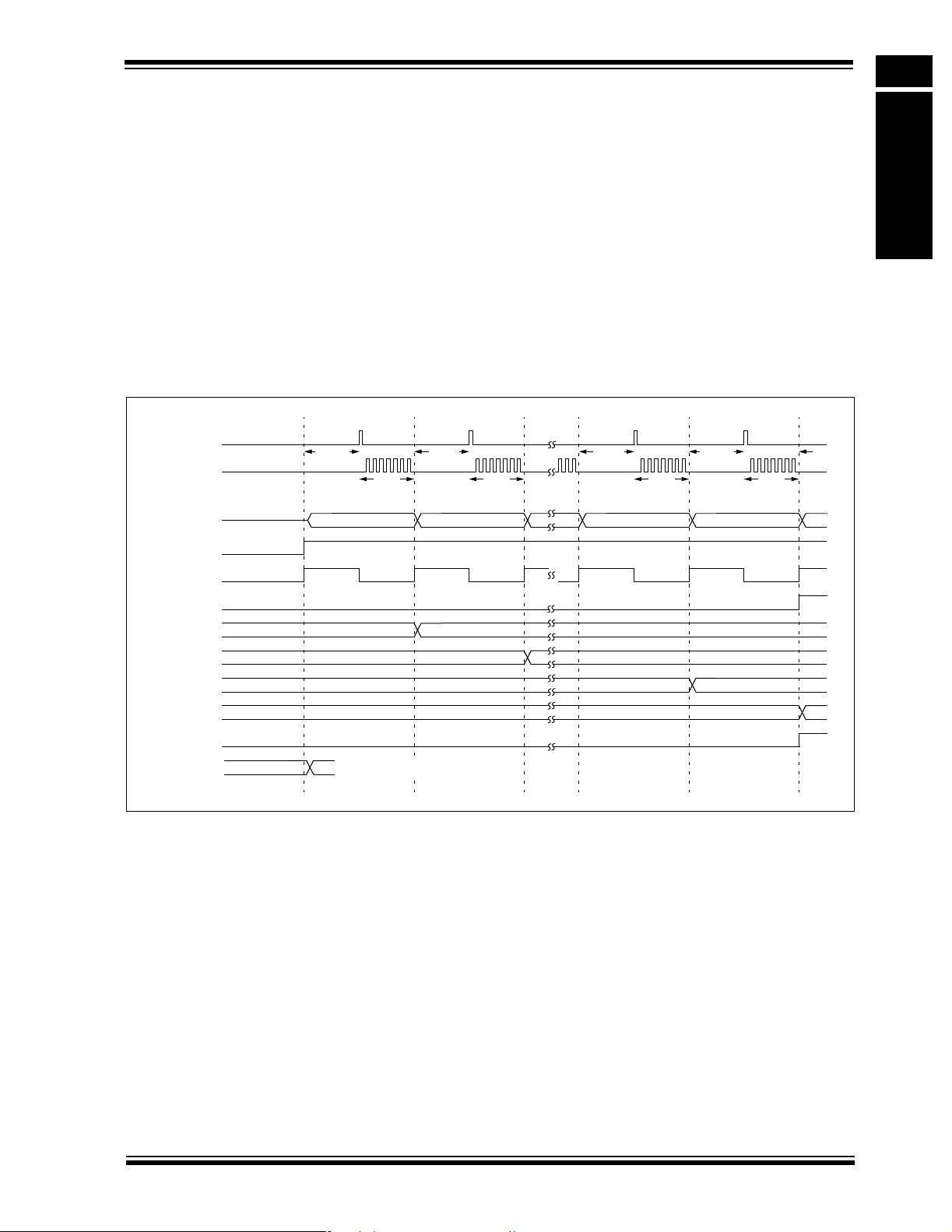
Section 16. Analog-to-Digital Converter (ADC)
ADC
16.14 CONVERSION SEQUENCE EXAMPLES
The following co nfigura tio n examp les s how th e A /D op eratio n in dif fere nt sa mplin g and buf f ering
configurations. In each example, setting the ASAM bit starts automatic sampling. A conversion
trigger ends sampling and starts conversion.
16.14.1 Sampling and Converting a Single Channel Multiple Times
Figure 16-17 and Table 16-2 illustrate a basic configuration of the ADC. In this case, one ADC
input, AN0, is sampl ed by one Sam ple/Hold chan nel, CH0, and con verted. The results ar e stored
in the user-configured DMA buffer, illustrated as Buffer(0) through Buffer(15). This process
repeats 16 times until the buffer is full and then the ADC module generates an interrupt. The
entire process then repeats.
The CHPS bits specify that only Sample/Hold CH0 is active. With ALTS clear, only the MUX A
inputs are active. The CH0SA bits and CH0NA bit are specified (AN0-V
Sample/Hold channel. All other input selection bits are not used.
Figure 16-17: Converting One Channel 16 Times/Interrupt
Conversion
Trigger
ADC Clock
TSAMP
TCO NV
TSAMP
TCO NV
TSAMP
TCONV
16
REF-) as the input to the
TSAMP
TCO NV
Input to CH0
ASAM
SAMP
DONE
Buffer[0]
Buffer[1]
Buffer[2]
Buffer[15]
AD1IF
BSET AD1CON1,ASAM
AN0
Instruction Execution
AN0
AN0
AN0
© 2006 Microchip Technology Inc. DS70183A-page 16-37
Page 38
dsPIC33F Family Reference Manual
Table 16-2: Converting One Channel 16 Times per DMA Interrupt
CONTROL BITS OPERATION SEQUENCE
Sequence Select Sample MUX A Inputs: AN0 -> CH0,
0000
, AMODE = 00, DMAxCNT =
DMA Interrupt on 16th conversion Sample MUX A Inputs: AN0 -> CH0,
Sample Channel CH0 Sample MUX A Inputs: AN0 -> CH0,
SIMSAM = n/a
Not applicable for single channel sample Sample MUX A Inputs: AN0 -> CH0,
BUFM = 0
Single 16-word result buffer Sample MUX A Inputs: AN0 -> CH0,
AL TS = 0
Always use MUX A input select Sample MUX A Inputs: AN0 -> CH0,
MUX A Input Select
CH0SA<4:0> = 00000 Sample MUX A Inputs: AN0 -> CH0,
Select AN0 for CH0+ input
CH0NA = 0 Sample MUX A Inputs: AN0 -> CH0,
Select VREF- for CH0- input
CSCNA = 0 Sample MUX A Inputs: AN0 -> CH0,
No input scan
CSSL<15:0> = n/a Sample MUX A Inputs: AN0 -> CH0,
Scan input select unused
CH123SA = n/a Sample MUX A Inputs: AN0 -> CH0,
Channel CH1, CH2, CH3 + input unused
CH123NA<1:0> = n/a Sample MUX A Inputs: AN0 -> CH0,
Channel CH1, CH2, CH3 – input unused
MUX B Input Select Sample MUX A Inputs: AN0 -> CH0,
CH0SB<4:0> = n/a
Channel CH0+ input unused Sample MUX A Inputs: AN0 -> CH0,
CH0NB = n/a
Channel CH0- input unused Sample MUX A Inputs: AN0 -> CH0,
CH123SB = n/a
Channel CH1, CH2, CH3 + input unused Sample MUX A Inputs: AN0 -> CH0,
CH123NB<1:0> = n/a
Channel CH1, CH2, CH3 – input unused DMA Interrupt
15
write ADC1BUF0 and
write ADC1BUF0 and Generate DMA Reques
write ADC1BUF0 and generate DMA Request
write ADC1BUF0 and
write ADC1BUF0 and
write ADC1B UF0 and generate DMA Request
write ADC1BUF0 and
write ADC1BUF0 and
write ADC1BUF0 and
write ADC1BUF0 and
write ADC1BUF0 and generate DMA Request
write ADC1BUF0 and
write ADC1BUF0 and
write ADC1BUF0 and
write ADC1BUF0 and
write ADC1BUF0 and
Repeat
generate DMA RequestSMPI<3:0> =
generate DMA Request
generate DMA Request
generate DMA Request
generate DMA Request
generate DMA Request
generate DMA Request
generate DMA Request
generate DMA Request
generate DMA Request
generate DMA Request
generate DMA Request
convert CH0,
convert CH0,
tCHPS<1:0> = 00
convert CH0,
convert CH0,
convert CH0,
convert CH0,
convert CH0,
convert CH0,
convert CH0,
convert CH0,
convert CH0,
convert CH0,
convert CH0,
convert CH0,
convert CH0,
Convert CH0,
DMA Buffer @
1st DMA Interrupt
AN0 Sample 1 AN0 Sample 17
AN0 Sample 2 AN0 Sample 18
AN0 Sample 3 AN0 Sample 19
AN0 Sample 4 AN0 Sample 20
AN0 Sample 5 AN0 Sample 21
AN0 Sample 6 AN0 Sample 22
AN0 Sample 7 AN0 Sample 23
AN0 Sample 8 AN0 Sample 24
AN0 Sample 9 AN0 Sample 25
AN0 Sample 10 AN0 Sample 26
AN0 Sample 11 AN0 Sample 27
AN0 Sample 12 AN0 Sample 28
AN0 Sample 13 AN0 Sample 29
AN0 Sample 14 AN0 Sample 30
AN0 Sample 15 AN0 Sample 31
AN0 Sample 16 AN0 Sample 32
DS70183A-page 16-38 © 2006 Microchip Technology Inc.
DMA Buffer @
2nd DMA Interrupt
Page 39

Section 16. Analog-to-Digital Converter (ADC)
ADC
16.14.2 A/D Conversions While Scanning Through All Analog Inputs
Figure 16-18 and Table 16-3 illustrate a typical setup where all available analog input channels
are sampled by one Sample/Hold channel, CH0, and converted. The set Scan Input Selection
(CSCNA) bit (ADxCON2<10>) specifies scanning of the ADC inputs to the CH0 positive input.
Other conditions are similar to those described in Section 16.14.1 “Sampling and Converting
a Single Channel Multiple Times”.
Initially, the AN0 input is sampled by CH0 and converted. The result is stored in the user-configured DMA bu ffer. Then the A N1 inpu t is s ample d and c onver ted. T his p roces s of sc annin g the
inputs repeat s 16 tim es un til the b uffer is full. Then the ADC module generates an inte rrupt. The
entire process then repeats.
Figure 16-18: Scanning Through 16 Inputs /Interrupt
Conversion
Trigger
ADC Clock
TSAMP
TSAMP
TCONV
TCONV
TSAMP
TCONV
16
TSAMP
TCONV
Input to CH0
ASAM
SAMP
DONE
Buffer[0]
Buffer[1]
Buffer[2]
Buffer[15]
AD1IF
BSET AD1CON1,#ASAM
AN0
Instruction Execution
AN1
AN14
AN15
© 2006 Microchip Technology Inc. DS70183A-page 16-39
Page 40

dsPIC33F Family Reference Manual
Table 16-3: Scanning Through 16 Inputs per DMA Interrupt
CONTROL BITS OPERATION SEQUENCE
Sequence Select Sample MUX A Inputs: AN0 -> CH0,
SMPI<3:0> =
CHPS<1:0> = 00 Sample MUX A Inputs: AN2 -> CH0,
SIMSAM = n/a Sample MUX A Inputs: AN3 -> CH0,
BUFM = 0 Sample MUX A Inputs: AN4 -> CH0,
AL TS = 0 Sample MUX A Inputs: AN5 -> CH0,
CH0SB<3:0> = n/a Sample MUX A Inputs: AN13 -> CH0,
CH0NB = n/a Sample MUX A Inputs: AN14 -> CH0,
CH123SB = n/a Sample MUX A Inputs: AN15 -> CH0,
CH123NB<1:0> = n/a Interrupt
1111
, AMODE = 00, DMAxCNT =
DMA Interrupt on 16th conversion Sample MUX A Inputs: AN1 -> CH0,
MUX A Input Select Sample MUX A Inputs: AN6 -> CH0,
Override by CSCNA Sample MUX A Inputs: AN7 -> CH0,
Select V
Channel CH1, CH2, CH3 + input unused Sample MUX A Inputs: AN11 -> CH0,
Channel CH1, CH2, CH3 – input unused Sample MUX A Inputs: AN12 -> CH0,
Channel CH1, CH2, CH3 – input unused Repeat
REF- for CH0- input Sample MUX A Inputs: AN8 -> CH0,
Scan CH0+ Inputs Sample MUX A Inputs: AN9 -> CH0,
16 inputs scanned Sample MUX A Inputs: AN10 -> CH0,
15
write ADC1BUF0,and generate DMA Request
write ADC1BUF0,and generate DMA Request
write ADC1BUF0,and generate DMA RequestSample Channel CH0
write ADC1BUF0,and generate DMA RequestNot applicable for single channel sample
write ADC1BUF0,and generate DMA RequestSingle 16-word result buffer
write ADC1BUF0,and generate DMA RequestAlways use MUX A input select
write ADC1BUF0,and generate DMA RequestCH0SA<4:0> = n/a
write ADC1BUF0,and generate DMA RequestCH0NA = 0
write ADC1BUF0,and generate DMA RequestCSCNA = 1
write ADC1BUF0,and generate DMA RequestCSSL<15:0> = 1111 1111 1111 1111
write ADC1BUF0,and generate DMA RequestCH123SA = n/a
write ADC1BUF0,and generate DMA RequestCH123NA<1:0> = n/a
write ADC1BUF0,and generate DMA RequestMUX B Input Select
write ADC1BUF0,and generate DMA RequestChannel CH0+ input unused
write ADC1BUF0,and generate DMA RequestChannel CH0- input unused
write ADC1BUF0,and generate DMA RequestChannel CH1, CH2, CH3 + input unused
convert CH0,
convert CH0,
convert CH0,
convert CH0,
convert CH0,
convert CH0,
convert CH0,
convert CH0,
convert CH0,
convert CH0,
convert CH0,
convert CH0,
convert CH0,
convert CH0,
convert CH0,
convert CH0,
DMA Buffer @
1st DMA Interrupt
AN0 Sample 1 AN0 Sample 17
AN1 Sample 2 AN1 Sample 18
AN2 Sample 3 AN2 Sample 19
AN3 Sample 4 AN3 Sample 20
AN4 Sample 5 AN4 Sample 21
AN5 Sample 6 AN5 Sample 22
AN6 Sample 7 AN6 Sample 23
AN7 Sample 8 AN7 Sample 24
AN8 Sample 9 AN8 Sample 25
AN9 Sample 10 AN9 Sample 26
AN10 Sample 1 1 AN10 Sample 27
AN11 Sample 12 AN11 Sample 28
AN12 Sample 13 AN12 Sample 29
AN13 Sample 14 AN13 Sample 30
AN14 Sample 15 AN14 Sample 31
AN15 Sample 16 AN15 Sample 32
DS70183A-page 16-40 © 2006 Microchip Technology Inc.
DMA Buffer @
2nd DMA Interrupt
Page 41

Section 16. Analog-to-Digital Converter (ADC)
ADC
16.14.3 Sampling Three Inputs Frequently While Scanning Four Other Inputs
Figure 16-19 and Table 16-4 show how the ADC module could be configured to sample three
inputs frequently using Sample/Hold channels CH1, CH2 and CH3; while four other inputs are
sampled less frequently by scanning them using Sample/Hold channel CH0. In this case, only
MUX A inputs are used, and all four channels are sampled simultaneously. Four different inputs
(AN4, AN5, AN6, AN7) are scanned in CH0, whe reas AN0, AN1 and AN2 are the fixed input s for
CH1, CH2 and CH3, respec tively . Thu s, in every set of 16 s amples, AN0, AN1 an d AN2 are sampled four times, while AN4, AN5, AN6 and AN7 are sampled only once each.
Figure 16-19: Converting Three Inputs, Four Times and Four Inputs, One Time/Interrupt
Conversion
Trigger
ADC Clock
TSAMP
TSAMP
TCONVTCONVTCONVTCONV
CONVTCONVTCONVTCONV TCONVTCONVTCONVTCONV
T
TSAMP
16
Input to CH0
Input to CH1
Input to CH2
Input to CH3
ASAM
SAMP
DONE
Buffer[0]
Buffer[1]
Buffer[2]
Buffer[3]
Buffer[12]
Buffer[13]
Buffer[14]
Buffer[15]
AD1IF
AN4
AN0
AN1
AN2
AN5
AN0
AN1
AN2
AN6
AN0
AN1
AN2
AN7
AN0
AN1
AN2
AN4
AN0
AN1
AN2
© 2006 Microchip Technology Inc. DS70183A-page 16-41
Page 42

dsPIC33F Family Reference Manual
Table 16-4: Converting Three Inputs, Four Times and Four Inputs, One Time per DMA Interrupt
CONTROL BITS OPERATION SEQUENCE
Sequence Select Sample MUX A Inputs:
SMPI<3:0> =
Scan 4 inputs, Interrupt on 16th conversion Convert CH0, wr ite ADC1BU F0, a nd gen erate DM A Reques t
CHPS<1:0> = 1x Convert CH1, write ADC 1BUF0, a nd gen erate DM A Reques t
SIMSAM = 1 Convert CH3, write ADC 1BUF0, a nd gen erate DM A Reques t
BUFM = 0 AN5 -> CH0, AN0 -> CH1, AN1 -> CH2, AN2 -> CH3
AL TS = 0 Convert CH1, write ADC1BUF0, and generat e DMA Req uest
CH0SA<3:0> = n/a Sample MUX A Inputs:
CH0NA = 0 Convert CH0, write ADC 1BUF0, a nd gen erate DM A Reques t
CSCNA = 1 Convert CH2,write ADC1BUF0, and generate DMA Request
CSSL<15:0> = 0000 0000 1111 0000 Sample MUX A Inputs:
CH123SA = 0 Convert CH0, write ADC1BUF0, a nd generat e DMA Req uest
CH123NA<1:0> = 0x Convert CH2, write ADC 1BUF0, a nd gen erate DM A Reques t
CH0SB<3:0> = n/a Repeat
CH0NB = n/a
CH123SB = n/a
CH123NB<1:0> = n/a
0011
, AMODE = 00, DMAxCNT =
Sample Channels CH0, CH1, CH2, CH3 Convert CH2, write ADC1BUF0, and generate DMA Request
Sample all channels simultaneously Sample MUX A Inputs:
Single 16-word result buffer Convert CH0, write ADC1BUF0, and generat e DM A Reques t
Always use MUX A input select Convert CH2, write ADC1BUF0 , and gen erate DM A Reques t
MUX A Input Select Convert CH3, write ADC 1BUF0, a nd gen erate DM A Reques t
Override by CSCNA AN6 -> CH0, AN0 -> CH1, AN1 -> CH2, AN2 -> CH3
Select V
Scan AN4, AN5, AN6, AN7 AN7 -> CH0, AN0 -> CH1, AN1 -> CH2, AN2 -> CH3
CH1+ = AN0, CH2+ = AN1, CH3+ = AN2 Convert CH1, write ADC1BUF0, and generate DMA Request
CH1-, CH2-, CH3- = V
MUX B Input Select Interrupt
Channel CH0+ input unused
Channel CH0- input unused
Channel CH1, CH2, CH3 + input unused
Channel CH1, CH2, CH3 – input unused
REF- for CH0- input Convert CH1, write ADC1BUF0, a nd gen erate DM A Reques t
Scan CH0+ Inputs Convert CH3, write AD C1BUF0 , and generat e DMA Req uest
15
REF- Convert CH3, write ADC1BUF0 , and generat e DMA R eques t
AN4 -> CH0, AN0 -> CH1, AN1 -> CH2, AN2 -> CH3
DMA Buffer @
1st DMA Interrupt
AN4 Sample 1 AN4 Sample 2
AN0 Sample 1 AN0 Sample 5
AN1 Sample 1 AN1 Sample 5
AN2 Sample 1 AN2 Sample 5
AN5 Sample 1 AN5 Sample 2
AN0 Sample 2 AN0 Sample 6
AN1 Sample 2 AN1 Sample 6
AN2 Sample 2 AN2 Sample 6
AN6 Sample 1 AN6 Sample 2
AN0 Sample 3 AN0 Sample 7
AN1 Sample 3 AN1 Sample 7
AN2 Sample 3 AN2 Sample 7
AN7 Sample 1 AN7 Sample 2
AN0 Sample 4 AN0 Sample 8
AN1 Sample 4 AN1 Sample 8
AN2 Sample 4 AN2 Sample 8
DS70183A-page 16-42 © 2006 Microchip Technology Inc.
DMA Buffer @
2nd DMA Interrupt
Page 43

Section 16. Analog-to-Digital Converter (ADC)
ADC
16.14.4 Using Alternating MUX A, MUX B I nput Selections
Figure 16-20 and Table 16-5 demonstrate alternate sampling of the inputs assigned to MUX A
and MUX B. In this example, two channels are enabled to sample simultaneously. Setting the
ALTS bit (ADCxCON2<0>) enables alternating input selections. The first sample uses the MUX
A inputs specifi ed by th e CH 0SA, C H0NA , CH1 23S A an d C H12 3NA b it s . T he nex t s ampl e u se s
the MUX B inputs spec ified b y the CH0SB, CH 0NB, CH123 SB and CH1 23NB bit s. In thi s example, one of the MUX B input specifications uses two analog inputs as a differential source to the
Sample/Hold, sampling (AN3-AN9).
Note that using four Sample/Hold channels without alternating input selections results in the
same number of conversions as this example, using two channels with alternating input selections. However, because the CH1, CH2 and CH3 channels are more limited in the selectivity of
the analog inputs , this example me thod provides more flexibil ity of input sele ction than usi ng four
channels.
Figure 16-20: Converting Two Sets of Two Inputs Using Alternating Input Selections
Conversion
Trigger
ADC Clock
Input to
CH0
Input to
CH1
ASAM
TSAMP
AN1
AN0
TSAMP
TCONVTCONV
AN15
AN3-AN9
TCONVTCONV
TSAMP
AN15
AN3-AN9
TSAMP
TCONVTCONV
AN1
AN0
TCONVTCONV
16
TSAMP
TCONVTCONV
AN15
AN3-AN9
SAMP
DONE
BUFS
Buffer[0]
Buffer[1]
Buffer[2]
Buffer[3]
Buffer[4]
Buffer[5]
Buffer[6]
Buffer[7]
Buffer[8]
ADxIF
Cleared by Software
Cleared
in software
© 2006 Microchip Technology Inc. DS70183A-page 16-43
Page 44

dsPIC33F Family Reference Manual
Table 16-5: Converting Two Sets of Two Inputs Using Alternating Input Selections
CONTROL BITS OPERATION SEQUENCE
Sequence Select Sample MUX A Inputs: AN1 -> CH0, AN0 -> CH1
SMPI<3:0> =
Alt. Sampling, DMA Interrupt on 8th conversion Convert CH1, write ADC1BUF0, and gen erate DM A Reques t
CHPS<1:0> = 01 Sample MUX B Inputs: AN15 -> CH0, (AN3-AN9) -> CH1
SIMSAM = 1 Convert CH1, write ADC 1BUF0, a nd gen erate DM A Reques t
BUFM = 1 Convert CH0, write ADC1BUF0, and gen erate D MA Req uest
AL TS = 1 Sample MUX B Inputs: AN15 -> CH0, (AN3-AN9) -> CH1
CH0SA<3:0> = 0001 Interrupt
CH0NA = 0
CSCNA = 0
CSSL<15:0> = n/a
CH123SA = 0
CH123NA<1:0> = 0x
CH0SB<3:0> = 1111
CH0NB = 0
CH123SB = 1
CH123NB<1:0> = 11
0001
, AMODE = 00, DMAxCNT =
Sample Channels CH0, CH1 Convert CH0, write ADC1BUF0, and generate DMA Request
Sample all channels simultaneously Sample MUX A Inputs: AN1 -> CH0, AN0 -> CH1
Dual 8-word result buffers Convert CH1, write ADC1BUF0 , and generat e DMA Req uest
Alternate MUX A/B input select Convert CH0, write ADC1BUF0 , and generat e DMA Req uest
MUX A Input Select Convert CH1, write ADC 1BUF0, a nd gen erate DM A Reques t
Select AN1 for CH0+ input Repeat
Select V
CH1+ = AN0, CH2+ = AN1, CH3+ = AN2
CH1-, CH2-, CH3- = V
MUX B Input Select
Select AN15 for CH0+ input
Select V
CH1+ = AN3, CH2+ = AN4, CH3+ = AN5
CH1- = AN9, CH2- = AN10, CH3- = AN11
REF- for CH0- input
No input scan
Scan input select unused
REF- for CH0- input
7
REF-
Convert CH0, write ADC 1BUF0, a nd gen erate DM A Reques t
DMA Buffer @
1st DMA Interrupt
AN1 Sample 1 AN1 Sample 3
AN0 Sample 1 AN0 Sample 3
AN15 Sample 1 AN15 Sample 3
(AN3-AN9) Sample 1 (AN3-AN9) Sample 3
AN1 Sample 2 AN1 Sample 4
AN0 Sample 2 AN0 Sample 4
AN15 Sample 2 AN15 Sample 4
(AN3-AN9) Sample 2 (AN3-AN9) Sample 4
DS70183A-page 16-44 © 2006 Microchip Technology Inc.
DMA Buffer @
2nd DMA Interrupt
Page 45

Section 16. Analog-to-Digital Converter (ADC)
ADC
16.14.5 Sampling Eight Inputs Using Simultaneous Sampling
This and the next example demonstrate identical setups with the exception that this example
uses simultaneous sampling (SIMSAM = 1), and the following example uses sequential sampling (SIMSAM = 0). Both examples use alternating inputs and specify differential inputs to the
Sample/Hold.
Figure 16-21 and Table 16-6 demonstrate simultaneous sampling. When converting more than
one channel and selecting simultaneous sampling, the ADC module samples all channels, then
performs the required conversions in sequence. In thi s example, with ASAM set, sampling begins
after the conversions complete.
Figure 16-21: Sampling Eight Inputs Using Simultaneous Sampling
Conversion
Trigger
ADC Clock
TSAMP
TSAMP
T
CONVTCONVTCONVTCONV TCONVTCONVTCONVTCONV TCONVTCONVTCONVTCONV
16
TSAMP
Input to CH0
Input to CH1
Input to CH2
Input to CH3
ASAM
SAMP
DONE
Buffer[0]
Buffer[1]
Buffer[2]
Buffer[3]
Buffer[12]
Buffer[13]
Buffer[14]
Buffer[15]
AD1IF
AN13-AN1
AN0
AN1
AN2
AN14
AN3-AN6
AN4-AN7
AN5-AN8
AN14
AN3-AN6
AN4-AN7
AN5-AN8
AN13-AN1
AN0
AN1
AN2
© 2006 Microchip Technology Inc. DS70183A-page 16-45
Page 46

dsPIC33F Family Reference Manual
Table 16-6: Sampling Eight Inputs Using Simultaneous Sampling
CONTROL BITS OPERATION SEQUENCE
Sequence Select Sample MUX A Inputs:
SMPI<3:0> =
Alt. sampling, DMA interrupt on 16th conversio n Convert CH0, write ADC1BUF0, and gen erate D MA Req uest
CHPS<1:0> = 1x Convert CH1,write ADC1BUF0, and generate DMA Request
SIMSAM = 1 Convert CH3, write ADC 1BUF0, a nd gen erate DM A Reques t
BUFM = 0 AN14 -> CH0,
AL TS = 1 Convert CH0, write ADC1BUF0, and generat e DMA Req uest
CH0SA<3:0> = 1101 Convert CH 3, write ADC1BUF0 , and generat e DMA R equest
CH0NA = 1 (AN13-AN1) -> CH0, AN0 -> CH1, AN1 -> CH2, AN2 -> CH3
CSCNA = 0 Convert CH1, write ADC 1BUF0, a nd gen erate DM A Reques t
CSSL<15:0> = n/a Con vert CH 3, write ADC1BUF0 , and generat e DM A Reques t
CH123SA = 0 AN14 -> CH0,
CH123NA<1:0> = 0x Convert CH0, write ADC 1BUF0, a nd gen erate DM A Reques t
CH0SB<3:0> = 1110 Convert CH 3, write ADC1BUF0 , and generat e DMA R equest
CH0NB = 0 Repeat
CH123SB = 1
CH123NB<1:0> = 10
0001
, AMODE = 00, DMAxCNT =
Sample Channels CH0, CH1, CH2, CH3 Convert CH2, write ADC1BUF0, and generate DMA Request
Sample all channels simultaneously Sample MUX B Inputs:
Single 16-word result buffer (AN3-AN6) -> CH1, (AN4-AN7) -> CH2, (AN5-AN8) -> CH3
Alternate MUX A/MUX B input select Convert CH1, write ADC1BUF0 , and generat e DMA R equest
MUX A Input Select Convert CH2, write ADC 1BUF0, a nd gen erate DM A Reques t
Select AN13 for CH0+ input Sample MUX A Inputs:
Select AN1 for CH0- input Convert CH0, write ADC1BUF0 , and generat e DMA Req uest
No input scan Convert CH2, write ADC1BUF0, and generate DMA Request
Scan input select unused Sample MUX B Inputs:
CH1+ = AN0, CH2+ = AN1, CH3+ = AN2 (AN3-AN6) -> CH1, (AN4-AN7) -> CH2, (AN5-AN8) -> CH3
CH1-, CH2-, CH3- = V
MUX B Input Select Convert CH2, write ADC 1BUF0, a nd gen erate DM A Reques t
Select AN14 for CH0+ input Interrupt
Select V
CH1+ = AN3, CH2+ = AN4, CH3+ = AN5
CH1- = AN6, CH2- = AN7, CH3- = AN8
REF- for CH0- input
15
REF- Convert CH1, write ADC1BUF0 , and generat e DMA R eques t
(AN13-AN1) -> CH0, AN0 -> CH1, AN1 -> CH2, AN2 -> CH3
DMA Buffer @
1st DMA Interrupt
(AN13-AN1) Sample 1 (AN13-AN1) Sample 3
AN0 Sample 1 AN0 Sample 3
AN1 Sample 1 AN1 Sample 3
AN2 Sample 1 AN2 Sample 3
AN14 Sampl e 1 AN14 Sample 3
(AN3-AN6) Sample 1 (AN3-AN6) Sample 3
(AN4-AN7) Sample 1 (AN4-AN7) Sample 3
(AN5-AN8) Sample 1 (AN5-AN8) Sample 3
(AN13-AN1) Sample 1 (AN13-AN1) Sample 4
AN0 Sample 2 AN0 Sample 4
AN1 Sample 2 AN1 Sample 4
AN2 Sample 2 AN2 Sample 4
AN14 Sampl e 2 AN14 Sample 4
(AN3-AN6) Sample 2 (AN3-AN6) Sample 4
(AN4-AN7) Sample 2 (AN4-AN7) Sample 4
(AN5-AN8) Sample 2 (AN5-AN8) Sample 4
DS70183A-page 16-46 © 2006 Microchip Technology Inc.
DMA Buffer @
2nd DMA Interrupt
Page 47

Section 16. Analog-to-Digital Converter (ADC)
ADC
16.14.6 Sampling Eight Inputs Using Sequential Sampling
Figure 16-22 and Table 16-7 de monst rate seque ntial sam pling. When c onverti ng more tha n on e
channel and selecting sequential sampling, the ADC module starts sampling a channel at the
earliest opportunity, then performs the required conversions in sequence. In this example, with
ASAM set, sampling of a channel begins after the conversion of that channel completes.
When ASAM is clear, sampling does not resume after conversion completion but occurs when
the SAMP bit is set.
When utilizing more than one channel, sequential sampling provides more sampling time since
a channel can be sampled while conversion occurs on another.
Figure 16-22: Sampling Eight Inputs Using Sequential Sampling
Conversion
Trigger
ADC Clock
TSAMP
TSAMP
T
CONVTCONVTCONVTCONV TCONVTCONVTCONVTCONV TCONVTCONVTCONVTCONV
16
TSAMP
Input to CH0
Input to CH1
Input to CH2
Input to CH3
ASAM
SAMP
DONE
Buffer[0]
Buffer[1]
Buffer[2]
Buffer[3]
Buffer[12]
Buffer[13]
Buffer[14]
Buffer[15]
AD1IF
AN13-AN1
AN0
AN1
AN2
AN14
AN3-AN6
AN4-AN7
AN5-AN8
AN13-AN1
AN0
AN1
AN2
AN14
AN3-AN6
AN4-AN7
AN5-AN8
AN13-AN1
AN0
AN1
AN2
© 2006 Microchip Technology Inc. DS70183A-page 16-47
Page 48

dsPIC33F Family Reference Manual
Table 16-7: Sampling Eight Inputs Using Sequential Sampling
CONTROL BITS OPERATION SEQUENCE
Sequence Select Sample: (AN13-AN1) -> CH0, convert CH0,
SMPI<3:0> =
0001
, AMODE = 00, DMAxCNT =
15
Alt. sampling, DMA interrupt on 16th sample Sample: AN0 -> CH1, convert CH0,
CHPS<1:0> = 1x write ADC1BUF0, and generate DMA Request
Sample Channels CH0, CH1, CH2, CH3 Sample: AN1 -> CH2, convert CH0,
SIMSAM = 0 write ADC1BUF0, and generate DMA Request
Sample all channels sequentially Sample: AN2 -> CH3, convert CH0,
BUFM = 0 write ADC1BUF0, and generate DMA Request
Single 16-word result buffer Sample: AN14 -> CH0, convert CH0,
AL TS = 1 write ADC1BUF0, and generate DMA Request
Alternate MUX A/B input select Sample: (AN3-AN6) -> CH1, convert CH0,
MUX A Input Select write ADC1BUF0, and generate DMA Request
CH0SA<3:0> = 0110 Sample: (AN4-AN7) -> CH2, convert CH0,
Select AN6 for CH0+ input write ADC1BUF0, and generate DMA Request
CH0NA = 0 Sample: (AN5-AN8) -> CH3, convert CH0,
Select V
REF- for CH0- input write ADC1BUF0, and generate DMA Request
CSCNA = 0 Sample: (AN13-AN1) -> CH0, convert CH0,
No input scan write ADC1BUF0, and generate DMA Request
CSSL<15:0> = n/a Sample: AN0 -> CH1, convert CH0,
Scan input select unused write ADC1BUF0, and generate DMA Request
CH123SA = 0 Sample: AN1 -> CH2, convert CH0,
CH1+ = AN0, CH2+ = AN1, CH3+ = AN2 write ADC1BUF0, and generate DMA Request
CH123NA<1:0> = 0x Sample: AN2 -> CH3, convert CH0,
CH1-, CH2-, CH3- = V
REF- write ADC1BUF0, and generate DMA Request
MUX B Input Select Sample: AN14 -> CH0, convert CH0,
CH0SB<3:0> = 0111 write ADC1BUF0, and generate DMA Request
Select AN7 for CH0+ input Sample: (AN3-AN6) -> CH1, convert CH0,
CH0NB = 0 write ADC1BUF0, and generate DMA Request
Select V
REF- for CH0- input Sample: (AN4-AN7) -> CH2, convert CH0,
CH123SB = 1 write ADC1BUF0, and generate DMA Request
CH1+ = AN3, CH2+ = AN4, CH3+ = AN5 Sample: (AN5-AN8) -> CH3, convert CH0,
CH123NB<1:0> = 0x write ADC1BUF0, and generate DMA Request
CH1-, CH2-, CH3- = V
REF- Interrupt
write ADC1BUF0, and generate DMA Request
Repeat
DMA Buffer @
1st DMA Interrupt
DMA Buffer @
2nd DMA Interrupt
(AN13-AN1) Sample 1 (AN13-AN1) Sample 3
AN0 Sample 1 AN0 Sample 3
AN1 Sample 1 AN1 Sample 3
AN2 Sample 1 AN2 Sample 3
AN14 Sample 1 AN14 Sample 3
(AN3-AN6) Sample 1 (AN3-AN6) Sample 3
(AN4-AN7) Sample 1 (AN4-AN7) Sample 3
(AN5-AN8) Sample 1 (AN5-AN8) Sample 3
(AN13-AN1) Sample 2 (AN13-AN1) Sample 4
AN0 Sample 2 AN0 Sample 4
AN1 Sample 2 AN1 Sample 4
AN2 Sample 2 AN2 Sample 28
AN14 Sample 2 AN14 Sample 4
(AN3-AN6) Sample 2 (AN3-AN6) Sample 4
(AN4-AN7) Sample 2 (AN4-AN7) Sample 4
(AN5-AN8) Sample 2 (AN5-AN8) Sample 4
DS70183A-page 16-48 © 2006 Microchip Technology Inc.
Page 49
Section 16. Analog-to-Digital Converter (ADC)
ADC
16.15 A/D SAMPLING REQUIREMENTS
The analog input model of the 10-bit and 12-bit ADC modes are shown in Figure 16-23 and
Figure 16-24. The tot al samplin g time for the A/D conversion is a function of the internal amplifier
settling time and the holding capacitor charge time.
For the ADC module to meet its specified accuracy, the charge holding capacitor (C
be allowed to fully charg e to th e voltage level on the analog input pin. The analog output source
impedance (RS), the interconnect impedance (RIC) and the internal sampling switch (RSS)
impedance combin e to di rectly affect the time required to charge the cap aci tor C
bined impedance must, therefore, be small enough to fully charge the holding capacitor within
the chosen sample time. To minimize the effects of pin leakage currents on the accuracy of the
ADC module, the maximum recommended source impedance, R
input channel is selected, this sampling function must be completed prior to starting the conversion. The internal holding capacitor will be in a discharged state prior to each sample operation.
A minimum time period should be allowed between conversions for the sample time. For more
details about the minimum sampling time for a device, see the device electrical specifications.
Figure 16-23: Analog Input Model (10-bit Mode)
16
HOLD) must
HOLD. The com-
S, is 200Ω. After the analog
VDD
V
ANx
Rs
VA
Legend: CPIN
Note: CPIN value depends on device package and is not tested. Effect of CPIN negligible if Rs ≤ 500Ω.
CPIN
VT
I leakage
R
IC
RSS
CHOLD
= input capacitance
= threshold voltage
= leakage current at the pin due to
various junctions
= interconnect resistance
= sampling switch resistance
= Sample/Hold capacitance (from DAC)
T = 0.6V
VT = 0.6V
R
IC ≤ 250Ω
I leakage
± 500 nA
Sampling
Switch
SS
R
SS ≤ 3 kΩ
R
CHOLD
= DAC capacitance
= 4.4 pF
SS
V
Figure 16-24: Analog Input Model (12-bit Mode)
VA
Rs
ANx
CPIN
VDD
V
T = 0.6V
VT = 0.6V
IC ≤ 250Ω
R
I leakage
± 500 nA
Sampling
Switch
SS
R
SS ≤ 3 kΩ
R
CHOLD
= DAC capacitance
= 18 pF
SS
V
Legend: CPIN
VT
I leakage
R
RSS
CHOLD
Note: CPIN value depends on device package and is not tested. Effect of CPIN negligible if Rs ≤ 5 kΩ.
= input capacitance
= threshold voltage
= leakage current at the pin due to
various junctions
= interconnect resistance
IC
= sampling switch resistance
= Sample/Hold capacitance (from DAC)
© 2006 Microchip Technology Inc. DS70183A-page 16-49
Page 50

dsPIC33F Family Reference Manual
16.16 READING THE ADC RESULT BUFFER
The RAM is 10-bits or 12-bits wide, but the data is automatically formatted to one of four selectable formats when the buffer is read. The FORM<1:0> bits (ADCON1<9:8>) select the format.
The formatting hardware provides a 16-bit result on the data bus for all of the data formats.
Figure 16-25 and Figure 16-26 show the data output formats that can be selected using the
FORM<1:0> control bits.
Figure 16-25: A/D Output Data Formats (10-bit Mode)
RAM Contents: d09 d08 d07 d06 d05 d04 d03 d02 d01 d00
Read to Bus:
Integer 000000d09d08d07d06d05d04d03d02d01d00
Signed Integer d09 d09 d09 d09 d09 d09 d09 d08 d07 d06 d05 d04 d03 d02 d01 d00
Fractional (1.15) d09d08d07d06d05d04d03d02d01d00000000
Signed Fractional (1.15) d09d08d07d06d05d04d03d02d01d00000000
Figure 16-26: A/D Output Data Formats (12-bit Mode)
RAM Contents: d11 d10 d09 d08 d07 d06 d05 d04 d03 d02 d01 d00
Read to Bus:
Integer 0 0 0 0 d11 d10 d09 d08 d07 d06 d05 d04 d03 d02 d01 d00
Signed Integer d11 d11 d11 d11 d11 d10 d09 d08 d07 d06 d05 d04 d03 d02 d01 d00
Fractional d11d10d09d08d07d06d05d04d03d02d01d000000
Signed Fractional (1.15) d11d10d09d08d07d04d03d02d01d00d01d000000
DS70183A-page 16-50 © 2006 Microchip Technology Inc.
Page 51

Section 16. Analog-to-Digital Converter (ADC)
ADC
Table 16-8: Numerical Equivalents of Various Result Codes (10-bit Mode)
VIN/VREF
1023/1024
1022/1024
513/1024
512/1024
511/1024
1/1024
0/1024
10-bit
Output Code
11 1111
1111
11 1111
1110
10 0000
0001
10 0000
0000
01 1111
1111
00 0000
0001
00 0000
0000
16-bit Integer Format
0000 0011 1111
1111
= 1023
0000 0011 1111
1110
= 1022
0000 0010 0000
0001
= 513
0000 0010 0000
0000
= 512
0000 0001 1111
1111
= 511
0000 0000 0000
0001
= 1
0000 0000 0000
0000
= 0
16-bit Signed
Integer Format
0000 0001 1111
1111
= 511
0000 0001 1111
1110
= 5 10
• • •
0000 0000 0000
0001
= 1
0000 0000 0000
0000
= 0
1111 1111 1111
1111
= -1
• • •
1111 1110 0000
0001
= -511
1111 1110 0000
0000
= -512
16-bit Fractional Format
1111 1111 1100
= 0.999
1111 1111 1000
= 0.998
1000 0000 0100
= 0.501
1000 0000 0000
= 0.500
0111 1111 1100
= .499
0000 0000 0100
= 0.001
0000 0000 0000
= 0.000
0000
0000
0000
0000
0000
0000
0000
16
16-bit Signed
Fractional Format
0111 1111 1100
0000
= 0.499
0111 1111 1000
0000
= 0.498
0 000 0000 0100
0000
= 0.001
0000 0000 0000
0000
= 0.000
1111 1111 1100
0000
= -0.001
1000 0000 0100
0000
= -0.499
1000 0000 0000
0000
= -0.500
Table 16-9: Numerical Equivalents of Various Result Codes (12-bit Mode)
VIN/VREF
4095/4096
4094/4096
2049/4096
2048/4096
2047/4096
1/4096
0/4096
12-bit
Output Code
1111 1111
1111
1111 1111
1110
1000 0000
0001
1000 0000
0000
0111 1111
1111
0000 0000
0001
0000 0000
0000
16-bit Unsigned
Integer Format
0000 1111 1111
1111
= 4095
0000 1111 1111
1110
= 4094
0000 1000 0000
0001
= 2049
0000 1000 0000
0000
= 2048
0000 0111 1111
1111
= 2047
0000 0000 0000
0001
= 1
0000 0000 0000
0000
= 0
16-bit Signed
Integer Format
0000 0111 1111
1111
= 2047
0000 0111 1111
1110
= 2046
• • •
0000 0000 0000
0001
= 1
0000 0000 0000
0000
= 0
1111 1111 1111
1111
= -1
• • •
1111 1000 0000
0001
= -2047
1111 1000 0000
0000
= -2048
16-bit Unsigned
Fractional Format
1111 1111 1111
= 0.9998
1111 1111 1110
= 0.9995
1000 0000 0001
= 0.5002
1000 0000 0000
= 0.500
0111 1111 1111
= 0.4998
0000 0000 0001
= 0.0002
0000 0000 0000
= 0.000
0000
0000
0000
0000
0000
0000
0000
16-bit Signed
Fractional Format
0111 1111 1111
0000
= 0.9995
0111 1111 1110
0000
= 0.9990
0000 0000 0001
0000
= 0.0005
0000 0000 0000
0000
= 0.000
1111 1111 1111
0000
= -0.0005
1000 0000 0001
0000
= -0.9995
1000 0000 0000
0000
= -1.000
© 2006 Microchip Technology Inc. DS70183A-page 16-51
Page 52

dsPIC33F Family Reference Manual
16.17 TRANSFER FUNCTION (10-BIT MODE)
The ideal transfer function of the ADC module is shown in Figure 16-27. The difference of the
input voltages, (V
• The first code transition (A) occurs when the input voltage is (V
LSb.
•The 00 0000 0001 code is centered at (V
•The 10 0000 0000 code is centered at (512*(V
• An input voltage less than (1*(VREFH – VREFL)/2048) converts as 00 0000 0000 (D).
• An input greater than (2045*(VREFH – VREFL)/2048) converts as 11 1111 1111 (E).
Figure 16-27: ADC Module Transfer Function (10-bit Mode)
Output
Code
INH – VINL), is compared to the reference, (VREFH – VREFL).
REFH – VREFL/2048) or 0.5
REFH – VREFL/1024) or 1.0 LSb (B).
REFH – VREFL)/10 24) (C).
11 1111 1111 (= 1023)
11 1111 1110 (= 1022)
10 0000 0011 (= 515)
10 0000 0010 (= 514)
10 0000 0001 (= 513)
10 0000 0000 (= 512)
01 1111 1111 (= 511)
01 1111 1110 (= 510)
01 1111 1101 (= 509)
00 0000 0001 (= 1)
00 0000 0000 (= 0)
(A)
V
REFL
(B)
VREFL +
(D)
VREFH – VREFL
1024
VREFL +
(C)
512*(VREFH – VREFL)
1024
VREFL +
(E)
1023*(V
REFH – VREFL)
1024
(VINH – VINL)
VREFH
DS70183A-page 16-52 © 2006 Microchip Technology Inc.
Page 53

Section 16. Analog-to-Digital Converter (ADC)
ADC
16.18 TRANSFER FUNCTION (12-BIT MODE)
The ideal transfer fun ct ion of th e AD C is sh ow n in Fig ure16-27. The difference of the input vol t ages (V
• The first code transition (A) occurs when the input voltage is (V
•The 00 0000 0001 code is centered at (V
•The 10 0000 0000 code is centered at (2048*(V
• An input voltage less than (1*(VREFH – VREFL)/8192) converts as 00 0000 0000 (D).
• An input greater than (8192*(VREFH – VREFL)/8192) converts as 11 1111 1111 (E).
Figure 16-28: A/D Transfer Function (12-bit Mode)
Output
Code
1111 1111 1111 (= 4095)
1111 1111 1110 (= 4094)
1000 0000 0011 (= 2051)
1000 0000 0010 (= 2050)
1000 0000 0001 (= 2049)
1000 0000 0000 (= 2048)
0111 1111 1111 (= 2047)
0111 1111 1110 (= 2046)
0111 1111 1101 (= 2045)
INH – VINL) is compared to the reference (VREFH – VREFL).
LSb.
16
REFH – VREFL/8192) or 0.5
REFH – VREFL/4096) or 1.0 LSb (B).
REFH – VREFL)/4096) (C).
(E)
(C)
0000 0000 0001 (= 1)
0000 0000 0000 (= 0)
(A)
V
REFL
V
REFL
(B)
(D)
V
2048*(V
REFH
– V
REFL
V
REFH
– V
4096
REFL
V
REFL
+
4096
+
)
REFH
(V
INH
– V
INL
)
© 2006 Microchip Technology Inc. DS70183A-page 16-53
Page 54

dsPIC33F Family Reference Manual
16.19 ADC ACCURACY/ERROR
Refer to Section 16.26 “Related Application Notes” for a list of documents that discuss ADC
accuracy.
16.20 CONNECTION CONSIDERATIONS
Since the analog inputs employ ESD protection, they have diodes to VDD and VSS. As a result,
the analog input must be betwee n V
than 0.3 V (either directio n), o ne of the diodes becomes forward biased, and it ma y da ma ge th e
device if the input current specification is exceeded.
An external RC filter is sometimes added for anti-aliasing of the input signal. The R component
should be selected to ensure that the sampling time requirements are satisfied. Any external
components conn ected (via hi gh-impedance) to an analog inpu t pin (capac itor , zene r diode, etc.)
should have very little leakage current at the pin.
16.21 CODE EXAMPLES
Two code examples that demonstrate typical ADC usage scenarios are described here:
16.21.1 Channel Scanning Using DMA
Example 16-4 con figure s a DM A cha nnel f or stor ing 32 ADC r esu lts in the Sca tter/Ga ther m ode.
The ADC is set up to scan four analog inputs (AN0, AN1, AN2, AN3), thereby providing eight
samples of each input in the DMA buffer.
DD and VSS. If the inpu t voltage ex ceeds this ra nge by greater
16.21.2 Alternate Sampling Using DMA
Example 16-5 performs alternate sampling of two analog inputs (AN4, AN5) and stores the
results in a 32-word DMA buffer using the Scatter/Gather mode.
DS70183A-page 16-54 © 2006 Microchip Technology Inc.
Page 55

Section 16. Analog-to-Digital Converter (ADC)
ADC
Example 16-4: Code for Channel Scanning Using DMA
/**********************************************************************
* © 2005 Microchip Technology Inc.
*
* FileName: adcDrv1.c
* Dependencies: Header (.h) files if applicable, see below
* Processor: dsPIC33Fxxxx
* Compiler: MPLAB® C30 v2.01.00 or higher
*
* SOFTWARE LICENSE AGREEMENT:
* Microchip Technology Inc. (“Microchip”) licenses this software to you solely for use with
* Microchip dsPIC® digital signal controller products. The software is owned by Microchip
* and is protected under applicable copyright laws. All rights reserved.
*
* SOFTWARE IS PROVIDED “AS IS.” MICROCHIP EXPRESSLY DISCLAIMS ANY WARRANTY OF ANY KIND,
* WHETHER EXPRESS OR IMPLIED, INCLUDING BUT NOT LIMITED TO, THE IMPLIED WARRANTIES OF
* MERCHANTABILITY, FITNESS FOR A PARTICULAR PURPOSE, OR NON-INFRINGEMENT. IN NO EVENT SHALL
* MICROCHIP BE LIABLE FOR ANY INCIDENTAL, SPECIAL, INDIRECT OR CONSEQUENTIAL DAMAGES, LOST
* PROFITS OR LOST DATA, HARM TO YOUR EQUIPMENT, COST OF PROCUREMENT OF SUBSTITUTE GOODS,
* TECHNOLOGY OR SERVICES, ANY CLAIMS BY THIRD PARTIES (INCLUDING BUT NOT LIMITED TO ANY
* DEFENSE THEREOF), ANY CLAIMS FOR INDEMNITY OR CONTRIBUTION, OR OTHER SIMILAR COSTS.
*
********************************************************************************************/
#if defined(__dsPIC33F__)
#include "p33fxxxx.h"
#elif defined(__PIC24H__)
#include "p24hxxxx.h"
#endif
16
void ProcessADCSamples(unsigned int * AdcBuffer);
/*==========================================================================================
ADC Initialization for Channel Scan
===========================================================================================*/
void initAdc1(void)
{
AD1CON1bits.FORM = 3; // Data Output Format: Signed Fraction (Q15 format)
AD1CON1bits.SSRC = 2; // Sample Clock Source: GP Timer starts conversion
AD1CON1bits.ASAM = 1; //
AD1CON1bits.AD12B = 0; // 10-bit ADC operation
AD1CON1bits.SIMSAM = 0; // Samples multiple channels individually in sequence
AD1CON2bits.BUFM = 0;
AD1CON2bits.CSCNA = 1; // Scan Input Selections for CH0+ during Sample A bit
AD1CON2bits.CHPS = 0; // Converts CH0
AD1CON3bits.ADRC = 0; // ADC Clock is derived from Systems Clock
AD1CON3bits.ADCS = 63; // ADC Conversion Clock
//AD1CHS0: A/D Input Select Register
AD1CHS0bits.CH0SA = 0; // MUXA +ve input selection (AIN0) for CH0
AD1CHS0bits.CH0NA = 0; // MUXA -ve input selection (Vref-) for CH0
ADC Sample Control: Sampling begins immediately after conversion
© 2006 Microchip Technology Inc. DS70183A-page 16-55
Page 56

dsPIC33F Family Reference Manual
Example 16-4: Code for Channel Scanning Using DMA (Continued)
//AD1CHS123: A/D Input Select Register
AD1CHS123bits.CH123SA = 0; // MUXA +ve input selection (AIN0) for CH1
AD1CHS123bits.CH123NA = 0; // MUXA -ve input selection (Vref-) for CH1
//AD1CSSH/AD1CSSL: A/D Input Scan Selection Register
AD1CSSH = 0x0000;
AD1CSSL = 0x000F; // Scan AIN0, AIN1, AIN2, AIN3 inputs
AD1CON1bits.ADDMABM = 0; // DMA buffers are built in scatter/gather mode
AD1CON2bits.SMPI = 3; // 4 ADC buffers
AD1CON4bits.DMABL = 3; // Each buffer contains 8 words
IFS0bits.AD1IF = 0; // Clear the A/D interrupt flag bit
IEC0bits.AD1IE = 0; // Do Not Enable A/D interrupt
AD1CON1bits.ADON = 1; // Turn on the A/D converter
}
/*======================================================================================
Timer 3 is setup to time-out every 125 microseconds (8Khz Rate). As a result, the module
will stop sampling and trigger a conversion on every Timer3 time-out, i.e., Ts=125us.
=======================================================================================*/
void initTmr3()
{
TMR3 = 0x0000;
PR3 = 4999; // Trigger ADC1 every 125usec
IFS0bits.T3IF = 0; // Clear Timer 3 interrupt
IEC0bits.T3IE = 0; // Disable Timer 3 interrupt
T3CONbits.TON = 1; //Start Timer 3
}
// Linker will allocate these buffers from the bottom of DMA RAM.
struct
{
unsigned int Adc1Ch0[8];
unsigned int Adc1Ch1[8];
unsigned int Adc1Ch2[8];
unsigned int Adc1Ch3[8];
} BufferA __attribute__((space(dma)));
struct
{
unsigned int Adc1Ch0[8];
unsigned int Adc1Ch1[8];
unsigned int Adc1Ch2[8];
unsigned int Adc1Ch3[8];
} BufferB __attribute__((space(dma)));;
// DMA0 configuration
// Direction: Read from peripheral address 0-x300 (ADC1BUF0) and write to DMA RAM
// AMODE: Peripheral Indirect Addressing Mode
// MODE: Continuous, Ping-Pong Mode
// IRQ: ADC Interrupt
DS70183A-page 16-56 © 2006 Microchip Technology Inc.
Page 57

Section 16. Analog-to-Digital Converter (ADC)
ADC
Example 16-4: Code for Channel Scanning Using DMA (Continued)
void initDma0(void)
{
DMA0CONbits.AMODE = 2; // Configure DMA for Peripheral indirect mode
DMA0CONbits.MODE = 2; // Configure DMA for Continuous Ping-Pong mode
DMA0PAD = 0x0300; // Point DMA to ADC1BUF0
DMA0CNT = 31; // 32 DMA request (4 buffers, each with 8 words)
DMA0REQ = 13; // Select ADC1 as DMA Request source
DMA0STA = __builtin_dmaoffset(&BufferA);
DMA0STB = __builtin_dmaoffset(&BufferB);
IFS0bits.DMA0IF = 0; //Clear the DMA interrupt flag bit
IEC0bits.DMA0IE = 1; //Set the DMA interrupt enable bit
DMA0CONbits.CHEN=1; // Enable DMA
}
/*========================================================================================
_DMA0Interrupt(): ISR name is chosen from the device linker script.
========================================================================================*/
16
unsigned int DmaBuffer = 0;
void __attribute__((__interrupt__)) _DMA0Interrupt(void)
{
if(DmaBuffer == 0)
{
ProcessADCSamples(BufferA.Adc1Ch0);
ProcessADCSamples(BufferA.Adc1Ch1);
ProcessADCSamples(BufferA.Adc1Ch2);
ProcessADCSamples(BufferA.Adc1Ch3);
}
else
{
ProcessADCSamples(BufferB.Adc1Ch0);
ProcessADCSamples(BufferB.Adc1Ch1);
ProcessADCSamples(BufferB.Adc1Ch2);
ProcessADCSamples(BufferB.Adc1Ch3);
}
DmaBuffer ^= 1;
IFS0bits.DMA0IF = 0; //Clear the DMA0 Interrupt Flag
}
void ProcessADCSamples(unsigned int * AdcBuffer)
{
/* Do something with ADC Samples */
}
© 2006 Microchip Technology Inc. DS70183A-page 16-57
Page 58

dsPIC33F Family Reference Manual
Example 16-5: Code for Alternate Sampling Using DMA
/********************************************************************************************
* © 2005 Microchip Technology Inc.
*
* FileName: adcDrv1.c
* Dependencies: Header (.h) files if applicable, see below
* Processor: dsPIC33Fxxxx
* Compiler: MPLAB® C30 v2.01.00 or higher
*
* SOFTWARE LICENSE AGREEMENT:
* Microchip Technology Inc. (“Microchip”) licenses this software to you solely for use with
* Microchip dsPIC® digital signal controller products. The software is owned by Microchip
* and is protected under applicable copyright laws. All rights reserved.
* *
* SOFTWARE IS PROVIDED “AS IS.” MICROCHIP EXPRESSLY DISCLAIMS ANY WARRANTY OF ANY KIND,
* WHETHER EXPRESS OR IMPLIED, INCLUDING BUT NOT LIMITED TO, THE IMPLIED WARRANTIES OF
* MERCHANTABILITY, FITNESS FOR A PARTICULAR PURPOSE, OR NON-INFRINGEMENT. IN NO EVENT
* SHALL MICROCHIP BE LIABLE FOR ANY INCIDENTAL, SPECIAL, INDIRECT OR CONSEQUENTIAL DAMAGES,
* LOST PROFITS OR LOST DATA, HARM TO YOUR EQUIPMENT, COST OF PROCUREMENT OF SUBSTITUTE GOODS,
* TECHNOLOGY OR SERVICES, ANY CLAIMS BY THIRD PARTIES (INCLUDING BUT NOT LIMITED TO
* ANY DEFENSE THEREOF), ANY CLAIMS FOR INDEMNITY OR CONTRIBUTION, OR OTHER SIMILAR COSTS.
*
*********************************************************************************************/
#if defined(__dsPIC33F__)
#include "p33fxxxx.h"
#elif defined(__PIC24H__)
#include "p24hxxxx.h"
#endif
#include "adcDrv1.h"
#include "tglPin.h"
// Define Message Buffer Length for ECAN1/ECAN2
#define MAX_CHNUM 5
#define SAMP_BUFF_SIZE 16 // Size of the input buffer per analog input
// Number of locations for ADC buffer = 2 (AN4 and AN5) x 16 = 32 words
// Align the buffer to 32words or 64 bytes. This is needed for peripheral indirect mode
int BufferA[MAX_CHNUM+1][SAMP_BUFF_SIZE] __attribute__((space(dma),aligned(64)));
int BufferB[MAX_CHNUM+1][SAMP_BUFF_SIZE] __attribute__((space(dma),aligned(64)));
void ProcessADCSamples(int * AdcBuffer);
/*=============================================================================
ADC Initialisation for Channel Scan
=============================================================================*/
void initAdc1(void)
{
AD1CON1bits.FORM = 3; // Data Output Format: Signed Fraction (Q15 format)
AD1CON1bits.SSRC = 2; // Sample Clock Source: GP Timer starts conversion
AD1CON1bits.ASAM = 1; //
AD1CON1bits.AD12B = 0; // 10-bit ADC operation
AD1CON2bits.ALTS=1; // Alternate Input Sample Mode Select Bit
AD1CON2bits.CHPS = 0; // Converts CH0
// Highest Analog input number enabled for alternate sampling
ADC Sample Control: Sampling begins immediately after conversion
DS70183A-page 16-58 © 2006 Microchip Technology Inc.
Page 59

Section 16. Analog-to-Digital Converter (ADC)
ADC
Example 16-5: Code for Alternate Sampling Using DMA (Continued)
16
AD1CON3bits.ADRC = 0; // ADC Clock is derived from Systems Clock
AD1CON3bits.ADCS = 63;
AD1CON1bits.ADDMABM = 0; // DMA buffers are built in scatter/gather mode
AD1CON2bits.SMPI = 1; // SMPI Must be programmed to 1 for this case
AD1CON4bits.DMABL = 4; // Each buffer contains 16 words
//AD1CHS0: A/D Input Select Register
AD1CHS0bits.CH0SA=4; // MUXA +ve input selection (AIN4) for CH0
AD1CHS0bits.CH0NA=0; // MUXA -ve input selection (Vref-) for CH0
AD1CHS0bits.CH0SB=5; // MUXB +ve input selection (AIN5) for CH0
AD1CHS0bits.CH0NB=0; // MUXB -ve input selection (Vref-) for CH0
//AD1PCFGH/AD1PCFGL: Port Configuration Register
AD1PCFGL=0xFFFF;
AD1PCFGH=0xFFFF;
AD1PCFGLbits.PCFG4 = 0; // AN4 as Analog Input
AD1PCFGLbits.PCFG5 = 0; // AN5 as Analog Input
IFS0bits.AD1IF = 0; // Clear the A/D interrupt flag bit
IEC0bits.AD1IE = 0; // Do Not Enable A/D interrupt
AD1CON1bits.ADON = 1; // Turn on the A/D converter
tglPinInit();
}
// ADC Conversion Clock Tad=Tcy*(ADCS+1)=(1/40M)*64 = 1.6us(625Khz)
// ADC Conversion Time for 10-bit Tc=12*Tab = 19.2us
/*========================================================================================
Timer 3 is set up to time-out every 125 microseconds (8Khz Rate). As a result, the module
will stop sampling and trigger a conversion on every Timer3 time-out, i.e., Ts=125us.
==========================================================================================*/
void initTmr3()
{
TMR3 = 0x0000;
PR3 = 4999;
IFS0bits.T3IF = 0;
IEC0bits.T3IE = 0;
//Start Timer 3
T3CONbits.TON = 1;
}
// DMA0 configuration
// Direction: Read from peripheral address 0-x300 (ADC1BUF0) and write to DMA RAM
// AMODE: Peripheral Indirect Addressing Mode
// MODE: Continuous, Ping-Pong Mode
// IRQ: ADC Interrupt
// ADC stores results stored alternatively between DMA_BASE[0]/DMA_BASE[16] on every 16th DMA request
void initDma0(void)
{
DMA0CONbits.AMODE = 2; // Configure DMA for Peripheral indirect mode
DMA0CONbits.MODE = 2; // Configure DMA for Continuous Ping-Pong mode
DMA0PAD=(int)&ADC1BUF0;
DMA0CNT = (SAMP_BUFF_SIZE*2)-1;
© 2006 Microchip Technology Inc. DS70183A-page 16-59
Page 60

dsPIC33F Family Reference Manual
Example 16-5: Code for Alternate Sampling Using DMA (Continued)
DMA0REQ=13;
DMA0STA = __builtin_dmaoffset(&BufferA[0][0]);
DMA0STB = __builtin_dmaoffset(&BufferB[0][0]);
IFS0bits.DMA0IF = 0; //Clear the DMA interrupt flag bit
IEC0bits.DMA0IE = 1; //Set the DMA interrupt enable bit
DMA0CONbits.CHEN=1;
}
/*=======================================================================================
_DMA0Interrupt(): ISR name is chosen from the device linker script.
=======================================================================================*/
unsigned int DmaBuffer = 0;
void __attribute__((__interrupt__)) _DMA0Interrupt(void)
{
if(DmaBuffer==0) {
ProcessADCSamples(&BufferA[4][0]);
ProcessADCSamples(&BufferA[5][0]);
} else {
ProcessADCSamples(&BufferB[4][0]);
ProcessADCSamples(&BufferB[5][0]);
}
DmaBuffer ^= 1;
tglPin(); // Toggle PORTA, BIT0
IFS0bits.DMA0IF = 0;//Clear the DMA0 Interrupt Flag
}
void ProcessADCSamples(int * AdcBuffer)
{
/* Do something with ADC Samples */
}
DS70183A-page 16-60 © 2006 Microchip Technology Inc.
Page 61

Section 16. Analog-to-Digital Converter (ADC)
ADC
16.22 OPERATION DURING SLEEP AND IDLE MODES
Sleep and Idle modes are useful for minimizing conversion noise because the digital activity of
the CPU, buses and other periphera ls is minimized.
16.22.1 CPU Sleep Mode without RC A/D Clock
When the device enters Sleep mode, all clock sources to the ADC module are shut down and
stay at logic ‘0’.
If Sleep occurs in the middle of a conversion, the conversion is aborted unless the ADC is
clocked from its internal RC clock generator. The converter does not resume a partially completed conversion on exiting from Sleep mode.
Register contents are not affected by the device entering or leaving Sleep mode.
16.22.2 CPU Sleep Mode with RC A/D Clock
The ADC module can o perate during Sl eep mode if the A/D clock source is s et to the intern al A/D
RC oscillator (ADRC = 1). This eliminates digit al sw it ch ing noi se from the conversio n. W hen the
conversion is com pleted, the DONE bit is set an d th e result is load ed into the AD C Res ult buf fer,
ADCBUF.
If the ADC interrupt is enabled (ADxIE = 1), the device wakes up from Sleep when the ADC
interrupt occurs. Program execution resumes at the ADC Interrupt Service Routine if the ADC
interrupt is greater than the current CPU priority. Otherwise, execution continues from the
instruction after the PWRSAV instruction that placed the device in Sleep mode.
If the ADC interrupt is not enabled, th e ADC module is turned of f, although the ADON bit remains
set.
To minimize the effects of digital noise on the ADC module operation, the user should select a
conversion trigger source that ensures the A/D conversion will take place in Sleep mode. The
automatic conversion trigger option can be used for sampling and conversion in Sleep
(SSRC<2:0> = 111). To use the automatic conversion o ption, the ADON bit shou ld b e set i n the
instruction before the PWRSAV instruction.
16
Note: For the ADC module to operate in Sleep, the ADC clock source must be set to RC
(ADRC = 1).
16.22.3 ADC Operation During CPU Idle Mode
For the A/D conversion , the ADSIDL bit (ADxCON1<13>) selec ts if the ADC module stop s or continues on Idle. If ADSIDL = 0, the ADC module continues normal operation when the device
enters Idle mode. If the ADC interrupt is enabled (ADxIE = 1), the device wakes up from Idle
mode when the ADC inte rrupt occurs. Program exe cu tio n re su mes a t th e ADC In terru pt Serv ice
Routine if the ADC interrupt is greater than the current CPU priority. Otherwise, execution continues from the instruction after the PWRSAV instruction that placed the device in Idle mode.
If ADSIDL = 1, the ADC module stops in Idle. If the device enters Idle mode in the middle of a
conversion, the conversion is aborted. The converter does not resume a partially completed
conversion on exiting from Idle mode.
© 2006 Microchip Technology Inc. DS70183A-page 16-61
Page 62

dsPIC33F Family Reference Manual
16.23 EFFECTS OF A RESET
A device Reset forces all reg isters to the ir Reset st ate. Th is forces the ADC m odule to be turned
off and any conv ersio n in p rogress to be aborted . All pi ns tha t are m ultipl exed wi th analog input s
are configured as analog inputs. The corresponding TRIS bits are set.
The value in the ADCxBUF0 register is not initialized during a Power-on Reset and contain
unknown data.
16.24 SPECIAL FUNCTION REGISTERS ASSOCIATED WITH THE ADC
The following table lists dsPIC33F ADC Spe cial Function regis ters, including th eir addresses and
formats. All unimplemented registers and/or bits within a register are read as zeros.
DS70183A-page 16-62 © 2006 Microchip Technology Inc.
Page 63

© 2006 Microchip Technology Inc. DS70183A-page 16-63
ADC
Table 16-10: ADC Register Map
File Name ADR Bit 15 Bit 14
INTCON1
INTCON2
IFS0
IFS1
IEC0
IEC1
IPC3
IPC5
ADC1BUF0
AD1CON1
AD1CON2
AD1CON3
AD1CHS123
AD1CHS0
AD1PCFGH
AD1PCFGL
AD1CSSH
AD1CSSL
AD1CON4
ADC2BUF0
AD2CON1
AD2CON2
AD2CON3
AD2CHS123
AD2CHS0
AD2PCFGL
AD2CSSL
AD2CON4
0080
NSTDIS OV AERR OVBERR COVAERR COVBERR
0082
ALTIVT DISI — — —
0084
0086
0094
0096
00AA
00AE
0300
0320
0322
0324
0326
0328
032A
032C
032E
0330
0332
0340
0360
0362
0364
0366
0368
036C
0370
0372
— DMA1IF AD1IF U1TXIF U1RXIF
U2TXIF U2RXIF INT2IF T5IF T4IF
— DMA1IE AD1IE U1TXIE U1RXIE
U2TXIE U2RXIE INT2IE T5IE T4IE
— — — — —
— IC8IP<2:0> —
ADON — ADSIDL ADDMABM —
VCFG<2:0> — —
ADRC — — SAMC<4:0> — — ADCS<5:0>
— — — — —
CH0NB — — CH0SB<4:0> CH0NA — — CH0SA<4:0>
PCFG31 PCFG30 PCFG29 PCFG28 PCFG27 PCFG26 PCFG25
PCFG15 PCFG14 PCFG13 PCFG12 PCFG11 PCFG10
CSS31 CSS30 CSS29 CSS28 CSS27
CSS15 CSS14 CSS13 CSS12 CSS11
— — — — —
ADON — ADSIDL ADDMABM —
VCFG<2:0> — —
ADRC — — SAMC<4:0> — — ADCS<5:0>
— — — — —
CH0NB — — — CH0SB<3:0> CH0NA — — — CH0SA<3:0>
PCFG15 PCFG14 PCFG13 PCFG12 PCFG11 PCFG10
CSS15 CSS14 CSS13 CSS12 CSS11
— — — — —
Bit 13 Bit 12 Bit 11
Bit 10 Bit 9 Bit 8
OVATE OVBTE COVTE
— — —
SPI1IF SPI1EIF T3IF
OC4IF OC3IF DMA2IF
SPI1IE SPI1EIE T3IE
OC4IE OC3IE DMA2IE
DMA1IP<2:0>
IC7IP<2:0>
ADC1 Data Buffer
AD12B FORM<1:0>
CSCNA CHPS<1:0>
CH123NB<1:0> CH123SB
PCFG24
PCFG9 PCFG8
CSS26 CSS25 CSS24
CSS10 CSS9 CSS8
— — —
ADC2 Data Buffer
AD12B FORM<1:0>
CSCNA CHPS<1:0>
CH123NB<1:0> CH123SB
PCFG9 PCFG8
CSS10 CSS9 CSS8
— — —
Bit 7 Bit 6 Bit 5 Bit 4 Bit 3 Bit 2
SFTACERR DIV0ERR DMACERR MATHERR ADDRERR STKERR
— — — INT4EP INT3EP INT2EP
T2IF OC2IF IC2IF DMA0IF T1IF OC1IF
IC8IF IC7IF AD2IF INT1IF CNIF —
T2IE OC2IE IC2IE DMA0IE T1IE OC1IE
IC8IE IC7IE AD2IE INT1IE CNIE —
— AD 1IP<2:0> — U1TXIP<2:0>
— AD 2IP<2:0> — IN T1IP<2:0>
SSRC<2:0> — SIMSAM ASAM
BUFS —SMPI<3:0>
— — — — — CH123NA<1:0> CH123SA
PCFG23 PCFG22 PCFG21 PCFG20 PCFG19 PCFG18
PCFG7 PCFG6 PCFG5 PCFG4 PCFG3 PCFG2
CSS23 CSS22 CSS21 CSS20 CSS19 CSS18
CSS7 CSS6 CSS5 CSS4 CSS3 CSS2
— — — — — DMABL<2:0>
SSRC<2:0> — SIMSAM ASAM
BUFS —SMPI<3:0>
— — — — — CH123NA<1:0> CH123SA
PCFG7 PCFG6 PCFG5 PCFG4 PCFG3 PCFG2
CSS7 CSS6 CSS5 CSS4 CSS3 CSS2
— — — — — DMABL<2:0>
Legend: u = unknown
Note: All interrupt sources and their associated control bits may not be available on a particular device. Refer to the device data sheet for details.
Bit 1 Bit 0 Reset
OSCFAIL
INT1EP INT0EP 0000
IC1IF INT0IF 0000
MI2C1IF SI2C1IF 0000
IC1IE INT0IE 0000
MI2C1IE SI2C1IE 0000
SAMP DONE 0000
BUFM ALTS 0000
PCFG17 PCFG16 0000
PCFG1 PCFG0 0000
CSS17 CSS16 0000
CSS1 CSS0 0000
SAMP DONE 0000
BUFM ALTS 0000
PCFG1 PCFG0 0000
CSS1 CSS0 0000
States
—
0000
4444
4444
uuuu
0000
0000
0000
0000
uuuu
0000
0000
0000
0000
Section 16. Analog-to-Digital Converter (ADC)
16
Page 64

dsPIC33F Family Reference Manual
16.25 DESIGN TIPS
Question 1: How can I optimize the system performance of the ADC module?
Answer:
1. Make sure you are mee ting all of the timi ng specifications . If you are turning th e ADC module off and on, ther e is a minimum delay you mu st wai t bef ore t a king a sample. If you are
changing input chann els , the re is a mi nim um dela y yo u mus t wa it for thi s as well. Fin all y,
there is T
and should be within a range as specified in the Electrical Characteristics. If T
short, the result may not be fully converted before the conversion is terminated. If T
too long, the voltage on the sampling capacitor can decay before the conversion is complete. These timing spe cific ations are prov ided in the “Elec trical Sp ecific ation s” sect ion of
the device data sheets.
2. Often the source impedance of the analog signal is high (greater than 10 kΩ), so the
current drawn from the source to charge the sample capacitor can affect accuracy. If the
input signal does not change too quickl y , try putting a 0. 1 μF cap acitor on t he analog i nput.
This capacitor charges to the analog voltage being sampled and supplies the
instantaneous current needed to charge the 4.4 pF internal holding capacitor.
3. Put the device into Sleep mode before the start of the A/D conversion. The RC clock
source selection is required for conversions in Sleep mode. This technique increases
accuracy because digital noise from the CPU and other peripherals is minimized.
AD, which is the tim e selected for e ach bit conversio n. TAD is selected in ADCON3
AD is too
AD is
Question 2: Do you know of a good reference on ADCs?
Answer: A good reference for understanding A/D co nvers ions is th e “Ana log-Dig ital Convers ion
Handbook” third edition, published by Prentice Hall (ISBN 0-13-03-2848-0).
Question 3: My combination of channels/sample and samples/interrupt is greater than
the size of the buffer. What will happen to the buffer?
Answer: This configuration is not recommended. The buffer will contain unknown results.
DS70183A-page 16-64 © 2006 Microchip Technology Inc.
Page 65

Section 16. Analog-to-Digital Converter (ADC)
ADC
16.26 RELATED APPLICATION NOTES
This section lists application notes that are related to this section of the manual. These
application notes may not be written specifically for the dsPIC33F Product Family, but the
concepts are pe rtinent and could be us ed w ith m od ific at ion an d p os si ble li mitations. The current
application notes related to the ADC module are:
Title Application Note #
Using the Analog-to-Digital (A/D) Converter AN546
Four Channel Digital Voltmeter with Display and Keyboard AN557
Understanding A/D Converter Performance Specifications AN693
Using the dsPIC30F for Sensorless BLDC Control AN901
Using the ds PIC30F for Vector Control of an ACIM AN908
Sensored BLDC Motor Control Using the dsPIC30F2010 AN957
An Introduction to AC Induction Motor Control Using the dsPIC30F MCU AN984
Note: Please visit the Microchip web site (www.microchip.com) for additional Application
Notes and code examples for the dsPIC33F family of devices.
16
© 2006 Microchip Technology Inc. DS70183A-page 16-65
Page 66

dsPIC33F Family Reference Manual
16.27 REVISION HISTORY
Revision A (December 2006)
This is the initial release of this document.
DS70183A-page 16-66 © 2006 Microchip Technology Inc.
 Loading...