

Page 1

HIGHLIGHTS
Programmable Gain Amplifier (PGA)
This section of the manual contains the following major topics:
1.0 Introduction ....................................................................................................................... 2
2.0 Control Registers .............................................................................................................. 3
3.0 Module Application............................................................................................................ 6
4.0 Register Maps................................................................................................................... 9
5.0 Related Application Notes............................................................................................... 10
6.0 Revision History.............................................................................................................. 11
2014-2015 Microchip Technology Inc. DS70005146B-page 1
Page 2

dsPIC33/PIC24 Family Reference Manual
GAIN<2:0> = 6
Gain of 64x
GAIN<2:0> = 5
GAIN<2:0> = 4
GAIN<2:0> = 3
GAIN<2:0> = 2
PGAx
(1)
–
+
PGAx Calibration<5:0>
(1)
PGAx Negative Input
(1)
PGAx Positive Input
(1)
Gain of 32x
Gain of 16x
Gain of 8x
Gain of 4x
PGAxOUT
(1)
Note 1: x = 1 and 2.
RIN
Note: This family reference manual section is meant to serve as a complement to device
data sheets. Depending on the device variant, this manual section may not apply to
all dsPIC33/PIC24 devices.
Please consult the note at the beginning of the “Programmable Gain Amplifier
(PGA)” chapter in the current device data sheet to check whether this document
supports the device you are using.
Device data sheets and family reference manual sections are available for
download from the Microchip Worldwide Web site at: http://www.microchip.com
1.0 INTRODUCTION
The Programmable Gain Amplifier (PGA) is essentially a non-inverting amplifier with userprogrammable gains. The output of the PGA can be connected to a number of dedicated
Sample-and-Hold (S&H) inputs of the Analog-to-Digital Converter (ADC) and/or to the high-speed
analog comparator module. The PGA has five selectable gains and may be used as a ground
referenced amplifier (single-ended) or as an amplifier with an independent ground reference.
The major features of the PGA are as follows:
• Selectable operation: single-ended with internal ground or operation with independent
ground reference
• Selectable gains: 4x, 8x, 16x, 32x and 64x
• High gain bandwidth product (40 MHz)
• Rail-to-rail output voltage
• Wide input voltage range (AV
A simplified block diagram of the PGA module is shown in Figure 1-1.
SS – 0.3, AVDD + 0.3)
Figure 1-1: PGAx Module Block Diagram
DS70005146B-page 2 2014-2015 Microchip Technology Inc.
Page 3

Programmable Gain Amplifier (PGA)
2.0 CONTROL REGISTERS
Note: Each dsPIC33/PIC24 family device variant may have one or more PGA modules.
An ‘x’ used in the names of pins, control/status bits and registers denotes the
particular PGA module number. Refer to the “Programmable Gain Amplifier
(PGA)” chapter of the specific device data sheet for more details.
This section outlines the specific functions of each register that controls the operation of the PGA
module. The registers are as follows:
• PGAxCON: PGAx Control Register
- Enables or disables the PGA module
- Positive input selection
- Negative input selection
- Gain selection
• PGAxCAL: PGAx Calibration Register
- Stores the calibration value
2014-2015 Microchip Technology Inc. DS70005146B-page 3
Page 4

dsPIC33/PIC24 Family Reference Manual
Register 2-1: PGAxCON: PGAx Control Register
R/W-0 R/W-0 R/W-0 R/W-0 R/W-0 R/W-0 R/W-0 R/W-0
PGAEN PGAOEN SELPI2 SELPI1 SELPI0 SELNI2 SELNI1 SELNI0
bit 15 bit 8
U-0 U-0 U-0 U-0 U-0 R/W-0 R/W-0 R/W-0
— — — — — GAIN2 GAIN1 GAIN0
bit 7 bit 0
Legend:
R = Readable bit W = Writable bit U = Unimplemented bit, read as ‘0’
-n = Value at POR ‘1’ = Bit is set ‘0’ = Bit is cleared x = Bit is unknown
bit 15 PGAEN: PGAx Enable bit
1 = PGAx module is enabled
0 = PGAx module is disabled (reduces power consumption)
bit 14 PGAOEN: PGAx Output Enable bit
1 = PGAx output is connected to the DACOUTx pin
0 = PGAx output is not connected to the DACOUTx pin
bit 13-11 SELPI<2:0>: PGAx Positive Input Selection bits
111 = Reserved
110 = Reserved
101 = Reserved
100 = Reserved
011 = PGAxP4
010 = PGAxP3
001 = PGAxP2
000 = PGAxP1
bit 10-8 SELNI<2:0>: PGAx Negative Input Selection bits
111 = Reserved
110 = Reserved
101 = Reserved
100 = Reserved
011 = Ground (Single-Ended mode)
010 = PGAxN3
001 = PGAxN2
000 = Ground (Single-Ended mode)
bit 7-3 Unimplemented: Read as ‘0’
bit 2-0 GAIN<2:0>: PGAx Gain Selection bits
111 = Reserved
110 = Gain of 64x
101 = Gain of 32x
100 = Gain of 16x
011 = Gain of 8x
010 = Gain of 4x
001 = Reserved
000 = Reserved
DS70005146B-page 4 2014-2015 Microchip Technology Inc.
Page 5

Programmable Gain Amplifier (PGA)
Register 2-2: PGAxCAL: PGAx Calibration Register
U-0 U-0 U-0 U-0 U-0 U-0 U-0 U-0
— — — — — — — —
bit 15 bit 8
U-0 U-0 R/W-0 R/W-0 R/W-0 R/W-0 R/W-0 R/W-0
— — PGACAL<5:0>
bit 7 bit 0
Legend:
R = Readable bit W = Writable bit U = Unimplemented bit, read as ‘0’
-n = Value at POR ‘1’ = Bit is set ‘0’ = Bit is cleared x = Bit is unknown
bit 15-6 Unimplemented: Read as ‘0’
bit 5-0 PGACAL<5:0>: PGAx Offset Calibration bits
The calibration values for the PGA1 and PGA2 bits have to be copied from Flash addresses, 0x800E48
and 0x800E4C, respectively, before the module is enabled. For more information, refer to the Calibration
Data Address table in the “Special Features” chapter in the specific device data sheet.
2014-2015 Microchip Technology Inc. DS70005146B-page 5
Page 6

dsPIC33/PIC24 Family Reference Manual
3.0 MODULE APPLICATION
3.1 Module Description
The Programmable Gain Amplifiers are used as voltage amplifiers; for example, amplification of
voltage across burden resistors or shunt resistors for current sensing. The Programmable Gain
Amplifiers’ output voltage can be read by any of the dedicated Sample-and-Hold circuits on the
ADC module. The PGA’s output voltage may also be used as the input to the comparator module
for overcurrent/voltage protection.
3.2 Basic Operation
The PGAx module is enabled by setting the PGAEN (PGAxCON<15>) bit to one. When the
module is disabled (PGAEN = 0), the output is placed in a high-impedance state.
The gain of the PGAx module is selectable through the GAIN<2:0> bits in the PGAxCON register.
There are five selectable gains, ranging from 4x to 64x. The SELPI<2:0> and SELNI<2:0> bits
in the PGAxCON register select one of four positive or negative inputs to the PGAx module.
For single-ended applications, the SELNI<2:0> bits will select the ground as the negative input
source. To provide an independent ground reference, the PGAxN2 and PGAxN3 pins are
available as the negative input source to the PGAx module.
The output voltage of the PGAx module can be connected to the DACOUTx pin by setting the
PGAOEN bit in the PGAxCON register. When the PGAOEN bit is enabled, the output voltage of
PGA1 is connected to DACOUT1 and PGA2 is connected to DACOUT2. For devices with a
single DACOUT pin, the output voltage of PGA2 can be connected to DACOUT1 by configuring
the DBCC bit (FDEVOPT<6>) in the Configuration register. If both the DAC output voltage and
PGA output voltage are connected to the DACOUT pin, the resulting output voltage would be a
combination of the two signals. There is no assigned priority between the PGAx module and the
DACx module.
To achieve the desired offset voltage specifications, calibration values are fed into the PGAxCAL
register. This calibration data is stored in program memory (Flash).
DS70005146B-page 6 2014-2015 Microchip Technology Inc.
Page 7

Programmable Gain Amplifier (PGA)
Note 1: x = 1 and 2.
2: DACOUTx pin is not available on all devices, refer to the specific device data sheet for more information.
3: PGAxN3 pin is not available on all devices, refer to the specific device data sheet for more information.
–
+
PGAxP1
(1)
PGAxP2
(1)
PGAxP3
(1)
PGAxP4
(1)
SELPI<2:0>
SELNI<2:0>
GND
PGAxN2
(1)
PGAxN3
(1,3)
GND
ADC
S&H
PGAxCON
(1)
PGAxCAL
(1)
PGAEN GAIN<2:0>
PGACAL<5:0>
+
–
DACx
SHxALT<1:0>
(ADALT)
ALTINP
(CMPCONx)
To DACOUTx Pin
(2)
PGAx
(1)
PGAOEN
CMP
PGA1CONbits.PGAEN = 0; //Disable PGA1
PGA1CONbits.SELPI = 0; //PGA1P1 as positive input
PGA1CONbits.SELNI = 1; //PGA1N2 as negative input
PGA1CONbits.GAIN = 3; //8x PGA Gain
PGA1CONbits.PGAEN = 1; //Enable PGA1
PGA1CONbits.PGAEN = 0; //Disable PGA1
PGA1CONbits.SELPI = 0; //PGA1P1 as positive input
PGA1CONbits.SELNI = 0; //Negative input is grounded
PGA1CONbits.GAIN = 2; //4x PGA Gain
PGA1CONbits.PGAEN = 1; //Enable PGA1
Figure 3-1: PGAx Module Interconnection Block Diagram
Example 3-1 provides a code sequence to set up the PGA1 module with an independent ground
2014-2015 Microchip Technology Inc. DS70005146B-page 7
reference.
Example 3-1: Configuring PGA with Independent Ground Reference
Example 3-2 provides a code sequence to set up the PGA1 module in Single-Ended mode.
Example 3-2: Configuring PGA In Single-Ended Mode
Page 8
dsPIC33/PIC24 Family Reference Manual
I
IN
I
L1
I
D1
I
Load
I
c
I
S1
I
L2
I
D2
I
S2
ADC
S&H
PGA1
+
–
PFC Output
PWM1
PWM2
+
–
PGA2
ADC
S&H
90V-265V
Rectifier
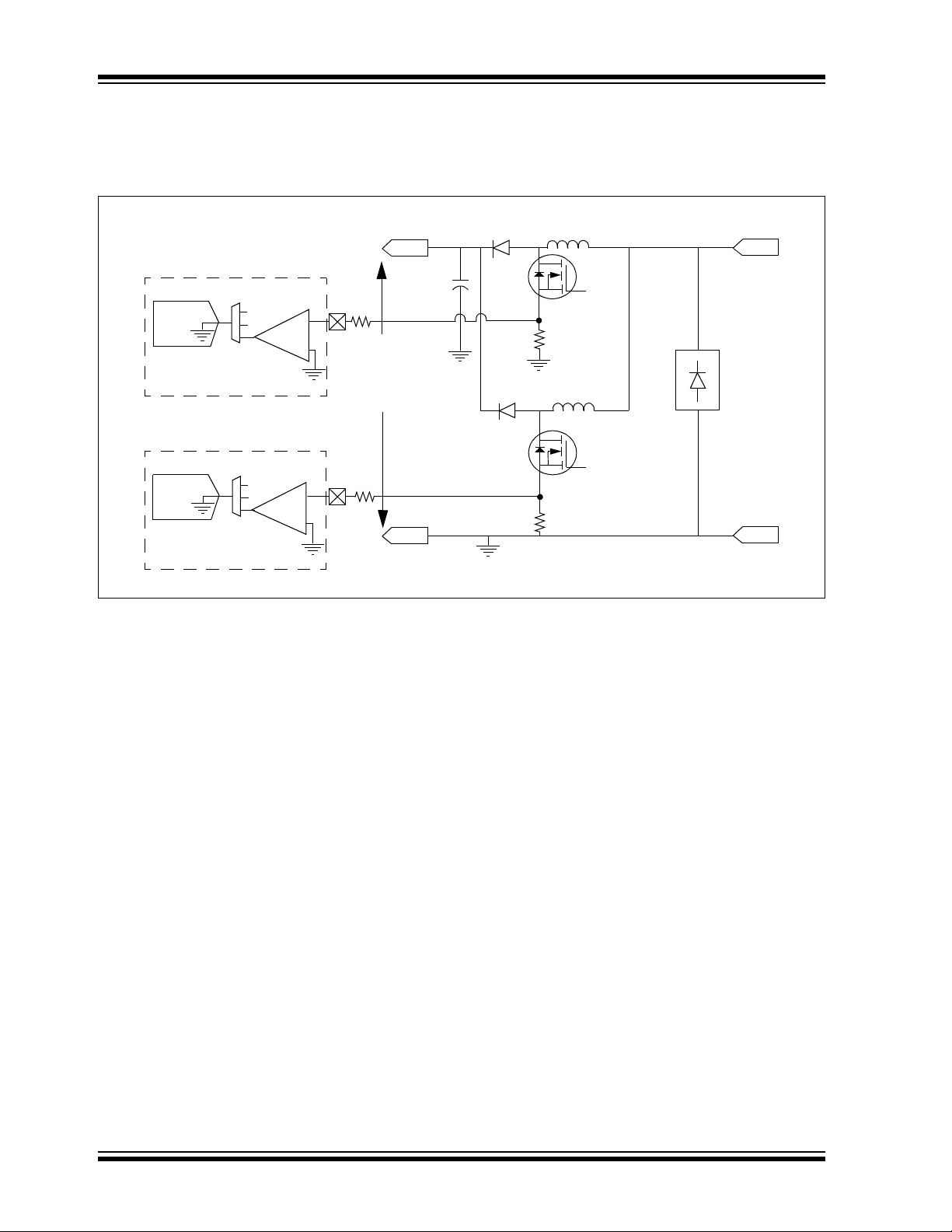
Figure 3-2 illustrates an example of an SMPS application using the PGA module. In this example,
the PGA amplifies the current through the shunt resistors, with the output of the PGA connected
directly to the ADC module and the PGA configured in Single-Ended mode.
Figure 3-2: PGA Application in Interleaved PFC
DS70005146B-page 8 2014-2015 Microchip Technology Inc.
Page 9

2014-2015 Microchip Technology Inc. DS70005146B-page 9
4.0 REGISTER MAPS
A summary of the registers associated with the PGA module is provided in Ta bl e 4 -1 .
Table 4-1: Programmable Gain Register Map
File Name Bit 15 Bit 14 Bit 13 Bit 12 Bit 11 Bit 10 Bit 9 Bit 8 Bit 7 Bit 6 Bit 5 Bit 4 Bit 3 Bit 2 Bit 1 Bit 0
PGAxCON PGAEN PGAOEN SELPI2 SELPI1 SELPI0 SELNI2 SELNI1 SELNI0
PGAxCAL
Legend: — = unimplemented, read as ‘0’. Reset values are shown in hexadecimal.
— — — — — — — — — — PGACAL<5:0> 0000
— — — — — GAIN2 GAIN1 GAIN0 0000
All
Resets
dsPIC33/PIC24 Family Reference Manual
Page 10

dsPIC33/PIC24 Family Reference Manual
5.0 RELATED APPLICATION NOTES
This section lists application notes that are related to this section of the manual. These
application notes may not be written specifically for the dsPIC33/PIC24 device families, but the
concepts are pertinent and could be used with modification and possible limitations. The current
application notes related to the PGA module are:
Title Application Note #
No related application notes are available at this time. N/A
Note: Please visit the Microchip web site (www.microchip.com) for additional application
notes and code examples for the dsPIC33/PIC24 families of devices.
DS70005146B-page 10 2014-2015 Microchip Technology Inc.
Page 11

Programmable Gain Amplifier (PGA)
6.0 REVISION HISTORY
Revision A (March 2014)
This is the initial released version of this document.
Revision B (March 2015)
Removes all references to differential operation throughout the document. These are replaced
with “operation with independent ground reference” or “independent ground reference”,
depending on context.
Resizes Figure 1-1 to place it with the introductory discussion on page 2; the diagram is
otherwise unchanged.
Other minor corrections throughout the document.
2014-2015 Microchip Technology Inc. DS70005146B-page 11
Page 12

dsPIC33/PIC24 Family Reference Manual
NOTES:
DS70005146B-page 12 2014-2015 Microchip Technology Inc.
Page 13

Note the following details of the code protection feature on Microchip devices:
YSTEM
CERTIFIED BY DNV
== ISO/TS 16949 ==
• Microchip products meet the specification contained in their particular Microchip Data Sheet.
• Microchip believes that its family of products is one of the most secure families of its kind on the market today, when used in the
intended manner and under normal conditions.
• There are dishonest and possibly illegal methods used to breach the code protection feature. All of these methods, to our
knowledge, require using the Microchip products in a manner outside the operating specifications contained in Microchip’s Data
Sheets. Most likely, the person doing so is engaged in theft of intellectual property.
• Microchip is willing to work with the customer who is concerned about the integrity of their code.
• Neither Microchip nor any other semiconductor manufacturer can guarantee the security of their code. Code protection does not
mean that we are guaranteeing the product as “unbreakable.”
Code protection is constantly evolving. We at Microchip are committed to continuously improving the code protection features of our
products. Attempts to break Microchip’s code protection feature may be a violation of the Digital Millennium Copyright Act. If such acts
allow unauthorized access to your software or other copyrighted work, you may have a right to sue for relief under that Act.
Information contained in this publication regarding device
applications and the like is provided only for your convenience
and may be superseded by updates. It is your responsibility to
ensure that your application meets with your specifications.
MICROCHIP MAKES NO REPRESENTATIONS OR
WARRANTIES OF ANY KIND WHETHER EXPRESS OR
IMPLIED, WRITTEN OR ORAL, STATUTORY OR
OTHERWISE, RELATED TO THE INFORMATION,
INCLUDING BUT NOT LIMITED TO ITS CONDITION,
QUALITY, PERFORMANCE, MERCHANTABILITY OR
FITNESS FOR PURPOSE. Microchip disclaims all liability
arising from this information and its use. Use of Microchip
devices in life support and/or safety applications is entirely at
the buyer’s risk, and the buyer agrees to defend, indemnify and
hold harmless Microchip from any and all damages, claims,
suits, or expenses resulting from such use. No licenses are
conveyed, implicitly or otherwise, under any Microchip
intellectual property rights.
Trademarks
The Microchip name and logo, the Microchip logo, dsPIC,
FlashFlex, flexPWR, JukeBlox, K
LANCheck, MediaLB, MOST, MOST logo, MPLAB,
OptoLyzer, PIC, PICSTART, PIC
SST, SST Logo, SuperFlash and UNI/O are registered
trademarks of Microchip Technology Incorporated in the
U.S.A. and other countries.
The Embedded Control Solutions Company and mTouch are
registered trademarks of Microchip Technology Incorporated
in the U.S.A.
Analog-for-the-Digital Age, BodyCom, chipKIT, chipKIT logo,
CodeGuard, dsPICDEM, dsPICDEM.net, ECAN, In-Circuit
Serial Programming, ICSP, Inter-Chip Connectivity, KleerNet,
KleerNet logo, MiWi, MPASM, MPF, MPLAB Certified logo,
MPLIB, MPLINK, MultiTRAK, NetDetach, Omniscient Code
Generation, PICDEM, PICDEM.net, PICkit, PICtail,
RightTouch logo, REAL ICE, SQI, Serial Quad I/O, Total
Endurance, TSHARC, USBCheck, VariSense, ViewSpan,
WiperLock, Wireless DNA, and ZENA are trademarks of
Microchip Technology Incorporated in the U.S.A. and other
countries.
SQTP is a service mark of Microchip Technology Incorporated
in the U.S.A.
Silicon Storage Technology is a registered trademark of
Microchip Technology Inc. in other countries.
GestIC is a registered trademarks of Microchip Technology
Germany II GmbH & Co. KG, a subsidiary of Microchip
Technology Inc., in other countries.
All other trademarks mentioned herein are property of their
respective companies.
© 2014-2015, Microchip Technology Incorporated, Printed in
the U.S.A., All Rights Reserved.
ISBN: 978-1-63277-152-0
EELOQ, KEELOQ logo, Kleer,
32
logo, RightTouch, SpyNIC,
QUALITY MANAGEMENT S
2014-2015 Microchip Technology Inc. DS70005146B-page 13
Microchip received ISO/TS-16949:2009 certification for its worldwide
headquarters, design and wafer fabrication facilities in Chandler and
Tempe, Arizona; Gresham, Oregon and design centers in California
and India. The Company’s quality system processes and procedures
are for its PIC
devices, Serial EEPROMs, microperipherals, nonvolatile memory and
analog products. In addition, Microchip’s quality system for the design
and manufacture of development systems is ISO 9001:2000 certified.
®
MCUs and dsPIC® DSCs, KEELOQ
®
code hopping
Page 14

Worldwide Sales and Service
AMERICAS
Corporate Office
2355 West Chandler Blvd.
Chandler, AZ 85224-6199
Tel: 480-792-7200
Fax: 480-792-7277
Technical Support:
http://www.microchip.com/
support
Web Address:
www.microchip.com
Atlanta
Duluth, GA
Tel: 678-957-9614
Fax: 678-957-1455
Austin, TX
Tel: 512-257-3370
Boston
Westborough, MA
Tel: 774-760-0087
Fax: 774-760-0088
Chicago
Itasca, IL
Tel: 630-285-0071
Fax: 630-285-0075
Cleveland
Independence, OH
Tel: 216-447-0464
Fax: 216-447-0643
Dallas
Addison, TX
Tel: 972-818-7423
Fax: 972-818-2924
Detroit
Novi, MI
Tel: 248-848-4000
Houston, TX
Tel: 281-894-5983
Indianapolis
Noblesville, IN
Tel: 317-773-8323
Fax: 317-773-5453
Los Angeles
Mission Viejo, CA
Tel: 949-462-9523
Fax: 949-462-9608
New York, NY
Tel: 631-435-6000
San Jose, CA
Tel: 408-735-9110
Canada - Toronto
Tel: 905-673-0699
Fax: 905-673-6509
ASIA/PACIFIC
Asia Pacific Office
Suites 3707-14, 37th Floor
Tower 6, The Gateway
Harbour City, Kowloon
Hong Kong
Tel: 852-2943-5100
Fax: 852-2401-3431
Australia - Sydney
Tel: 61-2-9868-6733
Fax: 61-2-9868-6755
China - Beijing
Tel: 86-10-8569-7000
Fax: 86-10-8528-2104
China - Chengdu
Tel: 86-28-8665-5511
Fax: 86-28-8665-7889
China - Chongqing
Tel: 86-23-8980-9588
Fax: 86-23-8980-9500
China - Dongguan
Tel: 86-769-8702-9880
China - Hangzhou
Tel: 86-571-8792-8115
Fax: 86-571-8792-8116
China - Hong Kong SAR
Tel: 852-2943-5100
Fax: 852-2401-3431
China - Nanjing
Tel: 86-25-8473-2460
Fax: 86-25-8473-2470
China - Qingdao
Tel: 86-532-8502-7355
Fax: 86-532-8502-7205
China - Shanghai
Tel: 86-21-5407-5533
Fax: 86-21-5407-5066
China - Shenyang
Tel: 86-24-2334-2829
Fax: 86-24-2334-2393
China - Shenzhen
Tel: 86-755-8864-2200
Fax: 86-755-8203-1760
China - Wuhan
Tel: 86-27-5980-5300
Fax: 86-27-5980-5118
China - Xian
Tel: 86-29-8833-7252
Fax: 86-29-8833-7256
ASIA/PACIFIC
China - Xiamen
Tel: 86-592-2388138
Fax: 86-592-2388130
China - Zhuhai
Tel: 86-756-3210040
Fax: 86-756-3210049
India - Bangalore
Tel: 91-80-3090-4444
Fax: 91-80-3090-4123
India - New Delhi
Tel: 91-11-4160-8631
Fax: 91-11-4160-8632
India - Pune
Tel: 91-20-3019-1500
Japan - Osaka
Tel: 81-6-6152-7160
Fax: 81-6-6152-9310
Japan - Tokyo
Tel: 81-3-6880- 3770
Fax: 81-3-6880-3771
Korea - Daegu
Tel: 82-53-744-4301
Fax: 82-53-744-4302
Korea - Seoul
Tel: 82-2-554-7200
Fax: 82-2-558-5932 or
82-2-558-5934
Malaysia - Kuala Lumpur
Tel: 60-3-6201-9857
Fax: 60-3-6201-9859
Malaysia - Penang
Tel: 60-4-227-8870
Fax: 60-4-227-4068
Philippines - Manila
Tel: 63-2-634-9065
Fax: 63-2-634-9069
Singapore
Tel: 65-6334-8870
Fax: 65-6334-8850
Taiwan - Hsin Chu
Tel: 886-3-5778-366
Fax: 886-3-5770-955
Taiwan - Kaohsiung
Tel: 886-7-213-7828
Taiwan - Taipei
Tel: 886-2-2508-8600
Fax: 886-2-2508-0102
Thailand - Bangkok
Tel: 66-2-694-1351
Fax: 66-2-694-1350
EUROPE
Austria - Wels
Tel: 43-7242-2244-39
Fax: 43-7242-2244-393
Denmark - Copenhagen
Tel: 45-4450-2828
Fax: 45-4485-2829
France - Paris
Tel: 33-1-69-53-63-20
Fax: 33-1-69-30-90-79
Germany - Dusseldorf
Tel: 49-2129-3766400
Germany - Munich
Tel: 49-89-627-144-0
Fax: 49-89-627-144-44
Germany - Pforzheim
Tel: 49-7231-424750
Italy - Milan
Tel: 39-0331-742611
Fax: 39-0331-466781
Italy - Venice
Tel: 39-049-7625286
Netherlands - Drunen
Tel: 31-416-690399
Fax: 31-416-690340
Poland - Warsaw
Tel: 48-22-3325737
Spain - Madrid
Tel: 34-91-708-08-90
Fax: 34-91-708-08-91
Sweden - Stockholm
Tel: 46-8-5090-4654
UK - Wokingham
Tel: 44-118-921-5800
Fax: 44-118-921-5820
01/27/15
DS70005146B-page 14 2014-2015 Microchip Technology Inc.
 Loading...