

Page 1

HIGHLIGHTS
Liquid Crystal Display (LCD)
This section of the manual contains the following major topics:
1.0 Introduction ....................................................................................................................... 2
2.0 LCD Registers................................................................................................................... 3
3.0 LCD Segment Pins Configuration..................................................................................... 6
4.0 LCD Clock Source Selection............................................................................................. 8
5.0 LCD Bias Types ................................................................................................................ 9
6.0 LCD Multiplex Types....................................................................................................... 21
7.0 Segment Enables............................................................................................................ 22
8.0 Pixel Control.................................................................................................................... 22
9.0 LCD Frame Frequency ................................................................................................... 22
10.0 LCD Waveform Generation............................................................................................. 22
11.0 LCD Interrupts................................................................................................................. 36
12.0 Configuring the LCD Module........................................................................................... 38
13.0 Operation During Sleep .................................................................................................. 39
14.0 Registers......................................................................................................................... 40
15.0 Revision History.............................................................................................................. 41
2010-2013 Microchip Technology Inc. DS30009740B-page 1
Page 2

dsPIC33/PIC24 Family Reference Manual
COM<7:0>
Timing Control
Data Bus
SOSC
FRC Oscillator
LPRC Oscillator
512
to
64
MUX
SEG<63:0>
To I/O Pins
32 x 16 (= 8x 64)
LCD DATA
LCDCON
LCDPS
LCDSEx
LCDDATA0
LCDDATA1
LCDDATA30
LCDDATA31
.
.
.
LCD Bias Generation
LCD Clock
Source Select
LCD
Charge Pump
64
8
Bias
Voltage
16
(Secondary Oscillator)
Resistor Ladder
1.0 INTRODUCTION
The Liquid Crystal Display (LCD) driver module generates the timing control to drive a Static or
Multiplexed LCD panel. In the 100-pin devices (PIC24FJXXXGA3XX), the module drives panels
of up to eight commons and up to 60 segments when 5 to 8 commons are used, and up to
64 segments when 1 to 4 commons are used. It also provides control of the LCD pixel data.
The LCD driver module supports:
• Direct driving of LCD panel
• Three LCD clock sources with selectable prescaler
• Up to eight commons:
- Static (one common)
- 1/2 Multiplex (two commons)
- 1/3 Multiplex (three commons)
- 1/8 Multiplex (eight commons)
• Up to 60 segments (in 100-pin devices when 1/5-1/8 Multiplex is selected), 64 (in 100-pin
devices when up to 1/4 Multiplex is selected), 46 (in 80-pin devices when 1/5-1/8 Multiplex
is selected), 50 (in 80-pin devices when up to 1/4 Multiplex is selected), 30 (in 64-pin
devices when 1/5-1/8 Multiplex is selected) and 34 (in 64-pin devices when up to
1/4 Multiplex is selected)
• Static, 1/2 or 1/3 LCD Bias
• On-chip Bias generator with dedicated charge pump to support a range of fixed and
variable Bias options
• Internal resistors for Bias voltage generation
• Software contrast control for LCD using the internal biasing
A simplified block diagram of the module is shown in Figure 1-1.
Figure 1-1: LCD Driver Module Block Diagram
DS30009740B-page 2 2010-2013 Microchip Technology Inc.
Page 3

2.0 LCD REGISTERS
The LCD driver module has 40 registers:
• LCD Control Register (LCDCON)
• LCD Phase Register (LCDPS)
• LCD Voltage Regulator Control Register (LCDREG)
• LCD Reference Ladder Control Register (LCDREF)
• Four LCD Segment Enable Registers (LCDSE3:LCDSE0)
• 32 LCD Data Registers (LCDDATA31:LCDDATA0)
The LCDCON register, shown in Register 2-1, controls the overall operation of the module. Once
the module is configured, the LCDEN (LCDCON<15>) bit is used to enable or disable the LCD
module. The LCD panel can also operate during Sleep by clearing the SLPEN (LCDCON<6>) bit.
The LCDPS register, shown in Register 2-2, configures the LCD clock source prescaler and the
type of waveform: Type-A or Type-B. For details on these features, see Section 4.0 “L CD Clock
Source Selection”, Table 14-1 and Section 10.0 “LCD Waveform Generation”.
Liquid Crystal Display (LCD)
2010-2013 Microchip Technology Inc. DS30009740B-page 3
Page 4

dsPIC33/PIC24 Family Reference Manual
LMUX<2:0> Multiplex Bias
111 1/8 MUX (COM<7:0>) 1/3
110 1/7 MUX (COM<6:0>) 1/3
101 1/6 MUX (COM<5:0>) 1/3
100 1/5 MUX (COM<4:0>) 1/3
011 1/4 MUX (COM<3:0>) 1/3
010 1/3 MUX (COM<2:0>) 1/2 or 1/3
001 1/2 MUX (COM<1:0>) 1/2 or 1/3
000 Static (COM0) Static
Register 2-1: LCDCON: LCD Control Register
R/W-0 U-0 R/W-0 U-0 U-0 U-0 U-0 U-0
LCDEN
bit 15 bit 8
U-0 R/W-0 R/C-0 R/W-0 R/W-0 R/W-0 R/W-0 R/W-0
— SLPEN WERR CS1 CS0 LMUX2 LMUX1 LMUX0
bit 7 bit 0
Legend: C = Clearable bit
R = Readable bit W = Writable bit U = Unimplemented bit, read as ‘0’
-n = Value at POR ‘1’ = Bit is set ‘0’ = Bit is cleared x = Bit is unknown
bit 15 LCDEN: LCD Driver Enable bit
bit 14 Unimplemented: Read as ‘0’
bit 13 LCDSIDL: LCD Stop in CPU Idle Mode Control bit
bit 12-7 Unimplemented: Read as ‘0’
bit 6 SLPEN: LCD Driver Enable in Sleep Mode bit
bit 5 WERR: LCD Write Failed Error bit
bit 4-3 CS<1:0>: Clock Source Select bits
bit 2-0 LMUX<2:0>: LCD Commons Select bits
— LCDSIDL — — — — —
1 = LCD driver module is enabled
0 = LCD driver module is disabled
1 = LCD driver halts in CPU Idle mode
0 = LCD driver continues to operate in CPU Idle mode
1 = LCD driver module is disabled in Sleep mode
0 = LCD driver module is enabled in Sleep mode
1 = LCDDATAx register is written while WA (LCDPS<4>) = 0 (must be cleared in software)
0 = No LCD write error
00 =FRC
01 =LPRC
1x =SOSC
DS30009740B-page 4 2010-2013 Microchip Technology Inc.
Page 5

Liquid Crystal Display (LCD)
Register 2-2: LCDPS: LCD Phase Register
U-0 U-0 U-0 U-0 U-0 U-0 U-0 U-0
— — — — — — — —
bit 15 bit 8
R/W-0 R/W-0 R-0 R-0 R/W-0 R/W-0 R/W-0 R/W-0
WFT BIASMD LCDA WA LP3 LP2 LP1 LP0
bit 7 bit 0
Legend: r = Reserved bit
R = Readable bit W = Writable bit U = Unimplemented bit, read as ‘0’
-n = Value at POR ‘1’ = Bit is set ‘0’ = Bit is cleared x = Bit is unknown
bit 15-8 Unimplemented: Read as ‘0’
bit 7 WFT: Waveform Type Select bit
1 = Type-B waveform (phase changes on each frame boundary)
0 = Type-A waveform (phase changes within each common type)
bit 6 BIASMD: Bias Mode Select bit
When LMUX<2:0> =
0 = Static Bias mode/1/3 Bias mode (do not set this bit to ‘1’)
When LMUX<2:0> = 001 or 010:
1 = 1/2 Bias mode
0 = 1/3 Bias mode
bit 5 LCDA: LCD Active Status bit
1 = LCD driver module is active
0 = LCD driver module is inactive
bit 4 WA: LCD Write Allow Status bit
1 = Write into the LCDDATAx registers is allowed
0 = Write into the LCDDATAx registers is not allowed
bit 3-0 LP<3:0>: LCD Prescaler Select bits
1111 = 1:16
1110 = 1:15
1101 = 1:14
1100 = 1:13
1011 = 1:12
1010 = 1:11
1001 = 1:10
1000 = 1:9
0111 = 1:8
0110 = 1:7
0101 = 1:6
0100 = 1:5
0011 = 1:4
0010 = 1:3
0001 = 1:2
0000 = 1:1
000 or 011-111:
2010-2013 Microchip Technology Inc. DS30009740B-page 5
Page 6

dsPIC33/PIC24 Family Reference Manual
3.0 LCD SEGMENT PINS CONFIGURATION
The LCDSEx registers configure the functions of the port pins. Setting the segment enable bit for
a particular segment configures that pin as an LCD driver. There are four LCD Segment Enable
registers, as shown in Table 3-1. The prototype LCDSEx register is shown in Register 3-1.
Table 3-1: LCDSEx Registers and Associated Segments
Register Segments
LCDSE0 Seg 15:Seg 0
LCDSE1 Seg 31:Seg 16
LCDSE2 Seg 47:Seg 32
LCDSE3 Seg 63:Seg 48
Once the module is initialized for the LCD panel, the individual bits of the LCDDATAx registers
are cleared, or set, to represent a clear or dark pixel, respectively.
Specific sets of LCDDATAx registers are used with specific segments and common signals. Each
bit represents a unique combination of a specific segment connected to a specific common.
Individual LCDDATAx bits are named by the convention, “SxxCy”, with “xx” as the segment
number and “y” as the common number. The relationship is summarized in Register 2-2. The
prototype LCDDATAx register is shown in Register 3-2.
Note: Not all LCDSEx and LCDDATAx registers are implemented in all devices. Refer to
the specific device data sheet for more details.
Register 3-1: LCDSEx: LCD Segment x Enable Register
R/W-0 R/W-0 R/W-0 R/W-0 R/W-0 R/W-0 R/W-0 R/W-0
SE(n+15) SE(n+14) SE(n+13) SE(n+12) SE(n+11) SE(n+10) SE(n+9) SE(n+8)
bit 15 bit 8
R/W-0 R/W-0 R/W-0 R/W-0 R/W-0 R/W-0 R/W-0 R/W-0
SE(n+7) SE(n+6) SE(n+5) SE(n+4) SE(n+3) SE(n+2) SE(n+1) SE(n)
bit 7 bit 0
Legend:
R = Readable bit W = Writable bit U = Unimplemented bit, read as ‘0’
-n = Value at POR ‘1’ = Bit is set ‘0’ = Bit is cleared x = Bit is unknown
bit 7-0 SE(n + 15):SE(n): Segment Enable bits
For LCDSE0: n = 0
For LCDSE1: n = 16
For LCDSE2: n = 32
For LCDSE3: n = 48
1 = Segment function of the pin is enabled; digital I/O is disabled
0 = Segment function of the pin is disabled
DS30009740B-page 6 2010-2013 Microchip Technology Inc.
Page 7

Liquid Crystal Display (LCD)
Register 3-2: LCDDATAx: LCD Data x Register
R/W-0 R/W-0 R/W-0 R/W-0 R/W-0 R/W-0 R/W-0 R/W-0
S(n+15)Cy S(n+14)Cy S(n+13)Cy S(n+12)Cy S(n+11)Cy S(n+10)Cy S(n+9)Cy S(n+8)Cy
bit 15 bit 8
R/W-0 R/W-0 R/W-0 R/W-0 R/W-0 R/W-0 R/W-0 R/W-0
S(n+7)Cy S(n+6)Cy S(n+5)Cy S(n+4)Cy S(n+3)Cy S(n+2)Cy S(n+1)Cy S(n)Cy
bit 7 bit 0
Legend:
R = Readable bit W = Writable bit U = Unimplemented bit, read as ‘0’
-n = Value at POR ‘1’ = Bit is set ‘0’ = Bit is cleared x = Bit is unknown
bit 15-0 S(n + 15)Cy:S(n)Cy: Pixel On bits
For registers, LCDDATA0 through LCDDATA3: n = (16x), y = 0
For registers, LCDDATA4 through LCDDATA7: n = (16(x – 4)), y = 1
For registers, LCDDATA8 through LCDDATA11: n = (16(x – 8)), y = 2
For registers, LCDDATA12 through LCDDATA15: n = (16(x – 12)), y = 3
For registers, LCDDATA16 through LCDDATA19: n = (16(x – 16)), y = 4
For registers, LCDDATA20 through LCDDATA23: n = (16(x – 20)), y = 5
For registers, LCDDATA24 through LCDDATA27: n = (16(x – 24)), y = 6
For registers, LCDDATA28 through LCDDATA31: n = (16(x – 28)), y = 7
1 = Pixel on
0 = Pixel off
Table 3-2: LCDDATAx Registers and Bits for Segment and COM Combinations
COM Lines
0
1
2
3
4
5
6
7
0 to 15 16 to 31 32 to 47 48 to 64
LCDDATA0
S00C0:S15C0
LCDDATA4
S00C1:S15C1
LCDDATA8
S00C2:S15C2
LCDDATA12
S00C3:S15C3
LCDDATA16
S00C4:S15C4
LCDDATA20
S00C5:S15C5
LCDDATA24
S00C6:S15C6
LCDDATA28
S00C7:S15C7
LCDDATA1
S16C0:S31C0
LCDDATA5
S16C1:S31C1
LCDDATA9
S16C2:S31C2
LCDDATA13
S16C3:S31C3
LCDDATA17
S16C4:S31C4
LCDDATA21
S16C5:S31C5
LCDDATA25
S16C6:S31C6
LCDDATA29
S16C7:S31C7
Segments
LCDDATA2
S32C0:S47C0
LCDDATA6
S32C1:S47C1
LCDDATA10
S32C2:S47C2
LCDDATA14
S32C3:S47C3
LCDDATA18
S32C4:S47C4
LCDDATA22
S32C5:S47C5
LCDDATA26
S32C6:S47C6
LCDDATA30
S32C7:S47C7
LCDDATA3
S48C0:S63C0
LCDDATA7
S48C1:S63C1
LCDDATA11
S48C2:S63C2
LCDDATA15
S48C3:S63C3
LCDDATA19
S48C4:S59C4
LCDDATA23
S48C5:S69C5
LCDDATA27
S48C6:S59C6
LCDDATA31
S48C7:S59C7
2010-2013 Microchip Technology Inc. DS30009740B-page 7
Page 8

dsPIC33/PIC24 Family Reference Manual
CS<1:0>
SOSC Oscillator
(32 kHz)
LPRC Oscillator
(31.25 kHz)
÷4
LMUX<2:0>
4-Bit Prog Prescaler
÷1, 2, 3....8
Ring Counter
LMUX<2:0>
COM0
COM1
COM2
COM7
÷8192
(8 MH
Z)
÷2
÷32
÷32
LP<2:0>
(LCDCON<4:3>)
(LCDCON<2:0>)
(LCDCON< 2:0>)
(LCDPS<2:0>)
FRC Oscillator
STAT
1/2 MUX
MUX
4.0 LCD CLOCK SOURCE SELECTION
The LCD driver module has three possible clock sources:
• FRC/8192
• SOSC Clock/32
•LPRC/32
The first clock source is the 8 MHz Fast Internal RC (FRC) oscillator, divided by 8,192. This
divider ratio is chosen to provide about 1 kHz output. The divider is not programmable. Instead,
the LCD Prescaler bits, LCDPS<3:0>, are used to set the LCD frame clock rate.
The second clock source is the SOSC oscillator/32. This also outputs about 1 kHz when a
32.768 kHz crystal is used with the SOSC oscillator. To use the SOSC oscillator as a clock
source, set the SOSCEN (OSCCON<1>) bit.
The third clock source is a 31.25 kHz internal LPRC oscillator/32 that provides approximately
1 kHz output.
The second and third clock sources may be used to continue running the LCD while the
processor is in Sleep.
These clock sources are selected through the bits, CS<1:0> (LCDCON<4:3>).
4.1 LCD Prescaler
A 16-bit counter is available as a prescaler for the LCD clock. The prescaler is not directly readable or writable. Its value is set by the LP<2:0> bits (LCDPS<2:0>) that determine the prescaler
assignment and prescale ratio.
Selectable prescale values are from 1:1 through 1:16, in increments of one.
Figure 4-1: LCD Clock Generation
DS30009740B-page 8 2010-2013 Microchip Technology Inc.
Page 9

5.0 LCD BIAS TYPES
The LCD module can be configured in one of three Bias types:
• Static Bias (Two Voltage Levels: V
• 1/2 Bias (Three Voltage Levels: VSS, 1/2 VDD and VDD)
• 1/3 Bias (Four Voltage Levels: VSS, 1/3 VDD, 2/3 VDD and VDD)
LCD Bias voltages can be generated with an internal resistor ladder, internal Bias generator or
external resistor ladder.
5.1 Internal Resistor Biasing
This mode does not use external resistors, but rather internal resistor ladders that are configured
to generate the Bias voltage.
The internal reference ladder actually consists of three separate ladders. Disabling the internal
reference ladder disconnects all of the ladders, allowing external voltages to be supplied.
Depending on the total resistance of the resistor ladders, the biasing can be classified as low,
medium or high power.
Table 5-1 shows the total resistance of each of the ladders. Figure 5-1 shows the internal resister
ladder connections. When the internal resistor ladder is selected, the Bias voltage will be internal;
it can also provide software contrast control (using LCDCST<2:0>).
Table 5-1: Internal Resistance Ladder Power Modes
Liquid Crystal Display (LCD)
SS and VDD)
Nominal
Power Mode
Low 3 MΩ 1 µA
Medium 300 kΩ 10 µA
High 30 kΩ 100 µA
Resistance of
Entire Ladder
DD
I
2010-2013 Microchip Technology Inc. DS30009740B-page 9
Page 10

dsPIC33/PIC24 Family Reference Manual
LCDBIAS3
LCDBIAS2
LCDBIAS1
VLCD3PE
VLCD2PE
VLCD1PE
LCDCST<2:0>
LCDIRE
LRLAT<2:0>
A Power Mode
B Power Mode
LRLAP<1:0> LRLBP<1:0>
Low
Resistor
Ladder
Medium
Resistor
Ladder
High
Resistor
Ladder
VDD
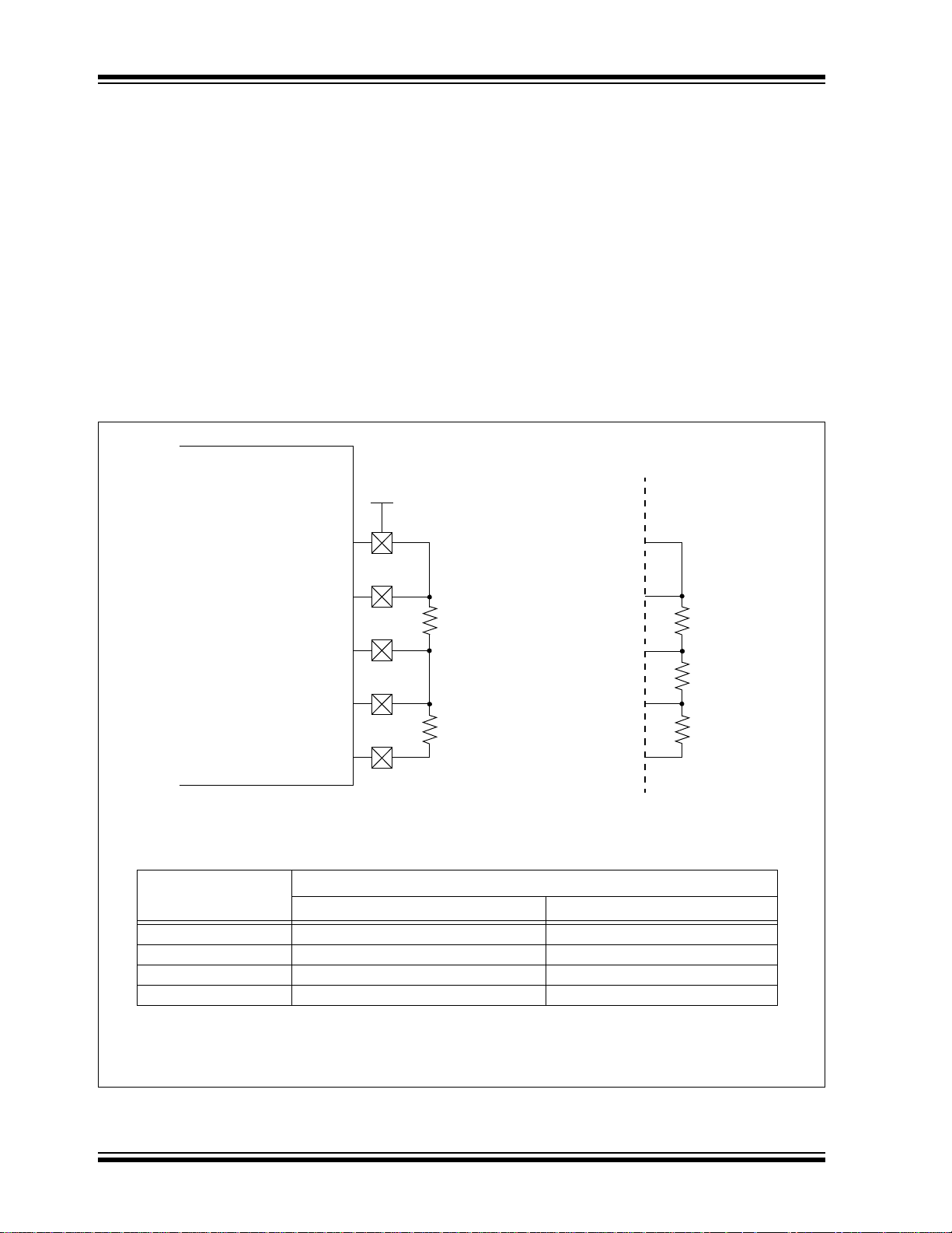
Figure 5-1: LCD Bias Internal Resistor Ladder Connection Diagram
There are two power modes, designated as “Mode A” and “Mode B”. Mode A is set by the bits,
LRLAP<1:0>, and Mode B by the LRLBP<1:0> bits. The resistor ladder to use for Modes A and
B are selected by the bits, LRLAP<1:0> and LRLBP<1:0>, respectively.
Each ladder has a matching contrast control ladder, tuned to the nominal resistance of the reference ladder. This contrast control resistor can be controlled by the LCDCST<2:0> bits
(LCDREF<13:11>). Disabling the internal reference ladder results in all of the ladders being
disconnected, allowing external voltages to be supplied.
To get additional current in High-Power mode, when LRLAP<1:0> (LCDREF<7:6>) = 11, both
the medium and high-power resistor ladders are activated.
Whenever the LCD module is inactive (LCDA (LCDPS<5>) = 0), the reference ladder will be
turned off.
DS30009740B-page 10 2010-2013 Microchip Technology Inc.
Page 11

Liquid Crystal Display (LCD)
Single Segment Time
‘H00 ‘H01 ‘H02 ‘H03 ‘H04 ‘H05 ‘H06 ‘H07 ‘H1E ‘H1F ‘H00 ‘H01
‘H3
Power Mode A Power Mode B Mode A
LRLAT<2:0>
lcd_32x_clk
cnt<4:0>
lcd_clk
LRLAT<2:0>
Segment Data
Power Mode
5.1.1 AUTOMATIC POWER MODE SWITCHING
As an LCD segment is electrically only a capacitor, current is drawn only during the interval when
the voltage is switching. To minimize total device current, the LCD reference ladder can be operated in a different power mode for the transition portion of the duration. This is controlled by the
LCDREF register.
Mode A Power mode is active for a programmable time, beginning at the time when the LCD
segment waveform is transitioning. The LRLAT<2:0> (LCDREF<2:0>) bits select how long the
transition or if the Mode A is active. Mode B Power mode is active for the remaining time before
the segments or commons change again.
As shown in Figure 5-2, there are 32 counts in a single segment time. Type-A can be chosen
during the time when the waveform is in transition. Type-B can be used when the clock is stable
or not in transition.
By using this feature of automatic power switching using Type-A/Type-B, the power consumption
can be optimized for a given contrast.
Figure 5-2: LCD Reference Ladder Power Mode Switching Diagram
2010-2013 Microchip Technology Inc. DS30009740B-page 11
Page 12

dsPIC33/PIC24 Family Reference Manual
LCDCST<2:0>
Analog
RR RR
7 Stages
MUX
To Top of
Reference Ladder
7
0
3
VDD
Internal Reference
Contrast Control
5.1.2 CONTRAST CONTROL
The LCD contrast control circuit consists of a 7-tap resistor ladder, controlled by the
LCDCST<2:0> bits (see Figure 5-3).
Figure 5-3: Internal Reference and Contrast Control Block Diagram
5.1.3 INTERNAL REFERENCE
Under firmware control, an internal reference for the LCD Bias voltages can be enabled. When
enabled, the source of this voltage can be V
When no internal reference is selected, the LCD contrast control circuit is disabled and the LCD
Bias must be provided externally. Whenever the LCD module is inactive (LCDA = 0), the internal
reference will be turned off.
DD.
5.1.4 VLCDxPE PINS
The VLCD3PE, VLCD2PE and VLCD1PE pins provide the ability for an external LCD Bias
network to be used instead of the internal ladder. Use of the VLCDxPE pins does not prevent use
of the internal ladder.
Each VLCDxPE pin has an independent control in the LCDREF register, allowing access to any
or all of the LCD Bias signals.
This architecture allows for maximum flexibility in different applications. The VLCDxPE pins could
be used to add capacitors to the internal reference ladder for increasing the drive capacity. For
applications where the internal contrast control is insufficient, the firmware can choose to enable
only the VLCD3PE pin, allowing an external contrast control circuit to use the internal reference
divider.
DS30009740B-page 12 2010-2013 Microchip Technology Inc.
Page 13

Liquid Crystal Display (LCD)
Register 5-1: LCDREF: LCD Reference Ladder Control Register
R/W-0 U-0 R/W-0 R/W-0 R/W-0 R/W-0 R/W-0 R/W-0
LCDIRE
bit 15 bit 8
R/W-0 R/W-0 R/W-0 R/W-0 U-0 R/W-0 R/W-0 R/W-0
LRLAP1 LRLAP0 LRLBP1 LRLBP0
bit 7 bit 0
Legend:
R = Readable bit W = Writable bit U = Unimplemented bit, read as ‘0’
-n = Value at POR ‘1’ = Bit is set ‘0’ = Bit is cleared x = Bit is unknown
bit 15 LCDIRE: LCD Internal Reference Enable bit
bit 14 Unimplemented: Read as ‘0’
bit 13-11 LCDCST<2:0>: LCD Contrast Control bits
bit 10 VLCD3PE: LCD Bias 3 Pin Enable bit
bit 9 VLCD2PE: LCD Bias 2 Pin Enable bit
bit 8 VLCD1PE: LCD Bias 1 Pin Enable bit
bit 7-6 LRLAP<1:0>: LCD Reference Ladder A Time Power Control bits
bit 5-4 LRLBP<1:0>: LCD Reference Ladder B Time Power Control bits
bit 3 Unimplemented: Read as ‘0’
— LCDCST2 LCDCST1 LCDCST0 VLCD3PE VLCD2PE VLCD1PE
— LRLAT2 LRLAT1 LRLAT0
1 = Internal LCD reference is enabled and connected to the internal contrast control circuit
0 = Internal LCD reference is disabled
Selects the Resistance of the LCD Contrast Control Resistor Ladder:
111 = Resistor ladder is at maximum resistance (minimum contrast)
110 = Resistor ladder is at 6/7th of maximum resistance
101 = Resistor ladder is at 5/7th of maximum resistance
100 = Resistor ladder is at 4/7th of maximum resistance
011 = Resistor ladder is at 3/7th of maximum resistance
010 = Resistor ladder is at 2/7th of maximum resistance
001 = Resistor ladder is at 1/7th of maximum resistance
000 = Minimum resistance (maximum contrast); resistor ladder is shorted
1 = Bias 3 level is connected to the external pin, LCDBIAS3
0 = Bias 3 level is internal (internal resistor ladder)
1 = Bias 2 level is connected to the external pin, LCDBIAS2
0 = Bias 2 level is internal (internal resistor ladder)
1 = Bias 1 level is connected to the external pin, LCDBIAS1
0 = Bias 1 level is internal (internal resistor ladder)
During Time Interval A:
11 = Internal LCD reference ladder is powered in High-Power mode
10 = Internal LCD reference ladder is powered in Medium Power mode
01 = Internal LCD reference ladder is powered in Low-Power mode
00 = Internal LCD reference ladder is powered down and unconnected
During Time Interval B:
11 = Internal LCD reference ladder is powered in High-Power mode
10 = Internal LCD reference ladder is powered in Medium Power mode
01 = Internal LCD reference ladder is powered in Low-Power mode
00 = Internal LCD reference ladder is powered down and unconnected
2010-2013 Microchip Technology Inc. DS30009740B-page 13
Page 14

dsPIC33/PIC24 Family Reference Manual
Register 5-1: LCDREF: LCD Reference Ladder Control Register (Continued)
bit 2-0 LRLAT<2:0>: LCD Reference Ladder A Time Interval Control bits
Sets the number of 32 clock counts when the A Time Interval Power mode is active.
For Type-A Waveforms (WFT =
111 = Internal LCD reference ladder is in A Power mode for 7 clocks and B Power mode for 9 clocks
110 = Internal LCD reference ladder is in A Power mode for 6 clocks and B Power mode for 10 clocks
101 = Internal LCD reference ladder is in A Power mode for 5 clocks and B Power mode for 11 clocks
100 = Internal LCD reference ladder is in A Power mode for 4 clocks and B Power mode for 12 clocks
011 = Internal LCD reference ladder is in A Power mode for 3 clocks and B Power mode for 13 clocks
010 = Internal LCD reference ladder is in A Power mode for 2 clocks and B Power mode for 14 clocks
001 = Internal LCD reference ladder is in A Power mode for 1 clock and B Power mode for 15 clocks
000 = Internal LCD reference ladder is always in B Power mode
For Type-B Waveforms (WFT =
111 = Internal LCD reference ladder is in A Power mode for 7 clocks and B Power mode for 25 clocks
110 = Internal LCD reference ladder is in A Power mode for 6 clocks and B Power mode for 26 clocks
101 = Internal LCD reference ladder is in A Power mode for 5 clocks and B Power mode for 27 clocks
100 = Internal LCD reference ladder is in A Power mode for 4 clocks and B Power mode for 28 clocks
011 = Internal LCD reference ladder is in A Power mode for 3 clocks and B Power mode for 29 clocks
010 = Internal LCD reference ladder is in A Power mode for 2 clocks and B Power mode for 30 clocks
001 = Internal LCD reference ladder is in A Power mode for 1 clock and B Power mode for 31 clocks
000 = Internal LCD reference ladder is always in B Power mode
0):
1):
5.2 LCD Bias Generation
The LCD driver module is capable of generating the required Bias voltages for LCD operation
with a minimum of external components. This includes the ability to generate the different voltage
levels required by the different Bias types that are required by the LCD. The driver module can
also provide Bias voltages, both above and below the microcontroller V
on-chip LCD voltage regulator.
5.2.1 LCD BIAS TYPES
There is support for three Bias types based on the waveforms generated to control segments and
commons:
• Static (two discrete levels)
• 1/2 Bias (three discrete levels
• 1/3 Bias (four discrete levels)
The use of different waveforms in driving the LCD is discussed in more detail in Section 10.0
“LCD Waveform Generation”.
5.2.2 LCD VOLTAGE REGULATOR
The purpose of the LCD regulator is to provide proper Bias voltage and good contrast for the
LCD, regardless of V
ence. The regulator can be configured by using external components to boost Bias voltage above
V
DD. It can also operate a display at a constant voltage below VDD. The regulator can also be
selectively disabled to allow Bias voltages to be generated by an external resistor network.
The LCD regulator is controlled through the LCDREG register (Register 5-2). It is enabled or disabled using the CKSEL<1:0> bits, while the charge pump can be selectively enabled using the
CPEN bit. When the regulator is enabled, the MODE13 bit is used to select the Bias type. The
peak LCD Bias voltage, measured as a difference between the potentials of LCDBIAS3 and
LCDBIAS0, is configured with the BIAS<2:0> bits.
DD levels. This module contains a charge pump and internal voltage refer-
DD, through the use of an
DS30009740B-page 14 2010-2013 Microchip Technology Inc.
Page 15

Liquid Crystal Display (LCD)
Register 5-2: LCDREG: LCD Voltage Regulator Control Register
R/W-0 U-0 U-0 U-0 U-0 U-0 U-0 U-0
CPEN
bit 15 bit 8
U-0 U-0 R/W-1 R/W-1 R/W-1 R/W-1 R/W-0 R/W-0
— — BIAS2 BIAS1 BIAS0 MODE13 CKSEL1 CKSEL 0
bit 7 bit 0
Legend:
R = Readable bit W = Writable bit U = Unimplemented bit, read as ‘0’
-n = Value at POR ‘1’ = Bit is set ‘0’ = Bit is cleared x = Bit is unknown
bit 15 CPEN: LCD Charge Pump Enable bit
bit 14-6 Unimplemented: Read as ‘0’
bit 5-3 BIAS<2:0>: Regulator Voltage Output Control bits
bit 2 MODE13: 1/3 LCD Bias Enable bit
bit 1-0 CKSEL<1:0>: Regulator Clock Source Select bits
— — — — — — —
1 = Charge pump enabled; highest LCD Bias voltage is 3.6V
0 = Charge pump disabled; highest LCD Bias voltage is AV
111 = 3.60V peak (offset on LCDBIAS0 of 0V)
110 = 3.47V peak (offset on LCDBIAS0 of 0.13V)
101 = 3.34V peak (offset on LCDBIAS0 of 0.26V)
100 = 3.21V peak (offset on LCDBIAS0 of 0.39V)
011 = 3.08V peak (offset on LCDBIAS0 of 0.52V)
010 = 2.95V peak (offset on LCDBIAS0 of 0.65V)
001 = 2.82V peak (offset on LCDBIAS0 of 0.78V)
000 = 2.69V peak (offset on LCDBIAS0 of 0.91V)
1 = Regulator output supports 1/3 LCD Bias mode
0 = Regulator output supports Static LCD Bias mode
11 = 31 kHz LPRC
10 =8 MHz FRC
01 =SOSC
00 = LCD regulator is disabled
DD
2010-2013 Microchip Technology Inc. DS30009740B-page 15
Page 16

dsPIC33/PIC24 Family Reference Manual
5.3 Bias Configurations
dsPIC33/PIC24 family devices have four distinct circuit configurations for LCD Bias generation:
• M0: Regulator with Boost
• M1: Regulator without Boost
• M2: Resistor Ladder with Software Contrast
• M3: Resistor Ladder with Hardware Contrast
5.3.1 M0 (REGULATOR WITH BOOST)
In M0 operation, the LCD charge pump feature is enabled. This allows the regulator to generate
voltages up to +3.6V to the LCD (as measured at LCDBIAS3).
M0 uses a Flyback Capacitor connected between V
on LCDBIAS0 through LCDBIAS3, to obtain the required voltage boost (Figure 5-4). The output
voltage (VBIAS) is the difference of the potential between LCDBIAS3 and LCDBIAS0. It is set by
the BIAS<2:0> bits, which adjust the offset between LCDBIAS0 and V
FLY) acts as a charge storage element for large LCD loads. This mode is useful in those cases
(C
where the voltage requirements of the LCD are higher than the microcontroller’s V
mits software control of the display’s contrast, by adjustment of the Bias voltage, by changing the
value of the BIASx bits.
M0 supports Static and 1/3 Bias types. Generation of the voltage levels for 1/3 Bias is handled
automatically, but must be configured in software.
M0 is enabled by selecting a valid regulator clock source (CKSEL<1:0> set to any value except
‘00’) and setting the CPEN bit. If a Static Bias type is required, the MODE13 bit must be cleared.
LCAP1 and VLCAP2, as well as filter capacitors
SS. The Flyback Capacitor
DD. It also per-
5.3.2 M1 (REGULATOR WITHOUT BOOST)
M1 operation is similar to M0, but does not use the LCD charge pump. It can provide VBIAS up
to the voltage level supplied directly to LCDBIAS3. It can be used in cases where V
application is expected to never drop below a level that can provide adequate contrast for the
LCD. The connection of external components is very similar to M0, except that LCDBIAS3 must
be tied directly to V
DD (Figure 5-4).
Note: When the device is put to Sleep while operating in M0 or M1 mode, make sure that
the Bias capacitors are fully discharged to get the lowest Sleep current.
• The BIAS<2:0> bits can still be used to adjust contrast in software by changing VBIAS. As
with M0, changing these bits changes the offset between LCDBIAS0 and V
SS. In M1, this is
reflected in the change between the LCDBIAS0 and the voltage tied to LCDBIAS3. Thus, if
DD should change, VBIAS will also change; where in M0, the level of VBIAS is constant.
V
• Like M0, M1 supports Static and 1/3 Bias types. Generation of the voltage levels for
1/3 Bias is handled automatically, but must be configured in software. M1 is enabled by
selecting a valid regulator clock source (CKSEL<1:0> set to any value except ‘00’) and
clearing the CPEN bit. If 1/3 Bias type is required, the MODE13 bit should also be set.
DD for the
DS30009740B-page 16 2010-2013 Microchip Technology Inc.
Page 17

Liquid Crystal Display (LCD)
LCDBIAS3
LCDBIAS2
LCDBIAS1
LCDBIAS0
AV
DD
VDD
VLCAP1
VLCAP2
CFLY
C0
C1
C2
C3
C0
C1
C2
VDD
VDD
Mode 0 (VBIAS up to 3.6V) Mode 1 (VBIAS VDD)
CFLY
Note 1: These values are provided for design guidance only. They should be optimized for the application by the designer
based on the actual LCD specifications.
0.47 F
(1)
0.47 F
(1)
0.47 F
(1)
0.47 F
(1)
0.47 F
(1)
0.47 F
(1)
0.47 F
(1)
0.47 F
(1)
0.47 F
(1)
dsPIC33/PIC24
Figure 5-4: LCD Regulator Connections for M0 and M1 Configurations
2010-2013 Microchip Technology Inc. DS30009740B-page 17
Page 18
dsPIC33/PIC24 Family Reference Manual
LCDBIAS3
Note 1: These values are provided for design guidance only. They should be optimized for the application by the
designer based on the actual LCD specifications.
Bias Level at Pin
Bias Type
1/2 Bias 1/3 Bias
LCDBIAS0 (Internal Low Reference Voltage) (Internal Low Reference Voltage)
LCDBIAS1 1/2 V
BIAS 1/3 VBIAS
LCDBIAS2 1/2 VBIAS 2/3 VBIAS
LCDBIAS3 VBIAS (up to AVDD)VBIAS (up to AVDD)
10 k
(1)
10 k
(1)
1/2 Bias 1/3 Bias
LCDBIAS2
LCDBIAS1
LCDBIAS0
AV
DD
10 k
(1)
10 k
(1)
10 k
(1)
VDD
dsPIC33/PIC24
5.3.3 M2 (RESISTOR LADDER WITH SOFTWARE CONTRAST)
M2 operation also uses the LCD regulator but disables the charge pump. The regulator’s internal
voltage reference remains active as a way to regulate contrast. It is used in cases where the
current requirements of the LCD exceed the capacity of the regulator’s charge pump.
In this configuration, the LCD Bias voltage levels are created by an external resistor voltage
divider, connected across LCDBIAS0 through LCDBIAS3, with the top of the divider tied to V
(Figure 5-5). The potential at the bottom of the ladder is determined by the LCD regulator’s voltage reference, tied internally to LCDBIAS0. The Bias type is determined by the voltages on the
LCDBIAS pins, which are controlled by the configuration of the resistor ladder. Most applications
using M2 will use a 1/3 or 1/2 Bias type. While Static Bias can also be used, it offers extremely
limited contrast range and additional current consumption over other Bias Generation modes.
Like M1, the LCDBIAS bits can be used to control contrast, limited by the level of V
to the device. Also, since there is no capacitor required across V
are available as digital I/O ports: RG2 and RG3. M2 is selected by clearing the CKSEL<1:0> bits
and setting the CPEN bit.
Figure 5-5: Resistor Ladder Connections for M2 Configuration
LCAP1 and VLCAP2, these pins
DD
DD supplied
DS30009740B-page 18 2010-2013 Microchip Technology Inc.
Page 19

Liquid Crystal Display (LCD)
LCDBIAS3
Note 1: These values are provided for design guidance only. They should be optimized for the application by the
designer based on the actual LCD specifications.
2: A potentiometer for manual contrast adjustment is optional; it may be omitted entirely.
Bias Level at Pin
Bias Type
Static 1/2 Bias 1/3 Bias
LCDBIAS0 AV
SS AVSS AVSS
LCDBIAS1 AVSS 1/2 AVDD 1/3 AVDD
LCDBIAS2 AVDD 1/2 AVDD 2/3 AVDD
LCDBIAS3 AVDD AVDD AVDD
10 k
(1)
10 k
(1)
Static Bias 1/2 Bias 1/3 Bias
LCDBIAS2
LCDBIAS1
LCDBIAS0
AV
DD
10 k
(1)
10 k
(1)
10 k
(1)
VDD
(2)
dsPIC33/PIC24
5.3.4 M3 (RESISTOR LADDER WITH HARDWARE CONTRAST)
In M3, the LCD regulator is completely disabled. Like M2, LCD Bias levels are tied to AVDD and
are generated using an external divider. The difference is that the internal voltage reference is
also disabled and the bottom of the ladder is tied to ground (V
the resistors, and the difference between V
ware adjustment is possible. This configuration is also used where the LCD module’s current
requirements exceed the capacity of the charge pump and software contrast control is not
needed.
Depending on the Bias type required, resistors are connected between some or all of the pins. A
potentiometer can also be connected between LCDBIAS3 and V
controlled contrast adjustment.
M3 is selected by clearing the CKSEL<1:0> and CPEN bits.
Figure 5-6: Resistor Ladder Connections for M3 Configuration
SS and VDD, determine the contrast range; no soft-
SS) (see Figure 5-6). The value of
DD to allow for hardware
2010-2013 Microchip Technology Inc. DS30009740B-page 19
Page 20

dsPIC33/PIC24 Family Reference Manual
I = C x
dV
dT
5.4 Design Considerations for the LCD Charge Pump
When designing applications that use the LCD regulator with the charge pump enabled, users
must always consider both the dynamic current and RMS (Static) current requirements of the display, and what the charge pump can deliver. Both dynamic and Static current can be determined
by Equation 5-1:
Equation 5-1:
For dynamic current, C is the value of the capacitors attached to LCDBIAS3 and LCDBIAS2. The
variable, dV, is the voltage drop allowed on C2 and C3 during a voltage switch on the LCD
display, and dT is the duration of the transient current after a clock pulse occurs.
For practical design purposes, these will be assumed to be 0.047 ìF for C, 0.1V for dV and 1 ìs
for dT. This yields a dynamic current of 4.7 mA for 1 ìs.
RMS (Root Mean Square) current is determined by the value of C
LCAP1 and VLCAP2 for dV, and the regulator clock period (TPER) for dT. Assuming a CFLY value
V
of 0.047 ìF, a value of 1.02V across C
rent will be 1.8 mA. Since the charge pump must charge five capacitors, the maximum current
becomes 360 ìA.
For a real world assumption of 50% efficiency, this yields a practical current of 180 ìA. Users
should compare the calculated current capacity against the requirements of the LCD. While dV
and dT are relatively fixed by device design, the values of C
LCDBIAS pins can be changed to increase or decrease current. As always, any changes should
be evaluated in the actual circuit for their impact on the application.
FLY and a TPER of 30, the maximum theoretical Static cur-
FLY for C, the voltage across
FLY and the capacitors on the
DS30009740B-page 20 2010-2013 Microchip Technology Inc.
Page 21

Liquid Crystal Display (LCD)
6.0 LCD MULTIPLEX TYPES
The LCD driver module can be configured into four Multiplex types:
• Static (only COM0 used)
• 1/2 Multiplex (COM0 and COM1 are used)
• 1/3 Multiplex (COM0, COM1 and COM2 are used)
• 1/4 Multiplex (COM0, COM1, COM2 and COM3 are used)
• 1/5 Multiplex (COM0, COM1, COM2, COM3 and COM4 are used)
• 1/6 Multiplex (COM0, COM1, COM2, COM3, COM4 and COM5 are used)
• 1/7 Multiplex (COM0, COM1, COM2, COM3, COM4, COM5 and COM6 are used)
• 1/8 Multiplex (COM0, COM1, COM2, COM3, COM4, COM5, COM6 and COM7 are used)
The LMUX<2:0> bits setting (LCDCON<2:0>) decides the function of the COM pins. (For details,
see Tabl e 6 -1 .)
If the pin is a digital I/O, the corresponding TRIS bit controls the data direction. If the pin is a COM
drive, the TRIS setting of that pin is overridden.
Note: On a Power-on Reset, the LMUX<2:0> bits are ‘000’.
Table 6-1: COM<7:0> Pin Function
LMUX<2:0> COM7 Pin COM6 Pin COM5 Pin CO M4 Pin COM3 Pin COM2 Pin COM1 Pin COM0 Pin
111 COM7 COM6 COM5 COM4 COM3 COM2 COM1 COM0
110 I/O Pin COM6 COM5 COM4 COM3 COM2 COM1 COM0
101 I/O Pin I/O Pin COM5 COM4 COM3 COM2 COM1 COM0
100 I/O Pin I/O Pin I/O Pin COM4 COM3 COM2 COM1 COM0
011 I/O Pin I/O Pin I/O Pin I/O Pin COM3 COM2 COM1 COM0
010 I/O Pin I/O Pin I/O Pin I/O Pin I/O Pin COM2 COM1 COM0
001 I/O Pin I/O Pin I/O Pin I/O Pin I/O Pin I/O Pin COM1 COM0
000 I/O Pin I/O Pin I/O Pin I/O Pin I/O Pin I/O Pin I/O Pin COM0
Note: Pins, COM<7:4>, can also be used as SEG pins when 1/4 Multiplex to Static Multiplex are used. These
pins can be used as I/O pins only if the respective bits in the LCDSEx registers are set to ‘0’.
2010-2013 Microchip Technology Inc. DS30009740B-page 21
Page 22

dsPIC33/PIC24 Family Reference Manual
7.0 SEGMENT ENABLES
The LCDSEx registers are used to select the pin function for each segment pin. The selection
allows each pin to operate as either an LCD segment driver or a digital only pin. To configure the
pin as a segment driver, the corresponding bits in the LCDSEx registers must be set to ‘1’.
If the pin is a digital I/O, the corresponding TRIS bit controls the data direction. Any bit set in the
LCDSEx registers overrides any bit settings in the corresponding TRIS register.
Note: On a Power-on Reset, these pins are configured as digital I/O.
8.0 PIXEL CO NT R OL
The LCDDATAx registers contain bits that define the state of each pixel. Each bit defines one
unique pixel. Tab le 3 -2 shows the correlation of each bit in the LCDDATAx registers to the
respective common and segment signals.
Any LCD pixel location not being used for display can be used as general purpose RAM.
9.0 LCD FRAME FREQUENCY
The rate at which the COM and SEG outputs change is called the LCD frame frequency.
Table 9-1: Frame Frequency Formulas
Multiplex Frame Frequency =
Static (000) Clock Source/(4 x 1 x (LP<3:0> + 1))
1/2 (001) Clock Source/(2 x 2 x (LP<3:0> + 1))
1/3 (010) Clock Source/(1 x 3 x (LP<3:0> + 1))
1/4 (011) Clock Source/(1 x 4 x (LP<3:0> + 1))
1/5 (100) Clock Source/(1 x 5 x (LP<3:0> + 1))
1/6 (101) Clock Source/(1 x 6 x (LP<3:0> + 1))
1/7 (110) Clock Source/(1 x 7 x (LP<3:0> + 1))
1/8 (111) Clock Source/(1 x 8 x (LP<3:0> + 1))
Note: The clock source is FRC/8192, SOSC/32 or LPRC/32.
10.0 LCD WAVEFORM GENERATION
LCD waveform generation is based on the philosophy that the net AC voltage across the dark
pixel should be maximized and the net AC voltage across the clear pixel should be minimized.
The net DC voltage across any pixel should be zero.
The COM signal represents the time slice for each common, while the SEG contains the pixel data.
The pixel signal (COM-SEG) will have no DC component and can take only one of the two RMS
values. The higher RMS value will create a dark pixel and a lower RMS value will create a clear
pixel.
As the number of commons increases, the delta between the two RMS values decreases. The
delta represents the maximum contrast that the display can have.
The LCDs can be driven by two types of waveforms: Type-A and Type-B. In a Type-A waveform,
the phase changes within each common type, whereas a Type-B waveform’s phase changes on
each frame boundary. Thus, Type-A waveforms maintain 0 V
Type-B waveforms take two frames.
DC over a single frame, whereas
Note: If Sleep has to be executed with LCD Sleep enabled (SLPEN (LCDCON<6>) = 1),
care must be taken to execute Sleep only when the V
DS30009740B-page 22 2010-2013 Microchip Technology Inc.
DC on all the pixels is ‘0’.
Page 23

Liquid Crystal Display (LCD)
V
1
V
0
COM0
SEG0
COM0-SEG0
COM0-SEG1
SEG1
V
1
V
0
V
1
V
0
V
0
V
1
-V
1
V
0
1 Frame
COM0
SEG0
SEG1
SEG2
SEG3
SEG4
SEG5
SEG6
SEG7
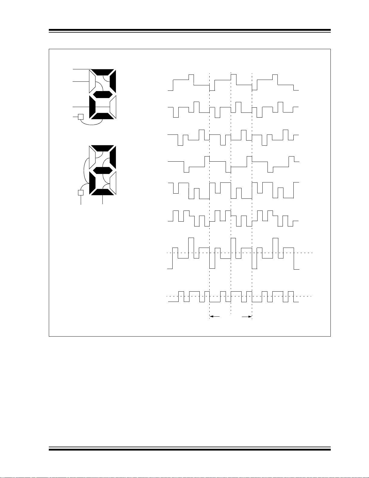
Figure 10-1 through Figure 10-13 provide waveforms for Static, Half-Multiplex, One-Third
Multiplex and Quarter Multiplex drives for Type-A and Type-B waveforms.
Figure 10-1: Type-A/Type-B Waveforms in Static Drive
2010-2013 Microchip Technology Inc. DS30009740B-page 23
Page 24

V
2
V
1
V
0
V
2
V
1
V
0
V
2
V
1
V
0
V
2
V
1
V
0
V
2
V
1
V
0
-V
2
-V
1
V
2
V
1
V
0
-V
2
-V
1
COM0
COM1
SEG0
SEG1
COM0-SEG0
COM0-SEG1
1 Frame
COM1
COM0
SEG0
SEG1
SEG2
SEG3
dsPIC33/PIC24 Family Reference Manual
Figure 10-2: Type-A Waveforms in 1/2 MUX, 1/2 Bias Drive
DS30009740B-page 24 2010-2013 Microchip Technology Inc.
Page 25

V
2
V
1
V
0
V
2
V
1
V
0
V
2
V
1
V
0
V
2
V
1
V
0
V
2
V
1
V
0
-V
2
-V
1
V
2
V
1
V
0
-V
2
-V
1
COM0
COM1
SEG0
SEG1
COM0-SEG0
COM0-SEG1
COM1
COM0
SEG0
SEG1
SEG2
SEG3
2 Frames
Liquid Crystal Display (LCD)
Figure 10-3: Type-B Waveforms in 1/2 MUX, 1/2 Bias Drive
2010-2013 Microchip Technology Inc. DS30009740B-page 25
Page 26

V
3
V
2
V
1
V
0
V
3
V
2
V
1
V
0
V
3
V
2
V
1
V
0
V
3
V
2
V
1
V
0
V
3
V
2
V
1
V
0
-V
3
-V
2
-V
1
V
3
V
2
V
1
V
0
-V
3
-V
2
-V
1
COM0
COM1
SEG0
SEG1
COM0-SEG0
COM0-SEG1
1 Frame
COM1
COM0
SEG0
SEG1
SEG2
SEG3
dsPIC33/PIC24 Family Reference Manual
Figure 10-4: Type-A Waveforms in 1/2 MUX, 1/3 Bias Drive
DS30009740B-page 26 2010-2013 Microchip Technology Inc.
Page 27

V
3
V
2
V
1
V
0
V
3
V
2
V
1
V
0
V
3
V
2
V
1
V
0
V
3
V
2
V
1
V
0
V
3
V
2
V
1
V
0
-V
3
-V
2
-V
1
V
3
V
2
V
1
V
0
-V
3
-V
2
-V
1
COM0
COM1
SEG0
SEG1
COM0-SEG0
COM0-SEG1
COM1
COM0
SEG0
SEG1
SEG2
SEG3
2 Frames
Liquid Crystal Display (LCD)
Figure 10-5: Type-B Waveforms in 1/2 MUX, 1/3 Bias Drive
2010-2013 Microchip Technology Inc. DS30009740B-page 27
Page 28

dsPIC33/PIC24 Family Reference Manual
V
2
V
1
V
0
V
2
V
1
V
0
V
2
V
1
V
0
V
2
V
1
V
0
V
2
V
1
V
0
V
2
V
1
V
0
-V
2
-V
1
V
2
V
1
V
0
-V
2
-V
1
COM0
COM1
COM2
SEG0
SEG1
COM0-SEG0
COM0-SEG1
COM2
COM1
COM0
SEG0
SEG1
SEG2
SEG2
1 Frame
Figure 10-6: Type-A Waveforms in 1/3 MUX, 1/2 Bias Drive
DS30009740B-page 28 2010-2013 Microchip Technology Inc.
Page 29

V
2
V
1
V
0
V
2
V
1
V
0
V
2
V
1
V
0
V
2
V
1
V
0
V
2
V
1
V
0
V
2
V
1
V
0
-V
2
-V
1
V
2
V
1
V
0
-V
2
-V
1
COM0
COM1
COM2
SEG0
SEG1
COM0-SEG0
COM0-SEG1
COM2
COM1
COM0
SEG0
SEG1
SEG2
2 Frames
Liquid Crystal Display (LCD)
Figure 10-7: Type-B Waveforms in 1/3 MUX, 1/2 Bias Drive
2010-2013 Microchip Technology Inc. DS30009740B-page 29
Page 30

V
3
V
2
V
1
V
0
V
3
V
2
V
1
V
0
V
3
V
2
V
1
V
0
V
3
V
2
V
1
V
0
V
3
V
2
V
1
V
0
V
3
V
2
V
1
V
0
-V
3
-V
2
-V
1
V
3
V
2
V
1
V
0
-V
3
-V
2
-V
1
COM0
COM1
COM2
SEG0
SEG1
COM0-SEG0
COM0-SEG1
COM2
COM1
COM0
SEG0
SEG1
SEG2
SEG2
1 Frame
dsPIC33/PIC24 Family Reference Manual
Figure 10-8: Type-A Waveforms in 1/3 MUX, 1/3 Bias Drive
DS30009740B-page 30 2010-2013 Microchip Technology Inc.
Page 31

V
3
V
2
V
1
V
0
V
3
V
2
V
1
V
0
V
3
V
2
V
1
V
0
V
3
V
2
V
1
V
0
V
3
V
2
V
1
V
0
V
3
V
2
V
1
V
0
-V
3
-V
2
-V
1
V
3
V
2
V
1
V
0
-V
3
-V
2
-V
1
COM0
COM1
COM2
SEG0
SEG1
COM0-SEG0
COM0-SEG1
COM2
COM1
COM0
SEG0
SEG1
SEG2
2 Frames
Liquid Crystal Display (LCD)
Figure 10-9: Type-B Waveforms in 1/3 MUX, 1/3 Bias Drive
2010-2013 Microchip Technology Inc. DS30009740B-page 31
Page 32

dsPIC33/PIC24 Family Reference Manual
V
3
V
2
V
1
V
0
V
3
V
2
V
1
V
0
V
3
V
2
V
1
V
0
V
3
V
2
V
1
V
0
V
3
V
2
V
1
V
0
V
3
V
2
V
1
V
0
V
3
V
2
V
1
V
0
-V
3
-V
2
-V
1
V
3
V
2
V
1
V
0
-V
3
-V
2
-V
1
COM0
COM1
COM2
COM3
SEG0
SEG1
COM0-SEG0
COM0-SEG1
COM3
COM2
COM1
COM0
1 Frame
SEG0
SEG1
Figure 10-10: Type-A Waveforms in 1/4 MUX, 1/3 Bias Drive
DS30009740B-page 32 2010-2013 Microchip Technology Inc.
Page 33
Liquid Crystal Display (LCD)
V
3
V
2
V
1
V
0
V
3
V
2
V
1
V
0
V
3
V
2
V
1
V
0
V
3
V
2
V
1
V
0
V
3
V
2
V
1
V
0
V
3
V
2
V
1
V
0
V
3
V
2
V
1
V
0
-V
3
-V
2
-V
1
V
3
V
2
V
1
V
0
-V
3
-V
2
-V
1
COM0
COM1
COM2
COM3
SEG0
SEG1
COM0-SEG0
COM0-SEG1
COM3
COM2
COM1
COM0
2 Frames
SEG0
SEG1
Figure 10-11: Type-B Waveforms in 1/4 MUX, 1/3 Bias Drive
2010-2013 Microchip Technology Inc. DS30009740B-page 33
Page 34

dsPIC33/PIC24 Family Reference Manual
COM4
COM3
COM2
COM1
SEG0
COM5
COM7
COM6
COM0
COM0
COM1
COM2
COM7
SEG0
COM0-SEG0
COM1-SEG0
V
3
V
2
V
1
V
0
V
3
V
2
V
1
V
0
V
3
V
2
V
1
V
0
V
3
V
2
V
1
V
0
V
3
V
2
V
1
V
0
-V
3
-V
2
-V
1
V
3
V
2
V
1
V
0
-V
3
-V
2
-V
1
V
3
V
2
V
1
V
0
Figure 10-12: Type-A Waveforms in 1/8 MUX, 1/3 Bias Drive
DS30009740B-page 34 2010-2013 Microchip Technology Inc.
Page 35

Liquid Crystal Display (LCD)
COM4
COM3
COM2
COM1
SEG0
COM5
COM7
COM6
COM0
V3
V2
COM0
V1
V0
V3
V2
V1
COM1
V0
V3
V2
V1
COM2
V0
V3
V2
V1
COM7
V0
V3
V2
SEG0
V1
V0
V3
V2
V1
V0
COM0 - SEG0
-V1
-V2
-V3
V3
V2
V1
V0
COM1 - SEG0
-V1
-V2
-V3
Figure 10-13: Type-B Waveforms in 1/8 MUX, 1/3 Bias Drive
2010-2013 Microchip Technology Inc. DS30009740B-page 35
Page 36

dsPIC33/PIC24 Family Reference Manual
11.0 LCD INTERRUPTS
The LCD timing generation provides an interrupt that defines the LCD frame timing. This interrupt
can be used to coordinate the writing of the pixel data with the start of a new frame, which
produces a visually crisp transition of the image.
This interrupt can also be used to synchronize external events to the LCD. For example, the interface to an external segment driver can be synchronized for segment data updates to the LCD
frame.
A new frame is defined as beginning at the leading edge of the COM0 common signal. The
interrupt will be set immediately after the LCD controller completes accessing all pixel data
required for a frame. This will occur at a fixed interval before the frame boundary (T
shown in Figure 11-1.
The LCD controller will begin to access data for the next frame, within the interval from the interrupt to when the controller begins accessing data after the interrupt (T
written within T
frame.
When the LCD driver is running with Type-B waveforms and the LMUX<2:0> bits are not equal
to ‘00’, there are some additional issues.
Since the DC voltage on the pixel takes two frames to maintain 0V, the pixel data must not
change between subsequent frames. If the pixel data was allowed to change, the waveform for
the odd frames would not necessarily be the complement of the waveform generated in the even
frames, and a DC component would be introduced into the panel. Because of this, using Type-B
waveforms requires synchronizing the LCD pixel updates to occur within a subframe after the
frame interrupt.
To correctly sequence writing in Type-B, the interrupt only occurs on complete phase intervals. If
the user attempts to write when the write is disabled, the WERR bit (LCDCON<5>) is set.
FWR, as this is when the LCD controller will begin to access the data for the next
FWR). New data must be
FINT), as
Note: The interrupt is not generated when the Type-A waveform is selected and when the
Type-B with no Multiplex (Static) is selected.
DS30009740B-page 36 2010-2013 Microchip Technology Inc.
Page 37

Liquid Crystal Display (LCD)
Frame
Boundary
Frame
Boundary
LCD
Interrupt
Occurs
Controller Accesses
Next Frame Data
TFINT
TFWR
TFWR =TFRAME/2 * (LMUX<2:0> + 1) + TCY/2
T
FINT =(TFWR/2 – (2 TCY + 40 ns)) Minimum = 1.5(TFRAME/4) – (2 TCY + 40 ns)
(T
FWR/2 – (1 TCY + 40 ns)) Maximum = 1.5(TFRAME/4) – (1 TCY + 40 ns)
Frame
Boundary
V
3
V
2
V
1
V
0
V
3
V
2
V
1
V
0
V
3
V
2
V
1
V
0
V
3
V
2
V
1
V
0
COM0
COM1
COM2
COM3
2 Frames
Figure 11-1: Example Waveforms and Interrupt Timing in Quarter Duty Cycle Drive
2010-2013 Microchip Technology Inc. DS30009740B-page 37
Page 38

dsPIC33/PIC24 Family Reference Manual
12.0 CONFIGURING THE LCD MODULE
To configure the LCD module:
1. Select the frame clock prescale using bits, LP<2:0> (LCDPS<2:0>).
2. Configure the appropriate pins to function as segment drivers using the LCDSEx
registers.
3. If using the internal reference resistors for biasing, enable the internal reference ladder
and:
• Define the Mode A and Mode B interval by using the LRLAT<2:0> bits (LCDREF<2:0>)
• Define the low, medium or high ladder for Mode A and Mode B by using the
LRLAP<1:0> bits (LCDREF<7:6>) and the LRLBP<1:0> bits (LCDREF<5:4>),
respectively
• Set the VLCDxPE bits (LCDREF<10:8> and enable the LCDIRE bit (LCDREF<15>)
4. Configure the following LCD module functions using the LCDCON register:
• Multiplex and Bias mode – LMUX<2:0> bits
• Timing Source – CS<1:0> bits
• Sleep mode – SLPEN bit
5. Write the initial values to the LCD Pixel Data registers: LCDDATA0 through LCDDATA31.
6. Clear the LCD Interrupt Flag, LCDIF, and if desired, enable the interrupt by setting bit,
LCDIE.
7. Enable the LCD module by setting bit, LCDEN (LCDCON<15>).
DS30009740B-page 38 2010-2013 Microchip Technology Inc.
Page 39

Liquid Crystal Display (LCD)
SLEEP
Instruction Execution
Wake-up
2 Frames
V
3
V
2
V
1
V
0
V
3
V
2
V
1
V
0
V
3
V
2
V
1
V
0
V
3
V
2
V
1
V
0
COM0
COM1
COM2
SEG0
13.0 OPERATION DURING SLEEP
The LCD module can operate during Sleep. The selection is controlled by the SLPEN bit
(LCDCON<6>). Setting the SLPEN bit allows the LCD module to go to Sleep. Clearing the
SLPEN bit allows the module to continue to operate during Sleep.
If a SLEEP instruction is executed and SLPEN = 1, the LCD module will cease all functions and
go into a very Low-Current Consumption mode. The module will stop operation immediately and
drive the minimum LCD voltage on both segment and common lines. Figure 13-1 shows this
operation.
The LCD module current consumption will not decrease in this mode, but the overall consumption
of the device will be lower due to the shutdown of the core and other peripheral functions.
To ensure that no DC component is introduced on the panel, the SLEEP instruction should be
executed immediately after a LCD frame boundary. The LCD interrupt can be used to determine
the frame boundary. See Section 11.0 “LCD Interrupts ” for the formulas to calculate the delay.
If a SLEEP instruction is executed and SLPEN = 0, the module will continue to display the current
contents of the LCDDATAx registers. The LCD data cannot be changed.
Figure 13-1: Sleep Entry/Exit when SLPEN = 1 or CS<1:0> = 00
2010-2013 Microchip Technology Inc. DS30009740B-page 39
Page 40

DS30009740B-page 40 2010-2013 Microchip Technology Inc.
dsPIC33/PIC24 Family Reference Manual
14.0 REGISTERS
Table 14-1: Special Function Registers Associated with LCD Driver Module
Name Bit 15 Bit 14 Bit 13 Bit 12 Bit 11 Bit 10 Bit 9 Bit 8 Bit 7 Bit 6 Bit 5 Bit 4 Bit 3 Bit 2 Bit 1 Bit 0
LCDCON LCDEN
LCDPS
LCDREF LCDIRE
LCDREG CPEN
LCDSEx LCD Segment x Pin Enable Registers
LCDDATAx LCD Data x Registers
IFS6
IEC6
IPC25
Legend: — = Unimplemented bit; r = Reserved bit
— — — — — — — — WFT BIASMD LCDA WA LP3 LP2 LP1 LP0
— — — — — — — — — — — LCDIF — — — —
— — — — — — — — — — — LCDIE — — — —
— — — — — — — — — — — — — LCDIP2 LCDIP1 LCDIP0
— LCDSIDL — — — — — — SLPEN WERR CS1 CS0 LMUX2 LMUX1 LMUX0
— LCDCST2 LCDCST1 LCDCST0 VLCD3PE VLCD2PE VLCD1PE LRLAP1 LRLAP0 LRLBP1 LRLBP0 — LRLAT2 LRLAT1 LRLAT0
— — — — — — — — — BIAS2 BIAS1 BIAS0 MODE13 CKSEL1 CKSEL0
Page 41

15.0 REVISION HISTORY
Revision A (December 2010)
This is the initial released revision of this document.
Revision B (October 2013)
Corrected CS<1:0> bit information in Register 2-1.
Removed MUX from Figure 5-3.
Minor typographical edits throughout document.
Liquid Crystal Display (LCD)
2010-2013 Microchip Technology Inc. DS30009740B-page 41
Page 42

dsPIC33/PIC24 Family Reference Manual
NOTES:
DS30009740B-page 42 2010-2013 Microchip Technology Inc.
Page 43

Note the following details of the code protection feature on Microchip devices:
YSTEM
CERTIFIED BY DNV
== ISO/TS 16949 ==
• Microchip products meet the specification contained in their particular Microchip Data Sheet.
• Microchip believes that its family of products is one of the most secure families of its kind on the market today, when used in the
intended manner and under normal conditions.
• There are dishonest and possibly illegal methods used to breach the code protection feature. All of these methods, to our
knowledge, require using the Microchip products in a manner outside the operating specifications contained in Microchip’s Data
Sheets. Most likely, the person doing so is engaged in theft of intellectual property.
• Microchip is willing to work with the customer who is concerned about the integrity of their code.
• Neither Microchip nor any other semiconductor manufacturer can guarantee the security of their code. Code protection does not
mean that we are guaranteeing the product as “unbreakable.”
Code protection is constantly evolving. We at Microchip are committed to continuously improving the code protection features of our
products. Attempts to break Microchip’s code protection feature may be a violation of the Digital Millennium Copyright Act. If such acts
allow unauthorized access to your software or other copyrighted work, you may have a right to sue for relief under that Act.
Information contained in this publication regarding device
applications and the like is provided only for your convenience
and may be superseded by updates. It is your responsibility to
ensure that your application meets with your specifications.
MICROCHIP MAKES NO REPRESENTATIONS OR
WARRANTIES OF ANY KIND WHETHER EXPRESS OR
IMPLIED, WRITTEN OR ORAL, STATUTORY OR
OTHERWISE, RELATED TO THE INFORMATION,
INCLUDING BUT NOT LIMITED TO ITS CONDITION,
QUALITY, PERFORMANCE, MERCHANTABILITY OR
FITNESS FOR PURPOSE. Microchip disclaims all liability
arising from this information and its use. Use of Microchip
devices in life support and/or safety applications is entirely at
the buyer’s risk, and the buyer agrees to defend, indemnify and
hold harmless Microchip from any and all damages, claims,
suits, or expenses resulting from such use. No licenses are
conveyed, implicitly or otherwise, under any Microchip
intellectual property rights.
Trademarks
The Microchip name and logo, the Microchip logo, dsPIC,
FlashFlex, K
PICSTART, PIC
and UNI/O are registered trademarks of Microchip Technology
Incorporated in the U.S.A. and other countries.
FilterLab, Hampshire, HI-TECH C, Linear Active Thermistor,
MTP, SEEVAL and The Embedded Control Solutions
Company are registered trademarks of Microchip Technology
Incorporated in the U.S.A.
Silicon Storage Technology is a registered trademark of
Microchip Technology Inc. in other countries.
Analog-for-the-Digital Age, Application Maestro, BodyCom,
chipKIT, chipKIT logo, CodeGuard, dsPICDEM,
dsPICDEM.net, dsPICworks, dsSPEAK, ECAN,
ECONOMONITOR, FanSense, HI-TIDE, In-Circuit Serial
Programming, ICSP, Mindi, MiWi, MPASM, MPF, MPLAB
Certified logo, MPLIB, MPLINK, mTouch, Omniscient Code
Generation, PICC, PICC-18, PICDEM, PICDEM.net, PICkit,
PICtail, REAL ICE, rfLAB, Select Mode, SQI, Serial Quad I/O,
Total Endurance, TSHARC, UniWinDriver, WiperLock, ZENA
and Z-Scale are trademarks of Microchip Technology
Incorporated in the U.S.A. and other countries.
SQTP is a service mark of Microchip Technology Incorporated
in the U.S.A.
GestIC and ULPP are registered trademarks of Microchip
Technology Germany II GmbH & Co. KG, a subsidiary of
Microchip Technology Inc., in other countries.
All other trademarks mentioned herein are property of their
respective companies.
© 2010-2013, Microchip Technology Incorporated, Printed in
the U.S.A., All Rights Reserved.
Printed on recycled paper.
ISBN: 978-1-62077-536-3
EELOQ, KEELOQ logo, MPLAB, PIC, PICmicro,
32
logo, rfPIC, SST, SST Logo, SuperFlash
QUALITY MANAGEMENT S
2010-2013 Microchip Technology Inc. DS30009740B-page 43
Microchip received ISO/TS-16949:2009 certification for its worldwide
headquarters, design and wafer fabrication facilities in Chandler and
Tempe, Arizona; Gresham, Oregon and design centers in California
and India. The Company’s quality system processes and procedures
are for its PIC
devices, Serial EEPROMs, microperipherals, nonvolatile memory and
analog products. In addition, Microchip’s quality system for the design
and manufacture of development systems is ISO 9001:2000 certified.
®
MCUs and dsPIC® DSCs, KEELOQ
®
code hopping
Page 44

Worldwide Sales and Service
AMERICAS
Corporate Office
2355 West Chandler Blvd.
Chandler, AZ 85224-6199
Tel: 480-792-7200
Fax: 480-792-7277
Technical Support:
http://www.microchip.com/
support
Web Address:
www.microchip.com
Atlanta
Duluth, GA
Tel: 678-957-9614
Fax: 678-957-1455
Boston
Westborough, MA
Tel: 774-760-0087
Fax: 774-760-0088
Chicago
Itasca, IL
Tel: 630-285-0071
Fax: 630-285-0075
Cleveland
Independence, OH
Tel: 216-447-0464
Fax: 216-447-0643
Dallas
Addison, TX
Tel: 972-818-7423
Fax: 972-818-2924
Detroit
Farmington Hills, MI
Tel: 248-538-2250
Fax: 248-538-2260
Indianapolis
Noblesville, IN
Tel: 317-773-8323
Fax: 317-773-5453
Los Angeles
Mission Viejo, CA
Tel: 949-462-9523
Fax: 949-462-9608
Santa Clara
Santa Clara, CA
Tel: 408-961-6444
Fax: 408-961-6445
Toronto
Mississauga, Ontario,
Canada
Tel: 905-673-0699
Fax: 905-673-6509
ASIA/PACIFIC
Asia Pacific Office
Suites 3707-14, 37th Floor
Tower 6, The Gateway
Harbour City, Kowloon
Hong Kong
Tel: 852-2401-1200
Fax: 852-2401-3431
Australia - Sydney
Tel: 61-2-9868-6733
Fax: 61-2-9868-6755
China - Beijing
Tel: 86-10-8569-7000
Fax: 86-10-8528-2104
China - Chengdu
Tel: 86-28-8665-5511
Fax: 86-28-8665-7889
China - Chongqing
Tel: 86-23-8980-9588
Fax: 86-23-8980-9500
China - Hangzhou
Tel: 86-571-2819-3187
Fax: 86-571-2819-3189
China - Hong Kong SAR
Tel: 852-2943-5100
Fax: 852-2401-3431
China - Nanjing
Tel: 86-25-8473-2460
Fax: 86-25-8473-2470
China - Qingdao
Tel: 86-532-8502-7355
Fax: 86-532-8502-7205
China - Shanghai
Tel: 86-21-5407-5533
Fax: 86-21-5407-5066
China - Shenyang
Tel: 86-24-2334-2829
Fax: 86-24-2334-2393
China - Shenzhen
Tel: 86-755-8864-2200
Fax: 86-755-8203-1760
China - Wuhan
Tel: 86-27-5980-5300
Fax: 86-27-5980-5118
China - Xian
Tel: 86-29-8833-7252
Fax: 86-29-8833-7256
China - Xiamen
Tel: 86-592-2388138
Fax: 86-592-2388130
China - Zhuhai
Tel: 86-756-3210040
Fax: 86-756-3210049
ASIA/PACIFIC
India - Bangalore
Tel: 91-80-3090-4444
Fax: 91-80-3090-4123
India - New Delhi
Tel: 91-11-4160-8631
Fax: 91-11-4160-8632
India - Pune
Tel: 91-20-3019-1500
Japan - Osaka
Tel: 81-6-6152-7160
Fax: 81-6-6152-9310
Japan - Tokyo
Tel: 81-3-6880- 3770
Fax: 81-3-6880-3771
Korea - Daegu
Tel: 82-53-744-4301
Fax: 82-53-744-4302
Korea - Seoul
Tel: 82-2-554-7200
Fax: 82-2-558-5932 or
82-2-558-5934
Malaysia - Kuala Lumpur
Tel: 60-3-6201-9857
Fax: 60-3-6201-9859
Malaysia - Penang
Tel: 60-4-227-8870
Fax: 60-4-227-4068
Philippines - Manila
Tel: 63-2-634-9065
Fax: 63-2-634-9069
Singapore
Tel: 65-6334-8870
Fax: 65-6334-8850
Tai wan - Hsin Chu
Tel: 886-3-5778-366
Fax: 886-3-5770-955
Taiwan - Kaohsiung
Tel: 886-7-213-7828
Fax: 886-7-330-9305
Taiwan - Taipei
Tel: 886-2-2508-8600
Fax: 886-2-2508-0102
Thailand - Bangkok
Tel: 66-2-694-1351
Fax: 66-2-694-1350
EUROPE
Austria - Wels
Tel: 43-7242-2244-39
Fax: 43-7242-2244-393
Denmark - Copenhagen
Tel: 45-4450-2828
Fax: 45-4485-2829
France - Paris
Tel: 33-1-69-53-63-20
Fax: 33-1-69-30-90-79
Germany - Munich
Tel: 49-89-627-144-0
Fax: 49-89-627-144-44
Italy - Milan
Tel: 39-0331-742611
Fax: 39-0331-466781
Netherlands - Drunen
Tel: 31-416-690399
Fax: 31-416-690340
Spain - Madrid
Tel: 34-91-708-08-90
Fax: 34-91-708-08-91
UK - Wokingham
Tel: 44-118-921-5869
Fax: 44-118-921-5820
08/20/13
DS30009740B-page 44 2010-2013 Microchip Technology Inc.
 Loading...