

Page 1

DM160232
Serial Memory Single-Wire
Evaluation Kit User’s Guide
2018 Microchip Technology Inc. DS20005939A
Page 2

Note the following details of the code protection feature on Microchip devices:
YSTEM
CERTIFIED BY DNV
== ISO/TS 16949 ==
• Microchip products meet the specification contained in their particular Microchip Data Sheet.
• Microchip believes that its family of products is one of the most secure families of its kind on the market today, when used in the
intended manner and under normal conditions.
• There are dishonest and possibly illegal methods used to breach the code protection feature. All of these methods, to our
knowledge, require using the Microchip products in a manner outside the operating specifications contained in Microchip’s Data
Sheets. Most likely, the person doing so is engaged in theft of intellectual property.
• Microchip is willing to work with the customer who is concerned about the integrity of their code.
• Neither Microchip nor any other semiconductor manufacturer can guarantee the security of their code. Code protection does not
mean that we are guaranteeing the product as “unbreakable.”
Code protection is constantly evolving. We at Microchip are committed to continuously improving the code protection features of our
products. Attempts to break Microchip’s code protection feature may be a violation of the Digital Millennium Copyright Act. If such acts
allow unauthorized access to your software or other copyrighted work, you may have a right to sue for relief under that Act.
Information contained in this publication regarding device
applications and t he lik e is provided only for your convenience
and may be su perseded by upda t es . It is y our responsibility to
ensure that your application meets with your specifications.
MICROCHIP MAKES NO REPRESENTATIONS OR
WARRANTIES OF ANY KIND WHETHER EXPRESS OR
IMPLIED, WRITTEN OR ORAL, STATUTORY OR
OTHERWISE, RELATED TO THE INFORMATION,
INCLUDING BUT NOT LIMITED TO ITS CONDITION,
QUALITY, PERFORMANCE, MERCHANTABILITY OR
FITNESS FOR PURPOSE. Microchip disclaims all liability
arising from this information and its use. Use of Microchip
devices in life supp ort and/or safety ap plications is entir ely at
the buyer’s risk, and the buyer agrees to defend, indemnify and
hold harmless M icrochip from any and all dama ges, claims,
suits, or expenses re sulting from such use. No licens es are
conveyed, implicitly or otherwise, under any Microchip
intellectual property rights unless otherwise stated.
Microchip received ISO/TS-16949:2009 certification for its worldwide
headquarters, design and wafer fabrication facilities in Chandler and
Tempe, Arizona; Gresham, Oregon and design centers in California
and India. The Company’s quality system processes and procedures
are for its PIC
devices, Serial EEPROMs, microperipherals, nonvolatile memory and
analog products. In addition, Microchip’s quality system for the design
and manufacture of development systems is ISO 9001:2000 certified.
®
MCUs and dsPIC® DSCs, KEELOQ
®
code hopping
QUALITY MANAGEMENT S
Trademarks
The Microchip name and logo, the Microchip logo, AnyRate, AVR,
AVR logo, A VR Freaks, BeaconTh ings, BitCloud, chip KIT , chipK IT
logo, CryptoMemory, CryptoRF, dsPIC, FlashFlex, flexPWR,
Heldo, JukeBlox, K
MD, maXStylus, maXTouch, MediaLB, megaAVR, MOST, MOST
logo, MPLAB, OptoLyzer, PIC, picoPower, PICSTART, PIC32
logo, Prochip Designer, QTouch, RightTouch, SAM-BA, SpyNIC,
SST, SST Logo, SuperFlash, tinyAVR, UNI/O, and XMEGA are
registered trademarks of Microchip T echnology Incorporated in
the U.S.A. and other countries.
ClockWorks, The Embedded Control Solutions Company,
EtherSynch, Hyper Speed Control, HyperLight Load, IntelliMO S,
mTouch, Precision Edge, and Quiet-Wire are registered
trademarks of Microchip Technology Incorporated in the U.S.A.
Adjacent Key Suppress i on, AKS, Analog-for-the-Digital Age, Any
Capacitor, AnyIn, AnyOut, BodyCom, CodeGuard,
CryptoAuthentication, CryptoCompanion, CryptoController,
dsPICDEM, dsPICDEM.net, Dynamic Average Matching, DAM,
ECAN, EtherGREEN, In-Circuit Serial Programmi ng, ICSP, InterChip Connectivity, JitterBlocker, KleerNet, KleerNet logo, Mindi,
MiWi, motorBench, MP A SM, MPF, MPLAB Certified logo, MPL IB,
MPLINK, MultiTRAK, NetDetach, Omniscient Code Genera tio n,
PICDEM, PICDEM.net, PICkit, PICtail, PureSilicon, QMatrix,
RightTouch logo, REAL IC E, Ripple Blocker, SAM-ICE, Serial
Quad I/O, SMART-I.S., SQI, SuperSwitcher, SuperSwitcher II,
Total Endurance, TSHARC, USBCheck, VariSense, ViewSpan,
WiperLock, Wireless DNA, and ZENA are trademarks of Mic rochip
Technology Incorporated in t he U.S.A. and other countries.
SQTP is a service mark of Microchip Technology Incorporated in
the U.S.A.
Silicon Stora ge Technology is a regis tered trademar k of Microchip
Technology Inc. in other countries.
GestIC is a registered trademark of Microchip Technology
Germany II GmbH & Co. KG , a subsidiary of Microchip T echnolog y
Inc., in other countries.
All other trademarks mentioned herein are property of their
respective companies.
© 2018, Microchip Technol ogy Incorp orated, All Right s Res erved.
ISBN: 978-1-5224-2671-4
EELOQ, KEELOQ logo, Kleer, LANCheck, LINK
DS20005939A-page 2 2018 Microchip Technology Inc.
Page 3

DM160232 SERIAL MEMORY
SINGLE-WIRE EVALUATION KIT
USER’S GUIDE
Table of Contents
Preface ...........................................................................................................................5
Chapter 1. Product Overview
1.1 Introduction .....................................................................................................9
1.2 AT21CS Seri e s D e v ic e Ov e r view ................ .. .. .............. .. .. .......................... ... 9
1.3 DM160232 Evaluation Kit Overview ...............................................................9
1.4 Evaluation K it C o n te n ts .. .. ............................................................................ 10
1.5 Supported Devices .......................................................................................10
1.6 Operational Requirements ...........................................................................10
Chapter 2. Installation and Operation
2.1 Introduction ...................................................................................................11
2.2 Installing th e USB B a se B o a rd Driver .... ... ................................................... 11
2.3 Installing the Graphical User Interface (GUI) ............................................... 12
2.4 Evaluation K it S e tu p P ro c e dure ....... .. .......................................................... 15
Chapter 3. Graphical User Interface (GUI)
3.1 Introduction ...................................................................................................17
3.2 Main Title Ba r ........ .......................................... ............................................. 18
3.3 Query Devic e ......... ............................. .......................................................... 18
3.4 System Sta tu s ....... ..................................................................... .................. 18
3.4.1 Kit Part Number .........................................................................................18
3.4.2 Firmware Revision .....................................................................................19
3.4.3 Socket Board Temp ...................................................................................19
3.4.4 Device in Socket ........................................................................................ 19
3.4.5 Kit Protocol ................................................................................................19
3.4.6 Socket Board SN # ....................................................................................19
3.5 Device Conditions ........................................................................................19
3.5.1 Supply Voltage Slider ................................................................................19
3.5.2 Frequency (Kbps) Slider ............................................................................20
3.6 Device Sta t u s ........ ... .......................... .. .. ...................................................... 20
3.6.1 Serial Number ...........................................................................................20
3.6.2 Slave Address ...........................................................................................20
3.6.3 MFG ID Register .......................................................................................20
3.6.4 Security Register User Space ...................................................................20
3.6.5 Zone X Lock State .....................................................................................21
3.7 Set Device Pro tection .............. .. ..................................................... .. ... ......... 21
3.8 Device Sp e ci fi ca t io n . ..................................................... .. .. ........................... 21
3.9 Transaction Log ............................................................................................22
3.9.1 Clear Log ...................................................................................................22
3.9.2 Export Log .................................................................................................22
3.9.3 Legend ......................................................................................................22
2018 Microchip Technology Inc. DS20005939A-page 3
Page 4

DM160232 Serial Memory Single-Wire Evaluation Kit User’s Guide
3.10 GUI Memory Array ................................................... ... .. .............................2 3
3.11 Array A ct io n s ... .. .................................................................................. ....... 24
3.11.1 HEX ........................... ....... ...... ...... ...........................................................24
3.11.2 ASCII ................................ ...... .................................................................24
3.11.3 LOAD ...... ...... ....... .................................................................................... 24
3.11.4 SAVE ............ ....... ...... ....... ...................................... ....... ...... ....... ...... ....... 25
3.11.5 PROGRAM .......... ............................................. ....................................... 2 5
3.11.6 REFRESH ................................................. ....... ...... ....... ...... ....... ...... ....... 26
3.12 Secur ity R e gi s te r ........................................................................................ 26
3.13 Array B u tton s .............................................................................................. 27
3.13.1 Read ............. ....... ...... ....... ...... ...... ....... ...... ....... ...... ....... ...... ....... ...... ....... 27
3.13.2 Write .......................... ....... ...... ...... ....... ...... ....... ...... ....... ...... ....... .............28
3.13.3 Go To Address ........................................................................................29
3.13.4 Other Actions ............................................. .............................................. 30
3.13.5 Support ......... ....... ...... ....... ...... ...... ....... ...... ....... ...... ....... ...... ....... ...... ....... 30
Chapter 4. USB Base Board Firmware Upgrade
4.1 Introduction ...................................................................................................31
4.2 Installing the Graphical User Interface (GUI) ............................................... 36
4.3 USB Base Board DFU Mode ................................. .. .....................................36
4.4 FLIP Software Utility ..................................................................................... 38
Chapter 5. Troubleshooting Guide
Appendix A. Schematics
A.1 Introduction ..................................................................................................44
A.2 SWI Socket Board (02-10681) .....................................................................45
A.3 USB Base Board (02-10682) ............................................. .. .. ......................46
Appendix B. Bill of Materials (BOM)
Worldwide Sales and Service ....................................................................................50
2018 Microchip Technology Inc. DS20005939A-page 4
Page 5

DM160232 SERIAL MEMORY
SINGLE-WIRE EVALUATION KIT
USER’S GUIDE
Preface
NOTICE TO CUSTOMERS
All documentation becomes dated, and this manual is no exception. Microchip tools and
documentation are constantly evolving to meet customer needs, so some actual dialogs
and/or tool descriptio ns may differ from those in thi s document. Please ref er to our website
(www.microchip.com) to obtain the latest documentation available.
Documents are identified with a “DS” numb er. This number is located on the bottom of each
page, in front of the page number. The numbering convention for the DS number is
“DSXXXXXXXXA”, where “XXXXXXXX” is the document number and “A” is the revision level
of the document.
For the most up-to-date information on development tools, see the MPLAB
Select the Help menu, and then Topics to open a list of available online help files.
®
IDE online help.
INTRODUCTION
This chapter contains general information that will be useful to know before using the
DM160232 Serial Memory Single-Wire Evaluation Kit. Items discussed in this chapter
include:
• Document Layout
• Conventions Used in This Guide
• Recommended Reading
• The Microchip Website
• Customer Support
• Revision History
DOCUMENT LAYOUT
This document describes how to use the DM160232 Serial Memory Single-Wire
Evaluation Kit as a tool to demonstrate the best in class features, functionality, and
low-power operation of the AT21CS Series single-wire Serial EEPROM devices.
The document is organized as follow s:
• Chapter 1. “Product Overview”
• Chapter 2. “Installation and Operation”
• Chapter 3. “Graphic al User In terf ace (GUI)”
• Chapter 4. “USB Base Board Firmware Upgrade”
• Chapter 5. “Troubleshooting Guide”
• Appendix A. “Schematics”
• Appendix B. “Bill of Materials (BOM)”
2018 Microchip Technology Inc. DS20005939A-page 5
Page 6

DM160232 Serial Memory Single-Wire Evaluation Kit User’s Gu ide
CONVENTIONS USED IN THIS GUIDE
This manual uses the following docum entat io n conven tion s:
DOCUMENTATION CONVENTIONS
Description Represents Examples
Arial font:
Italic chara c ters Referenced books MPLAB
Emphasized text ...is the only compiler...
Initial caps A window the Output window
A dialog the Settings dialog
A menu selection select Enable Programmer
Quotes A field name in a window or
dialog
Underlined, Italic text with
right angle bracket
Bold characters A dialog button Click OK
N‘Rnnnn A number in verilog format,
Text in angle brackets < > A key on the keyboard Press <Enter>, <F1>
Courier New font:
Plain Courier New Sample source code #define START
Italic Courier New A variable argument file.o, where file can be
Square brackets [ ] Optional arguments mcc18 [options] file
Curly brackets and pipe
character: { | }
Ellipses... Replaces r epeated text var_name [,
A menu path File>Save
A tab Click the Power tab
where N is the tota l number of
digits, R is th e radi x and n is a
digit.
Filenames autoexec.bat
File paths c:\mcc18\h
Keywords _asm, _endasm, static
Command-line options -Opa+, -Opa-
Bit values 0, 1
Constants 0xFF, ‘A’
Choice of mut ually exclus ive
arguments; an OR selection
Represents code supplied by
user
“Save project before build”
4‘b0010, 2‘hF1
any valid filename
[options]
errorlevel {0|1}
var_name...]
void main (void)
{ ...
}
®
IDE User’s Guide
2018 Microchip Technology Inc. DS20005939A-page 6
Page 7

DM160232 Serial Memory Single-Wire Evaluation Kit User’s Guide
RECOMMENDED READING
This user’s guide describes how to use the DM160232 Serial Memory Single-Wire
Evaluation Kit. The following documents are available and recommended as
supplemental reference resources.
• Serial Memory Single-Wire Quick Start Guide – “Serial Memory Single-Wire
Evaluation Kit Quick Start Guide” (DS20005780) – This quick start guide
provides a brief overview on the DM160232 Evaluation Kit’s functionalities,
features and capabilities.
• A T21CS01/A T21CS1 1 Dat a Sheet – “Single-Wire, I/O Powered 1-Kbit (128 x 8)
Serial EEPROM with a Unique, Factory-Programmed 64-Bit Serial Number”
(DS200005857) – This document provides all the necessary information on the
AT21CS01/AT21CS11 Serial EEPROM single-wire devices including features,
general description, device operation, specifications and ordering information.
• AN8976 – “AT21CS Series Reset and Discovery” – This document provides
informati o n on th e AT21CS Series Reset f unc tion and the AT21CS Serie s D isc overy function. Additionally, a comparison between the Single-Wire Interface (SWI)
Discovery event and the Maxim/Dallas One-Wire Discovery event is discussed to
facilitate the understanding of which device type is on the bus.
THE MICROCHIP WEBSITE
Microchip provides online support via our website at www.microchip.com. This website
is used as a means to make files and information easily available to customers.
Accessible by using your favorite Internet browser, the website contains the following
information:
• Product Support – Data sheets and errata, application notes and sample
programs, design resources, user’s guides and hardware support documents,
latest software releases and archived software
• General Technical Support – Frequently Asked Questions (FAQs), technical
support requests, online discussion groups, Microchip consultant program
member listing
• Business of Microchip – Product selector and ordering guides, latest Microchip
press releases, listing of seminars and events, listings of Microchip sales offices,
distributors and factory representatives
DEVELOPMENT SYSTEMS CUSTOMER CHANGE NOTIFICATION SERVICE
Microchip’s customer notification service helps keep customers current on Microchip
products. Subscribers will receive e-mail notification whenever there are changes,
updates, revisions or errata related to a specified product family or development tool of
interest.
To register, access the Microchip website at www.microchip.com, click on Customer
Change Notification and follow the registration instructions.
The Development Systems product group categories are:
• Compilers – The latest info rmatio n on Microc hip C comp ilers, as semblers , linker s
and other language tools. These include all MPLAB C compilers; all MPLAB
assemblers (including MPASM™ assembler); all MPLAB linkers (including
MPLINK™ object linker); and all MPLAB librarians (including MPLIB™ object
librarian).
• Emulators – The latest information on Microchip in-circuit emulators.This
includes the MPLAB REAL ICE™ and MPLAB ICE 2000 in-circuit emulators.
• In-Circuit Debuggers – The latest information on the Microchip in-circuit
debuggers. This includes MPLAB ICD 3 in-circuit debuggers and PICkit™ 3
debug express.
2018 Microchip Technology Inc. DS20005939A-page 7
Page 8

DM160232 Serial Memory Single-Wire Evaluation Kit User’s Gu ide
• MPLAB IDE – The latest information on Microchip MPLAB IDE, the Windows®
Integrated Development Environment for development systems tools. This list is
focused on the MPLAB IDE, MPLAB IDE Project Manager, MPLAB Editor and
MPLAB SIM simulator, as well as general editing and debugging features.
• Programmers – The latest information on Microchip programmers. These include
production programmers such as MPLAB REAL ICE in-circuit emulator, MPLAB
ICD 3 in-circuit debugger and MPLAB PM3 device programmers. Also included
are nonproduction development programmers such as PICSTART
PICkit 2 and 3.
CUSTOMER SUPPORT
Users of Microchip products can receive assistance through several channels:
• Distributor or Representative
• Local Sales Office
• Field Application Engineer (FAE)
• Technical Support
Customers should contact their distributor, representative or field application engineer
(FAE) for support. Local sales offices are also available to help customers. A listing of
sales offices and locations is included in the back of this document.
Technical support is available through the website at:
http://www.microchip.com/support.
®
Plus and
REVISION HISTORY
Revision A (02/2018)
• Initial release of this document.
2018 Microchip Technology Inc. DS20005939A-page 8
Page 9

DM160232 SERIAL MEMORY
SINGLE-WIRE EVALUATION KIT
Chapter 1. Product Overview
1.1 INTRODUCTION
Microchip Technology’s DM160232 Serial Memory Single-Wire Evaluation Kit allows
the user to read, write and verify the AT21CS Series Serial EEPROM devices using the
single-wire bus protocol.
This chapter introduces the DM160232 Serial Memory Single-Wire Evaluation Kit and
provides an overview of its features. Topics covered include:
• AT21CS Series Device Overview
• DM160232 Evaluation Kit Overview
• DM160232 Evaluation Kit Contents
• Supported Devices
1.2 AT21CS SERIES DEVICE OVERVIEW
The AT21CS Series is a family of Serial Electrically Erasable and Programmable
Read-Only Memory (EEPROM) that utilizes the Single-Wire Interface (SWI) protocol.
The family software addressing scheme allows up to eight devices to share a common
single-wire bus. The device is optimized for use in many industrial and commercial
applications where low-power and low-voltage operation are essential. Some
applications examples include analog sensor calibration data storage, ink and toner
printer cartridge identification, and management of after-market consumables. The
family is available in space-saving package options and operates with an external
pull-up voltage on the SI/O line.
USER’S GUIDE
1.3 DM160232 EVALUATION KIT OVERVIEW
The Serial Memory Single-Wire Evaluation Kit (DM160232) is an easy-to-use
interactive user tool to demonstrate the best in class features, functionality and
low-power operation of the AT21CS Series Serial EEPROM devices. The evaluation
kit is for engineers, developers and decision makers to allow for fast system
prototyping using the Single-Wire Interface (SWI) protocol. The Serial Memory
Single-Wire Evaluation Kit includes a Graphical User Interface (GUI) which allows the
user to configure, demonstrate and personalize the single-wire Serial EEPROM
device.
2018 Microchip Technology Inc. DS20005939A-page 9
Page 10

DM160232 Serial Memory Single-Wire Evaluation Kit User’s Guide
1.4 EVALUATION KIT CONTENTS
The Serial Memory Single-Wire Evaluation Kit includes the following:
• SWI Socket Board (02-10681) (Figure 1-1)
• USB Base Board (02-10682) (Figure 1-2)
• Five AT21CS01-STUM10-T devices, with one installed in the SWI Socket Board’s
SOT23 socket
• Important Information Sheet
FIGURE 1-1: SWI SOCKET BOARD (02-10681)
FIGURE 1-2: USB BASE BOARD (02-10682)
1.5 SUPPORTED DEVICES
The following table indicates the supported devices for the DM160232 Serial Memory
Single-Wire Evaluation Kit.
T ABLE 1-1: SUPPORTED DEVICES
Device Protocol
AT21CS01-STUM##-T Single-Wire 3-lead SOT23 1.7V-3.6V 15.4 or 125 kbps
Note: ## indicates one of eight slave address combinations. Please see the
corresponding device data sheet for more information about these slave
address combinations.
1.6 OPERATIONAL REQUIREMENTS
For the Serial Memory Single-Wire Evaluation Kit to function properly, the following
hardware and software requirements must be met:
• PC compatible system
• An available USB port on PC
• At least 1.8 MB of free disk space
•Windows
Note 1: Testing has been performed on a 64-bit Windows® 7 operating system.
®
7 or higher operating systems
Package
Type
(1)
Voltage
Range
Communication
Speed
2018 Microchip Technology Inc. DS20005939A-page 10
Page 11

DM160232 SERIAL MEMORY
“I Agree” checkbox
Install
button
SINGLE-WIRE EVALUATION KIT
Chapter 2. Installation and Operation
2.1 INTRODUCTION
Setup for the Serial Memory Single-Wire Evaluation Kit is straightforward. To start, both
the USB Base Board driver and the SWI Graphical User Interface (GUI) will need to be
downloaded and installed on the user’s PC. Once both are installed, the user should
perform a simple hardware setup sequence. Once completed, simply plug in the USB
Base Board to an available USB port on the user’s PC and launch the SWI GUI.
WARNING
Read the DM160232 Serial Memory Single-Wire Evaluation Kit User’s Guide
(this document) fully before proceeding to evaluation kit setup.
2.2 INSTALLING THE USB BASE BOARD DRIVER
The following steps are needed to successfully install the USB Base Board driver:
1. Go to http://www.microchip.com/DM160232 to download the USB Base Board
driver.
2. Navigate to Documentation and Software and select the USB Base Board Driv er .
3. Download and open the setup file indicated below.
driver-atmel-bundle-7.0.888.exe
4. If the Open File – Security Warning pops up, press the Run button.
5. Once prompted, read the license terms and conditions. When ready, click the
checkbox and press the Install button (Figure 2-1).
USER’S GUIDE
Note: If prompted, allow the program to make changes to your PC.
FIGURE 2-1: LICENSE TE RMS AND CONDITIONS
2018 Microchip Technology Inc. DS20005939A-page 11
Page 12

DM160232 Serial Memory Single-Wire Evaluation Kit User’s Guide
Close button
6. Let the program setup the driver. A progress or status bar is included to show the
overall progress of the installation. Once completed, press the Close button to
complete the USB Base Board driver installation (Figure 2-2).
FIGURE 2-2: USB DRIVER INSTALLATION COMPLETE
2.3 INSTALLING THE GRAPHICAL USER INTERFACE (GUI)
The following steps are needed to successfully install the GUI software:
Note: If an earlier version of the DM160232 SWI Evaluation Kit GUI was previ-
ously installed, it is recommended to uninstall the previous version before
installing the new version. This will ensure robust GUI operation.
1. Go to http://www.microchip.com/DM160232 to download the GUI software.
2. Navigate to Documentation and Software and select the DM1 602 32 S W I
Evaluation Kit GUI software.
3. Download and open the setup file
x.x.x indicates the GUI version.
4. If the Open File – Security Warning pops up, press the Run button.
Note: If prompted, allow the program to make changes to your PC.
5. Select the Installation Destination Location from the Graphical User Interface
(GUI). Press the Next button when ready (Figure 2-3). The default Destination
Location is:
C:\Program Files (x86)\Microchip\Serial Memory Evaluation
Kits\Single-Wire
Note: When referring to location of files on the user’s PC, this document is
assuming that the default installation was used when the GUI was installed.
If the default installation is not used, it is the user’s responsibility to
determine the reference file location.
.
: DM160232_x.x.x_setup.exe, where
2018 Microchip Technology Inc. DS20005939A-page 12
Page 13

DM160232 Serial Memory Single-Wire Evaluation Kit User’s Guide
Next button
Next button
FIGURE 2-3: GUI INSTALLATION LOCATION
6. The next step is to select the Start Menu folder. By default, the setup will create
a Start Menu folder named Microchip if one is not already present on the user’s
PC. Press the Next button when ready to continue (Figure 2-4).
FIGURE 2-4: GUI START MENU FOLDER
2018 Microchip Technology Inc. DS20005939A-page 13
Page 14

DM160232 Serial Memory Single-Wire Evaluation Kit User’s Guide
Install
button
Finish
button
7. Once the Destination location and the Start Menu folder have been selected, the
setup will prompt the user if they are ready to install the software. Press the
Install button when ready (Figure 2-5).
FIGURE 2-5: GUI READY TO INSTALL
8. Let the program setup the SWI GUI. A progress or status bar is included to show
the overal l prog ress of the i nst allat ion. On ce com pleted , pre ss the Finish button
to complete the SWI GUI installation (Figure 2-6).
FIGURE 2-6: GUI INSTALLATION COMPLETE
2018 Microchip Technology Inc. DS20005939A-page 14
Page 15

DM160232 Serial Memory Single-Wire Evaluation Kit User’s Guide
Device properly
seated in SOT23
socket
2.4 EVALUATION KIT SETUP PROCEDURE
In order to start using the evaluation kit, simply plug the SWI Socket Board into the
USB Base Board using the H1 and J1 headers. See Figure 2-7 for illustration.
FIGURE 2-7: DM160232 USB BASE BOARD AND SWI SOCKET BOARD
Once both the boards are connected, verify that there is a device correctly installed in
the SOT23 socket on the SWI Socket Board. If there is not a device installed, the user
must install a device from the supported device list into the SOT23 socket. To ensure
robust GUI and hardware operation, it is recommended that when installing a
supported device, the USB Base Board be disconnected from the user’s PC.
Note: Due to the small size of the 3-lead SOT23 package, it is recommended to
use tweezers in order to properly install the supported device into the SWI
Socket Board socket.
Figure 2-8 illustrates a supported device which is properly seated in the SOT23 socket.
Once the device is seated properly, close the socket lid to finish installing the supported
device.
FIGURE 2-8: SUPPORTED DEVICE IN SOT23 SOCKET
Once a supported device is installed in the SOT23 socket, the user can then plug in the
USB Base Board into one of their computer’s USB ports. Once the USB Base Board
enumerates on the user’s PC, open the GUI by selecting either the desktop icon (SWI
GUI) or navigating to the Start Menu folder that was created when the DM160232 SWI
Evaluation Kit GUI software was installed.
2018 Microchip Technology Inc. DS20005939A-page 15
Page 16

DM160232 Serial Memory Single-Wire Evaluation Kit User’s Guide
NOTES:
2018 Microchip Technology Inc. DS20005939A-page 16
Page 17

Chapter 3. Graphical User Interface (GUI)
3.1 INTRODUCTION
The Serial Memory Single-Wire Evaluation Kit includes a Graphical User Interface
(GUI) which is used as an interface between the user’s PC and the evaluation kit
hardware. The GUI allows the user to easily interact with the single-wire Serial
EEPROM using built-in read and write features. The GUI also highlights the
value-added features of the installed supported device. In the subsequent sections, the
GUI features and functions are explained in detail to help the user to interact with the
installed single- wire Seri al EE PROM .
The GUI version and USB Base Board firmware version must match in order to use the
GUI. If the GUI and USB Base Board versions do not match and the USB Base Board
has an earlier version programmed, perform a USB Base Board device firmware
upgrade using the GUI version. Refer to the Chapter 4. “USB Base Board Firmware
Upgrade” for details on the firmware upgrade process. If the GUI version is earlier than
the USB Base Board, download the latest version of the GUI (refer to
Section 2.3 “Installing the Graphical User Interface (GUI)” for additional
information).
DM160232 SERIAL MEMORY
SINGLE-WIRE EVALUATION KIT
USER’S GUIDE
FIGURE 3-1: GRAPHICAL USER INTERFACE
2018 Microchip Technology Inc. DS20005939A-page 17
Page 18

DM160232 Serial Memory Single-Wire Evaluation Kit User’s Guide
Query Device
button
3.2 MAIN TITLE BAR
The title bar displays the GUI version and the USB Base Board connection status.
Figure 3-2, shown below, illustrates a GUI version of 1.6.8.
FIGURE 3-2: TITLE BAR
3.3 QUERY DEVICE
The GUI will perform an auto-query when the GUI is launched or when the USB Base
Board is initially connected to the PC. Afterwards, the user can initiate a device query
at any time with the QUERY DEVICE button (Figure 3-3). The Device Query feature
utilizes the Single-Wire Interface (SWI) Reset and Discovery Response feature in order
to determine whether the supported device was installed properly. Querying the device
will populate or re-populate the GUI with the content read from the installed device.
FIGURE 3-3: QUERY DEVICE
FIGURE 3-4: DEVICE QUERY PROGRESS BAR
3.4 SYSTEM STATUS
The System Status pane is populated with information related to the evaluation kit
hardware. These include the “Kit Part Number”, “Firmware Revision”, the installed
supported device or “Device In Socket”, the “Kit Protocol”, and the “Socket Board Sn #”
(serial number).
FIGURE 3-5: SYSTEM STATUS PANE
3.4.1 Kit Part Number
This displays the evaluation kit part number.
2018 Microchip Technology Inc. DS20005939A-page 18
Page 19
DM160232 Serial Memory Single-Wire Evaluation Kit User’s Guide
3.4.2 Firmware Revision
This is the version of the firmware programmed in the USB Base Board.
3.4.3 Socket Board Temp
This is not utilized in the DM160232 Serial Memory Single-Wire Evaluation Kit.
3.4.4 Device in Socket
The GUI identifies the installed supported device by reading the Manufacturer ID
register of the installed device.
3.4.5 Kit Protocol
Identifies the communication protocol used by the evaluation kit’s socket board.
3.4.6 Socket Board SN #
The SWI Socket Board serial number is retrieved from the A T24CS02 serialized Serial
EEPROM located on the SWI Socket Board. Every SWI Socket Board will have its own
unique serial number.
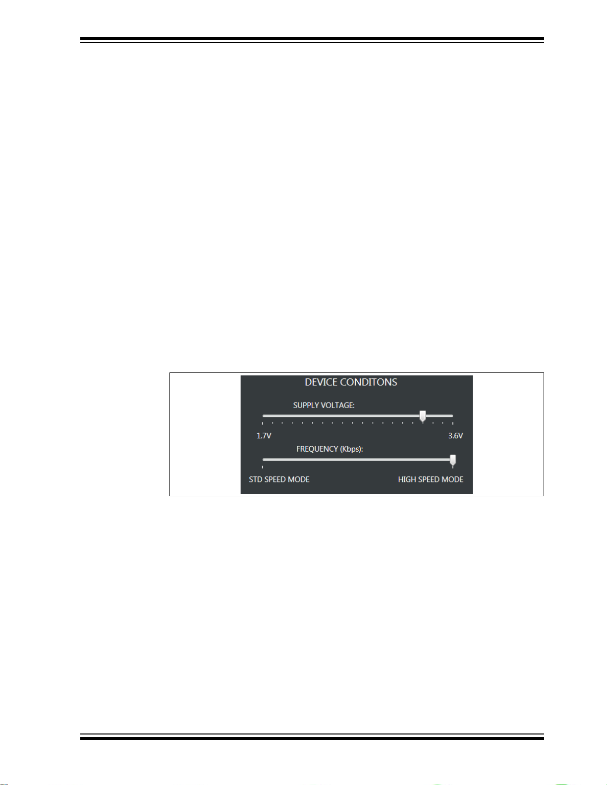
3.5 DEVICE CONDITIONS
The Device Conditions pa ne (Figure 3-6) allows the u ser to set the supply voltage to
the SWI Socket Boa rd and the comm unic ation spe ed or frequenc y of the Si ngle-Wi re
Interface (SWI) protocol.
FIGURE 3-6: DEVICE CONDITIONS PANE
3.5.1 Supply Voltage Slider
The voltage slider provides the ability to change the supply voltage to the SWI Socket
Board along with the installed device V
to pull up the SI/O line. The user can change the V
or dragging the indicator to the desired V
are determined by the installed device specification. Because the supply voltage is
common between every device on the SWI Socket Board, a test point is included to
measure V
PUP to the installed device and VCC supply to the AT24CS02. Whenever the
GUI is initially started, the voltage slider will default to 3.3V to ensure the installed
supported device has sufficient V
PUP voltage. The VPUP refers to the voltage used
PUP by either clicking along the slider
PUP. The upper and lower limits of the VPUP
PUP to communicate.
2018 Microchip Technology Inc. DS20005939A-page 19
Page 20

DM160232 Serial Memory Single-Wire Evaluation Kit User’s Guide
3.5.2 Frequency (Kbps) Slider
The frequency slider provides the ability to change the I/O or communication speed
between the host controller (USB Base Board) and the installed device. The user can
change the I/O speed by either clicking along the slider or dragging the indicator to the
desired I/O speed. The upper and lower frequency limits of the frequency slider are
determined by the installed device specification. Whenever the GUI is initially started,
the frequency slider will default to High-Speed mode to ensure the installed supported
device is able to communicate with the host controller.
Note: The Device Query feature communicates with the Serial EEPROM using
High-Speed mode. Therefore, whenever the Device Query feature is used,
it will revert the installed device back to High-Speed mode regardless of the
current frequency slider setting.
3.6 DEVICE STATUS
The Device Status pane shows various Serial EEPROM device features including the
serial number, the device slave address, the Manufacturer (MFG) ID register, the lock
state of the Security register, and the lock state of the memory zones (Zone 0 -Zone 3)
(Figure 3-7).
FIGURE 3-7: DEVICE STATUS PANE
3.6.1 Serial Number
Displays the serial number read from the Security register of the installed supported
device. The serial number is displayed in hexadecimal.
3.6.2 Slave Address
Displays the preprogrammed device slave address of the installed device. The slave
address is populated with A2 bit first, A1 bit second, and A0 bit last. The slave address
is displayed in binary.
3.6.3 MFG ID Register
Reports the content of the installed device’s Manufacturer ID register. The data is
displayed in hexadecimal.
3.6.4 Security Register User Space
Displays the lock state of the Security register. If the register is not locked, UNLOCKED
is displayed. If the register is locked, LOCKED is displayed.
2018 Microchip Technology Inc. DS20005939A-page 20
Page 21

DM160232 Serial Memory Single-Wire Evaluation Kit User’s Guide
3.6.5 Zone X Lock State
Displays the lock state for the respective memory zones (Zone 0 through Zone 3). If the
zone is not locked, UNLOCKED is displayed. If the zone is locked, LOCKED is
displayed.
3.7 SET DEVICE PROTECTION
The Set Device Protection pane (Figure 3-8) allows the user to independently lock the
four memory zones and the Security register based on the user’s preference. The user
locks a zone or the Security register by pressing the button to the right of that memory
region. The button also indicates the current lock status of that zone or the Security
register and the button shading is based on the current lock status.
pressed, a warning message is displayed to make sure the user intends to lock that
zone or the Security register.
Note: Once the Security register or a memory zone is locked, it cannot be
unlocked and is permanently set to ROM (Read-Only-Memory).
FIGURE 3-8: SET DEVICE PROTECTION PANE
Once a button is
3.8 DEVICE SPECIFICATION
The Device Specification pane (Figure 3-9) displays key device parameters, which can
be found in the installed device’s data sheet. These parameters include “Voltage
Range”, “Frequency Range”, “Endurance Rating”, and “Data Retention”.
FIGURE 3-9: DEVICE SPECIFICATION PANE
2018 Microchip Technology Inc. DS20005939A-page 21
Page 22

DM160232 Serial Memory Single-Wire Evaluation Kit User’s Guide
Clear Log button
Export Log button
Show Legend
checkbox
3.9 T RANSACTION LOG
The Transaction Log records all single-wire communication with the installed device as
well as highlights the communication protocol according to the legend. The Transaction
Log reports the data on the single-wire bus in hexadecimal. The Transaction Log can
be used in conjunction with an oscilloscope connected to the SI/O and GND test points
to help the user decode the captured protocol.
Note: The Transaction Log does not capture the Reset and Discovery Response
sent to the installed device. The Reset and Discovery Response can be
observed by performing a device query while monitoring an oscilloscope
connected to the SI/O and GND test points.
FIGURE 3-10: TRANSACTION LOG
3.9.1 Clear Log
The CLEAR LOG button clears the Transaction Log. The Clear Log function is helpful
when the user wants to look at a specific type or group of single-wire protocol.
3.9.2 Export Log
The EXPORT LOG button exports the Transaction Log in HTML format. The exported
Transaction Log can be used as a reference without having to resend protocol to the
installed device.
3.9.3 Legend
The Transaction Log legend highlights the different data bytes in the single-wire
protocol that is being sent/received; the device address byte is shown in red, the word
address byte is shown in blue, data input by te(s) is shown in green, and data output
byte(s) or the response is shown in black. The Show Legend function can either show
or hide the Transaction Log legend.
2018 Microchip Technology Inc. DS20005939A-page 22
Page 23

DM160232 Serial Memory Single-Wire Evaluation Kit User’s Guide
3.10 GUI MEMORY ARRAY
The GUI memory array is initially populated with the data read from the installed Serial
EEPROM. The data of the GUI memory array is organized in 8-byte rows, left to right,
and in ascending order. The GUI memory array will always be displayed in 8-byte row
lengths regardless of the installed device’s page size. The GUI memory array data
can be modified by the user by using various GUI features which are outlined in the
subsequent sections .
The GUI memory array features memory cell shading that is used to highlight the
different state of that me mory c ell or ce lls. Green shading indicates that the cell or cells
have not been locked and the user can write to that word address or range of word
addresses. Red shading indicates that cell or cells have been locked and now functions
as Read-Only-Memory (ROM). Yellow shading indicates that the memory array cell or
cells have been changed in the internal GUI buffer and have not been written to the
Serial EEPROM (see Section 3.11.5 “PROGRAM” for additional information).
FIGURE 3-11: MEMORY ARRAY
When the user hovers the mouse cursor over the GUI memory array, a pop-up appears
to show the data in HEX, data in ASCII, Address, Zone: #, and Zone Protection state
of that particular memory cell. This is illustrated in Figure 3-12.
FIGURE 3-12: ARRAY HOVER
The user can change the content of a cell by double-clicking a word address or memory
cell in the GUI memory array or GUI Security register (see Figure 3-13). In order to
change the content of a cell, the user should update the value, followed by pressing the
Update Cell button. Once the cell is updated, the cell shading will become yellow. This
indicates to the user that they must then program the device using the Program Feature
(see Section 3.11.5 “PROGRAM” for additional information).
2018 Microchip Technology Inc. DS20005939A-page 23
Page 24

DM160232 Serial Memory Single-Wire Evaluation Kit User’s Guide
Update Cell
button
Hex button
ASCII button
Load button
Save button
Program button
Refresh button
FIGURE 3-13: ARRAY UPDATE CELL
3.11 ARRAY ACTIONS
Array actions allow the user to manipulate the GUI memory array in terms of how the
data is displayed (HEX or ASCII) and also allow the user to save the GUI memory array
or load a previous array.
FIGURE 3-14: ARRAY ACTIONS
2018 Microchip Technology Inc. DS20005939A-page 24
3.11.1 HEX
The HEX button displays the GUI memory array in hexadeci ma l (HE X) form at.
3.11.2 ASCII
The ASCII button displays the GUI memory array in American Standard Code for
Information Interchange (ASC II) forma t.
3.11.3 LOAD
The LOAD button gives the user the option to load a previous saved GUI memory array
either HEX (.hex) or TEXT (.txt) file. The file, once loaded, will be used to populate the
internal GUI buffer. Once the file is loaded in the GUI array buffer, the user must
program the installed device using the PROGRAM button (see
Section 3.11.5 “PROGRAM” for additional information).
Note: The loaded file must follow a specific format. In order to determine the
correct file format, it is recommended to save a GUI memory array as a
reference (see Section 3.11.4 “SAVE” for additional information) and refer
to that file when formatting the data.
Page 25

DM160232 Serial Memory Single-Wire Evaluation Kit User’s Guide
File type selection
buttons
FIGURE 3-15: LOAD
3.11.4 SAVE
The SAVE button gives the user the ability to save the current state of the GUI memory
array. The GUI memory array can be saved as either a HEX (.hex) file or TEXT (.txt)
file based on the user preference. Once a file type is selected, a file explorer will pop
up prompting the user to specify the file directory and name of the file.
Note: When using the Save feature, the software will create the data for the saved
file based on the internal GUI buffer and not on the actual data from the
Serial EEPROM.
FIGURE 3-16: SAVE
3.11.5 PROGRAM
The Program feature can be used to write to the Serial EEPROM memory array,
Security register, lock Zone 0 to Zone 3, and lock the Security register. When the
PROGRAM button is pressed, the current internal GUI buffer will be written to the Serial
EEPROM memory. The Program feature must be used when a cell is updated
(yellow shaded), or when a file (.hex or .txt) is loaded. If the Program feature is not
used, the data in the internal GUI buffer will not be written to the Serial EEPROM.
The Program feature can also be used to lock the four memory zones and/or the
Security register. Each zone and the Security register can be locked independently of
each other by placing a check mark in the corresponding box.
When the Program feature is used to program the Serial EEPROM memory array or
Security register, that entire memory region will be written with the current data in the
internal GUI buffer rather than only the changed values. If a specific data byte or bytes
are to be programmed, it is recommended to use the Write feature
(see Section 3.13.2 “Write” for additional information).
Note: By default, the memory array is selected. Therefore, if the user only wants
to write the Security register or lock a zone or register, the user must
unselect the memory array and select the particular operation to be
performed.
2018 Microchip Technology Inc. DS20005939A-page 25
Page 26

DM160232 Serial Memory Single-Wire Evaluation Kit User’s Guide
Write checkboxes
Lock checkboxes
Refresh status bar
FIGURE 3-17: PROGRAM
3.11.6 REFRESH
The REFRESH button reads the Serial EEPROM memory array and Security register
of the installed device and then populates the GUI memory array and Security register
with that data. If there is data in the internal GUI buffer (yellow-shaded cell) when the
Refresh feature is used, that data will be replaced with the data read from the Serial
EEPROM. After the completion of any write operation to the Serial EERPOM, the GUI
will automatically update the GUI memory array and Security register using the Refresh
feature.
Note: If a new device is installed while leaving the USB Base Board connected to
the user’s PC, it is recommended to use the Device Query feature instead
of the Refresh feature to ensure robust GUI operation.
FIGURE 3-18: REFRESH
3.12 SECURITY REGISTER
The Security register consists of a factory-programmed unique serial number in the
lower 8 bytes (address 0x00h to 0x07h), an 8-byte page that is reserved for future use
with data of 0xFFh (address 0x08 to 0x0F), and a writable portion in the upper 16 bytes
(address 0x10h to 0x1Fh) of the Security regis ter. Th e red-shaded ce ll s indi cate they
are locked and cannot be modified by the user; green-shaded cells indica te that the cel l
or cells are unlocked and can be modified by the user; yellow shading indicates that the
memory array cell or cells have been changed in the internal GUI buffer and have not
been written to the Serial EEPROM.
2018 Microchip Technology Inc. DS20005939A-page 26
Page 27

DM160232 Serial Memory Single-Wire Evaluation Kit User’s Guide
The entire Security register can be locked by either using the Program feature (see
Section 3.11.5 “PROGRAM”) or using the Set Device Protection pane (see
Section 3.7 “Set Device Protection”).
Note: Once the Security register has been locked, it cannot be unlocked and is
permanently set to ROM (Read-Only-Memory).
FIGURE 3-19: SECURITY REGISTER
3.13 ARRAY BUTTONS
The array buttons, which are located below the GUI Security register, allow the user to
perform read and write operations to the Serial EEPROM, use the Go To Address
feature to highlight a specific word address in the GUI memory array, and also provides
various support functions.
FIGURE 3-20: ARRAY BUTTONS
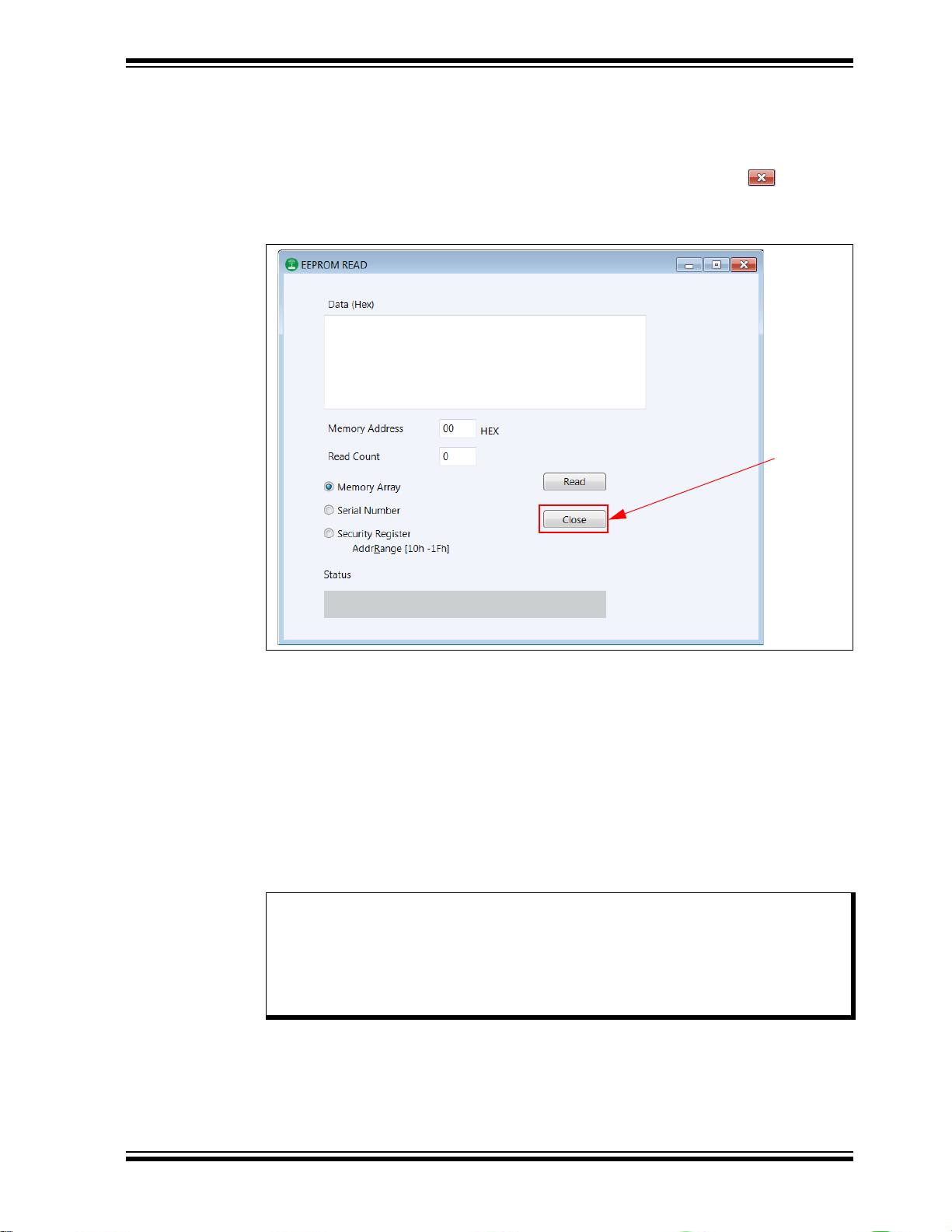
3.13.1 Read
The Read feature allows the user to read the entire Serial EEPROM memory array, a
specific word address or a range of word addresses, the serial number, and/or the
Security register of the Serial EEPROM. When the READ button is pressed, a pop-up
window appears allowing the user to enter details related of the read operation to be
performed.
Note: The Read feature will not update the GUI memory array or GUI Security
register. To update the GUI, use the Refresh feature (see the
Section 3.11.6 “REFRESH”for additional information).
The user can input a starting word address using the Memory Address field that the
read operation will start at (in hexadecimal), the Read Count or the amount of bytes to
be read, and the user can select what read operation is to be performed (Memory
Array, Serial N umber, or Security Register). Once all the input data has been filled,
press the READ button to start the read operation. A status message is included at the
bottom of the window to notify the user that the read operation is complete by displaying
“Successful”.
Note: If the user performs a read operation to the Security register or reads the
serial number, the GUI will automatically populate the starting memory
address for the user stating at the first byte of either the writable portion
(upper 16 bytes) of the Security register or the serial number depending on
which is selected. The user can change the starting address, but the GUI
will limit the word address to the Security register boundaries.
2018 Microchip Technology Inc. DS20005939A-page 27
Page 28
DM160232 Serial Memory Single-Wire Evaluation Kit User’s Guide
Close
button
Once the read operation is complete, the data will be displayed in hexadecimal in the
Data (Hex) field. The user can perform as many read operations as preferred from this
window. For each new read operation, the Data field will be re-written using the data
read from the current read operation being performed. Once all read operations are
completed, the user can close the window by pressing the red button ( ) in the top
right hand corner of the pop-up window or pressing the Close button.
FIGURE 3-21: READ OPERATION
3.13.2 Write
The Write feature allows the user to write the entire Serial EEPROM memory array, a
specific word address or a range of word addresses, and the writable portion of the
Security register. When the WRITE button is pressed, a pop-up window appears
allowing the user to enter details related to the write operation to be performed.
The user inputs the data that is to be written in the Data field (in hexadecimal). The user
then selects the starting word address using the Memory Address (hex) field that the
write operation will start at (in hexadecimal). The Count, or the number of bytes to be
written, is filled automatically based on the amount of data bytes in the “Data” field. The
user can also select whether the write operation will occur in the Serial EEPROM
memory array or the Security register.
Note: If the user performs a write operation to the Security register, the GUI will
automatically populate the memory address for the user stating at the first
byte of the writable portion (upper 16 bytes) of the Security register. The
user can change the starting word address of the write operation, but the
GUI limits the word address to the writable portion (upper 16 bytes) of the
Security register.
The GUI limits write operations to the physical device boundary (address of 0x7Fh for
the memory array and address of 0x1Fh for the Security register).The write operation
will be aborted if the address boundary of that particular memory region is exceeded.
2018 Microchip Technology Inc. DS20005939A-page 28
Page 29

DM160232 Serial Memory Single-Wire Evaluation Kit User’s Guide
Close button
Once all the input data has been input, press the WRITE button to start the write
operation. A status message is included at the bottom of the window to notify the user
that the write operation is complete by displaying “Successful”.
Note: Due to the construction of the Serial EEPROM devices, the write operation
is limited to the page size or boundary of the installed device. If the “Data”
field exceeds the page boundary of the installed device, the GUI will
automatically parse the data into the correct page size and perform multiple
write operations until the entire data field has been written to the Serial
EEPROM.
Once the entire write operation is complete, the user can close the window by pressing
the red button ( ) in the top right-hand corner of the pop-up window or pressing the
Close button. Once either is pressed, a progress bar for the Refresh feature is
displayed and the entire GUI memory array and Security register are read and the GUI
is updated accordingly.
FIGURE 3-22: WRITE OPERATION
3.13.3 Go To Address
The Go To Address feature allows the user to jump to a specific word address in the
GUI memory array. Once the Go To Address button is pressed, the memory address
that was input will be highlighted in a black box in the GUI memory array.
Note: The Go T o Address feature does not work for the GUI Security register and
only works for addresses within the GUI memory array.
FIGURE 3-23: GO TO ADDRESS
2018 Microchip Technology Inc. DS20005939A-page 29
Page 30

DM160232 Serial Memory Single-Wire Evaluation Kit User’s Guide
3.13.4 Other Actions
The OTHER ACTIONS button is reserved for future use (RFU) if future GUI
enhancements are made.
3.13.5 Support
The SUPPORT button provides a hyperlink to various support pages. The support
feature allows the user to select between three support classes.
• “Contact Support” which directs the user to the Microchip support portal
• “Order more Samples” which directs the use to microchipDIRECT
• “Find other Devices” which directs the user to Microchip Serial EEPROM memory
page
FIGURE 3-24: SUPPOR T
2018 Microchip Technology Inc. DS20005939A-page 30
Page 31

Chapter 4. USB Base Board Firmware Upgrade
Install
button
4.1 INTRODUCTION
The Microchip Technology Serial Memory Evaluation Kits have a built-in ability to
upgrade the USB Base Board using a sequence of steps along with using the Atmel
FLexible In-system Programming (FLIP) software.
The following steps are needed to successfully install the FLIP Software Utility:
1. Go to http://www.microchip.com/DM160232 to download the FLIP Software
Utility
2. Navigate to Documentation and Software and select the FLIP Software Utility.
DM160232 SERIAL MEMORY
SINGLE-WIRE EVALUATION KIT
USER’S GUIDE
3. Download and open the setup file
JRE - Flip Installer - x.x.x.xxx.exe (x.x.x.xxx indicates the version)
4. Once the setup file is opened, if Java Runtime is already installed or a newer
version is already installed, the setup will automatically start and you may skip to
Step 8. If no Java Runtime or an older version is present on the user’s PC, when
prompted, press the Install button to start the Java Runtime installation.
Note: If prompted, allow the program to make changes to your PC.
FIGURE 4-1: JAVA RUNTIME ENVIRONMENT SETUP
.
2018 Microchip Technology Inc. DS20005939A-page 31
Page 32

DM160232 Serial Memory Single-Wire Evaluation Kit User’s Guide
Close
button
Setup
button
Accept button
5. Let the program setup the Java Runtime. A progress or status bar is included to
show the overall progress of the installation. Once completed, press the Close
button.
FIGURE 4-2: JAVA RUNTIME INSTALLATION
6. When prompted, select “Typical setup” and press the Accept button to accept
the License Agreement.
Note: For this example, the Typical setup was used. If the user selects a Custom
setup, it is the user’s responsibility to ensure the FLIP Software Utility is
installed correctly.
FIGURE 4-3: JAVA RUNTIME TYPICAL SETUP
2018 Microchip Technology Inc. DS20005939A-page 32
Page 33

DM160232 Serial Memory Single-Wire Evaluation Kit User’s Guide
Finish
button
Next
button
7. Let the program setup the Java Runtime. A progress or status bar is included to
show the overall progress of the installation. Once completed, press the Finish
button to complete the Java Runtime installation.
FIGURE 4-4: JAVA RUNTIME COMPLETION
8. Once the Java Runtime is installed, the FLIP Setup Wizard is automatically
started. Once ready, click the Next button to continue.
FIGURE 4-5: FLIP SETUP WIZARD
2018 Microchip Technology Inc. DS20005939A-page 33
Page 34

DM160232 Serial Memory Single-Wire Evaluation Kit User’s Guide
“I accept”
checkbox
Next button
Next
button
9. Read the License Agreement. When finished, accept the terms in the License
Agreement by checking the box and press the Next button to continue.
FIGURE 4-6: FLIP LICENSE AGREEMENT
10. The next step is to select the installation location. The default installation location
is set to C:\Program Files (x86)\Atmel\Flip x.x.x (x.x.x indicates
the version). It is recommended that the default installation location is used.
Once the installation location has been selected, press the Next button.
FIGURE 4-7: FLIP INSTALLATION LOCATION
2018 Microchip Technology Inc. DS20005939A-page 34
Page 35

DM160232 Serial Memory Single-Wire Evaluation Kit User’s Guide
Install
button
Finish
button
1 1. The next step is to choose a Start Menu folder. By default, the Start Menu folder
is set to Flip x.x.x, where x.x.x indicates the FLIP version. It is recommended that
the default Start Menu folder is used. Once ready, press the Install button to
continue.
FIGURE 4-8: FLIP START MENU FOLDER
12. Let the program setup the FLIP Software Utility. A progress or status bar is
included to show the overall progress of the installation. Click the Next button
during the installation progress, if prompted. Once completed, press the Finish
button to complete the FLIP Software Utility installation.
FIGURE 4-9: FLIP SOFTWARE UTILITY COMPLETE
2018 Microchip Technology Inc. DS20005939A-page 35
Page 36

DM160232 Serial Memory Single-Wire Evaluation Kit User’s Guide
4.2 INSTALLING THE GRAPHICAL USER INTERFACE (GUI)
Once the FLIP Software Utility has been successfully installed on the user’s PC, the
next step is to download and install the latest version of the DM160232 SWI Graphical
User Interface (GUI) software.
The following steps are necessary to successfully install the GUI software:
1. Go to http://www.microchip.com/DM160232 to download the GUI software.
2. Navigate to “Documentation and Software” and select the “DM160232 SWI GUI
software”.
3. Download and open the setup file.
DM160232_x.x.x_setup.exe (x.x.x indicate the GUI version)
4. Install the GUI using the procedure outlined in Section 2.3 “Installing the
Graphical User Interface (GUI)”.
Note: If an earlier version of the SWI GUI was previously installed, it is recom-
mended to uninstall the previous version before installing the new version.
This will ensure robust GUI operation.
4.3 USB BASE BOARD DFU MODE
Once the latest version of the GUI has been installed on the user’s PC, the next step
is to plug in the USB Base Board into a USB port without the SWI Socket Board
connected. The PC will recognize the USB Base Board as “AVR MEGA Virtual Com
Port” in the PC’s Devices and Printers window from the Control Panel if there is
firmware already loaded in the USB Base Board (Figure 4-10). Note that the COM port
numeration may change based on the user’s PC.
FIGURE 4-10: AVR MEGA VIRTUAL COM PORT
2018 Microchip Technology Inc. DS20005939A-page 36
Page 37
DM160232 Serial Memory Single-Wire Evaluation Kit User’s Guide
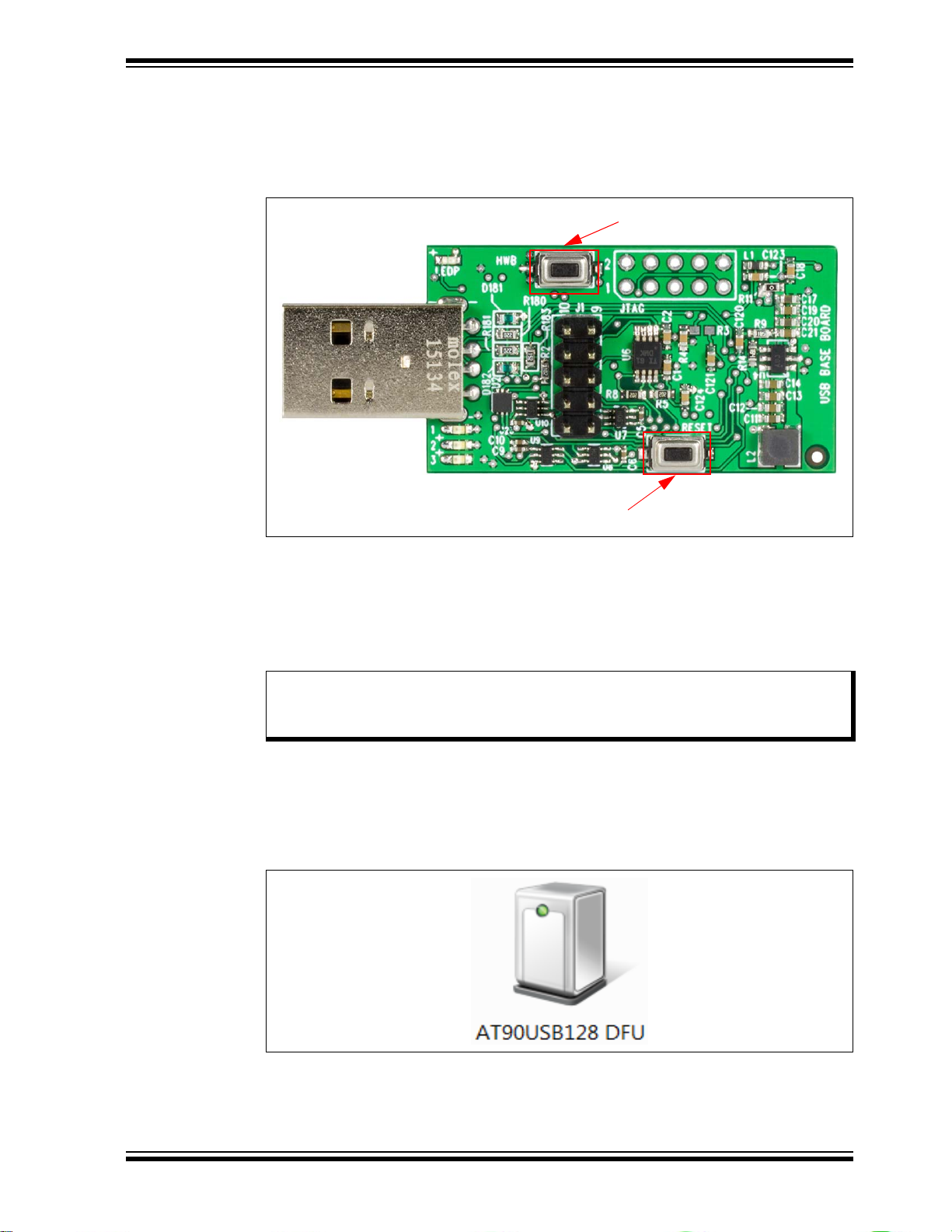
HWB button
RESET button
Once the USB Base Board is plugged in and recognized by the PC, the user should
enable DFU mode on the USB Base Board. DFU mode is enabled by a specific
sequence of HWB and RESET buttons. Refer to Figure 4-11 for locations of the HWB
and RESET buttons.
FIGURE 4-11: USB BASE BOARD BUTTONS
Once the HWB and RESET buttons have been located, use the specific press and hold
sequence shown below to enable DFU mode on the USB Base Board.
• Press and hold the HWB button
• Press and release the RESET button
• Release the HWB button
Note: Once DFU mode is enabled on the USB Base Board, the rest of the
firmware upgrade process must be completed in order to ensure robust
USB Base Board operation.
Once the USB Base Board has DFU mode enabled, allow the PC to relearn the USB
Base Board as “AT90USB128 DFU” (Figure 4-12). If the PC does not automatically
recognize the USB Base Board as stated above and shown below, it is recommended
to unplug the USB Base Board from the PC and restart the procedure.
FIGURE 4-12: AT90USB128 DFU COM PORT
2018 Microchip Technology Inc. DS20005939A-page 37
Page 38

DM160232 Serial Memory Single-Wire Evaluation Kit User’s Guide
4.4 FLIP SOFTWARE UTILITY
Once the USB Base Board has DFU mode enabled and the COM port is relearned by
the PC, perform the following sequence using the FLIP Software Utility to upgrade the
USB Base Board firmware.
1. Open the FLIP Software Utility (Figure 4-13) by either selecting the desktop icon
(if created) or selecting “Flip x.x.x” (x.x.x indicates the version) from the Start
Menu folder.
FIGURE 4-13: FLIP SOFTWARE UTILITY
2. After opening the FLIP Software Utility, navigate to the Device Selection icon as
shown below. Select the “AT90USB1287” as the device and press the OK button.
2018 Microchip Technology Inc. DS20005939A-page 38
Page 39

DM160232 Serial Memory Single-Wire Evaluation Kit User’s Guide
Device
Selection icon
AT90USB1287
FIGURE 4-14: DEVICE SELECTION
2018 Microchip Technology Inc. DS20005939A-page 39
Page 40

DM160232 Serial Memory Single-Wire Evaluation Kit User’s Guide
Communication
Medium icon
USB
File
Load HEX Files
3. Once the target device has been selected, click on the Communication Medium
icon as shown below and select “USB”. Once “USB” is selected, an additional
dialog box is displayed. Press the Open button to continue.
FIGURE 4-15: COMMUNICATION MEDIUM SELECTION
4. Once the communication between the PC and the AT90USB1287 (USB Base
Board microcontroller) has been established, navigate to File and select “Load
HEX Files” as shown in Figure 4-16.
FIGURE 4-16: LOAD FILE
2018 Microchip Technology Inc. DS20005939A-page 40
Page 41

DM160232 Serial Memory Single-Wire Evaluation Kit User’s Guide
Run button
Verify PASS
message
5. Proceed to load the SWI firmware. Navigate to the firmware found at:
C:\Program Files (x86)\Microchip\Serial Memory Evaluation
Kits\Single-Wire\Firmware
Note: If the default installation was not used when the DM160232 SWI GUI was
installed, it is the user’s responsibility to determine the SWI firmware file
location.
6. Once the HEX file has been loaded into the FLIP Software Utility , press the Run
button to program the new firmware to the AT90USB1287 as shown below. A
progress or status bar is included to show the overall progress of the hex image
program.
FIGURE 4-17: RUN FLIP SOFTWARE
7. If the “Verified Pass” is reported in the FLIP Software Utility (see Figure 4-18),
close the FLIP Software Utility and remove the USB Base Board from the PC.
The USB Base Board Firmware Upgrade procedure is complete.
Note: If the USB Base Board was updated successfully, the PC will recognize the
USB Base Board as “AVR MEGA Virtual Com Port” (see Figure 4-10).
If the “Verified Pass” is not shown, or any other error is displayed, it is
recommended to unplug the USB Base Board from the PC and restart the entire
firmware upgrade procedure.
FIGURE 4-18: FLIP SOFTWARE COMPLETE
2018 Microchip Technology Inc. DS20005939A-page 41
Page 42

DM160232 SERIAL MEMORY
SINGLE-WIRE EVALUATION KIT
USER’S GUIDE
Chapter 5. Troubleshooting Guide
ISSUE: USB BASE BOARD IS NOT RECOGNIZED BY THE USER’S PC
SOLUTION:
ISSUE: GUI STATES THE USER MUST PERFORM A FIRMWARE UPDATE
SOLUTION: Perform the USB Base Board Firmware Upgrade using the procedure outlined in
The USB Base Board driver is not installed or not installed properly. Download and
install the USB Base Board driver using the procedure outlined in
Section 2.2 “Installing the USB Base Board Driver”.
The USB Base Board firmware was not programmed properly or has become
corrupted. Perform the USB Base Board Firmware Upgrade using the procedure
outlined in Chapter 4. “USB Base Board Firmware Upgrade”.
TO THE USB BASE BOARD
Chapter 4. “USB Base Board Firmware Upgrade”.
ISSUE: GUI STATES THERE IS NO DEVICE INSTALLED IN THE SWI
SOCKET BOARD
SOLUTION: Close the GUI and remove the USB Base Board from the PC. Verify that the SWI
Socket Board and the USB Base Board are connected properly. Also verify that the
device is installed correctly in the SOT23 socket on the SWI Socket Board. Refer to
Section 2.4 “Evaluation Kit Setup Procedure” for additional information. Make sure
the socket lid is shut without any binding. Plug the SWI Socket Board into the USB
Base Board and restart the GUI. If the problem persists, contact your local Sales
representative for additional support or create a support ticket at
www.microchip.com/support.
2018 Microchip Technology Inc. DS20005939A-page 42
Page 43

DM160232 Serial Memory Single-Wire Evaluation Kit User’s Guide
NOTES:
2018 Microchip Technology Inc. DS20005939A-page 43
Page 44

A.1 INTRODUCTION
This appendix contains the following schematics for the DM160232 Serial Memory
Single-Wire Evaluation Kit:
• SWI Socket Board (02-10681)
• USB Base Board (02-10682)
Note: Electronic versions of the SWI Socket Board and USB Base Board sche-
DM160232 SERIAL MEMORY
SINGLE-WIRE EVALUATION KIT
USER’S GUIDE
Appendix A. Schematics
matics can be downloaded from http://www.microchip.com/DM160232
under “Documentation and Software”.
2018 Microchip Technology Inc. DS20005939A-page 44
Page 45
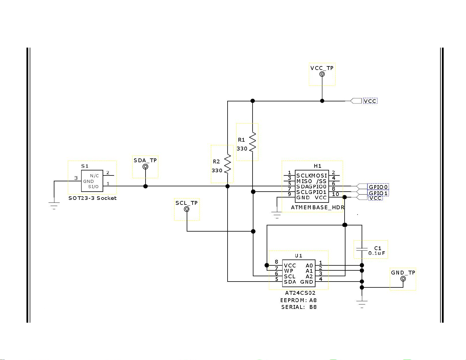
2018 Microchip Technology Inc. DS20005939A-page 45
A.2 SWI SOCKET BOARD (02- 10681)
DM160232 Serial Memory Single-Wire Evaluation Kit User’s Guide
Page 46

2018 Microchip Technology Inc. DS20005939A-page 46
PROCESSOR
USB
RESET MEB
BOOTLOADER
JTAG
CONNECTOR PORT
Oscillator
+5V
3.3V POWER CIRCUIT
VCCB: CONTROLLER SIDE
DAC & U NITY G AIN AMP LIFIER
Reroute u5 power connection
VCCA: DUT SIDE
VCCA <= VCCB
16 ADC
Note: V CC also serve s as Vref
LEVE L SHIFTE R
VCCA [0.8V to 5.5V]
VCCB [2.2 V to 5.5V]
VCCA <= VCCB
MCP16251
1
2
C123
0.1uF
1
2
C121
0.1uF
1
2
C120
0.1uF
1
PE6
2
PE7
3
UVCC
4
D-
5
D+
6
UGND
7
UCAP
8
VBUS
9
PE3
10
PB0
11
PB1
12
PB2
13
PB3
14
PB4
15
PB5
16
PB6
17
PB718PE419PE520RESET_21VCC22GND23XTAL224XTAL125PD026PD127PD228PD329PD430PD531PD632PD7
33
PE0
34
PE1
35
PC0
36
PC1
37
PC2
38
PC3
39
PC4
40
PC5
41
PC6
42
PC7
43
PE2
44
PA7
45
PA6
46
PA5
47
PA4
48
PA3
49
PA250PA151PA0
52
VCC
53
GND
54
PF755PF656PF557PF458PF359PF260PF161PF0
62
AREF
63
GND
64
AVCC
65
IC2
AT90USB1287-64QFN
2
1
C124
0.1uF
1
SCLK
3
MISO
5
SDA
7
SCL
9
GND
2
MOSI
4
/SS
6
GPIO0
8
GPIO1
10
VCC
J1
ATMEMBASE_HDR
1
3
5
7
2
4
6
8
910
JTAG
10POS .100 MALE HDR
C117
0.1uF
1
2
C126
20pF
1
2
C125
20pF
1A12
B1
RESET
PUSH_BTN
R151
47K
1
2
C151
0.1uF
C184
0.1uF
R184
47K
1A12
B1
HWB
PUSH_BTN
D182
TVS DIODE
1
2
3
4
USB
USB
R180
22
D181
TVS DIODE
R183
1.5K
R181
22
LEDP
1
2
R144
4.7K
1
1
2
R103
825
2
1
2
R104
825
1
2
3
4
Y121
16MHz Xtal
3
1
2
R105
825
1
2
R6
180
1
2
R7
180
12
L1
10uH
1
2
R3
DNI
1
2
R4
0.1uF
1
VCC
2
VIN
3
GND4CS
5
SDO
6
SCK
7
CPAD
U2
LTC2450
1
VDD
2
CS
3
SCK
4
SDI5LDAC
6
VREF
7
VSS
8
VOUT
U3
MCP4921T-E/MS
1
2
C15
0.1uF
1
2
C16
0.1uF
1
2
C18
0.1uF
C101
1.0uF
C102
1.0uF
C103
10uF
1
VIN
2
GND
3EN4
BYPASS
5
OUT
U1
576-1281-1-ND
1
OUTA
2
V-
3
+INA4-INA
5
V+
U5
1
VCCA
2
SCLA
3
SDAA
4
GND
5
EN
6
SDAB
7
SCLB
8
VCCB
U6
TCA9617A_8-SSOP
1
2
C2
0.1uF
1
2
C3
0.1uF
1
2
C4
0.1uF
1
2
R2
1K
1
2
R8
2K
1
2
R5
2K
1
2
R12
DNI
1
2
R13
0
1
VCCA
2
A
3
GND4EN
5
Y
6
VCCY
U7
1
VCCA
2
A
3
GND4EN
5
Y
6
VCCY
U8
1
VCCA
2
A
3
GND4EN
5
Y
6
VCCY
U9
C5
1.0uF
C6
1.0uF
C7
1.0uF
C8
1.0uF
C9
1.0uF
C10
1.0uF
1
2
C1
0.1uF
R1
1.5
3
EN
2
GND
1
SW
4
FB
5
VOUT
6
VBAT
U4
12
L2
4.7uH
1
2
R9
499K
1
2
R14
143K
C11
4.7uF
C12
4.7uF
C13
4.7uF
C14
4.7uF
C17
4.7uF
C19
4.7uF
C20
4.7uF
C21
4.7uF
R11
0
1
VCCA
2
A
3
GND4EN
5
Y
6
VCCY
U10
C22
1.0uF
C23
1.0uF
1
2
R10
0
1
FD1
FIDUCIAL_PAD
1
FD2
FIDUCIAL_PAD
1
FD3
FIDUCIAL_PAD
1
FD4
FIDUCIAL_PAD
DP_USB
DM_USB
PE4
SDA
SCL
VCC
RESET_MEB
VCC
VCC
MISO
MOSI
SCLK
SS
VCC
GPIO1
GPIO0
SS_DUT
SCL_DUT
SDA_DUT
MISO_DUT
VCC
VCC
VCC
RESET_MEB
DP_USB
DM_USB
PE4
HWB
HWB
5V5
SCLK_DUT
DUT_VCC
XTAL1
XTAL2
GPIO0
MOSI_DUT
XTAL1
XTAL2
TCK
TDO
TMS
TDI
TCK
TMS
TDO
TDI
VCC
GND
GND
VCC
SCLK
MISO
ADCCS
GPIO1
ADCCS
VCC
MOSI
SCLK
CS_DAC
/LDAC
VUSB
CS_DAC
DUT_VCC
VCC
/LDAC
GPIO1
DUT_VCC
SCL
SDA
DUT_VCC
VCC
3V3
5V5
3V3
VCC
DUT_VCC
SCLK_DUT
MISO_DUT
MOSI_DUT
SCLK
MISO
MOSI
VCC
SCL_DUT
SDA_DUT
VUSB
VCC
SS_DUT
SS
A.3 USB BASE BOARD (02-10682 )
DM160232 Serial Memory Single-Wire Evaluation Kit User’s Guide
Page 47

DM160232 SERIAL MEMORY
SINGLE-WIRE EVALUATION KIT
USER’S GUIDE
Appendix B. Bill of Materials (BOM)
TABLE B-1: SWI SOCKET BOARD (02-10681)
Qty Reference Description Manufacturer Part Number
1 C1 Ceramic Capacitor, 0.1 µF, 50V, 20%
X5V SMD 0603
1 H1 Receptacle Connector, 100",
10 positions Dual Gold
1 PCB Printed Circuit Board – DM160232 SWI
Socket Board
2 R1, R2 Resistor-SMD, 330 Ohms, 5%, 1/10W,
0603
1 S1 3-lead SOT23 Socket Sensata Technologies
4 T1, T2, T3, T4 PC Test Point, Compact SMT Keystone Electronics
1 U1 Atmel 2 Kb Serialized 2-wire device
SOIC-8
1 SOCKET Installed Atmel 1 Kb Serialized SWI
device SOT23
4 N/A Loose Atmel 1 Kb Serialized SWI device
SOT23
Note 1: The components listed in this Bill of Mate rials are repre senta tive of the PC B assembly. The released BOM
used in manufacturing uses all RoHS-compliant components.
(1)
Yageo Corporation CC0603ZRY5V9BB104
Samtec Inc. SSW-105-01-F-D
Microchip Technology
Inc.
Yageo Corporation RC0603JR-07330RL
(Wells-CTI)
Corp.
Microchip Technology
Inc.
Microchip Technology
Inc.
Microchip Technology
Inc.
01-10681
499-P36-20
5018
AT24CS02-SSHM-T
AT21CS01-STUM10-T
AT21CS01-STUM10-T
T ABLE B-2: USB BASE BOARD (02-10682)
Qty Reference Description Manufacturer Part Number
3 1, 2, 3 LED RED CLEAR 0603 SMD Lite-On
15 C1, C2, C3, C4,
C15, C16, C18,
C117, C120, C121,
C123, C124, C151,
C184, R4
10 C5, C6, C7, C8, C9,
C10, C22, C23,
C101, C102
8 C11, C12, C13,
C14, C17, C19,
C20, C21
1 C103 Ceramic capacitor, 10 µF, 6.3V
Note 1: The components listed i n this Bill of M ateria ls are re present at ive of the PC B assem bly. The released BOM
used in manufacturing uses all RoHS-compliant components.
2018 Microchip Technology Inc. DS20005939A-page 47
Ceramic capacitor, 0.1 µF, 50V
Y5V 0603
Ceramic capacitor, 1 µF, 6.3V
X5R 0402
Ceramic capacitor, 4.7 µF, 6.3V
X5R 0603
X5R 0603
(1)
®
Technology
Corporation
Yageo Corporation CC0603ZRY5V9BB104
Taiyo Yuden Co., Ltd. JMK105BJ105KV-F
Taiyo Yuden Co., Ltd. JMK107BJ475KA-T
Taiyo Yuden Co., Ltd. JMK107BJ106MA-T
LTST-C191KRKT
Page 48

DM160232 Serial Memory Single-Wire Evaluation Kit User’s Guide
TABLE B-2: USB BASE BOARD (02-10682) (CONTINUED)
Qty Reference Description Manufacturer Part Number
2 C125, C126 Ceramic capacitor, 20 pF, 250V
C0G/NP0 0603
2 D181, D182 TVS Diode, 24VWM 150VC
0603
2 HWB, RESET Tactile switch SPST-NO 0.05A
12V
1 IC2 IC 8-bit MCU, 128 KB, Flash
64QFN
1 J1 Connector – Header, 100" Dual
STR, 10 positions
3 JTAG, R12, R3 DO NOT POPULATE
1 L1 Fixed inductor, 10 µH, 50 mA,
900 MOHM SMD
1 L2 Fixed inductor, 4.7 µH, 1.2A
105 MOHM
1 LEDP LED Blue Diffused, 0603 SMD Osram Opto
1 PCB Printed Circuit Board –
DM160232 USB Base Board
1 R1 Resistor SMD 1.5 Ohm, 5%,
1/10W 0603
1 R2 Resistor SMD 1K Ohm, 5%,
1/10W 0603
2 R5, R8 Resistor SMD 2K Ohm, 5%,
1/10W 0603
2 R6, R7 Resistor SMD 180 Ohm, 5%,
1/10W 0603
1 R9 Resistor SMD 499K Ohm, 1%,
1/10W 0603
2 R10 , R1 1 Resistor SMD 0 .0 Ohm Jumper,
1/10W 0603
1 R 13 Resistor SMD 0.0 Ohm Jumper,
1/16W 0402
1 R14 Resistor SMD 143K Ohm, 1%,
1/10W 0603
3 R103, R104, R105 Resistor SMD 825 Ohm,1%,
1/10W 0603
1 R144 Resistor SMD 4.7K Ohm, 5%,
1/10W 0603
2 R151, R184 Resistor SMD 47K Ohm, 1%,
1/10W 0603
2 R180, R181 Resistor SMD 22 Ohm, 5%,
1/10W 0603
1 R183 Resistor SMD 1.5K Ohm, 5%,
1/10W 0603
1 U1 Linear Regulator IC 3.3V, 0.5A,
SOT23-5
Note 1: The components listed i n this Bill of M ateria ls are re present at ive of the PC B assem bly. The released BOM
used in manufacturing uses all RoHS-compliant components.
Johanson Technology, Inc. 251R14S200GV4T
Littelfuse
Apem, Inc. ADTSM31NV
Microchip Technology Inc.
Sullins Connector
Solutions
Murata Electronics North
America, Inc.
Wurth Electronics Inc. 744031004
Semiconduc tors GmbH
Microchip Technology Inc. 01-10682
Yageo Corporation RC0603JR-071R5L
Yageo Corporation RC0603JR-071KL
Yageo Corporation RC0603JR-072KL
Yageo Corporation RC0603JR-07180RL
Yageo Corporation RC0603FR-07499KL
Yageo Corporation RC0603JR-070RL
Yageo Corporation RC0402JR-070RL
Yageo Corporation RC0603FR-07143KL
Yageo Corporation RC0603FR-07825RL
Yageo Corporation RC0603JR-074K7L
Yageo Corporation RC0603FR-0747KL
Yageo Corporation RC0603JR-0722RL
Yageo Corporation RC0603JR-071K5L
Microchip Technology Inc.
(1)
®
Inc. PGB1010603MR
AT90USB1287-MU
PRPC005DAAN-RC
LQM18FN100M00D
LB Q39G-L2OO-35-1
MIC5219-3.3YM5-TR
2018 Microchip Technology Inc. DS20005939A-page 48
Page 49

DM160232 Serial Memory Single-Wire Evaluation Kit User’s Guide
TABLE B-2: USB BASE BOARD (02-10682) (CONTINUED)
Qty Reference Description Manufacturer Part Number
1 U2 IC ADC 16-bit Sigma-Delta
6-DFN
1 U3 IC DAC 12BIT SNGL W/SPI
8-MSOP
1 U4 Boost regulator adjustable IC
0.65A SYNC SOT23
1 U5 IC OPAMP GP 3 MHz RRO
SOT23-5
1 U6 IC V-Level XLATR FM+ I2C
8-VSSOP
4 U7, U8, U9, U10 Translator bidirectional SGL LL
SC70-6
1 USB Plug connector USB,
4 positions, right angle PCB
1 Y121 Crystal 16.0000MHz, 18 pF
SMD
Note 1: The components listed i n this Bill of M ateria ls are re present at ive of the PC B assem bly. The released BOM
used in manufacturing uses all RoHS-compliant components.
Linear Technology
Corporation
Microchip Technology Inc.
Microchip Technology Inc. MCP16251T-I/CH
Analog Devices, Inc. AD8531ARTZ-REEL7
Texas Instruments TCA9617ADGKR
Analog Devices Inc. ADG3301BKSZ-REEL7
Molex
Abracon
(1)
L TC2450CDC#TRMPBF
MCP4921T-E/MS
®
LLC 0480370001
®
LLC ABM3B-16.000MHZ-B2-T
2018 Microchip Technology Inc. DS20005939A-page 49
Page 50

Worldwide Sales and Service
AMERICAS
Corporate Office
2355 West Chandler Blvd.
Chandler, AZ 85224-6199
Tel: 480-792-7200
Fax: 480-792-7277
Technical Support:
http://www.microchip.com/
support
Web Address:
www.microchip.com
Atlanta
Duluth, GA
Tel: 678-957-9614
Fax: 678-957-1455
Austin, TX
Tel: 512-257-3370
Boston
Westborough, MA
Tel: 774-760-0087
Fax: 774-760-0088
Chicago
Itasca, IL
Tel: 630-285-0071
Fax: 630-285-0075
Dallas
Addison, TX
Tel: 972-818-7423
Fax: 972-818-2924
Detroit
Novi, MI
Tel: 248-848-4000
Houston, TX
Tel: 281-894-5983
Indianapolis
Noblesville, IN
Tel: 317-773-8323
Fax: 317-773-5453
Tel: 317-536-2380
Los Angeles
Mission Viejo, CA
Tel: 949-462-9523
Fax: 949-462-9608
Tel: 951-273-7800
Raleigh, NC
Tel: 919-844-7510
New Yor k , NY
Tel: 631-435-6000
San Jose, CA
Tel: 408-735-9110
Tel: 408-436-4270
Canada - Toronto
Tel: 905-695-1980
Fax: 905-695-2078
ASIA/PACIFIC
Australia - Sydney
Tel: 61-2-9868-6733
China - Beijing
Tel: 86-10-8569-7000
China - Chengdu
Tel: 86-28-8665-5511
China - Chongqing
Tel: 86-23-8980-9588
China - Dongguan
Tel: 86-769-8702-9880
China - Guangzhou
Tel: 86-20-8755-8029
China - Hangzhou
Tel: 86-571-8792-8115
China - Hong Kong SAR
Tel: 852-2943-5100
China - Nanjing
Tel: 86-25-8473-2460
China - Qingdao
Tel: 86-532-8502-7355
China - Shanghai
Tel: 86-21-3326-8000
China - Shenyang
Tel: 86-24-2334-2829
China - Shenzhen
Tel: 86-755-8864-2200
China - Suzhou
Tel: 86-186-6233-1526
China - Wuhan
Tel: 86-27-5980-5300
China - Xian
Tel: 86-29-8833-7252
China - Xiamen
Tel: 86-592-2388138
China - Zhuhai
Tel: 86-756-3210040
ASIA/PACIFIC
India - Bangalore
Tel: 91-80-3090-4444
India - New Delhi
Tel: 91-11-4160-8631
India - Pune
Tel: 91-20-4121-0141
Japan - Osaka
Tel: 81-6-6152-7160
Japan - Tokyo
Tel: 81-3-6880- 3770
Korea - Daegu
Tel: 82-53-744-4301
Korea - Seoul
Tel: 82-2-554-7200
Malaysia - Kuala Lumpur
Tel: 60-3-7651-7906
Malaysia - Penang
Tel: 60-4-227-8870
Philippines - Manila
Tel: 63-2-634-9065
Singapore
Tel: 65-6334-8870
Tai wan - Hsin Chu
Tel: 886-3-577-8366
Taiwan - Kaohsiung
Tel: 886-7-213-7830
Taiwan - Taipei
Tel: 886-2-2508-8600
Thailand - Bangkok
Tel: 66-2-694-1351
Vietna m - Ho Chi Minh
Tel: 84-28-5448-2100
EUROPE
Austria - Wels
Tel: 43-7242-2244-39
Fax: 43-7242-2244-393
Denmark - Copenhagen
Tel: 45-4450-2828
Fax: 45-4485-2829
Finland - Esp oo
Tel: 358-9-4520-820
France - Paris
Tel: 33-1-69-53-63-20
Fax: 33-1-69-30-90-79
Germany - Garching
Tel: 49-8931-9700
Germany - Haan
Tel: 49-2129-3766400
Germany - Heilbronn
Tel: 49-7131-67-3636
Germany - Karlsruhe
Tel: 49-721-625370
Germany - Munich
Tel: 49-89-627-144-0
Fax: 49-89-627-144-44
Germany - Rosenheim
Tel: 49-8031-354-560
Israel - Ra’anana
Tel: 972-9-744-7705
Italy - Milan
Tel: 39-0331-742611
Fax: 39-0331-466781
Italy - Padova
Tel: 39-049-7625286
Netherlands - Drunen
Tel: 31-416-690399
Fax: 31-416-690340
Norway - Trondheim
Tel: 47-7289-7561
Poland - Wars a w
Tel: 48-22-3325737
Romania - Bucharest
Tel: 40-21-407-87-50
Spain - Madrid
Tel: 34-91-708-08-90
Fax: 34-91-708-08-91
Sweden - Gothenberg
Tel: 46-31-704-60-40
Sweden - Stockholm
Tel: 46-8-5090-4654
UK - Wokingham
Tel: 44-118-921-5800
Fax: 44-118-921-5820
2018 Microchip Technology Inc. DS20005939A-page 50
10/25/17
 Loading...