

Page 1

Digital Power
Development Board
User’s Guide
2018 Microchip Technology Inc. DS50002814A
Page 2

Note the following details of the code protection feature on Microchip devices:
YSTEM
CERTIFIED BY DNV
== ISO/TS 16949 ==
• Microchip products meet the specification contained in their particular Microchip Data Sheet.
• Microchip believes that its family of products is one of the most secure families of its kind on the market today, when used in the
intended manner and under normal conditions.
• There are dishonest and possibly illegal methods used to breach the code protection feature. All of these methods, to our
knowledge, require using the Microchip products in a manner outside the operating specifications contained in Microchip’s Data
Sheets. Most likely, the person doing so is engaged in theft of intellectual property.
• Microchip is willing to work with the customer who is concerned about the integrity of their code.
• Neither Microchip nor any other semiconductor manufacturer can guarantee the security of their code. Code protection does not
mean that we are guaranteeing the product as “unbreakable.”
Code protection is constantly evolving. We at Microchip are committed to continuously improving the code protection features of our
products. Attempts to break Microchip’s code protection feature may be a violation of the Digital Millennium Copyright Act. If such acts
allow unauthorized access to your software or other copyrighted work, you may have a right to sue for relief under that Act.
Information contained in this publication regarding device
applications and the like is provided only for your convenience
and may be superseded by updates. It is your responsibility to
ensure that your application meets with your specifications.
MICROCHIP MAKES NO REPRESENTATIONS OR
WARRANTIES OF ANY KIND WHETHER EXPRESS OR
IMPLIED, WRITTEN OR ORAL, STATUTORY OR
OTHERWISE, RELATED TO THE INFORMATION,
INCLUDING BUT NOT LIMITED TO ITS CONDITION,
QUALITY, PERFORMANCE, MERCHANTABILITY OR
FITNESS FOR PURPOSE. Microchip disclaims all liability
arising from this information and its use. Use of Microchip
devices in life support and/or safety applications is entirely at
the buyer’s risk, and the buyer agrees to defend, indemnify and
hold harmless Microchip from any and all damages, claims,
suits, or expenses resulting from such use. No licenses are
conveyed, implicitly or otherwise, under any Microchip
intellectual property rights unless otherwise stated.
Microchip received ISO/TS-16949:2009 certification for its worldwide
headquarters, design and wafer fabrication facilities in Chandler and
Tempe, Arizona; Gresham, Oregon and design centers in California
and India. The Company’s quality system processes and procedures
are for its PIC
devices, Serial EEPROMs, microperipherals, nonvolatile memory and
analog products. In addition, Microchip’s quality system for the design
and manufacture of development systems is ISO 9001:2000 certified.
®
MCUs and dsPIC® DSCs, KEELOQ
®
code hopping
QUALITY MANAGEMENT S
Trademarks
The Microchip name and logo, the Microchip logo, AnyRate, AVR,
AVR logo, AVR Freaks, BitCloud, chipKIT, chipKIT logo,
CryptoMemory, CryptoRF, dsPIC, FlashFlex, flexPWR, Heldo,
JukeBlox, KeeLoq, Kleer, LANCheck, LINK MD, maXStylus,
maXTouch, MediaLB, megaAVR, MOST, MOST logo, MPLAB,
OptoLyzer, PIC, picoPower, PICSTART, PIC32 logo, Prochip
Designer, QTouch, SAM-BA, SpyNIC, SST, SST Logo,
SuperFlash, tinyAVR, UNI/O, and XMEGA are registered
trademarks of Microchip Technology Incorporated in the U.S.A.
and other countries.
ClockWorks, The Embedded Control Solutions Company,
EtherSynch, Hyper Speed Control, HyperLight Load, IntelliMOS,
mTouch, Precision Edge, and Quiet-Wire are registered
trademarks of Microchip Technology Incorporated in the U.S.A.
Adjacent Key Suppression, AKS, Analog-for-the-Digital Age, Any
Capacitor, AnyIn, AnyOut, BodyCom, CodeGuard,
CryptoAuthentication, CryptoAutomotive, CryptoCompanion,
CryptoController, dsPICDEM, dsPICDEM.net, Dynamic Average
Matching, DAM, ECAN, EtherGREEN, In-Circuit Serial
Programming, ICSP, INICnet, Inter-Chip Connectivity,
JitterBlocker, KleerNet, KleerNet logo, memBrain, Mindi, MiWi,
motorBench, MPASM, MPF, MPLAB Certified logo, MPLIB,
MPLINK, MultiTRAK, NetDetach, Omniscient Code Generation,
PICDEM, PICDEM.net, PICkit, PICtail, PowerSmart, PureSilicon,
QMatrix, REAL ICE, Ripple Blocker, SAM-ICE, Serial Quad I/O,
SMART-I.S., SQI, SuperSwitcher, SuperSwitcher II, Total
Endurance, TSHARC, USBCheck, VariSense, ViewSpan,
WiperLock, Wireless DNA, and ZENA are trademarks of
Microchip Technology Incorporated in the U.S.A. and other
countries.
SQTP is a service mark of Microchip Technology Incorporated in
the U.S.A.
Silicon Storage Technology is a registered trademark of
Microchip Technology Inc. in other countries.
GestIC is a registered trademark of Microchip Technology
Germany II GmbH & Co. KG, a subsidiary of Microchip
Technology Inc., in other countries.
All other trademarks mentioned herein are property of their
respective companies.
© 2018, Microchip Technology Incorporated, All Rights
Reserved.
ISBN: 978-1-5224-3762-8
DS50002814A-page 2 2018 Microchip Technology Inc.
Page 3

DIGITAL POWER DEVELOPMENT
BOARD USER’S GUIDE
Table of Contents
Preface ........................................................................................................................... 5
Chapter 1. Overview....................................................................................................... 9
1.1 Introduction ..................................................................................................... 9
1.2 Features ......................................................................................................... 9
1.2.1 Socket for DP PIM Boards ........................................................................ 10
1.2.2 Test Points ................................................................................................ 10
1.2.3 Grounding System ..................................................................................... 11
1.2.4 External Analog Signal Input ..................................................................... 11
1.2.5 DC Level Insertion ..................................................................................... 11
1.2.6 Analog Input Connection Jumpers ............................................................ 11
1.2.7 Push Buttons ............................................................................................. 11
1.2.8 MikroBUS™ Socket ................................................................................... 11
1.2.9 ICSP™ Programming Port ........................................................................ 12
1.2.10 General Purpose Soldering Pad Area ..................................................... 12
1.2.11 Solder Pad for Ground Connection ......................................................... 12
1.2.12 USB Connector ....................................................................................... 12
1.2.13 On-Board LDO ........................................................................................ 12
1.2.14 Power Indicator LED ............................................................................... 12
1.2.15 User LEDs ............................................................................................... 12
1.3 Electrical Characteristics .............................................................................. 12
Appendix A. Board Layout and Schematics.............................................................. 13
A.1 Pinout ........................................................................................................... 13
A.2 Board Schematic .......................................................................................... 14
A.3 PCB Layout .................................................................................................. 15
Appendix B. Bill of Materials (BOM)........................................................................... 19
B.1 Bill of Materials ............................................................................................. 19
Worldwide Sales and Service .................................................................................... 22
2018 Microchip Technology Inc. DS50002814A-page 3
Page 4

Digital Power Development Board User’s Guide
NOTES:
DS50002814A-page 4 2018 Microchip Technology Inc.
Page 5

DIGITAL POWER DEVELOPMENT
BOARD USER’S GUIDE
Preface
NOTICE TO CUSTOMERS
All documentation becomes dated, and this manual is no exception. Microchip tools and
documentation are constantly evolving to meet customer needs, so some actual dialogs
and/or tool descriptions may differ from those in this document. Please refer to our website
(www.microchip.com) to obtain the latest documentation available.
Documents are identified with a “DS” number. This number is located on the bottom of each
page, in front of the page number. The numbering convention for the DS number is
“DSXXXXXXXXA”, where “XXXXXXXX” is the document number and “A” is the revision level
of the document.
For the most up-to-date information on development tools, see the MPLAB
Select the Help menu, and then Topics to open a list of available online help files.
®
IDE online help.
INTRODUCTION
This chapter contains general information that will be useful to know before using the
Digital Power Development Board. Items discussed in this chapter include:
• Document Layout
• Conventions Used in this Guide
• Recommended Reading
• The Microchip Website
• Product Change Notification Service
• Customer Support
• Document Revision History
DOCUMENT LAYOUT
This document describes how to use the Digital Power Development Board User’s
Guide as a demonstration tool to provide a measurement platform for the Microchip
dsPIC33 devices’ Digital Power Plug-In Modules. The document is organized as
follows:
• Chapter 1. “Overview” — This chapter introduces the Digital Power Development
Board and provides a brief overview of its various features.
• Appendix A. “Board Layout and Schematics” — This appendix presents the schematics and the board layouts for the Digital Power Development Board.
• Appendix B. “Bill of Materials (BOM)” — This appendix presents the Bill of Materials for the Digital Power Development Board.
2018 Microchip Technology Inc. DS50002814A-page 5
Page 6

Digital Power Development Board User’s Guide
CONVENTIONS USED IN THIS GUIDE
This manual uses the following documentation conventions:
DOCUMENTATION CONVENTIONS
Description Represents Examples
Arial font:
Italic characters Referenced books MPLAB
Emphasized text ...is the only compiler...
Initial caps A window the Output window
A dialog the Settings dialog
A menu selection select Enable Programmer
Quotes A field name in a window or
dialog
Underlined, italic text with
right angle bracket
Bold characters A dialog button Click OK
N‘Rnnnn A number in verilog format,
Text in angle brackets < > A key on the keyboard Press <Enter>, <F1>
Courier New font:
Plain Courier New Sample source code #define START
Italic Courier New A variable argument file.o, where file can be
Square brackets [ ] Optional arguments mcc18 [options] file
Curly brackets and pipe
character: { | }
Ellipses... Replaces repeated text var_name [,
A menu path File>Save
A tab Click the Power tab
where N is the total number of
digits, R is the radix and n is a
digit.
Filenames autoexec.bat
File paths c:\mcc18\h
Keywords _asm, _endasm, static
Command-line options -Opa+, -Opa-
Bit values 0, 1
Constants 0xFF, ‘A’
Choice of mutually exclusive
arguments; an OR selection
Represents code supplied by
user
“Save project before build”
4‘b0010, 2‘hF1
any valid filename
[options]
errorlevel {0|1}
var_name...]
void main (void)
{ ...
}
®
IDE User’s Guide
DS50002814A-page 6 2018 Microchip Technology Inc.
Page 7

RECOMMENDED READING
This user’s guide describes how to use the Digital Power Development Board. Other
useful document(s) are listed below. The following Microchip document(s) are
recommended as supplemental reference resources.
• dsPIC33 Family Digital Power PIM User’s Guides are available for download
from the Microchip website (www.microchip.com)
THE MICROCHIP WEBSITE
Microchip provides online support via our website at www.microchip.com. This website
is used as a means to make files and information easily available to customers.
Accessible by using your favorite Internet browser, the website contains the following
information:
• Product Support – Data sheets and errata, application notes and sample
programs, design resources, user’s guides and hardware support documents,
latest software releases and archived software
• General Technical Support – Frequently Asked Questions (FAQs), technical
support requests, online discussion groups, Microchip consultant program
member listing
• Business of Microchip – Product selector and ordering guides, latest Microchip
press releases, listing of seminars and events; and listings of Microchip sales
offices, distributors and factory representatives
Preface
PRODUCT CHANGE NOTIFICATION SERVICE
Microchip’s customer notification service helps keep customers current on Microchip
products. Subscribers will receive e-mail notification whenever there are changes,
updates, revisions or errata related to a specified product family or development tool of
interest.
To register, access the Microchip website at www.microchip.com, click on Product
Change Notification and follow the registration instructions.
CUSTOMER SUPPORT
Users of Microchip products can receive assistance through several channels:
• Distributor or Representative
• Local Sales Office
• Corporate Application Engineer (CAE)
• Embedded Solutions Engineer (ESE)
Customers should contact their distributor, representative or Embedded Solutions
Engineer (ESE) for support. Local sales offices are also available to help customers.
A listing of sales offices and locations is included in the back of this document.
Technical support is available through the website at:
http://www.microchip.com/support.
DOCUMENT REVISION HISTORY
Revision A (October 2018)
This is the initial version of this document.
2018 Microchip Technology Inc. DS50002814A-page 7
Page 8

Digital Power Development Board User’s Guide
NOTES:
DS50002814A-page 8 2018 Microchip Technology Inc.
Page 9
1.1 INTRODUCTION
1
2
7
65
4
3
9
8
10
13
12
11
16
15
14
17
18
14
The Digital Power Development Board is a demonstration board that provides the user
with a flexible measurement platform for all compatible Microchip dsPIC33 Digital
Power Plug-In Modules (DP PIMs). DP PIMs can be inserted into the mating socket J1
in the middle of the Digital Power Development Board. All pins of the DP PIM are
accessible via test loops or pin headers. The on-board micro USB connector provides
a DC power input to all circuitry. In addition, a mikroBUS™ socket is provided to extend
functionality.
This chapter provides an overview of the features of the Digital Power Development
Board. The topics covered include:
• Features
• Electrical Characteristics
1.2 FEATURES
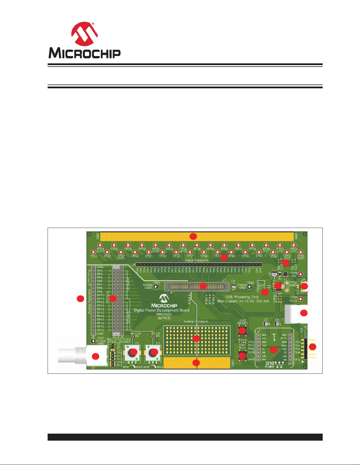
The Digital Power Development Board has the following features, as shown in Figure 1-1.
DIGITAL POWER DEVELOPMENT
BOARD USER’S GUIDE
Chapter 1. Overview
FIGURE 1-1: DIGITAL POWER DEVELOPMENT BOARD
1. Socket for DP PIM boards.
2. Digital GPIO test points. Pin header with connection to the digital test points.
3. ADC and DAC test points.
4. External analog signal input.
5. Potentiometer for DC level insertion from GND to +3.3V; it can be connected to
the lower half of the ADC inputs.
2018 Microchip Technology Inc. DS50002814A-page 9
Page 10

Digital Power Development Board User’s Guide
6. Potentiometer for DC level insertion from GND to +3.3V; it can be connected to
the upper half of the ADC inputs.
7. Analog input connection jumpers.
8. User push button.
9. Reset push button.
10. mikroBUS socket.
11. ICSP™ header to program the on-board MCU (6-pin, 2.54 mm header).
12. ICSP header to program the on-board MCU (RJ25 connector).
13. General purpose soldering pad area.
14. Solder pads for ground connection.
15. USB connector.
16. On-board LDO with Power Good (PG) function.
17. Power indicator LED (Green).
18. User LEDs (Red and Green).
Board dimensions are: 160 mm (length) x 100 mm (height).
1.2.1 Socket for DP PIM Boards
Insert the DP PIM board under test into the socket located in the middle of the Digital
Power Development Board. Socket J1 has a slot that defines the DP PIM board
direction. Be careful not to break the slot when inserting the DP PIM board into
the socket.
1.2.2 Test Points
The Digital Power Development Board ensures good signal integrity and provides
access to all pins of a DP PIM board. Each signal line is named after the DP PIM edge
connector pin number, with a “TP” (Test Point) prefix on the schematic diagram, which
is similarly marked on the silkscreen. These signals are divided into two main sections:
Analog and Digital (see Figure 1-1). For a detailed pinout, refer to the User’s Guide of
the DP PIM under test.
1. Analog Section
The analog section is located at the left connector side (smaller sector of the
socket). It consists of 18 signal lines, all referenced to analog ground. These lines
are split into two subsections:
•ADC inputs
• DAC output
2. Digital Section
The digital section is located at the right connector side (larger sector of the
socket). It consists of 31 lines, all referenced to digital ground. These lines
support all the digital lines of the DP PIMs. Some of them have dedicated
functions, such as:
• High-speed PWM outputs
• Medium speed GPIO
• Communication lines (SPI, I
• User push button and LEDs
2
C, UART)
DS50002814A-page 10 2018 Microchip Technology Inc.
Page 11

Overview
1.2.3 Grounding System
The entire board ground potential is connected together and forms one galvanically
common domain. The labels, “Analog” and “Digital”, indicate the geometrical domain.
The copper pour connected to the ground potential is split into two geometrical
domains, but the two geometrical domains are jointed together under the PIM socket,
thus improving the signal integrity and keeping noise confined to near their sources.
1.2.4 External Analog Signal Input
It is possible to insert an analog signal to any ADC input from a signal generator via a
standard BNC connector. The input impedance is 50. Input signals between the
ground and +3.3V are accepted. An overvoltage protection is implemented on this input
with a series resistor, and a pair of parallel diodes between the ground and the positive
supply rail.
1.2.5 DC Level Insertion
Two on-board potentiometers are connected between the ground and the +3.3V supply
rail to provide two stable DC levels. The two DC levels can be set independently with
potentiometers: P1 and P2. These DC signals can be used as an input signal to any
ADC input. The DC level set by P1 can be connected to the upper half, while P2 can
be connected to the lower half of the ADC inputs, at the analog input connection
jumpers.
1.2.6 Analog Input Connection Jumpers
The ADC inputs of the DP PIM board can be accessed directly from the pin header (J3)
located at the left side of the board. These inputs can also be connected to either the
external analog signal input (J7) or to the DC level insertion, respectively. The
three-row pin header matrix, J4, J5, J6 (No. 7 in Figure 1-1), forms a three-pin selection
jumper for each ADC input. When placing a jumper over the left, or over the right and
the middle pins, the corresponding ADC input can be connected to the extra input as
indicated on the silkscreen. The left side pins connect the external analog signal input,
while the right side pins connect the DC level insertion to the given ADC input. Two
positions on the DAC outputs are not connected. The pins on those positions are just
placeholders to keep the pin order. Three pins are connected to GND at both ends of
the jumper row. Jumpers can be stored on those pins if not needed. Two jumpers are
provided in the kit.
1.2.7 Push Buttons
There are two push buttons on the board: SW1 and SW2. Push button SW2, which is
directly connected to the RESET pin of the DP PIM board, is for the system Reset. For
dual core devices, this RESET is connected to the Master core Reset line. Push button
SW1 is a general purpose user interface connected to the TP27 test point and the
corresponding pin on the DP PIM.
1.2.8 MikroBUS™ Socket
A standard extension socket (J10) is provided on the board for mikroBUS
click boards™. The functionality of the board can be easily extended by using this
feature. The DP PIM board communicates with the mikroBUS socket via dedicated SPI
lines and the I
corresponding pins of the mikroBUS socket. The Reset button is connected to the
mikroBUS socket RESET pin.
2
C bus. Both +5V and +3.3V supply rails are connected to the
2018 Microchip Technology Inc. DS50002814A-page 11
Page 12

Digital Power Development Board User’s Guide
1.2.9 ICSP™ Programming Port
Dedicated lines for programming the MCU device on the inserted DP PIM board are
accessible via an RJ-25 modular connector or on a 6-pin header.
1.2.10 General Purpose Soldering Pad Area
The soldering point matrix on the bottom of the board with Plated-Through-Hole (PTH)
pads can be used to assemble any small extension circuitry needed for testing or
prototyping.
1.2.11 Solder Pad for Ground Connection
A bare gold-plated copper area is located on the upper and the bottom edges of the
board. These areas can either be used for soldering a solid ground connection or for
attaching alligator clips to connect instrument ground.
1.2.12 USB Connector
The Digital Power Development Board can be powered via the micro USB connector,
J2, at the right side of the board. The DP PIM board supply input and the +5V power
rail for the mikroBUS click board are directly connected to the positive supply line of the
USB. This connector is only for powering. The input voltage must be in the range of
3.6V to 6.3V. The mikroBUS click board can tighten this constraint; please refer to the
specifications before powering. Communication is not possible via this USB connector.
1.2.13 On-Board LDO
The +3.3V power rail for the mikroBUS click board is supplied by the on-board LDO
(Microchip’s MCP1755), connected to the +5V supply rail coming from the USB. The
total load for the mikroBUS click board supply current and the additional load caused
by its active GPIO lines should not exceed 300 mA. The DC level insertion
potentiometer and the pull-up resistor of the user push button are also connected to this
line. The Power Good output drives the Reset line of the board, ensuring stable
performance.
1.2.14 Power Indicator LED
The green LED (LD1) is on when the supply voltage is applied on the +5V supply rail.
1.2.15 User LEDs
The Digital Power Development Board has two user-programmable on-board LEDs.
The red LED is connected to TP52, while the green LED is connected to TP54. Logic
level high drives the LEDs.
1.3 ELECTRICAL CHARACTERISTICS
Ta bl e 1- 1 shows the electrical characteristics of the Digital Power Development Board.
TABLE 1-1: ELECTRICAL CHARACTERISTICS
Parameter Value
Input Voltage Range 3.6 VDC to 6.3 VDC
Current Consumption <10 mA
Maximal Load Current 1A
Operating Temperature Range 0°C to +65°C
DS50002814A-page 12 2018 Microchip Technology Inc.
Page 13

Appendix A. Board Layout and Schematics
A.1 PINOUT
DIGITAL POWER DEVELOPMENT
BOARD USER’S GUIDE
This appendix contains the pinout, schematics and board layouts for the Digital Power
Development Board. The topics covered in this appendix include:
• Pinout
• Board Schematic
• PCB Layout
Ta bl e A- 1 shows the pinout of the Digital Power Development Board.
TABLE A-1: PINOUT
Name Edge Connector Pin Default Function/Description
GND 1, 2 Analog Ground
DAC OUT 3, 7 DAC Output
ADC IN 4..6, 8..20 Analog Input
Slot 21..22 Aligning Slot
GPIO 23 Digital General Purpose
GPIO 24 Digital General Purpose and SPI_MISO
GPIO 25..31 Digital General Purpose
GPIO 32 Digital General Purpose and SPI_SCK
GPIO 33..35 Digital General Purpose
GPIO 36 Digital General Purpose and SPI_MOSI
GPIO 37..38 Digital General Purpose
GPIO 39 Digital General Purpose and
SER0 (UART to mikroBUS™ socket)
GPIO 40..44 Digital General Purpose
PWM1H 45 PWM Output
GPIO 46 Digital General Purpose
PWM1L 47 PWM Output
GPIO 48 Digital General Purpose and SPI Chip Select
MCLR
GPIO 50 Digital General Purpose and
PGEC 51 Programming/Debugging Line
GPIO 52 Digital General Purpose and Red LED
SCL 53 I2C Clock Line
GPIO 54 Digital General Purpose and Green LED
SDA 55 I2C Data Line
PGED 56 Programming/Debugging Line
5V 57, 59 V
GND 58, 60 Digital Ground
49 Reset
SER1 (UART to mikroBUS socket)
DD Rail
2018 Microchip Technology Inc. DS50002814A-page 13
Page 14

Designed with
Altium.com
+5V
5V 1A
TP64
GNDGND
GND
GND GND GND
100R
1206
1%
R13
100R
1206
1%
R14
GND
+5V
GND
+3.3V
GND
+3.3V
33 μF
10V
AL-B
C2
3.3 V
PEAK
Maximum
10 μF
16V
AL-A
C5
GND
+3.3V
MIN
MAX
1k
0603
1%
R8
GND
GNDGND
GNDGND
GND
MCLR
PGEC
PGED
3.3k
0603
1%
R3
GND
+3.3V
TP27_SW1
GNDGND
+3.3V
1 2 3 4 50
DNGV5+-D+DDI
Micro-AB Receptacle
USB2.0 MICRO-B FEMALE
J2
V
IN
2
SHDN
1
GND
3
PWRGD
5
V
OUT
4
EP
6
MCP1755/3.3V
U1
+5V
GND
+3.3V
GND GND
10 μF
16V
AL-A
C7
10 μF
16V
AL-A
C8
GND
MCLR_IN
GND GND
RST2CS3SCK4MISO5MOSI6+3.3V7GND
8
PWM
16
INT
15
RX
14
TX
13
SCL
12
SDA
11
+5V
10
GND
9
AN
1
mikroBUS™ HOST Socket
J10
RED
0603
LD2
1 4
2 3
TACT SPST
SW1
TP24_MISO
TP25 TP26
TP27_SW1 TP28
TP29 TP30
TP31 TP32_SCK
TP33 TP34
TP35 TP36_MOSI
TP37 TP38
TP39_SER0 TP40
TP41 TP42
TP43 TP44
TP45 TP46
TP47 TP48_CS
TP52_LD2
TP53_SCL TP54_LD3
TP55_SDA
TP50_SER1
TP53_SCL
TP55_SDA
Mikro_An
TP24_MISO
TP32_SCK
TP36_MOSI
TP48_CS
PGED
MCLR
PGEC
GREEN
0603
LD3
12345678910111213141516171819
20
HDR-2.54 Male 1x20
J3
TP3 TP4
TP5 TP6
TP7 TP8
GREEN
0603
LD1
TP9 TP10
TP11 TP12
TP13 TP14
TP15 TP16
TP17 TP18
TP19 TP20
1.5k
0603
1%
R5
3.3k
0603
1%
R4
1.5k
0603
1%
R2
0.01 μF
100V
0603
C4
1 2
3
4
5
6
7
8
9
10
11
12
13
14
15
16
17
18
19
20
23 24
25
26
27
28
29
30
31
32
33
34
35
36
37
38
39
40
41
42
43
44
45 46
47
48
49 50
51 52
53 54
55 56
57 58
59 60
EDGE 60P Female
J1
1 μF
50v
0603
C3
1 μF
50v
0603
C9
10 μF
16V
0805
C11
10 μF
16V
0805
C1
1R
1206
1%
R1
Shunt 2.54 mm 1x2 Handle
JP1
GND
TP3
TP4
TP5
TP6
TP7
TP8
TP9
TP10
TP11
TP12
TP13
TP14
TP15
TP16
TP17
TP18
TP19
TP20
12345678910111213141516171819
20
HDR-2.54 Male 1x20
J6
12345678910111213141516171819
20
HDR-2.54 Male 1x20
J5
12345678910111213141516171819
20
HDR-2.54 Male 1x20
J4
1N4148
D2
1N4148
D1
BNC_In P1_In
1
4
2
3
TACT SPST
SW2
User Switch
RESET
GND
TP65
Analog test points Input Signal Selection
Short with a jumper for P1/P2Short with a jumper for BNC
2
1 3
10k
P090S
20%
P1
TP24 TP26 TP28 TP30 TP32 TP34 TP36 TP38 TP40 TP42 TP44 TP46 TP48 TP52 TP54TP50TP25 TP27 TP29 TP31 TP33 TP35 TP37 TP39 TP41 TP43 TP45 TP47
TP60
GND
TP55TP53
TP25
TP27_SW1
TP29
TP31
TP33
TP35
TP37
TP39_SER0
TP41
TP43
TP45
TP47
TP53_SCL
TP55_SDA
TP24_MISO
TP26
TP28
TP30
TP32_SCK
TP34
TP36_MOSI
TP38
TP40
TP42
TP44
TP46
TP48_CS
TP52_LD2
TP54_LD3
TP50_SER1
Digital test points
1 μH
L3W3H1.5
NR3015T1R0N
L1
GND
TP4
TP5
TP6
TP8
TP9
TP10
TP11
TP12
TP13
TP14
TP15
TP16
TP17
TP18
TP19
TP20
12345
6
HDR-2.54 Male 1x6
J11
PGED
PGEC
GND
+3.3V
GND
TP23
TP23
TP23
MCLR
+3.3V
GND
150R
0603
1%
R7
MCLR_IN
0.01 μF
100V
0603
C6
22k
0603
1%
R6
MCLR_IN
1
2
3
4
5
6
1
MODULAR RJ25 R/A
J9
Shunt 2.54 mm 1x2 Handle
JP2
(TP3 is DAC Out)
(TP7 is DAC Out)
1
2
RF Coaxial BNC Female
J7
TP LOOP Black TH
TP62
GND
TP LOOP Black TH
TP63
GND
TP LOOP Black TH
TP61
GND
100R
1206
1%
R12
100R
1206
1%
R10
100R
1206
1%
R11
GND
+3.3V
MIN
MAX
1k
0603
1%
R9
GNDGND
1 μF
50v
0603
C10
P2_In
2
1 3
10k
P090S
20%
P2
Mikro_AnTP12
0R
0603
R15
1
2
3
4
5
6
7
8
9
10
11
12
13
14
15
16
17
18
19
20
21
22
23
24
25
26
27
28
29
30
31
32
33
34
35
36
HDR-2.54 Male 1x36
J8
TP23
TP24_MISO
TP25
TP26
TP27_SW1
TP29
TP31
TP33
TP35
TP37
TP39_SER0
TP41
TP43
TP45
TP47
TP53_SCL
TP55_SDA
TP28
TP30
TP32_SCK
TP34
TP36_MOSI
TP38
TP40
TP42
TP44
TP46
TP48_CS
TP52_LD2
TP54_LD3
TP50_SER1
GND GND
Mikro_PWM
0R
0603
R16
TP45
Mikro_PWM
Mikro_SER0
0R
0603
R17
Mikro_SER1
0R
0603
R18
TP39_SER0
TP50_SER1
Mikro_SER0
Mikro_SER1
SER0 and SER1 can be either a CAN
b
b
.
Digital Power Development Board User’s Guide
Figure A-1 shows the board schematic.
FIGURE A-1: DIGITAL POWER DEVELOPMENT BOARD SCHEMATIC
A.2 BOARD SCHEMATIC
DS50002814A-page 14 2018 Microchip Technology Inc.
us or a UART port between the DP PIM
oard and the mikroBUS
Page 15
Board Layout and Schematics
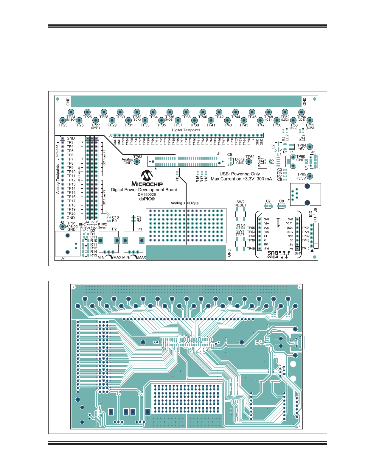
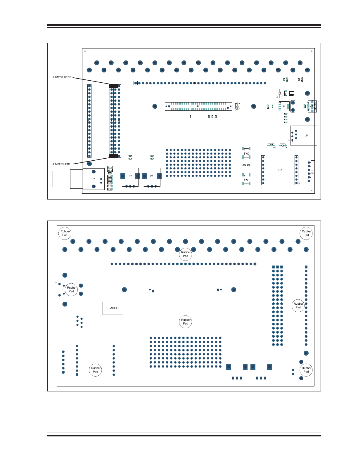
A.3 PCB LAYOUT
The Digital Power Development Board is a two-layer FR4, 1.55 mm,
Plated-Through-Hole PCB construction. Figure A-2 through Figure A-5 illustrate the
PCB layers. Figure A-6 and Figure A-7 show the assembly drawings of the Digital
Power Development Board.
FIGURE A-2: DIGITAL POWER DEVELOPMENT BOARD TOP SILKSCREEN
FIGURE A-3: DIGITAL POWER DEVELOPMENT BOARD TOP COPPER
2018 Microchip Technology Inc. DS50002814A-page 15
Page 16
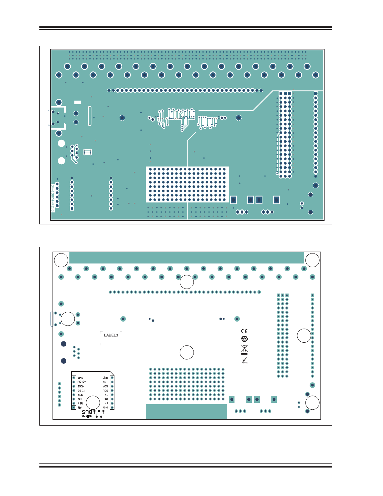
Digital Power Development Board User’s Guide
FIGURE A-4: DIGITAL POWER DEVELOPMENT BOARD BOTTOM COPPER (BOTTOM VIEW)
FIGURE A-5: DIGITAL POWER DEVELOPMENT BOARD BOTTOM SILKSCREEN
(BOTTOM VIEW)
DS50002814A-page 16 2018 Microchip Technology Inc.
Page 17
Board Layout and Schematics
3
2
7
0
11 15 19 23 27 31 35
0
0
19
15
11
7
3
1
19 19
15 15
11 11
7 7
3 3
000000
00
00000 0
0 0
0 00 0
0 00 0
0 00
0 00
3
7
4
4
2
1
20
1818
16
17
12
13
9
10
5
6
2
4
1
1 1
20
1818201818
161716
17
121312
13
9109
10
565
6
242
4
1 1
1
1 2
MH
1 2
31
1
65
00
00
00
00
00
98
1
00
00
00
00
0 0
1312
1
00
00
00
00
0 0
1614
0 0
0 0
0 0
0 0
00
1817
0 00 0
0 00 0
0 00 0
0 00 0
00 00
2221
0 00
0 00
0 00
0 00
0 00
2524
1
0
2928
1
3230
1
3433
1
4
2
6
5
1
2
3
5
6
1
1
2
3
6
5
1
1
1
2
14
8
2
14 14
8 8
1 1 1
00 00 00 0 010 00 010 00
1 1
8
1
1
19
15
11
7
3
0 000
0 000
00 00
00 00
0
14
10
3
MH MH
20
1818
16
17
12
13
9
10
5
6
2
4
4
1
1 1
0 000
MH
0 000
0 000
0 000
0 000
0
10
1
00 00
00 00
00 00
00 00
0000
2620
1
16
15
13
12
11
1
36
11
0
1
14
8
1
0 000
1 1
00 00
1 1
9
1
0
1
1
2
2
2
1
122
1
2
1
2
2
1
1
2
1
2
5
4
1
1
2
1
56910111215
16
1
2
25262728313237
38
2
1
4142434447485354575859
60
2
1
1
2
1
3
1
3
1
3
2
224
4
1
21
2 1
2 1
1
2
2 1
1
1
2
2
4
2
1
2 2
2
1
2
2
2
1
2
12347813141718192023242930333435
36
121
2
394045464950515255
56
21
3
5
2
1
1
2
1
2
1
1 1
1
0
0
0
0
6
FIGURE A-6: DIGITAL POWER DEVELOPMENT BOARD TOP ASSEMBLY
FIGURE A-7: DIGITAL POWER DEVELOPMENT BOARD BOTTOM ASSEMBLY
(BOTTOM VIEW)
1
1
1
1
1
0
0
0
0
1
6
4
2
6
5
4
3
2
1
8
7
6
5
4
3
2
1
2018 Microchip Technology Inc. DS50002814A-page 17
1
1
5
3
1
1 1
11
1
32 30
34 33
36
1
9
10
11
12
13
14
15
16
1
29 28
11
1
25 24
26 20
0
0
0 00 0
00 0
00 00
00 0
00 0
00 0
00 0
00 0
00 0
22 21
00 00
00 00
00 00
00 00
00 00
1
18 17
0 0
0000
0000
0000
0000
0000
0000
0000
1
16 14
00
0 0
00
0 0
0 0
00
0 0
00
0 0
00
0 0
000000 00
000 0
1
11151923273135
13 12
00
0 0
0 0
0 0
0 0
0 0
0 0
11
1
3
7
6 5
9 8
10
0
0
00
00
000 0
000 00 000100 00100 0
000 0
00
000 0
00
000 0
00
000 0
00
000 0
00
000 0
MH
1
2
3 1
4
111
1
11
12
MH
3
11
242
33
4
565
6
77
88
9109
10
1111
121312
13
1414
1515
161716
17
1818201818
1919
20
MHMH
12
1
1
1
2
3
4
5
6
7
8
9
10
11
12
13
14
15
16
17
1818
19
20
2
1
2
2
11
1
2
3
4
5
6
7
8
9
10
11
12
13
14
15
16
17
1818
19
20
1
Page 18

Digital Power Development Board User’s Guide
NOTES:
DS50002814A-page 18 2018 Microchip Technology Inc.
Page 19

DIGITAL POWER DEVELOPMENT
BOARD USER’S GUIDE
Appendix B. Bill of Materials (BOM)
This appendix contains the Bill of Materials (BOM) for the Digital Power Development
Board.
• Bill of Materials
B.1 BILL OF MATERIALS
Ta bl e B -1 shows the Bill of Materials for the Digital Power Development Board.
TABLE B-1: DIGITAL POWER DEV. BOARD BILL OF MATERIALS (BOM)
Qty. Designator Description Manufacturer Manufacturer Part Number
2 C1, C11 Capacitor, Ceramic, 10 µF, 16V,
20%, X7R, SMD, 0805
1 C2 Capacitor Aluminum, 33 µF,
10V, 20%, SMD, B
3 C3, C9, C10 Capacitor Ceramic, 1 µF, 50V,
10%, X7R, SMD, 0603
2 C4, C6 Capacitor Ceramic, 0.01 µF,
100V, 10%, X7R, SMD, 0603
3 C5, C7, C8 Capacitor, Aluminum, 10 µF,
16V, 20%, SMD, A
2 D1, D2 Diode, Rectifier, 1N4148,
855 mV, 300 mA, 75V, SOD-323
1 J1 Connector, Edge, MECF,
1.27 mm, 60P, Female, SMD,
Verti cal
1 J2 Connector, USB 2.0, micro-B,
Female, TH/SMD, R/A
4 J3, J4, J5, J6 Connector Header-2.54, Male,
1x20, Gold, 5.84 MH, TH,
Verti cal
1 J7 Connector, RF, Coaxial, BNC,
Female, 2P, TH, RA
1 J8 Connector Header-2.54, Male,
1x36, Gold, 5.84 MH, TH
1 J9 Connector, Modular, RJ25, TH,
R/A
2 J10 Socket, mikroBUS™, Host, DIP,
16, TH
1 J11 Connector Header-2.54, Male,
1x6, Gold, 5.84 MH, TH, R/A
1 L1 Inductor, 1 µH, 2.1A, 30%, SMD,
L3W3H1.5
1 LD1 Diode, LED, Green, 2V, 30 mA,
35 mcd, Clear, SMD, 0603
Taiyo Yuden Co., Ltd. EMK212BB7106MG-T
®
Panasonic
Taiyo Yuden Co., Ltd. UMK107AB7105KA-T
TDK Corporation C1608X7R2A103K080AA
Nichicon Corporation UWX1C100MCL2GB
Diodes Incorporated
Samtec, Inc. MECF-30-01-L-DV-WT
FCI 10118194-0001LF
Samtec, Inc. TSW-120-07-G-S
Amphenol Commercial 31-5431-2010
Sullins Connector
Solutions
Tyco Electronics (TE
Connectivity Ltd.)
Sullins Connector
Solutions
FCI 68016-106HLF
Taiyo Yuden Co., Ltd. NR3015T1R0N
Lite-On
- ECG EEE-1AA330WR
®
1N4148WS-7-F
PBC36SAAN
5555165-1
PPTC081LFBN-RC
®
, Inc. LTST-C190KGKT
2018 Microchip Technology Inc. DS50002814A-page 19
Page 20
Digital Power Development Board User’s Guide
TABLE B-1: DIGITAL POWER DEV. BOARD BILL OF MATERIALS (BOM) (CONTINUED)
Qty. Designator Description Manufacturer Manufacturer Part Number
1 LD2 Diode, LED, Red, 1.8V, 40 mA,
10 mcd, Clear, SMD, 0603
1 LD3 Diode, LED, Green, 2.2V, 25 mA,
18 mcd, Diffuse, SMD, 0603
2 P1, P2 Resistor, Variable, 10K, 20%,
TH, P090S
1 R1 Resistor, TKF, 1R, 1%, 1/2W,
SMD, 1206
1 R2 Resistor, TKF, 1.5k, 1%, 1/10W,
SMD, 0603
3 R3, R4, R5 Resistor, TKF, 3.3k, 1%, 1/10W,
SMD, 0603
1 R6 Resistor, TKF, 22k, 1%, 1/10W,
SMD, 0603
1 R7 Resistor, TKF, 150R, 1%,
1/10W, SMD, 0603
2 R8, R9 Resistor, TKF, 1k, 1%, 1/10W,
SMD, 0603
5 R10, R11, R12,
R13, R14
4 R15, R16, R17,
R18
2 SW1, SW2 Switch, Tact, SPST, 12V, 50 mA,
31 TP23, TP24,
TP25, TP26,
TP27, TP28,
TP29, TP30,
TP31, TP32,
TP33, TP34,
TP35, TP36,
TP37, TP38,
TP39, TP40,
TP41, TP42,
TP43, TP44,
TP45, TP46,
TP47, TP48,
TP50, TP52,
TP53, TP54,
TP55
1 TP60 Connector, TP, Tab, 0.250, TH Tyco Electronics (TE
3 TP61, TP62,
TP63
2 TP64, TP65 Connector, TP, Loop, Red, TH Keystone Electronics
1 U1 Microchip Analog, LDO, 3.3V,
Resistor, TKF, 100R, 1%, 1/4W,
SMD, 1206
Resistor, TKF, 0R, 1/10W, SMD,
0603
MCLTL-613R
Connector, TP, Loop, Orange, THKeystone Electronics
Connector, TP, Loop, Black, TH Keystone Electronics
MCP1755T-3302E/DC,
SOT-223-5
Lite-On®, Inc. LTST-C190KRKT
®
Lumex
TT Electronics Plc. P090S-14T20BR10K
Stackpole Electronics,
Inc.
Panasonic
Panasonic - ECG ERJ-3EKF3301V
Panasonic - ECG ERJ-3EKF2202V
Stackpole Electronics,
Inc.
Panasonic - ECG ERJ-3EKF1001V
Yageo Corporation RC1206FR-07100RL
NIC Components Corp. NRC06Z0TRF
Multicomp Inc. MCLTL-613R
Corp.
Connectivity Ltd.)
Corp.
Corp.
Microchip Technology
Inc.
Inc. SML-LX0603GW-TR
CSR1206FT1R00
®
- ECG ERJ-3EKF1501V
RMCF0603FT150R
5013
1217861-1
5011
5010
MCP1755T-3302E/DC
DS50002814A-page 20 2018 Microchip Technology Inc.
Page 21

NOTES:
Bill of Materials (BOM)
2018 Microchip Technology Inc. DS50002814A-page 21
Page 22

Worldwide Sales and Service
AMERICAS
Corporate Office
2355 West Chandler Blvd.
Chandler, AZ 85224-6199
Tel: 480-792-7200
Fax: 480-792-7277
Technical Support:
http://www.microchip.com/
support
Web Address:
www.microchip.com
Atlanta
Duluth, GA
Tel: 678-957-9614
Fax: 678-957-1455
Austin, TX
Tel: 512-257-3370
Boston
Westborough, MA
Tel: 774-760-0087
Fax: 774-760-0088
Chicago
Itasca, IL
Tel: 630-285-0071
Fax: 630-285-0075
Dallas
Addison, TX
Tel: 972-818-7423
Fax: 972-818-2924
Detroit
Novi, MI
Tel: 248-848-4000
Houston, TX
Tel: 281-894-5983
Indianapolis
Noblesville, IN
Tel: 317-773-8323
Fax: 317-773-5453
Tel: 317-536-2380
Los Angeles
Mission Viejo, CA
Tel: 949-462-9523
Fax: 949-462-9608
Tel: 951-273-7800
Raleigh, NC
Tel: 919-844-7510
New York, NY
Tel: 631-435-6000
San Jose, CA
Tel: 408-735-9110
Tel: 408-436-4270
Canada - Toronto
Tel: 905-695-1980
Fax: 905-695-2078
ASIA/PACIFIC
Australia - Sydney
Tel: 61-2-9868-6733
China - Beijing
Tel: 86-10-8569-7000
China - Chengdu
Tel: 86-28-8665-5511
China - Chongqing
Tel: 86-23-8980-9588
China - Dongguan
Tel: 86-769-8702-9880
China - Guangzhou
Tel: 86-20-8755-8029
China - Hangzhou
Tel: 86-571-8792-8115
China - Hong Kong SAR
Tel: 852-2943-5100
China - Nanjing
Tel: 86-25-8473-2460
China - Qingdao
Tel: 86-532-8502-7355
China - Shanghai
Tel: 86-21-3326-8000
China - Shenyang
Tel: 86-24-2334-2829
China - Shenzhen
Tel: 86-755-8864-2200
China - Suzhou
Tel: 86-186-6233-1526
China - Wuhan
Tel: 86-27-5980-5300
China - Xian
Tel: 86-29-8833-7252
China - Xiamen
Tel: 86-592-2388138
China - Zhuhai
Tel: 86-756-3210040
ASIA/PACIFIC
India - Bangalore
Tel: 91-80-3090-4444
India - New Delhi
Tel: 91-11-4160-8631
India - Pune
Tel: 91-20-4121-0141
Japan - Osaka
Tel: 81-6-6152-7160
Japan - Tokyo
Tel: 81-3-6880- 3770
Korea - Daegu
Tel: 82-53-744-4301
Korea - Seoul
Tel: 82-2-554-7200
Malaysia - Kuala Lumpur
Tel: 60-3-7651-7906
Malaysia - Penang
Tel: 60-4-227-8870
Philippines - Manila
Tel: 63-2-634-9065
Singapore
Tel: 65-6334-8870
Taiwan - Hsin Chu
Tel: 886-3-577-8366
Taiwan - Kaohsiung
Tel: 886-7-213-7830
Taiwan - Taipei
Tel: 886-2-2508-8600
Thailand - Bangkok
Tel: 66-2-694-1351
Vietnam - Ho Chi Minh
Tel: 84-28-5448-2100
EUROPE
Austria - Wels
Tel: 43-7242-2244-39
Fax: 43-7242-2244-393
Denmark - Copenhagen
Tel: 45-4450-2828
Fax: 45-4485-2829
Finland - Espoo
Tel: 358-9-4520-820
France - Paris
Tel: 33-1-69-53-63-20
Fax: 33-1-69-30-90-79
Germany - Garching
Tel: 49-8931-9700
Germany - Haan
Tel: 49-2129-3766400
Germany - Heilbronn
Tel: 49-7131-67-3636
Germany - Karlsruhe
Tel: 49-721-625370
Germany - Munich
Tel: 49-89-627-144-0
Fax: 49-89-627-144-44
Germany - Rosenheim
Tel: 49-8031-354-560
Israel - Ra’anana
Tel: 972-9-744-7705
Italy - Milan
Tel: 39-0331-742611
Fax: 39-0331-466781
Italy - Padova
Tel: 39-049-7625286
Netherlands - Drunen
Tel: 31-416-690399
Fax: 31-416-690340
Norway - Trondheim
Tel: 47-7288-4388
Poland - Warsaw
Tel: 48-22-3325737
Romania - Bucharest
Tel: 40-21-407-87-50
Spain - Madrid
Tel: 34-91-708-08-90
Fax: 34-91-708-08-91
Sweden - Gothenberg
Tel: 46-31-704-60-40
Sweden - Stockholm
Tel: 46-8-5090-4654
UK - Wokingham
Tel: 44-118-921-5800
Fax: 44-118-921-5820
DS50002814A-page 22 2018 Microchip Technology Inc.
08/15/18
 Loading...