

Page 1
CAN/LIN/J2602 PICtail™ (Plus)
Daughter Board User’s Guide
2011 Microchip Technology Inc. DS70319B
Page 2

Note the following details of the code protection feature on Microchip devices:
• Microchip products meet the specification contained in their particular Microchip Data Sheet.
• Microchip believes that its family of products is one of the most secure families of its kind on the market today, when used in the
intended manner and under normal conditions.
• There are dishonest and possibly illegal methods used to breach the code protection feature. All of these methods, to our
knowledge, require using the Microchip products in a manner outside the operating specifications contained in Microchip’s Data
Sheets. Most likely, the person doing so is engaged in theft of intellectual property.
• Microchip is willing to work with the customer who is concerned about the integrity of their code.
• Neither Microchip nor any other semiconductor manufacturer can guarantee the security of their code. Code protection does not
mean that we are guaranteeing the product as “unbreakable.”
Code protection is constantly evolving. We at Microchip are committed to continuously improving the code protection features of our
products. Attempts to break Microchip’s code protection feature may be a violation of the Digital Millennium Copyright Act. If such acts
allow unauthorized access to your software or other copyrighted work, you may have a right to sue for relief under that Act.
Information contained in this publication regarding device
applications and t he lik e is provided only for your convenience
and may be su perseded by upda t es . It is y our responsibility to
ensure that your application meets with your specifications.
MICROCHIP MAKES NO REPRESENTATIONS OR
WARRANTIES OF ANY KIND WHETHER EXPRESS OR
IMPLIED, WRITTEN OR ORAL, STATUTORY OR
OTHERWISE, RELATED TO THE INFORMATION,
INCLUDING BUT NOT LIMITED TO ITS CONDITION,
QUALITY, PERFORMANCE, MERCHANTABILITY OR
FITNESS FOR PURPOSE. Microchip disclaims all liability
arising from this information and its use. Use of Microchip
devices in life supp ort and/or safety ap plications is entir ely at
the buyer’s risk, and the buyer agrees to defend, indemnify and
hold harmless M icrochip from any and all dama ges, claims,
suits, or expenses re sulting from such use. No licens es are
conveyed, implicitly or otherwise, under any Microchip
intellectual property rights.
Trademarks
The Microchip name and logo, the Microchip logo, dsPIC,
K
EELOQ, KEELOQ logo, MPLAB, PIC, PICmicro, PICSTART,
32
PIC
logo, rfPIC and UNI/O are registered trademarks of
Microchip Technology Incorporated in the U.S.A. and other
countries.
FilterLab, Hampshire, HI-TECH C, Linear Active Thermistor,
MXDEV, MXLAB, SEEVAL and The Embedded Control
Solutions Company are registered trademarks of Microchip
Technology Incorporated in the U.S.A.
Analog-for-the-Digital Age, Application Maestro, CodeGuard,
dsPICDEM, dsPICDEM.net, dsPICworks, dsSPEAK, ECAN,
ECONOMONITOR, FanSense, HI-TIDE, In-Circuit Serial
Programming, ICSP, Mindi, MiWi, MPASM, MPLAB Certified
logo, MPLIB, MPLINK, mTouch, Omniscient Code
Generation, PICC, PICC-18, PICDEM, PICDEM.net, PICkit,
PICtail, REAL ICE, rfLAB, Select Mode, Total Endurance,
TSHARC, UniWinDriver, WiperLock and ZENA are
trademarks of Microchip Technology Incorporated in the
U.S.A. and other countries.
SQTP is a service mark of Microchip Technology Incorporated
in the U.S.A.
All other trademarks mentioned herein are property of their
respective companies.
© 2011, Microchip Technology Incorporated, Printed in the
U.S.A., All Rights Reserved.
Printed on recycled paper.
ISBN: 978-1-60932-934-1
Microchip received ISO/TS-16949:2002 certification for its worldwide
headquarters, design and wafer fabrication facilities in Chandler and
Tempe, Arizona; Gresham, Oregon and design centers in California
and India. The Company’s quality system processes and procedures
are for its PIC
devices, Serial EEPROMs, microperipherals, nonvolatile memory and
analog products. In addition, Microchip’s quality system for the design
and manufacture of development systems is ISO 9001:2000 certified.
®
MCUs and dsPIC® DSCs, KEELOQ
®
code hopping
DS70319B-page 2 2011 Microchip Technology Inc.
Page 3

CAN/LIN/J2602 PICtail™ (Plus)
DAUGHTER BOARD USER’S GUIDE
Table of Contents
Preface ...........................................................................................................................5
Chapter 1. Introduction
1.1 Overview ............. ......................................................................................... 11
1.2 Functional Overview .....................................................................................13
Chapter 2. Hardware
2.1 Board Setu p ............. .......................... .. .. ..................................................... . 15
2.2 Hardware Components ................................................................................16
2.3 Auxiliary Header Pinouts ..............................................................................19
Chapter 3. CAN/LIN/J2602 PICtail (Plus) Daughter Board Tutorial Program
3.1 PIC18 Tutorial Overview .............................................................................. 21
3.2 dsPIC33F and PIC24H Tutorial Overview ................. .................... ...............22
Appendix A. Drawings and Schematics
A.1 CAN/LIN/J2602 PICtail™ (Plus) Daughter Board Layou t .................. ..........23
A.2 Schematic Diagrams ............... ..................................................................... 24
Index .............................................................................................................................31
Worldwide Sales and Service ....................................................................................32
2011 Microchip Technology Inc. DS70319B-page 3
Page 4

CAN/LIN/J2602 PICtail™ (Plus) Daughter Board User’s Guide
NOTES:
DS70319B-page 4 2011 Microchip Technology Inc.
Page 5
CAN/LIN/J2602 PICtail™ (Plus)
DAUGHTER BOARD USER’S GUIDE
Preface
NOTICE TO CUSTOMERS
All documentation becomes dated, and this manual is no exception. Microchip tools and
documentation are constantly evolving to meet customer needs, so some actual dialogs
and/or tool descriptions may differ from those in this document. Please refer to our web site
(www.microchip.com) to obtain the latest documentation available.
Documents are identified with a “DS” number. This number is located on the bottom of each
page, in front of the p age number. The numbering convention for the DS number is
“DSXXXXXA”, where “XXXXX” is the document number and “A” is the revision level of the
document.
For the most up-to-date information on development tools, see the MPLAB
Select the Help menu, and then Topics to open a list of available online help files.
®
IDE on-line help.
INTRODUCTION
This chapter contains general information that will be useful to know before using the
CAN/LIN/J2602 PICtail
include:
• Document Layout
• Conventions Used in this Guide
• Warranty Registration
• Recommended Reading
• The Microchip Web Site
• Development Systems Customer Change Notification Service
• Customer Support
• Document Revision History
DOCUMENT LAYOUT
This document describes how to use the CAN/LIN/J2602 PICtail™ (Plus) Daughter
Board as a development tool to emulate and debug firmware on a target board. The
manual layout is as follows:
• Chapter 1. Introduction – This chapter introduces the CAN/LIN/J2602 PICtail
(Plus) Daughter Board and provides an overview of its features.
• Chapter 2. Hardwar e – This chapter provides a functional overview of the
CAN/LIN/J2602 PICtail (Plus) Daughter Board and identifies the major hardware
components.
• Appendix A. Drawings and Schematics – This appendix provides detailed
technical drawings and schematic diagrams of the CAN/LIN/J2602 PICtail (Plus)
Daughter Board.
™
(Plus) Daughter Board. Items discussed in this chapter
2011 Microchip Technology Inc. DS70319B-page 5
Page 6
CAN/LIN/J2602 PICtail™ (Plus) Daughter Board User’s Guide
CONVENTIONS USED IN THIS GUIDE
This manual uses the following docum entat io n conven tion s:
DOCUMENTATION CONVENTIONS
Description Represents Examples
Arial font:
Italic chara c ters Referenced books MPLAB
Emphasized text ...is the only compiler...
Initial caps A window the Output window
A dialog the Settings dialog
A menu selection select Enable Programmer
Quotes A field name in a window or
dialog
Underlined, italic text with
right angle bracket
Bold characters A dialog button Click OK
N‘Rnnnn A number in verilog format,
Text in angle brac kets < > A key on the keyboard Press <Enter>, <F1>
Courier New font:
Plain Courier New Sample source code #define START
Italic Courier New A variable argument file.o, where file can be
Square brackets [ ] Optional arguments mcc18 [options] file
Curly brackets and pipe
character: { | }
Ellipses... Replaces r epeated text var_name [,
A menu path File>Save
A tab Click the Power tab
where N is the tota l number of
digits, R is th e radi x and n is a
digit.
Filenames autoexec.bat
File paths c:\mcc18\h
Keywords _asm, _endasm, static
Command-line options -Opa+, -Opa-
Bit values 0, 1
Constants 0xFF, ‘A’
Choice of mut ually exclus ive
arguments; an OR selection
Represents code supplied by
user
“Save project before build”
4‘b0010, 2‘hF1
any valid filename
[options]
errorlevel {0|1}
var_name...]
void main (void)
{ ...
}
®
IDE User’s Guide
DS70319B-page 6 2011 Microchip Technology Inc.
Page 7

WARRANTY REGISTRATION
Please complete the enclosed Warranty Registration Card and mail it promptly.
Sending in the Warranty Registration Card entitles users to receive new product
updates. Interim software releases are available at the Microchip web site.
RECOMMENDED READING
This user’s guide describes how to use CAN/LIN/J2602 PICtail (Plus) Daughter Board.
Other useful documents are listed below. Microchip documents are available and
recommended as supplemental r eference resources.
Device Data Sh eets
Refer to the data sheet for the specific dsPIC33F or PIC24 device you are using.
Specifically , refer to the sections in these data sheets that provide detailed information
on the device UART and ECAN modules.
Readme Files
For the latest information on using other tools, read the tool-specific Readme files in
the Readmes subdirectory of the MPLAB
contain update information and known issues that may not be included in this user’s
guide.
Preface
®
IDE installation directory. The Readme files
THE MICROCHIP WEB SITE
Microchip provides online support via our web site at www.microchip.com. This web
site is used as a means to make files and information easily available to customers.
Accessible by using your favorite Internet browser, the web site contains the following
information:
• Product Support – Data sheets and errata, application notes and sample
programs, design resources, user’s guides and hardware support documents,
latest software releases and archived software
• General Technical Support – Frequently Asked Questions (FAQs), technical
support requests, online discussion groups, Microchip consultant program
member listing
• Business of Microchip – Product selector and ordering guides, latest Microchip
press releases, listing of seminars and events, listings of Microchip sales offices,
distributors and factory representatives
2011 Microchip Technology Inc. DS70319 B-page 7
Page 8

CAN/LIN/J2602 PICtail™ (Plus) Daughter Board User’s Guide
DEVELOPMENT SYSTEMS CUSTOMER CHANGE NOTIFICATION SERVICE
Microchip’s customer notification service helps keep customers current on Microchip
products. Subscribers will receive e-mail notification whenever there are changes,
updates, revisions or errata related to a specified product family or development tool of
interest.
To register, access the Microchip web site at www.microchip.com, click on Customer
Change Notification and follow the registration instructions.
The Development Systems product group categories are:
• Compilers – The latest information on Microchip C compilers and other language
tools. These include the MPLAB C18 and MPLAB C30 C compilers; MPASM™
and MPLAB ASM30 assemblers; MPLINK™ and MPLAB LINK30 object linkers;
and MPLIB™ and MPLAB LIB30 object librarians.
• Emulators – The latest information on Microchip in-circuit emulators.This
includes the MPLAB ICE 2000 and MPLAB ICE 4000.
• In-Circuit Debuggers – The latest information on the Microchip in-circuit
debugger, MPLAB ICD 2.
• MPLAB
Integrated Development Environment for development systems tools. This list is
focused on the MPLAB IDE, MPLAB SIM simulator, MPLAB IDE Project Manager
and general editing and debugging features.
• Programmers – The latest information on Microchip programmers. These include
the MPLAB PM3 and PRO MATE
Plus and PICkit™ 1 development programmers.
®
IDE – The latest information on Microchip MPLAB IDE, the Windows®
®
II device programmers and the PICSTART®
DS70319B-page 8 2011 Microchip Technology Inc.
Page 9

CUSTOMER SUPPORT
Users of Microchip products can receive assistance through several channels:
• Distributor or Representative
• Local Sales Office
• Field Application Engineer (FAE)
• Technical Support
Customers should contact their distributor, representative or field application engineer
(FAE) for support. Local sales offices are also available to help customers. A listing of
sales offices and locations is included in the back of this document.
Technical support is available through the web site at: http://support.microchip.com
Preface
2011 Microchip Technology Inc. DS70319 B-page 9
Page 10

CAN/LIN/J2602 PICtail™ (Plus) Daughter Board User’s Guide
DOCUMENT REVISION HISTORY
Revision A (January 2008)
• Initial Release of this Document.
Revision B (March 201 1)
• Added support for PIC18 Explorer Development Board.
DS70319B-page 10 2011 Microchip Technology Inc.
Page 11

Thank you for purchasing Microchip Technology’s CAN/LIN/J2602 PICtail™ (Plus)
Daughter Board. This board is compatible with both the Explorer 16 Development
Board and the PIC18 Explorer Board to facilitate rapid implementation and evaluation
of applications that use Controller Area Network (CAN) and Local Interconnect Network
(LIN) interfaces and are implemented on dsPIC33F Digital Signal Controllers, PIC24
16-bit microcontrollers and PIC18 8-bit microcontrollers.
This chapter introduces the CAN/LIN/J2602 PICtail™ (Plus) Daughter Board and
provides an overview of its features. Topics covered include:
• Overview
• Functional Overview
1.1 OVERVIEW
The CAN/LIN/J2602 PICtail™ (Plus) Daughter Board augments development of
dsPIC33F and PIC24 based applications on the Explorer 16 Development Board and
augments development of PIC18 based applications on the PIC18 Explorer Development Board. It offers two interfaces: one for a CAN bus and one for a LIN bus. Although
CAN and LIN protocols are used most extensively in automotive applications, the
CAN/LIN/J2602 PICtail™ (Plus) Daughter Board can be used in any application that
requires interfacing to a CAN and LIN bus.
Both interfaces can be used simultaneously. Appropriate bus transceivers on the
CAN/LIN/J2602 PICtail™ (Plus) Daughter Board complete the physical layer requirements of the CAN and LIN bus protocols. In both cases, communication is driven by
the dsPIC33F, PIC24 or PIC18 device on its respective development board.
Figure 1-1 shows the CAN/LIN/J2602 PICtail™ (Plus) Daughter Board plugged into the
PICtail Plus slot on the Explorer 16 Development Board, and Figure 1-2 shows the
CAN/LIN/J2602 PICtail™ (Plus) Daughter Board plugged into the PICtail slot on the
PIC18 Explorer Development Board. The CAN/LIN/J2602 PICtail™ (Plus) Daughter
Board draws 9V, 5V and 3.3V DC power from the connected development board. The
external power supply and MPLAB ICD 3 are plugged into the development board.
CAN/LIN/J2602 PICtail™ (Plus)
DAUGHTER BOARD USER’S GUIDE
Chapter 1. Introduction
2011 Microchip Technology Inc. DS70319B-page 11
Page 12
CAN/LIN/J2602 PICtail™ (Plus) Daughter Board User’s Guide
CAN/LIN/J2602 PICtail™ (Plus)
Daughter Board
Explorer 16 Development
Board
dsPIC33F or PIC24
Plug In Module
CAN/LIN/J2602 PICt ai l™ (Plus)
Daughter Board
PIC18 Explorer
Development Board
PIC18 Plug In
Module
FIGURE 1-1: CAN/LIN/J2602 PICtail™ (Plus) DAUGHTER BOARD
CONNECTED TO EXPLORER 16 DEVELOPMENT BOARD
FIGURE 1-2: CAN/LIN/J2602 PICtail
™
(Plus) DAUGHTER BOARD
CONNECTED TO PIC18 EXPLORER DEVELOPMENT BOARD
DS70319B-page 12 2011 Microchip Technology Inc.
Page 13

1.2 FUNCTIONAL OVERVIEW
LIN1
LIN2
CAN1
CAN2
LIN1
Transceiver
(U1)
LIN2
Transceiver
(U2)
CAN1
Transceiver
(U3)
CAN2
Transceiver
(U4)
CAN/LIN/J2602 PICtail™ (Plus) DAUGHTER BOARD DEVELOPMENT BOARD
Interrupt/Wake
Transmit Enab le
Receive
Transmit
Receive
High
Low
Transmit
Receive
High
Low
To UART Module on
dsPIC33F, PIC24 or PIC18
To ECAN Module on
dsPIC33F, PIC24 or PIC18
Bus
Bus
Bus
Bus
Transmit
Interrupt/Wake
Transmit Enab le
Receive
Transmit
The block diagram shown in Figure 1-3 illustrates the mainstream operation of the
CAN/LIN/J2602 PICtail™ (Plus) Daughter Board. The board contains two LIN signal
conditioning circuits and two CAN signal conditioning circuits. The board also enables
power to be provided by the development board it is connected to, or by an external
12V DC source.
Introduction
FIGURE 1-3: CAN/LIN/J2602 PICtail
™
(Plus) DAUGHTER BOARD BLOCK DIAGRAM
1.2.1 LIN Operation
2011 Microchip Technology Inc. DS70319B-page 13
The CAN/LIN/J2602 PICtail™ (Plus) Daughter Board connects two LIN transceivers
with integrated voltage regulators to UART modules on a dsPIC33F, PIC24 or PIC18
control device on the Explorer 16 or PIC18 Explorer Board. The LIN transceiver monitors the LIN bus, conditions the incoming signal and passes it to the UART module on
the control device. The LIN transceiver responds to a “Transmit Enable” from the control device by conditioning an output signal and placing it on the LIN bus.
A Power-down mode turns the transmitter and voltage regulator off, leaving only the
receiver and wake-up circuits in operation. Each LIN circuit includes a Master/Slave
jumper to accommodate a Master node on the LIN bus.
In order to use the transmit enable for the LIN2 transceiver with the PIC18 Explorer
Board and a PIC18 device, the LIN2TXE pin must be connected to 5V, or a pin on the
PIC18 device, to control it. This can be done by connecting a jumper wire on the J18
header between LIN2TXE and either the 5V supply also on the J18 header, or an available pin on either the J17 or J18 header. For more information on the J17 and J18
headers see Section 2.3 “Auxiliary Header Pinouts”.
Page 14

CAN/LIN/J2602 PICtail™ (Plus) Daughter Board User’s Guide
For PIC18 devices, the pinout for the LIN1 and LIN2 modules can be different. The
jumpers J4, J8, J13 and J14 are for choosing between these pinouts. For the specific
pinout that is necessary for the PIC18 that is used, refer to that device’s data sheet. For
PIC24 and dsPIC33 devices, make sure to leave the J4, J8, J13 and J14 jumpers
disconnected. Otherwise, these connections can disrupt LIN communications.
For detailed information on the MCP2021-500 LIN Transceiver, refer to Microchip Data
Sheet MCP202X “LIN Transceiver with Voltage Regulator” (DS22018).
1.2.2 CAN Operation
The CAN/LIN/J2602 PICtail™ (Plus) Daughter Board connects two high-speed CAN
transceivers to ECAN modules on the control device on the development board. The
CAN transceivers convert the differential signal on the CAN bus to a digital signal for
the ECAN module. It also converts the ECAN output digital signal to a differential signal
for the CAN bus.
All PIC18 devices have one CAN module, which is connected to the CAN1 transceiver
(U3). For some PIC18s, there is an optional alternate pinout for the CAN module that
is chosen by an internal MUX. This alternate pinout is connected to the CAN2 transceiver (U4). Depending on the number of pins the device has, this alternate pinout has
two options. These two options are chosen by the two jumpers (J15 and J16). For
detailed information on the CAN pinout options for the PIC18, refer to that device’s data
sheet. Also, the alternate CAN pinout for some PIC18s is the same as the LIN1 pinout.
If this is the case, LIN1 and CAN communications cannot be used simultaneously. For
PIC24 and dsPIC33 devices, make sure to leave J15 and J16 disconnected.
Otherwise, these connections can disrupt CAN communications.
In Sleep mode, the CAN transmitter is turned off, and the receiver operates at a lower
current level. The control device monitors CAN activity and switches the transceiver
back to normal operation when needed.
For detailed information on the MCP2551 High-Speed CAN Transceiver, refer to
Microchip Data Sheet MCP2551 “High-Speed CAN Transceiver” (DS21667).
DS70319B-page 14 2011 Microchip Technology Inc.
Page 15

This chapter provides a functional overview of the CAN/LIN/J2602 PICtail (Plus)
CAN Bus
PICtail™ Plus Signal Connector
LIN Bus
Terminals
2x15
Headers
Power Source
Jumper
Connectors
PICtail™ Plus Signal
Connector
Daughter Board and identifies the major hardware components. Topics covered
include:
• Board Setup
• Hardware Components
2.1 BOARD SETUP
Figure 2-1 is a photograph of the CAN/LIN/J2602 PICtail (Plus) Daughter Board. Callouts indicate the CAN bus, LIN bus and signal connections on the daughter board. Also
shown are two 2x15 headers that provide signals from the development board. These
headers can be probed for development, testing or monitoring of the application. For
their specific pinouts, see Section 2.3 “Auxiliary Header Pinouts”.
CAN/LIN/J2602 PICtail™ (Plus)
DAUGHTER BOARD USER’S GUIDE
Chapter 2. Hardware
FIGURE 2-1: CAN/LIN/J2602 PICtail
™
(Plus) DAUGHTER BOARD
The daughter board obtains 9V DC input power from either the Explorer 16 Development Board through the 120-pin signal connector (J7) or the PIC18 Development
Board through the 4-pin connector (J6) that is part of the PICtail™ daughter board connector on the underside of the board. The power supply to the LIN bus transceivers is
switchable between the 9V available from the development board or an external +12V
supply. This external power supply must be connected to J1. Jumper J2 must be set to
use the required power supply.
2011 Microchip Technology Inc. DS70319B-page 15
Page 16

CAN/LIN/J2602 PICtail™ (Plus) Daughter Board User’s Guide
No.
Description No. Description
1 Explorer 16 Board PICtail™ Plus Connector (J7) 11 CAN1 Transceiver (U3)
2 Auxiliary Headers (J17, J18) 12 CAN1 Bus Termination Jumper (JP4)
3 LIN2 Master/Slave Jumper (JP13) 13 CAN1 Bus Connector (P2)
4 LIN2 Transceiver (U2) 14 CAN2 Transceiver (U4)
5 LIN2 Bus Connector (J12) 15 CAN2 Bus Connector (P2)
6 LIN Power Select Jumper (J2) 16 CAN2 Bus Termination Jumper (JP5)
7 LIN1 Master/Slave Jumper (JP12) 17
Alternate LIN 2 Module Pinout Jumpers (J4, J8, J13, J14)
8 LIN1 Transceiver (U1) 18
Alternate CAN 1 Module Alternate Pinout Jumpers
(J15, J16)
9 LIN1 Bus Connector (J10) 19
PIC18 Explorer Board PI Ctail™ Connector (J3, J5, J 6,
J9, J11)
10 LIN External +12V DC Terminal Block (J1)
J18
J17
J2
J1
J12
J10
C10
C8
C5
U3
P1
JP4
U1
C4
R5
D7R2
D8
JP12
U2
R4
D4
C11
C9
D1
D5
C7
C1
C2
D6
JP13
D3
J4 J8 J13
J4
J8 J13
RG0
RG3
RE6
LIN1RX LIN1TX LIN2RX
J14 J15 J16
RC7 RC6 RD7
J14 J15 J16
RE7 RE5 RE4
LIN2TX
CAN2TX
CAN2RX
RD6
RC6 RC7
P2
C6
R6
U4
R7
R8
JP5
9
5
10
13
11
19
2
19
36 4
7
8
16
P2
14
12
18
72
1
2.2 HARDWARE COMPONENTS
Figure 2-2 identifies the key hardware components on the CAN/LIN/J2602 PICtail
(Plus) Daughter Board.
FIGURE 2-2: CAN/LIN/J2602 PICtail
™
(Plus) DAUGHTER BOARD
DS70319B-page 16 2011 Microchip Technology Inc.
Page 17

Hardware
2.2.1 Explorer 16 Board PICtail™ Connector (J7)
Explorer 16 Board PICtail connector J7 (see Reference 1), a 120-pin signal connector
that carries signals from the I/O pins of the dsPIC33F or PIC24 device on the Explorer
16 Board to the CAN/LIN/J2602 PICtail (Plus) Daughter Board. This connector handles
the following signals:
• 9V, 5V and 3.3V DC input to the CAN/LIN/J2602 PICtail (Plus) Daughter Board
• Signals from the ECAN modules on the dsPIC33F or PIC24 device to the CAN
transceivers on the CAN/LIN/J2602 PICtail (Plus) Daughter Board
• Signals from the UART modules on the dsPIC33F or PIC24 device to the LIN
transceivers on the CAN/LIN/J2602 PICtail (Plus) Daughter Board
• LIN Bus Fault Communication
2.2.2 Auxiliary Headers (J17, J18)
Auxiliary Headers J17 and J18 (see Reference 2) make a various set of signals available from the development board. These headers can be used for monitoring, testing
and development purposes. Refer to Section 2.3 “Auxiliary Header Pinouts” as we ll
as the board schematic for more details on these headers.
2.2.3 LIN Bus Master/Slave Select Jumpers (JP12, JP13)
The LIN1 and LIN2 Bus Master/Slave Select Jumpers (see Reference 3 or
Reference 7) are used to indicate the presence of a master device on the LIN bus.
Placing jumper JP13 or JP12 pulls the LIN bus high via a 1K pull-up resistor. This can
be detected by nodes on the LIN bus as an indication that a Master node is present.
There can be only one Master node on a LIN bus.
2.2.4 LIN Tr ansceivers (U1, U2)
A set of MCP2021 LIN transceivers (see Reference 8 and Reference 4) provide the
interface between the UART modules on the dsPIC33F, PIC24 or PIC18 device and the
LIN bus. The transceiver converts the signals from the UART modules on the control
device to a 5V regulated signal for the LIN bus. The power supply to the LIN transceivers is selectable between +12V or +9V with jumper J2 (see Reference 6). While the
+9V is available from the development board, the +12V supply must be connected
externally to J1 (see Reference 10). For PIC18 devices, the LIN 1 and LIN 2 modules
can be used on two sets of pins chosen by the J4, J8, J13 and J14 jumpers. Choose
the correct pinout corresponding to which PIC18 device is used.
2.2.5 LIN Bus Connectors (J10, J12)
The LIN1 and LIN2 bus connectors are 3-pin terminal blocks that connect the
CAN/LIN/J2602 PICtail (Plus) Daughter Board to a LIN bus. LIN1 connector J10 (see
Reference 9) connects UART1 module on the dsPIC33F, PIC24 or PIC18 control
device to the LIN bus via the LIN1 transceiver. LIN2 connector J12 (see Reference 5)
connects UART 2 module on the dsPIC33F, PIC24 or PIC18 control device to the LIN
bus via the LIN2 transceiver.
2.2.6 LIN Transceiver Power Supply Select Jumper (J2)
This 3-pin jumper (see Reference 6) selects the power supply to LIN transceivers U1
and U2. Either +9V DC is supplied from the development board or +12V DC is supplied
from an external power supply connected to J1 (see Reference 10).
2.2.7 External +12V DC LIN Power Supply Terminal Block (J9)
External +12V DC power for the LIN transceivers must be connected to J1 (see
Reference 10).
2011 Microchip Technology Inc. DS70319B-page 17
Page 18

CAN/LIN/J2602 PICtail™ (Plus) Daughter Board User’s Guide
2.2.8 CAN Transceivers (U3, U4)
A pair of MCP2551 CAN transceivers (see Reference 11 and Reference 14) provide
the interface between the ECAN modules on the dsPIC33F, PIC24 or PIC18 control
device and the CAN bus. The transceiver converts the signals from the ECAN modules
on the dsPIC33F, PIC24 or PIC18 device to a pair of differential CAN bus signals.
2.2.9 CAN Bus Termination Jumpers (JP4, JP5)
Termination Jumpers (JP4, JP5) are provided to terminate the CAN bus. Jumper JP4
(see Reference 12) places a 120 ohm termination resistor across the CAN bus connected to CAN1. Jumper JP5 (see Reference 16) places a 120 ohm termination
resistor across the CAN bus connected to CAN2.
2.2.10 CAN Bus Connectors (P1, P2)
Nine-pin D-type connectors connect the CAN/LIN/J2602 PICtail (Plus) Daughter Board
to a CAN bus. CAN1 connector P1 (see Reference 13) connects ECAN 1 module on
the dsPIC33F , PIC24 or PIC18 control device to the CAN bus via the CAN transceiver.
CAN2 connector P2 (see Reference 15) connects ECAN 2 module on the dsPIC33F or
PIC24 device and the ECAN1 module’s alternate pinout on the PIC18 device to the CAN
bus via the CAN transceiver.
For PIC18 devices, the alternate pinout of the ECAN1 module can be used on two sets
of pins chosen by the J15 and J16 jumpers. Choose the correct pinout corresponding
to the PIC18 device used. The CAN bus provides high and low differential signals.
2.2.11 Alternate LIN1 and LIN2 Module Pinout Jumpers (J4, J8, J13, J14)
For PIC18 devices, depending on which device is used and how many pins it has, the
LIN1 and LIN2 module will be available on two different sets of pins. The J4, J8, J13
and J14 jumpers are used to select between these two options (see Reference 17).
2.2.12 Alternate CAN1 Module Alternate Pinout Jumpers (J15, J16)
For PIC18 devices, depending on which device is used and how many pins it has, the
CAN 1 module’s alternate pinout chosen by its internal multiplex will be available on
two different sets of pins. The J15 and J16 jumpers are used to select between these
two options (see Reference 18).
2.2.13 PIC18 Explorer Board PICtail™ Connector (J3, J5, J6, J9, J11)
PIC18 Explorer Board PICtail connector (see Reference 19) is made up of five connectors that carry signals from the I/O pins of the PIC18 device on the PIC18 Explorer
Board to the CAN/LIN/J2602 PICtail (Plus) Daughter Board. This connector handles
the following signals:
• 9V, 5V and 3.3V DC input to the CAN/LIN/J2602 PICtail (Plus) Daughter Board
• Signals from the ECAN module on the PIC18 device to the CAN transceivers on
the CAN/LIN/J2602 PICtail (Plus) Daughter Board
• Signals from the UART modules on the PIC18 device to the LIN transceivers on
the CAN/LIN/J2602 PICtail (Plus) Daughter Board
• LIN Bus Fault Communication
DS70319B-page 18 2011 Microchip Technology Inc.
Page 19

2.3 AUXILIARY HEADER PINOUTS
The two auxiliary headers, J17 and J18, allow for monitoring and debugging other pins
from the microcontroller as well as the CAN and LIN pins. Depending on which development board is being used, the auxiliary headers have different pinouts. Table 2-1
maps out microcontroller pins to header pins for both development boards, the PIC18
Explorer Board and the Explorer 16 Board. Refer to Figure A-4 for the schematic of the
headers.
T able 2-1: PINOUT MAP FOR MICROCONTROLL ERS T O DEB UG HE ADERS
Header
J17 1 DEBUG1 RE2 RB2
J17 2 DEBUG2 RA5 RF6
J17 3 DEBUG3 RE3 RF7
J17 4 DEBUG4 RA4 RG2
J17 5 DEBUG5 RA7 RF8
J17 6 DEBUG6 RA3 RG3
J17 7 DEBUG7 RA6 RB0
J17 8 DEBUG8 RC5 RB1
J17 9 DEBUG9 RC4 RB3
J17 10 DEBUG10 RC3 RB4
J17 11 DEBUG11 RB7 RE9
J17 12 DEBUG12 RA0 RD14
J17 13 DEBUG13 RB6 RG0
J17 14 DEBUG14 RA1 RG1
J17 15 DEBUG15 RA2 RG9
J17 16 DEBUG16 RC0 RG6
J17 17 DEBUG17 RC1 RG7
J17 18 DEBUG18 RB0 RA2
J17 19 DEBUG19 RD1 RG8
J17 20 DEBUG20 RD0 RA3
J17 21 DEBUG21 RD3 RB8
J17 22 DEBUG22 RD2 RB9
J17 23 DEBUG23 RD5 RA9
J17 24 DEBUG24 RD4 RA10
J17 25 DEBUG25 RE1 RA15
J17 26 DEBUG26 RE0 RF12
J17 27 DEBUG27 RG1 RG15
J17 28 DEBUG28 RG2 RG13
J17 29 DEBUG29 RG5 RG12
J17 30 DEBUG30 RG4 RG14
J18 1 DEBUG31 RF1 RA0
J18 2 DEBUG32 RF0 RA1
J18 3 DEBUG33 RF3 RA4
J18 4 DEBUG34 RF2 RA5
J18 5 DEBUG35 RF5 RA6
J18 6 DEBUG36 RF4 RA7
J18 7 DEBUG37 RF7 RB6
Pin # on
Header
Name of Pin on
Header
Hardware
PIC18 Explorer Pin Explorer 16 Pin
2011 Microchip Technology Inc. DS70319B-page 19
Page 20

CAN/LIN/J2602 PICtail™ (Plus) Daughter Board User’s Guide
T able 2-1: PINOUT MAP FOR MICROCONTR OLLERS T O DEBUG HE ADERS (C ontin ued)
Header
J18 8 DEBUG38 RF6 RB7
J18 9 DEBUG39 NC RB5
J18 10 DEBUG40 NC RB10
J18 11 DEBUG41 NC RB11
J18 12 DEBUG42 NC RB12
J18 13 DEBUG43 NC RB13
J18 14 DEBUG44 NC RB14
J18 15 CAN1TX RB2 RF1
J18 16 CAN1RX RB3 RF2
J18 17 CAN2TX RC6 or RE5 (see J15) RG1
J18 18 CAN2RX RC7 or RE4 (see J16) RG0
J18 19 LIN1TX RC6 or RG3 (se e J8) RF3
J18 20 LIN1RX RC7 or RG0 (see J4) RF2
J18 21 LIN1CS RB1 RE8
J18 22 LIN1TXE RC2 RD15
J18 23 LIN2TX RD6 or RD7 (see J14) RF5
J18 24 LIN2RX RD7 or RE6 (see J13) RF4
J18 25 LIN2CS RB4 RA14
J18 26 LIN2TXE Must be connected to
Pin # on
Header
Name of Pin on
Header
PIC18 Explorer Pin Explorer 16 Pin
RF13
either 5V or unused
PIC18 pin on the J18
header
DS70319B-page 20 2011 Microchip Technology Inc.
Page 21

DAUGHTER BOARD USER’S GUIDE
Chapter 3. CAN/LIN/J2602 PICtail (Plus) Daughter Board
Tutorial Program
This chapter provides a brief description of the code that can be used with the
CAN/LIN/J2602 PICtail (Plus) Daughter Board. When connected to the PIC18 Explorer
Board, the code included with the board can be used. When the daughter board is connected to the Explorer 16 Board, some examples available on Microchip’s web site
(www.microchip.com) can be used. Topics covered include:
• PIC18 Tutorial Overview
• dsPIC33F and PIC24H Tutorial Overview
3.1 PIC18 TUTORIAL OVERVIEW
The PIC18 tutorial in this chapter demonstrates the CAN module features of the
PIC18FXXK80 family in mode 1. When either the PIC18F46K80 PIM or PIC18F66K80
PIM is connected to the PIC18 Explorer Board, and is interfaced with the
CAN/LIN/J2602 PICtail (Plus) Daughter Board, the tutorial demonstrates how to transmit and receive with the CAN module.
The PIC18 tutorial project, ECAN_Daughterboard.mcp, is written in C for MPLAB
C18. Make sure that the correct PIC18FXXK80 device is chosen for the project. This
tutorial program transmits data over the CAN bus when the RB0 push button is
pressed, and has three filters with three buffers to receive data sent over the CAN bus.
The project contains three files, main.c, CAN.c, and CAN.h. The CAN.c and CAN.h
files contain the functions used for CAN communication. These files can be easily
ported to other projects if needed. The main.c file contains the code that handles the
CAN communication for this specific tutorial.
Specifically for this example, while running in mode 1, when a CAN message is
received that fits one of the three filters, 0x11 1, 0x444, and 0x0A0, the LEDs on PORTD
increment by one. When the push button on RB0 is pressed, a CAN message is transmitted. To show that the device is working properly, the LED on RD7 is toggled continuously at a constant rate.
T o effectively demonstrate this tutorial, a device is needed to transmit and receive messages to and from the PIC18FXXK80. Any device capable of CAN communication can
be used, but a CAN bus analyzer is the simplest to use. Microchip has a CAN bus analyzer available for purchase on the web called the CAN bus Analyzer Tool
(APGDT002). This analyzer tool can query the CAN bus for all messages transmitted
and received. It can be connected to the DB9 connectors on the CAN/LIN/J2602 PICtail
(Plus) Daughter Board.
CAN/LIN/J2602 PICtail™ (Plus)
2011 Microchip Technology Inc. DS70319B-page 21
Page 22

CAN/LIN/J2602 PICtail™ (Plus) Daughter Board User’s Guide
3.2 dsPIC33F and PIC24H Tutorial Overview
3.2.1 ECAN Software
Several code examples are available to demonstrate the usage and functionality of the
ECAN module on the dsPIC33F and PIC24H device families. These code examples
include:
• dsPIC33F code examples:
- CE127: Crosswire Communication between ECAN1 and ECAN2 modules
- CE128: ECAN FIFO Receive Example
- CE129: Processing of Remote Transmission Requests using ECAN
• PIC24H code examples:
- CE227: Crosswire Communication between ECAN1 and ECAN2 modules
- CE228: ECAN FIFO Receive Example
- CE229: Processing of Remote Transmission Requests using ECAN
All dsPIC33F and PIC24H code examples are available as freely-downloadable source
code on the web site: www.microchip.com/codeexamples.
In addition, the dsPIC33F/PIC24H Peripheral Library, included with the MPLAB C30
compiler, contains several driver functions for the ECAN module.
3.2.2 LIN Software
LIN Master and Slave driver functions and application examples supporting the
dsPIC33F, PIC24H and PIC24F device families are under development.
This software will be available for free download from the Microchip web site
(www.microchip.com), along with an Application Note describing the usage and
functionality of the LIN drivers.
DS70319B-page 22 2011 Microchip Technology Inc.
Page 23

CAN/LIN/J2602 PICtail™ (Plus)
J18
J17
J2
J1
J12
J10
C10
C8
C5
U3
P1
JP4
U1
C4
R5
D7R2
D8
JP12
U2
R4
D4
C11
C9
D1
D5
C7
C1
C2
D6
JP13
D3
J4 J8 J13
J4
J8 J13
RG0
RG3
RE6
LIN1RX LIN1TX LIN2RX
J14 J15 J16
RC7 RC6 RD7
J14 J15 J16
RE7 RE5 RE4
LIN2TX
CAN2TX
CAN2RX
RD6
RC6 RC7
P2
C6
R6
U4
R7
R8
JP5
DAUGHTER BOARD USER’S GUIDE
Appendix A. Drawings and Schematics
This appendix provides drawings a nd schemati c di agrams of th e CAN/LIN/J 2602
PICtail (Plus) Daughter Board for both Revision 1 and Revis ion 2 .
A.1 CAN/LIN/J2602 PICTAIL™ (Plus) DAUGHTER BOARD LAYOUT
Figure A-1 is a drawing of the CAN/LIN/J2602 PICtail (Plus) Daughter Board
(AC164130-2) layout. Figure A-2 is a drawing of the CAN/LIN/J2602 PICtail (Plus)
Daughter Board (AC164130) layout.
FIGURE A-1: CAN/LIN/J2602 PICTAIL™ (Plu s) DAUG HTER B OARD ( AC164130 -2) LAYOUT
(REVISION 2)
2011 Microchip Technology Inc. DS70319B-page 23
Page 24

CAN/LIN/J2602 PICtail™ (Plus) Daughter Board User’s Guide
+5V +3.3V+3.3V
+3.3V
+3.3V
+5V
+5V
+5V
+9V
+9V
+9V
+9V
RB2
RF7
GND
RB3
RE9
RG6
RG8
RB8
GND
RF12
RA15
RA9
GND
RG7
RG9
RD14
GND
RB0
RF8
RF6
RF3
RF2
RG2
GND
RB4
RE8
RF1
RF5
RA3
RB9
GND
RF13
RG0
RG3
RB1
GND
RD15
RF0
RF4
RA2
GND
RA10
RA14
RG1
ECAN/LIN/J2602 PICtail
™
PLUS
DAUGHTER BOARD
CAN1
CAN2
LIN1
LIN2
9V
12V
+12V
GND
GND LINB +V
GND LINB +V
C1
C10
C11
C2
C3
C4
C5
C6
C7
C8
C9
D1
D3
D4
D5
D6
D7
D8
J1
J10
J11
J12
J13
J2 J3
J4
J5
J6
J7
J8
J9
R1
R2
R3
R4
R5
R6
U1
U2
U3
U4
FIGURE A-2: CAN/LIN/J2602 PICtail™ (Plus) DAUGHTER BOARD (AC164130 ) LAYOU T
(REVISION 2)
A.2 SCHEMATIC DIAGRAMS
This appendix shows the schematic diagrams for both Revision 1 and Revision 2. The
following schematic diagrams are included in this appendix for AC164130-2 revision of
the CAN/LIN/J2602 PICtail (Plus) Daughter Board:
• Figure A-3: LIN and CAN Circuit Schematics
• Figure A-4: Connector and Header Pinout Schematics
The following schematic diagrams are included in this appendix for Revision 1 of the
CAN/LIN/J2602 PICtail (Plus) Daughter Board:
• Figure A-5: LIN Circuit Schematics
• Figure A-6: CAN Circuit Schematics
• Figure A-7: Connector and Header Pinout Schematics
• Figure A-8: (AC164130) of the CAN/LIN/J2602 PICtail (Plus) Daughter Board.
DS70319B-page 24 2011 Microchip Technology Inc.
Page 25

2011 Microchip Technology Inc. DS70319B-page 25
LIN1
LIN2
CAN1
CAN2
LIN Circuits
CAN Circuits
6X3 Jumper
LIN Power
FIGURE A-3: LIN AND CAN CIRCUIT SCHEMATICS
Page 26

DS70319B-page 26 2011 Microchip Technology Inc.
RG1
RA7
RG0
RB5/AN5
RA6
RA4/TDI
RG12
RG15
RB3/AN3
RB0/AN0
RB11/PMA12
RA5/TDO
RG14
RG13
RG1
RG0
RA14/IN T 3
RB9/AN9
RA2/SCL2
RF1
RE8/INT1
RB4/AN4
RB1/AN4
RG3/SDA1
RG2/SCL 1
RF2/U1RX_E
RE7
RE5
RF5
RF3
RG5
RG3
RE1
RD7
RD3
RD1
RB0
RB2
RB3
RB5
RB6
RC6
RC7
RA7
RE3
RE6
RE4
RF4
RF2
RG4
RG2
RE0
RD6
RD2
RD0
RC2
RC1
RA2
RA1
RC3
RC4
RA3
RA4
RA0/TMS
RB6_1
RB13/PMA10
RA1/TCK
RB7_1
RA10/PMA6
RF13/U2RTS
RA3/SDA2
RF0
RF3/U1TX_E
RF7
RF1
RG1
RD5
RB1
RB4
RB7
RA6
RE2
RF6
RF0
RG0
RD4
RC0
RA0
RC5
RA5
RB14/PMA1
RB10/PMA13
RA15/INT4
RB8/AN8
RG7/PMPA4/SDI2
RG6/PMPA5/SCK2
RD14/U1CTS_E
RE9/INT 2
RF8/SDO1_E
RF7/SDI1_E
RB2/SS1/AN2
RF5/PMA8/U2TX
RD15/U1RTS_E
RB12/PMA11
RA9/PMA7
RF12/U2CTS
RG9/PMPA2/SS2
RG8/PMPA3/SDO2
RF6/SCK1
RF4/PMA9/R2RX
1142
3 4
5 6
7
8
9
10
11 12
13
15 16
17 18
19 20
5 6
7 8
9 10
11 12
13 14
15 16
17 18
19 20
21 22
23 24
25 26
27 28
1 2
3 4
1 2
3 4
1 2
3
5
7
4
6
8
11 12
9 10
FIGURE A-4: CONNECTOR AND HEADER PINOUT SCHEMATICS
CAN/LIN/J2602 PICtail
™
(Plus) Daughter Board User’s Guide
Page 27

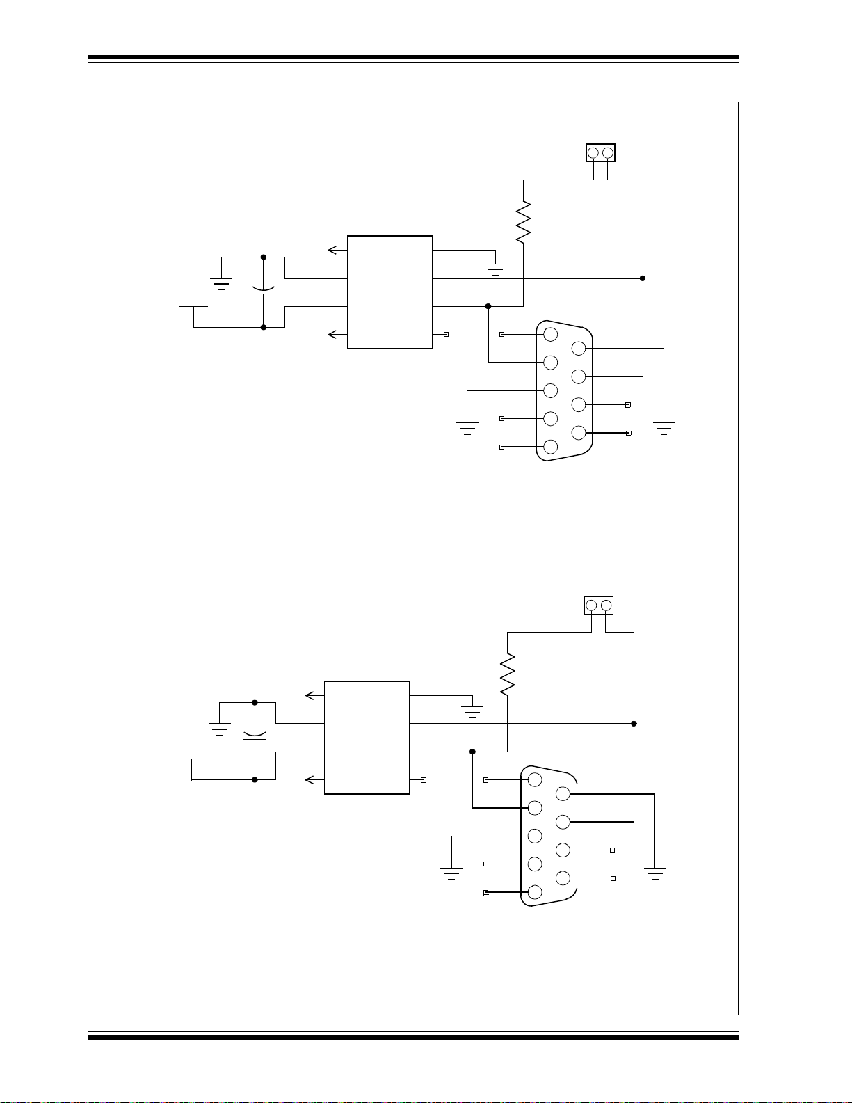
FIGURE A-5: LIN CIRCUIT SCHEMATICS
J12 used for Master/Slave select
J13 used for Master/Slave select
C1
10 uF
C2
10uF
D1
43V
D3
D5
D6
43V
D7
27V
D8
J8
LIN Power
+3.3V
+9V
LIN Power
LIN Power
R1
100k
R2
1k
R3
100k
R4
1k
J9
LIN Power
+12V
J10
J11
LIN Power
J12
J13
C3
22uF 25V
C4
0.1 uF
C7
0.1uF
C8
10uF
C9
10uF
C10
DNP
C11
DNP
D4
27V
+3.3V
U1
MCP2021
U2
MCP2021
1
2
3
1
2
1
2
3
1
2
3
Rxd
RF2/U1RX_E
CS/WAKE
RE8/INT1
VREG
Txd
RF3/U1TX_E
VSS
LIN
VBAT
FAULT/TXE
RD15/U1RTS_E
Rxd
RF4/PMPA9/U2RX
CS/WAKE
RA14/INT3
VREG
Txd
RF5/PMPA8/U2TX
VSS
LIN
VBAT
FAULT/TXE
RF13/U2RTS
LIN Power
LIN1
LIN2
Drawings and Schemati cs
2011 Microchip Technology Inc. DS70319B-page 27
Page 28
CAN/LIN/J2602 PICtail™ (Plus) Daughter Board User’s Guide
CAN1
C5
0.1uF
J4
J6
+5V
R5
120R
U3
MCP2551-DIP
9
8
7
6
1
2
3
4
5
TXD
RF1
VSS
VDD
RXD
RF0
VREF
CANL
CANH
RS
CAN2
C6
0.1uF
J5
J7
+5V
R6
120R
U4
MCP2551-DIP
9
8
7
6
1
2
3
4
5
TXD
RG1
VSS
VDD
RXD
RG0
VREF
CANL
CANH
RS
FIGURE A-6: CAN CIRCUIT SCHEMATICS
DS70319B-page 28 2011 Microchip Technology Inc.
Page 29

FIGURE A-7: CONNECTOR AND HEADER PINOUT SCHEMATICS
J1
J2
J3
+5V +5V
+5V +5V
+9V
+3.3V
+3.3V
+9V
+9V
+3.3V
+3.3V
+9V
+3.3V
+3.3V
+3.3V
+3.3V
+9V
+9V
+5V
+9V
+9V
+5V
+5V
+5V
117
118
111
112
105
106
99
100
93
94
87
88
81
82
75
76
69
70
57 58
51
RF12/U2CTS
52
RF13/U2RTS
45
RA9/PMPA7
46
RA10/PMPA6
39
RG8/PMPA3/SDO2
40
RA3/SDA2
33
RG9/PMPA2/SS2
34
RF4/PMPA9/U2RX
27
28
RF0
21
22
15
16
9
10
3
RF6/SCK1
4
RF3/U1TX_E
119 120
107
108
109
110
113
114
115
116
95
96
97
98
101
102
103
104
83
84
85
86
89
90
91
92
71
72
73
74
77
78
79
80
59
60
RG0
61
62
RG1
65
66
67
68
47 48
49
RA15/INT4
50
RA14/INT3
53 54
55 56
35
RG6/PMPA5/SCK2
36
RF5/PMPA8/U2TX
37
RG7/PMPA4/SDI2
38
RA2/SCL2
41
42
43
RB8/AN8
44
RB9/AN9
25
26
29
30
RF1
23
24
19
RD14/I1CTS_E
20
RD15/U1RTS_E
13
RB3/AN3
14
RB4/AN4
17
RE9/INT2
18
RE8/INT1
11
RB0/AN0
12
RB1/AN1
7
RF8/SDO1_E
8
RG3/SDA1
1
RB2/SS1/AN2
2
RF2/U1RX_E
5
RF7/SDI1_E
6
RG2/SCL1
29
25
23
RF12/U2CTS
19
RB8/AN8
17
RG8/PMPA3/SDO2
11
5
30
24
18
14
RG9/PMPA2/SS2
12
8
6
RB0/AN0
2
RF6/SCK1
27
15
RG6/PMPA5/SCK2
21
3
RF7/SDI1_E
7
RB3/AN3
9
RE9/INT2
13
1
RB2/SS1/AN2
28
20
RA9/PMPA7
22
RA15/INT4
26
16
RG7/PMPA4/SDI2
4
RF8/SDO1_E
10
RD14/I1CTS_E
29
RG0
25
RF13/U2RTS
23
19
RA3/SDA2
17
RF5/PMPA8/U2TX
11
5
30
RG1
24
RA14/INT3
18
RA2/SCL2
14
RF0
12
8
6
RB1/AN1
2
RF3/U1TX_E
27
15
RF1
21
RB9/AN9
3
RG2/SCL1
7
RB4/AN4
9
RE8/INT1
13
1
RF2/U1RX_E
28
20
22
RA10/PMPA6
26
16
RF4/PMPA9/U2RX
4
RG3/SDA1
10
RD15/U1RTS_E
Drawings and Schemati cs
2011 Microchip Technology Inc. DS70319B-page 29
Page 30

CAN/LIN/J2602 PICtail™ (Plus) Daughter Board User’s Guide
Figure A-8: CAN/LIN/J2602 PICtail™ (Plus) DAUGHTER BOARD (AC164130)
DS70319B-page 30 2011 Microchip Technology Inc.
Page 31

CAN/LIN/J2602 PICtail™ (Plus)
DAUGHTER BOARD USER’S GUIDE
Index
B
Board Layout............................................................23
C
CAN Bus Connectors...............................................18
CAN Bus Termination Jumpers................................18
CAN Circuits .......................................................26, 28
CAN Operation......................................................... 14
CAN Transceivers....................................................14
Customer Notification Service....................................8
Customer Support......................................................9
D
Documentation
Conventions........................................................6
Layout................................................................. 5
E
External Power Supply.............................................15
H
Hardware Components............................................16
Headers ................................................................... 15
I
Internet Address.........................................................7
L
LIN Bus Connectors.................................................17
LIN Operation...........................................................13
LIN Power Supply Terminal Block............................17
LIN Transceiver Power Supply Select Jumper.........17
LIN Transceivers......................................................13
M
Microchip Internet Web Site.......................................7
P
PICtail connector......................................................17
R
Reading, Recommended...........................................7
Readme .....................................................................7
Reference 1 .............................................................16
Reference 10 ...........................................................16
Reference 11 ...........................................................16
Reference 13 ...........................................................16
Reference 16 ...........................................................16
Reference 17 ...........................................................16
Reference 18 ...........................................................16
Reference 19 ...........................................................16
Reference 2 .............................................................16
Reference 3 .............................................................16
Reference 4..............................................................16
Reference 5..............................................................16
Reference 6..............................................................16
Reference 7..............................................................16
Reference 8..............................................................16
Reference 9..............................................................16
S
Schematics....................................................24, 26, 28
Connector Pinouts............................................29
Header Pinouts.................................................29
LIN Circuits .................................................25
Sleep Mode..............................................................14
, 27
W
Warranty Registration........................................ ...... ..7
WWW Address...........................................................7
2011 Microchip Technology Inc. DS70319B-page 31
Page 32

Worldwide Sales and Service
AMERICAS
Corporate Office
2355 West Chandler Blvd.
Chandler, AZ 85224-6199
Tel: 480-792-7200
Fax: 480-792-7277
Technical Support:
http://www.microchip.com/
support
Web Address:
www.microchip.com
Atlanta
Duluth, GA
Tel: 678-957-9614
Fax: 678-957-1455
Boston
Westborough, MA
Tel: 774-760-0087
Fax: 774-760-0088
Chicago
Itasca, IL
Tel: 630-285-0071
Fax: 630-285-0075
Cleveland
Independence, OH
Tel: 216-447-0464
Fax: 216-447-0643
Dallas
Addison, TX
Tel: 972-818-7423
Fax: 972-818-2924
Detroit
Farmington Hills, MI
Tel: 248-538-2250
Fax: 248-538-2260
Indianapolis
Noblesville, IN
Tel: 317-773-8323
Fax: 317-773-5453
Los Angeles
Mission Viejo, CA
Tel: 949-462-9523
Fax: 949-462-9608
Santa Clara
Santa Clara, CA
Tel: 408-961-6444
Fax: 408-961-6445
Toronto
Mississauga, Ontario,
Canada
Tel: 905-673-0699
Fax: 905-673-6509
ASIA/PACIFIC
Asia Pacific Office
Suites 3707-14, 37th Floor
Tower 6, The Gateway
Harbour City, Kowloon
Hong Kong
Tel: 852-2401-1200
Fax: 852-2401-3431
Australia - Sydney
Tel: 61-2-9868-6733
Fax: 61-2-9868-6755
China - Beijing
Tel: 86-10-8528-2100
Fax: 86-10-8528-2104
China - Chengdu
Tel: 86-28-8665-5511
Fax: 86-28-8665-7889
China - Chongqing
Tel: 86-23-8980-9588
Fax: 86-23-8980-9500
China - Hong Kong SAR
Tel: 852-2401-1200
Fax: 852-2401-3431
China - Nanjing
Tel: 86-25-8473-2460
Fax: 86-25-8473-2470
China - Qingdao
Tel: 86-532-8502-7355
Fax: 86-532-8502-7205
China - Shanghai
Tel: 86-21-5407-5533
Fax: 86-21-5407-5066
China - Shenyang
Tel: 86-24-2334-2829
Fax: 86-24-2334-2393
China - Shenzhen
Tel: 86-755-8203-2660
Fax: 86-755-8203-1760
China - Wuhan
Tel: 86-27-5980-5300
Fax: 86-27-5980-5118
China - Xian
Tel: 86-29-8833-7252
Fax: 86-29-8833-7256
China - Xiamen
Tel: 86-592-2388138
Fax: 86-592-2388130
China - Zhuhai
Tel: 86-756-3210040
Fax: 86-756-3210049
ASIA/PACIFIC
India - Bangalore
Tel: 91-80-3090-4444
Fax: 91-80-3090-4123
India - New Delhi
Tel: 91-11-4160-8631
Fax: 91-11-4160-8632
India - Pune
Tel: 91-20-2566-1512
Fax: 91-20-2566-1513
Japan - Yokohama
Tel: 81-45-471- 6166
Fax: 81-45-471-6122
Korea - Daegu
Tel: 82-53-744-4301
Fax: 82-53-744-4302
Korea - Seoul
Tel: 82-2-554-7200
Fax: 82-2-558-5932 or
82-2-558-5934
Malaysia - Kuala Lumpur
Tel: 60-3-6201-9857
Fax: 60-3-6201-9859
Malaysia - Penang
Tel: 60-4-227-8870
Fax: 60-4-227-4068
Philippines - Manila
Tel: 63-2-634-9065
Fax: 63-2-634-9069
Singapore
Tel: 65-6334-8870
Fax: 65-6334-8850
Tai wan - Hsin Chu
Tel: 886-3-6578-300
Fax: 886-3-6578-370
Taiwan - Kaohsiung
Tel: 886-7-213-7830
Fax: 886-7-330-9305
Taiwan - Taipei
Tel: 886-2-2500-6610
Fax: 886-2-2508-0102
Thailand - Bangkok
Tel: 66-2-694-1351
Fax: 66-2-694-1350
EUROPE
Austria - Wels
Tel: 43-7242-2244-39
Fax: 43-7242-2244-393
Denmark - Copenhagen
Tel: 45-4450-2828
Fax: 45-4485-2829
France - Paris
Tel: 33-1-69-53-63-20
Fax: 33-1-69-30-90-79
Germany - Munich
Tel: 49-89-627-144-0
Fax: 49-89-627-144-44
Italy - Milan
Tel: 39-0331-742611
Fax: 39-0331-466781
Netherlands - Drunen
Tel: 31-416-690399
Fax: 31-416-690340
Spain - Madrid
Tel: 34-91-708-08-90
Fax: 34-91-708-08-91
UK - Wokingham
Tel: 44-118-921-5869
Fax: 44-118-921-5820
02/18/11
DS70319B-page 32 2011 Microchip Technology Inc.
 Loading...