

Page 1

Bluetooth® Stereo Audio Module
BM62/64
Features
• Qualified for Bluetooth v5.0 specification
• Supports A2DP 1.3, AVRCP 1.6, HFP 1.7.2, HSP
1.2 and SPP 1.2
• Supports Bluetooth 5.0 dual-mode (BDR/EDR/
BLE) specifications
• Stand-alone module with on-board PCB antenna
and Bluetooth stack
• Supports high resolution up to 24-bit, 96 kHz
audio data format
• Supports Bluetooth Low Energy data rate up to
1Mbits/s
• Supports connection of two hosts with HFP/A2DP
profiles simultaneously
• Transparent UART mode for seamless serial data
over UART interface
• Supports virtual UART communication between
host MCU and smartphone applications by Bluetooth SPP or BLE link
• Easy to configure with Windows
by external MCU
• Supports firmware field upgrade
• Supports one microphone
• Compact surface mount module:
- BM62: 29 x 15 x 2.5 mm
- BM64: 32 x 15 x 2.5 mm
• Castellated surface mount pads for easy and
reliable host PCB mounting
• RoHS compliant
• Ideal for portable battery-operated devices
• Internal battery regulator circuitry
®
GUI or directly
• Supports Serial Copy Management System
(SCMS-T) content protection
FIGURE 1: BM62 MODULE
FIGURE 2: BM64 MODULE
DSP Audio Processing
• Supports 64 kbps A-Law, -Law PCM format/
Continuous Variable Slope Delta (CVSD) modulation for SCO channel operation
• Supports 8/16 kHz noise suppression
• Supports 8/16 kHz echo cancellation
• Supports Modified Sub-Band Coding (MSBC)
decoder for wide band speech
• Built-in High Definition Clean Audio (HCA) algorithms for both narrow band and wide band
speech processing
• Packet loss concealment (PLC)
• Built-in audio effect algorithms to enhance audio
streaming
2021 Microchip Technology Inc. Advanced DS60001403G-Page 1
Audio Codec
• Sub-band Coding (SBC) and optional Advanced
Audio Coding (AAC) decoding
• 20-bit Digital-to-Analog Converter (DAC) with
98 dB SNR
• 16-bit Analog-to-Digital Converter (ADC) with
92 dB SNR
• Supports up to 24-bit, 96 kHz I
(BM64 only)
2
S digital audio
Page 2

BM62/64
Peripherals
• Built-in lithium-ion and lithium-polymer battery
charger (up to 350 mA)
• Integrated 1.8V and 3V configurable switching
regulator and Low-Dropout (LDO) regulator
• Built-in ADC for battery monitoring and voltage
sense
• Built-in ADC for charger thermal protection
• Built-in Undervoltage Protection (UVP)
• An auxiliary input port for external audio input
• Two LED drivers
• Multiple I/O pins for control and status
RF/Analog
• Frequency spectrum: 2.402 GHz to 2.480 GHz
• Receive sensitivity: -90 dBm (2 Mbps EDR)
• Output Power
- BM64 Class 1: +15 dBm typical
- BM62/64 Class 2: +2 dBm typical
HCI Interface
• High-speed HCI-UART interface (supports up to
921,600 bps)
Description
The BM62/64 Stereo Audio module is a fully qualified
Bluetooth v5.0 dual-mode (BDR/EDR/BLE) module for
designers to add wireless audio and voice applications
to their products. The BM62/64 module is a Bluetooth
SIG-certified module that provides a complete wireless
solution with a Bluetooth stack, an integrated PCB
antenna, and worldwide radio certifications in a
compact surface-mount package.
The BM62/64 module has several SKUs. The BM62
module is a Class 2 device and the BM64 module is
available in both Class 1 and Class 2 versions.
MAC/Baseband Processor
• Supports Bluetooth 5.0 dual-mode
- BDR/EDR transport for audio, voice, and
SPP data exchange
- BLE transport for proprietary transparent
service and Apple Notification Center Service
(ANCS) data exchange
Operating Condition
• Operating voltage: 3.2V to 4.2V
• Operating temperature: -20°C to +70°C
Compliance
• Bluetooth Special Interest Group (SIG) QDID:
110148 (BM62, BM64 Class 2) and 110159
(BM64 Class 1)
• Certified to the United States (FCC), Innovation,
Science and Economic Development Canada
(ISED), European Economic Area (CE), Korea
(KCC), Taiwan (NCC), Japan (MIC), China
(SRRC), and Brazil (ANATEL) radio regulations
Applications
• Portable speaker
• Multiple speakers
• Headset
DS60001403G-Page 2 Advanced 2021 Microchip Technology Inc.
Page 3

BM62/64
Table of Contents
1.0 Device Overview ....................................................................................................................................................... 6
2.0 Audio....................................................................................................................................................................... 15
3.0 Transceiver ............................................................................................................................................................. 20
4.0 Power Management Unit ........................................................................................................................................ 22
5.0 Application Information .......................................................................................................................................... 25
6.0 Printed Antenna Information .................................................................................................................................. 43
7.0 Physical Dimensions.............................................................................................................................................. 46
8.0 Electrical Characteristics........................................................................................................................................ 50
9.0 Soldering Recommendations ................................................................................................................................. 58
10.0 Ordering Information ............................................................................................................................................ 59
Appendix A: Certification Notices................................................................................................................................. 60
Appendix B: Revision History....................................................................................................................................... 70
TO OUR VALUED CUSTOMERS
It is our intention to provide our valued customers with the best documentation possible to ensure successful use of your Microchip
products. To this end, we will continue to improve our publications to better suit your needs. Our publications will be refined and
enhanced as new volumes and updates are introduced.
If you have any questions or comments regarding this publication, please contact the Marketing Communications Department via
E-mail at docerrorsmicrochip.com or fax the Reader Response Form in the back of this data sheet to (480) 792-4150. We welcome your feedback.
Most Current Data Sheet
To obtain the most up-to-date version of this data sheet, please register at our Worldwide Web site at:
http://www.microchip.com
You can determine the version of a data sheet by examining its literature number found on the bottom outside corner of any page.
The last character of the literature number is the version number, (e.g., DS30000000A is version A of document DS30000000).
Errata
An errata sheet, describing minor operational differences from the data sheet and recommended workarounds, may exist for current
devices. As device/documentation issues become known to us, we will publish an errata sheet. The errata will specify the revision
of silicon and revision of document to which it applies.
To determine if an errata sheet exists for a particular device, please check with one of the following:
• Microchip’s Worldwide Web site; http://www.microchip.com
• Your local Microchip sales office (see last page)
When contacting a sales office, please specify which device, revision of silicon and data sheet (include literature number) you are
using.
Customer Notification System
Register on our web site at www.microchip.com to receive the most current information on all of our products.
2021 Microchip Technology Inc. Advanced DS60001403G-Page 3
Page 4
BM62/64
1.0 DEVICE OVERVIEW
The BM62 and BM64 Stereo Audio modules are built
around Microchip Technology IS2062 and IS2064
SoCs.
The IS2062/64 SoC integrates the Bluetooth 5.0 dualmode radio transceiver, Power Management Unit
(PMU), a crystal and DSP. Users can configure the
BM62/64 module by using the UI tool and DSP tool, a
Windows-based utility.
Note: The UI and DSP tools are available for
download from the Microchip website at:
www.microchip.com/BM62 and
www.microchip.com/BM64.
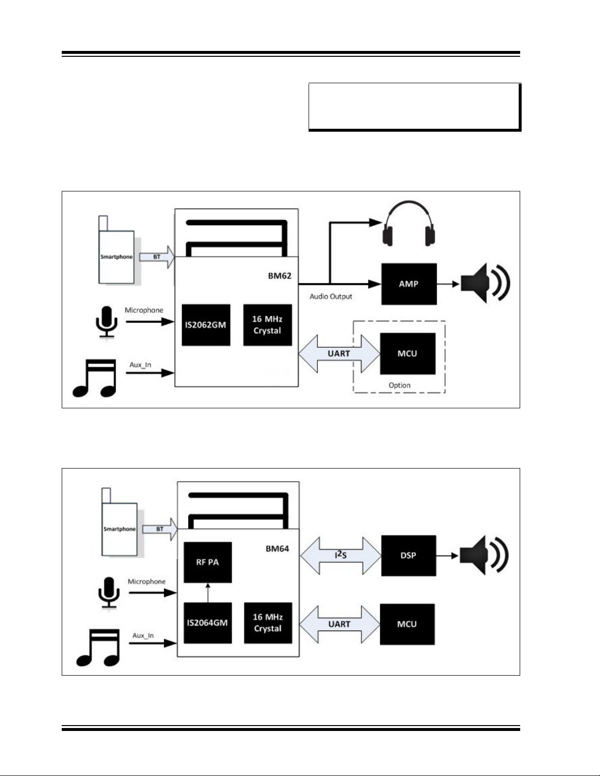
Figure 1-1 illustrates a typical example of the BM62
module, which is connected to an external audio
amplifier and the MCU.
FIGURE 1-1: SINGLE SPEAKER APPLICATION USING BM62 MODULE
Figure 1-2 illustrates a typical example of the Class 1
BM64 module, which is connected to an external MCU
and a DSP/codec.
FIGURE 1-2: SINGLE SPEAKER APPLICATION USING BM64 MODULE
DS60001403G-Page 4 Advanced 2021 Microchip Technology Inc.
Page 5
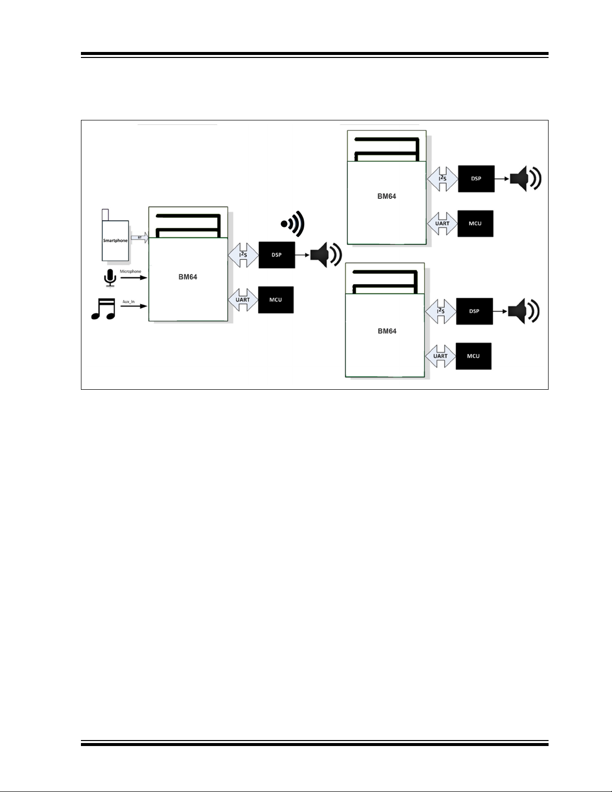
Figure 1-3 illustrates the multi-speaker application
using the BM64 module.
FIGURE 1-3: MULTI-SPEAKER APPLICATION USING BM64 MODULE
BM62/64
2021 Microchip Technology Inc. Advanced DS60001403G-Page 5
Page 6
BM62/64
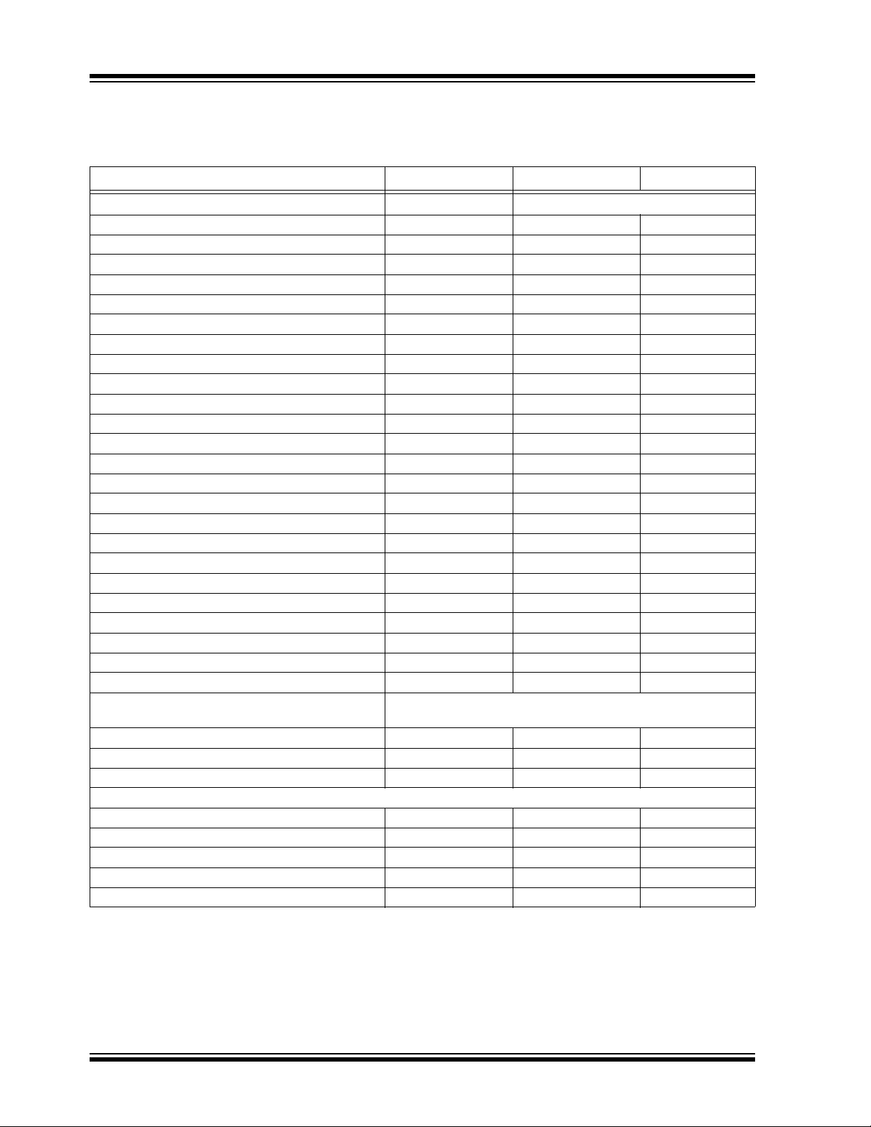
Table 1-1 provides the key features of the BM62/64
module.
TABLE 1-1: BM62/64 KEY FEATURES
Feature BM62 CLASS 2 BM64 CLASS 2 BM64 CLASS 1
Application Headset/Speaker Multi-Speaker/Soundbar
Stereo/mono Stereo Stereo Stereo
Pin count 37 43 43
Dimensions (mm
PCB antenna Yes Yes Yes
Tx power (typical) 2 dBm 2 dBm 15 dBm
Audio DAC output 2-channel 2-channel 2-channel
DAC (single-ended) SNR at 2.8V (dB) -98 -98 -98
DAC (capless) SNR at 2.8V (dB) -98 -98 -98
ADC SNR at 2.8V (dB) -92 -92 -92
2
I
S digital output No Yes Yes
Analog Auxiliary-Input Yes Yes Yes
Mono microphone 1 1 1
External audio amplifier interface Yes Yes Yes
UART Yes Yes Yes
Full-speed USB 1.1 No Yes Yes
LED driver 2 2 2
Internal DC-DC step down regulator Yes Yes Yes
DC 5V adapter input Yes Yes Yes
Battery charger (350 mA max) Yes Yes Yes
ADC for thermal charger protection Yes Yes Yes
Under voltage protection (UVP) Yes Yes Yes
GPIO 10 12 12
Button support 6 6 6
EEPROM Yes Yes Yes
Customized voice prompt 8K Sampling Rate, Stored in EEPROM with approximately
Multitone Yes Yes Yes
DSP functions (audio playback and voice call) Yes Yes Yes
BLE Yes Yes Yes
Bluetooth profiles
A2DP 1.3 1.3 1.3
AVRCP 1.6 1.6 1.6
HFP 1.7.2 1.7.2 1.7.2
HSP 1.2 1.2 1.2
SPP 1.2 1.2 1.2
2
) 15 x 29 15 x 32 15 x 32
800 bytes/second
DS60001403G-Page 6 Advanced 2021 Microchip Technology Inc.
Page 7
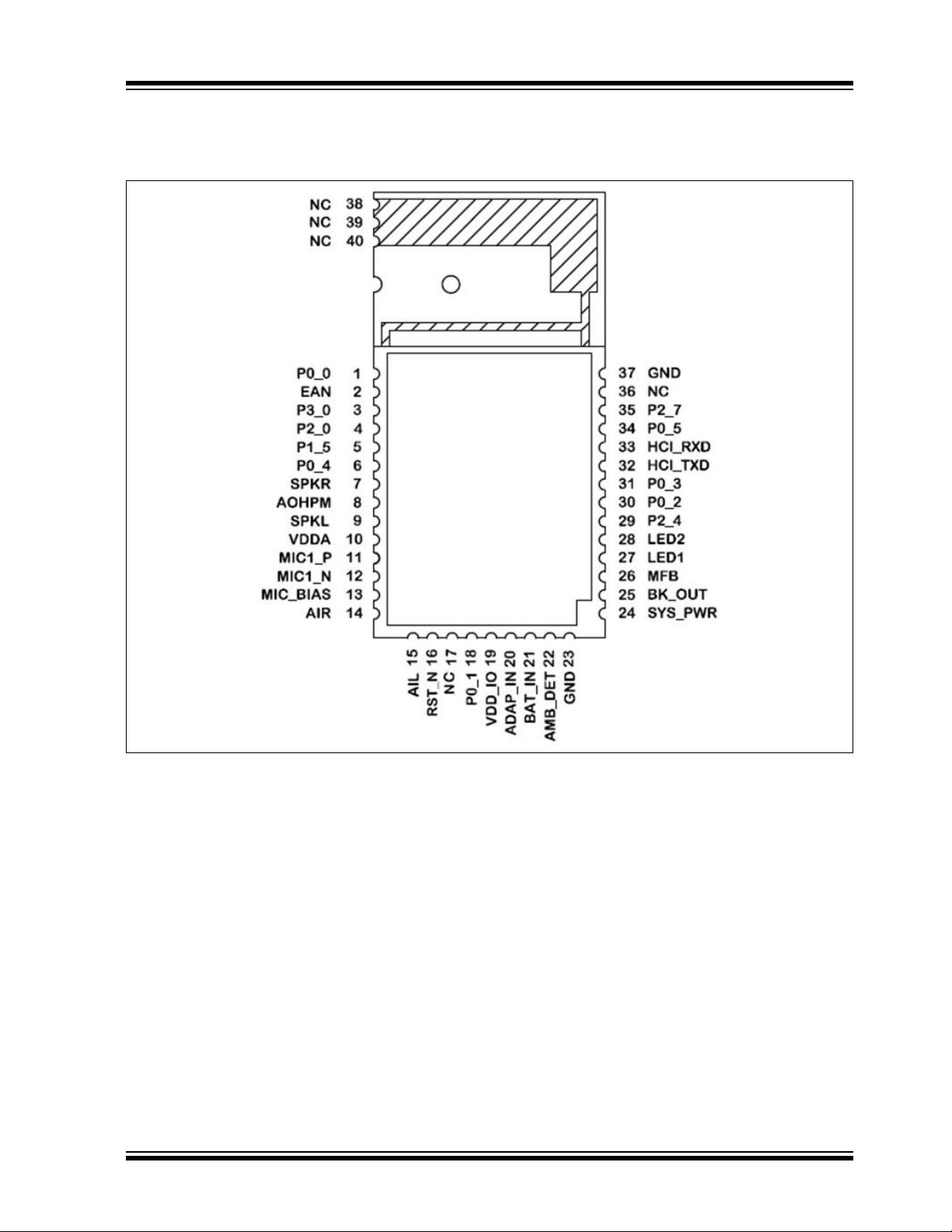
Figure 1-4 illustrates the pin diagram of the BM62
module.
FIGURE 1-4: BM62 MODULE PIN DIAGRAM
BM62/64
2021 Microchip Technology Inc. Advanced DS60001403G-Page 7
Page 8

BM62/64
Table 1-2 provides the pin description of the BM62
module.
TABLE 1-2: BM62 MODULE PIN DESCRIPTION
Pin No Pin Type Pin Name Description
1 I/O P0_0 Configurable control or indication pin
(Internally pulled up, if configured as an input)
• Slide switch detector, active-high
• UART TX_IND, active-low (used by Bluetooth system to wakeup the host MCU)
2 I EAN External address bus negative
System configuration pin along with the P2_0 and
P2_4 pins, used to set the module in any one of the following three modes:
• Application mode (for normal operation)
• Test mode (to change EEPROM values)
• Write Flash mode (to load a new firmware into the
module), refer to Ta b le 5 -1
Flash type module already installed internal pull down
resistor 4.7 kOhm to GND
3 I/O P3_0 Configurable control or indication pin
(Internally pulled up, if configured as an input)
Auxiliary input detector, active-low
4 I/O P2_0 System configuration pin along with P2_4 and EAN
pins used to set the module in any one of the following
three modes:
• Application mode (for normal operation)
• Test mode (to change EEPROM values)
• Write Flash mode (to load a new firmware into the
module), refer to Ta b le 5 -1
5 I/O P1_5 Configurable control or indication pin
(Internally pulled up, if configured as an input)
• NFC detection pin, active-low
• Out_Ind_1
• Slide switch detector, active-high
6 I/O P0_4 Configurable control or indication pin
(Internally pulled up, if configured as an input)
• NFC detection pin, active-low
• Out_Ind_1
7 O SPKR Right-channel, analog headphone output
8 O AOHPM Headphone common mode output/sense input
9 O SPKL Left-channel, analog headphone output
10 P VDDA Analog reference voltage. Do not connect, for internal
use only
11 I MIC1_P MIC1 mono differential analog positive input
12 I MIC1_N MIC1 mono differential analog negative input
13 P MIC1_BIAS Electric microphone biasing voltage
14 I AIR Right-channel, single-ended analog input
15 I AIL Left-channel, single-ended analog input
Legend: I= Input pin O= Output pin I/O= Input/Output pin P= Power pin
Note: All I/O pins can be configured using the UI tool, a Windows utility.
DS60001403G-Page 8 Advanced 2021 Microchip Technology Inc.
Page 9
BM62/64
TABLE 1-2: BM62 MODULE PIN DESCRIPTION (CONTINUED)
Pin No Pin Type Pin Name Description
16 I RST_N System Reset (active-low)
17 - NC No connection
18 I/O P0_1 Configurable control or indication pin
(Internally pulled up, if configured as an input)
• FWD key when Class 2 RF (default), active-low
• Class 1 Tx control signal for external RF Tx/Rx
switch, active-high
19 P VDD_IO I/O positive supply. Do not connect, for internal use
only
20 P ADAP_IN 5V power adapter input, used to charge the battery in
the Li-Ion battery power applications
21 P BAT_IN Power Supply input.
Voltage range: 3.2V to 4.2V. Source can either be a
Li-Ion battery or any other power rail on the host board
22 P AMB_DET Analog input for ambient temperature detection
23 P GND Ground reference
24 P SYS_PWR System power output derived from ADAP_IN or
BAT_IN. Refer to reference schematic for external connection.
25 P BK_OUT 1.8V buck regulator output. Do not connect to other
devices. For internal use only
26 I MFB • Multi-Function Button and power-on key
• UART RX_IND, active-high (used by host MCU to
wakeup the Bluetooth system)
27 O LED1 LED driver 1
28 O LED2 LED driver 2
29 I/O P2_4 System configuration pin along with P2_0 and EAN
pins used to set the module in any one of the following
three modes:
• Application mode (for normal operation)
• Test mode (to change EEPROM values)
• Write Flash mode (to load a new firmware into the
module), refer to Ta b le 5 -1
30 I/O P0_2 Configurable control or indication pin
(Internally pulled up, if configured as an input)
Play/Pause key (default), active-low
31 I/O P0_3
32 I/O HCI_TXD HCI UART data output
33 I/O HCI_RXD HCI UART data input
Legend: I= Input pin O= Output pin I/O= Input/Output pin P= Power pin
Note: All I/O pins can be configured using the UI tool, a Windows utility.
Configurable control or indication pin
(Internally pulled up, if configured as an input)
• REV key (default), active-low
• Buzzer signal output
• Out_Ind_2
• Class 1 Rx Control signal of external RF Tx/Rx
switch, active-high
2021 Microchip Technology Inc. Advanced DS60001403G-Page 9
Page 10
BM62/64
TABLE 1-2: BM62 MODULE PIN DESCRIPTION (CONTINUED)
Pin No Pin Type Pin Name Description
34 I/O P0_5
35 I/O P2_7
36 - NC No connection
37 P GND Ground reference
38 - NC No connection
39 - NC No connection
40 - NC No connection
Legend: I= Input pin O= Output pin I/O= Input/Output pin P= Power pin
Note: All I/O pins can be configured using the UI tool, a Windows utility.
Configurable control or indication pin
(Internally pulled up, if configured as an input)
Volume-down key (default), active-low
Configurable control or indication pin
(Internally pulled up, if configured as an input)
Volume-up key (default), active-low
DS60001403G-Page 10 Advanced 2021 Microchip Technology Inc.
Page 11
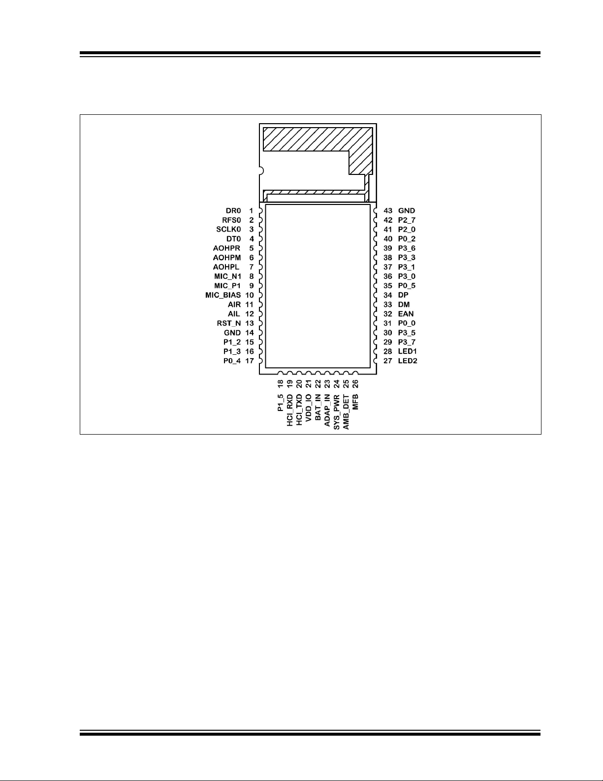
Figure 1-5 illustrates the pin diagram of the BM64
module.
FIGURE 1-5: BM64 MODULE PIN DIAGRAM
BM62/64
2021 Microchip Technology Inc. Advanced DS60001403G-Page 11
Page 12
BM62/64
Table 1-3 provides the pin description of the BM64
Module.
TABLE 1-3: BM64 MODULE PIN DESCRIPTION
Pin No Pin Type Pin Name Description
2
1 I/O DR0 I
2I/ORFS0I
3I/OSCLK0I
4I/ODT0I
5 O AOHPR Right-channel, analog headphone output
6 O AOHPM Headphone common mode output/sense input
7 O AOHPL Left-channel, analog headphone output
8 I MIC_N1 MIC1 mono differential analog negative input
9 I MIC_P1 MIC1 mono differential analog positive input
10 P MIC_BIAS Electric microphone biasing voltage
11 I AIR Right-channel, single-ended analog input
12 I AIL Left-channel, single-ended analog input
13 I RST_N System Reset (active-low)
14 P GND Ground reference
15 I/O P1_2 EEPROM clock SCL
16 I/O P1_3 EEPROM data SDA
17 I/O P0_4
18 I/O P1_5
19 I HCI_RXD HCI-UART data input
20 O HCI_TXD HCI-UART data output
21 P VDD_IO I/O positive supply. Do not connect, for internal use only
22 P BAT_IN Power Supply input.
23 P ADAP_IN 5V power adapter input, used to charge the battery in the
24 P SYS_PWR System power output derived from ADAP_IN or BAT_IN.
25 P AMB_DET Analog input for ambient temperature detection
26 I MFB • Multi-Function Button and power-on key
27 O LED2 LED driver 2
28 O LED1 LED driver 1
Legend: I= Input pin O= Output pin I/O= Input/Output pin P= Power pin
Note: All I/O pins can be configured using the UI tool, a Windows utility.
S interface: digital left/right data
2
S interface: left/right clock
2
S interface: bit clock
2
S interface: digital left/right data
Configurable control or indication pin
(Internally pulled up, if configured as an input)
• NFC detection pin, active-low
• Out_Ind_1
Configurable control or indication pin
(Internally pulled up, if configured as an input)
• NFC detection pin, active-low
• Slide switch detector, active-high
• Out_Ind_1
• Multi-SPK Central/Peripheral mode control (firmware
dependent)
Voltage range: 3.2V to 4.2V. Source can either be a Li-Ion battery or any other power rail on the host board
Li-Ion battery power applications
Refer to reference schematic for external connection.
• UART RX_IND, active-high (used by host MCU to
wakeup the Bluetooth system)
DS60001403G-Page 12 Advanced 2021 Microchip Technology Inc.
Page 13
BM62/64
TABLE 1-3: BM64 MODULE PIN DESCRIPTION (CONTINUED)
Pin No Pin Type Pin Name Description
29 I/O P3_7
30 I/O P3_5 Configurable control or indication pin
31 I/O P0_0
32 I EAN External address bus negative
33 I/O DM Differential data-minus USB
34 I/O DP Differential data-plus USB
35 I/O P0_5
36 I/O P3_0
37 I/O P3_1
38 I/O P3_3
39 I/O P3_6
40 I/O P0_2
41 I/O P2_0 System configuration pin along with EAN pins used to set the
42 I/O P2_7
43 P GND Ground reference
Legend: I= Input pin O= Output pin I/O= Input/Output pin P= Power pin
Note: All I/O pins can be configured using the UI tool, a Windows utility.
Configurable control or indication pin
(Internally pulled up, if configured as an input)
UART TX_IND, active-low (used by Bluetooth system to
wakeup the host MCU)
(Internally pulled low, if configured as an input)
• Slide switch detector, active-high
Configurable control or indication pin
(Internally pulled up, if configured as an input)
• Slide switch detector, active-high, Out_Ind_0
System configuration pin along with the P2_0 pins used to set
the module in any one of these modes:
• Application mode (for normal operation)
• Test mode (to change FW and EEPROM values)
• Mode setting, refer to Ta bl e 5- 1
Flash type module already installed internal pull down resistor
4.7 kOhm to GND
Configurable control or indication pin
(Internally pulled up, if configured as an input)
Volume-down key (default), active-low
Configurable control or indication pin
(Internally pulled up, if configured as an input)
Auxiliary input detector, active-low
Configurable control or indication pin
(Internally pulled up, if configured as an input)
REV key (default), active-low
Configurable control or indication pin
(Internally pulled up, if configured as an input)
FWD key (default), active-low
Configurable control or indication pin
(Internally pulled up, if configured as an input)
Multi-SPK Central/Peripheral mode control (firmware dependent)
Configurable control or indication pin
(Internally pulled up, if configured as an input)
Play/Pause key (default)
module in any one of the following modes:
• Application mode (for normal operation)
• Test mode (to change FW and EEPROM values)
• Mode setting, refer to Ta bl e 5- 1
Configurable control or indication pin
(Internally pulled up, if configured as an input)
Volume-up key (default), active-low
2021 Microchip Technology Inc. Advanced DS60001403G-Page 13
Page 14

BM62/64
NOTES:
DS60001403G-Page 14 Advanced 2021 Microchip Technology Inc.
Page 15
BM62/64
2.0 AUDIO
The input and output audios have different stages and
each stage can be programmed to vary the gain
response characteristics. For microphone, both single-ended inputs and differential inputs are supported.
To maintain a high quality signal, a stable bias voltage
source to the condenser microphone’s FET is provided.
The DC blocking capacitors can be used at both positive and negative sides of an input. Internally, this
analog signal is converted to 16-bit, 8/16 kHz linear
PCM data.
2.1 Digital Signal Processor
A Digital Signal Processor (DSP) is used to perform
speech and audio processing. The advanced speech
features, such as acoustic echo cancellation and noise
reduction are inbuilt. To reduce nonlinear distortion and
to help echo cancellation, an outgoing signal level to
FIGURE 2-1: SPEECH SIGNAL PROCESSING
the speaker is monitored and adjusted to avoid
saturation of speaker output or microphone input.
Adaptive filtering is also applied to track the echo path
impulse in response to provide echo free and
full-duplex user experience.
The embedded noise reduction algorithm helps to
extract clean speech signals from the noisy inputs
captured by the microphones and improves mutual
understanding in communication.
The advanced audio features, such as multi-band
dynamic range control, parametric multi-band equalizer, audio widening and virtual bass are inbuilt. The
audio effect algorithms improve the user’s audio
listening experience in terms of better audio quality
after audio signal processing.
Figure 2-1 and Figure 2-2 illustrate the processing flow
of speakerphone applications for speech and audio signal processing.
FIGURE 2-2: AUDIO SIGNAL PROCESSING
2021 Microchip Technology Inc. Advanced DS60001403G-Page 15
Page 16
BM62/64
Note: The data corresponds to the 16 Ohm load with 2.8V operating voltage at +25°C room temperature.
Note: The data corresponds to the 16 Ohm load with 2.8V operating voltage at +25°C room temperature.
The DSP parameters can be configured using the DSP
tool. For additional information on the DSP tool, refer to
the “IS206X DSP Application Note”.
Note: The DSP tool and “IS206X DSP Applica-
tion Note” document, are available for
download from the Microchip website at:
www.microchip.com/BM62 and
www.microchip.com/BM64.
FIGURE 2-3: CODEC DAC DYNAMIC RANGE
2.2 Codec
The built-in codec has a high signal-to-noise ratio
(SNR) performance and it consists of an ADC, a DAC
and an additional analog circuitry.
Note: The internal codec supports 16-bit resolu-
tion; by adding trailing zeros in LSBs
2
24-bit I
Figure 2-3 through Figure 2-6 illustrate the dynamic
range and frequency response of the codec.
S port requirements can be met.
FIGURE 2-4: CODEC DAC THD+N VERSUS INPUT POWER
DS60001403G-Page 16 Advanced 2021 Microchip Technology Inc.
Page 17
FIGURE 2-5: CODEC DAC FREQUENCY RESPONSE (CAPLESS MODE)
Note: The DAC frequency response corresponds to Single-ended mode with a 47 μF DC block capacitor.
BM62/64
FIGURE 2-6: CODEC DAC FREQUENCY RESPONSE (SINGLE-ENDED MODE)
2021 Microchip Technology Inc. Advanced DS60001403G-Page 17
Page 18
BM62/64
2.3 Auxiliary Port
The BM62/64 module supports one analog (line-in) signal from the external audio source. The analog (line-in)
signal can be processed by the DSP to generate
different sound effects (multi-band dynamic range
compression and audio widening), which can be
configured by using the DSP tool.
2.4 Analog Speaker Output
The BM62/64 module supports the following analog
speaker output modes:
• Capless mode — Recommended for headphone
applications in which capless output connection
helps to save the BOM cost by avoiding a large
DC blocking capacitor. Figure 2-7 illustrates the
analog speaker output capless mode.
• Single-ended mode — Used for driving an external audio amplifier where a DC blocking capacitor
is required. Figure 2-8 illustrates the analog
speaker output single-ended mode.
FIGURE 2-7: ANALOG SPEAKER OUTPUT CAPLESS MODE
FIGURE 2-8: ANALOG SPEAKER OUTPUT SINGLE-ENDED MODE
DS60001403G-Page 18 Advanced 2021 Microchip Technology Inc.
Page 19

NOTES:
BM62/64
2021 Microchip Technology Inc. Advanced DS60001403G-Page 19
Page 20

BM62/64
3.0 TRANSCEIVER
The BM62/64 module is designed and optimized for the
Bluetooth 2.4 GHz system. It contains a complete radio
frequency transmitter/receiver section. An internal synthesizer generates a stable clock for synchronizing with
another device.
3.1 Transmitter
The internal power amplifier (PA) has a maximum output power of +4 dBm. This is applied for Class 2 or
Class 3 radios without an external RF PA.
The transmitter performs the IQ conversion to minimize
the frequency drift.
3.2 Receiver
The Low-Noise Amplifier (LNA) operates with TR-combined mode for single port application. It can save a pin
on the package without having an external Tx/Rx
switch.
The ADC is used to sample the input analog signal and
convert it into a digital signal for demodulator analysis.
A channel filter has been integrated into the receiver
channel before the ADC, which is used to reduce the
external component count and increase the anti-interference capability.
The image rejection filter is used to reject the image frequency for low-IF architecture. This filter for low-IF
architecture is intended to reduce external Band Pass
Filter (BPF) component for a super heterodyne
architecture.
The Received Signal Strength Indicator (RSSI) signal
feedback to the processor is used to control the RF
output power to make a good trade-off for effective
distance and current consumption.
BDR, symbol 1 represents 1-bit. However, each symbol in the payload part of EDR packet represents 2/3
bits. This is achieved by using two different modulations, π/4 DQPSK and 8 DPSK.
3.5 Adaptive Frequency Hopping
(AFH)
The BM62/64 module has an AFH function to avoid RF
interference. It has an algorithm to check the nearby
interference and to choose clear channel for
transceiver Bluetooth signal.
3.3 Synthesizer
A synthesizer generates a clock for radio transceiver
operation. There is a VCO inside with a tunable internal
LC tank that can reduce variation for components. A
crystal oscillator with an internal digital trimming circuit
provides a stable clock for the synthesizer.
3.4 Modem
For Bluetooth 1.2 specification and below, 1 Mbps was
the standard data rate based on the Gaussian Frequency Shift Keying (GFSK) modulation scheme. This
basic rate modem meets Basic Data Rate (BDR)
requirements of Bluetooth 2.0 with Enhanced Data
Rate (EDR) specifications.
For Bluetooth 2.0 and above specifications, EDR has
been introduced to provide the data rates of
1/2/3 Mbps. For baseband, both BDR and EDR utilize
the same 1 MHz symbol rate and 1.6 kHz slot rate.
DS60001403G-Page 20 Advanced 2021 Microchip Technology Inc.
For
Page 21

NOTES:
BM62/64
2021 Microchip Technology Inc. Advanced DS60001403G-Page 21
Page 22
BM62/64
4.0 POWER MANAGEMENT UNIT
The on-chip Power Management Unit (PMU) has two
main features: lithium-ion and lithium-polymer battery
charger, and voltage regulator. A power switch is used
to switch over the power source between the battery
and an adapter. Also, the PMU provides current to
drive two LEDs.
FIGURE 4-1: BATTERY CHARGING CURVE
4.1 Charging a Battery
The BM62/64 module has a built-in battery charger,
which is optimized for lithium-ion and lithium-polymer
batteries.
The battery charger includes a current sensor for
charging control, user-programmable current regulation, and high accuracy voltage regulation.
The charging current parameters are configured by the
UI tool. Reviving, pre-charging, constant current and
constant voltage modes, and re-charging functions are
included. The maximum charging current is 350 mA.
Figure 4-1 illustrates the charging curve of a battery.
4.2 Voltage Monitoring
A 10-bit, successive approximation register ADC (SAR
ADC) provides a dedicated channel for battery voltage
level detection. The warning level can be programmed
by using the UI tool. The ADC provides a granular resolution to enable the external MCU to take control over
the charging process.
DS60001403G-Page 22 Advanced 2021 Microchip Technology Inc.
4.3 LED Drivers
Two dedicated LED drivers control the LEDs.They provide enough sink current (16 step control and 0.35 mA
for each step), thus LEDs can be connected directly
with the BM62/64 module. The LED settings can be
configured using the UI tool.
Page 23

Figure 4-2 illustrates the LED drivers in the BM62/64
module.
FIGURE 4-2: LED DRIVERS
4.4 Under Voltage Protection (Software Dependent UVP)
BM62/64
When the input voltage of the BAT_IN is below 2.9V,
the system will not be able to start up, in order to protect
the system.
4.5 Ambient Detection
The BM62/64 module has a built-in ADC for charger
thermal protection. Figure 4-3 illustrates the suggested
circuit and thermistor, Murata NCP15WF104F. The
charger thermal protection can avoid battery charge in
restricted temperature range. The upper and lower
limits for temperature values can be configured by
using the UI tool.
Note: Thermistor must be placed close to the
battery in the user application for accurate
temperature measurements and to enable
the thermal shutdown feature.
2021 Microchip Technology Inc. Advanced DS60001403G-Page 23
Page 24

BM62/64
FIGURE 4-3: AMBIENT DETECTION
DS60001403G-Page 24 Advanced 2021 Microchip Technology Inc.
Page 25

BM62/64
5.0 APPLICATION INFORMATION
5.1 Power Supply
The following figure illustrates the connection from the
BAT_IN pin to various other voltage supply pins of the
IS2062/64 SoC.
FIGURE 5-1: POWER TREE DIAGRAM
The IS2062/64 SoC is powered through the BAT_IN
input pin. The external 5V power adapter can be connected to ADAP_IN in order to charge the battery.
5.2 Host MCU Interface
The BM62/64 module supports UART commands. The
UART commands enable an external MCU to control
the BM62/64 module. Figure 5-2 illustrates the UART
interface between the BM62/64 module and an external MCU.
FIGURE 5-2: HOST MCU INTERFACE OVER UART
An external MCU can control the BM62/64 module over
the UART interface and wake-up the module with the
MFB, P0_0 (BM62) and P3_7 (BM64) pins.
2021 Microchip Technology Inc. Advanced DS60001403G-Page 25
Page 26

BM62/64
Refer to the “UART_CommandSet” document for a list
of functions the BM62/64 module supports and how to
use the UI tool to configure the UART and UART Command Set tool.
Note: The UART Command set tool (SPKCom-
mandSetTool v160.xx) and “UART_Com-
mandSet” document are available for
download from the Microchip website at:
www.microchip.com/BM62 and
www.microchip.com/BM64.
DS60001403G-Page 26 Advanced 2021 Microchip Technology Inc.
Page 27

2021 Microchip Technology Inc. Advanced DS60001403G-Page 27
Figure 5-3 through Figure 5-8 illustrate the timing sequences of various UART
control signals.
FIGURE 5-3: POWER-ON/OFF SEQUENCE
BM62/64
Page 28

BM62/64
Note 1: EEPROM clock = 100 kHz.
2: For a byte write: 0.01 ms x 32 clock x 2 = 640 μs.
3: It is recommended to have ramp-down time more than 640 μs during the power-off sequence to
ensure safe operation of the device.
FIGURE 5-4: TIMING SEQUENCE OF RX INDICATION AFTER POWER-ON STATE
FIGURE 5-5: TIMING SEQUENCE OF POWER-OFF STATE
DS60001403G-Page 28 Advanced 2021 Microchip Technology Inc.
Page 29

FIGURE 5-6: TIMING SEQUENCE OF POWER-ON (NACK)
Note: When the host MCU sends the UART command and the BM62/64 module does not respond, the
MCU resends the UART command. If the BM62/64 module does not respond within 5 secs, the MCU
will force the system to Reset.
BM62/64
FIGURE 5-7: RESET TIMING SEQUENCE IN NO RESPONSE FROM MODULE TO HOST MCU
2021 Microchip Technology Inc. Advanced DS60001403G-Page 29
Page 30

BM62/64
Note 1: It is recommended to use the battery to provide the power supply at BAT_IN in to the module.
2: If an external power source or a power adapter is utilized to provide power to the module (BAT_IN), it is
recommended to use a voltage supervisor IC.
3: The Reset IC output pin, RST_N, must be “Open drain” type and threshold voltage as 2.93V.
4: The RST_N signal must be fully pulled low before BAT_IN power drop to 2.7V
FIGURE 5-8: TIMING SEQUENCE OF POWER DROP PROTECTION
5.2.1 DEVICE FW UPGRADE (DFU)
After receiving all the images and storing in local
memory, such as SPI flash/USB thumb drive, the MCU
conducts the DFU for BT Module.
5.2.1.1 Enter BT Module/MCU DFU mode
To upgrade the flash through UART, first select the
module in “ROM TEST” mode.
The timing for BM64 to enter “ROM TEST” mode is
illustrated in following figure (P20 low and EAN high).
FIGURE 5-9: Timing Diagram of Application Mode to DFU Mode
Be sure to switch back from “ROM TEST/DFU” mode
to Application mode, after the DFU, as illustrated in following figure.
DS60001403G-Page 30 Advanced 2021 Microchip Technology Inc.
Page 31

FIGURE 5-10: Timing Diagram of DFU Mode to Application Mode
5.3 I2S Mode Application
The BM64 module provides an I
interface to connect with an external codec/DSP. It provides 8, 16, 44.1, 48, 88.2, and 96 kHz sampling rates
for 16-bit and 24-bit data formats. The I
be configured by using the UI and DSP tools.
2
S digital audio output
2
S setting can
Figure 5-11 and Figure 5-12 illustrate the I
connection between the BM64 module and an external
DSP. Use the DSP tool to configure the BM64 module
as a host/client.
For additional information on timing specifications,
refer to 8.1 “Timing Specifications”.
BM62/64
2
S signal
FIGURE 5-11: BM64 MODULE IN I2S HOST MODE
2021 Microchip Technology Inc. Advanced DS60001403G-Page 31
Page 32

BM62/64
FIGURE 5-12: BM64 MODULE IN I2S CLIENT MODE
5.4 Reset
The BM62/64 module provides a Watchdog Timer
(WDT) to reset the chip. It has an integrated Power-on
Reset (POR) circuit that resets all circuits to a known
power-on state. This action can be driven by an external reset signal, which is used to control the device
externally by forcing it into a POR state. The RST_N
signal input is active-low and no connection is required
in most applications.
DS60001403G-Page 32 Advanced 2021 Microchip Technology Inc.
Page 33

5.5 External Configuration and Programming
The BM62/64 module can be configured by using an
external configuration tool (EEPROM tool) and the firmware is programmed by using a programming tool
(Flash tool).
Note: The EEPROM and Flash tools are avail-
able for download from the Microchip web
site at: www.microchip.com/BM62 and
www.microchip.com/BM64.
Figure 5-13 illustrates the configuration and firmware
programming interface on the BM62 module. It is
recommended to include a header pin on the main PCB
for development.
FIGURE 5-13: EXTERNAL PROGRAMMING HEADER CONNECTIONS
BM62/64
2021 Microchip Technology Inc. Advanced DS60001403G-Page 33
Page 34

BM62/64
The Configuration and Firmware programming modes
are entered according to the system configuration I/O
pins. Ta bl e 5- 1 provides the system configuration settings.
TABLE 5-1: SYSTEM CONFIGURATION I/O PIN SETTINGS
Pins
P2_0 EAN P2_4
High Low High Flash Application
High High High ROM Application
Low Low High Flash IBDK
Low High High ROM IBDK
Low High Low Boot
Note 1: The P2_0, P2_4 and EAN pins have internal pull high.
2: Boot mode is not supported in the BM64 module, as the P2_4 pin does not exist on the module.
Bluetooth Mode
DS60001403G-Page 34 Advanced 2021 Microchip Technology Inc.
Page 35

2021 Microchip Technology Inc. Advanced DS60001403G-Page 35
5.6 Reference Circuit
Figure 5-14 through Figure 5-17 illustrate the BM62 module reference circuit for
a stereo headset applications.
FIGURE 5-14: BM62 REFERENCE CIRCUIT FOR STEREO HEADSET APPLICATION
BM62/64
Page 36

DS60001403G-Page 36 Advanced 2021 Microchip Technology Inc.
FIGURE 5-15: BM62 REFERENCE CIRCUIT FOR STEREO HEADSET APPLICATION
BM62/64
Page 37

BM62/64
Note: The section “NFC (Optional)” contains built-in rectifier circuit of NXP 203F NFC type.
FIGURE 5-16: BM62 REFERENCE CIRCUIT FOR STEREO HEADSET APPLICATION
2021 Microchip Technology Inc. Advanced DS60001403G-Page 37
Page 38

BM62/64
Note: All ESD diodes in the schematics are reserved for testing.
FIGURE 5-17: BM62 REFERENCE CIRCUIT FOR STEREO HEADSET APPLICATION
DS60001403G-Page 38 Advanced 2021 Microchip Technology Inc.
Page 39

2021 Microchip Technology Inc. Advanced DS60001403G-Page 39
Figure 5-18 through Figure 5-21 illustrate the BM64 reference circuit for a
stereo headset applications.
FIGURE 5-18: BM64 REFERENCE CIRCUIT FOR STEREO HEADSET APPLICATION
BM62/64
Page 40

DS60001403G-Page 40 Advanced 2021 Microchip Technology Inc.
FIGURE 5-19: BM64 REFERENCE CIRCUIT FOR STEREO HEADSET APPLICATION
BM62/64
Page 41

BM62/64
FIGURE 5-20: BM64 REFERENCE CIRCUIT FOR STEREO HEADSET APPLICATION
2021 Microchip Technology Inc. Advanced DS60001403G-Page 41
Page 42

BM62/64
FIGURE 5-21: BM64 REFERENCE CIRCUIT FOR STEREO HEADSET APPLICATION
DS60001403G-Page 42 Advanced 2021 Microchip Technology Inc.
Page 43

6.0 PRINTED ANTENNA INFORMATION
6.1 Antenna Radiation Pattern
The BM62/64 module is integrated with one PCB printed
antenna, see Figure 6-1.
FIGURE 6-1: RECOMMENDED KEEPOUT AREA FOR PCB ANTENNA
BM62/64
2021 Microchip Technology Inc. Advanced DS60001403G-Page 43
Page 44

BM62/64
Figure 6-2 illustrates the 3D radiation pattern of the
PCB printed antenna at 2441 MHZ.
FIGURE 6-2: PCB ANTENNA 3D RADIATION PATTERN AT 2441 MHZ
Table 6-1 provides the PCB Antenna characteristics of
the BM62/64 module.
TABLE 6-1: BM62/64 PCB ANTENNA
CHARACTERISTICS
Parameter Values
Frequency 2400 MHz to 2480 MHz
Peak Gain 1.927 dBi
Efficiency 73.41%
6.2 Mod ule Placement Guidelines
For a Bluetooth-enabled product, the antenna placement
affects the overall performance of the system. The
antenna requires free space to radiate RF signals and it
must not be surrounded by the ground plane. Microchip
recommends that the areas underneath the antenna on
the host PCB must not contain copper on the top, inner, or
bottom layers, as illustrated in Figure 6-1.
A low-impedance ground plane
performance (best range, lowest noise). The ground
plane can be extended beyond the minimum
recommendation, as required for the main PCB EMC
will ensure the best radio
noise reduction. For the best range performance, keep all
external metal at least 15 mm away from the on-board
PCB trace antenna.
DS60001403G-Page 44 Advanced 2021 Microchip Technology Inc.
Page 45

Figure 6-3 and Figure 6-4 illustrate the examples of
good and poor placement of the BM62/64 module on a
host board with GND plane.
FIGURE 6-3: MODULE PLACEMENT GUIDELINES
BM62/64
FIGURE 6-4: GND PLANE ON MAIN APPLICATION BOARD
2021 Microchip Technology Inc. Advanced DS60001403G-Page 45
Page 46

BM62/64
Note: PCB dimensions: X: 15.0 mm, Y: 29.0 mm and tolerances: 0.25 mm.
7.0 PHYSICAL DIMENSIONS
Figure 7-1 illustrates the PCB dimension of the BM62
module.
FIGURE 7-1: BM62 MODULE PCB DIMENSION
DS60001403G-Page 46 Advanced 2021 Microchip Technology Inc.
Page 47

Figure 7-2 illustrates the PCB dimension of the BM64
Note: PCB dimensions: X: 15.0 mm, Y: 32.0 mm and tolerances: 0.25 mm.
module.
FIGURE 7-2: BM64 MODULE PCB DIMENSION
BM62/64
2021 Microchip Technology Inc. Advanced DS60001403G-Page 47
Page 48

BM62/64
Note 1: The keep-out area is reserved to keep the RF test point away from GND plane.
2: All metal keep-out is used to isolate the PCB antenna.
Figure 7-3 illustrates the recommended PCB footprint
of the BM62 module.
FIGURE 7-3: RECOMMENDED BM62 MODULE PCB FOOTPRINT
DS60001403G-Page 48 Advanced 2021 Microchip Technology Inc.
Page 49

Figure 7-4 illustrates the recommended PCB footprint
Note 1: The keep-out area is reserved to keep the RF test point away from GND plane.
2: All metal keep-out is used to isolate the PCB antenna.
of the BM64 module.
FIGURE 7-4: RECOMMENDED BM64 MODULE PCB FOOTPRINT
BM62/64
2021 Microchip Technology Inc. Advanced DS60001403G-Page 49
Page 50

BM62/64
8.0 ELECTRICAL CHARACTERISTICS
This section provides an overview of the BM62/64 Stereo Audio module electrical characteristics. Additional
information will be provided in future revisions of this document, as it becomes available.
Absolute maximum ratings for the BM62/64 module are listed below.
Absolute Maximum Ratings
Ambient temperature under bias...............................................................................................................-20°C to +70°C
Storage temperature ...............................................................................................................................-40°C to +125°C
Voltage on V
Maximum output current sink by any I/O pin..........................................................................................................12 mA
Maximum output current sourced by any I/O pin....................................................................................................12 mA
Note: Stresses listed under “Absolute Maximum Ratings” may cause permanent damage to the device. This
DD with respect to VSS ......................................................................................................... -0.3V to +3.6V
is a stress rating only. The functional operation of the device at those or any other conditions and those
indicated in the operation listings of this specification, is not implied. Exposure to maximum rating conditions for extended periods may affect device reliability.
DS60001403G-Page 50 Advanced 2021 Microchip Technology Inc.
Page 51

BM62/64
Table 8-1 through Ta b le 8 -9 provide the recommended
operating conditions and the electrical specifications of
the BM62/64 module.
TABLE 8-1: RECOMMENDED OPERATING CONDITION
Symbol Parameter Min. Typ. Max. Unit
BAT_IN Input voltage for battery 3.2 3.8 4.2 V
ADAP_IN Input voltage for adapter 4.5 5 5.5 V
T
OPERATION Operation temperature -20 +25 +70 ºC
Note: The absolute and recommended operating condition tables reflect a typical voltage usage for the device.
TABLE 8-2: I/O AND RESET LEVEL
Parameter Min. Typ. Max. Unit
I/O Supply Voltage (VDD_IO) 3.0 3.3 3.6 V
I/O Voltage Levels
V
input logic levels low 0 — 0.8 V
IL
V
input logic levels high 2.0 — 3.6 V
IH
V
output logic levels low — — 0.4 V
OL
V
output logic levels high 2.4 — — V
OH
RST_N Input Low to High
Threshold Point
Input High to Low
Threshold Point
Threshold voltage — 1.6 — V
Note: These parameters are characterized, but not tested in manufacturing.
— — 1.87 V
1.25 — — V
TABLE 8-3: BATTERY CHARGER
Parameter Min. Typ. Max. Unit
ADAP_IN Input Voltage 4.5 5.0 5.5 V
Supply current to charger only — 3 4.5 mA
Maximum Battery
Fast Charge Current
Trickle Charge Voltage Threshold
Battery Charge Termination Current,
(% of Fast Charge Current)
Note 1: Headroom = VADAP_IN – VBAT
2: When VADAP_IN – VBAT > 2V, the maximum fast charge current is 175 mA for thermal protection.
3: These parameters are characterized, but not tested in manufacturing.
Headroom > 0.7V
(ADAP_IN = 5V)
Headroom = 0.3V to 0.7V
(ADAP_IN = 4.5V)
— 350 — mA
— 175
—3—V
—10—%
(2)
—mA
2021 Microchip Technology Inc. Advanced DS60001403G-Page 51
Page 52

BM62/64
TABLE 8-4: LED DRIVER
Parameter Min. Typ. Max. Unit
Open-drain Voltage — — 3.6 V
Programmable Current Range 0 — 5.25 mA
Intensity Control — 16 — step
Current Step — 0.35 — mA
Power-Down Open-drain Current — — 1 μA
Shutdown Current — — 1 μA
Note 1: Test condition: BK_OUT = 1.8V with +25ºC temperature.
2: These parameters are characterized, but not tested in manufacturing.
TABLE 8-5: AUDIO CODEC ANALOG TO DIGITAL CONVERTER
T = 25oC, VDD = 2.8V, 1 kHz sine wave input, Bandwidth = 20 Hz to 20 kHz
Parameter (Condition) Min. Typ. Max. Unit
Resolution — — 16 Bit
Output Sample Rate 8 — 48 kHz
Signal-to-Noise Ratio (Note 1)
(SNR at MIC or Line-in mode)
Digital Gain -54 — 4.85 dB
Digital Gain Resolution — 2 to 6 — dB
MIC Boost Gain — 20 — dB
Analog Gain — — 60 dB
Analog Gain Resolution — 2.0 dB
Input full-scale at maximum gain (differential) — 4 — mV/rms
Input full-scale at minimum gain (differential) — 800 — mV/rms
3 dB bandwidth — 20 — kHz
Microphone mode (input impedance) — 24 — kOhm
THD+N (microphone input) at 30 mV/rms input — 0.02 — %
Note 1: f
in = 1 kHz, B/W = 20 Hz to 20 kHz, A-weighted, THD+N < 1%, 150 mVPP input.
2: These parameters are characterized, but not tested in manufacturing.
—92—dB
DS60001403G-Page 52 Advanced 2021 Microchip Technology Inc.
Page 53

BM62/64
TABLE 8-6: AUDIO CODEC DIGITAL TO ANALOG CONVERTER
T = 25oC, VDD = 2.8V, 1 kHz sine wave input, Bandwidth = 20 Hz to 20 kHz
Parameter (Condition) Min. Typ. Max. Unit
Over-sampling rate — 128 — f
Resolution 16 — 20 Bit
Output Sample Rate 8 — 48 kHz
Signal-to-Noise Ratio (Note 1)
(SNR at capless mode) for 48 kHz
Signal-to-Noise Ratio (Note 1)
(SNR at single-ended mode) for 48 kHz
Digital Gain -54 — 4.85 dB
Digital Gain Resolution — 2 to 6 — dB
Analog Gain -28 — 3 dB
Analog Gain Resolution — 1 — dB
Output Voltage Full-scale Swing (AV
Maximum Output Power (16 Ohm load) — 34.5 — mW
Maximum Output Power (32 Ohm load) — 17.2 — mW
Allowed Load Resistive — 16 O.C. Ohm
THD+N (16 Ohm load) (Note 2) —0.05—%
Signal-to-Noise Ratio (SNR at 16 Ohm load) (Note 3) —98—dB
Note 1: fin = 1 kHz, B/W = 20 Hz to 20 kHz, A-weighted, THD+N < 0.01%, 0 dBFS signal, Load = 100 kOhm
in
= 1 kHz, B/W = 20 Hz to 20 kHz, A-weighted, -1 dBFS signal, Load =16 Ohm
2: f
in = 1 kHz, B/W = 20 Hz to 20 kHz, A-weighted, THD+N < 0.05%, 0 dBFS signal, Load = 16 Ohm
3: f
4: These parameters are characterized, but not tested in manufacturing.
DD = 2.8V) 495 742.5 — mV/rms
Capacitive — — 500 pF
—98—dB
—98—dB
s
TABLE 8-7: TRANSMITTER SECTION FOR BDR AND EDR
Parameter Min. Typ. Max.
(3)
(3)
— < 20 dBm
— -6 to 4 dBm
RF transmit power
EDR/BDR Relative transmit power -4 -1.8 1 -4 to 1 dB
Note 1: The RF Tx power is modulation value.
2: The RF Transmit power is calibrated during the production by using the MP tool software and MT8852 Blue-
tooth test equipment.
3: Test condition: VCC_RF = 1.28V, temperature +25ºC.
Class 1 — 15.0
Class 2 — 2
Bluetooth
specification
Unit
2021 Microchip Technology Inc. Advanced DS60001403G-Page 53
Page 54

BM62/64
TABLE 8-8: RECEIVER SECTION FOR BDR AND EDR
Modulation Min. Typ. Max.
Sensitivity at 0.1% BER GFSK — -89 — ≤-70 dBm
Sensitivity at 0.01% BER π/4 DQPSK — -90 — ≤-70 dBm
8 DPSK — -83 — ≤-70 dBm
Note 1: Test condition: VCC_RF = 1.28V with temperature +25ºC.
2: These parameters are characterized, but not tested in manufacturing.
TABLE 8-9: BM62 SYSTEM CURRENT CONSUMPTION
System Status Typ.
System-Off mode — 10 μA
Stop advertising (Samsung S5 (SM-G900I)/Android™ 4.4.2)
Standby mode 0.57 — mA
Link mode 0.5 — mA
ESCO link 15.1 — mA
A2DP link 14.3 — mA
Stop advertising (iPhone
Standby mode 0.6 — mA
Link mode 0.6 — mA
SCO link 15.3 — mA
A2DP link 15.4 — mA
Note 1: The measurement data corresponds to Firmware v1.0.
2: Mode definition:
Standby mode: Power-on without Bluetooth link;
Link mode: With Bluetooth link in Low-power mode.
3: The current consumption values are measured with the BM62 EVB as test platform, with BAT_IN = 3.8V.
The distance between the smartphone and BM62 EVB is 30 cm, and the speaker is without loading.
®
6/iOS 8.4)
Bluetooth
specification
(1)
Unit
Max. Unit
TABLE 8-10: BM64SPKS1MC2 EMBEDDED MODE (WITHOUT EXTERNAL MCU) SYSTEM
CURRENT CONSUMPTION
Mode/System Status Typ.
System-Off mode 1.61 — μA
Standby mode 0.6 — mA
Pairing mode 1.2 — mA
Link mode 0.5 — mA
SCO link 15.8 — mA
A2DP link 14.5 — mA
Note 1: The current consumption values are measured with the BM64 EVB (in standalone mode without MCU) as
test platform, with BAT_IN = 3.8V. The distance between the smartphone and BM64 EVB is 30 cm, and the
speaker is without loading.
2: The measurement data corresponds to Firmware package: BM64 Software & Tools (DSPK v2.1), which is
available in https://www.microchip.com/wwwproducts/en/BM64.
3: LED and Bluetooth Low Energy advertising is turned off in UI setting.
4: iPhone6+, iOS 11.4.
DS60001403G-Page 54 Advanced 2021 Microchip Technology Inc.
(1)
Max. Unit
Page 55

BM62/64
TABLE 8-11: BM64SPKS1MC2 HOST MCU MODE SYSTEM CURRENT CONSUMPTION
Mode/System Status Typ.
System-Off mode 15.23 — μA
Standby mode 1.6 — mA
Pairing mode 3.2 — mA
Link mode 1.5 — mA
SCO link 18.8 — mA
A2DP link 17.5 — mA
Note 1: The current consumption values are measured with the BM64 EVB (with MCU: PIC18F85J10) as test plat-
form, with BAT_IN = 3.3V. The distance between the smartphone and BM64 EVB is 30 cm, and the speaker
is without loading.
2: Audio: I2S Digital Audio output to External Codec Yamaha YDA174.
3: The measurement data corresponds to Firmware package: BM64 Software & Tools (DSPK v2.1), which is
available in https://www.microchip.com/wwwproducts/en/BM64.
4: Bluetooth Low Energy advertising is turned off.
8.1 Timing Specifications
Figure 8-1 and Figure 8-2 illustrate the timing diagram
of the BM62/64 module in I2S and PCM modes.
.
(1)
Max. Unit
FIGURE 8-1: TIMING DIAGRAM FOR I2S MODES (HOST/CLIENT)
2021 Microchip Technology Inc. Advanced DS60001403G-Page 55
Page 56

BM62/64
Note 1: fs: 8,16, 32, 44.1, 48, 88.2 and 96 kHz.
2: SCLK0: 64*f
s
/256*fs.
3: Word Length: 16-bit and 24-bit.
FIGURE 8-2: TIMING DIAGRAM FOR PCM MODES (HOST/CLIENT)
Figure 8-3 illustrates the timing diagram of the audio
interface.
FIGURE 8-3: AUDIO INTERFACE TIMING DIAGRAM
Table 8-12 provides the timing specifications of the
audio interface.
TABLE 8-12: AUDIO INTERFACE TIMING SPECIFICATIONS
PARAMETER SYMBOL MIN TYP MAX UNIT
SCLK0 duty ratio d
SCLK0 cycle time t
SCLK0 pulse width high t
SCLK0 pulse width low t
RFS0 setup time to SCLK0 rising edge t
RFS0 hold time from SCLK0 rising edge t
DR0 hold time from SCLK0 rising edge t
Note: Test Conditions: Client mode, fs = 48 kHz, 24-bit data and SLK0 period = 256 fs.
SCLK
SCLKCY
SCLKCH
SCLKCL
RFSSU
RFSH
DH
—50—%
50 — — ns
20 — — ns
20 — — ns
10 — — ns
10 — — ns
10 — — ns
DS60001403G-Page 56 Advanced 2021 Microchip Technology Inc.
Page 57

NOTES:
BM62/64
2021 Microchip Technology Inc. Advanced DS60001403G-Page 57
Page 58

BM62/64
9.0 SOLDERING RECOMMENDATIONS
The BM62/64 module is assembled using a standard
lead-free reflow profile, IPC/JEDEC J-STD-020.
BM62/64 module can be soldered to the main PCB
using standard leaded and lead-free solder reflow
profiles.
To avoid the damage to the module, follow these recommendations:
• Refer to Microchip Technology Application Note
AN233 Solder Reflow Recommendation”
“
(DS00233) for the
recommendations.
soldering reflow
FIGURE 9-1: REFLOW PROFILE
The
• Do not exceed peak temperature (TP) of +260ºC.
• Refer to the “Solder Paste” data sheet for specific
reflow profile recommendations.
• Use no-clean flux solder paste.
• Do not wash the module, as moisture can be
trapped under the shield.
• Use only one flow. If the PCB requires multiple
flows, apply the module on the final flow.
Figure 9-1 illustrates the reflow profile of the BM62/64
module.
DS60001403G-Page 58 Advanced 2021 Microchip Technology Inc.
Page 59

BM62/64
10.0 ORDERING INFORMATION
Table 10-1 provides ordering information for the
BM62/64 module.
TABLE 10-1: BM62/64 MODULE ORDERING INFORMATION
Module Microchip IC Description Shield Regulatory Certification Part No.
BM62 IS2062GM Bluetooth 5.0 Stereo Audio module,
Class 2 with RF shield
BM62 IS2062GM Bluetooth 5.0 Stereo Audio module,
Class 2 without RF shield
BM64 IS2064GM Bluetooth 5.0 Stereo Audio module,
Class 2 with RF shield
BM64 IS2064GM Bluetooth 5.0 Stereo Audio module,
Class 2 without RF shield
BM64 IS2064GM Bluetooth 5.0 Stereo Audio module,
Class 1 with RF shield
BM64 IS2064GM Bluetooth 5.0 Stereo Audio module,
Class 1 without RF shield
Note: The BM62/64 module can be purchased through a Microchip representative. Visit www.microchip.com for
the current pricing and a list of distributors for the product.
Yes FCC, ISED, CE, MIC, KCC,
NCC, SRRC
No CE BM62SPKA1MC2
Yes FCC, ISED, CE, MIC, KCC,
NCC, SRRC, ANATEL
No CE BM64SPKA1MC2
Yes FCC, ISED, CE, MIC, KCC,
NCC, SRRC, ANATEL
No CE BM64SPKA1MC1
BM62SPKS1MC2
BM64SPKS1MC2
BM64SPKS1MC1
2021 Microchip Technology Inc. Advanced DS60001403G-Page 59
Page 60

BM62/64
APPENDIX A: CERTIFICATION
NOTICES
The BM62 module (BM62SPKS1MC2) has received
regulatory approval for the following countries:
• BT SIG/QDID: 110148
• United States/FCC ID: A8TBM62S2
• Canada/ISED
- IC: 12246A-BM62S2
- HVIN: BM62SPKS1MC2
• Europe/CE
• Japan/MIC: 005-101204
• Korea/KCC: MSIP-CRM-mcp-BM62SPKS1MC2
• Taiwan/NCC No: CCAN16LP0270T5
• China/SRRC: CMIIT ID: 2016DJ2656
The BM64C1 (Class 1) module (BM64SPKS1MC1)
has received regulatory approval for the following
countries:
• BT SIG/QDID: 110159
• United States/FCC ID: A8TBM64S1
• Canada/ISED
- IC: 12246A-BM64S1
- HVIN: BM64SPKS1MC1
• Europe/CE
• Japan/MIC: 005-101206
• Korea/KCC: MSIP-CRM-mcp-BM64SPKS1MC1
• Taiwan/NCC No: CCAN16LP0300T1
• China/SRRC: CMIIT ID: 2016DJ2453
• Brazil/ANATEL: 05784-19-08759
The BM64C2 (Class 2) module (BM64SPKS1MC2)
has received regulatory approval for the following
countries:
• BT SIG/QDID: 110148
• United States/FCC ID: A8TBM64S2
• Canada/ISED
- IC: 12246A-BM64S2
- HVIN: BM64SPKS1MC2
• Europe/CE
• Japan/MIC: 005-101205
• Korea/KCC: MSIP-CRM-mcp-BM64SPKS1MC2
• Taiwan/NCC No: CCAN16LP0280T8
• China/SRRC: CMIIT ID: 2016DJ2356
• Brazil/ANATEL: 03822-18-08759
A.1 REGULATORY APPROVAL
This section outlines the regulatory information of the
BM62/BM64C1/BM64C2 Stereo Audio modules for the
following countries:
• United States
• Canada
• Europe
• Japan
• Korea
•Taiwan
• China
• Brazil
• Other Regulatory Jurisdictions
A.1.1 UNITED STATES
The BM62/BM64C1/BM64C2 Stereo Audio module has
received Federal Communications Commission (FCC)
CFR47
tional Radiators” single-modular approval in accordance with
Single-modular transmitter approval is defined as a
complete RF transmission sub-assembly, designed to
be incorporated into another device, that must
demonstrate compliance with FCC rules and policies
independent of any host. A transmitter with a modular
grant can be installed in different end-use products
(referred to as a host, host product, or host device) by
the grantee or other equipment manufacturer, then the
host product may not require additional testing or
equipment authorization for the transmitter function
provided by that specific module or limited module
device.
The user must comply with all of the instructions provided by the Grantee, which indicate installation and/or
operating conditions necessary for compliance.
The host product itself is required to comply with all other
applicable FCC equipment authorizations regulations,
requirements and equipment functions that are not
associated with the transmitter module portion. For
example, compliance must be demonstrated: to regulations for other transmitter components within a
product; to requirements for unintentional radiators
(Part 15 Subpart B),
peripherals, radio receivers, etc.; and to additional
authorization requirements for the non-transmitter functions on the transmitter module (i.e., Verification, or
Declaration of Conformity) as appropriate (e.g., Bluetooth and Wi-Fi transmitter modules may also contain
digital logic functions).
Telecommunications, Part 15 Subpart C “Inten-
Part 15.212 Modular Transmitter approval.
host
such as digital devices, computer
A.1.2 LABELING AND USER
INFORMATION REQUIREMENTS
The BM62/BM64C1/BM64C2 Stereo Audio module has
been labeled with its own FCC ID number, and if the
FCC ID is not visible when the module is installed inside
another device, then the outside of the finished product
into which the
label referring to the enclosed module. This exterior
label can use
module is installed must also display a
wording as follows:
DS60001403G-Page 60 Advanced 2021 Microchip Technology Inc.
Page 61

BM62/64
For the BM62:
Contains Transmitter Module FCC ID: A8TBM62S2
or
Contains FCC ID: A8TBM62S2
This device complies with Part 15 of the FCC
Rules. Operation is subject to the following two
conditions: (1) this device may not cause harmful
interference, and (2) this device must accept any
interference received, including interference that
may cause undesired operation
For the BM64C1:
Contains Transmitter Module FCC ID: A8TBM64S1
or
Contains FCC ID: A8TBM64S1
This device complies with Part 15 of the FCC
Rules. Operation is subject to the following two
conditions: (1) this device may not cause harmful
interference, and (2) this device must accept any
interference received, including interference that
may cause undesired operation
For the BM64C2:
Contains Transmitter Module FCC ID: A8TBM64S2
or
Contains FCC ID: A8TBM64S2
This device complies with Part 15 of the FCC
Rules. Operation is subject to the following two
conditions: (1) this device may not cause harmful
interference, and (2) this device must accept any
interference received, including interference that
may cause undesired operation
A user’s manual for the product must include the following statement:
This equipment has been tested and found to comply
with the limits for a Class B digital device, pursuant to
part 15 of the FCC Rules. These limits are designed
to provide reasonable protection against harmful
interference in a residential installation. This equipment generates, uses and can radiate radio frequency energy, and if not installed and used in
accordance with the instructions, may cause harmful
interference to radio communications. However,
there is no guarantee that interference will not occur
in a particular installation. If this equipment does
cause harmful interference to radio or television
reception, which can be determined by turning the
equipment off and on, the user is encouraged to try to
correct the interference by one or more of the following measures:
• Reorient or relocate the receiving antenna
• Increase the separation between the equipment
and receiver
• Connect the equipment into an outlet on a circuit
different from that to which the receiver is connected
• Consult the dealer or an experienced radio/TV
technician for help
Additional information on labeling and user information
requirements for Part 15 devices can be found in KDB
Publication 784748, which is available at the FCC
Office of Engineering and Technology (OET) Laboratory Division Knowledge Database (KDB)
https://apps.fcc.gov/oetcf/kdb/index.cfm
A.1.3 RF EXPOSURE
All transmitters regulated by FCC must comply with RF
exposure requirements. KDB 447498 General RF
Exposure Guidance provides guidance in determining
whether proposed or existing transmitting facilities,
operations or devices comply with limits for human
exposure to Radio Frequency (RF) fields adopted by
the Federal Communications Commission (FCC).
From the FCC Grant: Output power listed is conducted.
This grant is valid only when the module is sold to OEM
integrators and must be installed by the OEM or OEM
integrators. This transmitter is restricted for use with
the specific antenna(s) tested in this application for
Certification and must not be co-located or operating in
conjunction with any other antenna or transmitters
within a host device, except in accordance with FCC
multi-transmitter product procedures.
BM62 and BM64C2: These modules are approved for
installation into mobile or/and portable host platforms.
BM64C1:The installation of the transmitter must ensure
that the antenna has a separation distance of at least
30 mm from all persons or compliance, and it must be
demonstrated according to the FCC SAR procedures.
2021 Microchip Technology Inc. Advanced DS60001403G-Page 61
Page 62

BM62/64
A.1.4 APPROVED ANTENNAS
To maintain modular approval in the United States, only
the antenna types that have been tested shall be used.
It is permissible to use different antenna, provided the
same antenna type, antenna gain (equal to or less
than), with similar in-band and out-of band characteristics (refer to specification sheet for cutoff frequencies).
For BM62/BM64C1/BM64C2, the approval is received
using the antenna listed in Table 6-1.
A.1.5 HELPFUL WEB SITES
Federal Communications Commission (FCC):
https://www.fcc.gov/
FCC Office of Engineering and Technology (OET) Laboratory Division Knowledge Database (KDB):
https://apps.fcc.gov/oetcf/kdb/index.cfm
A.2 Canada
The BM62/BM64C1/BM64C2 Stereo Audio module
has been certified for use in Canada under Innovation,
Science and Economic Development Canada (ISED,
formerly Industry Canada) Radio Standards Procedure
(RSP) RSP-100, Radio Standards Specification (RSS)
RSS-Gen and RSS-247. Modular approval permits the
installation of a module in a host device without the
need to rectify the device.
A.2.1 LABELING AND USER
INFORMATION REQUIREMENTS
Labeling Requirements (from RSP-100, Issue 12, Section 5): The host product shall be properly labeled to
identify the module within the host device.
The Innovation, Science and Economic Development
Canada certification label of a module shall be clearly
visible at all times when installed in the host product,
otherwise the host device must be labeled to display
the Innovation, Science and Economic Development
Canada certification number of the module, preceded
by the word “Contains”, or similar word expressing the
same meaning, as follows:
For the BM62:
Contains IC: 12246A-BM62S2
For the BM64C1:
Contains IC: 12246A-BM64S1
For the BM64C2:
Contains IC: 12246A-BM64S2
User Manual Notice for License-Exempt Radio Apparatus (from Section 8.4 RSS-Gen, Issue 5, March 2019):
User manuals for license-exempt radio apparatus shall
contain the following or equivalent notice in a conspicuous location in the user manual or alternatively on the
device or both:
This device contains license-exempt transmitters)/receiver(s) that comply with Innovation, Science and Economic Development Canada’s
license-exempt RSS (s). Operation is subject to
the following two conditions:
• This device may not cause interference;
• This device must accept any interference,
including interference that may cause undesired operation of the device.
L’émetteur/récepteur exempt de licence contenu
dans le présent appareil est conforme aux CNR
d’Innovation,SciencesetDéveloppement
économique Canada applicables aux appareils
radio exempts de licence. L’exploitation est
autorisée aux deux conditions suivantes:
• L’appareil ne doit pas produire de brouillage;
• L’appareil doit accepter tout brouillage
radioélectrique subi, même si le brouillage
est susceptible d’en compromettre le
fonctionnement.
Transmitter Antenna (From Section 6.8 RSS-GEN,
Issue 5, March 2019): User manuals, for transmitters
shall display the following notice in a conspicuous location:
This radio transmitter [IC: 12246A-BM62S2, IC:
12246A-BM64S1 and IC: 12246A-BM64S2] has
been approved by Innovation, Science and Economic Development Canada to operate with the
antenna types listed below, with the maximum
permissible gain indicated. Antenna types not
included in this list that have a gain greater than
the maximum gain indi- cated for any type listed
are strictly prohibited for use with this device.
Le présent émetteur radio
[IC: 12246A-BM62S2, IC: 12246A-BM64S1 and IC:
12246A-BM64S2] a été approuvé par Innovation,
Sciences et Développement économique Canada
pourfonctionneraveclestypes
d'antenne énumérés cidessous et ayant un gain
admissible maximal. Les types d'antenne non
inclus dans cette liste, et dont le gain est
supérieur au gain maximal indiqué pour tout type
figurant sur la liste, sont strictement interdits
pour l'exploitation de l'émetteur.
Immediately following the above notice, the manufacturer shall provide a list of all antenna types approved
for use with the transmitter, indicating the maximum
permissible antenna gain (in dBi) and required impedance for each.
DS60001403G-Page 62 Advanced 2021 Microchip Technology Inc.
Page 63

A.2.2 RF EXPOSURE
All transmitters regulated by the Innovation, Science
and Economic Development Canada (ISED) must
comply with RF exposure requirements listed in
RSS-102 - Radio Frequency (RF) Exposure Compliance of Radio communication Apparatus (All Frequency Bands).
This transmitter is restricted for use with a specific
antenna tested in this application for certification, and
must not be co-located or operating in conjunction with
any other antenna or transmitters, except in
accordance with Innovation, Science and Economic
Development Canada multi-transmitter guidelines.
BM62 and BM64C2: The device operates at an output
power level which is within the ISED SAR test exemption limits at any user distance.
BM64C1:The installation of the transmitter must ensure
that the antenna has a separation distance of at least
30 mm from all persons or compliance must be demonstrated according to the ISED SAR procedures.
A.2.3 APPROVED ANTENNAS
For BM62/BM64C1/BM64C2, the approval is received
using the antenna listed in Table 6-1.
A.2.4 HELPFUL WEBSITES
Innovation, Science and Economic Development Canada (ISED): http://www.ic.gc.ca/
A.3 Europe
BM62/64
Note: To maintain conformance to the testing
listed in Ta bl e A -1 , the module shall be
installed in accordance with the installation instructions in this data sheet and
shall not be modified. When integrating a
radio module into a completed product the
integrator becomes the manufacturer of
the final product and is therefore responsible for demonstrating compliance of the
final product with the essential requirements against RED.
A.3.1 LABELING AND USER
INFORMATION REQUIREMENTS
The label on the final product which contains the
BM62/BM64C1/BM64C2 module must follow CE marking requirements
A.3.2 CONFORMITY ASSESSMENT
From ETSI Guidance Note EG 203367, section 6.1
Non-radio products are combined with a radio product:
If the manufacturer of the combined equipment installs
the radio product in a host non-radio product in equivalent assessment conditions (host equivalent to the one
used for the assessment of the radio product) an d
according to the installation instructions for the radio
product, then no additional assessment of the combined equipment against article 3.2 of the RED is
required.
The BM62/BM64C1/BM64C2 module is Radio Equipment Directive (RED) assessed, CE marked, and have
been manufactured and tested with the intention of
being integrated into a final product.
The BM62/BM64C1/BM64C2 module has been tested
to RED 2014/53/EU Essential Requirements mentioned in the following European Compliance table.
TABLE A-1: EUROPEAN COMPLIANCE
Certification Standards Article
Safety EN 62368 3.1a
Health EN 62311
Electro Magnetic
Compatibility (EMC)
Radio EN 300 328 3.2
The ETSI provides guidance on modular devices in
“Guide to the application of harmonized standards cov-
ering Article 3.1(b) and Article 3.2 of the Directive
2014/53/EU RED to multi-radio and combined radio
and non-radio equipment” document available at
http://www.etsi.org/deliver/etsi_eg/203300_203399/20
3367/01.01.01_60/eg_203367v010101p.pdf
EN 301 489-1 3.1b
EN 301 489-17
A.3.2.1 SIMPLIFIED EU DECLARATION OF
CONFORMITY
Hereby, Microchip Technology Inc. declares that the
radio equipment type BM62/BM64C1/BM64C2 is in
compliance with Directive 2014/53/EU.
The full text of the EU declaration of conformity, for this
product, is available at
https://www.microchip.com/wwwproducts/en/bm70
https://www.microchip.com/wwwproducts/en/BM71
(available under Documents > Certifications).
A.3.3 APPROVED ANTENNAS
For BM62/BM64C1/BM64C2, the approval is received
using the integral PCB antenna listed in Ta bl e 6 -1 .
A.3.4 HELPFUL WEB SITES
A document that can be used as a starting point in
understanding the use of Short Range Devices (SRD)
in Europe is the European Radio Communications
Committee (ERC) Recommendation 70-03 E, which
can be downloaded from the European Radio Communications Office (ERO) at: http://www.ero.dk/.
Additional helpful web sites are:
2021 Microchip Technology Inc. Advanced DS60001403G-Page 63
Page 64

BM62/64
• Radio Equipment Directive (2014/53/EU):
https://ec.europa.eu/growth/single-market/euro
• European Conference of Postal and Telecommunications Administrations (CEPT):
http://www.cept.org/
• European Telecommunications Standards Institute (ETSI):
http://www.etsi.org
The Radio Equipment Directive Compliance Association (REDCA): http://www.redca.eu/
A.4 Japan
The BM62/BM64C1/BM64C2 Stereo Audio module
has received type certification and is labeled with its
own technical conformity mark and certification number
as required to conform to the technical standards regulated by the Ministry of Internal Affairs and Communications (MIC) of Japan pursuant to the Radio Act of
Japan.
Integration of this module into a final product does not
require additional radio certification provided installation instructions are followed and no modifications of
the module are allowed. Additional testing may be
required:
• If the host product is subject to electrical appliance safety (for example, powered from an AC
mains), the host product may require Product
Safety Electrical Appliance and Material (PSE)
testing. The integrator must contact their conformance laboratory to determine if this testing is
required
• There is an voluntary Electromagnetic Compatibility (EMC) test for the host product administered
by VCCI: http://www.vcci.jp/vcci_e/index.html
A.4.1 LABELING AND USER
INFORMATION REQUIREMENTS
The label on the final product which contains the
BM62/BM64C1/BM64C2 Stereo Audio module must
follow Japan marking requirements. The integrator of
the module must refer to the labeling requirements for
Japan available at the Ministry of Internal Affairs and
Communications (MIC) website.
For the BM62 Stereo Audio module, due to a limited
module size, the technical conformity logo and ID is
displayed in the data sheet and/or packaging and cannot be displayed on the module label. The final product
in which this module is being used must have a label
referring to the type certified module inside:
For the BM64C1 Stereo Audio module, due to limited
module size, the technical conformity logo and ID is
displayed in the data sheet and/or packaging and cannot be displayed on the module label. The final product
in which this module is being used must have a label
referring to the type certified module inside:
For the BM64C2 Stereo Audio module, due to limited
module size, the technical conformity logo and ID is
displayed in the data sheet and/or packaging and cannot be displayed on the module label. The final product
in which this module is being used must have a label
referring to the type certified module inside:
A.4.2 HELPFUL WEB SITES
Ministry of Internal Affairs and Communications (MIC):
http://www.tele.soumu.go.jp/e/index.htm
Association of Radio Industries and Businesses
(ARIB): http://www.arib.or.jp/english/
A.5 Korea
The BM62/BM64C1/BM64C2 Stereo Audio module
has received certification of conformity in accordance
with the Radio Waves Act. Integration of this module
into a final product does not require additional radio
certification provided installation instructions are followed and no modifications of the module are allowed.
A.5.1 LABELING AND USER
INFORMATION REQUIREMENTS
The label on the final product which contains the
BM62/BM64C1/BM64C2 Stereo Audio module must
follow KC marking requirements. The integrator of the
module must refer to the labeling requirements for
Korea available on the Korea Communications Commission (KCC) website.
The BM62 Stereo Audio module is labeled with its own
KC mark. The final product requires the KC mark and
certificate number of the module:
DS60001403G-Page 64 Advanced 2021 Microchip Technology Inc.
Page 65

BM62/64
The BM64C1 Stereo Audio module is labeled with its
own KC mark. The final product requires the KC mark
and certificate number of the module:
The BM64C2 Stereo Audio module is labeled with its
own KC mark. The final product requires the KC mark
and certificate number of the module:
A.5.2 HELPFUL WEB SITES
Korea Communications Commission (KCC):
http://www.kcc.go.kr
National Radio Research Agency (RRA):
http://rra.go.kr
A.6 Taiwan
The BM62/BM64C1/BM64C2 Stereo Audio module
has received compliance approval in accordance with
the Telecommunications Act. Customers seeking to
use the compliance approval in their product must contact Microchip Technology sales or distribution partners
to obtain a Letter of Authority.
Integration of this module into a final product does not
require additional radio certification provided installation instructions are followed and no modifications of
the module are allowed.
A.6.1 LABELING AND USER
INFORMATION REQUIREMENTS
For the BM62 Stereo Audio module, due to limited
module size, the NCC mark and ID are displayed in the
data sheet and/or packaging and cannot be displayed
on the module label.
For the BM64C1 Stereo Audio module, due to limited
module size, the NCC Mark and ID are displayed in the
data sheet and/or packaging and cannot be displayed
on the module label.
For the BM64C2 Stereo Audio module, due to limited
module size, the NCC Mark and ID is displayed in the
data sheet and/or packaging and cannot be displayed
on the module label.
The user's manual must contain below warning (for RF
device) in traditional Chinese:
注意!
依據低功率電波輻射性電機管理 ? 法
第十二條經型式認證合格之低功率射頻電機,非經許
可,
公司、商號或使用者均不得擅自變更頻率、加大功率或
變更原設計
之特性及功能。
第十四條低功率射頻電機之使用不得影響飛航安全及
干擾合法通信;
經發現有干擾現象時,應立即停用,並改善至無干擾時
方得繼續使用。
前項合法通信,指依電信規定作業之無線電信。
低功率射頻電機須忍受合法通信或工業、科學及醫療用
電波輻射性
電機設備之干擾。
A.6.2 HELPFUL WEB SITES
National Communications Commission (NCC):
http://www.ncc.gov.tw
A.7 China
The BM62/BM64C1/BM64C2 Stereo Audio module
has received certification of conformity in accordance
with the China MIIT Notice 2014-01 of State Radio
Regulation Committee (SRRC) certification scheme.
Integration of this module into a final product does not
require additional radio certification, provided installation instructions are followed and no modifications of
the module are allowed. Refer to SRRC certificate
available in the BM62/BM64C1/BM64C2 product page
for expiry date.
2021 Microchip Technology Inc. Advanced DS60001403G-Page 65
Page 66

BM62/64
05784-19-08759
Modelo: BM64SPKS1MC1
"Este equipamento não tem direito à proteção contra
interferência prejudicial e não pode causar interferência
em sistemas devidamente autorizados".
A.7.1 LABELING AND USER
INFORMATION REQUIREMENTS
The BM62 Stereo Audio module is labeled with its own
CMIIT ID as follows:
Federal Republic of Brazil National
Telecommunications Agency (ANATEL). Customers
seeking to use the compliance approval in their product
must contact Microchip Technology sales or distribution
partners to obtain a Letter of Authority.
Integration of this module into a final product does not
require additional radio certification provided installation instructions are followed and no modifications of
the module are allowed.
When Host system is using an approved Full Modular
Approval (FMA) radio: The host must bear a label
containing the statement “This device contains SRRC
approved Radio module CMIIT ID 2016DJ2656”.
The BM64C1 Stereo Audio module is labeled with its
own CMIIT ID as follows:
When Host system is using an approved Full Modular
Approval (FMA) radio: The host must bear a label
containing the statement “This device contains SRRC
approved Radio module CMIIT ID 2016DJ2453”.
The BM64C2 Stereo Audio module is labeled with its
own CMIIT ID as follows:
When Host system is using an approved Full Modular
Approval (FMA) radio: The host must bear a label
containing the statement “This device contains SRRC
approved Radio module CMIIT ID 2016DJ2356”.
A.8 Brazil
A.8.1 LABELING AND USER
INFORMATION REQUIREMENTS
“Este produto esta homologado pela ANATEL, de
acordo com os procedimentos regulamentados pela
Resolucao 242/2000, e atende aos requisitos tecnicos
aplicados”.
Para maiores informacoes, consulte o site da ANATEL:
www.anatel.gov.br
For Homologation Validity refer to the Certification and
Approval Management System - SCH, available on
www.anatel.gov.br
The BM64SPKS1MC1/BM64SPKS1MC2 Stereo Audio
module has received compliance approval in
accordance with the Telecommunications Act of the
DS60001403G-Page 66 Advanced 2021 Microchip Technology Inc.
Page 67

BM62/64
03822-18-08759
Modelo: BM64SPKS1MC2
"Este equipamento não tem direito à proteção contra
interferência prejudicial e não pode causar interferência
em sistemas devidamente autorizados".
The End product (Host) manual must include the
following statement:
For BM64SPKS1MC1:
Este producto contém a placa Modelo
BM64SPKS1MC1 código de homologação ANATEL
05784-19-08759.
For BM64SPKS1MC2:
Este producto contém a placa Modelo
BM64SPKS1MC2 código de homologação ANATEL
03822-18-08759.
A.9 Other Regulatory Jurisdictions
• For information on the other countries jurisdictions
covered, refer to the http://www.micro-
chip.com/design-centers/wireless-connectivity/certifications.
• Should other regulatory jurisdiction certification be
required by the customer, or the customer need to
recertify the module for other reasons, contact
Microchip for the required utilities and documentation.
2021 Microchip Technology Inc. Advanced DS60001403G-Page 67
Page 68

BM62/64
APPENDIX B: REVISION HISTORY
Revision A (May 2016)
This is the initial released version of this document.
Revision B (December 2016)
This revision includes the following changes and minor
updates to text and formatting, which were incorporated throughout the document.
TABLE B-1: MAJOR SECTION UPDATES
Section Update Description
2
“Audio Codec” Updated the I
DAC and 16-bit ADC.
“Compliance” Updated the certification information.
1.0“Device Overview” Added USB and BLE and updated the Customized voice prompt
details in Table 1-1.
Updated Figure 1-4 and Table 1-2 with correct pin names for
pins 11 and 12.
Deleted the ROM details and updated Ta bl e 1 -2 , Ta bl e 1 -3 .
2.2“Codec” Added a note for internal codec support and addition of trailing
zeros.
5.0“Application Information” Updated Figure 5-19 and Figure 5-21.
8.0“Electrical Characteristics” Added the storage temperature details.
10.0“Ordering Information” Updated Table 10-1 with regulatory certification information.
Appendix A:“Certification Notices” Added Certification IDs and updated associated sections.
S digital audio applicability and SNR details of 20-bit
Revision C (October 2017)
This revision includes the following changes and minor
updates to text and formatting, which were incorporated throughout the document.
TABLE C-1: MAJOR SECTION UPDATES
Section Update Description
“Compliance” Added Brazil certification information.
Updated Canada certification information.
1.0“Device Overview” Updated Figure 1-1, Figure 1-2, and Figure 1-5.
Deleted Figure 1-3 and Figure 1-4.
Updated Table 1-1.
Updated pin description for pins ADAP_IN, BAT_IN and SYS_PWR
in Ta bl e 1 - 2 and Ta b le 1- 3.
10.0“Ordering Information” Updated Table 10-1 with Brazil and Canada regulatory certification
information.
Appendix A:“Certification Notices” Updated the United States, Canada and Europe certification informa-
tion.
Updated KDB and ECC URL links.
Added Brazil regulatory certification details.
DS60001403G-Page 68 Advanced 2021 Microchip Technology Inc.
Page 69

BM62/64
Revision D (March 2018)
This revision includes the following changes and minor
updates to text and formatting, which were incorporated throughout the document.
TABLE D-1: MAJOR SECTION UPDATES
Section Update Description
1.0“Device Overview” Updated pin type for LED pins in Ta bl e 1 - 2 and Ta b le 1 -3
4.4“Under Voltage Protection (Software
Dependent UVP)”
5.0“Application Information” Added 5.1 “Power Supply”, 5.2.1 “Device FW Upgrade (DFU)”
8.0“Electrical Characteristics” Updated Table 8-2.
Revision E (September 2018)
This revision includes the following changes, which
were incorporated throughout the document.
Updated the section
and 5.2.1.1 “Enter BT Module/MCU DFU mode”.
Added Figure 5-1, Figure 5-9 and Figure 5-10.
Updated Figure 5-4, Figure 5-8, Figure 5-20 and Table 5-1.
TABLE E-1: MAJOR SECTION UPDATES
Section Update Description
Document Updated Bluetooth version 4.2 to 5.0
A.8“Brazil” Updated with the certification for BM64SPKS1MC2 module
Figure 5-8 • Updated with 2.7V information in figure.
• Updated figure footnotes.
Revision F (June 2020)
This revision includes the following changes, which
were incorporated throughout the document.
TABLE F-1: MAJOR SECTION UPDATES
Section Update Description
8.0 “Electrical Characteristics” Added Table 8-10 and Ta bl e 8 - 11.
A.8“Brazil” Updated with the BM64SPKS1MC1 module certification details.
2021 Microchip Technology Inc. Advanced DS60001403G-Page 69
Page 70

BM62/64
Revision G (April 2021)
This revision includes the following changes, which
were incorporated throughout the document.
TABLE G-1: MAJOR SECTION UPDATES
Section Update Description
1.0 “Device Overview” Updated Tab le 1 -3 with the new terminologies. For more details, see
the below note
5.3 “I2S Mode Application” Updated with the new terminologies. For more details, see the below
note
8.1 “Timing Specifications” Updated with the new terminologies. For more details, see the below
note
Appendix A: “Certification Notices” • Updated content
• Added A.1.4 “Approved Antennas”
• Added A.2.3 “Approved Antennas”
• Updated A.3 “Europe”
Note 1: Microchip is aware that some terminologies used in the technical documents and existing software codes of
this product are outdated and unsuitable. This document may use these new terminologies, which may or
may not reflect on the source codes, software GUIs, and the documents referenced within this document.
The following table shows the relevant terminology changes made in this document
TABLE 1: TERMINOLOGY RELATED CHANGES
Old Terminology New Terminology
Master Central 1.0 “Device Overview” is updated with
Slave Peripheral
2
I
S Master I2S Host 5.3 “I2S Mode Application” is updated
I2S Slave I2S Client
2
I
S Master I2S Host 8.1 “Timing Specifications” is updated
2
I
S Slave I2S Client
the new terminology
with the new terminology
with the new terminology
DS60001403G-Page 70 Advanced 2021 Microchip Technology Inc.
Page 71

BM62/64
2021 Microchip Technology Inc. Advanced DS60001403G-Page 71
Page 72

Note the following details of the code protection feature on Microchip devices:
• Microchip products meet the specifications contained in their particular Microchip Data Sheet.
• Microchip believes that its family of products is secure when used in the intended manner and under normal conditions.
• There are dishonest and possibly illegal methods being used in attempts to breach the code protection features of the Microchip
devices. We believe that these methods require using the Microchip products in a manner outside the operating specifications
contained in Microchip's Data Sheets. Attempts to breach these code protection features, most likely, cannot be accomplished
without violating Microchip's intellectual property rights.
• Microchip is willing to work with any customer who is concerned about the integrity of its code.
• Neither Microchip nor any other semiconductor manufacturer can guarantee the security of its code. Code protection does not
mean that we are guaranteeing the product is "unbreakable." Code protection is constantly evolving. We at Microchip are
committed to continuously improving the code protection features of our products. Attempts to break Microchip's code protection
feature may be a violation of the Digital Millennium Copyright Act. If such acts allow unauthorized access to your software or
other copyrighted work, you may have a right to sue for relief under that Act.
Information contained in this publication is provided for the sole
purpose of designing with and using Microchip products. Information regarding device applications and the like is provided
only for your convenience and may be superseded by updates.
It is your responsibility to ensure that your application meets
with your specifications.
THIS INFORMATION IS PROVIDED BY MICROCHIP "AS IS".
MICROCHIP MAKES NO REPRESENTATIONS OR WARRANTIES OF ANY KIND WHETHER EXPRESS OR IMPLIED,
WRITTEN OR ORAL, STATUTORY OR OTHERWISE,
RELATED TO THE INFORMATION INCLUDING BUT NOT
LIMITED TO ANY IMPLIED WARRANTIES OF NONINFRINGEMENT, MERCHANTABILITY, AND FITNESS FOR A
PARTICULAR PURPOSE OR WARRANTIES RELATED TO
ITS CONDITION, QUALITY, OR PERFORMANCE.
IN NO EVENT WILL MICROCHIP BE LIABLE FOR ANY INDIRECT, SPECIAL, PUNITIVE, INCIDENTAL OR CONSEQUENTIAL LOSS, DAMAGE, COST OR EXPENSE OF ANY KIND
WHATSOEVER RELATED TO THE INFORMATION OR ITS
USE, HOWEVER CAUSED, EVEN IF MICROCHIP HAS
BEEN ADVISED OF THE POSSIBILITY OR THE DAMAGES
ARE FORESEEABLE. TO THE FULLEST EXTENT
ALLOWED BY LAW, MICROCHIP'S TOTAL LIABILITY ON
ALL CLAIMS IN ANY WAY RELATED TO THE INFORMATION
OR ITS USE WILL NOT EXCEED THE AMOUNT OF FEES, IF
ANY, THAT YOU HAVE PAID DIRECTLY TO MICROCHIP
FOR THE INFORMATION. Use of Microchip devices in life support and/or safety applications is entirely at the buyer's risk, and
the buyer agrees to defend, indemnify and hold harmless
Microchip from any and all damages, claims, suits, or expenses
resulting from such use. No licenses are conveyed, implicitly or
otherwise, under any Microchip intellectual property rights
unless otherwise stated.
Trademarks
The Microchip name and logo, the Microchip logo, Adaptec,
AnyRate, AVR, AVR logo, AVR Freaks, BesTime, BitCloud, chipKIT,
chipKIT logo, CryptoMemory, CryptoRF, dsPIC, FlashFlex,
flexPWR, HELDO, IGLOO, JukeBlox, KeeLoq, Kleer, LANCheck,
LinkMD, maXStylus, maXTouch, MediaLB, megaAVR, Microsemi,
Microsemi logo, MOST, MOST logo, MPLAB, OptoLyzer,
PackeTime, PIC, picoPower, PICSTART, PIC32 logo, PolarFire,
Prochip Designer, QTouch, SAM-BA, SenGenuity, SpyNIC, SST,
SST Logo, SuperFlash, Symmetricom, SyncServer, Tachyon,
TimeSource, tinyAVR, UNI/O, Vectron, and XMEGA are registered
trademarks of Microchip Technology Incorporated in the U.S.A. and
other countries.
AgileSwitch, APT, ClockWorks, The Embedded Control Solutions
Company, EtherSynch, FlashTec, Hyper Speed Control, HyperLight
Load, IntelliMOS, Libero, motorBench, mTouch, Powermite 3,
Precision Edge, ProASIC, ProASIC Plus, ProASIC Plus logo, QuietWire, SmartFusion, SyncWorld, Temux, TimeCesium, TimeHub,
TimePictra, TimeProvider, WinPath, and ZL are registered
trademarks of Microchip Technology Incorporated in the U.S.A.
Adjacent Key Suppression, AKS, Analog-for-the-Digital Age, Any
Capacitor, AnyIn, AnyOut, Augmented Switching, BlueSky,
BodyCom, CodeGuard, CryptoAuthentication, CryptoAutomotive,
CryptoCompanion, CryptoController, dsPICDEM, dsPICDEM.net,
Dynamic Average Matching, DAM, ECAN, Espresso T1S,
EtherGREEN, IdealBridge, In-Circuit Serial Programming, ICSP,
INICnet, Intelligent Paralleling, Inter-Chip Connectivity,
JitterBlocker, maxCrypto, maxView, memBrain, Mindi, MiWi,
MPASM, MPF, MPLAB Certified logo, MPLIB, MPLINK, MultiTRAK,
NetDetach, Omniscient Code Generation, PICDEM, PICDEM.net,
PICkit, PICtail, PowerSmart, PureSilicon, QMatrix, REAL ICE,
Ripple Blocker, RTAX, RTG4, SAM-ICE, Serial Quad I/O,
simpleMAP, SimpliPHY, SmartBuffer, SMART-I.S., storClad, SQI,
SuperSwitcher, SuperSwitcher II, Switchtec, SynchroPHY, Total
Endurance, TSHARC, USBCheck, VariSense, VectorBlox, VeriPHY,
ViewSpan, WiperLock, XpressConnect, and ZENA are trademarks
of Microchip Technology Incorporated in the U.S.A. and other
countries.
SQTP is a service mark of Microchip Technology Incorporated in
the U.S.A.
The Adaptec logo, Frequency on Demand, Silicon Storage
Technology, and Symmcom are registered trademarks of Microchip
Technology Inc. in other countries.
GestIC is a registered trademark of Microchip Technology Germany
II GmbH & Co. KG, a subsidiary of Microchip Technology Inc., in
other countries.
All other trademarks mentioned herein are property of their
respective companies.
© 2021, Microchip Technology Incorporated, All Rights Reserved.
For information regarding Microchip’s Quality Management Systems,
please visit www.microchip.com/quality.
ISBN: 978-1-5224-8061-7
2021 Microchip Technology Inc. DS60001403G-page 73
Page 73

Worldwide Sales and Service
AMERICAS
Corporate Office
2355 West Chandler Blvd.
Chandler, AZ 85224-6199
Tel: 480-792-7200
Fax: 480-792-7277
Technical Support:
http://www.microchip.com/
support
Web Address:
www.microchip.com
Atlanta
Duluth, GA
Tel: 678-957-9614
Fax: 678-957-1455
Austin, TX
Tel: 512-257-3370
Boston
Westborough, MA
Tel: 774-760-0087
Fax: 774-760-0088
Chicago
Itasca, IL
Tel: 630-285-0071
Fax: 630-285-0075
Dallas
Addison, TX
Tel: 972-818-7423
Fax: 972-818-2924
Detroit
Novi, MI
Tel: 248-848-4000
Houston, TX
Tel: 281-894-5983
Indianapolis
Noblesville, IN
Tel: 317-773-8323
Fax: 317-773-5453
Tel: 317-536-2380
Los Angeles
Mission Viejo, CA
Tel: 949-462-9523
Fax: 949-462-9608
Tel: 951-273-7800
Raleigh, NC
Tel: 919-844-7510
New York, NY
Tel: 631-435-6000
San Jose, CA
Tel: 408-735-9110
Tel: 408-436-4270
Canada - Toronto
Tel: 905-695-1980
Fax: 905-695-2078
ASIA/PACIFIC
Australia - Sydney
Tel: 61-2-9868-6733
China - Beijing
Tel: 86-10-8569-7000
China - Chengdu
Tel: 86-28-8665-5511
China - Chongqing
Tel: 86-23-8980-9588
China - Dongguan
Tel: 86-769-8702-9880
China - Guangzhou
Tel: 86-20-8755-8029
China - Hangzhou
Tel: 86-571-8792-8115
China - Hong Kong SAR
Tel: 852-2943-5100
China - Nanjing
Tel: 86-25-8473-2460
China - Qingdao
Tel: 86-532-8502-7355
China - Shanghai
Tel: 86-21-3326-8000
China - Shenyang
Tel: 86-24-2334-2829
China - Shenzhen
Tel: 86-755-8864-2200
China - Suzhou
Tel: 86-186-6233-1526
China - Wuhan
Tel: 86-27-5980-5300
China - Xian
Tel: 86-29-8833-7252
China - Xiamen
Tel: 86-592-2388138
China - Zhuhai
Tel: 86-756-3210040
ASIA/PACIFIC
India - Bangalore
Tel: 91-80-3090-4444
India - New Delhi
Tel: 91-11-4160-8631
India - Pune
Tel: 91-20-4121-0141
Japan - Osaka
Tel: 81-6-6152-7160
Japan - Tokyo
Tel: 81-3-6880- 3770
Korea - Daegu
Tel: 82-53-744-4301
Korea - Seoul
Tel: 82-2-554-7200
Malaysia - Kuala Lumpur
Tel: 60-3-7651-7906
Malaysia - Penang
Tel: 60-4-227-8870
Philippines - Manila
Tel: 63-2-634-9065
Singapore
Tel: 65-6334-8870
Taiwan - Hsin Chu
Tel: 886-3-577-8366
Taiwan - Kaohsiung
Tel: 886-7-213-7830
Taiwan - Taipei
Tel: 886-2-2508-8600
Thailand - Bangkok
Tel: 66-2-694-1351
Vietnam - Ho Chi Minh
Tel: 84-28-5448-2100
EUROPE
Austria - Wels
Tel: 43-7242-2244-39
Fax: 43-7242-2244-393
Denmark - Copenhagen
Tel: 45-4485-5910
Fax: 45-4485-2829
Finland - Espoo
Tel: 358-9-4520-820
France - Paris
Tel: 33-1-69-53-63-20
Fax: 33-1-69-30-90-79
Germany - Garching
Tel: 49-8931-9700
Germany - Haan
Tel: 49-2129-3766400
Germany - Heilbronn
Tel: 49-7131-72400
Germany - Karlsruhe
Tel: 49-721-625370
Germany - Munich
Tel: 49-89-627-144-0
Fax: 49-89-627-144-44
Germany - Rosenheim
Tel: 49-8031-354-560
Israel - Ra’anana
Tel: 972-9-744-7705
Italy - Milan
Tel: 39-0331-742611
Fax: 39-0331-466781
Italy - Padova
Tel: 39-049-7625286
Netherlands - Drunen
Tel: 31-416-690399
Fax: 31-416-690340
Norway - Trondheim
Tel: 47-7288-4388
Poland - Warsaw
Tel: 48-22-3325737
Romania - Bucharest
Tel: 40-21-407-87-50
Spain - Madrid
Tel: 34-91-708-08-90
Fax: 34-91-708-08-91
Sweden - Gothenberg
Tel: 46-31-704-60-40
Sweden - Stockholm
Tel: 46-8-5090-4654
UK - Wokingham
Tel: 44-118-921-5800
Fax: 44-118-921-5820
DS60001403G-page 74 2021 Microchip Technology Inc.
02/28/20
 Loading...