

Page 1
201
5 M
icrochip Technol
ogy I
nc . P
ag
e 1
P
reliminar
y
Ed
ition
F
eat ures :
Co
mplete, Fu
ll
y
C
ert
ifi
ed, Embedded
2.4 GH
z B
l
uetoot
h
® V
ers
ion4. 1
M
o
dule
B
l
uetoot
hCl
assic (
B
DR
/
E
DR)
B
l
uetoot
h SIG
C
ert
ifi
ed
Onbo
ard embedded
B
l
uetoot
h S
tac
k
Tran
sparent U
A R
Tmo
de
f
o
r seamless seria
l
dataover U
ARTi
n
terface
Easytoc
on
f
i
gure wit
h Wi
ndo
wsGU
I
o
r direct
b
y
M
C
U
Firmware canbe
f
iel
d upgradable
v
i
a U
A R
T
Co
mpact surface mount module:
29 x 15x
2.
5
mm
3
C
astellated surface mount pads
f
o
r eas
y
and reliable
h
o
st P
C
B
mount
i
n
g
E
nv
i
ronmenta
ll
y
f
riend
l
y
,
RoHS
compliant
Perfect
f
o
r PortableBatter
y
O
perated
D
e
v
i
ces
I
n
terna
l
B
atter
y
R
egulator
C
i
rcuitr
y
W
o
rldwide regulatorycert
ifi
cat
i
on
s
AudioaI
n/O
ut
B
M23
support digitalaud
ioI2S
f
o
rmat
.
B
M20
support ana
l
o
g aud
i
o o
utput
.
Op
e rat iona l:
O
perat
i
ngvo
l
tage:
3.0
V
t
o
4.2
V
T
emperature range:
®
20
Cto 7
0
°
C
Simpl
e, U
ARTi
n
terface
I
n
tegrated crystal,
i
n
terna
lvol
tage
regulator, and matc
hi
n
g circuitr
y
MultipleI
/
O
p
i
n
s
f
o
r contr
o
l
and status
RF/A
na log:
Frequency:
2.402
t
o
2.480 GH
z
R
ece
i
v
eSensit
ivi
ty:
®
9 1
dBm (2Mbps E
DR)
PowerOutput: class
2
/ +
4
dBm ma
x.
Conn
ect
ionDi
stance: >10m
(free space and
noin
terference
)
A
udioprocess or
S
upport 6
4 k
b/s
A
aLawo
r
µ
aL
aw P
C
M
f
o
rmat,or
C
V
SD
(
Con
t
i
nuo
usVariable
Sl
o
peDelta
M
o
dulat
ion)
f
o
r
S
CO
channe
l
o
perat
ion.
No
i
se suppress
i
on
Ec
h
o
suppress
i
on
S
B
Cando
pt
i
on
a
l AA
C
decod
i
n
g
Packet
l
o
ss concealment
B
uild
ainfo
urlanguages (
Chin
ese/Englis
h
/
S
pa
n
ish
/
Frenc
h)voi
ce p rompts and20events
f
o
r e ac
h
on
e (
T
hi
sfunct
i
oncan
be set up
i
n “
IS20XXS
_
UI”t
oo
l.)
S
upport
SCMS
aT
A
udio Codec
20bitDA
Can
d16 bit
A D
Cco
dec
98
d
B
SNR DA
C
playbac
k
P
e riphe ra ls
B
uilt
ain L
ithi
um
aion
batterycharger (up t
o
350mA )
I
n
tegrate
3
V
,
1.8
V
c
on
f
i
gurable switc
hi
n
g regulator and
LDO
B
uilt
ain
A D
Cfo
r batterym
on
i
tor and
vo
l
tage s ense
.
A li
neainpo
rt
f
o
r externalaud
ioi
n
put
Two L
EDdr
i
v
ers
F
lexible HCI inte rface
High
speed
HCI
a
U
AR
T(Univ
ersa
l A
s
y
n
chr
ono
us
R
ece
i
verTran
smitter
) i
n
terface (up t
o
92 1600
bps
)
MA
C/Baseba nd/Highe r Laye r:
S
ecureAE
S128
encrypt
i
on
B
l
uetoothpr
o
f
il
es
a
H
FP
v
1.
6
a
HS
P
v
1. 1
a
A 2D
P
v
1.2
a
AVR
CPv
1.
5
a
S
PP
v
1.0
a
P
B
A
P
v
1.0
A
nte nna :
Pr
i
n
ted
A
ntenn
a
Complia nce :
B
l
uetoot
h SIG QDID
:
5
899
6
M
o
dule cert
ifi
ed
f
o
r the U
n
i
tedStates ( F
CC
)
and
Can
ada (
IC)
, EuropeanEc
ono
micArea (CE),
K
o
rea (
LT
A )
,Taiwan(
NCC
)
and Japan(
MIC)
Page 2
201
5 M
icrochip Techn
ology I
nc . P
ag
e
2
P
rel
imi
nar
y
Ed
iti
on
FI
GURE 1:
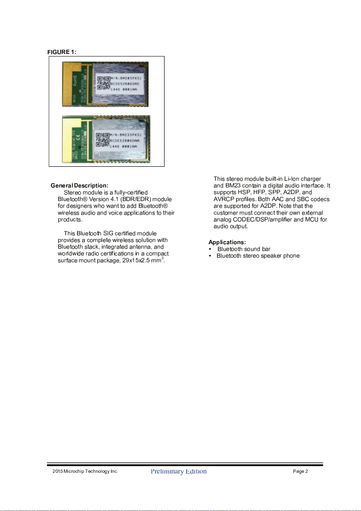
G
e ne ra l Desc ription
:
S
t
ereo module is a f
ully
Òc
ertified
B
lu
etoo
t
h
® V
ersion 4 .1 (
BDR/EDR)
module
for designers who wan
t t
o add
B
lu
etoo
t
h
®
wireless audio and voice applicationsto
t
h
eir
prod
u
c
t
s.
ThisB
lu
etoo
t
hSI
G
c
ertified module
provides acomplete wireless so
lu
t
ion wi
t
h
B
lu
etoo
t
h
sta
c
k,
integrated antenna,and
worldwide radiocertifications in acompa
c
t
surface mountpa
c
k
age
, 2 9x
1
5
x2
.5mm3.
Th
is stereo module bui
l
t
Ò
in L i
Ò
I
on
c
h
arger
and
BM23
c
ontain a digitalaudio interface.
I
t
supports H
SP
,
HF
P,SPP
, A 2DP,
and
AVR
CP
profiles.Bo
t
h AA
C
and
SBC
c
odecs
are supported for
A 2D
P
. N ote
t
h
a
t t
h
e
c
u
stomer mus
t
c
onne
c
t t
h
eir own e
x
t
erna
l
analog
CODEC/DSP/
amplifier and
M
CU
for
audio o
u
t
p
u
t
.
A
pplications
:
B
lu
etoo
t
h
sound bar
B
lu
etoo
t
h
stereo speaker phone
Page 3

201
5 M
icrochip Technol
ogy I
nc . P
ag
e 3
P
reliminar
y
Ed
ition
T
a
b le of Contents
1.0 D
E
V
I
CEO
V
E
RVIEW .................................................................................................................................. 4
2.0 A
PP
LICATIONINFO
RMATION............................................................................................................... 10
3.0
ELE
CTRICAL C
HA RA
CT
E
RISTICS ....................................................................................................... 18
4.0PRI
NT
E
D A
NTENN
A I
NFO
RMATION..................................................................................................... 23
5
.0 R
EFERENCE
CIRC
U
IT........................................................................................................................... 2
5
6
.0
C
E
RTIFICATIONI
NFO
RMATION..........................................................................................................2
7
7
.0 MOD
ULEOU
TLIN
E
AND R
EF
LO
WPR
O
F
I
L
E
...................................................................................... 29
8.0PACKA GING AND STORA GEI
NFO
RMATION....................................................................................34
A
PPE
N
DIX ........................................................................................................................................................ 3
7
T
O OU
R VALUED CUSTOMER
S
I
t
i
s
our
intention
t
opro
v
ide
ourva
luedcus
t
o
mer
s w
iththebe
stdoc
u
m
en
tat
ion possib
le
t
o
en
s
u
r
e
succe
ss
f
ulu
s
e
ofyour
M
icrochip products
. T
o
t
hisen
d , wew
ill continue
t
oimpro
v
e
our
pub
lic
a
t
ion
s
t
o
b
ettersui
t
your
needs.
O
u
r
pub
lic
a
t
ion
s
w
illberefine
dandenhance
dasnew
v
o
l
u
m
e
san
dup
d
a
t
e
sare in
t
ro
duced.
Ifyo
u
h
a
v
ean
y
q
u
e
stion
sorc
o
mm
entsre
gar
d
in
g
t
hispub
lic
a
t
ion,pleas
e con
t
a
c
t theM
ar
k
etin
gCo
mm
u
nic
a
t
ion
s
D
ep
artm
en
t
v
i
a
E%m
aila
t d
ocerrors@microch
ip
.
com
.Wewelc
o
meyour
f
ee
dback.
M
ost CurrentData
Sheet
T
o o
b
t
a
inthe
m
o
s
t
u
p
%
t
o
%
d
a
t
evers
ion
o
f
t
hi
s d
ata
s
heet,
pleas
eregi
ste
r atourWor
ldwideWe
b s
ite
a
t :
h
tt
p:
//
www
.
microch
ip
.
com
Y
o
u
candete
r
m
inethevers
ion
ofadata
s
heetbye
x
a
m
iningits
lite
ra
t
u
r
e n
u
m
b
e
rfo
u
n
donthe
b
ottomo
u
t
sid
e corne
r ofanypag
e .
The lastch
ara
cte
r o
f
t
he lite
ra
t
u
r
e n
u
m
b
eri
sthevers
ion n
u
m
b
er, (
e .g.
, DS30000000Ai
svers
ion
A
o
f
doc
u
m
entDS30000000).
E
rrata
A
n e
rrata
s
heet, des
cribin
g
minor opera
t
ionaldifference
s
f
ro
m
t
he
d
ata
s
hee
t
a
n
drec
o
mm
ende
d w
orkaro
u
n
ds ,
m
ay
exi
s
t
f
or
c
u
rr
entd
evices.
As d
evice
/doc
u
m
en
tat
ion i
ssue
s b
ec
o
mekno
w
n
t
o
u
s , wew
ill publis
han e
rrata
s
heet. The e
rrata
w
ill
s
peci
f
y
t
herevision
o
f
s
iliconan
drevision
o
f
doc
u
m
en
t t
o
w
hich i
t
a
pplies.
Tod
ete
r
m
ine i
f
a
n e
rrata
s
heetexi
sts
f
or apar
t
iculard
evice,pleas
e checkw
ithone
o
f
t
he
f
ollo
w
in
g
:
•
M
icrochip
’s WorldwideWe
b s
ite
;
h
tt
p:
//
www
.
microch
ip
.
com
•
Y
ourloca
lMicrochip
sale
s
o
ff
ice(see lastpage
)
W
hen con
t
a
ctin
g asa
le
s
o
ff
ice,pleases
peci
f
y
w
hichdevice
,revision
o
f
s
iliconan
d d
ata
s
heet(
includ
e lite
ra
t
u
r
e n
u
m
b
er)
youar
eus
ing.
Cust ome rNot ificat ionSyste m
R
egi
ste
r onour
web s
ite
a
t
www
.
microch
ip
.
comto r
eceivethe
m
o
stc
u
rr
entin
f
orma
t
iononall
ofourpro
ducts
.
A bbr
e
v iation
s
L
i
s
t :
HFP:Hands
a
f
ree Pr
o
f
il
e
AVRCP:Audi
o
V
i
de
o
R
emote
Contro
l
Pr
o
f
il
e
A
2DP:A
dvancedAud
ioDi
stribut
i
onPro
f
il
e
PBAP
: P
h
on
e
B
oo
k A
ccess Pr
o
f
il
e
H
SP:Headset Pr
o
f
il
e
SPP:SerialPort Pr
o
f
il
e
Page 4
201
5 M
icrochip Techn
ology I
nc . P
ag
e
4
P
rel
imi
nar
y
Ed
iti
on
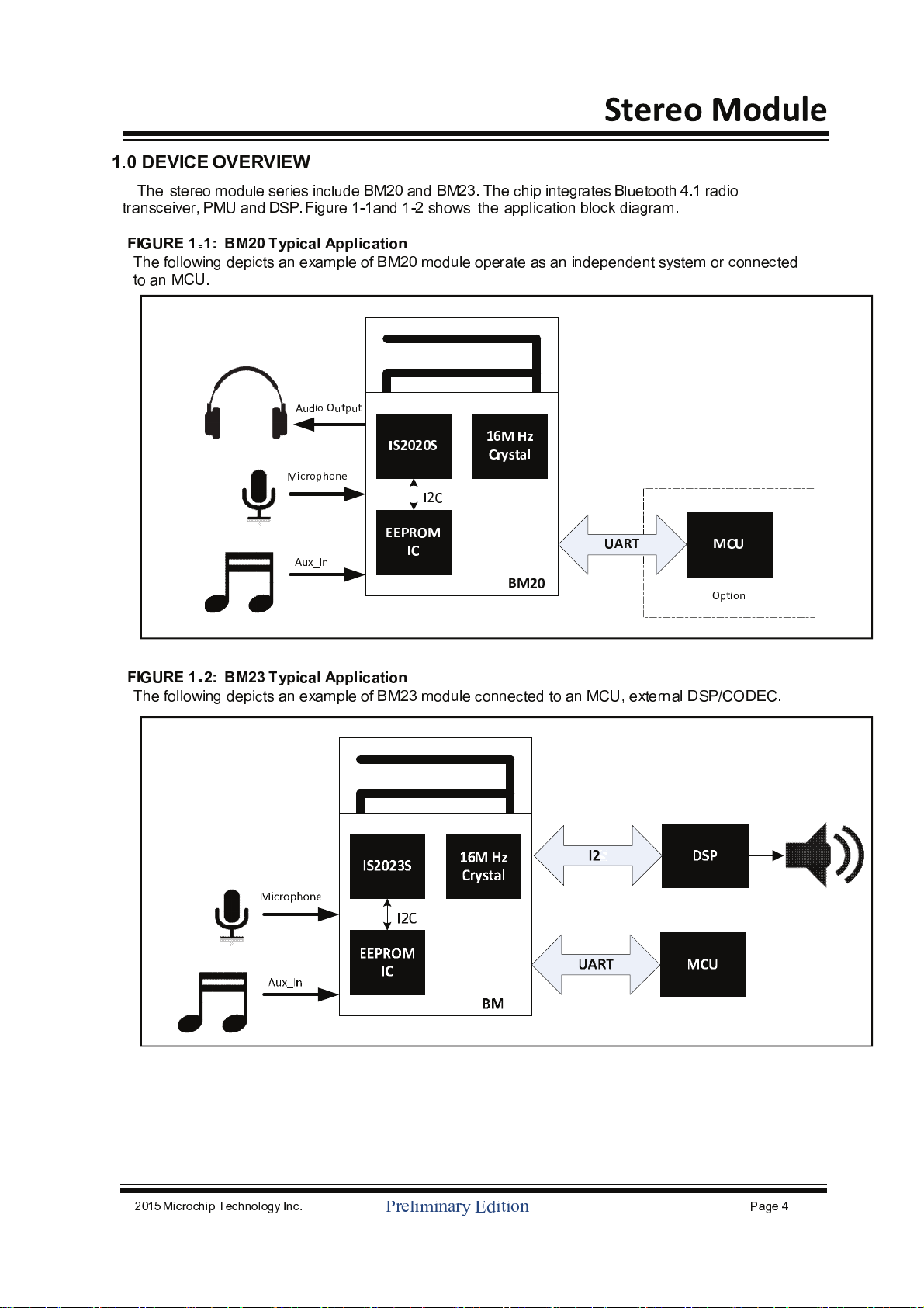
1
.0 D
EV ICE OVE RV IEW
Th
e stereo m odule series in
c
lu
de
BM2
0
and
BM23.Th
e
c
h
ip integrates
B
lu
etoo
t
h
4. 1 radio
t
ransceiver
,PM
U
and
D
SP
. Figure 1Ò1and 1
Ò
2sh
ows
t
h
e application blo
c
k
diagram.
FI
GURE 1®1:
BM
20 T y
pica lApplication
Th
e following dep i
c
t
s an example of
BM2
0
module operate as an independentsystem orconne
c
t
ed
t
o an
M
CU
.
FI
GURE 1
®
2
:
BM
23 T y
pica lApplication
Th
e following dep i
c
t
s an example of
BM23
moduleconne
c
tedt
o an
MCU,ex
t
erna
l
D
SP/ CODEC
.
ġ
ġ
M
C U
EEPROM
I
C
I
S2020S 1
6
M H
z
C r
ysta l
I2C
U
A RT
BM
20 O
ption
M
icrophone
Aux_I
n
Aud
io
O
utpu
t
Page 5
201
5 M
icrochip Technol
ogy I
nc . P
ag
e
5
P
reliminar
y
Ed
ition
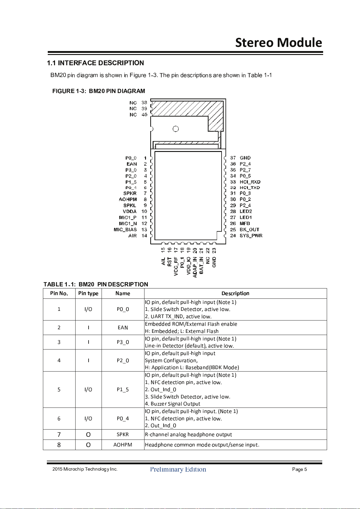
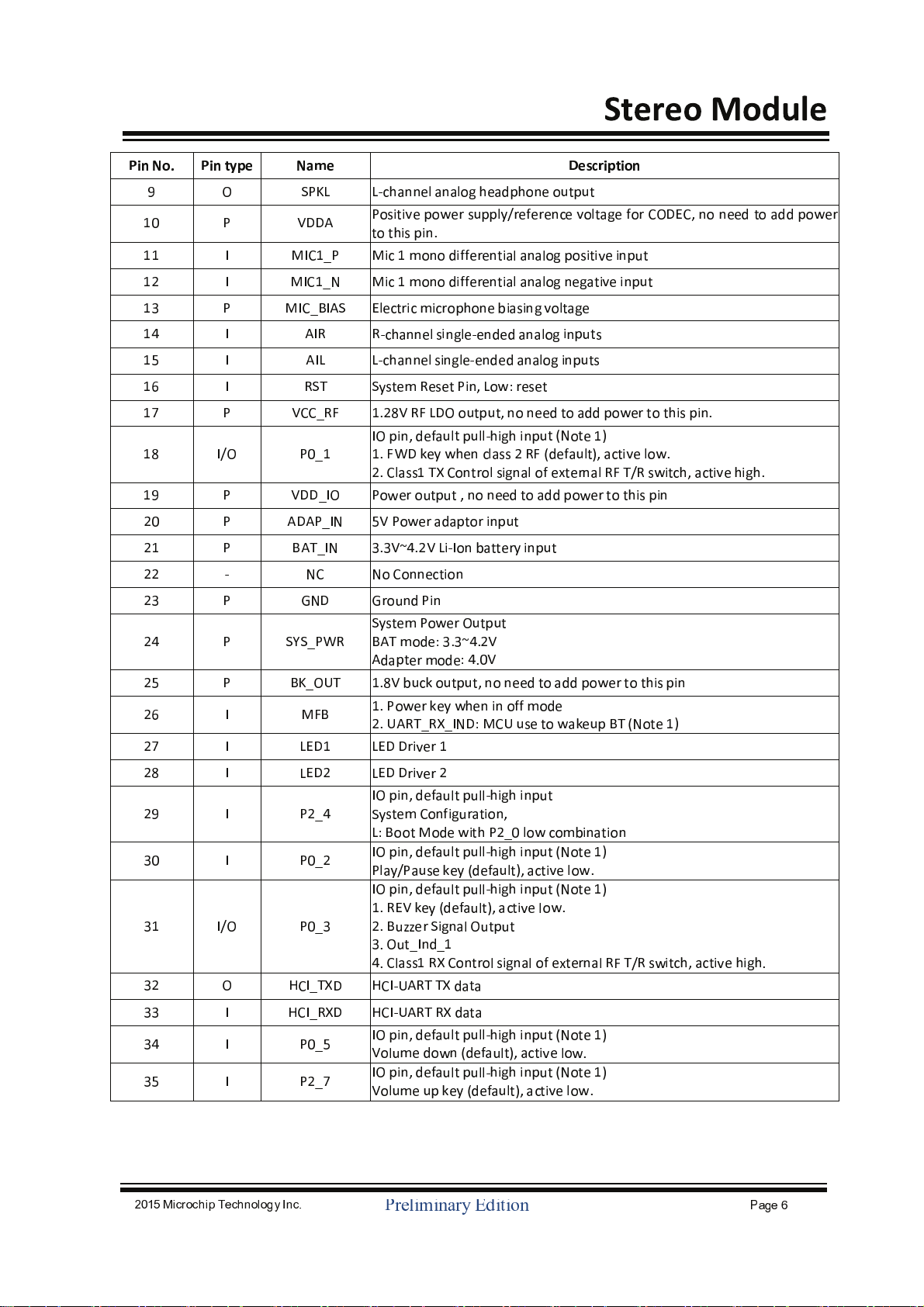
1.1 INT ERFAC E DESC RIPT ION
B
M20pi
n
diagramis s
h
ownin
Figure
1a3.Th
e p
i
n
descript
i
on
s are s
h
ownin T
able
1a1
F
I
GU
R
E 1Ç3
:
B
M20P
I
N D
I
AGRA M
T
A
B
L
E 1®1
:
B
M20P
I
N DES
CRI
P
T
ION
P
i n N
o .
P
i n t
y pe
N
a me Desc riptio
n
1 I/O P0_0
IO
pi
n
, defa
ul
t
p
ull
í
h
i
g
h
inp
u
t ( Not
e
1
)
1
. S
l
i
de
Sw
i
t
c
h D
etector, ac
t
i
vel
o
w.
2
. U
A RT TX_ I
N
D
, ac
t
i
vel
o
w.
2 I
E
A
N
E
mbedded
RO
M/E
x
t
erna
lFl
a
shena
b
l
e
H: E
mbedded
; L
: E
x
t
erna
lFl
a
s
h
3
I P3_0
IO
pi
n
, defa
ul
t
p
ull
í
h
i
g
h
inp
u
t
( Not
e
1
)
Line
í
i
nDetector(defa
ul
t
)
, ac
t
i
vel
o
w.
4
I P2_0
IO
pi
n
, defa
ul
t
p
ull
í
h
i
g
h
inp
u
t
S
y
ste
m C
on
f
i
gura
t
i
on,
H:
Appli
ca
t
i
on
L
: B
aseband
(
I
BDK M
ode
)
5
I/O P1_
5
IO
pi
n
, defa
ul
t
p
ull
í
h
i
g
h
inp
u
t ( Not
e
1
)
1
.
N
F
C
detec
t
ionpi
n, a c
t
i
vel
o
w.
2.O
u
t
_ Ind_0
3
. S
l
i
de
Sw
i
t
c
h D
etector, ac
t
i
vel
o
w.
4.B
u
zz
er
S
i
gna
lOu
t
p
u
t
6
I/O P0_
4
IO
pi
n
, defa
ul
t
p
ull
í
h
i
g
h
inp
u
t.( Not
e
1
)
1
.
N
F
C
detec
t
ionpi
n, a c
t
i
vel
o
w.
2.O
u
t
_ Ind_0
7 O
S
PKR R
í
channelanaloghead
p
h
one o
u
t
p
u
t
8
O
AOHP
M H
ead
p
h
one commonmode o
u
t
p
u
t
/
sens
ein
p
u
t
.
Page 6
201
5 M
icrochip Technol
ogy I
nc . P
ag
e
6
P
reliminar
y
Ed
ition
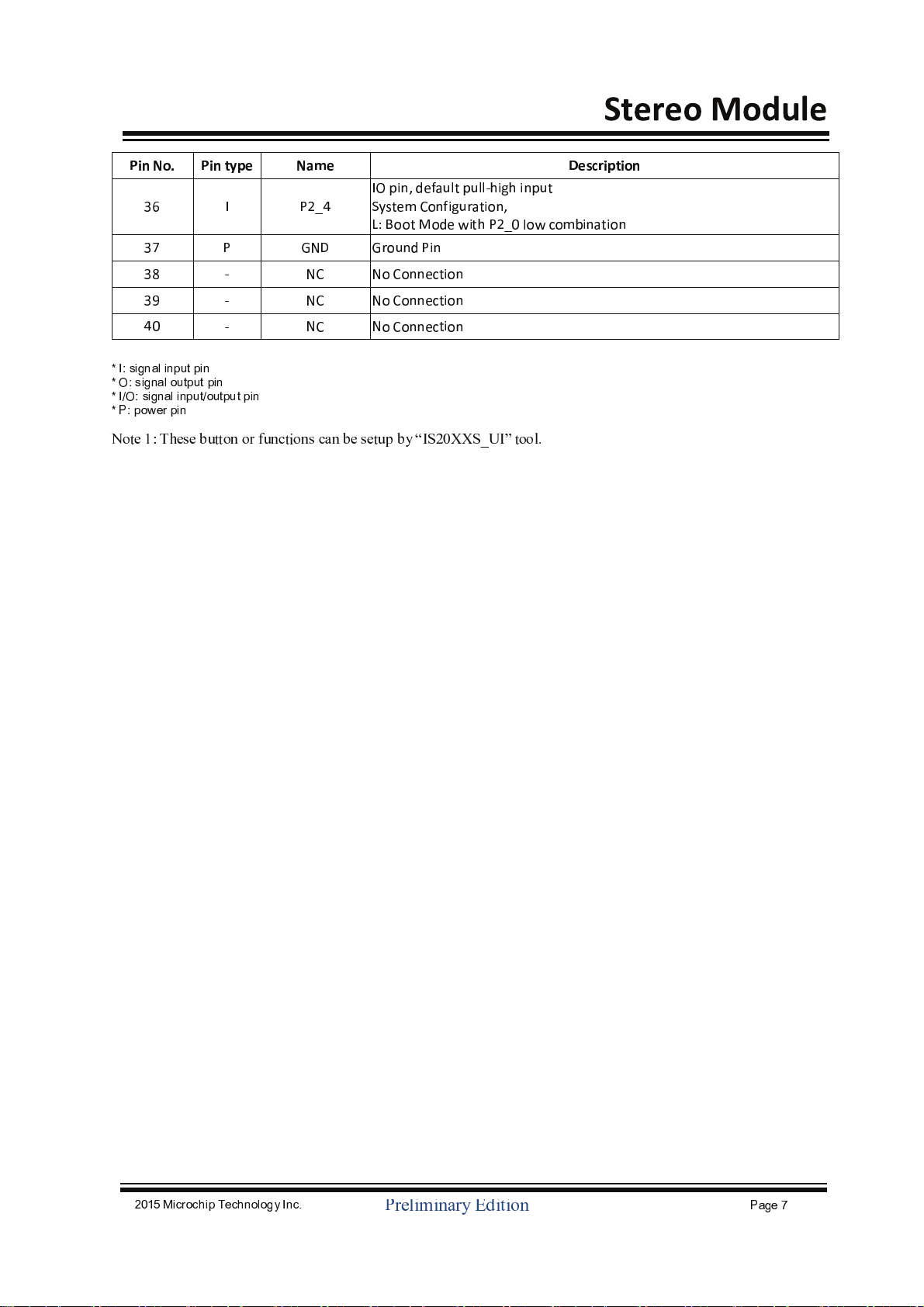
P
i n N
o .
P
i n t
y pe
N
a me Desc riptio
n
9
O
S
P
K
L Líchannelanaloghead
p
h
one o
u
t
p
u
t
10 P
VDDA
P
o
s
iti
v
epower
s
uppl
y
/
referencevo
l
t
agefor
C
ODE
C
, no n eedto addpower
tot
h
ispi
n
.
11 I
M
IC1_ P
M
ic1
m
ono d
i
ff
eren
t
i
alanalogpo
s
iti
v
ein
p
u
t
12 I
M
IC1_
N
M
ic1
m
ono d
i
ff
eren
t
i
alanalog nega
t
i
v
ein
p
u
t
1
3
P
M
IC_BIA
S
E
l
ectric
micro
p
h
one
b
i
a
singvo
l
t
age
1
4
I A IR R
í
channelsingleíended analogin
p
u
t
s
1
5
I A I
L Líchannelsingleíended analogin
p
u
t
s
1
6
I RST
S
y
ste
mRese
t
Pi
n,Lo
w
:
rese
t
1
7
P
VCC_R
F
1.28VR
F
L
D
O
o
u
t
p
u
t
, no needto addpowerto
t
h
ispi
n
.
1
8
I/O P0_ 1
IO
pi
n
, defa
ul
t
p
ull
í
h
i
g
h
inp
u
t ( Not
e
1
)
1
.
F
W
D
k
e
y
w
h
en cla
ss
2 R
F
(
defa
ul
t
)
, ac
t
i
vel
o
w.
2
.
Cla
ss
1 T
X
C
ontrolsignalofe
x
t
erna
lRF
T/R
s
w
i
t
ch, ac
t
i
v
e
h
i
g
h
.
1
9
P
VDD_ IO P
ower o
u
t
p
u
t
, no needto addpowerto
t
h
ispi
n
20 P ADA P_ I
N
5V
P
ower ada
p
t
orin
p
u
t
2 1 P
B
AT_ I
N
3.3V~4.2
VLiíI
onbatter
y
inp
u
t
22
í
N
C
N
oConnec
t
i
on
2
3
P
G
N
D
G
roundPin
2
4
P
SYS
_ PWR
S
y
ste
mPower
O
u
t
p
u
t
B
AT
m
ode
: 3.3~4.2
V
Adap
t
ermode
: 4.0
V
2
5
P
BK
_OUT 1.8V
b
u
cko
u
t
p
u
t
, no needto addpowerto
t
h
ispi
n
2
6
I
MFB
1.P
owerke
y
w
h
enin offm
ode
2
. U
A RT_ RX_ I
N
D
: M
C
U
u
s
etowake
u
pBT
(Not
e
1
)
2
7
I
L
ED1
L
E
D D
r
i
v
er
1
2
8
I
L
ED2
L
E
D D
r
i
v
er
2
2
9
I P2_
4
IO
pi
n
, defa
ul
t
p
ull
í
h
i
g
h
inp
u
t
S
y
ste
m C
on
f
i
gura
t
i
on,
L
: B
oo
t
M
ode
w
i
t
h
P2_0
l
owco
m
b
i
na
t
i
on
3
0 I P0_2
IO
pi
n
, defa
ul
t
p
ull
í
h
i
g
h
inp
u
t
( Not
e
1
)
P
lay
/
P
aus
eke
y
(
defa
ul
t
)
, ac
t
i
vel
o
w.
3
1 I/O P0_
3
IO
pi
n
, defa
ul
t
p
ull
í
h
i
g
h
inp
u
t ( Not
e
1
)
1.R
EV
k
e
y
(
defa
ul
t
)
, ac
t
i
vel
o
w.
2.B
u
zz
er
S
i
gna
lOu
t
p
u
t
3.O
u
t
_ Ind_1
4
.
Cla
ss
1 R
X
C
ontrolsignalofe
x
t
erna
lRF
T/R
s
w
i
t
ch, ac
t
i
v
e
h
i
g
h
.
3
2 O
HCI_T
X
D
HCI
í
U
A RT T
X
data
33
I
HCI_ R
X
D
HCI
í
U
A RT R
X
data
34
I P0_
5
IO
pi
n
, defa
ul
t
p
ull
í
h
i
g
h
inp
u
t
( Not
e
1
)
V
olum
e down(defa
ul
t
)
, ac
t
i
vel
o
w.
35
I P2_
7
IO
pi
n
, defa
ul
t
p
ull
í
h
i
g
h
inp
u
t
( Not
e
1
)
V
olum
e
u
p
k
e
y
(
defa
ul
t
)
, ac
t
i
vel
o
w.
Page 7
201
5 M
icrochip Technol
ogy I
nc . P
ag
e
7
P
reliminar
y
Ed
ition
P
i n N
o .
P
i n t
y pe
N
a me Desc riptio
n
36
I P2_
4
IO
pi
n
, defa
ul
t
p
ull
í
h
i
g
h
inp
u
t
S
y
ste
m C
on
f
i
gura
t
i
on,
L
: B
oo
t
M
ode
w
i
t
h
P2_0
l
owco
m
b
i
na
t
i
on
37
P
G
N
D
G
roundPin
38
í
N
C
N
oConnec
t
i
on
39
í
N
C
N
oConnec
t
i
on
4
0
í
N
C
N
oConnec
t
i
on
*
I
: signa
l inputpin
* O
: signalo
utput
pin
*I/O
: signa
l inp
ut
/
o
utput
pin
*
P
:po
w
erpin
N o
t
e 1: T heseb u
tt
onor f
u nc
t
i
o
ns can b e setup by “I
S20XXS
_
U
I
”
t
ool
.
Page 8
201
5 M
icrochip Technol
ogy I
nc . P
ag
e
8
P
reliminar
y
Ed
ition
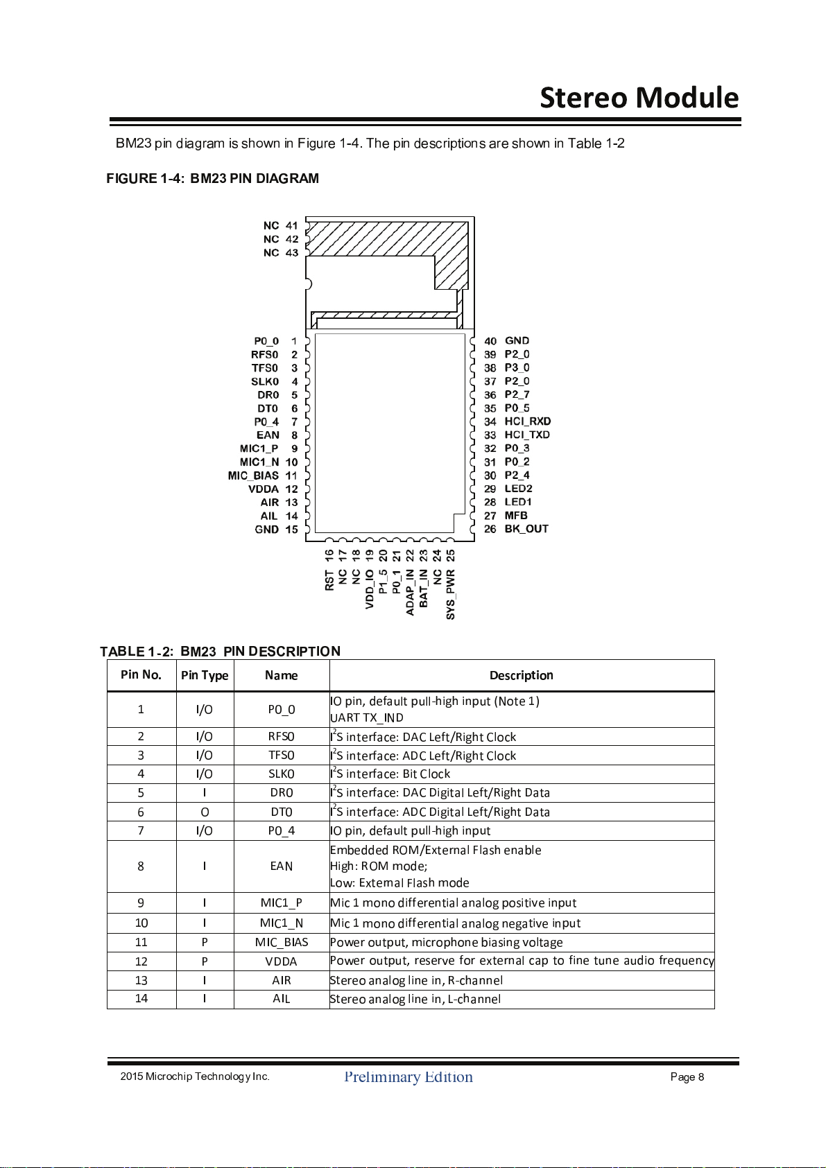
B
M23pi
n
diagramis s
h
ownin
Figure
1a4.Th
e p
i
n
descript
i
on
s are s
h
ownin T
able
1a2
F
I
GU
R
E 1Ç
4
:
B
M23P
I
N D
I
AGRA M
T
A
B
L
E 1®2
:
B
M23P
I
N DES
CRI
P
T
ION
P
i n N
o .
P
i n
T
y pe
N
a me Desc riptio
n
1 I/O P0_0
IO pi
n, defa
ul
t
p
ull
í
h
i
g
h
inp
u
t ( Not
e
1
)
U
A RT TX_ I
N
D
2 I/O R
F
S
0
I
2
S
i
nterface
:DA
C L
e
f
t
/
Ri
g
h
t
Cloc
k
3
I/O T
F
S
0
I
2
S
i
nterface
:
A
D
C L
e
f
t
/
Ri
g
h
t
Cloc
k
4
I/O
S
L
K
0 I
2
S
i
nterface
: B
i
t
Cloc
k
5
I
D
R0 I
2
S
i
nterface
:DA
C
D
igi
t
alL
e
f
t
/
Ri
g
htD
ata
6
O
D
T0 I
2
S
i
nterface
:
A
DCD
igi
t
alL
e
f
t
/
Ri
g
htD
ata
7
I/O P0_
4
IO pi
n, defa
ul
t
p
ull
í
h
i
g
h
inp
u
t
8
I
E
A
N
E
mbedded
RO
M/E
x
t
erna
lFl
a
shena
b
l
e
H
i
g
h
:ROM
m
ode
;
L
o
w
: E
x
t
erna
lFl
a
shm
ode
9
I
M
IC1_ P
M
ic1
m
ono d
i
ff
eren
t
i
alanalogpo
s
iti
v
ein
p
u
t
10 I
M
IC1_
N
M
ic1
m
ono d
i
ff
eren
t
i
alanalog nega
t
i
v
ein
p
u
t
11 P
M
IC_BIA
S
P
ower o
u
t
p
u
t
,
micro
p
h
one
b
i
a
singvo
l
t
age
12 P
VDDA
P
ower o
u
t
p
u
t
, reservefor e
x
t
ernalca
p
t
o
f
i
ne
t
u
ne audiofre
quenc
y
1
3
I A IR
S
t
ereo analog
l
inein,R
í
channe
l
1
4
I A I
L
S
t
ereo analog
l
inei
n,
Líchanne
l
Page 9
201
5 M
icrochip Technol
ogy I
nc . P
ag
e
9
P
reliminar
y
Ed
ition
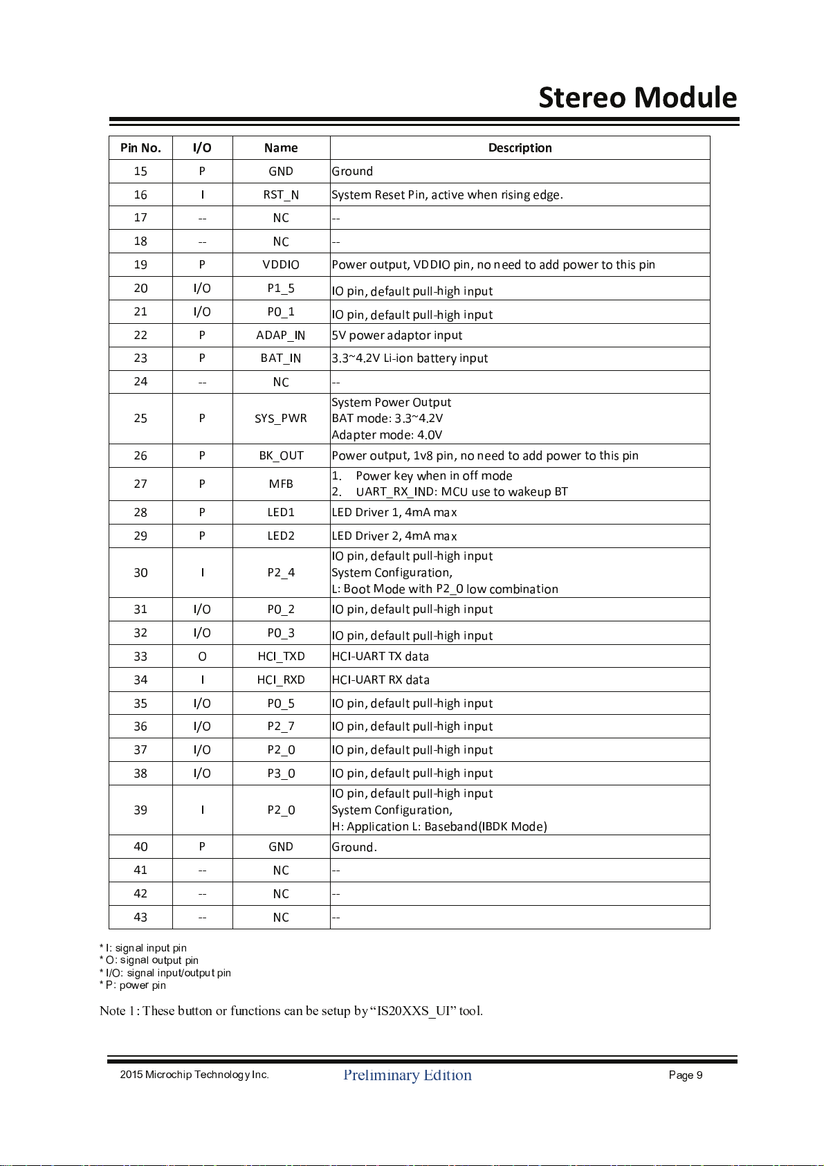
P
i n N
o .
I
/
O
N
a me Descriptio
n
1
5
P
G
N
D
G
round
1
6
I RST_
N
S
y
ste
mRese
t
Pi
n, a c
t
i
v
e
w
h
en rising edge
.
1
7
íí
N
C
íí
1
8
íí
N
C
íí
1
9
P
VDDIO P
ower o
u
t
p
u
t
,
VDDIO pi
n, no needto addpowerto
t
h
ispi
n
20 I/O P1_
5
IO p i
n, defa
ul
t
p
ull
í
h
i
g
h
inp
u
t
2 1 I/O P0_ 1
IO p i
n, defa
ul
t
p
ull
í
h
i
g
h
inp
u
t
22 P ADA P_ I
N
5V
p
ower ada
p
t
orin
p
u
t
2
3
P
B
AT_ I
N
3.3~4.2
VLiíi
onbatter
y
inp
u
t
2
4
íí
N
C
íí
2
5
P
SYS
_ PWR
S
y
ste
mPower
O
u
t
p
u
t
B
AT
m
ode
: 3.3~4.2
V
Adap
t
ermode
: 4.0
V
2
6
P
BK
_OUT P
ower o
u
t
p
u
t
,
1v8
pi
n, no needto addpowerto
t
h
ispi
n
2
7
P
MFB
1.P
owerke
y
w
h
enin offm
ode
2
. U
A RT_ RX_ I
N
D
: M
C
U
u
s
etowake
u
pBT
2
8
P
L
ED1
L
E
D D
r
i
v
er1,4mAm
a
x
2
9
P
L
ED2
L
E
D D
r
i
v
er2,4mAm
a
x
3
0 I P2_
4
IO
pi
n
, defa
ul
t
p
ull
í
h
i
g
h
inp
u
t
S
y
ste
m C
on
f
i
gura
t
i
on,
L
: B
oo
t
M
ode
w
i
t
h
P2_0
l
owco
m
b
i
na
t
i
on
3
1 I/O P0_2 IO pi
n, defa
ul
t
p
ull
í
h
i
g
h
inp
u
t
3
2 I/O P0_
3
IO p i
n, defa
ul
t
p
ull
í
h
i
g
h
inp
u
t
33
O
HCI_T
X
D
HCI
í
U
A RT T
X
data
34
I
HCI_ R
X
D
HCI
í
U
A RT R
X
data
35
I/O P0_
5
IO p i
n, defa
ul
t
p
ull
í
h
i
g
h
inp
u
t
36
I/O P2_
7
IO p i
n, defa
ul
t
p
ull
í
h
i
g
h
inp
u
t
37
I/O P2_0 IO pi
n, defa
ul
t
p
ull
í
h
i
g
h
inp
u
t
38
I/O P3_0 IO p i
n, defa
ul
t
p
ull
í
h
i
g
h
inp
u
t
39
I P2_0
IO
pi
n
, defa
ul
t
p
ull
í
h
i
g
h
inp
u
t
S
y
ste
m C
on
f
i
gura
t
i
on,
H:
Appli
ca
t
i
on
L
: B
aseband
(
I
BDK M
ode
)
4
0 P
G
N
D
G
round
.
4
1
íí
N
C
íí
4
2
íí
N
C
íí
43
íí
N
C
íí
*
I
: signa
l inputpin
* O
: signalo
utput
pin
*I/O
: signa
l inp
ut
/
o
utput
pin
*
P
:po
w
erpin
N o
t
e 1: T heseb u
tt
onor f
u nc
t
i
o
ns can b e setup by “I
S20XXS
_
U
I
”
t
ool
.
Page 10
201
5 M
icrochip Techn
ology I
nc . P
ag
e
10
P
rel
imi
nar
y
Ed
iti
on
2
.0
A PPL
I
C
A T
IONINFOR
M
A T
IO
N
2 .1 O PERAT IO N WIT H EXT ERNA L M
C U
S
t
ereo module suppor
t
U
ART
c
ommand se
t t
o make an e
x
t
erna
l
M
CU
t
ocontrolmodule.
Here is
t
h
econne
c
t
ion interface between
BM
XX
and
M
CU
.
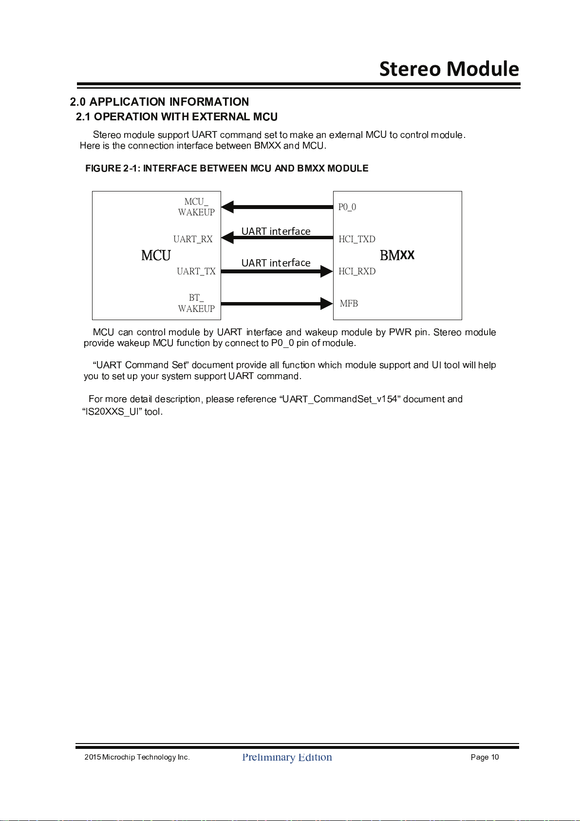
FI
GURE
2
m1:INTERFA
C
EBE
T
WEENMCUA
N
D
BMXXM
ODULE
M
CU
canc
ontrolmodule b
y
U
ART
interface and wakeup module b
y
P
W
R
pin.
S
t
ereo m odule
provide wakeup
M
CU
fun
c
t
ion b
y
c
onne
c
t t
o
P
0_0
pin of module.
“UART
C
ommandSe
t
”
do
c
u
mentprovide allfun
c
t
ion whi
c
h
module supportand
U
I
t
oolwi
ll
h
elp
you
t
o se
t
upyou
r system suppor
t
U
A RT
c
ommand.
For more detaildescription,please reference
“UAR T
_
C
ommandSe
t
_
v154”do
c
u
mentand
“
IS20XX
S_U
I
”
t
ool.
XX
ʼnńŊŠŕřŅ
ʼnńŊŠœřŅ
ŎŇŃ
őıŠı
ŖłœŕŠŕř
ŖłœŕŠœř
ŎńŖŠ
ŘłŌņŖő
ŃŕŠ
ŘłŌņŖő
UA RT i n
te r
fa
c
e
UA RT i n
te r
fa
c
e
Page 11
201
5 M
icrochip Techn
ology I
nc . P
ag
e
11
P
rel
imi
nar
y
Ed
iti
on
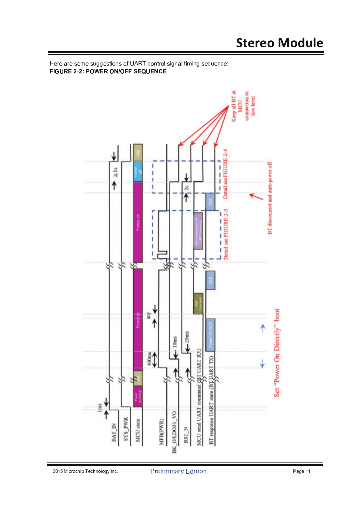
Here are some suggestions of
U
ART
c
ontrolsigna
l
t
iming se
quence
:
FI
GURE
2m2
:
POWER
ON/O
FF
S
EQUENCE
Page 12

201
5 M
icrochip Techn
ology I
nc . P
ag
e
12
P
rel
imi
nar
y
Ed
iti
on
FI
GU R
E 23 :
T
IMI
NGS
EQUENCE
OFR
XINDICATIONAFT
ER
POWER
O
N
FI
GU R
E 24 :
T
IMI
NGS
EQUENCE
OFPOWER
O
FF
Page 13

201
5 M
icrochip Techn
ology I
nc . P
ag
e13
P
rel
imi
nar
y
Ed
iti
on
FI
GURE
2
m
5
:
T
IMI
NGS
EQUENCE
OFPOWER
O
N (NACK
)
FI
GURE
2
m6
: RESE
T T
IMI
NGS
EQUENCEIFM
ODULE
H
A
NGS
U
P
Page 14
201
5 M
icrochip Technol
ogy I
nc . P
ag
e14
P
reliminar
y
Ed
ition
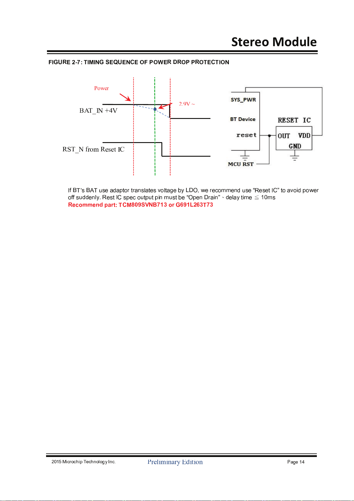
FI
GUR
E 2 ¥
7 : T
IMIN
G SEQUENC
E OF POW E
R DR
OP PROTE
C
T
ION
BAT
_ I
N +4V
ġ
RST_N f
romReset
I
C
ġ
I
f
B
T’
s
B
AT u
se adaptor translates voltage by LD
O, w
e recommen
d u
se “Reset
I
C”
to avoidpower
offs
uddenl
y
.
R
est
I
C
spec output p in must be “Open Drain
”
ˣ
del
ay time
ʀ
1
0
ms
R
ec omme n
d p
a r
t : T C M
809SVNB
7
1
3
or
G
6
91L263
T
7
3
Pow
er
2.9
V ~
Page 15

201
5 M
icrochip Techn
ology I
nc . P
ag
e
1
5
P
rel
imi
nar
y
Ed
iti
on
2 .2 I
2
S S i
g na l
A
pp
licatio n for B
M2
3
BM23
suppor
t
I
2
S
digitalaudio signalinterfacetoconne
c
t
you
r e
x
t
erna
l
CODEC/DSP
.
I
t
provide
8
k
H
z
,
44. 1kHzand 4
8kHzsampling rate;italso support16bits and24bits data format.The
I
2
S
setting
c
an be se
t
u
p b
y
U
I
and
D
SP
t
ools.
.
Th
e e
x
t
erna
l
CODEC/DSP
needsto beconne
c
tedt
oSL
K
0
, R
F
S
0
, T
F
S
0
, DR0,
and
DT
0
(pins 4
, 2 , 3 ,
5
,
and6respe
c
t
ive
ly
).TheI
2
S
signa
l
c
onne
c
t
ion between
BM23
and e
x
t
erna
l
D
SP
as below
:
FI
GURE
2m9
:
M
AST
ERMODE REFERENCECONNE
CTION
FI
GURE
2
m10:SLA
V
EMODE REFERENCECONNE
CTION
N
ote 1 : For 00
2 v
ersion c hip or mo
dul
e , system sho
uld
connectline 1 in slave mode figure .
And
, system no t support
A D
C
signalfrom externa
l D
S P/CODEC
.
N
ote2: For otherversion c hip or mo
dul
e , system sho
uld
connectline2in slave mode figure .
A
bo
u
t
“
M
as
t
”or“
S
l
ave”mode setting
,
you
c
anuse
“
D
SP C
onfigurationToo
l
”
t
o se
t
u
p system.
Page 16

201
5 M
icrochip Techn
ology I
nc . P
ag
e16
P
rel
imi
nar
y
Ed
iti
on
Th
e cloc
k and data timingas b
elow
:
FI
GURE 2
11: T IMINGFORI
2
S
MOD
ES ( b
o
th mast
e r a nd s lave)
FI
GU R
E 212 :
T IMINGFO
R PC
M MOD
ES ( b
o
th mast
e r a nd s lave)
2 .3RESET(RS
T_ N
)
RST ismodu
le rese
t p i
n whic
h is acti
v
e LO
W. T
o rese
t th
e module
,
theRST
_ N
m
ust holdLOW forat
le
ast 63ns.
2 .4S
TAT
US LED(LE
D1,LED
2)
ThestatusLED p
ro
v
ideb
elow
status indicati
on
:
S
tandby
I
nquir
y
Lin
k
Lin
k Back
Low
Battery
P
a
ge
Battery C hargi
ng
Eac
h status indicati
on LE
D flashingsequ
encean
d brightness is
configurable
by UIt
ool
.
Page 17

201
5 M
icrochip Technol
ogy I
nc . P
ag
e17
P
reliminar
y
Ed
ition
2
.5EXT ERNALCONFI
G U
RAT ION
S
t
ereo mo
d
ul
e can be conf iguredandfirmware programme
d
us
ing an externalconfiguration an
d
programmingtoolavailable from Microchip. F igure 2
®
7
s
how
s
t
he configuration andfirmware
programming interface on BM23. Itisrecommende
d
t
o inc
lu
d
e a pin header onthe main PCB for
d
evelopment.
Configuration andfirmware p rogramm ing modesare enteredaccording
ly
tot
he
sys
t
em
configuration I
/ O
pinsa
s s
hown in Table 2î 1. Pin P20 , P24 and E
A N pi
n have internalp
ull®u
p.
FI
GUR
E 2 ¥
13:E
XTERNALPROGRA
MMIN
G
H
E
ADE
R C
ONNE
C
T
ION
S
(H
ere i
s
t
he interface connectexample ofthe BM23
)
T
ABL
E 2 ¥
1
:
SYS
T
EMCONFI
GUR
ATIONSETTIN
GS
P2
0
P2
4
EAN O
p
e rat iona lMode
H
igh
H
igh
H
igh
A
PP mode(Normaloperation
)
L
ow
H
igh
H
igh
Te
s
t
mode
(WriteEEP
R
O
M
)
L
ow
L
ow
H
igh
W
rite Flash(Firmware p rogramming if flash bui
l
d
îin in ch ip
)
Page 18

201
5 M
icrochip Technol
ogy I
nc . P
ag
e18
P
reliminar
y
Ed
ition
3
.0 ELEC
TRICA LCHA RACTERISTI
CS
Ta bl
e 3 .1
: A B
S OL
UT E MAX IMUM
S PEC
IFI
C
A
T I
ON
Symb
o l
Parameter
M in
Max
Un it
BAT_ IN I
npu
t vo lt
age f
o r batter
y 0 4 .3 V
A DA P_ IN I
npu
t vo lt
age f
o r
ada p
to r
0 7.0 V
T
S
TO RE
S
to r
agete mperature s6 5 +15
0 ºC
T
OPERAT ION
O
pera
t iont
e mperature s2
0
+
70 º C
Ta bl
e 3 .
2
: R
ECOMMENDE
D OP
ERAT I
NG COND
IT I
ON
Symb
o l
Parameter
M in
Typ ica l
Max
Un it
BAT_ IN I
npu
t vo lt
age f
o r batter
y 3 3.7 4.
2
V
A DA P_ IN I
npu
t vo lt
age f
o r
ada p
to r
4 .
5 5 5.5
V
T
OPERAT ION
O
pera
t iont
e mperature s2
0
+2 5 +
70 º C
N
ote :
Abs
olute and Recommended operating condition tablesreflect typical
u
s
agefor d e
v
i
ce .
TA B
LE 3¥3 : I
/O
AN
D RESETLEVE L
Parameter M in . Typ . Max . Un its
I
/
O
S
u
pp
l
y
V
o lt
age
(
V
DD_ I
O)
2
.7 3.0 3.3
V
I/OV
o ltageLeve ls
V
I
L
i
npu
t logiclevelslo
w
®
0.3 0.8 V
V
I
H
i
npu
t logiclevel
s hig h 2
.0 3.
6
V
V
O
L
output logiclevelslo
w 0.4 V
V
O
H
output logiclevel
s hig h 2
.4 V
RESE
T
V
,
RE
S
thr
esh
o ldvo lt
age 1.6
V
N
ote :
( 1) V DD
_ I
O
v
oltageisprogrammableby EEPR
O
M
parameters.
(2) Th
ese p arametersare character
i
z
ed
b
u
t not testedin man
u
f
acturing .
Page 19

201
5 M
icrochip Technol
ogy I
nc . P
ag
e19
P
reliminar
y
Ed
ition
Ta bl
e 3 ð
4
: BA
TT ERYCH
AR
G
E
R
Parameter
y
p ica l
A DA P_ IN I
npu
tVo lt
age
4 .
5 5
.0
5.5
V
S
upp
l
y
curre n
t to
charge
r onl
y 3 4.
5 m
A
M
aximumBatte
r
y
F
as
t
C
hargeCurre n
t
N
ot
e : ENX2 =
0
Head
roo
m >
0.7V
(
A DA P_IN
=5
V
)
1
70
2
00
2
4 0
m
A
Head
roo
m =
0.3V
(
A DA P_IN
=
4 .5V
)
16
0
1
80
2
4 0
m
A
M
aximumBatte
r
y
F
as
t
C
hargeCurre n
t
N
ot
e : ENX2 =1
Head
roo
m >
0.7V
(
A DA P_IN
=5
V
)
330 350 420
m
A
Head
roo
m =
0.3V
(
A DA P_IN
=
4 .5V
)
1
80
22
0
2
70
m
A
T
rickl
eCharge
V
o lt
ageThres h
o l
d
3 V
B
atte
r
y C
hargeTermina
t io
nCurre n
t ,
(
%
o
fFas
t
C
hargeCurre n
t
)
1
0
%
N
ote :
( 1) H
eadroom
=
V
ADA
P
_IN –
V
BA
T
(2)
E
NX2 is
not allowed tobe enabled
when
V
ADA
P
_IN –
V
BA
T >
2
V
(3) Th
ese parametersare character
i
z
ed
b
u
t not testedin man
u
f
acturing .
Ta bl
e 3 .
5
:
LED D
R
IVE
R
Para
mete
r
M
in
T
y p
ical
M
a
x
U
ni
t
Op
en
#
dr
ain Voltage 3 .
6
V
Progr
ammable C
u
rr
en
t R
ange 0 5 .25 m
A
I
ntensityCon
t
r
ol 1
6
ste
p
C
u
rr
en
t St
e
p
0 .35 m
A
P
owe
r D
ownOpen
#
dr
ain C
u
rr
en
t
1
ȫ
A
Shut
d
own C
u
rr
en
t
1
ȫ
A
N
ote :
( 1) T
est condition :
SAR
_
V DD=1
.
8
V
,
temperature
=
2
5 º
C
.
(2) Th
ese parametersare character
i
z
ed
b
u
t not testedin man
u
f
acturing .
Page 20

201
5 M
icrochip Technol
ogy I
nc . P
ag
e
20
P
reliminar
y
Ed
ition
Ta bl
e 3 .
6
: A
UDI
O CODECANALOG
UE T
O DIG
IT
A
L CON
V
ERT E
R
T
= 2 5
o
C,V
dd=3.0V
,
1
K
H
z
sinewaveinpu
t ,
B
a n
d
w
idt
h = 2
0Hz
~
20K
H
z
m
eter
(Condit ion
)
y
p .
R
es
o lut io
n 16
B
it
s
O
utpu
t
S
a mpleRate
8 48
K
H
z
S
i
g na
l toNo i
seRa
t io
Note
:
1
(
S
N
R @
MI
C
o rLi
nesin m
o
d
e
)
88
d B
D
igital
Gai
n s 5
4 4 .8
5
d B
D
igital
Gai
nRes
o lut io
n 2~6
d B
MICB
oost
Gai
n 2
0
d B
A
nalogGain 6
0
d B
A
nalogGainRes
o lut io
n 2
.0
d B
I
nputf ullsscale atmaximum gain (
d
i
ffere n
t ial
)
4
m
V
r
ms
I
nputf ullsscale atminimum gain (
d
i
ffere n
t ial
)
800
m
V
r
ms
3
d B
b
a n
d
w
idt
h 2
0
K
H
z
M
icropho
ne m
o
d
e (inpu
t i
mpeda nce
)
2
4
KV
+N(microphoneinpu
t
)
@
30mV
rmsi
npu
t
0.0
2
%
N
ote :
( 1)
f
i
n
=
1KHz, B/
W=20~2
0K
Hz,
A
b
w
eighted
,
T HD
+
N
<
1
% ,
1
50
m
V
pp
i
nput
(2)
Th
ese parametersare character
i
z
ed
b
u
t not testedin man
u
f
acturing .
Page 21

201
5 M
icrochip Technol
ogy I
nc . P
ag
e
2 1
P
reliminar
y
Ed
ition
Ta bl
e 3 .
7
: A
UDI
O CODEC DIG
IT
A
LTOANALOGUECON
V
ERT E
R
5
dd
3 .0V , 1
KH
z
sine wave in
p
u
t
, Bandwi
dth= 2
0
Hz20KH
z
Para
mete
r
(
C
o
ndition
)Min.
T
y p
.Max.Uni
t
v
e
r
p
lingrate
1
28
f
R
esol
u
t
ion
160
Bits
u
t
p
u
t S
ampleRate
KH
z
ignalto NoiseRatio
N
o
te: 1
(
SNR @
ca
p
#
less mode) fo
r 48k H
z 9
6 d
B
ignalto NoiseRatio
N
o
te: 1
(
SNR @
single#endmode) fo
r 48k H
z 9
8 d
B
D
igital Gain
#
5
4 4.8
5
d
B
D
igital GainResol
u
t
ion
2~6 d
B
A
nalog Gain
#
28
3
d
B
nalog GainResol
u
t
ion
1
d
B
O
u
t
p
u
t
Voltage Full#scaleSwing
(
AVDD=2.8
V)
4
9
5 742.5
mVrm
s
M
aximum
O
u
t
p
u
t
P
owe
r
1
6d
34.5
W
M
aximum
O
u
t
p
u
t
P
owe
r
2d
17 .
2
W
A
llowe
d Load
R
esistive
8
1
6
O
.C .
ȟ
p
acitive
500
űŇġ
+
N
1
6ȟd
0 .05 %
S
ignalto NoiseRatio
(
SNR @
1
6
ȟ
load)
9
6 d
B
N
ote :
( 1) f
i
n
=
1KHz, B/
W=20~2
0K
Hz,
A
b
w
eighted
,
T HD
+
N
< 0.0
1
% ,
0
d
B F
Ssignal
, L
oad
=
1
00K
(2) Th
ese parametersare character
i
z
ed
b
u
t not testedin man
u
f
acturing .
Ta bl
e 3 .
8:T
RA
NS
MITT E
R
SEC
T IONF
O
R BDR A
NDED
R
Para
mete
r
M
in
T
y p
M
a
x
B
lu
etoo
t h
spe
cification
U
ni
t
M
aximumRF
t
r
ansmi
t
p
owe
r
3 .0
4
.0
#
6
t
o
4 d
Bm
ED
R
/
B
D
R
R
elative
t
r
ansmi
t
p
owe
r
#
4
#
1.
2
1
#
4
t
o 1
d
B
N
ote :
Th
e R
F
T
ransmit poweriscalibrated during p roduction
u
singM P
T
oolsoftware and
MT885
2
B
luetoot
h T
est
e
q
u
i
pment .
T
est condition :
V
CC
_
RF=1.
2
8
V
,
temperature
=
2
5 º
C
.
Page 22

201
5 M
icrochip Technol
ogy I
nc . P
ag
e
22
P
reliminar
y
Ed
ition
Ta bl
e 3 .
9
: R
ECEIVE
R
SEC
T IONF
O
R BDR A
NDED
R
M
o
dulation
M
in
T
y p
M
a
x
B
lu
etoo
t h
spe
cification
U
ni
t
ensitivitya
t
0 .1% B
E
R
G F
S
K
#
9
0 ≤#70
d
Bm
S
ensitivitya
t
0 .0 1% B
E
R
π
/
4 DQPSK
#
9
1 ≤#70
d
Bm
8 DPSK
#
82
≤#70
d
Bm
N
ote :
( 1) T
est condition :
V
CC
_
RF=1.
2
8
V
,
temperature
=
2
5 º
C
.
(2) Th
ese parametersare character
i
z
ed
b
u
t not testedin man
u
f
acturing .
Ta bl
e 3 .1
0
:
SYS
T EMCURRENT
CONSUMP
T I
ON O
F
ANA
LOG
A
UDI
O OUTP
UT
S
y
stem
S
tat
u
s
T
y p
.Max.Uni
t
Syst
emOffMode
2
5
u
A
St
an
dbyMod
e 0 .
8
m
A
Linked Mod
e 0 .
4
m
A
S
C
O
Link
7 .
8
m
A
A2 DP Link (
V p¨p=
200
m
V ;1k tonesignal
)
10 .7 m
A
N
ote :
Use
B
M2
0
E
V
B
astest platform .
T
est condition :
BAT
_ I
N=3.8
V
,
lin
k wit
h HT
C
EYE cell phone;distancebetween cell phone and E
V
B
:30cm .
Ta bl
e 3 .11
:
SYS
T EMCURRENT
CONSUMP
T I
ON OFDIG
IT
ALA
UDI
O OUTP
UT(I
2
S
)
S
y
stem
S
tat
u
s
T
y p
.Max.Uni
t
Syst
emOffMode
2
5
u
A
St
an
dbyMod
e 0 .
4
m
A
Linked Mod
e 0 .
4
m
A
S
C
O
Link 9
.3
m
A
A2 DP Link (
1
k tonesignal
)
11.7 m
A
N
ote :
Use
B
M2
3
E
V
B
astest platform
T
est condition :
BAT
_ I
N=3.8
V
,
lin
k wit
h HT
C
M
8
cell phone;distancebetween c ell phone and E
V
B
:30cm
;
I
2
Ssignal lin
k wit
h
Y
AMAHA
YDA
1
74
E
V
B
Page 23

201
5 M
icrochi
p Techn
ology I
nc. P
ag
e
2
3
P
rel
imi
nar
y
Ed
iti
on
4
.0 PR
INTED A NTENNA INFORMA TION
4 .1 M
O DU
LE R
ADIATI
ON P
ATT
ER
N
Th
e stereo mo
d
ul
e containsa P
C
B p
rinteda
ntenn
a.The
P
C
B p
rinteda
ntennar
adiati
onpatternis
shownin
Figure
4
2
.
FI
GURE 4
1: ANTENNA KEEP OUT AREAEXA MPL
ES
FI
GURE 4
2 : A NTENNA 3 DRAD IAT ION PATTERN @2441 MH
z
Page 24

201
5 M
icrochi
p Techn
ology I
nc. P
ag
e
2
4
P
rel
imi
nar
y
Ed
iti
on
4 .2M
O DULEP
L
A
C
EME
N
T
RULE
O
n
t
h
e main
P
C
B
,
t
h
eareasunder
t
h
eantennasho
ul
d
notcontainanyto
p
,
i
nnerlay
er,or
b
ottom copperas shownin
Figure
4
®
1
. Alo
w®i
mpeda
ncegroun
d
p
l
anewillensure
t
heb
estr
adi
o
p
erformance
(bestrange
,
l
owestnoise
).Thegroun
d
p
l
a
ne canbe e
xtende
d
b
eyon
dth
e minimum
recommendeda
s needf
or
t
h
e main
P
C
B EM
C
noise re
d
u
ction. F
or
t
heb
estrangeperformance
,
keep
alle
xtern
almetalaway f
rom
t
h
e ceramic chipa
ntenn
a a
t
l
eas
t
1
5
mm
.
H
ereare s ome exam
p
l
es o
f g
ooda
n
d
p
oor
p
l
a
cementonacarrierboardwi
t
h
GND p
l
ane.
FI
GURE 4
3 : MO DULEPLACEMENTEXA MPL
ES
FI
GURE 4 4:G
ND PLANEON MAIN A PPLICAT ION BOARD
Page 25
201
5 M
ic
ro
chip Techn
o
l
ogy I
nc . P
ag
e
2
5
P
reliminar
y
Ed
i
t
ion
MIC
1
B oar
dN
ame Si z
e
T
itl
e
R
e
v
Dat
e:
Sh
e
e
tof
P/
N
MAINCIRCUIT
1 .
1
B
M20
Ref
er
enc
eCir
cu
it
B
1
1
T
h ursd
ay ,
A pril16,20
15
XXX
X
5F ,
No .
5,Industry
E.R
d.VII,HsinchuSciencePa
rk
,
Hsi nc
h uCi
ty30078,Tai w
a
n
TEL .88
6
35778385
AM
P _EN
JP2
JP1 x
8
1
2 3 4
5
6
7
8
RST_N
H
CI_TXD
H
CI_RXD
TX _
IND
Aud
i o
AMPE
nable
P
0_0
MF
B
UART_TX
D
UAR
TC
ONTR
OL
(b yMC
U)
UART_RXD
RESET_n
MFB/R
X _
IND
BAT_I
N
C
19
1
0u/16V
JP5
JP1 x
2
1
2
LiBat
t ery
C on
n
ecto
r
BAT_I
N
JP3
JP1x8
1
2 3 4
5
6
7
8
R
ESER
V
EF
or
BLUETOOTHDEBUG
H
CI_TXD
H
CI_RXD
EAN
P
2_4
P
2_0
SW
1
S
WTAC
T
1
2
3
4
MF
B
H
CI_TXD
H
CI_RXD
EAN
P
2_0
P
2_4
PCB
1
BM2
0
ANT
1
3
8
ANT
2
3
9
ANT
3
40
P
0_0
1
EAN
2
P
3_0
3
P
2_0
4
P
1_5
5
P
0_4
6
SPKR
7
AOHPM
8
SPKL
9
VDD
A
1
0
MIC
1_P
1
1
MIC
1_N
1
2
MIC_BIA
S
1
3
AIR
1
4
GND 23
NC 22
BAT
_ I
N 2 1
ADAP
_ I
N
20
VDD
_ I
O
1
9
P
0
_
1
1
8
VCC
_R
F 1
7R
ST 1
6
A
I
L 1
5
GND
3
7
P
2_4
3
6
P
2_7
3
5
P
0_5
3
4
H
CI_RXD
3
3
H
CI_TXD
3
2
P
0_3
3
1
P
0_2
3
0
P
2_4
2
9
LED
2
2
8
LED
1
2
7
MF
B
2
6
BK_OUT
2
5
SYS_PWR
2
4
5
V
MF
B
SYS_PWR
R
1
1K/1%
1 2
5
V
VDD_I
O
C26
1u/10
V
P
0_0
Q
4
STS230
6
3
1
2
R10
100
K
12
R12
100
K
1 2
R13
10K
1
2
Sli
d e
SwitchCi rcuit
SYS_PWR
SLIDE_SW
G
D
S
Q
3
STS2301
1
3
2
MF
B
ON
SW
8
SW1BI
T
1
2
RES
ET
BUTTON
SW
2
SWTAC
T
1
2
3
4
DP1
D
P4
2 1
RST_N
C
3
1u/16V
5
V
Q
1
MMBT390
4
3
2
1
R
2
2
K
1 2
C93
N
P060
3
C92
N
P060
3
5
V
C18
1
0u/16V
LIN
E_R
P
3_0
LINE
INPUT
LIN
E_L
P
2
TSH3865D
4 32
1
0
1
C15
0.1u/16V
R
7
0
1
2
R
6
0
1
2
R
5
N
P060
3
R
8
N
P060
3
C17
1u/16V
C16
1u/16V
AIL
AIR
VBUS D ) D+ I
D GN
D
P
3
USBM31210511B
NR
1
2 3 4
5
6
7 8
9
P
0_3
VOL
+
F
WD
P
0_1
C
8
1
5p/50V
SW5
S
WTAC
T
1
2
3
4
C12
1
5p/50V
P
2_7
SW7
S
WTAC
T
1
2
3
4
AOHPM
P
0_2
C
4
1
5p/50
V
PLAY/PAUS
E
SPKR
SW
3
SWTAC
T
1
2
3
4
VOL
6
RE
V
SPKL
P
7
P
J200
15
K
1
23 4
5
C
7
1
5p/50
V
SW
4
SWTAC
T
1
2
3
4
C11
1
5p/50
V
St
er
eo
J a
c
k
P
0_5
SW
6
SWTAC
T
1
2
3
4
LED
2
LED
1
LED
1
LEDB
1
2
LED
2
LEDH
R
1
2
SYS_PWR
B ac
k up
Pl
ug
)
I n
R esetCi
rcu
i
t
JP6
JP1 x
1
1
NFC
C
9
1u/16V
MIC_BIA
S
MIC_N
1
MIC_P
1
AOHPM
AMP_E
N
P
3_0
AIR
P
0_0
SPK
L
SPK
R
P
0
_
1
R
ST
_
N
A
I
L
VDD
_ I
O
BAT
_ I
N
MIC_BIAS
C13
2.2u/
6.3
V
R
3
1
K
1
2
R75
1
K
1
2
C72
2.2u/
6.3
V
MIC_P
1
MIC_N
1
P
0_5
C10
1u/16V
R
4
2
K
1
2
MF
B
P
2_4
P
2_7
C14
1u/16V
SYS_PWR
P
0_2
LED
2
LED
1
P
1
P
J200
15
K
1
23 4
5
P
0_3
5
.
0
RE
F
ERE
N
C
E
C
IR
C
U
IT
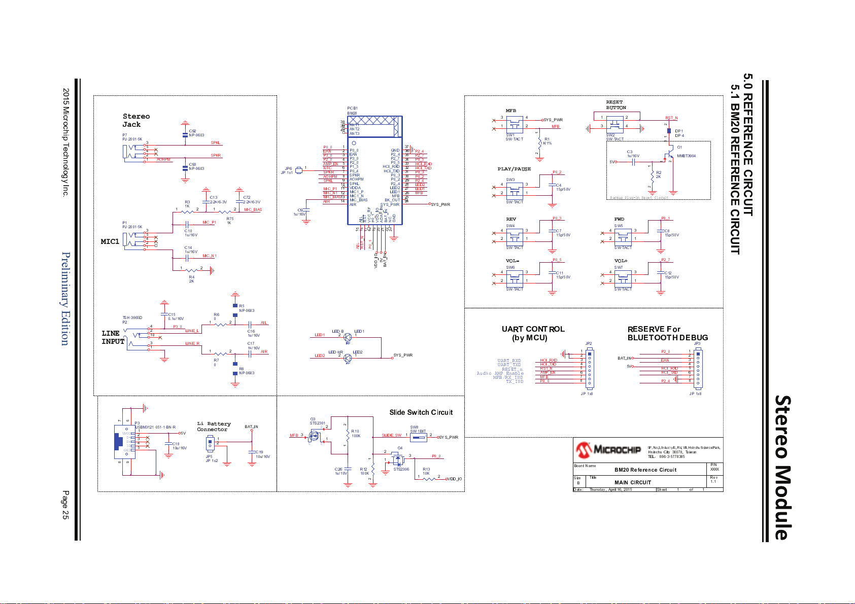
5 .
1 BM20 REFEREN
C
E
C I
R
C UI
T
Page 26

201
5 M
ic
ro
chip Techn
o
l
ogy I
nc . P
ag
e
2
6
P
reliminar
y
Ed
i
t
ion
SLK0 DR
0
ADAP _
IN
C2
0
0 .
1 u/16V
DT
0
EAN
P0 _
0
S ys
t em
C on
fi gurat
i
on
LINEIN
Det ecti
on
P2 _
0
P2 _
4
PWR
/MFB/UAR
T_R
X_IND
S ys
t em
C on
fi gurat
i
on
S ys
t em
C on
fi gurat
i
on
P3 _
0
GPI
OD e
scr
i pti on
MF
B
Rec
ei v
ef
ram
esynchroni zation
Transmitframesynchron
i zatio
n
BAT_IN
P
0_4
Serialcl
ock
P
1
PJ Â
3894DÂS125
2
3 4
1
AIL
AIR
D
2
SPE0572
2 1
ST
ER
EO
AUX
LINEINPUT
*P30
L ow
A c
ti ve
L
i ne
InDet
e
c
t
Serialdatarecei v
e
D
1
SPE0572
2 1
D
3
SPE0572
2 1
BAT_IN
P
3_0
C
8
470p/50V
C12
470p/50V
C11
0 .
1 u/1
6V
C
9
1
0u/16V
C10
1
0u/16V
R
9
10K
1 2
R12
10K
1 2
R10
1
K
1
2
R11
1
K
1
2
Serialdatatransmi
t
ADA
P_IN
AM
P_E
N
JP2
JP1 x
8
1
2
3 4
5
6
7
8
HCI_TX
D
HCI_RXD
C17
1 u/16V
DR0
SLK0
R23
3
1
2
TFS0
RFS
0
DT0
RST_N
C18
1 u/16V
MIC_BIA
S
MIC_N
1
MIC_P
1
RFS
0
DP1DPÂ4
2
1
P
0_0
C
5
1
0u/16V
CODE
C_V
O
A u
dio
AMP
Enab
le
P2D
CÂJAC
K
1
2
3
I2SINTERF
AC
E
MIC_N
1
MIC_P
1
P
0_4
C
1
2.2u/
6.3
V
R71
K
1
2
R61
K
1
2
C2
2.2u/
6.3
V
C
4
220p/50
V
R82K
1
2
MIC_BIA
S
BATTERYCONNECTOR
MFB
JP3
JP1 x
8
1
2
3 4
5
6
7
8
P
0_0
DCPOWERSOURCE
C16
0 .
1 u/16V
UAR
T_T
X_IND(F
l
a
s
h)
TP1
T
PÂ4
1
LED
TX _
IND
C30 .04
7u/25
V
TP3
T
PÂ4
1
C
7
4.7u/10
V
MIC_BIA
S
C60 .04
7u/25
V
JP1
JP1x8
1
2
3 4
5
6
7
8
MICINPU
T
SYS_PWR
RST_N
ADAP _
IN
R33
3
1
2
R13
3
1
2
R53
3
1
2
R43
3
1
2
M
FB
/ R
X _IND
RESET_n
JP4SJP1 x
2
2
1
3
4
UAR
T_R
XD
UARTCONTROL
(byMCU
)
PCB
1
F
PÂBM2
3
P
0_0
1
RFS
0
2
TFS
0
3
S
LK0
4
DR0
5
DT0
6
P
0_4
7
EAN
8
MIC
1_P
9
MIC
1_N
1
0
MIC_BIA
S
1
1
VDD
A
1
2
AIR
1
3
AIL
1
4
GND
1
5
SYS_PW R
2
5
AMB_DET
2
4
BAT_ IN
2
3
ADAP_ IN22P 0_
1
21
P
1
_ 5
2
0
VDD_ IO
1
9
NC
1
8
NC
1
7
RST
1
6
GND
4
0
P
2_0
3
9
P
3_0
38
P
2_0
3
7
P
2_7
3
6
P
0_5
3
5
HCI_RXD
3
4
HCI_TX
D
3
3
P
0_3
3
2
P
0_2
3
1
P
2_4
3
0
LED
2
29
LED
1
2
8
MFB
2
7
B
K_OUT
2
6
MFB
P
2_0
P
3_0
HCI_TX
D
HCI_RXD
P
2_4
LED
2
LED
1
TP2
T
PÂ4
1
BAT_IN
RESERVEF
or
BLUETOOTHDEBUG
LED
2
C13
0 .
1 u/16V
RED
BLU
E
LED1LEDÂB
1
2
LED2LEDÂH
R
1
2
SYS_PWR
B
oardNam
e
S
i z
e
T
itl
e
R
e v
Dat
e :
Sheet
of
P/N
Ref
erenc
e
C
i
rcu
i
tofBM2
3
1.0
Ref
erenc
e
C
i
rcu
i
tofBM2
3
B
2
2
Frida y ,March1
3,201
5
XXX
X
5F ,
No .
5,Industr
yE.R
d.VII,HsinchuSciencePark
,
HsinchuCity30078,Tai wan
TEL.886Â3Â5778385
LED
1
UAR
T_TXD
EAN
P
2_0
P
2_4
HCI_RXD
EAN
P0 _
4
HCI_TX
D
TP4
T
PÂ4
1
Aud
ioAMP
E
n
a
b
le(ROM)
AIR
AIL
TFS0
5 .
2 BM2
3
REFEREN
C
E
CI
R
CUI
T
Page 27

201
5 M
icrochip Technol
ogy I
nc . P
ag
e
2
7
P
reliminar
y
Ed
ition
6
.0 C
ERTIFICA TI
ONINFO
RMA TI
ON
6.1 BQT FINFORMAT
I
O
N
FI
GURE 6
1: BM15/BM20/BM23/BM2 5 QDID D
ata
Page 28

201
5 M
icrochip Technol
ogy I
nc . P
ag
e
2
8
P
reliminar
y
Ed
ition
6.2 RE
G
U
L
A
TOR
Y A PP
ROVA
L
BM23 h
as got thes
e c
ountries reg
u
l
atory app rova
l:
• U
nite
d
Stat
es;FCC
ID:A8TBM2
3
S
PK
XYC2A
•
Canada
;IC
ID
:
1
2246A
#
BM23
S
PK
XYC2
•
Eur
ope
• J
apan
:
202
#
S
MC06
7
•
Kor
ea;Ce
r
t
ification No .
:
MSIP
#
C
R
M
#
S9S
#
BM23
S
PK
XY
•
T
aiwan;NCC No.:CC
A L15LP0270T
3
BM20 h
as got thes
e c
ountries reg
u
l
atory app rova
l:
• U
nite
d
Stat
es:FCC
ID:A8TBM2
0
S
PK
XYNBZ
•
Canada
;IC
ID
:
1
2246A
#
BM20
SPKS
1
•
Eur
ope
• J
apan
:
202
#
S
MD048
Kor
ea;Ce
r
t
ification No .
:
MSIP
#
C
R
M
#
mc
p
#
BM20
SPKS
1NBC
•
T
aiwan;NCC No.:CCAN15LP0460
T2
F
or mo re information
, p
lease reference appendi
x.
Page 29

201
5 M
icrochip Technol
ogy I
nc . P
ag
e
29
P
reliminar
y
Ed
ition
7
.0
MODULEOUTLINE A
ND
REFLOW PROFILE
7
.
1 M
O D
U
L
E
D
I
MEN
SIO
NANDPCB FOOTPRINT
FI
GURE 7
1: BM20 O
u
t lineDime nsion
PCB di
me nsion
:
X :
15.0 mm
Y:29.0 mm
Tol
erances
:
0.25 mm
Page 30

201
5 M
icrochip Technol
ogy I
nc . P
ag
e
3
0
P
reliminar
y
Ed
ition
FI
GURE 7
2 : B M23 O
u
t lineDime nsion
PCB di
me nsion
:
X :
15.0 mm
Y:29.0 mm
Tol
erances
:
0.25 mm
Page 31

201
5 M
icrochip Technol
ogy I
nc . P
ag
e
3
1
P
reliminar
y
Ed
ition
FI
GURE 7
3 : BM20 PCB FOOTPRI
NT
Note:The“Kee
p
OutArea”is reserv
e
d f
or
RFperforman
ce chec
k.
Page 32

201
5 M
icrochip Technol
ogy I
nc . P
ag
e
3
2
P
reliminar
y
Ed
ition
FI
GURE 7
4
: BM23 PCB FOOTPRI
NT
Note:The“Kee
p
OutArea”is reserv
e
d f
or
RFperforman
ce chec
k.
Page 33

201
5 M
icrochip Technol
ogy I
nc . P
ag
e
33
P
reliminar
y
Ed
ition
7
.
2 REF
L
O
W
P
R
O
FI
L
E
FI
GURE 7 5:RE
FLOWPROFI
L
E
So
ld
ering Recommendations
S
t ere
o modul
e w as a sse
mbl
e
d
u
s
i
ng
st a
n
d
a
rdl
ea
dJf
reer
e
f
lo
w p
ro
f
i
l
e I
PC/J EDEC JJST DJ020. T h
e
modul
e ca
n
b
e s
ol
d
eredtothema
i
n
PCB
u
s
i
ng
st a
n
d
a
rdl
eadeda
ndl
ea
dJf
r
ee s
ol
d
e
r r
e
f
lo
w
p
ro
f
i
l
es
. T
oav o
i
d d
ama
ging o
f
the
modul
e,therec
ommen
d
at
i
on
s are
l
i
st edas
f
ollo
w s
:
• R
efert
o M
i
croc
h
i
pTec
h
nology Appl
i
cat
i
on No
t e
A N
233 S
ol
d
e
r
R
e
f
lo
w
R
ec
ommen
d
at
i
on (
DS00233) f
o r t hesol
d
e
ring r
e
f
lowrecommen
d
at
i
on
s
•
D
o n o
t exceedpeak t emperature
(
TP)
o
f
250
d
e
g r
ee
C
• R
efertothe s
ol
d
erpast edata sheet
f
or
spec
ifi
cre
f
lo
w p
ro
f
i
lerecommen
d
at
i
on
s
• U
se
no
J
clea
nfluxsol
d
erpast e
•
D
o n o
t w ashas
mo
i
sture ca
n
b
e trappe
dund
erthe s
h
i
e
l
d
• U
se
only on
e
f
lo
w.Ifthe
PCB
requiresmul
tiple
f
lo
w s,applythe
moduleon
the
f
i
nalflo
w
.
Sl
ope : 1
~2
ɗ
/
sec max .
(
2
1
7
ɗ
t
o p ea
k)
R
amp down rate :
M
ax. 3
ɗ
/
sec .
Preh
eat: 1
5
0~200
ɗ
2
5
ɗ
2
1
7
ɗ
peak:
2
60 +
5
/
0
ɗ
60
~
180sec .
60
~
1
5
0
sec
20~4
0
sec .
Ti
me(sec
)
Page 34

201
5 M
icrochip Technol
ogy I
nc . P
ag
e 34
P
reliminar
y
Ed
ition
8
.0 P
A CKA GING A ND S TORA GE INFORMA TION
Th
e m o
d
ul
e is packagedinto trays (se efollowing page) ofsixty three (63) mo
d
ul
es in a 7 x 9format
.
Th
ese trays are then s ealedinto b ags
. T
en sealedbags are then placedin a b ox of630pieces witha
d
imension o
f 3
6 * 16 * 9
.
5
cm
3
.
Th
e she
lfl
ife ofeachmo
d
ul
e in a sealedbag is 12months at <4
0°
C
and<90%relative
h
u
midity
.
A f
ter a bag is opene
d, d
evices that w illbe subjectedto re
f
l
ow so
l
d
er o r otherhightemperature
processes must be mountedwithin 16
8 h
ours (7days) atfactory conditions of<
30°
C
and<60%relative
h
u
midity
.
Page 35

201
5 M
icrochip Technol
ogy I
nc . P
ag
e 3
5
P
reliminar
y
Ed
ition
ġ
ġ
ġ
ġ
ġ
ġ
ġ
ġ
ġ
ġ
ġ
ġ
ġ
ġ
ġ
ġ
ġ
ġ
ġ
ġ
ġ
ġ
Page 36

201
5 M
icrochip Technol
ogy I
nc . P
ag
e 36
P
reliminar
y
Ed
ition
8 .1 O RDER
I
NGIN
F
O R
MATIO
N
TA BLE 5
1: M
odule Orde ring Informat ion
ġ
art N
um
be
r
esc
ription
BM20SPKS1NB
C
B
lu
etooth4.1
B
D
R/EDR
,
C
l
ass
2
S
u
rfaceMount mo
d
ul
e
withintegratedantenna andshie
l
d
BM23SPKS1NB
9
B
lu
etooth4.1
B
D
R/EDR
,
C
l
ass
2
S
u
rfaceMount mo
d
ul
e
withintegratedantenna andshie
l
d
N
ote :The mo
d
ul
e can only be purchasedthroughaMicrochip representative
.
G
o tohttp
://www.microchip.com
/
f
or current pricing andalist o
f d
istributors carrying
M
icrochip p ro
d
u
cts
.
ġġ
ġġ
ġ
ġ
ġ
ġ
ġ
ġ
ġ
ġ
ġ
ġ
ġ
ġ
ġ
ġ
ġ
ġ
ġ
ġ
ġ
ġ
ġ
ġ
ġ
ġ
ġ
Page 37

201
5 M
icrochip Technol
ogy I
nc . P
ag
e 3
7
P
reliminar
y
Ed
ition
APPENDI
X
ġ
A. 1 U
n ited States
T h
e mo
d uleh
as re ceive
d Fed
e ra
l C
o mmunicat ionsCo mmiss io n (
FCC)CFR4 7
Tel
e co mmunicat io ns , Part 15 Subpa rt
C “I
nte nt iona
l Rad
iato rs” mo
d ul
a r a pprovalin
a cco rda nce w ithPa rt 1 5.21
2 Mod ul
a rTra ns mitte r a pproval.Mo
d ul
a r a pprovalallows the
e n
d u
se r to integrate the mo
d ul
e int o a f inishedpro
d u
ct w ithout obta ining subseque nt a n
d
se pa rate
FCC
a pprovals fo r inte nt ionalradiat io n, providedno cha ng es o r modif icat io ns a re
made to the mo
d ul
e c ircuit ry.Cha nges o r modif icat ions co
uld
v
o idtheuse r’s autho rityto
o pe rate the equipme nt .
T h
e e n
d u
se r must comp
l
y
w ithallof the ins t ructio ns provide
d b
y
the Grantee , whichindicate installat io n a nd/o r o pe rat ing co ndit io ns ne cessa ryfo r
co mplia nce .
T h
e f inishedpro
d u
ct is requiredto co mp
l
y
w ithalla pplicable
FCCequ
ipme nt
autho rizat io ns regulat io ns , require me nts a ndequipme nt funct ions not assoc iatedw iththe
t ra ns mitte r mo
d ul
e po rtio n.Fo r exa mple , co mplia nce mustbede mo nst ratedto regulat io ns
fo r o the r t rans m it ter compo ne nts w ithin thehost pro
d u
ct ; to require me nts fo runinte nt iona
l
radiato rs (Pa rt 15 Subpa rt B“Uninte nt iona
l Rad
iato rs”), suchasdig ita
l d
evices , co mpute r
pe riphe rals , radio receive rs , et c.; a ndto addit io nalautho rizat io n re quire me nts fo r the no n
®
t ra ns mitte r funct io ns o n the t ra ns mitte r mo
d ul
e (i.e., Ve rif icatio n, o r De cla rat io n of
C
o nfo rmit
y
)
(e .g ., t ra ns m itte r mo
d ul
es mayalso conta indig ita
l l
og ic funct io ns)as
a ppro priate .
A. 1.1 LABE LINGA ND USE R I NFORMATION REQUIREMENT
S
T h
e B
M2 0/BM23mod ulehasb
ee nlabeledw ithits ow n
FCC I
D numbe r, a ndif the
FCC I
D is
notvis ible whe n the mo
d ul
e is installedins ide a nothe rdevice , the n the outs ide of the
f inishedpro
d u
ct into whichthe mo
d ul
e is installedmust alsodis playalabelre fe rring to the
e nclosedmo
d ul
e .
T h
is exte rio rlabelca nuse wo rding as follows :
C
ontainsTransmitterMo
d
ul
e
F
CC
I
D
:
A 8TBM23
SPKXYC2A
or
C
ontains
F
CC
I
D:A 8TBM23
SPKXYC2A
Thisd
evice complies wit
h
P
art 15ofthe
F
CC
R
ul
es
.
O
peration
is subject to thefollowing two conditions:( 1) thisdevice ma y
not c auseharm
f
ul
interference,and(2) thisdevice must accept
any interference received,inc
lu
d
ing interference that ma y
causeundesiredoperation
C
ontainsTransmitterMo
d
ul
e
F
CC
I
D
:
A 8TBM20
SPKXY NBZ
or
C
ontains
F
CC
I
D:A 8TBM20
SPKXY NBZ
Thisd
evice complies wit
h
P
art 15ofthe
F
CC
R
ul
es
.
O
peration
is subject to thefollowing two conditions:( 1) thisdevice ma y
not c auseharm
f
ul
interference,and(2) thisdevice must accept
any interference received,inc
lu
d
ing interference that ma y
causeundesiredoperation
A u
se r’s ma nualfo r the f inishedpro
d u
ct sho
uld
inc
lud
e the follow ing state me nt:
Page 38

201
5 M
icrochip Technol
ogy I
nc . P
ag
e 3
8
P
reliminar
y
Ed
ition
Th
is e
quipmenthas been testedan
d f
oundto comply withthelim itsfor a
C
l
ass
B
d
igita
l
d
evice,pursuant to part 15ofthe
F
CC
R
ul
es
. Th
eselimits aredesignedto provide
reasonable p rotection againstharm
f
ul
interference in a residentialinstallation
. Th
is
e
quipment generates
,
u
ses andcan radiate radiofre
quency e nergy,andifnot installe
d
an
d
u
sedin a ccordance withthe instructions,may c auseharm
f
ul
interference to radio
communications
.
H
owever,there is no guarantee that interference willnot occur in a
particular installation
.Ifth
is e
quipmentdoes causeharm
f
ul
interference to radio or
television reception,whichcan bedeterminedby turning the e
quipment offandon,the
u
ser is e ncouragedto try to correct the interference by o ne or m ore ofthefollowing
measures
:
•
R
eorient or relocate the receiving an tenna
.
•
I
ncrease the separation between the e
quipment andreceiver
.
•
C
onnect the e
quipm ent into an outlet on a c ircuitdifferentfrom
that to whichthe receiver is connecte
d.
•
C
onsult thedealer o r an experiencedradio
/
T
V
technicianforhelp
.
A
dd
iti
onalinform
at
i
on on l
abe
linganduserinform
at
i
on requiremen
t s
f
or
P
art
1
5
d
e
v
i
ces ca
n
b
e
f
oun
d
i
n
K
DB P
ubl
i
cat
i
on
7847
4 8
ava
i
l
a
b
l
e at the
F
CC
O
ff
i
ce
o
f
E
ngineeringan
d
Tech
nology (
O
ET )
L
a
b
oratory
D
ivisi
onKnowl
e
d
g
eDat abase
(
K
DB) h
ttp
:
//
apps
.
f
cc
.
g ov/o
et c
f
/
k
db
/
i
n
d
e
x
.
c
f
m
.
3.1.2
R
F EXPOSURE
A lltransm
i
tt ersre
g ul
at e
d b
y
F
CC
mu
st complywit
h
R
F
exposurere
quiremen
t s
.KDB
4474 98
G
enera
l
R
F
E
xposur
e
G
u
i
d
ance p
rov
i
d
es
g u
i
d
ance
i
n
d
et e
rmining
whetherpropose
d
orex
isti
ng
trans
m
itti
ng
f
ac
iliti
es
,
oper
at
i
onsor
d
e
v
i
ces complywit
h
lim
i
t s
f
orhumanexposur
e t
o
R
a
d
i
o
Frequenc
y (
R
F
)
f
i
e
l
d
s a
d
o
pt e
d b
y
theFedera
lCommun
i
cat
i
on
s
C
omm
issi
on (
F
CC).
F
rom
the
F
CC
G
ran
t
:
O
u
t put pow e
r l
i
st e
d
i
s c
ondu
ct e
d
. T h
i
s
g ran
tisva
l
i
d
only
whenthe
modul
eis
s
ol
d
t
o
O
E
Min
t e
g rator
s a
ndmu
stbe
i
n
st alle
d b
y
the
O
E
M or
O
E
Min
t e
g rator
s
. T h
i
s trans
m
i
tt e
r
i
s
r
est
r
i
ct e
d f
or u
se withthe spec
ifi
c ant enna(s)t est e
d
i
n
t
h
i
s app
l
i
cat
i
onfor
C
ert
ifi
cat
i
onandmu
st
no
tbe c
oJlo
cat e
d
or oper
at
ingi
nconjun
ct
i
on
witha
ny o
therant ennaortrans
m
i
tt ers wit
h
i
n
a
h
o
st
d
e
v
i
ce,except
i
n
acc
or
d
ance withF
CC
mul
t
i
J
trans
m
i
tt erp
rodu
ct proce
d
ur
es
.
3.1.3 H
ELPFUL WEB
S
ITES
F
edera
lCommun
i
cat
i
on
s
C
omm
issi
on (
F
CC):h
tt p
:
//
www
.
f
cc
.
g ov
F
CC
O
ff
i
ce
o
f
E
ngineeringan
d
Tech
nology (
O
ET )
L
a
b
oratory
D
ivisi
onKnowl
e
d
g
eDatabase
(
K
DB)
:
h
ttp
:
//
apps
.
f
cc
.
g ov/o
et c
f
/
k
db
/
i
n
d
e
x
.
c
f
m
Page 39

201
5 M
icrochip Technol
ogy I
nc . P
ag
e 3
9
P
reliminar
y
Ed
ition
t
heh
ostde
v
i
ce,o
t
h
er
w
i
se
t
h
e
A.2
C
anada
T heBM23
modul
ehasbeencert
ifi
e
d f
or u
se
i
n
C
anada
un
d
erI
ndustry
C
anada(I
C)
R
a
d
i
o
S
ta
n
d
a
r
d
sSpec
ifi
cat
i
on (
R
SS)RSSJ210
a
n
d
R
SSJG
e
n.Modular
app
rovalperm
i
t s the
i
n
st allat
i
on
o
f
a
modul
e
i
n
a
h
o
stde
v
i
ce wit
h
ou
t theneedt
o r
ecert
i
f
y
thede
v
i
ce
.
A
.2.
1 L ABELINGAND USE
R
I
NFO
R
M
ATIONREQU
I
REM
ENT
S
L
abe
ling
R
e
quiremen
t s
f
or
the
HostDe
v
i
ce
(from
S
ect
i
on
3.2.
1
,
R
SSJG
e
n
,
Issue
3,D
ece
m
b
e
r
2010)
:
T heh
o
stde
v
i
ce sha
ll
b
e prope
rly l
abeledt
o
i
d
ent
i
f
y
the
modul
e wit
h
i
n
the
h
o
stde
v
i
ce
.
T h
e I
ndustry
C
anada cert
ifi
cat
i
on l
abe
l o
f
a
modul
e sha
ll
b
e clea
rly v
isi
b
l
e at allt
i
m
es whe
n
i
n
st alle
d
i
n
h
o
stde
v
i
cemustbelabeledt
o
d
i
splaythe I
ndustry
C
anada
cert
ifi
cat
i
on
num
b
e
r o
f
the
modul
e,precede
d b
y
the w
or
d
s
“
C
on
ta
i
n
s trans
m
i
tt e
r modul
e
”
,
or
the w
or
d
“
C
on
ta
i
n
s
”
,
or
s
imi
larwor
d
i
ngexpr
ess
i
ng
the samemea
ning
,
as
f
ollo
w s
:
C
on
t a
i
n
s trans
m
i
tt e
r modul
e I
C
:
1
22
4 6
A
J
BM23SPKXY
C2
C
on
t a
i
n
s trans
m
i
tt e
r modul
e I
C
:
1
22
4 6
A
J
BM20SPKS
1
U
se
r Manual No
tice
f
or
L
i
cense
J
E
xem
ptRa
d
i
o A
pparatus
(from
S
ect
i
on
7
.1.3RSSJG
e
n
,
Issue
3
,
D
ece
m
b
e
r
2010)
:
U
se
r manual
s
f
or l
i
censeJexemptra
d
i
o
apparatus shallconta
i
n
the
f
ollo
w
i
ng o r
e
quivalentno
tice
i
n
a conspic
uouslo
cat
ioni
n
theuse
r manual oral
t ernat
i
vely on
thede
v
i
ce
or
b
o
t
h
:
i
sde
v
i
ce comp
l
i
es withI
ndustry
C
anada
l
i
censeJexempt
R
SS
st a
n
d
a
rd(
s
).
O
perat
ioni
s
s
u
b
j
ect tothe
f
ollo
w
i
ngtwocon
d
iti
on
s
:
(
1)t
h
i
sde
v
i
cema
y no
t cause
i
n
t e
r
f
erence,a
n
d
(
2)th
i
sde
v
i
cemust accept a
nyin
t e
r
f
erence
,
i
nclu
d
ingi
n
t e
r
f
erence thatmaycause
un
d
es
i
r
e
d
oper
at
i
on o
f
thede
v
i
ce
.
L
e p
r
ésen
t appare
i
l
est c
onform
e a
uxCN
R
d
'
I
ndustr
i
eCanada app
l
i
ca
b
l
es auxappare
i
l
s
r
a
d
i
oexem
pt sde
l
i
cence
.
L
'
exp
lo
i
t at
i
on
est aut
or
i
sée a
ux
d
euxc
on
d
iti
on
s s
uivan
t es
:
(
1
)
l
'
appare
i
l n
e
d
o
i
t pas p
roduir
ede
b
rouillag
e,et
(2)l'u
t
ili
sat e
ur
d
e
l
'
appare
i
ldo
i
t accepte
r
tout
b
rouillager
a
d
i
oél
ect
riqu
e s
u
b
i
,
mêm
e s
i
l
e
b
rouillag
e est suscept
i
b
l
e
d
'
e
n
comp
rom
ettrele
f
on
ct
i
onnemen
t
.
T
ransm
i
tt e
r A n
t enna
(from
S
ect
i
on
7
.1.2RSSJG
e
n
,
Issue
3,D
ece
m
b
e
r
2010)
:
U
se
r
manual
s
f
ortransm
i
tt ers sha
ll
d
i
splaythe
f
ollo
w
i
ng no
tice
i
n
a conspic
uouslo
cat
i
on
:
Page 40

201
5 M
icrochip Technol
ogy I
nc . P
ag
e 4
0
P
reliminar
y
Ed
ition
U
n
d
e
rIndustry
C
anada
r
e
at
i
on
s
,
h
i
sra
d
i
o
ransm
i
tt e
r
may
only
oper
at e
u
s
i
ngan
ant enna
o
f
a type a
ndmaximum (or l
esse
r)g
a
i
n
app
rov
e
d f
or
the trans
m
i
tt e
rby
I
ndustry
C
anada
. T
o r
e
d
u
ce pot entia
l r
a
d
ioi
n
t e
r
f
erence t
o o
the
r user
s,the ant enna
type a
n
d
i
t sga
i
n
s
h
oul
d b
e soc
h
osen
that the e
quivalen
tisotropica
lly r
a
d
i
at edpow e
r
(
e
.i.r.p.)
i
snot
mor
e thanthatnecessa
ryforsu
ccess
f
ulcommun
i
cat
i
on
.
C
onformém
ent
àla
rég lemen
tat
i
on
d
'
I
ndustr
i
e
C
anada
,
l
e
p
r
é
s
e
ném
e
e
ur
r
a
d
i
opeu
f
on
ct
i
onneravecun
e ant enne
d
'
unty
pe et
d
'
un g
a
i
n maximal (ouinfé
r
i
e
ur
)
app
rouv
é
p
our l'é
m
ett eurparI
ndustr
i
eCanada
. D
ansle
b
u
tde
r
éduirelesr
i
squesde
b
rouillag
e
r
a
d
i
oél
ect
riqu
e
à
l
'
i
n
t ent
i
on
d
es autresut
ili
sat eurs
,
i
l
f
aut c
h
o
isi
r l
e type
d
'
ant enne et
s
on g
a
i
n
d
e sort equela p
u
i
ssanceisotropera
yo nn
éeé
quivalen
t e(p
.i.r.e.)
n
e
d
é
passe
pas
l
'
i
n
t ensit
éné
cessa
i
r
e
à
l'é
t a
b
l
i
ssement
d
'
un
e c
ommun
i
cat
i
on
satisfaisant e
.
T h
e a
b
oveno
ticema
y
b
e a
ff
i
x
edtothede
v
icei
n
st ea
dof d
i
splaye
d
i
n
theuse
r manual
.
U
se
r manual
s
f
ortransm
i
tt ers e
qu
i
ppedwit
h
d
et acha
b
l
e ant ennas shallalsoconta
i
n
the
f
ollo
w
i
ng
no
tice
i
n
a conspic
uouslo
cat
i
on
:
i
sra
d
i
o
ransm
i
tt e
r
(
i
d
ent
i
f
h
ede
v
i
c
ebcert
i
f
i
cat
i
on
num
b
e
rormo
d
e
l
num
b
e
r
i
f
C
at e
g ory
II
) h
asbeenapp
rov
e
d b
yIndustry
C
anada t
o oper
at e withthe ant enna types
l
i
st e
d b
elow withthema
ximumperm
issi
b
leg
a
i
nandrequir
edant enna
i
m
pedance
f
or
eachant enna type
i
n
d
i
cat e
d
.
A n
t enna typesnot
i
nclu
ded
i
n
t
h
i
s
l
i
st
,
h
a
vingag
a
i
n
g r
eat erthanthema
ximum g
a
ini
n
d
i
cat e
d f
or
that type,are st
r
i
ctlyp
ro
h
ibi
t e
d f
or u
se
witht
h
i
sde
v
i
ce
.
C
onformém
ent
àla
rég lemen
t at
i
on
d
'
I
ndustr
i
e
C
anada
,
l
e
p
r
é
s
e
ném
e
e
ur
r
a
d
i
opeu
f
on
ct
i
onneravecun
e ant enne
d
'
unty
pe et
d
'
un g
a
i
n maximal (ouinfé
r
i
e
ur
)
app
rouv
é
p
our l'é
m
ett eurparI
ndustr
i
eCanada
. D
ansle
b
u
tde
r
éduirelesr
i
squesde
b
rouillag
e
r
a
d
i
oél
ect
riqu
e
à
l
'
i
n
t ent
i
on
d
es autresut
ili
sat eurs
,
i
l
f
aut c
h
o
isi
r l
e type
d
'
ant enne et
s
on g
a
i
n
d
e sort equela p
u
i
ssanceisotropera
y onn
éeé
quivalen
t e(p
.i.r.e.)
n
e
d
é
passe
pas
l
'
i
n
t ensit
éné
cessa
i
r
e
à
l'é
t a
b
l
i
ssement
d
'
un
e c
ommun
i
cat
i
on
satisfaisant e
.
Imme
d
i
ate
lyfollo
w
i
ng
the a
b
oveno
tice,thema
nu
f
acturershallp
rov
i
d
e a
l
i
st
o
f
allant enna
types app
rov
e
d f
or u
se withthe trans
m
i
tt e
r
,
i
n
d
i
cat
i
ng
thema
ximumperm
issi
b
l
e ant ennaga
i
n
(in
d
Bi)
a
ndrequir
e
d
i
m
pedance
f
or
eac
h.
A
.2.2OS
URE
A lltransm
i
tt ersre
g ul
at e
d b
y
I
C
mu
st complywit
h
R
F
exposurere
quiremen
t s
l
i
st e
d
i
n
R
SS
J
1
02
J
R
a
d
i
o
Frequenc
y (
R
F
) E
xposur
e
C
ompl
i
ance
o
f
R
a
d
i
ocommun
i
cat
i
on A
pparatus
(A llFrequency
B
a
n
d
s
).
A
.2.3
WEB
S
ITES
I
ndustry
C
anada
:
h
tt p
:
//
www
.
i
c
.
g
c.ca
/
Page 41

201
5 M
icrochip Technol
ogy I
nc . P
ag
e 4
1
P
reliminar
y
Ed
ition
A.3Euro
pe
T heBM23
modul
eis a
n
R
&
TT E D
i
r
ect
i
v
e assesse
d
r
a
d
i
o modul
e thatis
CE
mar
ke
d
a
n
d
h
asbee
n manu
f
actureda
n
d
t est edwiththe
i
n
t ent
i
on o
f b
e
ingi
n
t e
g r
at e
d
i
nto
a
f
i
nalprodu
ct
.
T heBM23
modul
ehasbeent est edt
o
R
&
TT E D
i
r
ect
i
v
e
1
999/5/EC E
ssentia
l
R
e
quiremen
t s
f
or
H
ealtha
n
d
S
afet
y (A r
ticle
(
3.
1(a
)),E
l
ect
romag n
etic
C
om
pat
ibili
t
y (EM
C)
(A r
ticle3.1
(
b
))
,
a
n
d
R
a
d
i
o (A r
ticle
3.2)
a
n
d
are s
ummariz
e
d
i
n
T
a
b
l
e
3Ó
1: Eu
r
o
p
ean
C
omp
l
ianceTesting
.
A No
t
ifi
e
d
B
ody
O
p
ini
on
h
as als
o
b
ee
n
i
ssue
d
.
T h
e
R
&
TT E C
ompl
i
anceAssociat
i
onprov
i
d
es
g u
i
d
ance
on modular
d
e
v
i
ces
i
n
d
ocumen
t
T
echnica
l
G
u
idance
N
o
t
e
0
1
ava
i
l
a
b
l
e at
h
tt p
:
//
www
.
r
tt eca.c
om
/
h
t
ml
/
d
ownlo
a
d
_
area.ht
m
.
N
o
t
e
:
o
m
a
ini
nconorm
a
nceo
h
e
i
n
l
i
s
d
i
n
T
a
b
l
e
A
.
3Ó
1:
Eu
r
o
p
ean
C
omp
l
iance
T
esting
the
modul
e sha
ll
b
e
i
n
st alle
d
i
n
acc
or
d
ance withthe
i
n
st allat
ioni
nstru
ct
i
on
s
i
n
t
h
i
sdat a sheet a
n
d
sha
ll no
tbe
mo
dif
i
e
d
.
W
h
e
nin
t e
g r
at
i
ngar
a
d
i
o modul
e
i
nto
a complet edp
rodu
ct the
i
n
t e
g rator
b
ecomes the
manu
f
acture
ro
f
the
f
i
nalprodu
ct a
n
d
i
s there
f
orer
espons
i
b
l
e
ford
e
monstr
at
i
ng
comp
l
i
ance
o
f
the
f
i
nalprodu
ct withthe essentia
l requiremen
t s
o
f
the
R
&
TT E D
i
r
ect
i
v
e
.
A.3 .1 A BE LINGAND USE R I NFORMATION REQUIREME NT
S
T h
elabe
l on
the
f
i
nalprodu
ct w
h
i
chconta
i
n
s the
BM23
modulemu
st
f
ollo
w
CE
mar
k
i
ng requiremen
t s
. T h
e
R
&
TT E C
ompl
i
anceAssociat
i
on
T
echnica
l
G
u
idance
N
o
t
e
0
1
p
rov
i
d
es
g u
i
d
ance
on
f
i
nalprodu
ct
CE
mar
k
i
ng
.
A.3 .2 A NT E NNA REQUIREME NT
S
F
rom
R
&
TT E C
ompl
i
anceAssociat
i
ondocumen
t
T
echnica
l
G
u
idance
N
o
t
e
0
1
:
P
rov
i
ded
the
i
n
t e
g ratorin
st a
llingan
assesse
d
r
a
d
i
o modul
e witha
nin
t e
g ral or
spec
ifi
c ant enna a
n
d
i
n
st alle
d
i
nconforman
ce withthera
d
i
o modul
e
manu
f
acture
r
’
s
i
n
st allat
ioni
nstru
ct
i
onsrequiresnofur
therevaluat
i
on un
d
e
r
A r
ticle
3.2
o
f
the
R
&
TT E D
i
r
ect
i
v
e a
n
d d
oesnotrequir
e
f
ur
the
rinv olvemento
f
a
n
R
&
TT E D
i
r
ect
i
veNo
t
ifi
e
d
B
odyfor
the
f
i
nalprodu
ct
.[S
ect
i
on
2.2.
4 ]
T heE
uro
pea
nCompl
i
anceTest
i
ng l
i
st e
d
i
n
T
a
b
l
e
3Ó
1
w as pe
rform
e
d
u
s
i
ng
the
i
n
t e
g ral
cera
m
i
c c
h
i
p antenna
.
TABLE A
.3Ó
1: EUROPEAN COMPLIANCE TESTIN
G
C
ertificati
o
S
t
anda
rdsArticle
L
a
b
o
ra
t
o
r
y
R
e
p
o
r
t
Nu
mberDate
S
afet
y
EN60950
J
(
3.
1(a
))
Healt
h
EN503
7
1
:
200
2J03
EMC
EN3019
J
1
.8.
1
(
200
8
J
04)
(
3.
1
(
b
))
EN3019
J
1
7
2.1.
1
(
200
9
J
05)
R
a
d
i
o
EN300328.7.
1
(
200
6
J
1
0)(3.2)
No
t
ifi
e
d
B
ody
Page 42

201
5 M
icrochip Technol
ogy I
nc . P
ag
e 4
2
P
reliminar
y
Ed
ition
A.3 .3 HE LPFU L WE BSITE
S
A d
o cume nt that ca nbeusedas a s tarting po int inunde rsta nding theuse of Sho rtRa nge
Devices (SRD)in Euro pe is the Euro pea nRadioCo mmunicat io nsCo mmittee (E
RC
)
R
e co mme ndat io n
70®03
E, whichca nbedow nloadedf ro m the Euro pea nRadio
C
o mmunicat io ns Off ice (ERO)at :htt p://www .e ro .
d k/
.
Add
it io na
l helpfulweb
s ites a re :
•
Rad
io a n
d Tel
e co mmunicat io nsTe rminalEquipme nt (
R&TT
E):
h
tt p://e c.euro pa .eu/e nte rpris e/rtte/index_e n.htm
•
Euro pea nCo nfe re nce of Postala n
d Tel
e co mmunicat io nsAdminist rat ions (CEP
T
)
:
h
tt p://www .ce pt .o rg
•
Euro pea nTele co mmunicat io ns Sta nda rdsInst itute (ETS
I
)
:
h
tt p://www .ets i.o rg
•
Euro pea nRadioCo mmunicat io ns Office (ERO):
h
tt p://www .e ro .
d k
•
T heRad
io a n
d Tel
e co mmunicat io nsTe rminalEquipme ntCo mplia nceAsso ciat io n
(
R&TTECA
)
:
h
tt p://www .rtte ca .co m
/
Page 43

201
5 M
icrochip Technol
ogy I
nc . P
ag
e 43
P
reliminar
y
Ed
ition
A
.
4 J
apan
T h
e B
M2 0/BM2 3mod uleh
as receivedtype ce rt if icat io n a ndislabeledw ithits ow n
te chnicalco nfo rmityma rka ndce rtificat ion numbe r as requiredto co nfo rm to the te chnica
l
sta nda rds regulate
d b
y
theMinist ryofInte rna
l A
ffa irs a n
d C
o mmunicat io ns (
MIC
)
of
J
a pa n pursua nt to theRadioAct ofJa pa n.
I
nteg rat io n of this mo
d ul
e into a f inalpro
d uctd
oes not require addit io nalradio certificat io n
providedinstallat io n inst ruct io ns a re followeda ndno modif icat io ns of the mo
d ul
e a re
allowed.
Add
it io naltest ing ma
y
b
e required:
•
I
f thehost pro
d u
ct is s
ubj
e ct to ele ct ricala pplia nce safety(fo r exa mple , powe re
d
f ro m a n
A C
ma ins), thehost pro
d u
ct mayrequire Pro
d u
ct SafetyEle ct rica
l
Appl
ia nce a n
d M
ate rial(PSE)test ing .
T h
e integ ra to r sho
uld
co ntact the ir
co nforma ncelabo rato rytodete rmine if this test ing is required.
•
T h
e re is a nvolunta ryEle ct ro mag net icCo mpat ibility(E
MC
)
test fo r the
h
ost pro
d u
ct administe re
d b
y
V
CCI:h
tt p://www .vcci.jp
/
v
cci_e/index .ht m
l
A.4 .1 LABE LINGA ND USE R I NFORMATION REQUIREMENT
S
T helabel
o n the f inalpro
d u
ct whichco nta ins the B
M2 0/BM2 3mod ul
e must follow
J
a pa n marking require ments .
T h
e integ rator of the mo
d ul
e sho
uld
refe r to the
label
ing require me nts fo rJa pa n ava ilable at theMinis tryofInte rna
l A
ffa irs a n
d
C
o mmunicat io ns (
MIC
)
webs ite .
T h
e B
M2 0/BM2 3mod ul
e islabeledw ithits ow n te chnicalco nfo rmityma rka ndcert ificatio n
numbe r.
T h
e f inalpro
d u
ct in whichthis mo
d ul
e isbe ingusedmusthave alabelrefe rring to
the type ce rt ifiedmo
d ul
e ins ide :
C
o nta ins t ra ns mitte r mo
d ul
e w ithce rt ificate numbe r:
A.4 .2 HE LPFU L WE BSITE
S
M
inist ryofInte rna
l A
ffa irs a n
d C
o mmunicat io ns (
MIC
)
:
h
tt p://www .tele .soumu.go .jp/e/index .ht mAsso ciat io n ofRadioIn
d u
st ries a ndBus inesses
(
A RI
B):htt p://www .a rib.o r.jp/e nglis
h/
Page 44

201
5 M
icrochip Technol
ogy I
nc . P
ag
e 44
P
reliminar
y
Ed
ition
A
.
5
K
or
ea
T h
e B
M2 3mod uleh
as receivedce rt ificat ion of co nfo rmityin a cco rda nce w iththeRadio
W
avesAct .Integ ration of this mo
d ul
e into a f inalpro
d uctd
oes not require addit io nalradio
ce rtificatio n providedinstallat io n inst ruct io ns a re followeda ndno modif icat io ns of the
mo
d ul
e a re allowed.
A.5.1 LA BE LI NGA ND USE R I NFORMATION REQUIREMENT
S
T helabel
o n the f inalpro
d u
ct whichco ntains the B
M2 3mod ul
e must follow KCma rking
require me nts .
T h
e integ rator of the mo
d ul
e sho
uld
refe r to thelabeling require me nts fo r Ko rea ava ilable o n
the Ko rea
C
o mmunicat io nsCo mmiss io n (K
CC
)
webs ite .
T h
e B
M2 3mod ul
e islabeledw ithits ow n KCma rk.
T h
e f inalpro
d u
ct requires the KCma r
k
a ndce rt ificate numbe r of the mo
d ul
e :
(M
S IPùC R
M
ù
S9S
ù B
M
23
S P
K
XY
)
A.5.2 HELP FUL WE BSITE
S
K
orea Communication s Commi ssion (KCC) : ht tp :
//www.kcc.go.k
r National Radio Re sea rch Agenc y
(RRA) : http ://rra.go.kr
Page 45

201
5 M
icrochip Technol
ogy I
nc . P
ag
e 4
5
P
reliminar
y
Ed
ition
A.6
T
a
iwan
T heBM23
modul
ehasrece
i
v
edcomp
l
i
ance app
rovalin
acc
or
d
ance withtheTelec
ommun
i
cat
i
onsA
ct
.
C
ustomer
s se ek
i
ngto u
se the comp
l
i
ance app
rovalin
the
i
rprodu
ct s
h
oul
d
conta ct
M
i
croc
h
i
p
Tech
nologysalesor
d
i
st
r
i
b
u
t
i
onpartner
s t
o o
b
t a
i
n
aLett e
r ofA u
t
h
or
i
t
y
.
i
n
st allat
ioni
nstru
ct
i
on
s are
f
ollo
w eda
ndno mo
dif
i
cat
i
onso
f
the
modul
e are a
llo
w e
d
.
Int e
g r
at
i
on o
f
t
h
i
s
modul
e
i
nto
a
f
i
nalprodu
ct
d
oesnotrequir
e a
dd
iti
onal r
a
d
i
ocer
t
ifi
cat
i
onprov
i
ded
A.6.1 LA BE LI NGA ND USE R I NFORMATION REQUIREMENT
S
T heBM23
modul
eislabeledwit
h
i
t sow
n NCCmar
k a
n
d
cert
ifi
cat e
num
b
erasbelow
:
T h
euse
r
’
smanuals
h
oul
d
conta
i
n
b
elow w a
rning (for
R
Fde
v
i
ce
)
i
ntr
a
d
iti
onal
Ch
i
n
ese
:
ὀព
!
౫᧸ పຌ⋡㟁Ἴ㍽ᑕᛶ㟁ᶵ⟶⌮㎨ἲ
➨༑ᲄ ⥂ᆺᘧㄆㆇྜ᱁அపຌ⋡ᑕ㢖㟁ᶵ㸪㠀⥂チྍ㸪 බྖ
ࠊၟᡈ⏝⪅ᆒᚓ᧩⮬ㆰ᭦㢖⋡ࠊຍຌ⋡ᡈㆰ᭦ཎタィ
அ
≉ᛶཬຌ⬟ࠋ
➨༑ᅄᲄ పຌ⋡ᑕ㢖㟁ᶵஅ⏝ᚓᙳ㡪㣕⯟Ᏻཬᖸᨐྜἲ㏻ಙ㸹 ⥂ⓐ⌧᭷ᖸᨐ⌧㇟㸪᠕❧
༶⏝㸪୪ᨵၿ⮳↓ᖸᨐ᪉ᚓ⧤⧰⏝ࠋ
๓㡯ྜἲ㏻ಙ㸪ᣦ౫㟁ಙつᐃసᴗஅ↓⥺㟁ಙࠋ ప
ຌ⋡ᑕ㢖㟁ᶵ㡲ᚸཷྜἲ㏻ಙᡈᕤᴗࠊ⛉Ꮵཬ㓾⒪⏝㟁Ἴ㍽ᑕᛶ
㟁ᶵタഛஅᖸᨐࠋ
A.6.2 HE LPFUL WE BSITE
S
N
at
i
onalCommun
i
cat
i
on
s
C
omm
issi
on (N
CC):h
ttp
:
//
www
.
n
cc
.
g ov
.
tw
CCA
L 15L
P0270T3
Page 46

AME
R
I
CAS
C
orporate O
ff
ic
e
2
3
55
W
e
s
t C
handle
r
B
lvd.
C
handle
r
, A
Z
8
5
22
4G6199
Tel:4
8
0
G
79
2
G
7
200
F
a
x
:48
0
G
79
2
G
7277
TechnicalSupp
or
t
:
http :
//
www .
microchi
p
.
com
/
s
u
pp
or
t
W
e
bAddress:
www
.microchip .c
o
m
A
tlanta
Duluth
, GA
Tel:6
78G957G9
614
F
a
x
:678G957
G
1
4
55
A
us
tin
, TX
Tel
:
5
12G2
5
7G33
7
0
B
oston
W
e
s
t
b
orough,MA
Tel:77
4G7
6
0G00
87
F
a
x
:774G7
6
0G00
88
C
hic
ago
Ita
sca,I
L
Tel:63
0G2
8
5
G
0071
F
a
x
:
63
0G2
8
5
G
00
7
5
C
levelan
d
I
ndependence
, O H
Tel
:
2 1
6G44
7
G
0
464
F
a
x
:
2 1
6G44
7
G
0
643
D
alla
s
A
dd
i
s
on,
T
X
Tel:97
2
G
818G7
423
F
a
x
:
97
2
G
818
G
292
4
D
etroit
Nov
i
,MI
Tel
:24
8G848G4
000
H
ouston
, TX
Tel
:28
1
G
89
4
G
5
98
3
Indi
anapol
i
s
Nob
lesv
ille
,
I
N
Tel:317G77
3G8
323
F
a
x
:
317G77
3
G
545
3
L
o
s
A
ngele
s
M
issionVie
j
o
,CA
Tel:949G46
2
G
9
5
2
3
F
a
x
:94
9G46
2
G
9
608
N
ew York
,
N
Y
Tel:63
1
G
43
5
G
6
000
S
an Jose
,
C
A
Tel:408G7
3
5
G
9
110
C
anada |Toronto
Tel:9
0
5
G
673
G
0
6
99
F
a
x
:
9
0
5
G
673G6
5
0
9
A
S
I
A
/ PAC
IFI
C
Asi
a Pa
cific
O
ff
ic
e
Su
ites3
707
G
1
4,3
7thFl
oor
T
o
w
er6,The
G
a
t
e
w
ay
H
arbour
Cit
y
, K
o
w
loon
H
ongKong
Tel:8
5
2G2
9
43
G
5
100
F
a
x
:
8
5
2G240 1
G
343
1
A
us
tralia |
Sy
d
ne
y
Tel:6
1G2
G
9868G6733
F
a
x
:
6
1G2
G
9868G6
7
55
C
hi
na |Be
ij i
ng
Tel:8
6
G10G
856
9G7
000
F
a
x
:86
G10G
8
5
2
8
G
2 10
4
C
hi
na |
C
h
eng
d
u
Tel:8
6
G
2
8G8
66
5G55
11
F
a
x
:86
G
2
8G8
66
5
G
7889
C
hi
na |
C
h
ongqing
Tel:8
6
G
2
3G898
0
G
9588
F
a
x
:86
G
2
3G898
0
G
9
5
00
C
hi
na |Hangzho
u
Tel:8
6
G
5
7
1
G
879
2
G
8
11
5
F
a
x
:86
G
5
7
1
G
879
2
G
8116
C
hi
na |Hong Kong
S
AR
Tel:8
5
2G2
9
43
G
5
100
F
a
x
:
8
5
2G240 1
G
343
1
C
hi
na |Nan
j i
ng
Tel:8
6
G
2
5
G
847
3
G
2460
F
a
x
:86
G
2
5
G
847
3
G
2
4
7
0
C
hi
na | Qingdao
Tel:8
6
G
5
3
2
G
8
5
02
G
7
3
55
F
a
x
:86
G
5
3
2
G
8
5
02
G
7
20
5
C
hi
na |
S
h
angha
i
Tel:8
6
G
2 1
G
5
407
G
55
33
F
a
x
:86
G
2 1
G
5
407
G
5
0
66
C
hi
na |
S
h
enyang
Tel:8
6
G
2
4
G
2
334
G
282
9
F
a
x
:86
G
2
4
G
2
334
G
2
393
C
hi
na |
S
h
enzhen
Tel:8
6G7
55
G
88
64
G
2200
F
a
x
:86G7
55
G
8203
G
1
7
6
0
C
hi
na | W
u
h
an
Tel:8
6
G
2
7
G
5
98
0
G
5
3
00
F
a
x
:86
G
2
7
G
5
98
0
G
5
11
8
C
hi
na |
X
i
an
Tel:8
6
G
2
9G88
33G7
252
F
a
x
:86
G
2
9G88
33G7
2
5
6
C
hi
na |
X
i
amen
Tel:8
6
G
5
9
2G2
3
8813
8
F
a
x
:86
G
5
9
2G2
3
8813
0
C
hi
na | Z
huhai
Tel:8
6G756G3
2 10040
F
a
x
:86G756G3
2 100
4
9
A
S
I
A
/ PAC
IFI
C
Indi
a |Bangalore
Tel:9
1
G
8
0
G
309
0
G
4444
F
a
x
:
9
1
G
8
0
G
309
0
G
4123
Indi
a |NewDel
hi
Tel:9
1G11
G
416
0
G
8
63
1
F
a
x
:
9
1G11
G
416
0
G
8
63
2
Indi
a | Pune
Tel:9
1G20
G
3
0 1
9
G
1500
Japan | Osaka
Tel:8
1
G6G
6
152
G
716
0
F
a
x
:
8
1
G6G
6
152
G
9
3
10
Japan |Tokyo
Tel:8
1
G3G
6
88
0
G
3
77
0
F
a
x
:
8
1
G3G
6
88
0
G
3
77
1
Korea |Daeg
u
Tel:8
2
G
5
3G7
44G43
0 1
F
a
x
:
8
2
G
5
3G7
44G43
02
Korea |Seoul
Tel:8
2G2
G
55
4G7
200
F
a
x
:
8
2G2
G
55
8
G
5
9
3
2
or
8
2G2
G
55
8
G
5
9
34
M
ala
y
s
i
a | Kuala
L
umpu
r
Tel:6
0
G3G
6
20 1
G
9857
F
a
x
:
6
0
G3G
6
20 1
G
9859
M
ala
y
s
i
a | Penang
Tel:6
0
G4G
22
7G887
0
F
a
x
:
6
0
G4G
22
7G406
8
Philippines|Manila
Tel:63
G2G
634G906
5
F
a
x
:
63
G2G
634G906
9
S
i
ngapore
Tel:6
5
G
6334G887
0
F
a
x
:
6
5
G
6334G88
5
0
T
aiwan |
Hsi
n
C
h
u
Tel:88
6G3
G
5
778G366
F
a
x
:886G3
G
5
77
0
G
9
55
T
aiwan | Kao
hsi
u
ng
Tel:88
6G7
G
2 1
3G78
3
0
T
aiwan |Taipe
i
Tel:88
6
G2G
250
8G8
6
00
F
a
x
:886
G2G
250
8
G
0 102
T
hai
land|Bangkok
Tel:66
G2G
694
G
1
3
5
1
F
a
x
:
66
G2G
694
G
1
3
5
0
E
UR
O
P
E
A
us
tria | Wel
s
Tel:43G724
2G22
44G3
9
F
a
x
:
43G724
2G22
44G393
D
enmark |Copenhagen
Tel:4
5
G
44
5
0G282
8
F
a
x
:
4
5
G
44
8
5
G
282
9
F
rance | Par
i
s
Tel:33
G1G
6
9
G
5
3G63
G
20
F
a
x
:
33
G1G
6
9G3
0
G
9
0
G
79
G
ermany|
D
uss
eldor
f
Tel:4
9
G
2 12
9G37664
00
G
ermany|
M
u
n
ich
Tel:4
9G89G627
G
1
44
G
0
F
a
x
:49G89G627
G
1
44G44
G
ermany| Pforzheim
Tel:4
9G723
1
G
424
7
5
0
I
taly|Milan
Tel:3
9
G
0331
G
7
426
11
F
a
x
:39
G
0331
G
466
78
1
I
taly| Venice
Tel:3
9
G
0
4
9G7
6
252
8
6
Neth
erlan
d
s
|Drunen
Tel:3
1
G
416G6
903
99
F
a
x
:
3
1
G
416G6
9034
0
Poland| Warsaw
Tel:4
8
G22G
33
2
5
737
S
pain |Madr
id
Tel:34G9
1
G
708
G
0
8G9
0
F
a
x
:
34G9
1
G
708
G
0
8G9
1
S
weden |Stockholm
Tel:46G8
G
5
090
G
4654
U
K | Wokingham
Tel:44
G
11
8G9
2 1
G
5
8
00
F
a
x
:
44
G
11
8G9
2 1
G
5
8
20
P
ag
e 4 6
20 1
5 M
icrochip Technol
ogy I
nc .
 Loading...