


ATtiny1614/1616/1617
tinyAVR® 1-series
Introduction
The ATtiny1614/1616/1617 are members of the tinyAVR® 1-series of microcontrollers, using the AVR® processor with
hardware multiplier, running at up to 20 MHz, with 16 KB Flash, 2 KB of SRAM, and 256 bytes of EEPROM in a 14-,
20- and 24-pin package. The tinyAVR® 1-series uses the latest technologies with a flexible, low-power architecture,
including Event System, accurate analog features, and Core Independent Peripherals (CIPs). Capacitive touch
interfaces with Driven Shield+ and Boost Mode technologies are supported with the integrated Peripheral Touch
Controller (PTC).
Attention: Automotive products are documented in separate data sheets.
Features
• CPU
– AVR® CPU
– Running at up to 20 MHz
– Single-cycle I/O access
– Two-level interrupt controller
– Two-cycle hardware multiplier
• Memories
– 16 KB In-system self-programmable Flash memory
– 256 bytes EEPROM
– 2 KB SRAM
– Write/erase endurance:
• Flash 10,000 cycles
• EEPROM 100,000 cycles
– Data retention:
• 40 years at 55°C
• System
– Power-on Reset (POR)
– Brown-out Detector (BOD)
– Clock options:
• 16/20 MHz low-power internal RC oscillator
• 32.768 kHz Ultra Low-Power (ULP) internal RC oscillator
• 32.768 kHz external crystal oscillator
• External clock input
– Single-pin Unified Program and Debug Interface (UPDI)
– Three sleep modes:
© 2020 Microchip Technology Inc.
Complete Datasheet
DS40002204A-page 1

ATtiny1614/1616/1617
• Idle with all peripherals running for immediate wake-up
• Standby
– Configurable operation of selected peripherals
• Power-Down with full data retention
• Peripherals
– One 16-bit Timer/Counter type A (TCA) with a dedicated period register and three compare channels
– Two 16-bit Timer/Counter type B (TCB) with input capture
– One 12-bit Timer/Counter type D (TCD) optimized for control applications
– One 16-bit Real-Time Counter (RTC) running from an external crystal, external clock, or internal RC
oscillator
– Watchdog Timer (WDT) with Window mode, with a separate on-chip oscillator
– One USART with fractional baud rate generator, auto-baud, and start-of-frame detection
– One master/slave Serial Peripheral Interface (SPI)
– One Two-Wire Interface (TWI) with dual address match
• Philips I2C compatible
• Standard mode (Sm, 100 kHz)
• Fast mode (Fm, 400 kHz)
• Fast mode plus (Fm+, 1 MHz)
– Three Analog Comparators (AC) with a low propagation delay
– Two 10-bit 115 ksps Analog-to-Digital Converters (ADCs)
– Three 8-bit Digital-to-Analog Converters (DACs) with one external channel
– Multiple voltage references (V
• 0.55V
• 1.1V
• 1.5V
• 2.5V
• 4.3V
– Event System (EVSYS) for CPU independent and predictable inter-peripheral signaling
– Configurable Custom Logic (CCL) with two programmable look-up tables
– Automated CRC memory scan
– Peripheral Touch Controller (PTC)
• Capacitive touch buttons, sliders, wheels and 2D surfaces
• Wake-up on touch
• Driven shield for improved moisture and noise handling performance
• Up to 14 self-capacitance channels
• Up to 49 mutual capacitance channels
– External interrupt on all general purpose pins
• I/O and Packages:
– Up to 22 programmable I/O lines
– 14-pin SOIC150
– 20-pin SOIC300
– 20-pin VQFN 3x3 mm
– 24-pin VQFN 4x4 mm
• Temperature Ranges:
– -40°C to 105°C
– -40°C to 125°C
• Speed Grades:
– 0-5 MHz @ 1.8V – 5.5V
– 0-10 MHz @ 2.7V – 5.5V
– 0-20 MHz @ 4.5V – 5.5V
REF
):
© 2020 Microchip Technology Inc.
Complete Datasheet
DS40002204A-page 2

ATtiny1614/1616/1617
Table of Contents
Introduction.....................................................................................................................................................1
Features......................................................................................................................................................... 1
1. Silicon Errata and Data Sheet Clarification Document..........................................................................10
2. tinyAVR® 1-series Overview..................................................................................................................11
2.1. Configuration Summary..............................................................................................................11
3. Block Diagram.......................................................................................................................................13
4. Pinout.................................................................................................................................................... 14
4.1. 14-Pin SOIC............................................................................................................................... 14
4.2. 20-Pin SOIC............................................................................................................................... 15
4.3. 20-Pin VQFN.............................................................................................................................. 16
4.4. 24-Pin VQFN.............................................................................................................................. 17
5. I/O Multiplexing and Considerations..................................................................................................... 18
5.1. Multiplexed Signals.................................................................................................................... 18
6. Memories.............................................................................................................................................. 19
6.1. Overview.................................................................................................................................... 19
6.2. Memory Map.............................................................................................................................. 20
6.3. In-System Reprogrammable Flash Program Memory................................................................20
6.4. SRAM Data Memory.................................................................................................................. 21
6.5. EEPROM Data Memory............................................................................................................. 21
6.6. User Row....................................................................................................................................21
6.7. Signature Bytes..........................................................................................................................21
6.8. I/O Memory.................................................................................................................................22
6.9. Memory Section Access from CPU and UPDI on Locked Device..............................................24
6.10. Configuration and User Fuses (FUSE).......................................................................................25
7. Peripherals and Architecture.................................................................................................................44
7.1. Peripheral Address Map.............................................................................................................44
7.2. Interrupt Vector Mapping............................................................................................................45
7.3. System Configuration (SYSCFG)...............................................................................................46
8. AVR® CPU............................................................................................................................................ 49
8.1. Features..................................................................................................................................... 49
8.2. Overview.................................................................................................................................... 49
8.3. Architecture................................................................................................................................ 49
8.4. Arithmetic Logic Unit (ALU)........................................................................................................ 51
8.5. Functional Description................................................................................................................51
8.6. Register Summary......................................................................................................................56
8.7. Register Description................................................................................................................... 56
9. NVMCTRL - Nonvolatile Memory Controller......................................................................................... 60
9.1. Features..................................................................................................................................... 60
© 2020 Microchip Technology Inc.
Complete Datasheet
DS40002204A-page 3

ATtiny1614/1616/1617
9.2. Overview.................................................................................................................................... 60
9.3. Functional Description................................................................................................................61
9.4. Register Summary......................................................................................................................66
9.5. Register Description................................................................................................................... 66
10. CLKCTRL - Clock Controller................................................................................................................. 74
10.1. Features.....................................................................................................................................74
10.2. Overview.................................................................................................................................... 74
10.3. Functional Description................................................................................................................76
10.4. Register Summary......................................................................................................................80
10.5. Register Description...................................................................................................................80
11. SLPCTRL - Sleep Controller................................................................................................................. 90
11.1. Features.....................................................................................................................................90
11.2. Overview.................................................................................................................................... 90
11.3. Functional Description................................................................................................................90
11.4. Register Summary......................................................................................................................93
11.5. Register Description...................................................................................................................93
12. RSTCTRL - Reset Controller................................................................................................................ 95
12.1. Features.....................................................................................................................................95
12.2. Overview.................................................................................................................................... 95
12.3. Functional Description................................................................................................................96
12.4. Register Summary....................................................................................................................100
12.5. Register Description.................................................................................................................100
13. CPUINT - CPU Interrupt Controller..................................................................................................... 103
13.1. Features...................................................................................................................................103
13.2. Overview.................................................................................................................................. 103
13.3. Functional Description..............................................................................................................104
13.4. Register Summary ...................................................................................................................109
13.5. Register Description.................................................................................................................109
14. EVSYS - Event System....................................................................................................................... 114
14.1. Features................................................................................................................................... 114
14.2. Overview...................................................................................................................................114
14.3. Functional Description..............................................................................................................116
14.4. Register Summary....................................................................................................................118
14.5. Register Description................................................................................................................. 118
15. PORTMUX - Port Multiplexer.............................................................................................................. 125
15.1. Overview.................................................................................................................................. 125
15.2. Register Summary....................................................................................................................126
15.3. Register Description.................................................................................................................126
16. PORT - I/O Pin Configuration..............................................................................................................131
16.1. Features...................................................................................................................................131
16.2. Overview.................................................................................................................................. 131
16.3. Functional Description..............................................................................................................133
© 2020 Microchip Technology Inc.
Complete Datasheet
DS40002204A-page 4

ATtiny1614/1616/1617
16.4. Register Summary - PORTx.....................................................................................................136
16.5. Register Description - PORTx.................................................................................................. 136
16.6. Register Summary - VPORTx.................................................................................................. 148
16.7. Register Description - VPORTx................................................................................................148
17. BOD - Brown-out Detector.................................................................................................................. 153
17.1. Features...................................................................................................................................153
17.2. Overview.................................................................................................................................. 153
17.3. Functional Description..............................................................................................................154
17.4. Register Summary....................................................................................................................156
17.5. Register Description.................................................................................................................156
18. VREF - Voltage Reference..................................................................................................................163
18.1. Features...................................................................................................................................163
18.2. Overview.................................................................................................................................. 163
18.3. Functional Description..............................................................................................................163
18.4. Register Summary ...................................................................................................................164
18.5. Register Description.................................................................................................................164
19. WDT - Watchdog Timer.......................................................................................................................169
19.1. Features...................................................................................................................................169
19.2. Overview.................................................................................................................................. 169
19.3. Functional Description..............................................................................................................170
19.4. Register Summary - WDT........................................................................................................173
19.5. Register Description.................................................................................................................173
20. TCA - 16-bit Timer/Counter Type A.....................................................................................................176
20.1. Features...................................................................................................................................176
20.2. Overview.................................................................................................................................. 176
20.3. Functional Description..............................................................................................................179
20.4. Register Summary - Normal Mode...........................................................................................188
20.5. Register Description - Normal Mode........................................................................................ 188
20.6. Register Summary - Split Mode............................................................................................... 207
20.7. Register Description - Split Mode.............................................................................................207
21. TCB - 16-bit Timer/Counter Type B.....................................................................................................223
21.1. Features...................................................................................................................................223
21.2. Overview.................................................................................................................................. 223
21.3. Functional Description..............................................................................................................225
21.4. Register Summary....................................................................................................................233
21.5. Register Description.................................................................................................................233
22. TCD - 12-Bit Timer/Counter Type D.................................................................................................... 244
22.1. Features...................................................................................................................................244
22.2. Overview.................................................................................................................................. 244
22.3. Functional Description..............................................................................................................246
22.4. Register Summary....................................................................................................................269
22.5. Register Description.................................................................................................................269
23. RTC - Real-Time Counter................................................................................................................... 294
© 2020 Microchip Technology Inc.
Complete Datasheet
DS40002204A-page 5

ATtiny1614/1616/1617
23.1. Features...................................................................................................................................294
23.2. Overview.................................................................................................................................. 294
23.3. Clocks.......................................................................................................................................295
23.4. RTC Functional Description..................................................................................................... 295
23.5. PIT Functional Description.......................................................................................................296
23.6. Events...................................................................................................................................... 297
23.7. Interrupts..................................................................................................................................298
23.8. Sleep Mode Operation............................................................................................................. 299
23.9. Synchronization........................................................................................................................299
23.10. Debug Operation......................................................................................................................299
23.11. Register Summary....................................................................................................................300
23.12. Register Description.................................................................................................................300
24. USART - Universal Synchronous and Asynchronous Receiver and Transmitter................................316
24.1. Features...................................................................................................................................316
24.2. Overview.................................................................................................................................. 316
24.3. Functional Description..............................................................................................................317
24.4. Register Summary....................................................................................................................332
24.5. Register Description.................................................................................................................332
25. SPI - Serial Peripheral Interface..........................................................................................................348
25.1. Features...................................................................................................................................348
25.2. Overview.................................................................................................................................. 348
25.3. Functional Description..............................................................................................................349
25.4. Register Summary....................................................................................................................356
25.5. Register Description.................................................................................................................356
26. TWI - Two-Wire Interface.................................................................................................................... 363
26.1. Features...................................................................................................................................363
26.2. Overview.................................................................................................................................. 363
26.3. Functional Description..............................................................................................................364
26.4. Register Summary....................................................................................................................375
26.5. Register Description.................................................................................................................375
27. CRCSCAN - Cyclic Redundancy Check Memory Scan...................................................................... 392
27.1. Features...................................................................................................................................392
27.2. Overview.................................................................................................................................. 392
27.3. Functional Description..............................................................................................................393
27.4. Register Summary - CRCSCAN...............................................................................................396
27.5. Register Description.................................................................................................................396
28. CCL - Configurable Custom Logic...................................................................................................... 400
28.1. Features...................................................................................................................................400
28.2. Overview.................................................................................................................................. 400
28.3. Functional Description..............................................................................................................402
28.4. Register Summary....................................................................................................................410
28.5. Register Description.................................................................................................................410
29. AC - Analog Comparator.....................................................................................................................418
© 2020 Microchip Technology Inc.
Complete Datasheet
DS40002204A-page 6

ATtiny1614/1616/1617
29.1. Features...................................................................................................................................418
29.2. Overview.................................................................................................................................. 418
29.3. Functional Description..............................................................................................................420
29.4. Register Summary....................................................................................................................422
29.5. Register Description.................................................................................................................422
30. ADC - Analog-to-Digital Converter...................................................................................................... 427
30.1. Features...................................................................................................................................427
30.2. Overview.................................................................................................................................. 427
30.3. Functional Description..............................................................................................................430
30.4. Register Summary - ADCn.......................................................................................................437
30.5. Register Description.................................................................................................................437
31. DAC - Digital-to-Analog Converter...................................................................................................... 455
31.1. Features...................................................................................................................................455
31.2. Overview.................................................................................................................................. 455
31.3. Functional Description..............................................................................................................456
31.4. Register Summary....................................................................................................................458
31.5. Register Description.................................................................................................................458
32. PTC - Peripheral Touch Controller...................................................................................................... 461
32.1. Overview.................................................................................................................................. 461
32.2. Features...................................................................................................................................461
32.3. Block Diagram..........................................................................................................................462
32.4. Signal Description.................................................................................................................... 462
32.5. System Dependencies............................................................................................................. 463
32.6. Functional Description..............................................................................................................464
33. UPDI - Unified Program and Debug Interface.....................................................................................465
33.1. Features...................................................................................................................................465
33.2. Overview.................................................................................................................................. 465
33.3. Functional Description..............................................................................................................467
33.4. Register Summary....................................................................................................................488
33.5. Register Description.................................................................................................................488
34. Instruction Set Summary.....................................................................................................................499
35. Conventions........................................................................................................................................ 500
35.1. Numerical Notation...................................................................................................................500
35.2. Memory Size and Type.............................................................................................................500
35.3. Frequency and Time.................................................................................................................500
35.4. Registers and Bits....................................................................................................................501
35.5. ADC Parameter Definitions......................................................................................................502
36. Electrical Characteristics.....................................................................................................................505
36.1. Disclaimer.................................................................................................................................505
36.2. Absolute Maximum Ratings .....................................................................................................505
36.3. General Operating Ratings ......................................................................................................506
36.4. Power Consumption ................................................................................................................507
36.5. Wake-Up Time..........................................................................................................................509
© 2020 Microchip Technology Inc.
Complete Datasheet
DS40002204A-page 7

ATtiny1614/1616/1617
36.6. Peripherals Power Consumption..............................................................................................509
36.7. BOD and POR Characteristics.................................................................................................510
36.8. External Reset Characteristics................................................................................................. 511
36.9. Oscillators and Clocks..............................................................................................................511
36.10. I/O Pin Characteristics............................................................................................................. 513
36.11. TCD..........................................................................................................................................514
36.12. USART..................................................................................................................................... 514
36.13. SPI........................................................................................................................................... 515
36.14. TWI...........................................................................................................................................516
36.15. VREF........................................................................................................................................519
36.16. ADC..........................................................................................................................................520
36.17. TEMPSENSE........................................................................................................................... 522
36.18. DAC..........................................................................................................................................523
36.19. AC............................................................................................................................................ 524
36.20. PTC.......................................................................................................................................... 524
36.21. UPDI Timing.............................................................................................................................525
36.22. Programming Time...................................................................................................................526
37. Typical Characteristics........................................................................................................................ 528
37.1. Power Consumption.................................................................................................................528
37.2. GPIO........................................................................................................................................ 535
37.3. VREF Characteristics...............................................................................................................543
37.4. BOD Characteristics.................................................................................................................545
37.5. ADC Characteristics.................................................................................................................548
37.6. TEMPSENSE Characteristics.................................................................................................. 558
37.7. AC Characteristics....................................................................................................................558
37.8. OSC20M Characteristics..........................................................................................................562
37.9. OSCULP32K Characteristics................................................................................................... 564
37.10. TWI SDA Hold Timing ............................................................................................................. 565
38. Ordering Information........................................................................................................................... 566
38.1. Product Information..................................................................................................................566
38.2. Product Identification System...................................................................................................566
39. Package Drawings.............................................................................................................................. 567
39.1. Online Package Drawings........................................................................................................567
39.2. 14-Pin SOIC.............................................................................................................................568
39.3. 20-Pin SOIC.............................................................................................................................572
39.4. 20-Pin VQFN............................................................................................................................576
39.5. 24-Pin VQFN............................................................................................................................580
39.6. Thermal Considerations...........................................................................................................583
40. Errata.................................................................................................................................................. 584
40.1. Errata - ATtiny1614/1616/1617................................................................................................ 584
41. Data Sheet Revision History............................................................................................................... 585
41.1. Rev. A - 05/2020.......................................................................................................................585
41.2. Appendix - Obsolete Revision History......................................................................................590
© 2020 Microchip Technology Inc.
Complete Datasheet
DS40002204A-page 8

ATtiny1614/1616/1617
The Microchip Website...............................................................................................................................595
Product Change Notification Service..........................................................................................................595
Customer Support...................................................................................................................................... 595
Product Identification System.....................................................................................................................596
Microchip Devices Code Protection Feature.............................................................................................. 596
Legal Notice............................................................................................................................................... 596
Trademarks................................................................................................................................................ 596
Quality Management System..................................................................................................................... 597
Worldwide Sales and Service.....................................................................................................................598
© 2020 Microchip Technology Inc.
Complete Datasheet
DS40002204A-page 9

ATtiny1614/1616/1617
Silicon Errata and Data Sheet Clarification ...
1. Silicon Errata and Data Sheet Clarification Document
Microchip aims to provide its customers with the best documentation possible to ensure a successful use of
Microchip products. Between data sheet updates, a Silicon errata and data sheet clarification document will contain
the most recent information for the data sheet. The ATtiny1614/1616/1617 Silicon Errata and Data Sheet Clarification
(www.microchip.com/DS80000886) is available at the device product page on https://www.microchip.com.
© 2020 Microchip Technology Inc.
Complete Datasheet
DS40002204A-page 10

2. tinyAVR® 1-series Overview
8
Pins
20 24
14
8 KB
Flash
16 KB
32 KB
4 KB
2 KB
Devices described in this data sheet
Devices described in other data sheets
ATtiny3216 ATtiny3217
ATtiny1614 ATtiny1616
ATtiny1617
ATtiny412
ATtiny212
ATtiny414 ATtiny416
ATtiny417
ATtiny214
ATtiny814 ATtiny816
ATtiny817
The following figure shows the tinyAVR 1-series devices, laying out pin count variants and memory sizes:
• Vertical migration upwards is possible without code modification, as these devices are pin-compatible and
provide the same or more features. Downward migration may require code modification due to fewer available
instances of some peripherals.
• Horizontal migration to the left reduces the pin count and, therefore, the available features
Figure 2-1. tinyAVR® 1-series Overview
ATtiny1614/1616/1617
tinyAVR® 1-series Overview
Devices with different Flash memory sizes typically also have different SRAM and EEPROM.
2.1 Configuration Summary
2.1.1 Peripheral Summary
Table 2-1. Peripheral Summary
Pins 14 20 24
SRAM 2 KB 2 KB 2 KB
Flash 16 KB 16 KB 16 KB
EEPROM 256B 256B 256B
Max. frequency (MHz) 20 20 20
16-bit Timer/Counter type A (TCA) 1 1 1
16-bit Timer/Counter type B (TCB) 2 2 2
12-bit Timer/Counter type D (TCD) 1 1 1
ATtiny1614
ATtiny1616
ATtiny1617
© 2020 Microchip Technology Inc.
Complete Datasheet
DS40002204A-page 11

...........continued
ATtiny1614/1616/1617
tinyAVR® 1-series Overview
ATtiny1614
Real-Time Counter (RTC) 1 1 1
USART 1 1 1
SPI 1 1 1
TWI (I2C) 1 1 1
ADC 2 2 2
ADC channels 10+4 12+8 12+12
DAC 3 3 3
AC 3 3 3
AC inputs 2p/1n+
3p/1n+
2p/2n (4p/3n)
Peripheral Touch Controller (PTC)
PTC number of self-capacitance channels 6 12 14
PTC number of mutual capacitance channels 9 36 49
Configurable Custom Logic 1 1 1
Window Watchdog 1 1 1
Event System channels 6 6 6
(1)
1 1 1
ATtiny1616
3p/2n+
4p/1n+
3p/2n(6p/3n)
ATtiny1617
4p/2n+
4p/2n+
4p/2n(8p/3n)
General purpose I/O 12 18 22
External interrupts 12 18 22
CRCSCAN 1 1 1
Note:
1. The PTC takes control over the ADC0 while the PTC is used.
© 2020 Microchip Technology Inc.
Complete Datasheet
DS40002204A-page 12

3. Block Diagram
Figure 3-1. tinyAVR® 1-series Block Diagram
UPDI / RESET
To
detectors
UPDI
CRC
OCD
CPU
ATtiny1614/1616/1617
Block Diagram
Analog peripherals
analog peripherals
®
Digital peripherals
analog peripherals
Core components
analog peripherals
Clocks/generators
AINP[3:0]
AINN[1:0]
OUT
OUT
AIN[11:0]
X[13:0]
Y[13:0]
REFA
AIN[11:0]
LUTn-IN[2:0]
LUTn-OUT
WO[5:0]
WO
WO[A,B,C,D]
RXD
TXD
XCK
XDIR
MISO
MOSI
SCK
SDA
SCL
Flash
EEPROM
NVMCTRL
Detectors/
References
RST
BOD
OSC20M
OSC32K
XOSC32K
EXTCLK
POR
VLM
PA[7:0]
PB[7:0]
PC[5:0]
CLKOUT
TOSC1
TOSC2
EXTCLK
EVOUT[n:0]
SRAM
AC [2:0]
[2:0]
DAC
ADC0 / PTC
ADC1
CCL
TCA0
TCB[1:0]
M M
S
E
V
E
N
T
R
O
U
T
I
N
G
N
E
T
W
O
R
K
S
D
A
T
A
B
U
S
BUS Matrix
M
PORTS
GPIOR
CPUINT
System
Management
RSTCTRL
CLKCTRL
SLPCTRL
S
S
I
N
/
O
U
T
D
A
T
A
B
U
S
Bandgap
Clock Generation
WDT
TCD0
RTC
USART0
SS
SPI0
EVSYS
TWI0
Note: The block diagram represents the largest device of the tinyAVR 1-series, both in terms of pin count and Flash
size. See sections 2.1 Configuration Summary and 5.1 Multiplexed Signals for an overview of the features of the
specific devices in this data sheet.
© 2020 Microchip Technology Inc.
Complete Datasheet
DS40002204A-page 13
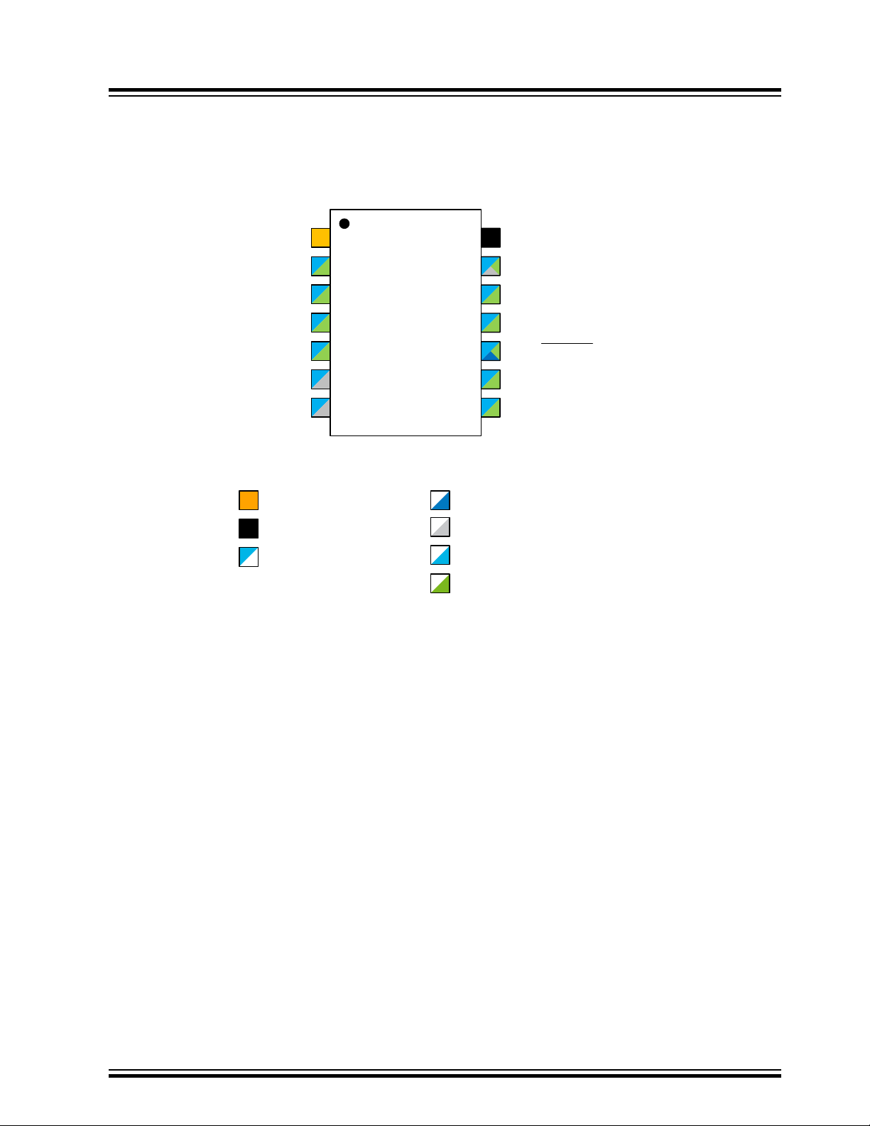
4. Pinout
4.1 14-Pin SOIC
ATtiny1614/1616/1617
Pinout
PA4
PA5
PA6
PA7
TOSC2/PB3
TOSC1/PB2
Ground
GPIO VDD power domain
1
2
3
4
5
14VDD GND
13
12
11
10
6
7 8
PA3/EXTCLK
PA2
PA1
PA0/RESET/UPDI
9
PB0
PB1
Programming, Debug, ResetInput supply
Clock, crystal
Digital function only
Analog function
© 2020 Microchip Technology Inc.
Complete Datasheet
DS40002204A-page 14
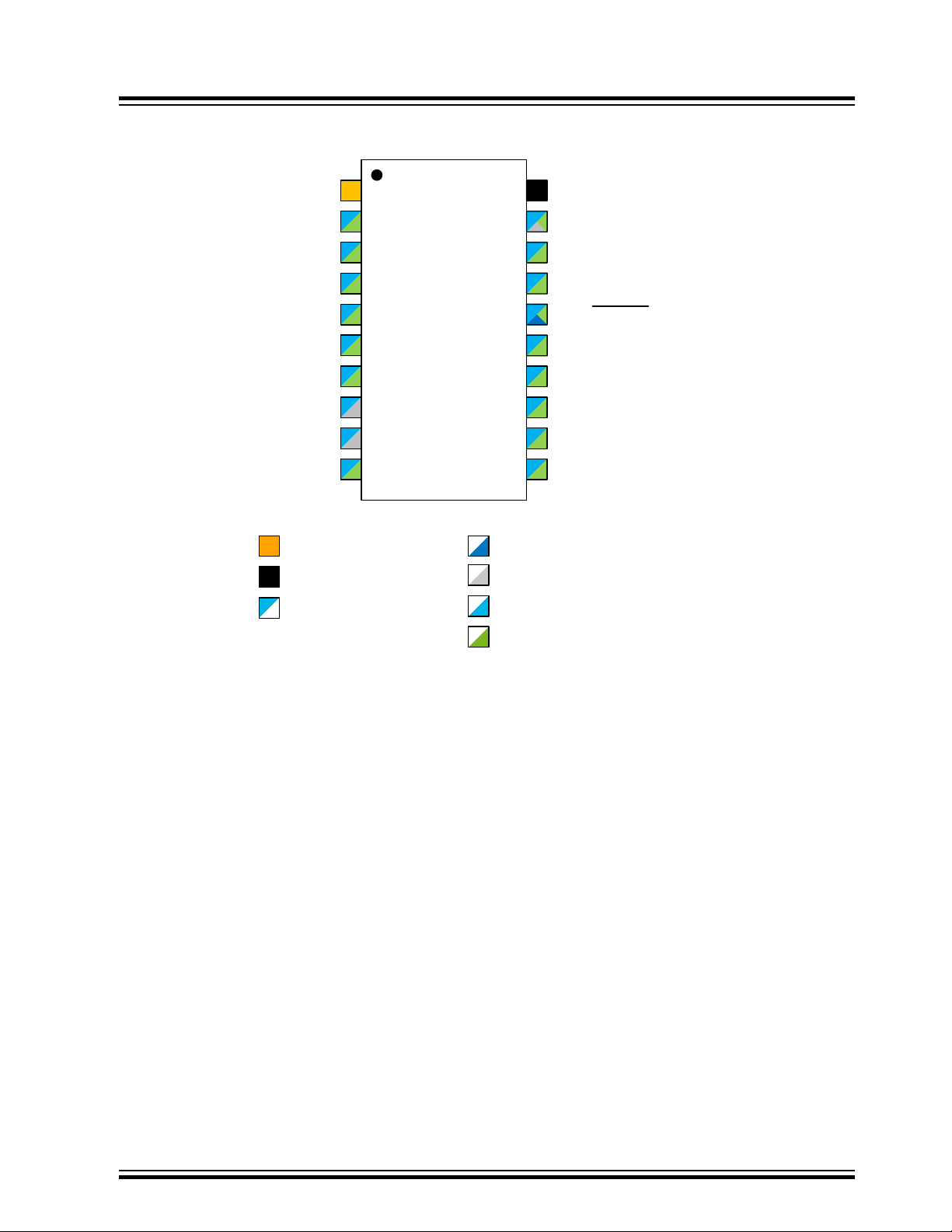
4.2 20-Pin SOIC
ATtiny1614/1616/1617
Pinout
TOSC1
TOSC2
V
DD
PA4
PA5
PA6
PA7
PB5
PB4
PB3
/
/PB2
PB1
Input supply
Ground
GPIO V
DD po
1
2
3
4
5
6
7
8
9
10
wer domain
20
19
18
17
16
15
14
13
12
11
Programming, Debug, Reset
Clock, crystal
Digital function only
Analog function
GND
PA3/EXTCLK
PA2
PA1
PA0/RESET/UPDI
PC3
PC2
PC1
PC0
PB0
© 2020 Microchip Technology Inc.
Complete Datasheet
DS40002204A-page 15
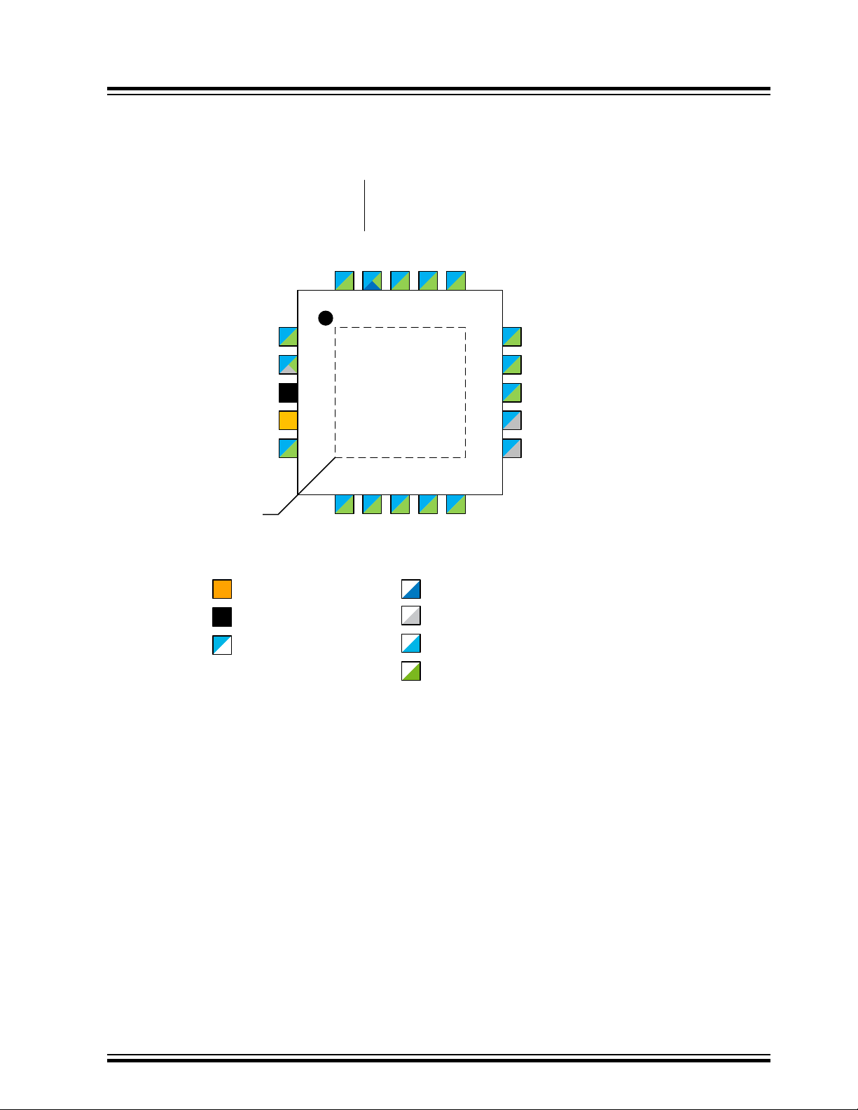
4.3 20-Pin VQFN
ATtiny1614/1616/1617
Pinout
UPDI
PA2 PC0
EXTCLK /PA3
GND
V
DD
PA4
Note: It is recommended to
solder the large center pad to
ground for mechanical stability
Ground
GPIO VDD power domain
PA0/RESET/
PA1
20
PC3
19
18
1
2
3
4
5
6
7
8
PC1
16
179
15
14
13
12
11
PB0
PB1
PB2/
PB3/
TOSC2
TOSC1
10
6
PB4
PA5
PA
PB5 PC2
PA7
Programming, Debug, ResetInput supply
Clock, crystal
Digital function only
© 2020 Microchip Technology Inc.
Analog function
Complete Datasheet
DS40002204A-page 16

4.4 24-Pin VQFN
ATtiny1614/1616/1617
Pinout
PA2
EXTCLK /PA3
GND
V
DD
PA4
PA5
Note: It is recommended to
solder the large center pad to
ground for mechanical stability
Ground
PA1
PA0/RESET/UPDI
PC5
PC4
23
22
24
21
1
2
3
4
5
6
7
8
9
10
PB7
PA7
PA6
PB6
Programming, Debug, ResetInput supply
Clock, crystal
PC2
PC3
20
19
18
17
16
15
14
13
12
11
PB5
PB4
PC1
PC0
PB0
PB1
PB2/
PB3/
TOSC2
TOSC1
GPIO VDD power domain
© 2020 Microchip Technology Inc.
Digital function only
Analog function
Complete Datasheet
DS40002204A-page 17

ATtiny1614/1616/1617
I/O Multiplexing and Considerations
5. I/O Multiplexing and Considerations
5.1 Multiplexed Signals
Table 5-1. PORT Function Multiplexing
(1,2)
Pin Name
SOIC 20-Pin
VQFN 24-Pin
23 19 16 10 PA0 RESET/ UPDI AIN0 LUT0-IN0
24 20 17 11 PA1 AIN1 TxD
1 1 18 12 PA2 EVOUT0 AIN2 RxD
2 2 19 13 PA3 EXTCLK AIN3 XCK
3 3 20 14 GND
4 4 1 1 V
5 5 2 2 PA4 AIN4 AIN0 X0/Y0 XDIR
6 6 3 3 PA5 VREFA AIN5 AIN1 X1/Y1 OUT AINN0 WO5 TCB0 WO WOB
7 7 4 4 PA6 AIN6 AIN2 X2/Y2 AINN0 AINP1 AINP0 OUT
8 8 5 5 PA7 AIN7 AIN3 X3/Y3 AINP0 AINP0 AINN0 LUT1-OUT
9 PB7 AIN4 AINN1 AINP3
10 PB6 AIN5 AINP3 AINN1
11 9 6 PB5 CLKOUT AIN8 X12/Y12 AINP1 AINP2 WO2
12 10 7 PB4 AIN9 X13/Y13 AINN1 AINP3 WO1
13 11 8 6 PB3 TOSC1 OUT RxD WO0
14 12 9 7 PB2 TOSC2, EVOUT1 OUT TxD WO2
15 13 10 8 PB1 AIN10 X4/Y4 AINP2 XCK SDA WO1
16 14 11 9 PB0 AIN11 X5/Y5 AINP2 AINP1 XDIR SCL WO0
17 15 12 PC0 AIN6 X6/Y6 SCK
18 16 13 PC1 AIN7 X7/Y7 MISO
19 17 14 PC2 EVOUT2 AIN8 X8/Y8 MOSI
20 18 15 PC3 AIN9 X9/Y9 SS
21 PC4 AIN10 X10/Y10 WO4
22 PC5 AIN11 X11/Y11 WO5
SOIC 14-Pin
VQFN 20-Pin
DD
Other/Special ADC0 ADC1 PTC
(4)
AC0 AC1 AC2 DAC0 USART0 SPI0 TWI0 TCA0 TCBn TCD0 CCL
(3)
MOSI SDA
(3)
MISO SCL
(3)
SCK WO3 TCB1 WO
(3)
SS WO4 WOA LUT0-OUT
(3)
(3)
(3)
(3)
(3)
(3)
(3)
(3)
(3)
(3)
WO3
(3)
(3)
TCB0 WO
TCB1 WO
(3)
(3)
LUT0-IN1
LUT0-IN2
LUT0-OUT
WOC
WOD LUT1-OUT
LUT1-IN0
LUT1-IN1
LUT1-IN2
(3)
(3)
Note:
1. Pin names are of type Pxn, with x being the PORT instance (A, B) and n the pin number. The notation for
signals is PORTx_PINn. All pins can be used as event input.
2. All pins can be used for external interrupt, where pins Px2 and Px6 of each port have full asynchronous
detection.
3. Alternate pin positions. For selecting the alternate positions, refer to section 15. PORTMUX - Port Multiplexer.
4. Every PTC line can be configured as X- or Y-line.
© 2020 Microchip Technology Inc.
Complete Datasheet
DS40002204A-page 18

6. Memories
6.1 Overview
The main memories are SRAM data memory, EEPROM data memory, and Flash program memory. Also, the
peripheral registers are located in the I/O memory space.
Table 6-1. Physical Properties of Flash Memory
Property
Size 16 KB
Page size 64B
Number of pages 256
Start address 0x8000
Table 6-2. Physical Properties of SRAM
Property
ATtiny1614/1616/1617
Memories
Size 2 KB
Start address 0x3800
Table 6-3. Physical Properties of EEPROM
Property
Size 256B
Page size 32B
Number of pages 8
Start address 0x1400
© 2020 Microchip Technology Inc.
Complete Datasheet
DS40002204A-page 19
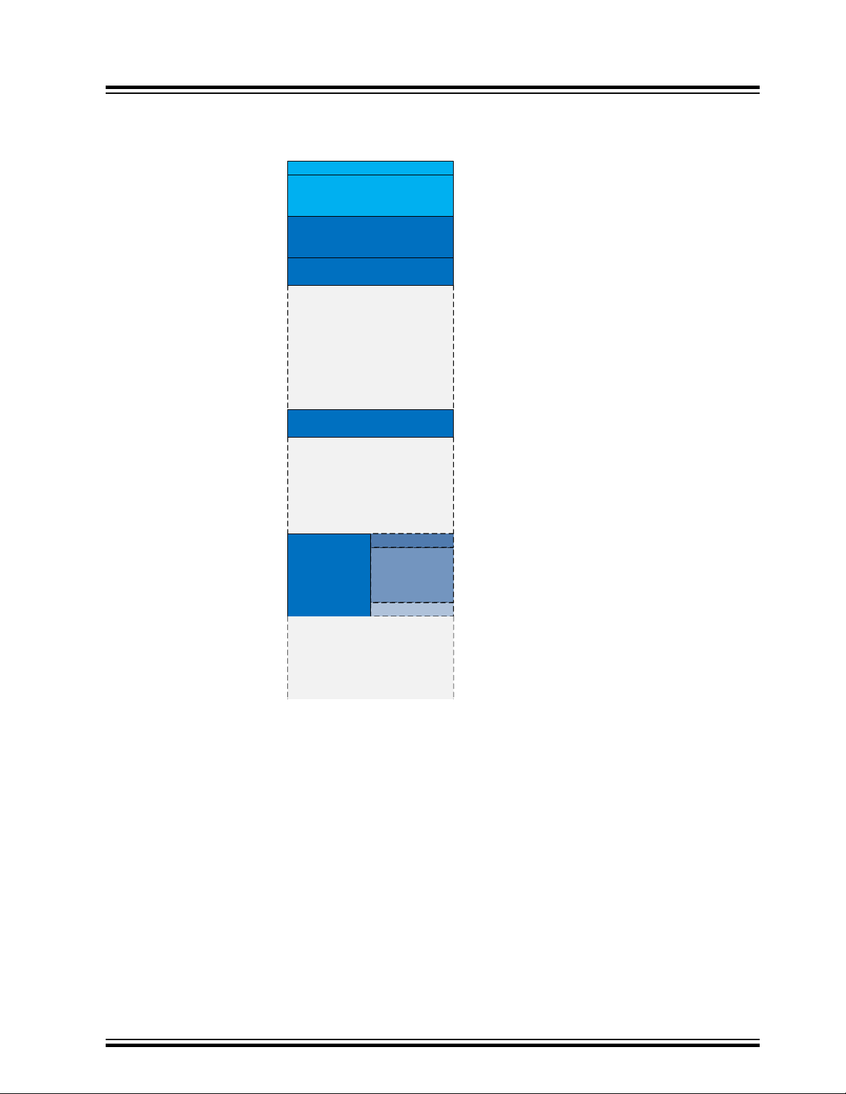
6.2 Memory Map
(Reserved)
(Reserved)
NVM I/O Registers and Data
64 I/O Registers
960 Ext. I/O Registers
0x0000 – 0x003F
0x0040 – 0x0FFF
Internal SRAM
2 KB
EEPROM 256 bytes
0x8000 -
BOOTEND
0x1000 – 0x13FF
0x3800 –
0x3FFF
0x1400 – 0x14FF
0xBFFF
Application
Code
App. Data
APPEND
Flash
16 KB
(Reserved)
Boot
0xFFFF
Figure 6-1. Memory Map
ATtiny1614/1616/1617
Memories
6.3 In-System Reprogrammable Flash Program Memory
The ATtiny1614/1616/1617 contains 16 KB on-chip in-system reprogrammable Flash memory for program storage.
Since all AVR instructions are 16 or 32-bit wide, the Flash is organized as 4K x 16. For write protection, the Flash
program memory space can be divided into three sections (see the illustration below): Bootloader section, Application
code section, and Application data section, with restricted access rights among them.
The Program Counter (PC) is 13-bit wide to address the whole program memory. The procedure for writing Flash
memory is described in detail in the documentation of the Nonvolatile Memory Controller (NVMCTRL) peripheral.
The entire Flash memory is mapped in the memory space and is accessible with normal LD/ST instructions as well as
the LPM instruction. For LD/ST instructions, the Flash is mapped from address 0x8000. For the LPM instruction, the
Flash start address is 0x0000.
The ATtiny1614/1616/1617 also has a CRC peripheral that is a master on the bus.
© 2020 Microchip Technology Inc.
Complete Datasheet
DS40002204A-page 20

Figure 6-2. Flash and the Three Sections
FLASHSTART: 0x8000
BOOTEND>0: 0x8000+BOOTEND*256
BO O T
APPEND>0: 0x8000+APPEND*256
AP PL IC A T IO N
CO DE
AP PL IC A T IO N
DA TA
FLASH
FLASHEND
ATtiny1614/1616/1617
Memories
6.4 SRAM Data Memory
The 2 KB SRAM is used for data storage and stack.
6.5 EEPROM Data Memory
The ATtiny1614/1616/1617 has 256 bytes of EEPROM data memory, see section 6.2 Memory Map. The EEPROM
memory supports single-byte read and write. The EEPROM is controlled by the Nonvolatile Memory Controller
(NVMCTRL).
6.6 User Row
In addition to the EEPROM, the ATtiny1614/1616/1617 has one extra page of EEPROM memory that can be used for
firmware settings; the User Row (USERROW). This memory supports single-byte read and write as the normal
EEPROM. The CPU can write and read this memory as normal EEPROM, and the UPDI can write and read it as a
normal EEPROM memory if the part is unlocked. The User Row can be written by the UPDI when the part is locked.
USERROW is not affected by a chip erase.
6.7 Signature Bytes
All tinyAVR® microcontrollers have a 3-byte signature code that identifies the device. The three bytes reside in a
separate address space. For the device, the signature bytes are given in the following table.
Note: When the device is locked, only the System Information Block (SIB) can be accessed.
Table 6-4. Device ID
Device Name Signature Bytes Address
ATtiny1614 0x1E 0x94 0x22
ATtiny1616 0x1E 0x94 0x21
0x00 0x01 0x02
© 2020 Microchip Technology Inc.
Complete Datasheet
DS40002204A-page 21

...........continued
Device Name Signature Bytes Address
ATtiny1617 0x1E 0x94 0x20
6.8 I/O Memory
All ATtiny1614/1616/1617 I/Os and peripherals are located in the I/O memory space. The I/O address range from
0x00 to 0x3F can be accessed in a single cycle using IN and OUT instructions. The extended I/O memory space from
0x0040 to 0x0FFF can be accessed by the LD/LDS/LDD and ST/STS/STD instructions, transferring data between the
32 general purpose working registers and the I/O memory space.
I/O registers within the address range 0x00-0x1F are directly bit-accessible using the SBI and CBI instructions. In
these registers, the value of single bits can be checked by using the SBIS and SBIC instructions. Refer to the
Instruction Set section for more details.
For compatibility with future devices, reserved bits must be written to ‘0’, if accessed. Reserved I/O memory
addresses must never be written.
Some of the interrupt flags are cleared by writing a ‘1’ to them. On ATtiny1614/1616/1617 devices, the CBI and SBI
instructions will only operate on the specified bit and can be used on registers containing such interrupt flags. The
CBI and SBI instructions work with registers 0x00-0x1F only.
ATtiny1614/1616/1617
Memories
0x00 0x01 0x02
General Purpose I/O Registers
The ATtiny1614/1616/1617 devices provide four general purpose I/O registers. These registers can be used for
storing any information, and they are particularly useful for storing global variables and interrupt flags. General
purpose I/O registers, which reside in the address range 0x1C-0x1F, are directly bit-accessible using the SBI, CBI,
SBIS, and SBIC instructions.
© 2020 Microchip Technology Inc.
Complete Datasheet
DS40002204A-page 22

ATtiny1614/1616/1617
Memories
6.8.1 Register Summary
Offset Name Bit Pos. 7 6 5 4 3 2 1 0
0x00 GPIOR0 7:0 GPIOR[7:0]
0x01 GPIOR1 7:0 GPIOR[7:0]
0x02 GPIOR2 7:0 GPIOR[7:0]
0x03 GPIOR3 7:0 GPIOR[7:0]
6.8.2 Register Description
© 2020 Microchip Technology Inc.
Complete Datasheet
DS40002204A-page 23

ATtiny1614/1616/1617
Memories
6.8.2.1 General Purpose I/O Register n
Name: GPIORn
Offset: 0x00 + n*0x01 [n=0..3]
Reset: 0x00
Property: -
These are general purpose registers that can be used to store data, such as global variables and flags, in the bitaccessible I/O memory space.
Bit 7 6 5 4 3 2 1 0
Access
Reset 0 0 0 0 0 0 0 0
R/W R/W R/W R/W R/W R/W R/W R/W
Bits 7:0 – GPIOR[7:0] General Purpose I/O Register Byte
6.9 Memory Section Access from CPU and UPDI on Locked Device
The device can be locked so that the memories cannot be read using the UPDI. The locking protects both the Flash
(all Boot, Application Code, and Application Date sections), SRAM, and the EEPROM including the FUSE data. This
prevents successful reading of application data or code using the debugger interface. Regular memory access from
within the application is still enabled.
The device is locked by writing a non-valid key to the LOCKBIT bit field in FUSE.LOCKBIT.
Table 6-5. Memory Access Unlocked (FUSE.LOCKBIT Valid Key)
GPIOR[7:0]
(1)
Memory Section CPU Access UPDI Access
Read Write Read Write
SRAM Yes Yes Yes Yes
Registers Yes Yes Yes Yes
Flash Yes Yes Yes Yes
EEPROM Yes Yes Yes Yes
USERROW Yes Yes Yes Yes
SIGROW Yes No Yes No
Other fuses Yes No Yes Yes
Table 6-6. Memory Access Locked (FUSE.LOCKBIT Invalid Key)
(1)
Memory Section CPU Access UPDI Access
Read Write Read Write
SRAM Yes Yes No No
Registers Yes Yes No No
Flash Yes Yes No No
EEPROM Yes Yes No No
USERROW Yes Yes No Yes
(2)
SIGROW Yes No No No
Other fuses Yes No No No
© 2020 Microchip Technology Inc.
Complete Datasheet
DS40002204A-page 24

Note:
1. Read operations marked No in the tables may appear to be successful, but the data are not valid. Hence, any
attempt of code validation through the UPDI will fail on these memory sections.
2. In the Locked mode, the USERROW can be written using the Fuse Write command, but the current
USERROW values cannot be read out.
Important: The only way to unlock a device is through a CHIPERASE. No application data are retained.
6.10 Configuration and User Fuses (FUSE)
Fuses are part of the nonvolatile memory and hold the device configuration. The fuses are available from the device
power-up. The fuses can be read by the CPU or the UPDI, but can only be programmed or cleared by the UPDI. The
configuration values stored in the fuses are written to their respective target registers at the end of the start-up
sequence.
The fuses for peripheral configuration (FUSE) are pre-programmed but can be altered by the user. Altered values in
the configuration fuse will be effective only after a Reset.
Note: When writing the fuses, all reserved bits must be written to ‘1’.
ATtiny1614/1616/1617
Memories
© 2020 Microchip Technology Inc.
Complete Datasheet
DS40002204A-page 25

ATtiny1614/1616/1617
Memories
6.10.1 Signature Row Summary
Offset Name Bit Pos. 7 6 5 4 3 2 1 0
0x00 DEVICEID0 7:0 DEVICEID[7:0]
0x01 DEVICEID1 7:0 DEVICEID[7:0]
0x02 DEVICEID2 7:0 DEVICEID[7:0]
0x03 SERNUM0 7:0 SERNUM[7:0]
0x04 SERNUM1 7:0 SERNUM[7:0]
0x05 SERNUM2 7:0 SERNUM[7:0]
0x06 SERNUM3 7:0 SERNUM[7:0]
0x07 SERNUM4 7:0 SERNUM[7:0]
0x08 SERNUM5 7:0 SERNUM[7:0]
0x09 SERNUM6 7:0 SERNUM[7:0]
0x0A SERNUM7 7:0 SERNUM[7:0]
0x0B SERNUM8 7:0 SERNUM[7:0]
0x0C SERNUM9 7:0 SERNUM[7:0]
0x0D
...
0x1F
0x20 TEMPSENSE0 7:0 TEMPSENSE[7:0]
0x21 TEMPSENSE1 7:0 TEMPSENSE[7:0]
0x22 OSC16ERR3V 7:0 OSC16ERR3V[7:0]
0x23 OSC16ERR5V 7:0 OSC16ERR5V[7:0]
0x24 OSC20ERR3V 7:0 OSC20ERR3V[7:0]
0x25 OSC20ERR5V 7:0 OSC20ERR5V[7:0]
Reserved
6.10.2 Signature Row Description
© 2020 Microchip Technology Inc.
Complete Datasheet
DS40002204A-page 26

ATtiny1614/1616/1617
Memories
6.10.2.1 Device ID n
Name: DEVICEIDn
Offset: 0x00 + n*0x01 [n=0..2]
Reset: [Device ID]
Property: -
Each device has a device ID identifying this device and its properties such as memory sizes, pin count, and die
revision. This can be used to identify a device and hence, the available features by software. The Device ID consists
of three bytes: SIGROW.DEVICEID[2:0].
Bit 7 6 5 4 3 2 1 0
Access
Reset x x x x x x x x
R R R R R R R R
Bits 7:0 – DEVICEID[7:0] Byte n of the Device ID
DEVICEID[7:0]
© 2020 Microchip Technology Inc.
Complete Datasheet
DS40002204A-page 27

ATtiny1614/1616/1617
Memories
6.10.2.2 Serial Number Byte n
Name: SERNUMn
Offset: 0x03 + n*0x01 [n=0..9]
Reset: [device serial number]
Property: -
Each device has an individual serial number, representing a unique ID. This can be used to identify a specific device
in the field. The serial number consists of ten bytes: SIGROW.SERNUM[9:0].
Bit 7 6 5 4 3 2 1 0
Access
Reset x x x x x x x x
R R R R R R R R
Bits 7:0 – SERNUM[7:0] Serial Number Byte n
SERNUM[7:0]
© 2020 Microchip Technology Inc.
Complete Datasheet
DS40002204A-page 28

ATtiny1614/1616/1617
Memories
6.10.2.3 Temperature Sensor Calibration n
Name: TEMPSENSEn
Offset: 0x20 + n*0x01 [n=0..1]
Reset: [Temperature sensor calibration value]
Property: -
The Temperature Sensor Calibration registers contain correction factors for temperature measurements from the onchip sensor. The ADC.SIGROW.TEMPSENSE0 is a correction factor for the gain/slope (unsigned), and
SIGROW.TEMPSENSE1 is a correction factor for the offset (signed).
Bit 7 6 5 4 3 2 1 0
Access
Reset x x x x x x x x
R R R R R R R R
Bits 7:0 – TEMPSENSE[7:0] Temperature Sensor Calibration Byte n
Refer to the ADC section for a description of how to use this register.
TEMPSENSE[7:0]
© 2020 Microchip Technology Inc.
Complete Datasheet
DS40002204A-page 29

ATtiny1614/1616/1617
Memories
6.10.2.4 OSC16 Error at 3V
Name: OSC16ERR3V
Offset: 0x22
Reset: [Oscillator frequency error value]
Property: -
Bit 7 6 5 4 3 2 1 0
Access
Reset x x x x x x x x
R R R R R R R R
Bits 7:0 – OSC16ERR3V[7:0] OSC16 Error at 3V
These registers contain the signed oscillator frequency error value relative to the nominal oscillator frequency when
running at an internal 16 MHz at 3V, as measured during production.
OSC16ERR3V[7:0]
© 2020 Microchip Technology Inc.
Complete Datasheet
DS40002204A-page 30

ATtiny1614/1616/1617
Memories
6.10.2.5 OSC16 Error at 5V
Name: OSC16ERR5V
Offset: 0x23
Reset: [Oscillator frequency error value]
Property: -
Bit 7 6 5 4 3 2 1 0
Access
Reset x x x x x x x x
R R R R R R R R
Bits 7:0 – OSC16ERR5V[7:0] OSC16 Error at 5V
These registers contain the signed oscillator frequency error value relative to the nominal oscillator frequency when
running at an internal 16 MHz at 5V, as measured during production.
OSC16ERR5V[7:0]
© 2020 Microchip Technology Inc.
Complete Datasheet
DS40002204A-page 31

ATtiny1614/1616/1617
Memories
6.10.2.6 OSC20 Error at 3V
Name: OSC20ERR3V
Offset: 0x24
Reset: [Oscillator frequency error value]
Property: -
Bit 7 6 5 4 3 2 1 0
Access
Reset x x x x x x x x
R R R R R R R R
Bits 7:0 – OSC20ERR3V[7:0] OSC20 Error at 3V
These registers contain the signed oscillator frequency error value relative to the nominal oscillator frequency when
running at an internal 20 MHz at 3V, as measured during production.
OSC20ERR3V[7:0]
© 2020 Microchip Technology Inc.
Complete Datasheet
DS40002204A-page 32

ATtiny1614/1616/1617
Memories
6.10.2.7 OSC20 Error at 5V
Name: OSC20ERR5V
Offset: 0x25
Reset: [Oscillator frequency error value]
Property: -
Bit 7 6 5 4 3 2 1 0
Access
Reset x x x x x x x x
R R R R R R R R
Bits 7:0 – OSC20ERR5V[7:0] OSC20 Error at 5V
These registers contain the signed oscillator frequency error value relative to the nominal oscillator frequency when
running at an internal 20 MHz at 5V, as measured during production.
OSC20ERR5V[7:0]
© 2020 Microchip Technology Inc.
Complete Datasheet
DS40002204A-page 33

ATtiny1614/1616/1617
Memories
6.10.3 Fuse Summary - FUSE
Offset Name Bit Pos. 7 6 5 4 3 2 1 0
0x00 WDTCFG 7:0 WINDOW[3:0] PERIOD[3:0]
0x01 BODCFG 7:0 LVL[2:0] SAMPFREQ ACTIVE[1:0] SLEEP[1:0]
0x02 OSCCFG 7:0 OSCLOCK FREQSEL[1:0]
0x03 Reserved
0x04 TCD0CFG 7:0 CMPDEN CMPCEN CMPBEN CMPAEN CMPD CMPC CMPB CMPA
0x05 SYSCFG0 7:0 CRCSRC[1:0] RSTPINCFG[1:0] EESAVE
0x06 SYSCFG1 7:0 SUT[2:0]
0x07 APPEND 7:0 APPEND[7:0]
0x08 BOOTEND 7:0 BOOTEND[7:0]
0x09 Reserved
0x0A LOCKBIT 7:0 LOCKBIT[7:0]
6.10.4 Fuse Description
© 2020 Microchip Technology Inc.
Complete Datasheet
DS40002204A-page 34

ATtiny1614/1616/1617
Memories
6.10.4.1 Watchdog Configuration
Name: WDTCFG
Offset: 0x00
Reset: Property: -
Bit 7 6 5 4 3 2 1 0
Access
Reset 0 0 0 0 0 0 0 0
R R R R R R R R
Bits 7:4 – WINDOW[3:0] Watchdog Window Time-Out Period
This value is loaded into the WINDOW bit field of the Watchdog Control A (WDT.CTRLA) register during Reset.
Bits 3:0 – PERIOD[3:0] Watchdog Time-Out Period
This value is loaded into the PERIOD bit field of the Watchdog Control A (WDT.CTRLA) register during Reset.
WINDOW[3:0] PERIOD[3:0]
© 2020 Microchip Technology Inc.
Complete Datasheet
DS40002204A-page 35

ATtiny1614/1616/1617
Memories
6.10.4.2 BOD Configuration
Name: BODCFG
Offset: 0x01
Reset: Property: -
The bit values of this fuse register are written to the corresponding BOD configuration registers at start-up.
Bit 7 6 5 4 3 2 1 0
Access
Reset 0 0 0 0 0 0 0 0
R R R R R R R R
Bits 7:5 – LVL[2:0] BOD Level
This value is loaded into the LVL bit field of the BOD Control B (BOD.CTRLB) register during Reset.
Value Name Description
0x0
0x2
0x7
Note:
• The values in the description are typical
• Refer to the BOD and POR Characteristics in Electrical Characteristics for maximum and minimum values
LVL[2:0] SAMPFREQ ACTIVE[1:0] SLEEP[1:0]
BODLEVEL0 1.8V
BODLEVEL2 2.6V
BODLEVEL7 4.2V
Bit 4 – SAMPFREQ BOD Sample Frequency
This value is loaded into the SAMPFREQ bit of the BOD Control A (BOD.CTRLA) register during Reset.
Value Description
0x0
0x1
Bits 3:2 – ACTIVE[1:0] BOD Operation Mode in Active and Idle
This value is loaded into the ACTIVE bit field of the BOD Control A (BOD.CTRLA) register during Reset.
Value Description
0x0
0x1
0x2
0x3
Bits 1:0 – SLEEP[1:0] BOD Operation Mode in Sleep
This value is loaded into the SLEEP bit field of the BOD Control A (BOD.CTRLA) register during Reset.
Value Description
0x0
0x1
0x2
0x3
Sample frequency is 1 kHz
Sample frequency is 125 Hz
Disabled
Enabled
Sampled
Enabled with wake-up halted until BOD is ready
Disabled
Enabled
Sampled
Reserved
© 2020 Microchip Technology Inc.
Complete Datasheet
DS40002204A-page 36

ATtiny1614/1616/1617
Memories
6.10.4.3 Oscillator Configuration
Name: OSCCFG
Offset: 0x02
Reset: Property: -
Bit 7 6 5 4 3 2 1 0
OSCLOCK FREQSEL[1:0]
Access
Reset 0 1 0
R R R
Bit 7 – OSCLOCK Oscillator Lock
This Fuse bit is loaded to LOCK in CLKCTRL.OSC20MCALIBB during Reset.
Value Description
0
1
Bits 1:0 – FREQSEL[1:0] Frequency Select
This bit field selects the operation frequency of the 16/20 MHz internal oscillator (OSC20M) and determines the
respective factory calibration values to be written to CAL20M in CLKCTRL.OSC20MCALIBA and TEMPCAL20M in
CLKCTRL.OSC20MCALIBB.
Value Description
0x1
0x2
Other
Calibration registers of the OSC20M oscillator are accessible
Calibration registers of the OSC20M oscillator are locked
Run at 16 MHz with corresponding factory calibration
Run at 20 MHz with corresponding factory calibration
Reserved
© 2020 Microchip Technology Inc.
Complete Datasheet
DS40002204A-page 37

ATtiny1614/1616/1617
Memories
6.10.4.4 Timer Counter Type D Configuration
Name: TCD0CFG
Offset: 0x04
Reset: Property: -
The bit values of this fuse register are written to the corresponding bits in the TCD.FAULTCTRL register of TCD0 at
start-up.
Bit 7 6 5 4 3 2 1 0
CMPDEN CMPCEN CMPBEN CMPAEN CMPD CMPC CMPB CMPA
Access
Reset 0 0 0 0 0 0 0 0
R R R R R R R R
Bits 4, 5, 6, 7 – CMPEN Compare x Enable
Value Description
0
1
Bits 0, 1, 2, 3 – CMP Compare x
This bit selects the default state of Compare x after Reset, or when entering debug if FAULTDET is '1'.
Value Description
0
1
Compare x output on Pin is disabled
Compare x output on Pin is enabled
Compare x default state is ‘0’
Compare x default state is ‘1’
© 2020 Microchip Technology Inc.
Complete Datasheet
DS40002204A-page 38

ATtiny1614/1616/1617
Memories
6.10.4.5 System Configuration 0
Name: SYSCFG0
Offset: 0x05
Reset: 0xC4
Property: -
Bit 7 6 5 4 3 2 1 0
Access
Reset 1 1 0 1 0
Bits 7:6 – CRCSRC[1:0] CRC Source
See the CRC description for more information about the functionality.
Value Name Description
0x0
0x1
0x2
0x3
Bits 3:2 – RSTPINCFG[1:0] Reset Pin Configuration
This bit field selects the Reset/UPDI pin configuration.
Value Description
0x0
0x1
0x2
Other
CRCSRC[1:0] RSTPINCFG[1:0] EESAVE
R R R R R
FLASH CRC of full Flash (boot, application code and application data)
BOOT CRC of the boot section
BOOTAPP CRC of application code and boot sections
NOCRC No CRC
GPIO
UPDI
RESET
Reserved
Note: When configuring the RESET pin as GPIO, there is a potential conflict between the GPIO actively driving the
output, and a high-voltage UPDI enable sequence initiation. To avoid this, the GPIO output driver is disabled for 768
OSC32K cycles after a System Reset. Enable any interrupts for this pin only after this period.
Bit 0 – EESAVE EEPROM Save During Chip Erase
Note: If the device is locked, the EEPROM is always erased by a chip erase, regardless of this bit.
Value Description
0
1
EEPROM erased during chip erase
EEPROM not erased under chip erase
© 2020 Microchip Technology Inc.
Complete Datasheet
DS40002204A-page 39

ATtiny1614/1616/1617
Memories
6.10.4.6 System Configuration 1
Name: SYSCFG1
Offset: 0x06
Reset: Property: -
Bit 7 6 5 4 3 2 1 0
Access
Reset 1 1 1
SUT[2:0]
R R R
Bits 2:0 – SUT[2:0] Start-Up Time Setting
This bit field selects the start-up time between power-on and code execution.
Value Description
0x0
0x1
0x2
0x3
0x4
0x5
0x6
0x7
0 ms
1 ms
2 ms
4 ms
8 ms
16 ms
32 ms
64 ms
© 2020 Microchip Technology Inc.
Complete Datasheet
DS40002204A-page 40

ATtiny1614/1616/1617
Memories
6.10.4.7 Application Code End
Name: APPEND
Offset: 0x07
Reset: Property: -
Bit 7 6 5 4 3 2 1 0
Access
Reset 0 0 0 0 0 0 0 0
R R R R R R R R
Bits 7:0 – APPEND[7:0] Application Code Section End
This bit field sets the end of the application code section in blocks of 256 bytes. The end of the application code
section will be set as (BOOT size) + (application code size). The remaining Flash will be application data. A value of
0x00 defines the Flash from BOOTEND*256 to the end of Flash as the application code. When both FUSE.APPEND
and FUSE.BOOTEND are 0x00, the entire Flash is the BOOT section.
APPEND[7:0]
© 2020 Microchip Technology Inc.
Complete Datasheet
DS40002204A-page 41

ATtiny1614/1616/1617
Memories
6.10.4.8 Boot End
Name: BOOTEND
Offset: 0x08
Reset: Property: -
Bit 7 6 5 4 3 2 1 0
Access
Reset 0 0 0 0 0 0 0 0
R R R R R R R R
Bits 7:0 – BOOTEND[7:0] Boot Section End
This bit field sets the end of the boot section in blocks of 256 bytes. A value of 0x00 defines the whole Flash as the
BOOT section. When both FUSE.APPEND and FUSE.BOOTEND are 0x00, the entire Flash is the BOOT section.
BOOTEND[7:0]
© 2020 Microchip Technology Inc.
Complete Datasheet
DS40002204A-page 42

ATtiny1614/1616/1617
Memories
6.10.4.9 Lockbits
Name: LOCKBIT
Offset: 0x0A
Reset: Property: -
Bit 7 6 5 4 3 2 1 0
Access
Reset 0 0 0 0 0 0 0 0
R/W R/W R/W R/W R/W R/W R/W R/W
Bits 7:0 – LOCKBIT[7:0] Lockbits
When the part is locked, UPDI cannot access the system bus, so it cannot read out anything but the System
Information Block (SIB).
Value Description
0xC5
other
Valid key - memory access is unlocked
Invalid key - memory access is locked
LOCKBIT[7:0]
© 2020 Microchip Technology Inc.
Complete Datasheet
DS40002204A-page 43

7. Peripherals and Architecture
7.1 Peripheral Address Map
The address map shows the base address for each peripheral. For complete register description and summary for
each peripheral, refer to the respective sections.
Table 7-1. Peripheral Address Map
Base Address Name Description
0x0000 VPORTA Virtual Port A
0x0004 VPORTB Virtual Port B
0x0008 VPORTC Virtual Port C
0x001C GPIO General Purpose I/O registers
0x0030 CPU CPU
0x0040 RSTCTRL Reset Controller
ATtiny1614/1616/1617
Peripherals and Architecture
(1)
0x0050 SLPCTRL Sleep Controller
0x0060 CLKCTRL Clock Controller
0x0080 BOD Brown-out Detector
0x00A0 VREF Voltage Reference
0x0100 WDT Watchdog Timer
0x0110 CPUINT Interrupt Controller
0x0120 CRCSCAN Cyclic Redundancy Check Memory Scan
0x0140 RTC Real-Time Counter
0x0180 EVSYS Event System
0x01C0 CCL Configurable Custom Logic
0x0200 PORTMUX Port Multiplexer
0x0400 PORTA Port A Configuration
0x0420 PORTB Port B Configuration
0x0440 PORTC Port C Configuration
0x0600 ADC0 Analog-to-Digital Converter 0/Peripheral Touch Controller
0x0640 ADC1 Analog-to-Digital Converter 1
0x0680 AC0 Analog Comparator 0
(1)
0x0688 AC1 Analog Comparator 1
0x0690 AC2 Analog Comparator 2
0x06A0 DAC0 Digital-to-Analog Converter 0
0x06A8 DAC1 Digital-to-Analog Converter 1
0x06B0 DAC2 Digital-to-Analog Converter 2
0x0800 USART0 Universal Synchronous Asynchronous Receiver Transmitter 0
© 2020 Microchip Technology Inc.
Complete Datasheet
DS40002204A-page 44

ATtiny1614/1616/1617
Peripherals and Architecture
...........continued
Base Address Name Description
0x0810 TWI0 Two-Wire Interface 0
0x0820 SPI0 Serial Peripheral Interface 0
0x0A00 TCA0 Timer/Counter Type A 0
0x0A40 TCB0 Timer/Counter Type B 0
0x0A50 TCB1 Timer/Counter Type B 1
0x0A80 TCD0 Timer/Counter Type D 0
0x0F00 SYSCFG System Configuration
0x1000 NVMCTRL Nonvolatile Memory Controller
0x1100 SIGROW Signature Row
0x1280 FUSES Device-specific fuses
0x1300 USERROW User Row
Note:
1. The availability of this register depends on the device pin count. PORTC/VPORTC is available for devices with
20 pins or more.
7.2 Interrupt Vector Mapping
Each of the interrupt vectors is connected to one peripheral instance, as shown in the table below. A peripheral can
have one or more interrupt sources, see the Interrupt section in the Functional Description of the respective
peripheral for more details on the available interrupt sources.
When the Interrupt condition occurs, an Interrupt flag (nameIF) is set in the Interrupt Flags register of the peripheral
(peripheral.INTFLAGS).
An interrupt is enabled or disabled by writing to the corresponding Interrupt Enable (nameIE) bit in the peripheral's
Interrupt Control (peripheral.INTCTRL) register.
The naming of the registers may vary slightly in some peripherals.
An interrupt request is generated when the corresponding interrupt is enabled, and the interrupt flag is set. The
interrupt request remains Active until the Interrupt flag is cleared. See the peripheral's INTFLAGS register for details
on how to clear interrupt flags.
Interrupts must be enabled globally for interrupt requests to be generated.
Table 7-2. Interrupt Vector Mapping
Vector Number Program Address
(word)
0 0x00 RESET RESET
1 0x02 CRCSCAN_NMI NMI - Non-Maskable Interrupt from CRC
2 0x04 BOD_VLM VLM - Voltage Level Monitor
3 0x06 PORTA_PORT PORTA - Port A
Peripheral Source Description
4 0x08 PORTB_PORT PORTB - Port B
5 0x0A PORTC_PORT PORTC - Port C
6 0x0C RTC_CNT RTC - Real-Time Counter
© 2020 Microchip Technology Inc.
Complete Datasheet
(1)
DS40002204A-page 45

ATtiny1614/1616/1617
Peripherals and Architecture
...........continued
Vector Number Program Address
(word)
7 0x0E RTC_PIT PIT - Periodic Interrupt Timer (in RTC
8 0x10 TCA0_LUNF/TCA0_OVF TCA0 - Timer Counter Type A, LUNF/OVF
9 0x12 TCA0_HUNF TCA0, HUNF
Peripheral Source Description
peripheral)
10 0x14 TCA0_LCMP0/
TCA0_CMP0
11 0x16 TCA0_LCMP1/
TCA0_CMP1
12 0x18 TCA0_CMP2/
TCA0_LCMP2
13 0x1A TCB0_INT TCB0 - Timer Counter Type B
14 0x1C TCB1_INT TCB1 - Timer Counter Type B
15 0x1E TCD0_OVF TCD0 - Timer Counter Type D, OVF
16 0x20 TCD0_TRIG TCD0, TRIG
17 0x22 AC0_AC AC0 – Analog Comparator
18 0x24 AC1_AC AC1 – Analog Comparator
19 0x26 AC2_AC AC2 – Analog Comparator
20 0x28 ADC0_RESRDY ADC0 – Analog-to-Digital Converter, RESRDY
21 0x2A ADC0_WCOMP ADC0, WCOMP
22 0x2C ADC1_RESRDY ADC1 – Analog-to-Digital Converter, RESRDY
23 0x2E ADC1_WCOMP ADC1, WCOMP
24 0x30 TWI0_TWIS TWI0 - Two-Wire Interface/I2C, TWIS
TCA0, LCMP0/CMP0
TCA0, LCMP1/CMP1
TCA0, LCMP2/CMP2
25 0x32 TWI0_TWIM TWI0, TWIM
26 0x34 SPI0_INT SPI0 - Serial Peripheral Interface
27 0x36 USART0_RXC USART0 - Universal Asynchronous Receiver-
28 0x38 USART0_DRE USART0, DRE
29 0x3A USART0_TXC USART0, TXC
30 0x3C NVMCTRL_EE NVM - Nonvolatile Memory
Note:
1. The availability of the port pins depends on the device pin count. PORTC is available for devices with 20 pins
or more.
7.3 System Configuration (SYSCFG)
The system configuration contains the revision ID of the part. The revision ID is readable from the CPU, making it
useful for implementing application changes between part revisions.
© 2020 Microchip Technology Inc.
Transmitter, RXC
Complete Datasheet
DS40002204A-page 46

ATtiny1614/1616/1617
Peripherals and Architecture
7.3.1 Register Summary
Offset Name Bit Pos. 7 6 5 4 3 2 1 0
0x00 Reserved
0x01 REVID 7:0 REVID[7:0]
7.3.2 Register Description
© 2020 Microchip Technology Inc.
Complete Datasheet
DS40002204A-page 47

ATtiny1614/1616/1617
Peripherals and Architecture
7.3.2.1 Device Revision ID Register
Name: REVID
Offset: 0x01
Reset: [revision ID]
Property: -
This register is read-only and displays the device revision ID.
Bit 7 6 5 4 3 2 1 0
Access
Reset
R R R R R R R R
Bits 7:0 – REVID[7:0] Revision ID
This bit field contains the device revision. 0x00 = A, 0x01 = B, and so on.
REVID[7:0]
© 2020 Microchip Technology Inc.
Complete Datasheet
DS40002204A-page 48

8. AVR® CPU
8.1 Features
• 8-bit, High-Performance AVR RISC CPU:
– 135 instructions
– Hardware multiplier
• 32 8-bit Registers Directly Connected to the ALU
• Stack in RAM
• Stack Pointer Accessible in I/O Memory Space
• Direct Addressing of up to 64 KB of Unified Memory
• Efficient Support for 8-, 16-, and 32-bit Arithmetic
• Configuration Change Protection for System-Critical Features
• Native On-Chip Debugging (OCD) Support:
– Two hardware breakpoints
– Change of flow, interrupt, and software breakpoints
– Run-time read-out of Stack Pointer (SP) register, Program Counter (PC), and Status Register (SREG)
– Register file read- and writable in Stopped mode
ATtiny1614/1616/1617
AVR® CPU
8.2 Overview
All AVR devices use the AVR 8-bit CPU. The CPU is able to access memories, perform calculations, control
peripherals, and execute instructions in the program memory. Interrupt handling is described in a separate section.
8.3 Architecture
To maximize performance and parallelism, the AVR CPU uses a Harvard architecture with separate buses for
program and data. Instructions in the program memory are executed with a single-level pipeline. While one
instruction is being executed, the next instruction is pre-fetched from the program memory. This enables instructions
to be executed on every clock cycle.
Refer to the Instruction Set Summary section for a summary of all AVR instructions.
© 2020 Microchip Technology Inc.
Complete Datasheet
DS40002204A-page 49

Figure 8-1. AVR® CPU Architecture
Register file
Flash Program
Memory
Data Memory
ALU
R0R1
R2R3
R4R5
R6R7
R8R9
R10R11
R12R13
R14R15
R16R17
R18R19
R20R21
R22R23
R24R25
R26 (XL)R27 (XH)
R28 (YL)R29 (YH)
R30 (ZL)R31 (ZH)
Stack
Pointer
Program
Counter
Instruction
Register
Instruction
Decode
Status
Register
ATtiny1614/1616/1617
AVR® CPU
© 2020 Microchip Technology Inc.
Complete Datasheet
DS40002204A-page 50

8.4 Arithmetic Logic Unit (ALU)
clk
1st Instruction Fetch
1st Instruction Execute
2nd Instruction Fetch
2nd Instruction Execute
3rd Instruction Fetch
3rd Instruction Execute
4th Instruction Fetch
T1 T2 T3 T4
CPU
The Arithmetic Logic Unit (ALU) supports arithmetic and logic operations between working registers, or between a
constant and a working register. Also, single-register operations can be executed.
The ALU operates in a direct connection with all the 32 general purpose working registers in the register file.
Arithmetic operations between working registers or between a working register and an immediate operand are
executed in a single clock cycle, and the result is stored in the register file. After an arithmetic or logic operation, the
Status Register (CPU.SREG) is updated to reflect information about the result of the operation.
ALU operations are divided into three main categories – arithmetic, logical, and bit functions. Both 8- and 16-bit
arithmetic are supported, and the instruction set allows for efficient implementation of the 32-bit arithmetic. The
hardware multiplier supports signed and unsigned multiplication and fractional formats.
8.4.1 Hardware Multiplier
The multiplier is capable of multiplying two 8-bit numbers into a 16-bit result. The hardware multiplier supports
different variations of signed and unsigned integer and fractional numbers:
• Multiplication of signed/unsigned integers
• Multiplication of signed/unsigned fractional numbers
• Multiplication of a signed integer with an unsigned integer
• Multiplication of a signed fractional number with an unsigned fractional number
A multiplication takes two CPU clock cycles.
ATtiny1614/1616/1617
AVR® CPU
8.5 Functional Description
8.5.1 Program Flow
After being reset, the CPU will execute instructions from the lowest address in the Flash program memory, 0x0000.
The Program Counter (PC) addresses the next instruction to be fetched.
The program flow is supported by conditional and unconditional change of flow instructions, capable of addressing
the whole address space directly. Most AVR instructions use a 16-bit word format, and a limited number use a 32-bit
format.
During interrupts and subroutine calls, the return address PC is stored on the stack as a word pointer. The stack is
allocated in the general data SRAM, and consequently, the stack size is only limited by the total SRAM size and the
usage of the SRAM. After the Stack Pointer (SP) is reset, it points to the highest address in the internal SRAM. The
SP is read/write accessible in the I/O memory space, enabling easy implementation of multiple stacks or stack areas.
The data SRAM can easily be accessed through the five different Addressing modes supported by the AVR CPU.
8.5.2 Instruction Execution Timing
The AVR CPU is clocked by the CPU clock, CLK_CPU. No internal clock division is applied. The figure below shows
the parallel instruction fetches and executions enabled by the Harvard architecture and the fast-access register file
concept. This is the basic pipelining concept enabling up to 1 MIPS/MHz performance with high efficiency.
Figure 8-2. The Parallel Instruction Fetches and Executions
The following figure shows the internal timing concept for the register file. In a single clock cycle, an ALU operation
using two register operands is executed, and the result is stored in the destination register.
© 2020 Microchip Technology Inc.
Complete Datasheet
DS40002204A-page 51

Figure 8-3. Single Cycle ALU Operation
Total Execution Time
Register Operands Fetch
ALU Operation Execute
Result Write Back
T1 T2 T3 T4
clk
CPU
8.5.3 Status Register
The Status Register (CPU.SREG) contains information about the result of the most recently executed arithmetic or
logic instructions. This information can be used for altering the program flow to perform conditional operations.
CPU.SREG is updated after all ALU operations, as specified in the Instruction Set Summary section. This will, in
many cases, remove the need for using the dedicated compare instructions, resulting in a faster and more compact
code. CPU.SREG is not automatically stored or restored when entering or returning from an Interrupt Service Routine
(ISR). Therefore, maintaining the Status Register between context switches must be handled by user-defined
software. CPU.SREG is accessible in the I/O memory space.
8.5.4 Stack and Stack Pointer
The stack is used for storing return addresses after interrupts and subroutine calls. Also, it can be used for storing
temporary data. The Stack Pointer (SP) always points to the top of the stack. The SP is defined by the Stack Pointer
bits in the Stack Pointer register (CPU.SP). The CPU.SP is implemented as two 8-bit registers that are accessible in
the I/O memory space.
Data are pushed and popped from the stack using the PUSH and POP instructions. The stack grows from higher to
lower memory locations. This means that pushing data onto the stack decreases the SP, and popping data off the
stack increases the SP. The SP is automatically set to the highest address of the internal SRAM after being reset. If
the stack is changed, it must be set to point above the SRAM start address (see the SRAM Data Memory section in
the Memories chapter for the SRAM start address), and it must be defined before any subroutine calls are executed
and before interrupts are enabled. See the table below for SP details.
Table 8-1. Stack Pointer Instructions
ATtiny1614/1616/1617
AVR® CPU
Instruction Stack Pointer Description
PUSH
Decremented by 1 Data are pushed onto the stack
CALL
ICALL
Decremented by 2 A return address is pushed onto the stack with a subroutine call or interrupt
RCALL
POP
RET RETI
Incremented by 1 Data are popped from the stack
Incremented by 2
A return address is popped from the stack with a return from subroutine or return
from interrupt
During interrupts or subroutine calls, the return address is automatically pushed on the stack as a word pointer, and
the SP is decremented by two. The return address consists of two bytes and the Least Significant Byte (LSB) is
pushed on the stack first (at the higher address). As an example, a byte pointer return address of 0x0006 is saved on
the stack as 0x0003 (shifted one bit to the right), pointing to the fourth 16-bit instruction word in the program memory.
The return address is popped off the stack with RETI (when returning from interrupts) and RET (when returning from
subroutine calls), and the SP is incremented by two.
The SP is decremented by ‘1’ when data are pushed on the stack with the PUSH instruction, and incremented by ‘1’
when data are popped off the stack using the POP instruction.
To prevent corruption when updating the SP from software, a write to SPL will automatically disable interrupts for up
to four instructions or until the next I/O memory write, whichever comes first.
© 2020 Microchip Technology Inc.
Complete Datasheet
DS40002204A-page 52

8.5.5 Register File
...
...
7
0
R0
R1
R2
R13
R14
R15
R16
R17
R26
R27
R28
R29
R30
R31
Addr.
0x00
0x01
0x02
0x0D
0x0E
0x0F
0x10
0x11
0x1A
0x1B
0x1C
0x1D
0x1E
0x1F
X-register Low Byte
X-register High Byte
Y-register Low Byte
Y-register High Byte
Z-register Low Byte
Z-register High Byte
Bit (individually)
X-register
Bit (X-register)
7
0
7
0
15
8
7
0
R27
R26
XH XL
Bit (individually)
Y-register
Bit (Y-register)
7
0
7
0
15
8
7
0
R29
R28
YH YL
Bit (individually)
Z-register
Bit (Z-register)
7
0
7
0
15
8
7
0
R31
R30
ZH ZL
The register file consists of 32 8-bit general purpose working registers used by the CPU. The register file is located in
a separate address space from the data memory.
All CPU instructions that operate on working registers have direct and single-cycle access to the register file. Some
limitations apply to which working registers can be accessed by an instruction, like the constant arithmetic and logic
instructions SBCI, SUBI, CPI, ANDI ORI, and LDI. These instructions apply to the second half of the working
registers in the register file, R16 to R31. See the AVR Instruction Set Manual for further details.
Figure 8-4. AVR® CPU General Purpose Working Registers
ATtiny1614/1616/1617
AVR® CPU
8.5.5.1 The X-, Y-, and Z-Registers
8.5.6 Accessing 16-bit Registers
Working registers R26...R31 have added functions besides their general purpose usage.
These registers can form 16-bit Address Pointers for indirect addressing of data memory. These three address
registers are called the X-register, Y-register, and Z-register. The Z-register can also be used as Address Pointer for
program memory.
Figure 8-5. The X-, Y-, and Z-Registers
The lowest register address holds the Least Significant Byte (LSB), and the highest register address holds the Most
Significant Byte (MSB). These address registers can function as fixed displacement, automatic increment, and
automatic decrement, with different LD*/ST* instructions. See the Instruction Set Summary section for details.
Most of the registers for the ATtiny1614/1616/1617 devices are 8-bit registers, but the devices also features a few 16bit registers. As the AVR data bus has a width of 8 bits, accessing the 16-bit requires two read or write operations. All
the 16-bit registers of the ATtiny1614/1616/1617 devices are connected to the 8-bit bus through a temporary (TEMP)
register.
© 2020 Microchip Technology Inc.
Complete Datasheet
DS40002204A-page 53

Figure 8-6. 16-Bit Register Write Operation
ATtiny1614/1616/1617
AVR® CPU
A
V
DATAH
TEMP
DATAL
R
D
A
T
A
B
U
S
Write Low Byte
For a 16-bit write operation, the low byte register (e.g. DATAL) of the 16-bit register must be written before the high
byte register (e.g. DATAH). Writing the low byte register will result in a write to the temporary (TEMP) register instead
of the low byte register, as shown in the left side of Figure 8-6. When the high byte register of the 16-bit register is
written, TEMP will be copied into the low byte of the 16-bit register in the same clock cycle, as shown in the right side
of Figure 8-6.
Figure 8-7. 16-Bit Register Read Operation
DATAH
TEMP
DATAL
Write High Byte
A
V
R
D
A
T
A
B
U
S
A
V
DATAH
TEMP
DATAL
R
D
A
T
A
B
U
S
Read Low Byte
For a 16-bit read operation, the low byte register (e.g. DATAL) of the 16-bit register must be read before the high byte
register (e.g. DATAH). When the low byte register is read, the high byte register of the 16-bit register is copied into
© 2020 Microchip Technology Inc.
Complete Datasheet
DATAH
TEMP
DATAL
Read High Byte
A
V
R
D
A
T
A
B
U
S
DS40002204A-page 54

the temporary (TEMP) register in the same clock cycle, as show in the left side of Figure 8-7. Reading the high byte
register will result in a read from TEMP instead of the high byte register, as shown in right side of Figure 8-7.
The described mechanism ensures that the low and high bytes of 16-bit registers are always accessed
simultaneously when reading or writing the registers.
Interrupts can corrupt the timed sequence if an interrupt is triggered during a 16-bit read/write operation and a 16-bit
register within the same peripheral is accessed in the interrupt service routine. To prevent this, interrupts should be
disabled when writing or reading 16-bit registers. Alternatively, the temporary register can be read before and
restored after the 16-bit access in the interrupt service routine.
8.5.6.1 Accessing 24-Bit Registers
For 24-bit registers, the read and write access is done in the same way as described for 16-bit registers, except there
are two temporary registers for 24-bit registers. The Least Significant Byte must be written first when doing a write,
and read first when doing a read.
8.5.7 Configuration Change Protection (CCP)
System critical I/O register settings are protected from accidental modification. Flash self-programming (via store to
NVM controller) is protected from accidental execution. This is handled globally by the Configuration Change
Protection (CCP) register.
Changes to the protected I/O registers or bits, or execution of protected instructions, are only possible after the CPU
writes a signature to the CCP register. The different signatures are listed in the description of the CCP register
(CPU.CCP).
There are two modes of operation: One for protected I/O registers, and one for protected self-programming.
ATtiny1614/1616/1617
AVR® CPU
8.5.7.1 Sequence for Write Operation to Configuration Change Protected I/O Registers
In order to write to registers protected by CCP, these steps are required:
1. The software writes the signature that enables change of protected I/O registers to the CCP bit field in the
CPU.CCP register.
2. Within four instructions, the software must write the appropriate data to the protected register.
Most protected registers also contain a Write Enable/Change Enable/Lock bit. This bit must be written to ‘1’ in
the same operation as the data are written.
The protected change is immediately disabled if the CPU performs write operations to the I/O register or data
memory, if load or store accesses to Flash, NVMCTRL, or EEPROM are conducted, or if the SLEEP instruction
is executed.
8.5.7.2 Sequence for Execution of Self-Programming
In order to execute self-programming (the execution of writes to the NVM controller’s command register), the
following steps are required:
1. The software temporarily enables self-programming by writing the SPM signature to the CCP register
(CPU.CCP).
2. Within four instructions, the software must execute the appropriate instruction. The protected change is
immediately disabled if the CPU performs accesses to the Flash, NVMCTRL, or EEPROM, or if the SLEEP
instruction is executed.
Once the correct signature is written by the CPU, interrupts will be ignored for the duration of the configuration
change enable period. Any interrupt request (including non-maskable interrupts) during the CCP period will set the
corresponding Interrupt flag as normal, and the request is kept pending. After the CCP period is completed, any
pending interrupts are executed according to their level and priority.
8.5.8 On-Chip Debug Capabilities
The AVR CPU includes native On-Chip Debug (OCD) support. It includes some powerful debug capabilities to enable
profiling and detailed information about the CPU state. It is possible to alter the CPU state and resume code
execution. Also, normal debug capabilities like hardware Program Counter breakpoints, breakpoints on change of
flow instructions, breakpoints on interrupts, and software breakpoints (BREAK instruction) are present. Refer to the
Unified Program and Debug Interface section for details about OCD.
© 2020 Microchip Technology Inc.
Complete Datasheet
DS40002204A-page 55

ATtiny1614/1616/1617
AVR® CPU
8.6 Register Summary
Offset Name Bit Pos. 7 6 5 4 3 2 1 0
0x00
...
0x03
0x04 CCP 7:0 CCP[7:0]
0x05
...
0x0C
0x0D SP
0x0F SREG 7:0 I T H S V N Z C
8.7 Register Description
Reserved
Reserved
7:0 SP[7:0]
15:8 SP[15:8]
© 2020 Microchip Technology Inc.
Complete Datasheet
DS40002204A-page 56

ATtiny1614/1616/1617
AVR® CPU
8.7.1 Configuration Change Protection
Name: CCP
Offset: 0x04
Reset: 0x00
Property: -
Bit 7 6 5 4 3 2 1 0
Access
Reset 0 0 0 0 0 0 0 0
R/W R/W R/W R/W R/W R/W R/W R/W
Bits 7:0 – CCP[7:0] Configuration Change Protection
Writing the correct signature to this bit field allows changing protected I/O registers or executing protected
instructions within the next four CPU instructions executed.
All interrupts are ignored during these cycles. After these cycles are completed, the interrupts will automatically be
handled again by the CPU, and any pending interrupts will be executed according to their level and priority.
When the protected I/O register signature is written, CCP[0] will read as ‘1’ as long as the CCP feature is enabled.
When the protected self-programming signature is written, CCP[1] will read as ‘1’ as long as the CCP feature is
enabled.
CCP[7:2] will always read as ‘0’.
Value Name Description
0x9D
0xD8
SPM Allow Self-Programming
IOREG Unlock protected I/O registers
CCP[7:0]
© 2020 Microchip Technology Inc.
Complete Datasheet
DS40002204A-page 57

ATtiny1614/1616/1617
AVR® CPU
8.7.2 Stack Pointer
Name: SP
Offset: 0x0D
Reset: Top of stack
Property: -
The CPU.SP register holds the Stack Pointer (SP) that points to the top of the stack. After being reset, the SP points
to the highest internal SRAM address.
Only the number of bits required to address the available data memory, including external memory (up to 64 KB), is
implemented for each device. Unused bits will always read as ‘0’.
The CPU.SPL and CPU.SPH register pair represents the 16-bit value, CPU.SP. The low byte [7:0] (suffix L) is
accessible at the original offset. The high byte [15:8] (suffix H) can be accessed at offset + 0x01.
To prevent corruption when updating the SP from software, a write to CPU.SPL will automatically disable interrupts
for the next four instructions or until the next I/O memory write, whichever comes first.
Bit 15 14 13 12 11 10 9 8
Access
Reset
R/W R/W R/W R/W R/W R/W R/W R/W
SP[15:8]
Bit 7 6 5 4 3 2 1 0
Access
Reset
R/W R/W R/W R/W R/W R/W R/W R/W
SP[7:0]
Bits 15:8 – SP[15:8] Stack Pointer High Byte
These bits hold the MSB of the 16-bit register.
Bits 7:0 – SP[7:0] Stack Pointer Low Byte
These bits hold the LSB of the 16-bit register.
© 2020 Microchip Technology Inc.
Complete Datasheet
DS40002204A-page 58

ATtiny1614/1616/1617
AVR® CPU
8.7.3 Status Register
Name: SREG
Offset: 0x0F
Reset: 0x00
Property: -
The Status Register contains information about the result of the most recently executed arithmetic or logic
instructions. For details about the bits in this register and how they are influenced by different instructions, see the
Instruction Set Summary section.
Bit 7 6 5 4 3 2 1 0
Access
Reset 0 0 0 0 0 0 0 0
I T H S V N Z C
R/W R/W R/W R/W R/W R/W R/W R/W
Bit 7 – I Global Interrupt Enable Bit
Writing a ‘1’ to this bit enables interrupts on the device.
Writing a ‘0’ to this bit disables interrupts on the device, independent of the individual interrupt enable settings of the
peripherals.
This bit is not cleared by hardware while entering an Interrupt Service Routine (ISR) or set when the RETI instruction
is executed.
This bit can be set and cleared by software with the SEI and CLI instructions.
Changing the I bit through the I/O register results in a one-cycle Wait state on the access.
Bit 6 – T Transfer Bit
The bit copy instructions, Bit Load (BLD) and Bit Store (BST), use the T bit as source or destination for the operated
bit.
Bit 5 – H Half Carry Flag
This flag is set when there is a half carry in arithmetic operations that support this, and is cleared otherwise. Half
carry is useful in BCD arithmetic.
Bit 4 – S Sign Flag
This flag is always an Exclusive Or (XOR) between the Negative flag (N) and the Two’s Complement Overflow flag
(V).
Bit 3 – V Two’s Complement Overflow Flag
This flag is set when there is an overflow in arithmetic operations that support this, and is cleared otherwise.
Bit 2 – N Negative Flag
This flag is set when there is a negative result in an arithmetic or logic operation, and is cleared otherwise.
Bit 1 – Z Zero Flag
This flag is set when there is a zero result in an arithmetic or logic operation, and is cleared otherwise.
Bit 0 – C Carry Flag
This flag is set when there is a carry in an arithmetic or logic operation, and is cleared otherwise.
© 2020 Microchip Technology Inc.
Complete Datasheet
DS40002204A-page 59

NVMCTRL - Nonvolatile Memory Controller
9. NVMCTRL - Nonvolatile Memory Controller
9.1 Features
• Unified Memory
• In-System Programmable
• Self-Programming and Boot Loader Support
• Configurable Sections for Write Protection:
– Boot section for boot loader code or application code
– Application code section for application code
– Application data section for application code or data storage
• Signature Row for Factory-Programmed Data:
– ID for each device type
– Serial number for each device
– Calibration bytes for factory-calibrated peripherals
• User Row for Application Data:
– Can be read and written from software
– Can be written from UPDI on locked device
– Content is kept after chip erase
ATtiny1614/1616/1617
9.2 Overview
The NVM Controller (NVMCTRL) is the interface between the CPU and Nonvolatile Memories (Flash, EEPROM,
Signature Row, User Row and fuses). These are reprogrammable memory blocks that retain their values even when
they are not powered. The Flash is mainly used for program storage and can also be used for data storage. The
EEPROM is used for data storage and can be programmed while the CPU is running the program from the Flash.
9.2.1 Block Diagram
Figure 9-1. NVMCTRL Block Diagram
Program Memory Bus
Data Memory Bus
Flash
NVMCTRL
NVM Block
EEPROM
Signature Row
User Row
© 2020 Microchip Technology Inc.
Complete Datasheet
DS40002204A-page 60

9.3 Functional Description
FLASHSTART: 0x8000
BOOTEND>0: 0x8000+BOOTEND*256
BOOT
APPEND>0: 0x8000+APPEND*256
APPLICATION
CODE
APPLICATION
DATA
9.3.1 Memory Organization
9.3.1.1 Flash
The Flash is divided into a set of pages. A page is the basic unit addressed when programming the Flash. It is only
possible to write or erase a whole page at a time. One page consists of several words.
The Flash can be divided into three sections in blocks of 256 bytes for different security. The three different sections
are BOOT, Application Code (APPCODE), and Application Data (APPDATA).
Figure 9-2. Flash Sections
ATtiny1614/1616/1617
NVMCTRL - Nonvolatile Memory Controller
Section Sizes
The sizes of these sections are set by the Boot Section End fuse (FUSE.BOOTEND) and the Application Code
Section End fuse (FUSE.APPEND).
The fuses select the section sizes in blocks of 256 bytes. The BOOT section stretches from the start of the Flash until
BOOTEND. The APPCODE section runs from BOOTEND until APPEND. The remaining area is the APPDATA
section. If APPEND is written to ‘0’, the APPCODE section runs from BOOTEND to the end of Flash (removing the
APPDATA section). If BOOTEND and APPEND are written to ‘0’, the entire Flash is regarded as the BOOT section.
APPEND may either be set to ‘0’ or a value greater than or equal to BOOTEND.
Table 9-1. Setting Up Flash Sections
BOOTEND APPEND BOOT Section APPCODE Section APPDATA Section
© 2020 Microchip Technology Inc.
0 0 0 to FLASHEND
> 0 0 0 to 256*BOOTEND
> 0
> 0 > BOOTEND 0 to 256*BOOTEND
==
BOOTEND
0 to 256*BOOTEND
256*BOOTEND to
FLASHEND
256*BOOTEND to
256*APPEND
Complete Datasheet
— —
—
—
256*BOOTEND to
FLASHEND
256*APPEND to
FLASHEND
DS40002204A-page 61

Note:
1. See also the BOOTEND and APPEND descriptions.
2. Interrupt vectors are by default located after the BOOT section. This can be changed in the interrupt controller.
Inter-Section Write Protection
Between the three Flash sections, directional write protection is implemented:
• The code in the BOOT section can write to APPCODE and APPDATA
• The code in APPCODE can write to APPDATA
• The code in APPDATA cannot write to Flash or EEPROM
Boot Section Lock and Application Code Section Write Protection
The two Lock bits (APCWP and BOOTLOCK in NVMCTRL.CTRLB) can be set to lock further updates of the
respective APPCODE or BOOT section until the next Reset.
The CPU can never write to the BOOT section. NVMCTRL_CTRLB.BOOTLOCK prevents reads and execution of
code from the BOOT section.
9.3.1.2 EEPROM
The EEPROM is divided into a set of pages where one page consists of multiple bytes. The EEPROM has byte
granularity on erase/write. Within one page, only the bytes marked to be updated will be erased/written. The byte is
marked by writing a new value to the page buffer for that address location.
ATtiny1614/1616/1617
NVMCTRL - Nonvolatile Memory Controller
If FUSE.BOOTEND is written to 0x04 and FUSE.APPEND is written to 0x08, the first 4*256 bytes
will be BOOT, the next 4*256 bytes will be APPCODE, and the remaining Flash will be APPDATA.
9.3.1.3 User Row
The User Row is one extra page of EEPROM. This page can be used to store various data, such as calibration/
configuration data and serial numbers. This page is not erased by a chip erase. The User Row is written as normal
EEPROM, but in addition, it can be written through UPDI on a locked device.
9.3.2 Memory Access
9.3.2.1 Read
Reading of the Flash and EEPROM is done by using load instructions with an address according to the memory map.
Reading any of the arrays while a write or erase is in progress will result in a bus wait, and the instruction will be
suspended until the ongoing operation is complete.
9.3.2.2 Page Buffer Load
The page buffer is loaded by writing directly to the memories as defined in the memory map. Flash, EEPROM, and
User Row share the same page buffer so only one section can be programmed at a time. The Least Significant bits
(LSb) of the address are used to select where in the page buffer the data is written. The resulting data will be a binary
AND operation between the new and the previous content of the page buffer. The page buffer will automatically be
erased (all bits set) after:
• A device Reset
• Any page write or erase operation
• A Clear Page Buffer command
• A device wake-up from any Sleep mode
9.3.2.3 Programming
For page programming, filling the page buffer and writing the page buffer into Flash, User Row, and EEPROM are
two separate operations.
Before programming a Flash page with the data in the page buffer, the Flash page must be erased. The page buffer
is also erased when the device enters a Sleep mode. Programming an unerased Flash page will corrupt its content.
The Flash can either be written with the erase and write separately, or one command handling both:
Alternative 1:
© 2020 Microchip Technology Inc.
Complete Datasheet
DS40002204A-page 62

1. Fill the page buffer.
2. Write the page buffer to Flash with the Erase and Write Page (ERWP) command.
Alternative 2:
1. Write to a location in the page to set up the address.
2. Perform an Erase Page (ER) command.
3. Fill the page buffer.
4. Perform a Write Page (WP) command.
The NVM command set supports both a single erase and write operation, and split Erase Page (ER) and Write Page
(WP) commands. This split commands enable shorter programming time for each command, and the erase
operations can be done during non-time-critical programming execution.
The EEPROM programming is similar, but only the bytes updated in the page buffer will be written or erased in the
EEPROM.
9.3.2.4 Commands
Reading the Flash/EEPROM and writing the page buffer is handled with normal load/store instructions. Other
operations, such as writing and erasing the memory arrays, are handled by commands in the NVM.
To execute a command in the NVM:
1. Confirm that any previous operation is completed by reading the Busy Flags (EEBUSY and FBUSY) in the
NVMCTRL.STATUS register.
2. Write the NVM command unlock to the Configuration Change Protection register in the CPU (CPU.CCP).
3. Write the desired command value to the CMD bits in the Control A register (NVMCTRL.CTRLA) within the next
four instructions.
ATtiny1614/1616/1617
NVMCTRL - Nonvolatile Memory Controller
9.3.2.4.1 Write Command
The Write Page (WP) command of the Flash controller writes the content of the page buffer to the Flash or EEPROM.
If the write is to the Flash, the CPU will stop executing code as long as the Flash is busy with the write operation. If
the write is to the EEPROM, the CPU can continue executing code while the operation is ongoing.
The page buffer will automatically be cleared after the operation is finished.
9.3.2.4.2 Erase Command
The Erase Page (ER) command erases the current page. There must be one byte written in the page buffer for the
Erase Page (ER) command to take effect.
For erasing the Flash, first, write to one address in the desired page, then execute the command. The whole page in
the Flash will then be erased. The CPU will be halted while the erase is ongoing.
For the EEPROM, only the bytes written in the page buffer will be erased when the command is executed. To erase a
specific byte, write to its corresponding address before executing the command. To erase a whole page, all the bytes
in the page buffer have to be updated before executing the command. The CPU can continue running code while the
operation is ongoing.
The page buffer will automatically be cleared after the operation is finished.
9.3.2.4.3 Erase/Write Operation
The Erase and Write Page (ERWP) command is a combination of the Erase Page and Write Page commands, but
without clearing the page buffer after the Erase Page command: The erase/write operation first erases the selected
page, then it writes the content of the page buffer to the same page.
When executed on the Flash, the CPU will be halted when the operations are ongoing. When executed on EEPROM,
the CPU can continue executing code.
The page buffer will automatically be cleared after the operation is finished.
9.3.2.4.4 Page Buffer Clear Command
The Page Buffer Clear (PBC) command clears the page buffer. The contents of the page buffer will be all ‘1’s after
the operation. The CPU will be halted when the operation executes (seven CPU cycles).
© 2020 Microchip Technology Inc.
Complete Datasheet
DS40002204A-page 63

9.3.2.4.5 Chip Erase Command
The Chip Erase (CHER) command erases the Flash and the EEPROM. The EEPROM is unaltered if the EEPROM
Save During Chip Erase (EESAVE) fuse in FUSE.SYSCFG0 is set. The Flash will not be protected by Boot Section
Lock (BOOTLOCK) or Application Code Section Write Protection (APCWP) in NVMCTRL.CTRLB. The memory will
be all ‘1’s after the operation.
9.3.2.4.6 EEPROM Erase Command
The EEPROM Erase (EEER) command erases the EEPROM. The EEPROM will be all ‘1’s after the operation. The
CPU will be halted while the EEPROM is being erased.
9.3.2.4.7 Write Fuse Command
The Write Fuse (WFU) command writes the fuses. It can only be used by the UPDI; the CPU cannot start this
command.
Follow this procedure to use the Write Fuse command:
1. Write the address of the fuse to the Address register (NVMCTRL.ADDR).
2. Write the data to be written to the fuse to the Data register (NVMCTRL.DATA).
3. Execute the Write Fuse command.
4. After the fuse is written, a Reset is required for the updated value to take effect.
For reading fuses, use a regular read on the memory location.
9.3.2.5 Write Access after Reset
After a Power-on Reset (POR), the NVMCTRL rejects any write attempts to the NVM for a certain time. During this
period, the Flash Busy (FBUSY) and the EEPROM Busy (EBUSY) bits in the STATUS register will read ‘1’. EEBUSY
and FBUSY must read ‘0’ before the page buffer can be filled, or NVM commands can be issued.
ATtiny1614/1616/1617
NVMCTRL - Nonvolatile Memory Controller
This time-out period is disabled either by writing the Time-Out Disable bit (TOUTDIS) in the System Configuration 0
Fuse (FUSE.SYSCFG0) to ‘0’ or by configuring the RSTPINCFG bit field in FUSE.SYSCFG0 to UPDI.
9.3.3 Preventing Flash/EEPROM Corruption
During periods of low VDD, the Flash program or EEPROM data can be corrupted if the supply voltage is too low for
the CPU and the Flash/EEPROM to operate properly. These issues are the same on-board level systems using
Flash/EEPROM, and the same design solutions may be applied.
A Flash/EEPROM corruption can be caused by two situations when the voltage is too low:
1. A regular write sequence to the Flash, which requires a minimum voltage to operate correctly.
2. The CPU itself can execute instructions incorrectly when the supply voltage is too low.
See the Electrical Characteristics chapter for Maximum Frequency vs. VDD.
Attention: Flash/EEPROM corruption can be avoided by taking these measures:
1. Keep the device in Reset during periods of insufficient power supply voltage. This can be done by
enabling the internal Brown-Out Detector (BOD).
2. The voltage level monitor in the BOD can be used to prevent starting a write to the EEPROM close
to the BOD level.
3. If the detection levels of the internal BOD do not match the required detection level, an external low
VDD Reset protection circuit can be used. If a Reset occurs while a write operation is ongoing, the
write operation will be aborted.
9.3.4 Interrupts
Table 9-2. Available Interrupt Vectors and Sources
Offset Name Vector Description Conditions
0x00
© 2020 Microchip Technology Inc.
EEREADY NVM The EEPROM is ready for new write/erase operations.
Complete Datasheet
DS40002204A-page 64

When an interrupt condition occurs, the corresponding interrupt flag is set in the Interrupt Flags
(NVMCTRL.INTFLAGS) register.
An interrupt source is enabled or disabled by writing to the corresponding bit in the Interrupt Control
(NVMCTRL.INTCTRL) register.
An interrupt request is generated when the corresponding interrupt source is enabled, and the interrupt flag is set.
The interrupt request remains active until the interrupt flag is cleared. See the NVMCTRL.INTFLAGS register for
details on how to clear interrupt flags.
9.3.5 Sleep Mode Operation
If there is no ongoing write operation, the NVMCTRL will enter a sleep mode when the system enters a sleep mode.
If a write operation is ongoing when the system enters a sleep mode, the NVM block, the NVM Controller, and the
system clock will remain ON until the write is finished. This is valid for all sleep modes, including Power-Down sleep
mode.
The EEPROM Ready interrupt will wake up the device only from Idle sleep mode.
The page buffer is cleared when waking up from sleep.
9.3.6 Configuration Change Protection
This peripheral has registers that are under Configuration Change Protection (CCP). To write to these registers, a
certain key must first be written to the CPU.CCP register, followed by a write access to the protected bits within four
CPU instructions.
Attempting to write to a protected register without following the appropriate CCP unlock sequence leaves the
protected register unchanged.
The following registers are under CCP:
Table 9-3. NVMCTRL - Registers under Configuration Change Protection
ATtiny1614/1616/1617
NVMCTRL - Nonvolatile Memory Controller
Register Key
NVMCTRL.CTRLA SPM
© 2020 Microchip Technology Inc.
Complete Datasheet
DS40002204A-page 65

ATtiny1614/1616/1617
NVMCTRL - Nonvolatile Memory Controller
9.4 Register Summary
Offset Name Bit Pos. 7 6 5 4 3 2 1 0
0x00 CTRLA 7:0 CMD[2:0]
0x01 CTRLB 7:0 BOOTLOCK APCWP
0x02 STATUS 7:0 WRERROR EEBUSY FBUSY
0x03 INTCTRL 7:0 EEREADY
0x04 INTFLAGS 7:0 EEREADY
0x05 Reserved
0x06 DATA
0x08 ADDR
9.5 Register Description
7:0 DATA[7:0]
15:8 DATA[15:8]
7:0 ADDR[7:0]
15:8 ADDR[15:8]
© 2020 Microchip Technology Inc.
Complete Datasheet
DS40002204A-page 66

ATtiny1614/1616/1617
NVMCTRL - Nonvolatile Memory Controller
9.5.1 Control A
Name: CTRLA
Offset: 0x00
Reset: 0x00
Property: Configuration Change Protection
Bit 7 6 5 4 3 2 1 0
Access
Reset 0 0 0
CMD[2:0]
R/W R/W R/W
Bits 2:0 – CMD[2:0] Command
Write this bit field to issue a command. The Configuration Change Protection key for self-programming (SPM) has to
be written within four instructions before this write.
Value Name Description
0x0
0x1
0x2
0x3
0x4
0x5
0x6
0x7
- No command
WP Write page buffer to memory (NVMCTRL.ADDR selects which memory)
ER Erase page (NVMCTRL.ADDR selects which memory)
ERWP Erase and write page (NVMCTRL.ADDR selects which memory)
PBC Page buffer clear
CHER Chip erase: Erase Flash and EEPROM (unless EESAVE in FUSE.SYSCFG is ‘1’)
EEER EEPROM Erase
WFU Write fuse (only accessible through UPDI)
© 2020 Microchip Technology Inc.
Complete Datasheet
DS40002204A-page 67

ATtiny1614/1616/1617
NVMCTRL - Nonvolatile Memory Controller
9.5.2 Control B
Name: CTRLB
Offset: 0x01
Reset: 0x00
Property: -
Bit 7 6 5 4 3 2 1 0
Access
Reset 0 0
BOOTLOCK APCWP
R/W R/W
Bit 1 – BOOTLOCK Boot Section Lock
Writing a ‘1’ to this bit locks the boot section from read and instruction fetch.
If this bit is ‘1’, a read from the boot section will return ‘0’. A fetch from the boot section will also return ‘0’ as
instruction.
This bit can be written from the boot section only. It can only be cleared to ‘0’ by a Reset.
This bit will take effect only when the boot section is left the first time after the bit is written.
Bit 0 – APCWP Application Code Section Write Protection
Writing a ‘1’ to this bit protects the application code section from further writes.
This bit can only be written to ‘1’. It is cleared to ‘0’ only by Reset.
© 2020 Microchip Technology Inc.
Complete Datasheet
DS40002204A-page 68

ATtiny1614/1616/1617
NVMCTRL - Nonvolatile Memory Controller
9.5.3 Status
Name: STATUS
Offset: 0x02
Reset: 0x00
Property: -
Bit 7 6 5 4 3 2 1 0
Access
Reset 0 0 0
WRERROR EEBUSY FBUSY
R R R
Bit 2 – WRERROR Write Error
This bit will read ‘1’ when a write error has happened. A write error could be writing to different sections before doing
a page write or writing to a protected area. This bit is valid for the last operation.
Bit 1 – EEBUSY EEPROM Busy
This bit will read ‘1’ when the EEPROM is busy with a command.
Bit 0 – FBUSY Flash Busy
This bit will read ‘1’ when the Flash is busy with a command.
© 2020 Microchip Technology Inc.
Complete Datasheet
DS40002204A-page 69

ATtiny1614/1616/1617
NVMCTRL - Nonvolatile Memory Controller
9.5.4 Interrupt Control
Name: INTCTRL
Offset: 0x03
Reset: 0x00
Property: -
Bit 7 6 5 4 3 2 1 0
Access
Reset 0
EEREADY
Bit 0 – EEREADY EEPROM Ready Interrupt
Writing a ‘1’ to this bit enables the interrupt, which indicates that the EEPROM is ready for new write/erase
operations.
This is a level interrupt that will be triggered only when the EEREADY flag in the INTFLAGS register is set to ‘0’.
Thus, the interrupt must not be enabled before triggering an NVM command, as the EEREADY flag will not be set
before the NVM command issued. The interrupt may be disabled in the interrupt handler.
R/W
© 2020 Microchip Technology Inc.
Complete Datasheet
DS40002204A-page 70

ATtiny1614/1616/1617
NVMCTRL - Nonvolatile Memory Controller
9.5.5 Interrupt Flags
Name: INTFLAGS
Offset: 0x04
Reset: 0x00
Property: -
Bit 7 6 5 4 3 2 1 0
Access
Reset 0
EEREADY
Bit 0 – EEREADY EEREADY Interrupt Flag
This flag is set continuously as long as the EEPROM is not busy. This flag is cleared by writing a ‘1’ to it.
R/W
© 2020 Microchip Technology Inc.
Complete Datasheet
DS40002204A-page 71

ATtiny1614/1616/1617
NVMCTRL - Nonvolatile Memory Controller
9.5.6 Data
Name: DATA
Offset: 0x06
Reset: 0x00
Property: -
The NVMCTRL.DATAL and NVMCTRL.DATAH register pair represents the 16-bit value, NVMCTRL.DATA. The low
byte [7:0] (suffix L) is accessible at the original offset. The high byte [15:8] (suffix H) can be accessed at offset
+ 0x01.
Bit 15 14 13 12 11 10 9 8
Access
Reset 0 0 0 0 0 0 0 0
Bit 7 6 5 4 3 2 1 0
Access
Reset 0 0 0 0 0 0 0 0
R/W R/W R/W R/W R/W R/W R/W R/W
R/W R/W R/W R/W R/W R/W R/W R/W
Bits 15:0 – DATA[15:0] Data Register
This register is used by the UPDI for fuse write operations.
DATA[15:8]
DATA[7:0]
© 2020 Microchip Technology Inc.
Complete Datasheet
DS40002204A-page 72

ATtiny1614/1616/1617
NVMCTRL - Nonvolatile Memory Controller
9.5.7 Address
Name: ADDR
Offset: 0x08
Reset: 0x00
Property: -
The NVMCTRL.ADDRL and NVMCTRL.ADDRH register pair represents the 16-bit value, NVMCTRL.ADDR. The low
byte [7:0] (suffix L) is accessible at the original offset. The high byte [15:8] (suffix H) can be accessed at offset
+ 0x01.
Bit 15 14 13 12 11 10 9 8
Access
Reset 0 0 0 0 0 0 0 0
Bit 7 6 5 4 3 2 1 0
Access
Reset 0 0 0 0 0 0 0 0
R/W R/W R/W R/W R/W R/W R/W R/W
R/W R/W R/W R/W R/W R/W R/W R/W
Bits 15:0 – ADDR[15:0] Address
The Address register contains the address to the last memory location that has been updated.
ADDR[15:8]
ADDR[7:0]
© 2020 Microchip Technology Inc.
Complete Datasheet
DS40002204A-page 73

10. CLKCTRL - Clock Controller
10.1 Features
• All Clocks and Clock Sources are Automatically Enabled When Requested by Peripherals
• Internal Oscillators:
– 16/20 MHz Oscillator (OSC20M)
– 32.768 kHz Ultra Low-Power Oscillator (OSCULP32K)
• External Clock Options:
– 32.768 kHz Crystal Oscillator (XOSC32K)
– External clock
• Main Clock Features:
– Safe run-time switching
– Prescaler with 1x to 64x division in 12 different settings
10.2 Overview
The Clock Controller (CLKCTRL) peripheral controls, distributes and prescales the clock signals from the available
oscillators. The CLKCTRL supports internal and external clock sources.
The CLKCTRL is based on an automatic clock request system, implemented in all peripherals on the device. The
peripherals will automatically request the clocks needed. If multiple clock sources are available, the request is routed
to the correct clock source.
The Main Clock (CLK_MAIN) is used by the CPU, RAM, and the I/O bus. The main clock source can be selected and
prescaled. Some peripherals can share the same clock source as the main clock, or run asynchronously to the main
clock domain.
ATtiny1614/1616/1617
CLKCTRL - Clock Controller
© 2020 Microchip Technology Inc.
Complete Datasheet
DS40002204A-page 74

10.2.1 Block Diagram - CLKCTRL
CPURAMNVM TCDBOD
RTC
OSC20M
Int. Oscillator
WDT
32.768 kHz
Ext. Crystal Osc.
DIV32
RTC
CLKSEL
CLK_RTC
CLK_PER
CLK_MAIN
CLK_WDT CLK_BOD CLK_TCD
TCD
CLKCSEL
Main Clock Prescaler
Main Clock Switch
Int.
Prescaler
XOSC32K
SEL
CLK_CPU
Other
Peripherals
CLKOUT
OSC20M
XOSC32K
OSCULP32K
32.768 kHz ULP
Int. Oscillator
EXTCLKTOSC1TOSC2
Figure 10-1. CLKCTRL Block Diagram
ATtiny1614/1616/1617
CLKCTRL - Clock Controller
Note: Availability of TOSC1, TOSC2 and CLKOUT pin depends on the pin count of the device. See section 5.1
Multiplexed Signals for an overview of which pins are available for each device represented in this data sheet.
The clock system consists of the Main Clock and other asynchronous clocks:
• Main Clock
This clock is used by the CPU, RAM, Flash, the I/O bus and all peripherals connected to the I/O bus. It is always
running in Active and Idle sleep modes and can be running in Standby sleep mode if requested.
The main clock CLK_MAIN is prescaled and distributed by the Clock Controller:
• CLK_CPU is used by the CPU, SRAM and the NVMCTRL peripheral to access the non-volatile memory
• CLK_PER is used by all peripherals that are not listed under asynchronous clocks
• Clocks running asynchronously to the Main Clock domain:
– CLK_RTC is used by the RTC/PIT. It will be requested when the RTC/PIT is enabled. The clock source for
– CLK_WDT is used by the WDT. It will be requested when the WDT is enabled.
– CLK_BOD is used by the BOD. It will be requested when the BOD is enabled in Sampled Mode.
CLK_RTC must only be changed if the peripheral is disabled.
© 2020 Microchip Technology Inc.
Complete Datasheet
DS40002204A-page 75

– CLK_TCD is used by the TCD. It will be requested when the TCD is enabled. The clock source can only be
CAUTION
(Div 1, 2, 4, 8, 16, 32,
64, 6, 10, 24, 48)
OSC20M
32.768 kHz Osc.
32.768 kHz crystal Osc.
External clock
CLK_MAIN
CLK_PER
Main Clock Prescaler
changed if the peripheral is disabled.
The clock source for the Main Clock domain is configured by writing to the Clock Select (CLKSEL) bits in the Main
Clock Control A (CLKCTRL.MCLKCTRLA) register. The asynchronous clock sources are configured by registers in
the respective peripheral.
10.2.2 Signal Description
Signal Type Description
CLKOUT Digital output CLK_PER output
10.3 Functional Description
10.3.1 Sleep Mode Operation
When a clock source is not used/requested, it will turn off. It is possible to request a clock source directly by writing a
'1' to the Run in Standby (RUNSTDBY) bit in the respective oscillator's Control A (CLKCTRL.[osc]CTRLA) register.
This will cause the oscillator to run constantly, except for Power-Down sleep mode. Additionally, when this bit is
written to '1', the oscillator start-up time is eliminated when the clock source is requested by a peripheral.
ATtiny1614/1616/1617
CLKCTRL - Clock Controller
The main clock will always run in Active and Idle sleep mode. In Standby sleep mode, the main clock will only run if
any peripheral is requesting it, or the Run in Standby (RUNSTDBY) bit in the respective oscillator's Control A
(CLKCTRL.[osc]CTRLA) register is written to '1'.
In Power-Down sleep mode, the main clock will stop after all NVM operations are completed.
10.3.2 Main Clock Selection and Prescaler
All internal oscillators can be used as the main clock source for CLK_MAIN. The main clock source is selectable from
software and can be safely changed during normal operation.
Built-in hardware protection prevents unsafe clock switching.
Upon selection of an external clock source, a switch to the chosen clock source will only occur if edges are detected,
indicating it is stable. Until a sufficient number of clock edges are detected, the switch will not occur, and it will not be
possible to change to another clock source again without executing a Reset.
An ongoing clock source switch is indicated by the System Oscillator Changing (SOSC) flag in the Main Clock Status
(CLKCTRL.MCLKSTATUS) register. The stability of the external clock sources is indicated by the respective status
(EXTS and XOSC32KS in CLKCTRL.MCLKSTATUS) flags.
If an external clock source fails while used as CLK_MAIN source, only the WDT can provide a mechanism
to switch back via System Reset.
CLK_MAIN is fed into a prescaler before it is used by the peripherals (CLK_PER) in the device. The prescaler divides
CLK_MAIN by a factor from 1 to 64.
Figure 10-2. Main Clock and Prescaler
The Main Clock and Prescaler configuration (CLKCTRL.MCLKCTRLA, CLKCTRL.MCLKCTRLB) registers are
protected by the Configuration Change Protection Mechanism, employing a timed write procedure for changing these
registers.
© 2020 Microchip Technology Inc.
Complete Datasheet
DS40002204A-page 76

10.3.3 Main Clock After Reset
After any Reset, CLK_MAIN is provided by the 16/20 MHz Oscillator (OSC20M) and with a prescaler division factor of
6. Since the actual frequency of the OSC20M is determined by the Frequency Select (FREQSEL) bits of the
Oscillator Configuration (FUSE.OSCCFG) fuse, these frequencies are possible after Reset:
Table 10-1. Peripheral Clock Frequencies After Reset
CLK_MAIN as Per FREQSEL in FUSE.OSCCFG Resulting CLK_PER
16 MHz 2.66 MHz
20 MHz 3.3 MHz
See the OSC20M description for further details.
10.3.4 Clock Sources
All internal clock sources are enabled automatically when they are requested by a peripheral. The crystal oscillator,
based on an external crystal, must be enabled by writing a '1' to the ENABLE bit in the 32.768 kHz Crystal Oscillator
Control A (CLKCTRL.XOSC32KCTRLA) register before it can serve as a clock source.
The respective Oscillator Status bits in the Main Clock Status (CLKCTRL.MCLKSTATUS) register indicate whether
the clock source is running and stable.
10.3.4.1 Internal Oscillators
The internal oscillators do not require any external components to run.
ATtiny1614/1616/1617
CLKCTRL - Clock Controller
10.3.4.1.1 16/20 MHz Oscillator (OSC20M)
This oscillator can operate at multiple frequencies, selected by the value of the Frequency Select (FREQSEL) bits in
the Oscillator Configuration (FUSE.OSCCFG) fuse. The center frequencies are:
• 16 MHz
• 20 MHz
After a System Reset, FUSE.OSCCFG determines the initial frequency of CLK_MAIN.
During Reset, the calibration values for the OSC20M are loaded from fuses. There are two different Calibration bit
fields:
• The Calibration (CAL20M) bit field in the Calibration A (CLKCTRL.OSC20MCALIBA) register enables calibration
around the current center frequency
• The Oscillator Temperature Coefficient Calibration (TEMPCAL20M) bit field in the Calibration B
(CLKCTRL.OSC20MCALIBB) register enables adjustment of the slope of the temperature drift compensation
For applications requiring a more fine-tuned frequency setting than the oscillator calibration provides, factory-stored
frequency error after calibrations are available.
The oscillator calibration can be locked by the Oscillator Lock (OSCLOCK) Fuse (FUSE.OSCCFG). When this fuse is
‘1’, it is not possible to change the calibration. The calibration is locked if this oscillator is used as the main clock
source and the Lock Enable (LOCKEN) bit in the Control B (CLKCTRL.OSC20MCALIBB) register is ‘1’.
The Calibration bits are protected by the Configuration Change Protection Mechanism, requiring a timed write
procedure for changing the main clock and prescaler settings.
The start-up time of this oscillator is the analog start-up time plus four oscillator cycles. Refer to the Electrical
Characteristics section for the start-up time.
When changing the oscillator calibration value, the frequency may overshoot. If the oscillator is used as the main
clock (CLK_MAIN), it is recommended to change the main clock prescaler so that the main clock frequency does not
exceed ¼ of the maximum operation main clock frequency as described in the General Operating Ratings section.
The system clock prescaler can be changed back after the oscillator calibration value has been updated.
OSC20M Stored Frequency Error Compensation
This oscillator can operate at multiple frequencies, selected by the value of the Frequency Select (FREQSEL) bits in
the Oscillator Configuration (FUSE.OSCCFG) fuse at Reset. As previously mentioned, appropriate calibration values
are loaded to adjust to center frequency (OSC20M) and temperature drift compensation (TEMPCAL20M), meeting
© 2020 Microchip Technology Inc.
Complete Datasheet
DS40002204A-page 77

ATtiny1614/1616/1617
CLKCTRL - Clock Controller
the specifications defined in the internal oscillator characteristics. For applications requiring a wider operating range,
the relative factory stored frequency error after calibrations can be used. The four errors are measured with different
settings and are available in the signature row as signed byte values.
• SIGROW.OSC16ERR3V is the frequency error from 16 MHz measured at 3V
• SIGROW.OSC16ERR5V is the frequency error from 16 MHz measured at 5V
• SIGROW.OSC20ERR3V is the frequency error from 20 MHz measured at 3V
• SIGROW.OSC20ERR5V is the frequency error from 20 MHz measured at 5V
The error is stored as a compressed Q1.10 fixed point 8-bit value, not to lose resolution, where the MSb is the sign
bit, and the seven LSbs are the lower bits of the Q1.10.
BAUD
act
= BAUD
+
BAUD
The minimum legal BAUD register value is 0x40, the target BAUD register value must, therefore, not be lower than
0x4A to ensure that the compensated BAUD value stays within the legal range, even for parts with negative
compensation values. The example code below demonstrates how to apply this value for more accurate USART
baud rate:
#include <assert.h>
/* Baud rate compensated with factory stored frequency error */
/* Asynchronous communication without Auto-baud (Sync Field) */
/* 16MHz Clock, 3V and 600 BAUD */
int8_t sigrow_val = SIGROW.OSC16ERR3V; // read signed error
int32_t baud_reg_val = 600; // ideal BAUD register value
assert (baud_reg_val >= 0x4A); // Verify legal min BAUD register
value with max neg comp
baud_reg_val *= (1024 + sigrow_val); // sum resolution + error
baud_reg_val /= 1024; // divide by resolution
USART0.BAUD = (int16_t) baud_reg_val; // set adjusted baud rate
*
1024
10.3.4.1.2 32.768 kHz Oscillator (OSCULP32K)
The 32.768 kHz oscillator is optimized for Ultra Low-Power (ULP) operation. Power consumption is decreased at the
cost of decreased accuracy compared to an external crystal oscillator.
This oscillator provides the 1.024 kHz signal for the Real-Time Counter (RTC), the Watchdog Timer (WDT), and the
Brown-out Detector (BOD).
The start-up time of this oscillator is the oscillator start-up time plus four oscillator cycles. Refer to the Electrical
Characteristics section for the start-up time.
10.3.4.2 External Clock Sources
These external clock sources are available:
• External Clock from pin EXTCLK
• 32.768 kHz Crystal Oscillator on pins TOSC1 and TOSC2
• 32.768 kHz External Clock on pin TOSC1
10.3.4.2.1 External Clock (EXTCLK)
The EXTCLK is taken directly from the pin. This GPIO pin is automatically configured for EXTCLK if any peripheral is
requesting this clock.
This clock source has a start-up time of two cycles when first requested.
10.3.4.2.2 32.768 kHz Crystal Oscillator (XOSC32K)
This oscillator supports two input options: Either a crystal is connected to the pins TOSC1 and TOSC2, or an external
clock running at 32.768 kHz is connected to TOSC1. The input option must be configured by writing the Source
Select (SEL) bit in the XOSC32K Control A (CLKCTRL.XOSC32KCTRLA) register.
The XOSC32K is enabled by writing a '1' to its ENABLE bit in CLKCTRL.XOSC32KCTRLA. When enabled, the
configuration of the GPIO pins used by the XOSC32K is overridden as TOSC1, TOSC2 pins. The ENABLE bit needs
to be set for the oscillator to start running when requested.
© 2020 Microchip Technology Inc.
Complete Datasheet
DS40002204A-page 78

The start-up time of a given crystal oscillator can be accommodated by writing to the Crystal Start-up Time (CSUT)
bits in CLKCTRL.XOSC32KCTRLA.
When XOSC32K is configured to use an external clock on TOSC1, the start-up time is fixed to two cycles.
10.3.5 Configuration Change Protection
This peripheral has registers that are under Configuration Change Protection (CCP). To write to these registers, a
certain key must first be written to the CPU.CCP register, followed by a write access to the protected bits within four
CPU instructions.
Attempting to write to a protected register without following the appropriate CCP unlock sequence leaves the
protected register unchanged.
The following registers are under CCP:
Table 10-2. CLKCTRL - Registers Under Configuration Change Protection
Register Key
CLKCTRL.MCLKCTRLB IOREG
CLKCTRL.MCLKLOCK IOREG
CLKCTRL.XOSC32KCTRLA IOREG
CLKCTRL.MCLKCTRLA IOREG
ATtiny1614/1616/1617
CLKCTRL - Clock Controller
CLKCTRL.OSC20MCTRLA IOREG
CLKCTRL.OSC20MCALIBA IOREG
CLKCTRL.OSC20MCALIBB IOREG
CLKCTRL.OSC32KCTRLA IOREG
© 2020 Microchip Technology Inc.
Complete Datasheet
DS40002204A-page 79

ATtiny1614/1616/1617
CLKCTRL - Clock Controller
10.4 Register Summary
Offset Name Bit Pos. 7 6 5 4 3 2 1 0
0x00 MCLKCTRLA 7:0 CLKOUT CLKSEL[1:0]
0x01 MCLKCTRLB 7:0 PDIV[3:0] PEN
0x02 MCLKLOCK 7:0 LOCKEN
0x03 MCLKSTATUS 7:0 EXTS XOSC32KS OSC32KS OSC20MS SOSC
0x04
...
0x0F
0x10 OSC20MCTRLA 7:0 RUNSTDBY
0x11 OSC20MCALIBA 7:0 CAL20M[5:0]
0x12 OSC20MCALIBB 7:0 LOCK TEMPCAL20M[3:0]
0x13
...
0x17
0x18 OSC32KCTRLA 7:0 RUNSTDBY
0x19
...
0x1B
0x1C XOSC32KCTRLA 7:0 CSUT[1:0] SEL RUNSTDBY ENABLE
Reserved
Reserved
Reserved
10.5 Register Description
© 2020 Microchip Technology Inc.
Complete Datasheet
DS40002204A-page 80

ATtiny1614/1616/1617
CLKCTRL - Clock Controller
10.5.1 Main Clock Control A
Name: MCLKCTRLA
Offset: 0x00
Reset: 0x00
Property: Configuration Change Protection
Bit 7 6 5 4 3 2 1 0
CLKOUT CLKSEL[1:0]
Access
Reset 0 0 0
R/W R/W R/W
Bit 7 – CLKOUT System Clock Out
When this bit is written to '1', the system clock is output to the CLKOUT pin. The CLKOUT pin is available for devices
with 20 pins or more. See section 5.1 Multiplexed Signals, for more information.
When the device is in a sleep mode, there is no clock output unless a peripheral is using the system clock.
Bits 1:0 – CLKSEL[1:0] Clock Select
This bit field selects the source for the Main Clock (CLK_MAIN).
Value Name Description
0x0
0x1
0x2
0x3
OSC20M 16/20 MHz internal oscillator
OSCULP32K 32.768 kHz internal ultra low-power oscillator
XOSC32K 32.768 kHz external crystal oscillator
EXTCLK External clock
© 2020 Microchip Technology Inc.
Complete Datasheet
DS40002204A-page 81

ATtiny1614/1616/1617
CLKCTRL - Clock Controller
10.5.2 Main Clock Control B
Name: MCLKCTRLB
Offset: 0x01
Reset: 0x11
Property: Configuration Change Protection
Bit 7 6 5 4 3 2 1 0
Access
Reset 1 0 0 0 1
PDIV[3:0] PEN
R/W R/W R/W R/W R/W
Bits 4:1 – PDIV[3:0] Prescaler Division
If the Prescaler Enable (PEN) bit is written to ‘1’, this bit field defines the division ratio of the main clock prescaler.
This bit field can be written during run-time to vary the clock frequency of the system to suit the application
requirements.
The user software must ensure a correct configuration of input frequency (CLK_MAIN) and prescaler settings, such
that the resulting frequency of CLK_PER never exceeds the allowed maximum (see Electrical Characteristics).
Value Description
Value
0x0
0x1
0x2
0x3
0x4
0x5
0x8
0x9
0xA
0xB
0xC
other
Division
2
4
8
16
32
64
6
10
12
24
48
Reserved
Bit 0 – PEN Prescaler Enable
This bit must be written '1' to enable the prescaler. When enabled, the division ratio is selected by the PDIV bit field.
When this bit is written to '0', the main clock will pass through undivided (CLK_PER=CLK_MAIN), regardless of the
value of PDIV.
© 2020 Microchip Technology Inc.
Complete Datasheet
DS40002204A-page 82

ATtiny1614/1616/1617
CLKCTRL - Clock Controller
10.5.3 Main Clock Lock
Name: MCLKLOCK
Offset: 0x02
Reset: Based on OSCLOCK in FUSE.OSCCFG
Property: Configuration Change Protection
Bit 7 6 5 4 3 2 1 0
Access
Reset x
LOCKEN
Bit 0 – LOCKEN Lock Enable
Writing this bit to '1' will lock the CLKCTRL.MCLKCTRLA and CLKCTRL.MCLKCTRLB registers, and, if applicable,
the calibration settings for the current main clock source from further software updates. Once locked, the
CLKCTRL.MCLKLOCK registers cannot be accessed until the next hardware Reset.
This protects the CLKCTRL.MCLKCTRLA and CLKCTRL.MCLKCTRLB registers and calibration settings for the main
clock source from unintentional modification by software.
At Reset, the LOCKEN bit is loaded based on the OSCLOCK bit in FUSE.OSCCFG.
R/W
© 2020 Microchip Technology Inc.
Complete Datasheet
DS40002204A-page 83

ATtiny1614/1616/1617
CLKCTRL - Clock Controller
10.5.4 Main Clock Status
Name: MCLKSTATUS
Offset: 0x03
Reset: 0x00
Property: -
Bit 7 6 5 4 3 2 1 0
EXTS XOSC32KS OSC32KS OSC20MS SOSC
Access
Reset 0 0 0 0 0
R R R R R
Bit 7 – EXTS External Clock Status
Value Description
0
1
Bit 6 – XOSC32KS XOSC32K Status
The Status bit will only be available if the source is requested as the main clock or by another module. If the oscillator
RUNSTDBY bit is set, but the oscillator is unused/not requested, this bit will be ‘0’.
Value Description
0
1
EXTCLK has not started
EXTCLK has started
XOSC32K is not stable
XOSC32K is stable
Bit 5 – OSC32KS OSCULP32K Status
The Status bit will only be available if the source is requested as the main clock or by another module. If the oscillator
RUNSTDBY bit is set, but the oscillator is unused/not requested, this bit will be ‘0’.
Value Description
0
1
Bit 4 – OSC20MS OSC20M Status
The Status bit will only be available if the source is requested as the main clock or by another module. If the oscillator
RUNSTDBY bit is set, but the oscillator is unused/not requested, this bit will be ‘0’.
Value Description
0
1
Bit 0 – SOSC Main Clock Oscillator Changing
Value Description
0
1
OSCULP32K is not stable
OSCULP32K is stable
OSC20M is not stable
OSC20M is stable
The clock source for CLK_MAIN is not undergoing a switch
The clock source for CLK_MAIN is undergoing a switch and will change as soon as the new source is
stable
© 2020 Microchip Technology Inc.
Complete Datasheet
DS40002204A-page 84

ATtiny1614/1616/1617
CLKCTRL - Clock Controller
10.5.5 16/20 MHz Oscillator Control A
Name: OSC20MCTRLA
Offset: 0x10
Reset: 0x00
Property: Configuration Change Protection
Bit 7 6 5 4 3 2 1 0
Access
Reset 0
RUNSTDBY
R/W
Bit 1 – RUNSTDBY Run in Standby
This bit forces the oscillator ON in all modes, even when unused by the system. In Standby sleep mode, this can be
used to ensure immediate wake-up and not waiting for the oscillator start-up time.
When not requested by peripherals, no oscillator output is provided.
It takes four oscillator cycles to open the clock gate after a request, but the oscillator analog start-up time will be
removed when this bit is set.
© 2020 Microchip Technology Inc.
Complete Datasheet
DS40002204A-page 85

ATtiny1614/1616/1617
CLKCTRL - Clock Controller
10.5.6 16/20 MHz Oscillator Calibration A
Name: OSC20MCALIBA
Offset: 0x11
Reset: Based on FREQSEL in FUSE.OSCCFG
Property: Configuration Change Protection
Bit 7 6 5 4 3 2 1 0
Access
Reset x x x x x x
CAL20M[5:0]
R/W R/W R/W R/W R/W R/W
Bits 5:0 – CAL20M[5:0] Calibration
This bit field changes the frequency around the current center frequency of the OSC20M for fine-tuning.
At Reset, the factory calibrated values are loaded based on the FREQSEL bits in FUSE.OSCCFG.
© 2020 Microchip Technology Inc.
Complete Datasheet
DS40002204A-page 86

ATtiny1614/1616/1617
CLKCTRL - Clock Controller
10.5.7 16/20 MHz Oscillator Calibration B
Name: OSC20MCALIBB
Offset: 0x12
Reset: Based on FUSE.OSCCFG
Property: Configuration Change Protection
Bit 7 6 5 4 3 2 1 0
LOCK TEMPCAL20M[3:0]
Access
Reset x x x x x
R R/W R/W R/W R/W
Bit 7 – LOCK Oscillator Calibration Locked by Fuse
When this bit is set, the calibration settings in CLKCTRL.OSC20MCALIBA and CLKCTRL.OSC20MCALIBB cannot
be changed.
At Reset, the value is loaded from the OSCLOCK bit in the Oscillator Configuration (FUSE.OSCCFG) fuse.
Bits 3:0 – TEMPCAL20M[3:0] Oscillator Temperature Coefficient Calibration
This bit field tunes the slope of the temperature compensation.
At Reset, the factory calibrated values are loaded based on the FREQSEL bits in FUSE.OSCCFG.
© 2020 Microchip Technology Inc.
Complete Datasheet
DS40002204A-page 87

ATtiny1614/1616/1617
CLKCTRL - Clock Controller
10.5.8 32.768 kHz Oscillator Control A
Name: OSC32KCTRLA
Offset: 0x18
Reset: 0x00
Property: Configuration Change Protection
Bit 7 6 5 4 3 2 1 0
Access
Reset 0
RUNSTDBY
R/W
Bit 1 – RUNSTDBY Run in Standby
This bit forces the oscillator ON in all modes, even when unused by the system. In Standby sleep mode, this can be
used to ensure immediate wake-up and not waiting for the oscillator start-up time.
When not requested by peripherals, no oscillator output is provided.
It takes four oscillator cycles to open the clock gate after a request, but the oscillator analog start-up time will be
removed when this bit is set.
© 2020 Microchip Technology Inc.
Complete Datasheet
DS40002204A-page 88

ATtiny1614/1616/1617
CLKCTRL - Clock Controller
10.5.9 32.768 kHz Crystal Oscillator Control A
Name: XOSC32KCTRLA
Offset: 0x1C
Reset: 0x00
Property: Configuration Change Protection
The SEL and CSUT bits cannot be changed as long as the ENABLE bit is set, or the XOSC32K Stable (XOSC32KS)
bit in CLKCTRL.MCLKSTATUS is high.
To change settings safely, write a '0' to the ENABLE bit and wait until XOSC32KS is '0' before re-enabling the
XOSC32K with new settings.
Bit 7 6 5 4 3 2 1 0
Access
Reset 0 0 0 0 0
CSUT[1:0] SEL RUNSTDBY ENABLE
R/W R/W R/W R/W R/W
Bits 5:4 – CSUT[1:0] Crystal Start-Up Time
This bit field selects the start-up time for the XOSC32K. It is write-protected when the oscillator is enabled
(ENABLE=1).
If SEL=1, the start-up time will not be applied.
Value Name Description
0x0
0x1
0x2
0x3
1K 1k cycles
16K 16k cycles
32K 32k cycles
64K 64k cycles
Bit 2 – SEL Source Select
This bit selects the external source type. It is write-protected when the oscillator is enabled (ENABLE=1).
Value Description
0
1
Bit 1 – RUNSTDBY Run in Standby
Writing this bit to '1' starts the crystal oscillator and forces the oscillator ON in all modes, even when unused by the
system if the ENABLE bit is set. In Standby sleep mode, this can be used to ensure immediate wake-up and not
waiting for oscillator start-up time. When this bit is '0', the crystal oscillator is only running when requested, and the
ENABLE bit is set.
The output of XOSC32K is not sent to other peripherals unless it is requested by one or more peripherals.
When the RUNSTDBY bit is set, there will only be a delay of two to three crystal oscillator cycles after a request until
the oscillator output is received, if the initial crystal start-up time has already completed.
Depending on the RUNSTBY bit, the oscillator will be turned ON all the time if the device is in Active, Idle, or Standby
sleep mode, or only be enabled when requested.
This bit is I/O protected to prevent any unintentional enabling of the oscillator.
Bit 0 – ENABLE Enable
When this bit is written to '1', the configuration of the respective input pins is overridden to TOSC1 and TOSC2. Also,
the Source Select (SEL) and Crystal Start-Up Time (CSUT) bits become read-only.
This bit is I/O protected to prevent any unintentional enabling of the oscillator.
External crystal
External clock on TOSC1 pin
© 2020 Microchip Technology Inc.
Complete Datasheet
DS40002204A-page 89

11. SLPCTRL - Sleep Controller
SLPCTRL
SLEEP Instruction
Interrupt Request
Peripheral
Interrupt Request
Sleep State
CPU
11.1 Features
• Power Management for Adjusting Power Consumption and Functions
• Three Sleep Modes:
– Idle
– Standby
– Power-Down
• Configurable Standby Mode where Peripherals Can Be Configured as ON or OFF
11.2 Overview
Sleep modes are used to shut down peripherals and clock domains in the device in order to save power. The Sleep
Controller (SLPCTRL) controls and handles the transitions between Active and sleep modes.
There are four modes available: One Active mode in which software is executed, and three sleep modes. The
available sleep modes are Idle, Standby and Power-Down.
All sleep modes are available and can be entered from the Active mode. In Active mode, the CPU is executing
application code. When the device enters sleep mode, the program execution is stopped. The application code
decides which sleep mode to enter and when.
Interrupts are used to wake the device from sleep. The available interrupt wake-up sources depend on the configured
sleep mode. When an interrupt occurs, the device will wake up and execute the Interrupt Service Routine before
continuing normal program execution from the first instruction after the SLEEP instruction. Any Reset will take the
device out of sleep mode.
The content of the register file, SRAM and registers, is kept during sleep. If a Reset occurs during sleep, the device
will reset, start and execute from the Reset vector.
ATtiny1614/1616/1617
SLPCTRL - Sleep Controller
11.2.1 Block Diagram
Figure 11-1. Sleep Controller in the System
11.3 Functional Description
11.3.1 Initialization
To put the device into a sleep mode, follow these steps:
© 2020 Microchip Technology Inc.
Complete Datasheet
DS40002204A-page 90

1. Configure and enable the interrupts that are able to wake the device from sleep.
WARNING
Also, enable global interrupts.
2. Select which sleep mode to enter and enable the Sleep Controller by writing to the Sleep Mode (SMODE) bit
field and the Enable (SEN) bit in the Control A (SLPCTRL.CTRLA) register.
The SLEEP instruction must be executed to make the device go to sleep.
11.3.2 Operation
11.3.2.1 Sleep Modes
In addition to Active mode, there are three different sleep modes with decreasing power consumption and
functionality.
Idle The CPU stops executing code. No peripherals are disabled, and all interrupt sources can wake the
Standby The user can configure peripherals to be enabled or not, using the respective RUNSTBY bit. This
PowerDown
ATtiny1614/1616/1617
SLPCTRL - Sleep Controller
If there are no interrupts enabled when going to sleep, the device cannot wake up again. Only a
Reset will allow the device to continue operation.
device.
means that the power consumption is highly dependent on what functionality is enabled, and thus may
vary between the Idle and Power-Down levels.
SleepWalking is available for the ADC module.
BOD, WDT, and PIT (a component of the RTC) are active.
The only wake-up sources are the pin change interrupt, PIT, VLM, TWI address match, and CCL.
Table 11-1. Sleep Mode Activity Overview
Group Peripheral Active in Sleep Mode
Clock Idle Standby Power-Down
Active Clock
Domain
CPU CLK_CPU
RTC CLK_RTC X X
ADCn/PTC CLK_PER X X
TCBn CLK_PER X X
(1)
(1)
(1)
BOD CLK_BOR X X X
WDT CLK_WDT X X X
All other
CLK_PER X
peripherals
Oscillators Main clock source X X
RTC clock source X X
(1)
(1)
WDT oscillator X X X
(2)
X
(2)
X
© 2020 Microchip Technology Inc.
Complete Datasheet
DS40002204A-page 91

ATtiny1614/1616/1617
SLPCTRL - Sleep Controller
...........continued
Group Peripheral Active in Sleep Mode
Clock Idle Standby Power-Down
Wake-Up
Sources
Note:
1. The RUNSTBY bit of the corresponding peripheral must be set to enter the Active state.
2. Only the PIT is available in the Power-Down sleep mode.
11.3.2.2 Wake-up Time
The normal wake-up time for the device is six main clock cycles (CLK_PER), plus the time it takes to start the main
clock source:
• In Idle sleep mode, the main clock source is kept running to eliminate additional wake-up time.
• In Standby sleep mode, the main clock might be running depending on the peripheral configuration.
• In Power-Down sleep mode, only the ULP 32.768 kHz oscillator and the RTC clock may be running if it is used
by the BOD or WDT. All other clock sources will be OFF.
Table 11-2. Sleep Modes and Start-up Time
Sleep Mode Start-up Time
PORT Pin interrupt X X X
TWI Address Match interrupt X X X
USART Start-of-Frame interrupts X X
ADC/PTC interrupts X X
RTC interrupts X X
TCBn Capture interrupt X X
(1)
(1)
(1)
(1)
X
All other interrupts X
(2)
IDLE 6 CLK
Standby 6 CLK + OSC start-up
Power-Down 6 CLK + OSC start-up
The start-up time for the different clock sources is described in the Clock Controller (CLKCTRL) section.
In addition to the normal wake-up time, it is possible to make the device wait until the BOD is ready before executing
code. This is done by writing 0x3 to the BOD Operation mode in Active and Idle bits (ACTIVE) in the BOD
Configuration fuse (FUSE.BODCFG). If the BOD is ready before the normal wake-up time, the total wake-up time will
be the same. If the BOD takes longer than the normal wake-up time, the wake-up time will be extended until the BOD
is ready. This ensures correct supply voltage whenever code is executed.
11.3.3 Debug Operation
During run-time debugging, this peripheral will continue normal operation. The SLPCTRL is only affected by a break
in the debug operation: If the SLPCTRL is in a sleep mode when a break occurs, the device will wake up, and the
SLPCTRL will go to Active mode, even if there are no pending interrupt requests.
If the peripheral is configured to require periodic service by the CPU through interrupts or similar, improper operation
or data loss may result during halted debugging.
© 2020 Microchip Technology Inc.
Complete Datasheet
DS40002204A-page 92

ATtiny1614/1616/1617
SLPCTRL - Sleep Controller
11.4 Register Summary
Offset Name Bit Pos. 7 6 5 4 3 2 1 0
0x00 CTRLA 7:0 SMODE[1:0] SEN
11.5 Register Description
© 2020 Microchip Technology Inc.
Complete Datasheet
DS40002204A-page 93

ATtiny1614/1616/1617
SLPCTRL - Sleep Controller
11.5.1 Control A
Name: CTRLA
Offset: 0x00
Reset: 0x00
Property: -
Bit 7 6 5 4 3 2 1 0
Access
Reset 0 0 0 0 0 0 0 0
R R R R R R/W R/W R/W
Bits 2:1 – SMODE[1:0] Sleep Mode
Writing these bits selects which sleep mode to enter when the Sleep Enable (SEN) bit is written to ‘1’ and the SLEEP
instruction is executed.
Value Name Description
0x0
0x1
0x2
other
IDLE Idle sleep mode enabled
STANDBY Standby sleep mode enabled
PDOWN Power-Down sleep mode enabled
- Reserved
SMODE[1:0] SEN
Bit 0 – SEN Sleep Enable
This bit must be written to ‘1’ before the SLEEP instruction is executed to make the MCU enter the selected Sleep
mode.
© 2020 Microchip Technology Inc.
Complete Datasheet
DS40002204A-page 94

12. RSTCTRL - Reset Controller
RESET SOURCES
POR
BOD
WDT
CPU (SW)
RESET CONTROLLER
UPDI
UPDI
All other
peripherals
RESET
External Reset
FILTER
V
DD
Pull-up
resistor
12.1 Features
• Returns the Device to an Initial State after a Reset
• Identifies the Previous Reset Source
• Power Supply Reset Sources:
– Power-on Reset (POR)
– Brown-out Detector (BOD) Reset
• User Reset Sources:
– External Reset (RESET)
– Watchdog Timer (WDT) Reset
– Software Reset (SWRST)
– Universal Program Debug Interface (UPDI) Reset
12.2 Overview
The Reset Controller (RSTCTRL) manages the Reset of the device. It issues a device Reset, sets the device to its
initial state, and allows the Reset source to be identified by software.
ATtiny1614/1616/1617
RSTCTRL - Reset Controller
12.2.1 Block Diagram
Figure 12-1. Reset System Overview
12.2.2 Signal Description
Signal Description Type
RESET External Reset (active-low) Digital input
© 2020 Microchip Technology Inc.
Complete Datasheet
DS40002204A-page 95

12.3 Functional Description
V
RESET
TIME-OUT
INTERNAL
RESET
t
TOUT
V
POT
V
RST
DD
12.3.1 Initialization
The RSTCTRL is always enabled, but some of the Reset sources must be enabled individually (either by Fuses or by
software) before they can request a Reset.
After a Reset from any source, the registers in the device with automatic loading from the Fuses or from the
Signature Row are updated.
12.3.2 Operation
12.3.2.1 Reset Sources
After any Reset, the source that caused the Reset is found in the Reset Flag (RSTCTRL.RSTFR) register. The user
can identify the previous Reset source by reading this register in the software application.
There are two types of Resets based on the source:
• Power Supply Reset Sources:
– Power-on Reset (POR)
– Brown-out Detector (BOD) Reset
• User Reset Sources:
– External Reset (RESET)
– Watchdog Timer (WDT) Reset
– Software Reset (SWRST)
– Universal Program Debug Interface (UPDI) Reset
ATtiny1614/1616/1617
RSTCTRL - Reset Controller
12.3.2.1.1 Power-on Reset (POR)
The purpose of the Power-on Reset (POR) is to ensure a safe start-up of logic and memories. The POR will keep the
device in Reset until the voltage level is high enough. The POR is generated by an on-chip detection circuit. The
POR is always enabled and activated when VDD is below the POR threshold voltage.
Figure 12-2. MCU Start-Up,
RESET Tied to V
DD
© 2020 Microchip Technology Inc.
Complete Datasheet
DS40002204A-page 96

Figure 12-3. MCU Start-Up, RESET Extended Externally
RESET
TIME-OUT
INTERNAL
RESET
t
TOUT
V
POT
V
RST
V
DD
V
DD
TIME-OUT
INTERNAL
RESET
V
BOT-
V
BOT+
t
TOUT
t
BOD
12.3.2.1.2 Brown-out Detector (BOD) Reset
The on-chip Brown-out Detection (BOD) circuit will monitor the VDD level during operation by comparing it to a fixed
trigger level. The trigger level for the BOD can be selected by fuses. If BOD is unused in the application, it is forced to
a minimum level in order to ensure a safe operation during internal Reset and chip erase.
Figure 12-4. Brown-out Detection Reset
ATtiny1614/1616/1617
RSTCTRL - Reset Controller
12.3.2.1.3 Software Reset
The software Reset makes it possible to issue a system Reset from software. The Reset is generated by writing a '1'
to the Software Reset Enable bit (SWRE) in the Software Reset register (RSTCTRL.SWRR).
The Reset will take place immediately after the bit is written, and the device will be kept in Reset until the Reset
sequence is completed.
12.3.2.1.4 External Reset
The external Reset is enabled by a fuse, see the RSTPINCFG field in FUSE.SYSCFG0.
When enabled, the external Reset requests a Reset as long as the
until RESET is high again.
© 2020 Microchip Technology Inc.
RESET pin is low. The device will stay in Reset
Complete Datasheet
DS40002204A-page 97

Figure 12-5. External Reset Characteristics
DD
t
EXT
12.3.2.1.5 Watchdog Reset
The Watchdog Timer (WDT) is a system function for monitoring correct program operation. If the WDT is not reset
from software according to the programmed time-out period, a Watchdog Reset will be issued. See the WDT
documentation for further details.
12.3.2.1.6 Universal Program Debug Interface (UPDI) Reset
The Universal Program Debug Interface (UPDI) contains a separate Reset source used to reset the device during
external programming and debugging. The Reset source is accessible only from external debuggers and
programmers. More details can be found in the UPDI section.
ATtiny1614/1616/1617
RSTCTRL - Reset Controller
12.3.2.1.7 Domains Affected By Reset
The following logic domains are affected by the various Resets:
Table 12-1. Logic Domains Affected by Various Resets
Reset Type Fuses are
Reloaded
POR X X X X X
BOD X X X X
Software Reset X X X
External Reset X X X
Watchdog Reset X X X
UPDI Reset X X X
12.3.2.2 Reset Time
The Reset time can be split into two parts.
The first part is when any of the Reset sources are active. This part depends on the input to the Reset sources. The
external Reset is active as long as the RESET pin is low. The Power-on Reset (POR) and the Brown-out Detector
(BOD) are active as long as the supply voltage is below the Reset source threshold.
The second part is when all the Reset sources are released, and an internal Reset initialization of the device is done.
This time will be increased with the start-up time given by the Start-Up Time Setting (SUT) bit field in the System
Configuration 1 (FUSE.SYSCFG1) fuse. The internal Reset initialization time will also increase if the Cyclic
Redundancy Check Memory Scan (CRCSCAN) is configured to run at start-up. This configuration can be changed in
the CRC Source (CRCSRC) bit field in the System Configuration 0 (FUSE.SYSCFG0) fuse.
12.3.3 Sleep Mode Operation
The RSTCTRL operates in Active mode and in all sleep modes.
TCD Pin Override
Functionality
Available
Reset of TCD
Pin Override
Settings
Reset of BOD
Configuration
Reset of
UPDI
Reset of Other
Volatile Logic
© 2020 Microchip Technology Inc.
Complete Datasheet
DS40002204A-page 98

12.3.4 Configuration Change Protection
This peripheral has registers that are under Configuration Change Protection (CCP). To write to these registers, a
certain key must first be written to the CPU.CCP register, followed by a write access to the protected bits within four
CPU instructions.
Attempting to write to a protected register without following the appropriate CCP unlock sequence leaves the
protected register unchanged.
The following registers are under CCP:
Table 12-2. RSTCTRL - Registers Under Configuration Change Protection
Register Key
RSTCTRL.SWRR IOREG
ATtiny1614/1616/1617
RSTCTRL - Reset Controller
© 2020 Microchip Technology Inc.
Complete Datasheet
DS40002204A-page 99

ATtiny1614/1616/1617
RSTCTRL - Reset Controller
12.4 Register Summary
Offset Name Bit Pos. 7 6 5 4 3 2 1 0
0x00 RSTFR 7:0 UPDIRF SWRF WDRF EXTRF BORF PORF
0x01 SWRR 7:0 SWRE
12.5 Register Description
© 2020 Microchip Technology Inc.
Complete Datasheet
DS40002204A-page 100
 Loading...