

Page 1
ATmega4809 Curiosity Nano
ATmega4809 Curiosity Nano Hardware User Guide
Preface
The ATmega4809 Curiosity Nano evaluation kit is a hardware platform to evaluate the ATmega4809
microcontroller.
Supported by the Atmel Studio/Microchip MPLAB® X integrated development platform, the kit provides
easy access to the features of the ATmega4809 and explains how to integrate the device into a custom
design.
The Curiosity Nano series of evaluation kits include an onboard debugger, and no external tools are
necessary to program the ATmega4809.
© 2018 Microchip Technology Inc.
User Guide
DS50002804A-page 1
Page 2

ATmega4809 Curiosity Nano
Table of Contents
Preface............................................................................................................................ 1
1. Introduction................................................................................................................4
1.1. Features....................................................................................................................................... 4
1.2. Kit Overview................................................................................................................................. 4
2. Getting Started.......................................................................................................... 5
2.1. Curiosity Nano Quick Start........................................................................................................... 5
2.2. Design Documentation and Relevant Links................................................................................. 5
3. Curiosity Nano........................................................................................................... 6
3.1. Onboard Debugger.......................................................................................................................6
3.1.1. Virtual COM Port............................................................................................................6
3.1.2. Mass Storage Disk.........................................................................................................8
3.2. Curiosity Nano Standard Pinout................................................................................................... 9
3.3. Power Supply............................................................................................................................. 10
3.3.1. Target Regulator.......................................................................................................... 10
3.3.2. External Supply............................................................................................................11
3.4. Disconnecting the Onboard Debugger....................................................................................... 11
3.5. Current Measurement................................................................................................................ 13
4. Hardware User Guide..............................................................................................14
4.1. Connectors.................................................................................................................................14
4.1.1. ATmega4809 Curiosity Nano Pinout............................................................................14
4.2. Peripherals................................................................................................................................. 15
4.2.1. LED..............................................................................................................................15
4.2.2. Mechanical Switch.......................................................................................................15
4.2.3. Crystal..........................................................................................................................15
4.3. Onboard Debugger Implementation........................................................................................... 16
4.3.1. Onboard Debugger Connections.................................................................................16
5. Hardware Revision History...................................................................................... 17
5.1. Identifying Product ID and Revision........................................................................................... 17
5.2. Revision 5...................................................................................................................................17
6. Document Revision History..................................................................................... 18
7. Appendix..................................................................................................................19
7.1. Schematic...................................................................................................................................19
7.2. Connecting External Debuggers................................................................................................ 21
7.3. Getting Started with IAR.............................................................................................................22
The Microchip Web Site................................................................................................ 25
Customer Change Notification Service..........................................................................25
© 2018 Microchip Technology Inc.
User Guide
DS50002804A-page 2
Page 3

ATmega4809 Curiosity Nano
Customer Support......................................................................................................... 25
Microchip Devices Code Protection Feature................................................................. 25
Legal Notice...................................................................................................................26
Trademarks................................................................................................................... 26
Quality Management System Certified by DNV.............................................................27
Worldwide Sales and Service........................................................................................28
© 2018 Microchip Technology Inc.
User Guide
DS50002804A-page 3
Page 4
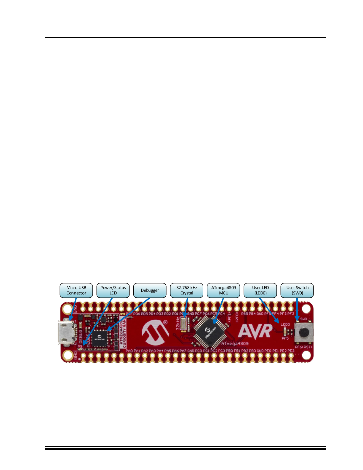
1. Introduction
Micro USB
Connector
Debugger
Power/Status
LED
32.768 kHz
Crystal
User LED
(LED0)
User Switch
(SW0)
ATmega4809
MCU
1.1 Features
• ATmega4809-MFR microcontroller
• One yellow user LED
• One mechanical user switch
• One 32.768 kHz crystal
• Onboard debugger
– Board identification in Atmel Studio/Microchip MPLAB® X
– One green power and status LED
– Programming and debugging
– Virtual COM port (CDC)
– Two logic analyzer channels (DGI GPIO)
• USB powered
• Adjustable target voltage
– MIC5353 LDO regulator controlled by the onboard debugger
– 1.8-5.1V output voltage (limited by USB input voltage)
– 500 mA maximum output current (limited by ambient temperature and output voltage)
ATmega4809 Curiosity Nano
Introduction
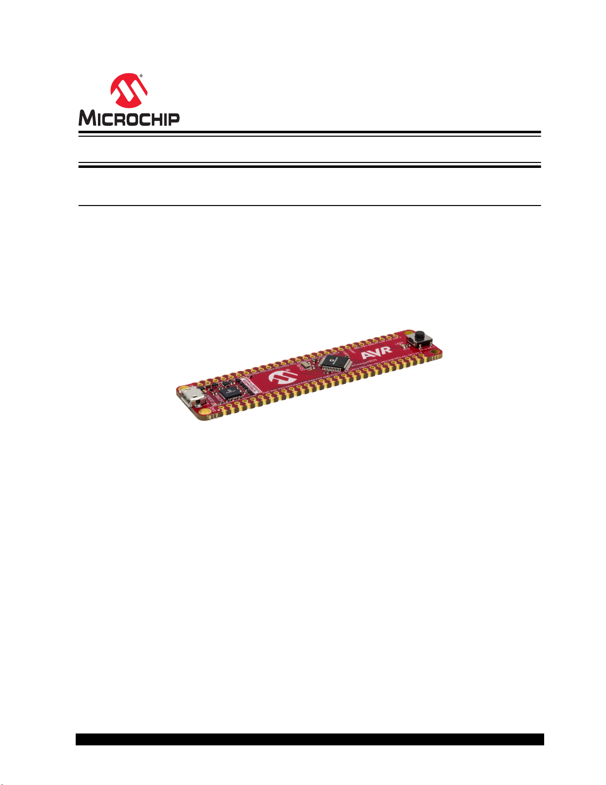
1.2 Kit Overview
The Microchip ATmega4809 Curiosity Nano evaluation kit is a hardware platform to evaluate the
Microchip ATmega4809.
Figure 1-1. ATmega4809 Curiosity Nano Evaluation Kit Overview
© 2018 Microchip Technology Inc.
User Guide
DS50002804A-page 4
Page 5

2. Getting Started
2.1 Curiosity Nano Quick Start
Steps to start exploring the Microchip Curiosity Nano platform:
1. Download Atmel Studio/Microchip MPLAB® X.
2. Launch Atmel Studio/Microchip MPLAB® X.
3. Connect a USB cable (Standard-A to Micro-B or Micro-AB) between the PC and the debug USB
port on the kit.
ATmega4809 Curiosity Nano
Getting Started
When the Curiosity Nano kit is connected to your computer for the first time, the operating system will
perform a driver software installation. The driver file supports both 32- and 64-bit versions of Microsoft
Windows® XP, Windows Vista®, Windows 7, Windows 8, and Windows 10. The drivers for the kit are
included with Atmel Studio/Microchip MPLAB® X.
Once the Curiosity Nano board is powered the green status LED will be lit and Atmel Studio/Microchip
MPLAB® X will auto-detect which Curiosity Nano board is connected. Atmel Studio/Microchip MPLAB® X
will present relevant information like data sheets and kit documentation. The ATmega4809 device is
programmed by the onboard debugger and therefore no external programmer tool is required.
2.2 Design Documentation and Relevant Links
The following list contains links to the most relevant documents and software for the ATmega4809
Curiosity Nano.
• MPLAB® X IDE - MPLAB® X IDE is a software program that runs on a PC (Windows®, Mac OS®,
Linux®) to develop applications for Microchip microcontrollers and digital signal controllers. It is
called an Integrated Development Environment (IDE) because it provides a single integrated
"environment" to develop code for embedded microcontrollers.
• Atmel Studio - Free IDE for the development of C/C++ and assembler code for microcontrollers.
• IAR Embedded Workbench® for AVR® - This is a commercial C/C++ compiler that is available for
8-bit AVR. There is a 30-day evaluation version as well as a 4 KB code-size-limited kick-start
version available from their website.
• Atmel START - Atmel START is an online tool that helps the user to select and configure software
components and tailor your embedded application in a usable and optimized manner.
• Microchip Sample Store - Microchip sample store where you can order samples of devices.
• Data Visualizer - Data Visualizer is a program used for processing and visualizing data. The Data
Visualizer can receive data from various sources such as the EDBG Data Gateway Interface found
on Curiosity Nano and Xplained Pro boards and COM Ports.
• ATmega4809 Curiosity Nano website - Kit information, latest user guide and design
documentation.
• ATmega4809 Curiosity Nano on Microchip Direct - Purchase this kit on Microchip Direct.
®
© 2018 Microchip Technology Inc.
User Guide
DS50002804A-page 5
Page 6

3. Curiosity Nano
Curiosity Nano is an evaluation platform that provides a set of small boards with access to most of the
microcontrollers I/Os. The platform consists of a series of low pin-count microcontroller (MCU) boards,
which are integrated with Atmel Studio/Microchip MPLAB® X to present relevant user guides, application
notes, data sheets, and example code. The platform features a Virtual COM port (CDC) for serial
communication to a host PC and a Data Gateway Interface (DGI) GPIO.
3.1 Onboard Debugger
ATmega4809 Curiosity Nano contains an onboard debugger for programming and debugging. The
onboard debugger is a composite USB device of several interfaces: a debugger, a mass storage device,
a data gateway, and a Virtual COM port (CDC).
Together with Atmel Studio/Microchip MPLAB® X, the onboard debugger interface can program and
debug the ATmega4809.
A Data Gateway Interface (DGI) is available for use with the logic analyzer channels for code
instrumentation, to visualize program flow. DGI GPIOs can be graphed using the Data Visualizer.
ATmega4809 Curiosity Nano
Curiosity Nano
The Virtual COM port is connected to a UART on the ATmega4809 and provides an easy way to
communicate with the target application through terminal software.
The onboard debugger controls one Power and Status LED (marked PS) on the ATmega4809 Curiosity
Nano board. The table below shows how the LED is controlled in different operation modes.
Table 3-1. Onboard Debugger LED Control
Operation Mode Status LED
Boot loader mode LED blink at 1 Hz during power up.
Power-up LED is lit - constant.
Normal operation LED is lit - constant.
Programming Activity indicator; the LED flashes slowly during
Fault The LED flashes fast if a power fault is detected.
Sleep/Off LED is off. The onboard debugger is either in Sleep
3.1.1 Virtual COM Port
A general purpose USB serial bridge between a host PC and a target device.
programming/debugging.
mode or powered down. This can occur if the kit is
externally powered.
3.1.1.1 Overview
The debugger implements a composite USB device that includes a standard Communications Device
Class (CDC) interface, which appears on the host as a Virtual COM Port. The CDC can be used to
stream arbitrary data in both directions between the host and the target: characters sent from the host will
appear in UART form on the CDC TX pin, and UART characters sent into the CDC RX pin will be sent
back to the host.
© 2018 Microchip Technology Inc.
User Guide
DS50002804A-page 6
Page 7

On Windows machines, the CDC will enumerate as Curiosity Virtual COM Port and appear in the Ports
section of the device manager. The COM port number is usually shown here.
Info: On older Windows systems a USB driver is required for CDC. This driver is included in Atmel
Studio and MPLAB X installations.
On Linux machines, the CDC will enumerate and appear as /dev/ttyACM#.
On MAC machines, the CDC will enumerate and appear as /dev/tty.usbmodem#. Depending on which
terminal program is used, it will appear in the available list of modems as usbmodem#.
3.1.1.2 Limitations
Not all UART features are implemented in the debugger CDC. The constraints are outlined here:
• Baud rate must be in the range 1200 bps to 500 kbps. Values outside this range will be capped to
these values, without warning. Baud rate can be changed on-the-fly.
• Character format: only 8-bit characters are supported.
• Parity: can be odd, even, or none.
• Hardware flow control: not supported.
• Stop bits: one or two bits are supported.
3.1.1.3 Signaling
During USB enumeration, the host OS will start both communication and data pipes of the CDC
interface. At this point, it is possible to set and read back baud rate and other UART parameters of the
CDC, but data sending and receiving will not be enabled.
ATmega4809 Curiosity Nano
Curiosity Nano
When a terminal connects on the host, it must assert the DTR signal. This is a virtual control signal that
is implemented on the USB interface but not in hardware on the debugger. Asserting DTR from the host
will indicate to the debugger that a CDC session is active, and it will enable its level shifters (if available),
and start the CDC data send and receive mechanisms.
Deasserting the DTR signal will not disable the level shifters, but it will disable the receiver, so no further
data will be streamed to the host. Data packets that are already queued up for sending to the target will
continue to be sent out, but no further data will be accepted.
3.1.1.4 Advanced Use
CDC Override Mode
In normal operation, the onboard debugger is a true UART bridge between the host and the device.
However, under certain use cases, the debugger can override the Basic Operating mode and use the
CDC pins for other purposes.
Dropping a text file (with extension .txt) into the debugger’s mass storage drive can be used to send
characters out of the CDC TX pin. The text file must start with the characters:
CMD:SEND_UART=
The maximum message length is 50 characters - all remaining data in the frame is ignored.
The default baud rate used in this mode is 9600 bps, but if the CDC is already active or has been
configured, the baud rate last used still applies.
USB-Level Framing Considerations
Sending data from the host to the CDC can be done byte-wise or in blocks, which will be chunked into
64-byte USB frames. Each such frame will be queued up for sending to the CDC TX pin. Sending a small
amount of data per frame can be inefficient, particularly at low baud rates, since the debugger buffers
© 2018 Microchip Technology Inc.
User Guide
DS50002804A-page 7
Page 8

frames, not bytes. A maximum of 4 x 64-byte frames can be active at any time, the debugger will throttle
the incoming frames accordingly. Sending full 64-byte frames containing data is the most efficient.
When receiving data from the target, the debugger will queue up incoming bytes into 64-byte frames,
which are sent to the USB queue for transmission to the host when they are full. Incomplete frames are
also pushed to the USB queue at approximately 100 ms intervals, triggered by USB start-of-frame tokens.
Up to 8 x 64-byte frames can be active at any time. If the host, or software running on it, fails to receive
data fast enough, an overrun will occur. When this happens the last-filled buffer frame will be recycled
instead of being sent to the USB queue, and a full frame of data will be lost. To prevent this occurrence,
the user must ensure that the CDC data pipe is being read continuously, or the incoming data rate must
be reduced.
3.1.2 Mass Storage Disk
A simple way to program the target device through drag and drop with .hex-files.
3.1.2.1 Mass Storage Device
The debugger implements a highly optimized variant of the FAT12 file-system that has a number of
limitations, partly due to the nature of FAT12 itself, and partly due to optimizations made to fulfill its
purpose in this development kit.
ATmega4809 Curiosity Nano
Curiosity Nano
The CURIOSITY drive is USB Chapter 9 compliant as a mass storage device but does not in any way
fulfill the expectations of a general purpose mass storage device. This behavior is intentional.
The debugger enumerates as a Curiosity Nano USB device that can be found in the disk drives section of
the Windows device manager. The CURIOSITY drive appears in the file manager and claims the next
available drive letter in the system.
The CURIOSITY drive contains approximately 1 MB of free space. This does not reflect the size of the
target device's flash in any way. When programming a hex file, the binary data is encoded in ASCII with
metadata providing a large overhead, so 1 MB is a trivially chosen value for disk size.
It is not possible to format the CURIOSITY drive. When programming a file to the target, the filename may
appear in the disk directory listing - this is merely the operating system's view of the directory, which, in
reality, has not been updated. It is not possible to read out the file contents. Removing and replugging the
kit will return the file system to its original state, but the target will still contain the application that has
been previously programmed.
To erase the target device, simply copy a text file starting with "CMD:ERASE" onto the disk.
By default the CURIOSITY drive contains several read-only files for generating icons as well as reporting
status and linking to further information:
• AUTORUN.ICO - Icon file for the Microchip logo.
• AUTORUN.INF - System file required for Windows Explorer to show the icon file.
• KIT-INFO.HTM - Redirect to the development board web site.
• KIT-INFO.TXT - A text file containing details about the kit firmware, name, serial number, and
device.
• STATUS.TXT - A text file containing the programming status of the board.
Info: When STATUS.TXT is updated by the debugger dynamically, the contents may be
cached by the OS and not reflect the correct status.
© 2018 Microchip Technology Inc.
User Guide
DS50002804A-page 8
Page 9
3.1.2.2 Configuration Words/Fuse Bytes
USB
DEBUGGER
PS LED
NC
ID
CDC RX
CDC TX
DBG1
DBG2
VBUS
VOFF
DBG3
DBG0
GND
VTG
CURIOSITY NANO
Fuse Bytes (AVR® Targets)
The debugger does not mask any fuse bits or combinations when writing fuses. It is not possible to
disable UPDI by fuse setting on devices with a dedicated UPDI pin. For devices with a shared/
configurable UPDI pin, be sure not to select an alternate pin function for UPDI either by fuse setting in
Programming mode or by using the I/O view or memory views to modify the memory-mapped fuse
values. Disabling UPDI will render the debugger unable to contact the target device — an external
programmer capable of 12V UPDI activation will be required.
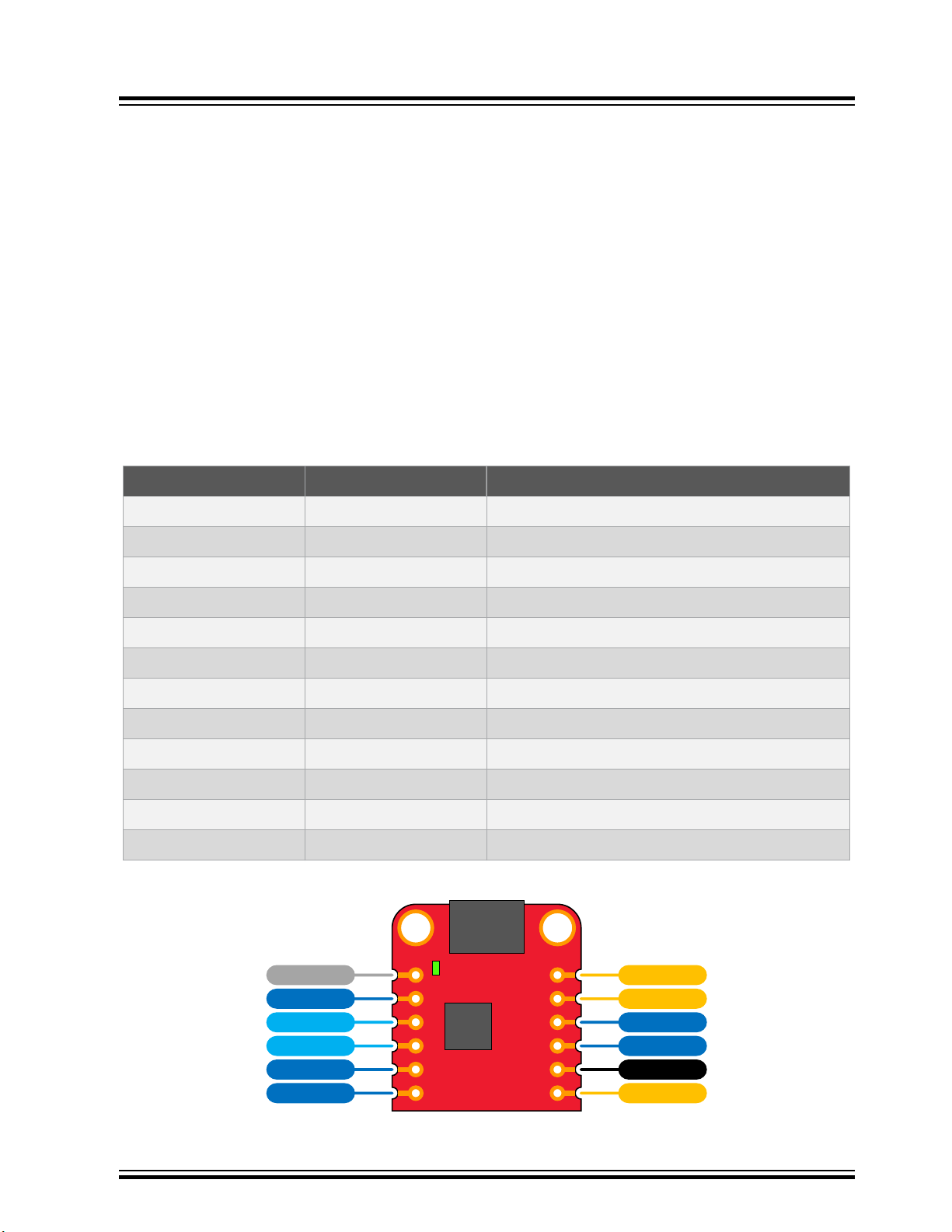
3.2 Curiosity Nano Standard Pinout
The twelve edge connections closest to the USB connector on Curiosity Nano kits have a standardized
pinout. The program/debug pins have different functions depending on the target programming interface
as shown in the table and figure below.
Table 3-2. Curiosity Nano Standard Pinout
Debugger Signal UPDI Target Description
ATmega4809 Curiosity Nano
Curiosity Nano
ID - ID line for extensions.
CDC TX UART RX USB CDC TX line.
CDC RX UART TX USB CDC RX line.
DBG0 UPDI Debug data line.
DBG1 GPIO1 Debug clock line/DGI GPIO
DBG2 GPIO0 DGI GPIO
DBG3 RESET Reset line.
NC - No connect.
VBUS - VBUS voltage for external use.
VOFF - Voltage Off input.
VTG - Target voltage.
GND - Common ground.
Figure 3-1. Curiosity Nano Standard Pinout
© 2018 Microchip Technology Inc.
User Guide
DS50002804A-page 9
Page 10

3.3 Power Supply
The kit is powered through the USB port and contains two regulators for generating 3.3V for the debugger
and an adjustable regulator for the target. The voltage from the USB connector can vary between 4.4V to
5.25V (according to the USB specification) and will limit the maximum voltage to the target. The figure
below shows the entire power supply system on ATmega4809 Curiosity Nano.
Figure 3-2. Power Supply Block Diagram
ATmega4809 Curiosity Nano
Curiosity Nano
3.3.1 Target Regulator
The target voltage regulator is a MIC5353 variable output LDO. The onboard debugger can adjust the
voltage output that is supplied to the kit target section by manipulating the MIC5353's feedback voltage.
The hardware implementation is limited to an approximate voltage range from 1.7V to 5.1V. Additional
output voltage limits are configured in the debugger firmware to ensure that the output voltage never
exceeds the hardware limits of the ATmega4809 microcontroller. The voltage limits configured in the onboard debugger on ATmega4809 Curiosity Nano are 1.8-5.1V.
The target voltage is set to 3.3V in production and can be changed through Atmel Studio. Any change to
the target voltage done in Atmel Studio is persistent, even through a power toggle.
The MIC5353 supports a maximum current load of 500 mA. It is an LDO regulator in a small package,
placed on a small PCB, and the thermal shutdown condition can be reached at lower loads than 500 mA.
The maximum current load depends on the input voltage, set output voltage, and the ambient
temperature. The figure below shows the safe operation area for the regulator, with an input voltage of
5.1V and an ambient temperature of 23°C.
© 2018 Microchip Technology Inc.
User Guide
DS50002804A-page 10
Page 11

Figure 3-3. Target Regulator Safe Operation Area
WARNING
WARNING
3.3.2 External Supply
ATmega4809 Curiosity Nano can be powered by an external voltage instead of the onboard target
regulator. When the Voltage Off (VOFF) pin is shorted to ground (GND) the onboard debugger firmware
disables the target regulator and it is safe to apply an external voltage to the VTG pin.
ATmega4809 Curiosity Nano
Curiosity Nano
Applying an external voltage to the VTG pin without shorting VOFF to GND may cause
permanent damage to the kit.
Absolute maximum external voltage is 5.5V for the level shifters onboard. Applying a higher
voltage may cause permanent damage to the kit.
Programming, debugging, and data streaming is still possible while using external power: the debugger
and signal level shifters will be powered from the USB cable. Both regulators, the debugger, and the level
shifters are powered down when the USB cable is removed.
3.4 Disconnecting the Onboard Debugger
The block diagram below shows all connections between the debugger and the ATmega4809
microcontroller. The rounded boxes represent connections to the board edge on ATmega4809 Curiosity
Nano. The signal names are shown in Figure 3-1 and printed in silkscreen on the bottom side of the
board.
© 2018 Microchip Technology Inc.
User Guide
DS50002804A-page 11
Page 12

DEBUGGER
TARGETLevel-Shift
PA04/PA06
PA07
PA08
PA16
PA00
PA01
USB
DIR x 5
VCC_P3V3
VBUS
VCC_LEVEL VCC_TARGET
DBG0
DBG1
DBG2
DBG3
CDC TX
CDC RX
CDC RX
CDCTX
DBG3
DBG2
DBG1
DBG0
CUT STRAPS
LDO
VOFF
LDO
VBUS VTG
ATmega4809 Curiosity Nano
Figure 3-4. Onboard Debugger Connections to the ATmega4809
Curiosity Nano
By cutting the GPIO straps with a sharp tool, as shown in Figure 3-5, all I/Os connected between the
debugger and the ATmega4809 are completely disconnected. To completely disconnect the target
regulator, cut the VTG strap shown in Figure 3-5.
Info: Cutting the connections to the debugger will disable programming, debugging, data
streaming, and the target power supply. The signals will also be disconnected from the board
edge next to the onboard debugger section.
Info: Solder in 0Ω resistors across the footprints or short-circuit them with tin solder to
reconnect any cut signals.
© 2018 Microchip Technology Inc.
User Guide
DS50002804A-page 12
Page 13

Figure 3-5. Kit Modifications
GPIO straps (bottom side) VTG strap (top side)
3.5 Current Measurement
The power to the ATmega4809 is connected from the onboard power supply to the target voltage supply
(VTG) with a cut strap as shown in Section 3.4 Disconnecting the Onboard Debugger. To measure the
power consumption of the ATmega4809 and other peripherals connected to the board, cut the strap and
connect an ammeter over the strap. The ammeter can be connected between the target VTG pad edge
connector and an external power supply for easy measurement. Alternatively, an external power supply
can be used as described in Section 3.3.2 External Supply.
ATmega4809 Curiosity Nano
Curiosity Nano
Info: The onboard level shifters will draw a small amount of current even when they are not in
use. A maximum of 10 µA can be drawn from the VTG net and an additional 2 µA can be drawn
from each I/O pin connected to a level shifter for a total of 20 µA. Disconnect the onboard
debugger and level shifters as described in Section 3.4 Disconnecting the Onboard Debugger
to prevent any leakage.
© 2018 Microchip Technology Inc.
User Guide
DS50002804A-page 13
Page 14

4. Hardware User Guide
USB
DEBUGGER
ATmega4809
SW0
LED0
PS LED
NC
NC
ID
ID
CDC RX
CDCRX
PB0
CDC TX
CDCTX
PB1
DBG1
DBG1
PF3
DBG2
DBG2
PF2
PA0
PA0
TX
PA1
PA1
RX
PA2
PA2
SDA
PA3
PA3
SCL
PA4
PA4
MOSI
PA5
PA5
MISO
PA6
PA6
SCK
PA7
PA7
SS
GND
GND
PC0
PC0
TX
PC1
PC1
RX
PC2
PC2
PC3
PC3
PB0
PB0
TX
PB1
PB1
RX
PB2
PB2
PB3
PB3
GND
GND
PE0
PE0
PE1
PE1
PE2
PE2
PE3
PE3
VBUS
VBUS
VOFF
VOFF
DBG3
DBG3
PF6 SW0
DBG0
DBG0
UPDI
GND
GND
VTG
VTG
PD7
PD7
AIN7
PD6
PD6
AIN6
PD5
PD5
AIN5
PD4
PD4
AIN4 TCA0 WO4
PD3
PD3
AIN3 TCA0 WO3
PD2
PD2
AIN2
PD1
PD1
AIN1
PD0
PD0
AIN0
GND
GND
PC7
PC7
PC6
PC6
PC5
PC5
PC4
PC4
PF1
PF1
TOSC2
PF0
PF0
TOSC1
PB5
PB5
PB4
PB4
GND
GND
PF5
PF5
LED0
PF4
PF4
PF3
PF3
PF2
PF2
ATmega4809
CURIOSITY NANO
Analog
Debug
I2C
SPI
UART
Shared pin out
Peripheral
Port
PWM
Power
Ground
4.1 Connectors
4.1.1 ATmega4809 Curiosity Nano Pinout
All the ATmega4809 I/O pins are accessible at the edge connectors on the board. The image below
shows the kit pinout.
PF6 and the UPDI pin are only available at the edge connector in the debugger section as long as the
cut-straps on the bottom side are not cut.
PF0 and PF1 are connected to the onboard crystal and not connected to the edge connector by default.
See Section 4.2.3 Crystal for more information.
Figure 4-1. ATmega4809 Curiosity Nano Pinout
ATmega4809 Curiosity Nano
Hardware User Guide
© 2018 Microchip Technology Inc.
User Guide
DS50002804A-page 14
Page 15

4.2 Peripherals
4.2.1 LED
There is one yellow user LED available on the ATmega4809 Curiosity Nano kit that can be controlled by
either GPIO or PWM. The LED can be activated by driving the connected I/O line to GND.
Table 4-1. LED Connection
ATmega4809 Pin Function Shared Functionality
PF5 Yellow LED0 Edge connector
4.2.2 Mechanical Switch
ATmega4809 Curiosity Nano has one mechanical switch. This is a generic user configurable switch.
When the switch is pressed, it will drive the I/O line to ground (GND).
Info: There is a 100 kΩ pull-up resistor connected to the generic user switch. An internal pullup in the ATmega4809 is not required to use the switch.
ATmega4809 Curiosity Nano
Hardware User Guide
Table 4-2. Mechanical Switch
ATmega4809 Pin Description Shared Functionality
PF6 User switch (SW0) DBG3
4.2.3 Crystal
The ATmega4809 Curiosity Nano board has a 32.768 kHz crystal mounted.
The crystal is connected to the ATmega4809 by default, but the GPIOs are routed out to the edge
connector through not mounted resistor footprints. The two I/O lines routed to the edge connector are
disconnected by default to both reduce the chance of contention to the crystal as well as removing
excessive capacitance on the lines when using the crystal. To use the pins PF0 and PF1 as GPIO on the
edge connector, some hardware modification is needed. Solder a 0 Ω resistor or add a solder blob to the
footprints to connect the routing. The crystal should be disconnected when using the pin as GPIO, as this
might harm the crystal.
The 32.768 kHz crystal on ATmega4809 Curiosity Nano is a Kyocera Corporation
ST3215SB32768C0HPWBB 7 pF crystal.
The crystal has been formally tested and matched to the ATmega4809 by Kyocera. The test report is
available in the design documentation distributed with this document for ATmega4809 Curiosity Nano.
Info: Kyocera Crystal Device Corporation crystals that are matched with specific products can
be found on their website: http://prdct-search.kyocera.co.jp/crystal-ic/?p=en_search/
© 2018 Microchip Technology Inc.
User Guide
DS50002804A-page 15
Page 16

Table 4-3. Crystal Connections
ATmega4809 Pin Function Shared Functionality
PF0 TOSC1 (Crystal input) Edge connector
PF1 TOSC2 (Crystal output) Edge connector
Figure 4-2. GPIO Connection Footprint
4.3 Onboard Debugger Implementation
ATmega4809 Curiosity Nano features an onboard debugger that can be used to program and debug the
ATmega4809 using UPDI. The onboard debugger also includes a Virtual Com port interface over UART
and DGI GPIO. Atmel Studio/Microchip MPLAB® X can be used as a front-end for the onboard debugger
for programming and debugging. Data Visualizer can be used as a front-end for the CDC and DGI GPIO.
ATmega4809 Curiosity Nano
Hardware User Guide
4.3.1 Onboard Debugger Connections
The table below shows the connections between the target and the debugger section. All connections
between the target and the debugger are tri-stated as long as the debugger is not actively using the
interface, hence there is little contamination of the signals, the pins can be configured to anything the
user wants.
For further information on how to use the capabilities of the onboard debugger, see Section 3. Curiosity
Nano.
Table 4-4. Onboard Debugger Connections
ATmega4809
Pin
PB1 CDC TX UART RX (ATmega4809 RX line) Edge connector
PB0 CDC RX UART TX (ATmega4809 TX line) Edge connector
UPDI DBG0 UPDI
PF3 DBG1 GPIO Edge connector
PF2 DBG2 GPIO Edge connector
PF6 DBG3 RESET/GPIO User switch
VCC_TARGET VCC_LEVEL 1.8-5.1V Supply
Debugger Pin Function Shared Functionality
GND GND Common ground
© 2018 Microchip Technology Inc.
User Guide
DS50002804A-page 16
Page 17

5. Hardware Revision History
This user guide provides the latest available revision of the kit. This chapter contains information about
known issues, a revision history of older revisions, and how older revisions differ from the latest revision.
5.1 Identifying Product ID and Revision
The revision and product identifier of Curiosity Nano boards can be found in two ways; either through
Atmel Studio/Microchip MPLAB® X or by looking at the sticker on the bottom side of the PCB.
By connecting a Curiosity Nano board to a computer with Atmel Studio/Microchip MPLAB® X running, an
information window will pop up. The first six digits of the serial number, which is listed under kit details,
contain the product identifier and revision.
The same information can be found on the sticker on the bottom side of the PCB. Most kits will print the
identifier and revision in plain text as A09-nnnn\rr, where nnnn is the identifier and rr is the revision.
Boards with limited space have a sticker with only a QR-code, which contains a serial number string.
The serial number string has the following format:
ATmega4809 Curiosity Nano
Hardware Revision History
"nnnnrrssssssssss"
n = product identifier
r = revision
s = serial number
The product identifier for ATmega4809 Curiosity Nano is A09-3094.
5.2 Revision 5
Revision 5 is the initially released revision.
© 2018 Microchip Technology Inc.
User Guide
DS50002804A-page 17
Page 18

6. Document Revision History
Doc. rev. Date Comment
A 10/2018 Initial document release.
ATmega4809 Curiosity Nano
Document Revision History
© 2018 Microchip Technology Inc.
User Guide
DS50002804A-page 18
Page 19

7. Appendix
GND
10
VDDANA
9
PA08
11
PA09
12
PA10
13
PA11
14
PA14
15
PA15
16
PA27
25
RESETN
26
PA28
27
GND
28
VDDCORE
29
VDDIN
30
SWDCLK/PA30
31
SWDIO/PA31
32
GND
3
EP
7
G
N
GGD
3
E
P
7
DBG0_CTRL
7
47k
R101
27k
R104
7
4
7
k
R
10127
k
R
104
DBG1_CTRL
REG_ENABLE
47k
4
7
k
R103
47k
47k
R102
47k
47k
R105
47k
4
7
k
R100
SRST
DBG2_CTRL
47k
4
7
k
R109
REG_ADJUST
DBG2_GPIO
VBUS_ADC
2 3
1k
R112
1
k
R
112
VTG_EN
VBUS_ADC
47k
4
7
k
R111
7.1 Schematic
Figure 7-1. ATmega4809 Curiosity Nano Schematic
ATmega4809 Curiosity Nano
Appendix
© 2018 Microchip Technology Inc.
User Guide
DS50002804A-page 19
Page 20

PC3
13
VDD
14
GND
15
PC4
16
PC5
17
PC6
18
PC7
19
PD0
20
PD1
21
PD2
22
PD3
23
PD4
24
PF3
37
PF4
38
PF5
39
PF6
40
UPDI
41
VDD
42
GND
43
(EXTCLK)PA0
44
PA1
45
PA2
46
PA3
47
PA4
48
PC3
PC4
PC5
PC6
PC7
PD0
PD1
PD2
PD3
PD4
PA3_I2C_SCL
PA1_UART0_RX
UPDI
PF5
PF3
PF1_TOSC2
PF0_TOSC1
PA2_I2C_SDA
PA0_UART0_TX
PF4
PA4_SPI_MOSI
1k
R203
1
k
R
203
PF6
PF6
PF5
1k
1
k
R202
YELLOW LED
SML-D12Y1WT86
21
D200
TS604VM1-035CR
1 3
42
CDC_TX
CDC_RX
DBG2
DBG1
DBG3
DBG0
ID_SYS
VOFF
100k
R200
100
k
R20
0
ATmega4809 Curiosity Nano
Appendix
© 2018 Microchip Technology Inc.
User Guide
DS50002804A-page 20
Page 21

7.2 Connecting External Debuggers
USB
DEBUGGER
PS LED
NC
ID
CDC RX
CDC TX
DBG1
DBG2
VBUS
VOFF
DBG3
DBG0
GND
VTG
CURIOSITY NANO
2
3
4
5
678
1
VDD
Ground
DATA
2 = VDD
3 = Ground
4 = PGD
5 = Unused
6 = Unused
7 = Unused
8 = Unused
1 = Unused
MPLAB® PICkit™ 4
Even though there is an onboard debugger, external debuggers can be connected directly to
ATmega4809 Curiosity Nano to program/debug the ATmega4809. The onboard debugger keeps all the
pins connected to the ATmega4809 and board edge in tri-state when not actively used. Therefore, the
onboard debugger will not interfere with any external debug tools.
Figure 7-2. Connecting the PICkit™ 4 to ATmega4809 Curiosity Nano
ATmega4809 Curiosity Nano
Appendix
© 2018 Microchip Technology Inc.
User Guide
DS50002804A-page 21
Page 22

USB
DEBUGGER
PS LED
NC
ID
CDC RX
CDC TX
DBG1
DBG2
VBUS
VOFF
DBG3
DBG0
GND
VTG
CURIOSITY NANO
V
DD
Ground
DATA
AVR®
SAM
3 = UPDI
4 = VTG
5 = Unused
6 = Unused
7 = Unused
8 = Unused
1 = Unused
2 = GND
9 = Unused
10 = Unused
Atmel-ICE
2
1
9
10
CAUTION
ATmega4809 Curiosity Nano
Figure 7-3. Connecting the Atmel-ICE to ATmega4809 Curiosity Nano
Appendix
To avoid contention between the external debugger and the onboard debugger, do not start any
programming/debug operation with the onboard debugger through Atmel Studio/Microchip
MPLAB® X or mass storage programming while the external tool is active.
7.3 Getting Started with IAR
IAR Embedded Workbench® for AVR® is a proprietary high-efficiency compiler which is not based on
GCC. Programming and debugging of ATmega4809 Curiosity Nano is supported in IAR™ Embedded
Workbench for AVR using the Atmel-ICE interface. Some initial settings must be set up in the project to
get the programming and debugging to work.
The following steps will explain how to get your project ready for programming and debugging:
1. Make sure you have opened the project you want to configure. Open the OPTIONS dialog for the
project.
2. In the category General Options, select the Target tab. Select the device for the project, or, if not
listed, the core of the device.
3. In the category Debugger, select the Setup tab. Select Atmel-ICE as the driver.
© 2018 Microchip Technology Inc.
User Guide
DS50002804A-page 22
Page 23

ATmega4809 Curiosity Nano
Appendix
4. In the category Debugger > Atmel-ICE, select the Atmel-ICE 1 tab. Select UPDI as the interface
and, optionally, select the UPDI frequency.
Info: If the selection of Debug Port, mentioned in step 4, is grayed out, the interface is
preselected, and the user can skip this configuration step.
Figure 7-4. Select Target Device
© 2018 Microchip Technology Inc.
User Guide
DS50002804A-page 23
Page 24

Figure 7-5. Select Debugger
ATmega4809 Curiosity Nano
Appendix
Figure 7-6. Configure Interface
© 2018 Microchip Technology Inc.
User Guide
DS50002804A-page 24
Page 25

ATmega4809 Curiosity Nano
The Microchip Web Site
Microchip provides online support via our web site at http://www.microchip.com/. This web site is used as
a means to make files and information easily available to customers. Accessible by using your favorite
Internet browser, the web site contains the following information:
• Product Support – Data sheets and errata, application notes and sample programs, design
resources, user’s guides and hardware support documents, latest software releases and archived
software
• General Technical Support – Frequently Asked Questions (FAQ), technical support requests,
online discussion groups, Microchip consultant program member listing
• Business of Microchip – Product selector and ordering guides, latest Microchip press releases,
listing of seminars and events, listings of Microchip sales offices, distributors and factory
representatives
Customer Change Notification Service
Microchip’s customer notification service helps keep customers current on Microchip products.
Subscribers will receive e-mail notification whenever there are changes, updates, revisions or errata
related to a specified product family or development tool of interest.
To register, access the Microchip web site at http://www.microchip.com/. Under “Support”, click on
“Customer Change Notification” and follow the registration instructions.
Customer Support
Users of Microchip products can receive assistance through several channels:
• Distributor or Representative
• Local Sales Office
• Field Application Engineer (FAE)
• Technical Support
Customers should contact their distributor, representative or Field Application Engineer (FAE) for support.
Local sales offices are also available to help customers. A listing of sales offices and locations is included
in the back of this document.
Technical support is available through the web site at: http://www.microchip.com/support
Microchip Devices Code Protection Feature
Note the following details of the code protection feature on Microchip devices:
• Microchip products meet the specification contained in their particular Microchip Data Sheet.
• Microchip believes that its family of products is one of the most secure families of its kind on the
market today, when used in the intended manner and under normal conditions.
• There are dishonest and possibly illegal methods used to breach the code protection feature. All of
these methods, to our knowledge, require using the Microchip products in a manner outside the
operating specifications contained in Microchip’s Data Sheets. Most likely, the person doing so is
engaged in theft of intellectual property.
• Microchip is willing to work with the customer who is concerned about the integrity of their code.
© 2018 Microchip Technology Inc.
User Guide
DS50002804A-page 25
Page 26

ATmega4809 Curiosity Nano
• Neither Microchip nor any other semiconductor manufacturer can guarantee the security of their
code. Code protection does not mean that we are guaranteeing the product as “unbreakable.”
Code protection is constantly evolving. We at Microchip are committed to continuously improving the
code protection features of our products. Attempts to break Microchip’s code protection feature may be a
violation of the Digital Millennium Copyright Act. If such acts allow unauthorized access to your software
or other copyrighted work, you may have a right to sue for relief under that Act.
Legal Notice
Information contained in this publication regarding device applications and the like is provided only for
your convenience and may be superseded by updates. It is your responsibility to ensure that your
application meets with your specifications. MICROCHIP MAKES NO REPRESENTATIONS OR
WARRANTIES OF ANY KIND WHETHER EXPRESS OR IMPLIED, WRITTEN OR ORAL, STATUTORY
OR OTHERWISE, RELATED TO THE INFORMATION, INCLUDING BUT NOT LIMITED TO ITS
CONDITION, QUALITY, PERFORMANCE, MERCHANTABILITY OR FITNESS FOR PURPOSE.
Microchip disclaims all liability arising from this information and its use. Use of Microchip devices in life
support and/or safety applications is entirely at the buyer’s risk, and the buyer agrees to defend,
indemnify and hold harmless Microchip from any and all damages, claims, suits, or expenses resulting
from such use. No licenses are conveyed, implicitly or otherwise, under any Microchip intellectual
property rights unless otherwise stated.
Trademarks
The Microchip name and logo, the Microchip logo, AnyRate, AVR, AVR logo, AVR Freaks, BitCloud,
chipKIT, chipKIT logo, CryptoMemory, CryptoRF, dsPIC, FlashFlex, flexPWR, Heldo, JukeBlox, KeeLoq,
Kleer, LANCheck, LINK MD, maXStylus, maXTouch, MediaLB, megaAVR, MOST, MOST logo, MPLAB,
OptoLyzer, PIC, picoPower, PICSTART, PIC32 logo, Prochip Designer, QTouch, SAM-BA, SpyNIC, SST,
SST Logo, SuperFlash, tinyAVR, UNI/O, and XMEGA are registered trademarks of Microchip Technology
Incorporated in the U.S.A. and other countries.
ClockWorks, The Embedded Control Solutions Company, EtherSynch, Hyper Speed Control, HyperLight
Load, IntelliMOS, mTouch, Precision Edge, and Quiet-Wire are registered trademarks of Microchip
Technology Incorporated in the U.S.A.
Adjacent Key Suppression, AKS, Analog-for-the-Digital Age, Any Capacitor, AnyIn, AnyOut, BodyCom,
CodeGuard, CryptoAuthentication, CryptoAutomotive, CryptoCompanion, CryptoController, dsPICDEM,
dsPICDEM.net, Dynamic Average Matching, DAM, ECAN, EtherGREEN, In-Circuit Serial Programming,
ICSP, INICnet, Inter-Chip Connectivity, JitterBlocker, KleerNet, KleerNet logo, memBrain, Mindi, MiWi,
motorBench, MPASM, MPF, MPLAB Certified logo, MPLIB, MPLINK, MultiTRAK, NetDetach, Omniscient
Code Generation, PICDEM, PICDEM.net, PICkit, PICtail, PowerSmart, PureSilicon, QMatrix, REAL ICE,
Ripple Blocker, SAM-ICE, Serial Quad I/O, SMART-I.S., SQI, SuperSwitcher, SuperSwitcher II, Total
Endurance, TSHARC, USBCheck, VariSense, ViewSpan, WiperLock, Wireless DNA, and ZENA are
trademarks of Microchip Technology Incorporated in the U.S.A. and other countries.
SQTP is a service mark of Microchip Technology Incorporated in the U.S.A.
Silicon Storage Technology is a registered trademark of Microchip Technology Inc. in other countries.
GestIC is a registered trademark of Microchip Technology Germany II GmbH & Co. KG, a subsidiary of
Microchip Technology Inc., in other countries.
All other trademarks mentioned herein are property of their respective companies.
© 2018 Microchip Technology Inc.
User Guide
DS50002804A-page 26
Page 27

ATmega4809 Curiosity Nano
©
2018, Microchip Technology Incorporated, Printed in the U.S.A., All Rights Reserved.
ISBN: 978-1-5224-3628-7
Quality Management System Certified by DNV
ISO/TS 16949
Microchip received ISO/TS-16949:2009 certification for its worldwide headquarters, design and wafer
fabrication facilities in Chandler and Tempe, Arizona; Gresham, Oregon and design centers in California
and India. The Company’s quality system processes and procedures are for its PIC® MCUs and dsPIC
DSCs, KEELOQ® code hopping devices, Serial EEPROMs, microperipherals, nonvolatile memory and
analog products. In addition, Microchip’s quality system for the design and manufacture of development
systems is ISO 9001:2000 certified.
®
© 2018 Microchip Technology Inc.
User Guide
DS50002804A-page 27
Page 28

Worldwide Sales and Service
AMERICAS ASIA/PACIFIC ASIA/PACIFIC EUROPE
Corporate Office
2355 West Chandler Blvd.
Chandler, AZ 85224-6199
Tel: 480-792-7200
Fax: 480-792-7277
Technical Support:
http://www.microchip.com/
support
Web Address:
www.microchip.com
Atlanta
Duluth, GA
Tel: 678-957-9614
Fax: 678-957-1455
Austin, TX
Tel: 512-257-3370
Boston
Westborough, MA
Tel: 774-760-0087
Fax: 774-760-0088
Chicago
Itasca, IL
Tel: 630-285-0071
Fax: 630-285-0075
Dallas
Addison, TX
Tel: 972-818-7423
Fax: 972-818-2924
Detroit
Novi, MI
Tel: 248-848-4000
Houston, TX
Tel: 281-894-5983
Indianapolis
Noblesville, IN
Tel: 317-773-8323
Fax: 317-773-5453
Tel: 317-536-2380
Los Angeles
Mission Viejo, CA
Tel: 949-462-9523
Fax: 949-462-9608
Tel: 951-273-7800
Raleigh, NC
Tel: 919-844-7510
New York, NY
Tel: 631-435-6000
San Jose, CA
Tel: 408-735-9110
Tel: 408-436-4270
Canada - Toronto
Tel: 905-695-1980
Fax: 905-695-2078
Australia - Sydney
Tel: 61-2-9868-6733
China - Beijing
Tel: 86-10-8569-7000
China - Chengdu
Tel: 86-28-8665-5511
China - Chongqing
Tel: 86-23-8980-9588
China - Dongguan
Tel: 86-769-8702-9880
China - Guangzhou
Tel: 86-20-8755-8029
China - Hangzhou
Tel: 86-571-8792-8115
China - Hong Kong SAR
Tel: 852-2943-5100
China - Nanjing
Tel: 86-25-8473-2460
China - Qingdao
Tel: 86-532-8502-7355
China - Shanghai
Tel: 86-21-3326-8000
China - Shenyang
Tel: 86-24-2334-2829
China - Shenzhen
Tel: 86-755-8864-2200
China - Suzhou
Tel: 86-186-6233-1526
China - Wuhan
Tel: 86-27-5980-5300
China - Xian
Tel: 86-29-8833-7252
China - Xiamen
Tel: 86-592-2388138
China - Zhuhai
Tel: 86-756-3210040
India - Bangalore
Tel: 91-80-3090-4444
India - New Delhi
Tel: 91-11-4160-8631
India - Pune
Tel: 91-20-4121-0141
Japan - Osaka
Tel: 81-6-6152-7160
Japan - Tokyo
Tel: 81-3-6880- 3770
Korea - Daegu
Tel: 82-53-744-4301
Korea - Seoul
Tel: 82-2-554-7200
Malaysia - Kuala Lumpur
Tel: 60-3-7651-7906
Malaysia - Penang
Tel: 60-4-227-8870
Philippines - Manila
Tel: 63-2-634-9065
Singapore
Tel: 65-6334-8870
Taiwan - Hsin Chu
Tel: 886-3-577-8366
Taiwan - Kaohsiung
Tel: 886-7-213-7830
Taiwan - Taipei
Tel: 886-2-2508-8600
Thailand - Bangkok
Tel: 66-2-694-1351
Vietnam - Ho Chi Minh
Tel: 84-28-5448-2100
Austria - Wels
Tel: 43-7242-2244-39
Fax: 43-7242-2244-393
Denmark - Copenhagen
Tel: 45-4450-2828
Fax: 45-4485-2829
Finland - Espoo
Tel: 358-9-4520-820
France - Paris
Tel: 33-1-69-53-63-20
Fax: 33-1-69-30-90-79
Germany - Garching
Tel: 49-8931-9700
Germany - Haan
Tel: 49-2129-3766400
Germany - Heilbronn
Tel: 49-7131-67-3636
Germany - Karlsruhe
Tel: 49-721-625370
Germany - Munich
Tel: 49-89-627-144-0
Fax: 49-89-627-144-44
Germany - Rosenheim
Tel: 49-8031-354-560
Israel - Ra’anana
Tel: 972-9-744-7705
Italy - Milan
Tel: 39-0331-742611
Fax: 39-0331-466781
Italy - Padova
Tel: 39-049-7625286
Netherlands - Drunen
Tel: 31-416-690399
Fax: 31-416-690340
Norway - Trondheim
Tel: 47-72884388
Poland - Warsaw
Tel: 48-22-3325737
Romania - Bucharest
Tel: 40-21-407-87-50
Spain - Madrid
Tel: 34-91-708-08-90
Fax: 34-91-708-08-91
Sweden - Gothenberg
Tel: 46-31-704-60-40
Sweden - Stockholm
Tel: 46-8-5090-4654
UK - Wokingham
Tel: 44-118-921-5800
Fax: 44-118-921-5820
© 2018 Microchip Technology Inc.
User Guide
DS50002804A-page 28
 Loading...