

Page 1
January - June 2007
2007 Product Selector Guide
Page 2

Product Profile
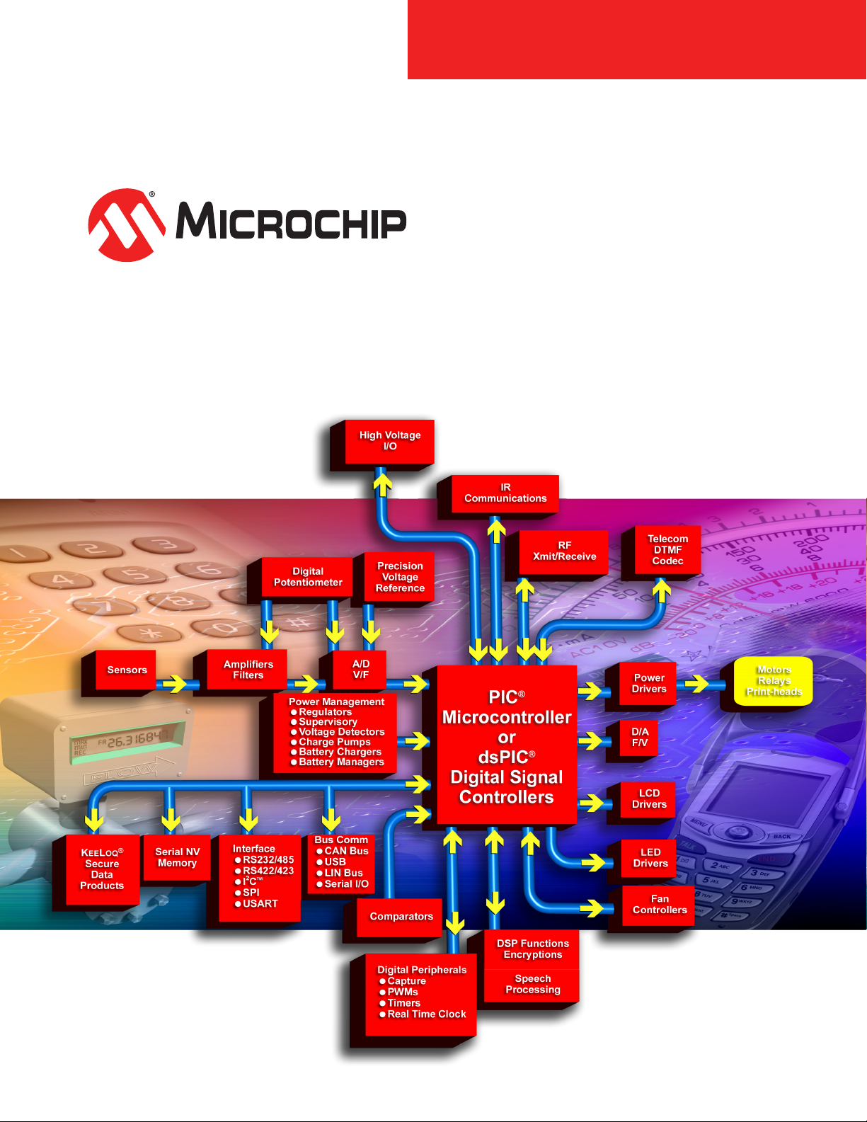
8-bit PIC® Microcontrollers
Microchip’s 8-bit PIC® microcontrollers combine high-performance, low cost and small package size to offer the best price/
performance ratio in the industry. Based on a powerful RISC core, these 8-bit PIC® microcontrollers fall into three product architecture
categories, providing a variety of options for any application requirement:
• Baseline 8-bit architecture: 12-bit instruction set, 6-44 pin count, 384-3.5 Kbytes program memory, up to 5 MIPS
• Mid-Range 8-bit architecture: 14-bit instruction set, 8-68 pin count, 896-14 Kbytes program memory, up to 5 MIPS
• High-Performance (PIC18) 8-bit architecture: 16-bit instruction set, 18-100 pin count, 8-128 Kbytes program memory, up to 16 MIPS
The common architecture provides users with an easy migration path from 6 to 100 pins among all families, with little or no code
change required. Advanced features available are:
• Sophisticated timing peripherals
• Embedded analog peripherals, including A/D and D/A converters, comparators, PBOR, PLVD, DAC, Vref, Op Amps and PSMC
• Communications peripherals (I2C™/SPI/USB/CAN, LIN, USARTs and Ethernet)
• Low-power, single-chip RF and Ethernet solutions targeting connectivity for high-volume embedded control applications
• Battery management solutions
• Flexible programming options including In-Circuit Serial Programming™ technology, self-programming (Enhanced Flash),
One-Time-Programmable (OTP), QTP, SQTP and ROM
16-bit PIC® Microcontrollers
The PIC24 microcontrollers build upon the high performance, wide selection of peripherals, Flash memory sizes and packaging
choices found in the 8-bit PIC18 family. The PIC24 architecture, paired with the optimized MPLAB® C30 C Compiler, provides the high
throughput and C code density needed to achieve system performance goals and product launch schedules.
• Leadership 16-bit microcontroller performance and C code efficiency
• Extension of the 8-bit PIC18 microcontroller performance, memory and peripherals
• Easy migration path to dsPIC® digital signal controllers with over 40 MIPS, DSP capability and MPLAB® IDE compatibility
16-bit dsPIC® Digital Signal Controllers (DSCs)
Microchip’s 16-bit high-performance digital signal controllers combine, in a single core, the best features of microcontrollers with the
best features of DSPs. These dsPIC DSCs reach speeds of up to 40 MIPS, are very efficient for C programming, and have Flash, data
EEPROM, powerful peripherals and a variety of software libraries that allow high-performance embedded solutions to be designed
effortlessly and rapidly. With a familiar microcontroller “feel”, tools and design environment, these dsPIC DSCs target applications,
such as motor control and power conversion, speech and audio, internet and modem connectivity, telecom, encryption, high-speed
sensing and automotive applications.
Stand-Alone Analog & Interface Products
Microchip offers a broad portfolio of analog and related products:
• Linear and Mixed-Signal. ADCs/DACs, digital potentiometers, op amps and comparators.
• Power and Battery Management. LDO and switching regulators, charge pumps, voltage references, CPU/system
supervisors and voltage detectors, battery chargers and power MOSFET drivers.
• Thermal Management. Temperature sensors (logic output, voltage output, and serial output), brushless DC fan controllers and
fan fault detectors.
• Interface. Peripheral products supporting industry-standard networking protocols like CAN, LIN and infrared (including IrDA® Standard
infrared), as well as products that provide embedded system input/output expansion capability.
Secure Data Products
Microchip’s KeeLoq® code-hopping algorithm combines high security, a small package outline and a very low cost to make this an ideal
cryptographic solution for RKE and PKE authentication applications. The KeeLoq code-hopping technology creates a high degree of
security using a long code word length together with encryption and synchronization techniques.
Memory Products
Microchip offers one of the broadest selections of serial EEPROMs in densities from 128 bits to 1 Mbit, with operating voltages down
to 1.8V, in all popular bus protocols (I2C™, Microwire and SPI compatible). They are available in all standard temperature ranges from
-40°C to +125°C, up to 16 Kbits in 5-lead SOT-23 and up to 256 Kbits in 8-lead MSOP.
Development Systems
Microchip offers a full range of microcontroller, memory and analog development systems, including the MPLAB® REAL ICE™
in-circuit emulator; free MPLAB Integrated Development Environment; MPLAB C18 and C30 Compilers; the MPLAB ICD 2 In-Circuit
Debugger, MPLAB PM3 full-featured device programmer; PICSTART® low-cost development system; the PICkit™ 2 Flash Starter Kit,
SEEVAL® Serial EEPROM Evaluation Kit and various demonstration boards. Microchip has shipped nearly half a million development
systems worldwide.
Page 3

TABLE OF CONTENTS
CURRENT 16-BIT CONTROLLER FAMILY PRODUCTS . . . . . . . . . . . . . . . . . . . . . . . 6
dsPIC® Digital Signal Controller (DSC) Family . . . . . . . . . . . . . . . . . . . . . . . . . . . . . . . . . . . . . . . . . . .6
dsPIC30F General Purpose Family: 30 MIPS. . . . . . . . . . . . . . . . . . . . . . . . . . . . . . . . . . . . . . . . .6
dsPIC30F Motor Control and Power Conversion Family: 30 MIPS. . . . . . . . . . . . . . . . . . . . . . . . .6
dsPIC30F SMPS and Digital Power Conversion: 30 MIPS . . . . . . . . . . . . . . . . . . . . . . . . . . . . . . .7
dsPIC30F Sensor Family: 30 MIPS. . . . . . . . . . . . . . . . . . . . . . . . . . . . . . . . . . . . . . . . . . . . . . . . .7
dsPIC33F General Purpose Family: 40 MIPS. . . . . . . . . . . . . . . . . . . . . . . . . . . . . . . . . . . . . . . . .8
dsPIC33F Motor Control Family: 40 MIPS . . . . . . . . . . . . . . . . . . . . . . . . . . . . . . . . . . . . . . . . . . .9
PIC24 16-Bit Microcontroller (MCU) Family. . . . . . . . . . . . . . . . . . . . . . . . . . . . . . . . . . . . . . . . . . . . .10
PIC24FJ Family: 16 MIPS. . . . . . . . . . . . . . . . . . . . . . . . . . . . . . . . . . . . . . . . . . . . . . . . . . . . . . .10
PIC24FJ Family: 16 MIPS. . . . . . . . . . . . . . . . . . . . . . . . . . . . . . . . . . . . . . . . . . . . . . . . . . . . . . .11
PIC24HJ Family: 40 MIPS. . . . . . . . . . . . . . . . . . . . . . . . . . . . . . . . . . . . . . . . . . . . . . . . . . . . . . .11
FUTURE 16-BIT CONTROLLER FAMILY PRODUCTS . . . . . . . . . . . . . . . . . . . . . . . 13
dsPIC® Digital Signal Controller (DSC) Family . . . . . . . . . . . . . . . . . . . . . . . . . . . . . . . . . . . . . . . . . .13
dsPIC33F General Purpose Family: 40 MIPS. . . . . . . . . . . . . . . . . . . . . . . . . . . . . . . . . . . . . . . .13
dsPIC33F Motor Control Family: 40 MIPS . . . . . . . . . . . . . . . . . . . . . . . . . . . . . . . . . . . . . . . . . .14
PIC24 16-Bit Microcontroller (MCU) Family. . . . . . . . . . . . . . . . . . . . . . . . . . . . . . . . . . . . . . . . . . . . .15
PIC24FJ Family: 16 MIPS. . . . . . . . . . . . . . . . . . . . . . . . . . . . . . . . . . . . . . . . . . . . . . . . . . . . . . .15
PIC24HJ Family: 40 MIPS. . . . . . . . . . . . . . . . . . . . . . . . . . . . . . . . . . . . . . . . . . . . . . . . . . . . . . .15
CURRENT ANALOG/INTERFACE PRODUCTS. . . . . . . . . . . . . . . . . . . . . . . . . . . . . 16
THERMAL MANAGEMENT PRODUCTS – Temperature Sensors. . . . . . . . . . . . . . . . . . . . . . . . . . .16
Logic Output Temperature Sensors . . . . . . . . . . . . . . . . . . . . . . . . . . . . . . . . . . . . . . . . . . . . . . .16
Voltage Output Temperature Sensors. . . . . . . . . . . . . . . . . . . . . . . . . . . . . . . . . . . . . . . . . . . . . .16
Serial Output Temperature Sensors . . . . . . . . . . . . . . . . . . . . . . . . . . . . . . . . . . . . . . . . . . . . . . .16
THERMAL MANAGEMENT PRODUCTS – Brushless DC Fan Controllers and
Fan Fault Detectors. . . . . . . . . . . . . . . . . . . . . . . . . . . . . . . . . . . . . . . . . . . . . . . . . . . . . . . . . . . .17
POWER MANAGEMENT – Voltage References. . . . . . . . . . . . . . . . . . . . . . . . . . . . . . . . . . . . . . . . .18
POWER MANAGEMENT – Linear Regulators . . . . . . . . . . . . . . . . . . . . . . . . . . . . . . . . . . . . . . . . . .19
50 mA to 250 mA Low-Dropout Linear Regulators . . . . . . . . . . . . . . . . . . . . . . . . . . . . . . . . . . . .19
300 mA Low Dropout Linear Regulators . . . . . . . . . . . . . . . . . . . . . . . . . . . . . . . . . . . . . . . . . . . .20
500 mA to 800 mA Low Dropout Linear Regulators . . . . . . . . . . . . . . . . . . . . . . . . . . . . . . . . . . .20
1A and Above Low Dropout Linear Regulators . . . . . . . . . . . . . . . . . . . . . . . . . . . . . . . . . . . . . . .20
Application Specific Low Dropout Linear Regulators. . . . . . . . . . . . . . . . . . . . . . . . . . . . . . . . . . .20
Power Management Combination Products . . . . . . . . . . . . . . . . . . . . . . . . . . . . . . . . . . . . . . . . .20
POWER MANAGEMENT – Switching Regulators. . . . . . . . . . . . . . . . . . . . . . . . . . . . . . . . . . . . . . . .21
POWER MANAGEMENT – PWM Controllers . . . . . . . . . . . . . . . . . . . . . . . . . . . . . . . . . . . . . . . . . . .22
POWER MANAGEMENT – Charge Pump DC-to-DC Converters . . . . . . . . . . . . . . . . . . . . . . . . . . . .22
Inverting or Doubling Charge Pumps . . . . . . . . . . . . . . . . . . . . . . . . . . . . . . . . . . . . . . . . . . . . . .22
PAGE i
Page 4

POWER MANAGEMENT – CPU/System Supervisors . . . . . . . . . . . . . . . . . . . . . . . . . . . . . . . . . . . .23
Multi-Function Charge Pumps. . . . . . . . . . . . . . . . . . . . . . . . . . . . . . . . . . . . . . . . . . . . . . . . . . . .23
Inverting and Doubling Charge Pumps . . . . . . . . . . . . . . . . . . . . . . . . . . . . . . . . . . . . . . . . . . . . .23
Regulated Charge Pumps. . . . . . . . . . . . . . . . . . . . . . . . . . . . . . . . . . . . . . . . . . . . . . . . . . . . . . .23
POWER MANAGEMENT – Voltage Detectors . . . . . . . . . . . . . . . . . . . . . . . . . . . . . . . . . . . . . . . . . .24
POWER MANAGEMENT – Power MOSFET Drivers . . . . . . . . . . . . . . . . . . . . . . . . . . . . . . . . . . . . .25
Low-Side Drivers, 0.5A to 1.2A Peak Output Current . . . . . . . . . . . . . . . . . . . . . . . . . . . . . . . . . .25
Low-Side Drivers, 1.5A Peak Output Current . . . . . . . . . . . . . . . . . . . . . . . . . . . . . . . . . . . . . . . .25
Low-Side Drivers, 2.0A to 12.0A Peak Output Current . . . . . . . . . . . . . . . . . . . . . . . . . . . . . . . . .26
High-Side/Low-Side Drivers . . . . . . . . . . . . . . . . . . . . . . . . . . . . . . . . . . . . . . . . . . . . . . . . . . . . .26
POWER MANAGEMENT – Battery Chargers . . . . . . . . . . . . . . . . . . . . . . . . . . . . . . . . . . . . . . . . . . .27
POWER MANAGEMENT – Hot Swap Controllers. . . . . . . . . . . . . . . . . . . . . . . . . . . . . . . . . . . . . . . .28
LINEAR – Op Amps. . . . . . . . . . . . . . . . . . . . . . . . . . . . . . . . . . . . . . . . . . . . . . . . . . . . . . . . . . . . . . .28
LINEAR – High Precision Operational Amplifiers. . . . . . . . . . . . . . . . . . . . . . . . . . . . . . . . . . . . . . . . .30
Chopper Stabilized . . . . . . . . . . . . . . . . . . . . . . . . . . . . . . . . . . . . . . . . . . . . . . . . . . . . . . . . . . . .30
Auto-Zero. . . . . . . . . . . . . . . . . . . . . . . . . . . . . . . . . . . . . . . . . . . . . . . . . . . . . . . . . . . . . . . . . . . .30
LINEAR – Programmable Gain Amplifiers (PGA) . . . . . . . . . . . . . . . . . . . . . . . . . . . . . . . . . . . . . . . .30
LINEAR – Integrated Devices . . . . . . . . . . . . . . . . . . . . . . . . . . . . . . . . . . . . . . . . . . . . . . . . . . . . . . .31
LINEAR – Comparators. . . . . . . . . . . . . . . . . . . . . . . . . . . . . . . . . . . . . . . . . . . . . . . . . . . . . . . . . . . .31
LINEAR – Linear Gain Blocks . . . . . . . . . . . . . . . . . . . . . . . . . . . . . . . . . . . . . . . . . . . . . . . . . . . . . . .31
MIXED SIGNAL – Successive Approximation Register (SAR) A/D Converters. . . . . . . . . . . . . . . . . .32
MIXED SIGNAL – Delta-Sigma A/D Converters . . . . . . . . . . . . . . . . . . . . . . . . . . . . . . . . . . . . . . . . .32
MIXED SIGNAL – Energy Measurement ICs. . . . . . . . . . . . . . . . . . . . . . . . . . . . . . . . . . . . . . . . . . . .33
MIXED SIGNAL – Dual Slope A/D Converters . . . . . . . . . . . . . . . . . . . . . . . . . . . . . . . . . . . . . . . . . .33
MIXED SIGNAL – Binary and BCD A/D Converters . . . . . . . . . . . . . . . . . . . . . . . . . . . . . . . . . . . . . .34
MIXED SIGNAL – Display A/D Converters . . . . . . . . . . . . . . . . . . . . . . . . . . . . . . . . . . . . . . . . . . . . .34
MIXED SIGNAL – Digital Potentiometers . . . . . . . . . . . . . . . . . . . . . . . . . . . . . . . . . . . . . . . . . . . . . .35
MIXED SIGNAL – Frequency-to-Voltage/Voltage-to-Frequency Converters. . . . . . . . . . . . . . . . . . . .35
MIXED SIGNAL – D/A Converters. . . . . . . . . . . . . . . . . . . . . . . . . . . . . . . . . . . . . . . . . . . . . . . . . . . .35
INTERFACE – Controller Area Network (CAN) Products . . . . . . . . . . . . . . . . . . . . . . . . . . . . . . . . . .36
INTERFACE – Infrared Products. . . . . . . . . . . . . . . . . . . . . . . . . . . . . . . . . . . . . . . . . . . . . . . . . . . . .36
INTERFACE – Ethernet Products . . . . . . . . . . . . . . . . . . . . . . . . . . . . . . . . . . . . . . . . . . . . . . . . . . . .36
INTERFACE – LIN Transceiver Products . . . . . . . . . . . . . . . . . . . . . . . . . . . . . . . . . . . . . . . . . . . . . .37
INTERFACE – Serial Peripherals . . . . . . . . . . . . . . . . . . . . . . . . . . . . . . . . . . . . . . . . . . . . . . . . . . . .37
INTERFACE – Passive Access Products . . . . . . . . . . . . . . . . . . . . . . . . . . . . . . . . . . . . . . . . . . . . . .37
FUTURE ANALOG/INTERFACE PRODUCTS . . . . . . . . . . . . . . . . . . . . . . . . . . . . . . 38
Power Management – Low-Side Power MOSFET Drivers . . . . . . . . . . . . . . . . . . . . . . . . . . . . . . . . .38
Power Management – Battery Chargers . . . . . . . . . . . . . . . . . . . . . . . . . . . . . . . . . . . . . . . . . . . . . . .38
Power Management – Linear Regulators. . . . . . . . . . . . . . . . . . . . . . . . . . . . . . . . . . . . . . . . . . . . . . .38
Power Management – Switching Regulators. . . . . . . . . . . . . . . . . . . . . . . . . . . . . . . . . . . . . . . . . . . .38
LINEAR – Specialty Op Amps . . . . . . . . . . . . . . . . . . . . . . . . . . . . . . . . . . . . . . . . . . . . . . . . . . . . . . .38
LINEAR – Precision Op Amps. . . . . . . . . . . . . . . . . . . . . . . . . . . . . . . . . . . . . . . . . . . . . . . . . . . . . . .39
PAGE ii
Page 5

CURRENT 8-BIT PIC® MICROCONTROLLER FAMILY PRODUCTS . . . . . . . . . . . . 40
Baseline 8-Bit PIC® Microcontroller Family (12-Bit Instruction Word) . . . . . . . . . . . . . . . . . . . . . . . . .40
PIC10FXXX. . . . . . . . . . . . . . . . . . . . . . . . . . . . . . . . . . . . . . . . . . . . . . . . . . . . . . . . . . . . . . . . . .40
PIC12FXXX. . . . . . . . . . . . . . . . . . . . . . . . . . . . . . . . . . . . . . . . . . . . . . . . . . . . . . . . . . . . . . . . . .40
PIC16F5XX . . . . . . . . . . . . . . . . . . . . . . . . . . . . . . . . . . . . . . . . . . . . . . . . . . . . . . . . . . . . . . . . . . 4 0
PIC16C5X . . . . . . . . . . . . . . . . . . . . . . . . . . . . . . . . . . . . . . . . . . . . . . . . . . . . . . . . . . . . . . . . . . .4 0
Mid-Range 8-Bit PIC® Microcontroller Family (14-Bit Instruction Word) . . . . . . . . . . . . . . . . . . . . . . .41
PIC12FXXX. . . . . . . . . . . . . . . . . . . . . . . . . . . . . . . . . . . . . . . . . . . . . . . . . . . . . . . . . . . . . . . . . .41
PIC16FXXX. . . . . . . . . . . . . . . . . . . . . . . . . . . . . . . . . . . . . . . . . . . . . . . . . . . . . . . . . . . . . . . . . .41
PIC16CXXX. . . . . . . . . . . . . . . . . . . . . . . . . . . . . . . . . . . . . . . . . . . . . . . . . . . . . . . . . . . . . . . . . .43
PIC16CRXX. . . . . . . . . . . . . . . . . . . . . . . . . . . . . . . . . . . . . . . . . . . . . . . . . . . . . . . . . . . . . . . . . .44
High-Performance 8-Bit PIC
PIC18 Flash MCUs . . . . . . . . . . . . . . . . . . . . . . . . . . . . . . . . . . . . . . . . . . . . . . . . . . . . . . . . . . . .45
PIC18FXXJXX Flash MCUs . . . . . . . . . . . . . . . . . . . . . . . . . . . . . . . . . . . . . . . . . . . . . . . . . . . . .49
®
Microcontroller Family (16-Bit Instruction Word) . . . . . . . . . . . . . . . . .45
FUTURE 8-BIT PIC® MICROCONTROLLER FAMILY PRODUCTS. . . . . . . . . . . . . . 52
Mid-Range 8-Bit PIC® Microcontroller Family (14-Bit Instruction Word) . . . . . . . . . . . . . . . . . . . . . . .52
PIC16FXXX. . . . . . . . . . . . . . . . . . . . . . . . . . . . . . . . . . . . . . . . . . . . . . . . . . . . . . . . . . . . . . . . . .52
High-Performance
PIC18FXXX. . . . . . . . . . . . . . . . . . . . . . . . . . . . . . . . . . . . . . . . . . . . . . . . . . . . . . . . . . . . . . . . . .52
PIC18FXXJXX. . . . . . . . . . . . . . . . . . . . . . . . . . . . . . . . . . . . . . . . . . . . . . . . . . . . . . . . . . . . . . . .52
PIC18FXXKXX . . . . . . . . . . . . . . . . . . . . . . . . . . . . . . . . . . . . . . . . . . . . . . . . . . . . . . . . . . . . . . .53
8-Bit PIC® Microcontroller Family (16-Bit Instruction Word) . . . . . . . . . . . . . . . . .52
MATURE – PIC® MCU AND dsPIC® DSC FAMILY PRODUCTS . . . . . . . . . . . . . . . . 55
FOCUSED SOLUTIONS. . . . . . . . . . . . . . . . . . . . . . . . . . . . . . . . . . . . . . . . . . . . . . . . 57
CAN Solutions (www.microchip.com/can) . . . . . . . . . . . . . . . . . . . . . . . . . . . . . . . . . . . . . . . . . . . . . .57
CAN Peripherals/Transceivers . . . . . . . . . . . . . . . . . . . . . . . . . . . . . . . . . . . . . . . . . . . . . . . . . . .57
USB Battery Chargers . . . . . . . . . . . . . . . . . . . . . . . . . . . . . . . . . . . . . . . . . . . . . . . . . . . . . . . . . . . . .57
Wireless Solutions (www.microchip.com/rf). . . . . . . . . . . . . . . . . . . . . . . . . . . . . . . . . . . . . . . . . . . . .57
Display Solutions . . . . . . . . . . . . . . . . . . . . . . . . . . . . . . . . . . . . . . . . . . . . . . . . . . . . . . . . . . . . . . . . .58
Motor Control Solutions - MOSFET Drivers. . . . . . . . . . . . . . . . . . . . . . . . . . . . . . . . . . . . . . . . . . . . .59
Motor Control Solutions - LINEAR – Comparators. . . . . . . . . . . . . . . . . . . . . . . . . . . . . . . . . . . . . . . .59
Motor Control Solutions - LINEAR – Op Amps . . . . . . . . . . . . . . . . . . . . . . . . . . . . . . . . . . . . . . . . . .59
Motor Control Solutions - LINEAR – High Precision Operational Amplifiers . . . . . . . . . . . . . . . . . . . .61
Intelligent Sensing Solutions . . . . . . . . . . . . . . . . . . . . . . . . . . . . . . . . . . . . . . . . . . . . . . . . . . . . . . . .61
Power-Managed Solutions Featuring nanoWatt Technology. . . . . . . . . . . . . . . . . . . . . . . . . . . . . . . .63
Motor Control Solutions (www.microchip.com/motorcontrol). . . . . . . . . . . . . . . . . . . . . . . . . . . . . . . .64
®
Microcontrollers with UHF RF Transmitter, ICSP™ . . . . . . . . . . . . . . . . . . . . . . . . . . . . . .57
rfPIC
UHF RF Receiver . . . . . . . . . . . . . . . . . . . . . . . . . . . . . . . . . . . . . . . . . . . . . . . . . . . . . . . . . . . . .57
microID® RFID Tagging Devices. . . . . . . . . . . . . . . . . . . . . . . . . . . . . . . . . . . . . . . . . . . . . . . . . .58
MRFXXX RF Transceiver . . . . . . . . . . . . . . . . . . . . . . . . . . . . . . . . . . . . . . . . . . . . . . . . . . . . . . .58
PAGE iii
Page 6

CURRENT SECURE DATA PRODUCTS. . . . . . . . . . . . . . . . . . . . . . . . . . . . . . . . . . . 69
KEELOQ® Encoder Devices . . . . . . . . . . . . . . . . . . . . . . . . . . . . . . . . . . . . . . . . . . . . . . . . . . . . . . . . .69
KEELOQ® Decoder Devices . . . . . . . . . . . . . . . . . . . . . . . . . . . . . . . . . . . . . . . . . . . . . . . . . . . . . . . . .69
KEELOQ® Programmable Encoder/Decoder Flash Devices (x14), ICSP™ . . . . . . . . . . . . . . . . . . . . .69
CURRENT SERIAL ELECTRICALLY ERASABLE PROMS (EEPROM) . . . . . . . . . . 70
Microwire Compatible Serial EEPROM Family . . . . . . . . . . . . . . . . . . . . . . . . . . . . . . . . . . . . . . . . . .70
2-Wire I2C™ Compatible Serial EEPROM Family. . . . . . . . . . . . . . . . . . . . . . . . . . . . . . . . . . . . . . . .71
SPI Compatible Serial EEPROM Family . . . . . . . . . . . . . . . . . . . . . . . . . . . . . . . . . . . . . . . . . . . . . . .72
ISO Smart Card Family . . . . . . . . . . . . . . . . . . . . . . . . . . . . . . . . . . . . . . . . . . . . . . . . . . . . . . . . . . . .72
Identification Products . . . . . . . . . . . . . . . . . . . . . . . . . . . . . . . . . . . . . . . . . . . . . . . . . . . . . . . . . . . . .73
FUTURE SERIAL ELECTRICALLY ERASABLE PROMS (EEPROM) . . . . . . . . . . . . 74
SPI Compatible Serial EEPROM Family . . . . . . . . . . . . . . . . . . . . . . . . . . . . . . . . . . . . . . . . . . . . . . .74
DEVELOPMENT SYSTEMS. . . . . . . . . . . . . . . . . . . . . . . . . . . . . . . . . . . . . . . . . . . . . 75
MPLAB® ICE 2000 and MPLAB® ICE 4000 Emulator Systems . . . . . . . . . . . . . . . . . . . . . . . . . . . . .75
MPLAB® PM3 Programmers . . . . . . . . . . . . . . . . . . . . . . . . . . . . . . . . . . . . . . . . . . . . . . . . . . . . . . . .75
In-Circuit Debuggers: MPLAB® ICD 2 . . . . . . . . . . . . . . . . . . . . . . . . . . . . . . . . . . . . . . . . . . . . . . . . .75
MPLAB® ICE 2000 and MPLAB® ICE 4000 Emulator Systems, PRO MATE® II
Programmer Socket Modules, MPLAB® In-Circuit Debugger, Software Tools,
Programmers and Demonstration Boards . . . . . . . . . . . . . . . . . . . . . . . . . . . . . . . . . . . . . . . . . . . . . .76
Analog Interface Development Tools . . . . . . . . . . . . . . . . . . . . . . . . . . . . . . . . . . . . . . . . . . . . . .76
®
PIC
Microcontroller Development Tools . . . . . . . . . . . . . . . . . . . . . . . . . . . . . . . . . . . . . . . . . . .76
®
Microcontroller Development Tools . . . . . . . . . . . . . . . . . . . . . . . . . . . . . . . . . . . . . . . . .101
rfPIC
®
dsPIC
DSC Development Tools . . . . . . . . . . . . . . . . . . . . . . . . . . . . . . . . . . . . . . . . . . . . . . . .101
Demonstration Boards and Evaluation Kits . . . . . . . . . . . . . . . . . . . . . . . . . . . . . . . . . . . . . . . . . . . .109
Memory Evaluation/Developer’s Kits . . . . . . . . . . . . . . . . . . . . . . . . . . . . . . . . . . . . . . . . . . . . . . . . .111
K
Analog/Interface Demo/Eval/Developer’s Kits . . . . . . . . . . . . . . . . . . . . . . . . . . . . . . . . . . . . . . . . . .111
®
Demonstration Kits. . . . . . . . . . . . . . . . . . . . . . . . . . . . . . . . . . . . . . . . . . . . . . . . . . . . . . .109
PIC
Connectivity Demonstration Kits . . . . . . . . . . . . . . . . . . . . . . . . . . . . . . . . . . . . . . . . . . . . . . . . .109
Mixed Signal Control Demonstration Kits . . . . . . . . . . . . . . . . . . . . . . . . . . . . . . . . . . . . . . . . . .110
®
dsPIC
DSC Demonstration Kits. . . . . . . . . . . . . . . . . . . . . . . . . . . . . . . . . . . . . . . . . . . . . . . . .110
®
DSC 16-Bit DSC Software Tools . . . . . . . . . . . . . . . . . . . . . . . . . . . . . . . . . . . . . . . . . . 110
dsPIC
®
EELOQ
Evaluation Kits . . . . . . . . . . . . . . . . . . . . . . . . . . . . . . . . . . . . . . . . . . . . . . . . . . . . . . . . . .111
PIN AND CODE COMPATIBILITY CHART . . . . . . . . . . . . . . . . . . . . . . . . . . . . . . . . 114
PAGE iv
Page 7

PART NUMBER SUFFIX DESIGNATIONS . . . . . . . . . . . . . . . . . . . . . . . . . . . . . . . . 122
Ordering Information for all Microchip PIC®, dsPIC® DSC, KEELOQ®, rfHCS and Memory Products122
Ordering Information for all Microchip Analog Products beginning with “TC” (formerly TelCom
Semiconductor Products). . . . . . . . . . . . . . . . . . . . . . . . . . . . . . . . . . . . . . . . . . . . . . . . . . . . . . . . . .123
Ordering Information for all Microchip Analog Products beginning with “MCP” Prefix Parts . . . . . . .124
BASE QUANTITIES . . . . . . . . . . . . . . . . . . . . . . . . . . . . . . . . . . . . . . . . . . . . . . . . . . 124
ABBREVIATIONS. . . . . . . . . . . . . . . . . . . . . . . . . . . . . . . . . . . . . . . . . . . . . . . . . . . . 125
PAGE v
Page 8
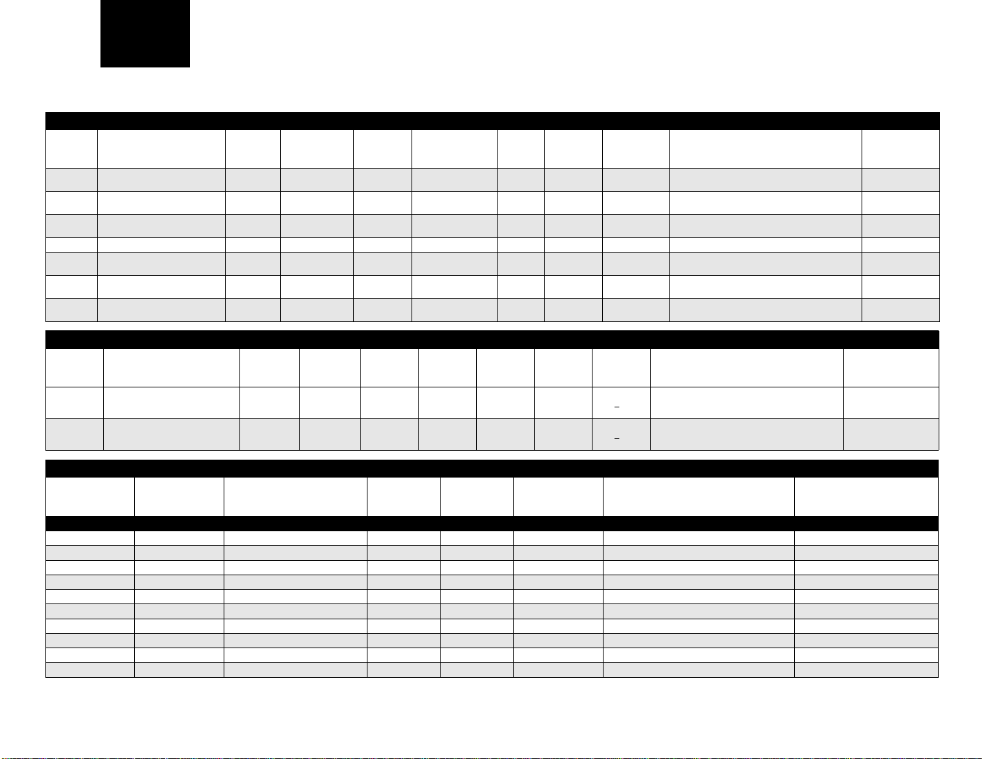
Current 16-Bit
Controller
Family
dsPIC® Digital Signal Controller (DSC) Family
CURRENT 16-BIT CONTROLLER FAMILY PRODUCTS
Product
dsPIC30F General Purpose Family: 30 MIPS, VDD = 2.5V-5.5V, Self-Write Flash, IntOSC = 8 MHz or 32 kHz and nanoWatt Technology
dsPIC30F3014 24 1024 2048 30 40P, 44PT, 44ML ( 8x8) 13 ch — 3 2 2 — — 2 1 1 — — Basic
dsPIC30F4013 48 1024 2048 30 40P, 44PT, 44ML (8x8) 13 ch — 5 4 4 — — 2 1 1 1
dsPIC30F5011 66 1024 4096 52 64PT 16 ch — 5 8 8 — — 2 2 1 2
dsPIC30F5013 66 1024 4096 68 80PT 16 ch — 5 8 8 — — 2 2 1 2
dsPIC30F6011A 132 2048 6144 52 64PF, 64PT 16 ch — 5 8 8 — — 2 2 1 2 — Advanced
dsPIC30F6012A 144 4096 8192 52 64PF, 64PT 16 ch — 5 8 8 — — 2 2 1 2
dsPIC30F6013A 132 2048 6144 68 80PF, 80PT 16 ch — 5 8 8 — — 2 2 1 2 — Advanced
dsPIC30F6014A 144 4096 8192 68 80PF, 80PT 16 ch — 5 8 8 — — 2 2 1 2
dsPIC30F Motor Control and Power Conversion Family: 30 MIPS, VDD = 2.5V-5.5V, Self-Write Flash, IntOSC = 8 MHz or 32 kHz and nanoWatt Technology
dsPIC30F2010 12 1024 512 20 28SO, 28SP, 28MM (6x6) — 6 ch 3 4 2 6 ✓ 111—— Basic
dsPIC30F3010 24 1024 1024 20 28SO, 28SP, 44ML (8x8) — 6 ch 5 4 2 6 ✓ 1 1 1 — — Basic
dsPIC30F4012 48 1024 2048 20 28SO, 28SP, 44ML (8x8) — 6 ch 5 4 2 6 ✓ 1111 — Basic
dsPIC30F3011 24 1024 1024 30 40P, 44PT, 44ML (8x8) — 9 ch 5 4 4 6 ✓ 2 1 1 — — Basic
dsPIC30F4011 48 1024 2048 30 40P, 44PT, 44ML (8x8) — 9 ch 5 4 4 6 ✓ 2111 — Basic
dsPIC30F4012 48 1024 2048 20 28SO, 28SP, 44ML (8x8) — 6 ch 5 4 2 6 ✓ 1 1 1 1 — Basic
dsPIC30F5015 66 1024 2048 52 64PT — 16 ch 5 4 4 8 ✓ 1211 — Basic
dsPIC30F6015 144 4096 8192 52 64PT — 16 ch 5 8 8 8 ✓ 2 2 1 1 — Advanced
dsPIC30F5016 66 1024 2048 68 80PT — 16 ch 5 4 4 8 ✓ 1211 — Basic
dsPIC30F6010A 144 4096 8192 68 80PF, 80PT — 16 ch 5 8 8 8 ✓ 2 2 1 2 — Advanced
dsPIC30F6015 144 4096 8192 52 64PT — 16 ch 5 8 8 8 ✓ 2211 — Advanced
*Contact Microchip Technology Inc. for availability date.
Abbreviations are found on the last page of the Selector Guide.
Program
Memory
(Kbytes)
Data
EEPROM
(Bytes)
RAM
(Bytes)
I/O
Pins
Packages
A/D 12-Bit
200 ksps
A/D 10-Bit
1 Msps
Timer
16-Bit
Input
Cap
Output
Comp/
Std PWM
Motor
Control
PWM
QEI
UART
w/
IrDA
CAN
Codec
Interface
AC97, I2S
AC97, I
AC97, I2S
AC97, I2S
AC97, I2S
2
SPI
C™
®
I
CodeGuard™
2
S
Security
Basic
Advanced
Advanced
Advanced
Advanced
PAGE 6
Page 9
dsPIC® Digital Signal Controller (DSC) Family (continued)
Product
dsPIC30F Sensor Family: 30 MIPS, VDD = 2.5V-5.5V, Self-Write Flash, IntOSC = 8 MHz or 32 kHz and nanoWatt Technology
dsPIC30F2011 12 0 1024 12 18SO, 18P, 28ML (6x6) 8 ch — 3 2 2 — — 1 1 1 — — Basic
dsPIC30F2012 12 0 1024 20 28SO, 28SP, 28ML (6x6) 10 ch — 3 2 2 — — 1 1 1 — — Basic
dsPIC30F3012 24 1024 2048 12 18SO, 18P, 44ML (8x8) 8 ch — 3 2 2 — — 1 1 1 — — Basic
dsPIC30F3013 24 1024 2048 20 28SO, 28SP, 44ML (8x8) 10 ch — 3 2 2 — — 2 1 1 — — Basic
*Contact Microchip Technology Inc. for availability date.
Abbreviations are found on the last page of the Selector Guide.
dsPIC30F SMPS and Digital Power Conversion: 30 MIPS, VDD = 2.5V-5.5V, Self-Write Flash, IntOSC = 8 MHz or 32 kHz and nanoWatt Technology
Product
dsPIC30F1010 6 — 256 21
dsPIC30F2020 12 — 512 21
dsPIC30F2023 12 — 512 35
*Contact Microchip Technology Inc. for availability date.
Abbreviations are found on the last page of the Selector Guide.
Program
Memory
(Kbytes)
Program
Memory
(Kbytes)
Data
EEPROM
(Bytes)
Data
EEPROM
(Bytes)
RAM
(Bytes)
RAM
(Kbytes)
I/O
Pins
I/O
Pins
Packages
Packages
28SP,
28SO,
28MM
28SP,
28SO,
28MM
44PT,
44ML
A/D 12-Bit
200 ksps
A/D
# of
10-bit
2 Msps
S/H
6 ch 2 2 — 1 2 x 2 2 1 1 1 — — Intermediate
8 ch 4 3 1 2 4 x 2 4 1 1 1 — — Intermediate
12 ch 4 3 1 2 4 x 2 4 1 1 1 — — Intermediate
A/D 10-Bit
1 Msps
Timer
16-bit
Input
Cap
Timer
16-Bit
Output
Comp/
Std
PWM
Input
Cap
Output
Comp/
Std PWM
High speed
SMPS PWNM
(1.1 ns
resolution)
Motor
Control
PWM
High
Speed
Analog
Comp
QEI
UART
IrDA
UART
w/
IrDA
SPI
2
C™
I
2
CAN
C™
I
w/
®
SPI
®
CAN
Codec
Interface
Codec
Interface
CodeGuard™
Security
CodeGuard™
Security
Current 16-Bit
Controller
Family
PAGE 7
Page 10

Current 16-Bit
Controller
Family
dsPIC® Digital Signal Controller (DSC) Family (continued)
A/D Config. as
Product
dsPIC33F General Purpose Family: 40 MIPS, VDD = 3.0V-3.6V , Self-Write Flash, IntOSC = 8 MHz or 32 kHz, JTAG/DMA and nanoWatt Technology
dsPIC33FJ64GP201* 12 1 13
dsPIC33FJ64GP202* 12 1 21
dsPIC33FJ64GP206 64 8 53 64PT
dsPIC33FJ64GP306 64 16 53 64PT
dsPIC33FJ64GP310 64 16 85
dsPIC33FJ64GP706 64 16 53 64PT
dsPIC33FJ64GP708 64 16 69 80PT
dsPIC33FJ64GP710 64 16 85
dsPIC33FJ128GP206 128 8 53 64PT
dsPIC33FJ128GP306 128 16 53 64PT
dsPIC33FJ128GP310 128 16 85
dsPIC33FJ128GP706 128 16 53 64PT
dsPIC33FJ128GP708 128 16 69 80PT
NOTE 1: dsPIC33F devices with 2 A/D converters can achieve 2.2 Msps conversion rate.
*Contact Microchip Technology for availability date.
Abbreviations are found on the last page of the Selector Guide.
2: Each A/D configured as 10-bit has 4 S/H. Each A/D configured as 12-bit has 1 S/H.
Program
Memory
(Kbytes)
RAM
(Kbytes)
I/O
Pins
Packages
18P,
18SO
28SP,
28SO,
28ML
100PT ,
100PF
100PT ,
100PF
100PT ,
100PF
10-Bit @
1.1 Msps or
12-Bit @
(1,2)
500 ksps
1 A/D, 6 ch,
4 S/H max.
1 A/D, 10 ch,
4 S/H max.
1 A/D, 18 ch,
4 S/H max.
1 A/D, 18 ch,
4 S/H max.
1 A/D, 32 ch,
4 S/H max.
2 A/D, 18 ch,
8 S/H max.
2 A/D, 24 ch,
8 S/H max
2 A/D, 32 ch,
8 S/H max.
1 A/D, 18 ch,
4 S/H max
1 A/D, 18 ch,
4 S/H max.
1 A/D, 18 ch,
4 S/H max.
2 A/D, 18 ch,
8 S/H max.
2 A/D, 24 ch,
8 S/H max.
Timer
Input
16-Bit
3 4 2 — — 1 1 1 — — — Intermediate
3 4 2 — — 1 1 1 — — — Intermediate
9 8 8 — — 2 2 1 0 1 — Advanced
9 8 8 — — 2 2 2 — 1 — Advanced
9 8 8 — — 2 2 2 0 1 — Advanced
9 8 8 — — 2 2 2 2 1 — Advanced
9 8 8 — — 2 2 2 2 1 — Advanced
9 8 8 — — 2 2 2 2 1 — Advanced
9 8 8 — — 2 2 1 — 1 — Advanced
9 8 8 — — 2 2 2 — 1 — Advanced
9 8 8 — — 2 2 2 — 1 — Advanced
9 8 8 — — 2 2 2 2 1 — Advanced
9 8 8 — — 2 2 2 2 1 — Advanced
Cap
Output
Comp/
Std PWM
Motor
Control
PWM
QEI
UART
w/
IrDA
ECAN™
2
SPI
C™
I
®
Technology
Codec
Interface
PPS
CodeGuard™
Security
PAGE 8
Page 11

dsPIC® Digital Signal Controller (DSC) Family (continued)
A/D Config. as
Product
dsPIC33F General Purpose Family: 40 MIPS, VDD = 3.0V-3.6V , Self-Write Flash, IntOSC = 8 MHz or 32 kHz, JTAG/DMA and nanoWatt Technology (continued)
dsPIC33FJ128GP710 128 16 85
dsPIC33FJ256GP506 256 16 53 64PT
dsPIC33FJ256GP510 256 16 85
dsPIC33FJ256GP710 256 30 85
dsPIC33F Motor Control Family: 40 MIPS, VDD = 3.0V-3.6V, Self-Write Flash, IntOSC = 8 MHz or 32 kHz, JTAG/DMA and nanoWatt Te chnology
dsPIC33FJ12MC201* 12 1 15
dsPIC33FJ12MC202* 12 1 21
dsPIC33FJ64MC506 64 8 53 64PT
dsPIC33FJ64MC508 64 8 69 80PT
dsPIC33FJ64MC510 64 8 85
dsPIC33FJ64MC706 64 16 53 64PT
dsPIC33FJ64MC710 64 16 85
dsPIC33FJ128MC506 128 8 53 64PT
dsPIC33FJ128MC510 128 8 85
NOTE 1: dsPIC33F devices with 2 A/D converters can achieve 2.2 Msps conversion rate.
*Contact Microchip Technology for availability date.
Abbreviations are found on the last page of the Selector Guide.
2: Each A/D configured as 10-bit has 4 S/H. Each A/D configured as 12-bit has 1 S/H.
Program
Memory
(Kbytes)
RAM
(Kbytes)
I/O
Pins
Packages
100PT ,
100PF
100PT ,
100PF
100PT ,
100PF
20SP,
20SO
28SP,
28SO,
28ML
100PT ,
100PF
100PT ,
100PF
100PT ,
100PF
10-Bit @
1.1 Msps or
12-Bit @
(1,2)
500 ksps
2 A/C, 32 ch,
8 S/H max.
1 A/D, 18 ch,
4 S/H max.
1 A/D, 32 ch,
4 S/H max.
2 A/D, 32 ch,
8 S/H max.
1 A/D, 4 ch,
4 S/H max.
1 A/D, 6 ch,
4 S/H max.
1 A/D, 16 ch,
4 S/H max.
1 A/D, 18 ch,
4 S/H max.
1 A/D, 24 ch,
4 S/H max.
2 A/D, 16 ch,
8 S/H max.
2 A/D, 24 ch,
8 S/H max.
1 A/D, 16 ch,
4 S/H max.
1 A/D, 24 ch,
4 S/H max.
Timer
Input
16-Bit
9 8 8 — — 2 2 2 2 1 — Advanced
9 8 8 — — 2 2 2 1 1 — Advanced
9 8 8 — — 2 2 2 1 1 — Advanced
9 8 8 — — 2 2 2 2 1 — Advanced
34 2 6✓ 1 1 1 — — — Intermediate
3 4 2 6 ✓ 1 1 1 — — — Intermediate
98 8 8✓ 222 1 — —Advanced
9 8 8 8 ✓ 2 2 2 1 — — Advanced
98 8 8✓ 222 1 — —Advanced
9 8 8 8 ✓ 2 2 2 1 — — Advanced
98 8 8✓ 222 2 — —Advanced
9 8 8 8 ✓ 2 2 2 1 — — Advanced
98 8 8✓ 222 1 — —Advanced
Cap
Output
Comp/
Std PWM
Motor
Control
PWM
QEI
UART
w/
IrDA
®
SPI
I
2
C™
ECAN™
Technology
Codec
Interface
PPS
CodeGuard™
Security
Current 16-Bit
Controller
Family
PAGE 9
Page 12

Current 16-Bit
Controller
Family
dsPIC® Digital Signal Controller (DSC) Family (continued)
A/D Config. as
Product
dsPIC33F Motor Control Family: 40 MIPS, VDD = 3.0V-3.6V, Self-Write Flash, IntOSC = 8 MHz or 32 kHz, JTAG/DMA and nanoWatt T e chnology (continued)
dsPIC33FJ128MC706 128 16 53 64PT
dsPIC33FJ128MC708 128 16 69 80PT
dsPIC33FJ128MC710 128 16 85
dsPIC33FJ256MC510 256 16 85
dsPIC33FJ256MC710 256 30 85
NOTE 1: dsPIC33F devices with 2 A/D converters can achieve 2.2 Msps conversion rate.
*Contact Microchip Technology for availability date.
Abbreviations are found on the last page of the Selector Guide.
2: Each A/D configured as 10-bit has 4 S/H. Each A/D configured as 12-bit has 1 S/H.
Program
Memory
(Kbytes)
RAM
(Kbytes)
I/O
Pins
Packages
100PT ,
100PF
100PT ,
100PF
100PT ,
100PF
10-Bit @
1.1 Msps or
12-Bit @
(1,2)
500 ksps
2 A/D, 16 ch,
8 S/H max.
2 A/D, 18 ch,
8 S/H max.
2 A/D, 24 ch,
8 S/H max.
1 A/D, 16 ch,
4 S/H max.
2 A/D, 24 ch,
8 S/H max.
Timer
Input
16-Bit
9 8 8 8 ✓ 2 2 2 1 — — Advanced
98 8 8✓ 222 1 — —Advanced
9 8 8 8 ✓ 2 2 2 2 — — Advanced
98 8 8✓ 222 1 — —Advanced
9 8 8 8 ✓ 2 2 2 2 — — Advanced
Cap
Output
Comp/
Std PWM
Motor
Control
PWM
QEI
UART
w/
IrDA
PIC24 16-Bit Micr o co n t ro l ler (MCU) Family
Product
PIC24FJ Family: 16 MIPS, VDD = 2.0V-3.6V, Self-Write Flash, IntOSC = 8 MHz or 32 kHz and nanoWatt Technology
PIC24FJ64GA006 64 8 53 64PT
PIC24FJ64GA008 64 8 69 80PT
PIC24FJ64GA010 64 8 85
PIC24FJ96GA006 96 8 53 64PT
PIC24FJ96GA008 96 8 69 80PT
NOTE: PIC24H devices with 2 A/D converters can achieve 2.2 Msps conversion rate.
*Contact Microchip Technology for availability date.
Abbreviations are found on the last page of the Selector Guide.
Program
Memory
(Kbytes)
RAM
(Kbytes)
I/O
Packages ADC
Pins
100PT ,
100PF
16x10-bit
500 ksps
16x10-bit
500 ksps
16x10-bit
500 ksps
16x10-bit
500 ksps
16x10-bit
500 ksps
Analog
Timers
Comp.
255 5 ✓ 222 —✓ —BasicJTAG
2 5 5 5 ✓ 2 2 2 — ✓ — Basic JTAG
255 5 ✓ 222 —✓ —BasicJTAG
2 5 5 5 ✓ 2 2 2 — ✓ — Basic JTAG
255 5 ✓ 222 —✓ —BasicJTAG
16-Bit
Input
Cap
Output
Comp/PWM
RTCC
UART
w/IrDA
SPI
®
ECAN™
2
SPI
I
C™
®
2
I
C™
Technology
ECAN™
Technology
PMP PPS
Codec
Interface
CodeGuard™
Security
PPS
CodeGuard™
Security
Other Features
PAGE 10
Page 13

PIC24 16-Bit Microcontroller (MCU) Family (continued)
Product
PIC24FJ Family: 16 MIPS, VDD = 2.0V-3.6V, Self-Write Flash, IntOSC = 8 MHz or 32 kHz and nanoWatt Technology (continued)
PIC24FJ96GA010 96 8 85
PIC24FJ128GA006 128 8 53 64PT
PIC24FJ128GA008 128 8 69 80PT
PIC24FJ128GA010 128 8 85
PIC24HJ Family: 40 MIPS, VDD = 3.0V-3.6V, Self-Write Flash, IntOSC = 8 MHz or 32 kHz and nanoWatt Technology
PIC24HJ12GP201* 12 1 13 18P, 18SO
PIC24HJ12GP202* 12 1 21
PIC24HJ64GP206 64 8 53 64PT
PIC24HJ64GP210 64 8 85
PIC24HJ64GP506 64 8 53 64PT
PIC24HJ64GP510 64 8 85
PIC24HJ128GP206 128 8 53 64PT
PIC24HJ128GP210 128 8 85
PIC24HJ128GP306 128 16 53 64PT
NOTE: PIC24H devices with 2 A/D converters can achieve 2.2 Msps conversion rate.
*Contact Microchip Technology for availability date.
Abbreviations are found on the last page of the Selector Guide.
Program
Memory
(Kbytes)
RAM
(Kbytes)
I/O
Packages ADC
Pins
100PT ,
100PF
100PT ,
100PF
28P , 28SO,
28ML
100PT ,
100PF
100PT ,
100PF
100PT ,
100PF
16x10-bit
500 ksps
16x10-bit
500 ksps
16x10-bit
500 ksps
16x10-bit
500 ksps
6x10-bit
1.1 Msps or
12-bit 500 ksps
10x10-bit
1.1 Msps or
12-bit 500 ksps
18x10-bit
1.1 Msps or
12-bit 500 ksps
32x10-bit
1.1 Msps or
12-bit 500 ksps
18x10-bit
1.1 Msps or
12-bit 500 ksps
32x10-bit
1.1 Msps or
12-bit 500 ksps
18x10-bit
1.1 Msps or
12-bit 500 ksps
32x10-bit
1.1 Msps or
12-bit 500 ksps
18x10-bit
1.1 Msps or
12-bit 500 ksps
Analog
Timers
Comp.
2 5 5 5 ✓ 2 2 2 — ✓ — Basic JTAG
255 5 ✓ 222 —✓ —BasicJTAG
2 5 5 5 ✓ 2 2 2 — ✓ — Basic JTAG
255 5 ✓ 222 —✓ —BasicJTAG
— 3 4 2 — 1 1 1 — — ✓ Intermediate
—34 2 —111 ——✓ Intermediate
— 9 8 8 — 2 2 1 — — — Advanced
— 9 8 8 — 2 2 2 — — — Advanced
— 9 8 8 — 2 2 2 1 — — Advanced
— 9 8 8 — 2 2 2 1 — — Advanced
— 9 8 8 — 2 2 2 — — — Advanced
— 9 8 8 — 2 2 2 — — — Advanced
— 9 8 8 — 2 2 2 — — — Advanced
16-Bit
Input
Cap
Output
Comp/PWM
RTCC
UART
w/IrDA
SPI
C™
®
I
Technology
PMP PPS
ECAN™
2
CodeGuard™
Security
Other Features
JTAG, DMA
(8 ch)
JTAG, DMA
(8 ch)
JTAG, DMA
(8 ch)
JTAG, DMA
(8 ch)
JTAG, DMA
(8 ch)
JTAG, DMA
(8 ch)
JTAG, DMA
(8 ch)
Current 16-Bit
Controller
Family
PAGE 11
Page 14

Current 16-Bit
Controller
Family
PIC24 16-Bit Microcontroller (MCU) Family (continued)
PIC24HJ Family: 40 MIPS, VDD = 3.0V-3.6V, Self-Write Flash, IntOSC = 8 MHz or 32 kHz and nanoWatt Technology (continued)
PIC24HJ128GP310 128 16 85
PIC24HJ128GP506 128 8 53 64PT
PIC24HJ128GP510 128 8 85
PIC24HJ256GP206 256 16 53 64PT
PIC24HJ256GP210 256 16 85
PIC24HJ256GP610 256 16 85
*Contact Microchip Technology for availability date.
Abbreviations are found on the last page of the Selector Guide.
Product
NOTE: PIC24H devices with 2 A/D converters can achieve 2.2 Msps conversion rate.
Program
Memory
(Kbytes)
RAM
(Kbytes)
I/O
Packages ADC
Pins
100PT ,
100PF
100PT ,
100PF
100PT ,
100PF
100PT ,
100PF
32x10-bit
1.1 Msps or
12-bit 500 ksps
18x10-bit
1.1 Msps or
12-bit 500 ksps
32x10-bit
1.1 Msps or
12-bit 500 ksps
18x10-bit
1.1 Msps or
12-bit 500 ksps
32x10-bit
1.1 Msps or
12-bit 500 ksps
(2) 32x10-bit
1.1 Msps or
12-bit 500 ksps
Analog
Comp.
— 9 8 8 — 2 2 2 — — — Advanced
— 9 8 8 — 2 2 2 1 — — Advanced
— 9 8 8 — 2 2 2 1 — — Advanced
— 9 8 8 — 2 2 2 — — — Advanced
— 9 8 8 — 2 2 2 2 — — Advanced
— 9 8 8 — 2 2 2 2 — — Advanced
Timers
16-Bit
Input
Cap
Output
Comp/PWM
RTCC
UART
w/IrDA
SPI
I
®
C™
Technology
PMP PPS
ECAN™
2
CodeGuard™
Security
Other Features
JTAG, DMA
(8 ch)
JTAG, DMA
(8 ch)
JTAG, DMA
(8 ch)
JTAG, DMA
(8 ch)
JTAG, DMA
(8 ch)
JTAG, DMA
(8 ch)
PAGE 12
Page 15

FUTURE 16-BIT CONTROLLER FAMIL Y PRODUCTS
dsPIC® Digital Signal Controller (DSC) Family
Product
dsPIC33F General Purpose Family: 40 MIPS, VDD = 3.0V-3.6V , Self-W rite Flash, IntOSC = 8 MHz or 32 kHz and nanoWatt Technology
dsPIC33FJ32GP202 32 2 21
dsPIC33FJ32GP204 32 2 35
dsPIC33FJ32GP302 32 4 21
dsPIC33FJ32GP304 32 4 35
dsPIC33FJ64GP202 64 8 21
dsPIC33FJ64GP204 64 8 35
dsPIC33FJ64GP802 64 16 21
dsPIC33FJ64GP804 64 16 35
dsPIC33FJ128GP202 128 8 21
dsPIC33FJ128GP204 128 8 35
dsPIC33FJ128GP802 128 16 21
dsPIC33FJ128GP804 128 16 35
NOTE 1: dsPIC33F devices with 2 A/D converters can achieve 2.2 Msps conversion rate.
Abbreviations are found on the last page of the Selector Guide.
2: Each A/D configured as 10-bit has 4 S/H. Each A/D configured as 12-bit has 1 S/H.
Program
Memory
(Kbytes)
RAM
(Kbytes)
I/O
Pins
Packages
28SP,
28SO,
28ML
44ML,
44PT
28SP,
28SO,
28ML
44ML,
44PT
28SP,
28SO,
28ML
44ML,
44PT
28SP,
28SO,
28ML
44ML,
44PT
28SP,
28SO,
28ML
44ML,
44PT
28SP,
28SO,
28ML
44ML,
44PT
A/D config as
10-Bit @
1.1 Msps or
12-bit @
(1,2)
500 ksps
1 A/D, 10 ch,
4 S/H max.
1 A/D, 13 ch,
4 S/H max.
1 A/D, 10 ch,
4 S/H max.
1 A/D, 13 ch,
4 S/H max.
1 A/D, 10 ch,
4 S/H max.
1 A/D, 13 ch,
4 S/H max.
1 A/D, 10 ch,
4 S/H max.
1 A/D, 13 ch,
4 S/H max.
1 A/D, 10 ch,
4 S/H max.
1 A/D, 13 ch,
4 S/H max.
1 A/D, 10 ch,
4 S/H max.
1 A/D, 13 ch,
4 S/H max.
Timer
16-Bit
34 2 ——111 — —✓ Intermediate
3 4 2 — — 1 1 1 — — ✓ Intermediate
54 4 ——221 — 1✓ Advanced
5 4 4 — — 2 2 1 — 1 ✓ Advanced
54 4 ——221 — 1✓ Advanced
5 4 4 — — 2 2 1 — 1 ✓
54 4 ——221 1 1✓ Advanced
5 4 4 — — 2 2 1 1 1 ✓
54 4 ——221 — 1✓ Advanced
5 4 4 — — 2 2 1 — 1 ✓
54 4 ——221 1 1✓ Advanced
5 4 4 — — 2 2 1 1 1 ✓
Input
Cap
Output
Comp/
Std PWM
Motor
Control
PWM
QEI
UART
w/
IrDA
SPI
®
I2C™
ECAN™
Technology
Codec
Interface
PPS
CodeGuard™
Security
Advanced
Advanced
Advanced
Advanced
Future 16-Bit
Controller
Family
PAGE 13
Page 16

Future 16-Bit
Controller
Family
dsPIC® Digital Signal Controller (DSC) Family (continued)
dsPIC33F Motor Control Family: 40 MIPS, VDD = 3.0V-3.6V, Self-Write Flash, IntOSC = 8 MHz or 32 kHz and nanoWatt Technology
dsPIC33FJ32MC202 32 2 21
dsPIC33FJ32MC204 32 2 35
dsPIC33FJ32MC302 32 4 21
dsPIC33FJ32MC304 32 4 35
dsPIC33FJ64MC202 64 8 21
dsPIC33FJ64MC204 64 8 35
dsPIC33FJ64MC802 64 16 21
dsPIC33FJ64MC804 64 16 35
dsPIC33FJ128MC202 128 8 21
dsPIC33FJ128MC204 128 8 35
dsPIC33FJ128MC802 128 16 21
dsPIC33FJ128MC804 128 16 35
Abbreviations are found on the last page of the Selector Guide.
Product
NOTE 1: dsPIC33F devices with 2 A/D converters can achieve 2.2 Msps conversion rate.
2: Each A/D configured as 10-bit has 4 S/H. Each A/D configured as 12-bit has 1 S/H.
Program
Memory
(Kbytes)
RAM
(Kbytes)
I/O
Pins
Packages
28SP,
28SO,
28ML
44ML,
44PT
28SP,
28SO,
28ML
44ML,
44PT
28SP,
28SO,
28ML
44ML,
44PT
28SP,
28SO,
28ML
44ML,
44PT
28SP,
28SO,
28ML
44ML,
44PT
28SP,
28SO,
28ML
44ML,
44PT
A/D config as
10-Bit @
1.1 Msps or
12-bit @
(1,2)
500 ksps
1 A/D, 6 ch,
4 S/H max
1 A/D, 9 ch,
4 S/H max
1 A/D, 6 ch,
4 S/H max
1 A/D, 9 ch,
4 S/H max
1 A/D, 6 ch,
4 S/H max
1 A/D, 9 ch,
4 S/H max
1 A/D, 6 ch,
4 S/H max
1 A/D, 9 ch,
4 S/H max
1 A/D, 6 ch,
4 S/H max
1 A/D, 9 ch,
4 S/H max
1 A/D, 6 ch,
4 S/H max
1 A/D, 9 ch,
4 S/H max
Input
Cap
Output
Comp/
Std PWM
Timer
16-Bit
34 2 81111 — —✓ Intermediate
3 4 2 8 1 1 1 1 — — ✓ Intermediate
54 4 82221 — —✓ Advanced
5 4 4 8 2 2 2 1 — — ✓ Advanced
54 4 82221 — —✓ Advanced
5 4 4 8 2 2 2 1 — — ✓ Advanced
54 4 82221 1 —✓ Advanced
5 4 4 8 2 2 2 1 1 — ✓ Advanced
54 4 82221 — —✓ Advanced
5 4 4 8 2 2 2 1 — — ✓ Advanced
54 4 82221 1 —✓ Advanced
5 4 4 8 2 2 2 1 1 — ✓ Advanced
Motor
Control
PWM
QEI
UART
w/
IrDA
SPI
®
I2C™
ECAN™
Technology
Codec
Interface
PPS
CodeGuard™
Security
PAGE 14
Page 17

PIC24 16-Bit Micr o co n t ro l ler (MCU) Family
Product
PIC24FJ Family: 16 MIPS, VDD = 2.0V-3.6V, Self-Write Flash, IntOSC = 8 MHz or 32 kHz and nanoWatt Technology
PIC24FJ32GA002 32 8 21 28SP, 28SO, 28ML
PIC24FJ64GA002 64 8 21 28SP, 2 8 SO , 28 ML
PIC24FJ32GA004 32 8 35 44ML, 44PT
PIC24FJ64GA004 64 8 35 44ML, 44PT
PIC24HJ Family: 40 MIPS, VDD = 3.0V-3.6V, Self-Write Flash, IntOSC = 8 MHz or 32 kHz and nanoWatt Technology
PIC24HJ32GP202 32 2 21
PIC24HJ32GP204 32 2 35 44ML, 44PT
PIC24HJ32GP302 32 4 21 28SP, 28SO, 28ML
PIC24HJ32GP304 32 4 35 44ML, 44PT
PIC24HJ64GP202 64 8 21 28SP, 28SO, 28ML
PIC24HJ64GP204 64 8 35 44ML, 44PT
PIC24HJ64GP502 64 8 21 28SP, 28SO, 28ML
PIC24HJ64GP504 64 8 35 44ML, 44PT
PIC24HJ128GP202 128 8 21 28SP , 28SO, 28ML
PIC24HJ128GP204 128 8 35 44ML, 44PT
PIC24HJ128GP502 128 8 21 28SP , 28SO, 28ML
PIC24HJ128GP504 128 8 35 44ML, 44PT
Abbreviations are found on the last page of the Selector Guide.
Program
Memory
(Kbytes)
RAM
(Kbytes)
I/O
Pins
Packages ADC
10x10-bit
500 ksps
10x10-bit
500 ksps
13x10-bit
500 ksps
13x10-bit
500 ksps
28SP, 28SO,
28SS, 28ML
10x10-bit
1.1 Msps or
12-bit 500 ksps
13x10-bit
1.1 Msps or
12-bit 500 ksps
10x10-bit
1.1 Msps or
12-bit 500 ksps
13x10-bit
1.1 Msps or
12-bit 500 ksps
10x10-bit
1.1 Msps or
12-bit 500 ksps
13x10-bit
1.1 Msps or
12-bit 500 ksps
10x10-bit
1.1 Msps or
12-bit 500 ksps
13x10-bit
1.1 Msps or
12-bit 500 ksps
10x10-bit
1.1 Msps or
12-bit 500 ksps
13x10-bit
1.1 Msps or
12-bit 500 ksps
10x10-bit
1.1 Msps or
12-bit 500 ksps
13x10-bit
1.1 Msps or
12-bit 500 ksps
Analog
Timers
16-Bit
Input
Cap
Comp
255 5 ✓ 222 — ✓✓ Basic JTAG
2 5 5 5 ✓ 2 2 2 — ✓ ✓ Basic JTAG
255 5 ✓ 222 — ✓✓ Basic JTAG
2 5 5 5 ✓ 2 2 2 — ✓ ✓ Basic JTAG
—34 2 —111 ——✓ Intermediate JTAG, DMA (8ch)
— 3 4 2 — 1 1 1 — — ✓ Intermediate JT AG, DMA (8ch)
254 4 ✓ 221 — ✓✓ Advanced JTAG, DMA (8ch)
2 5 4 4 ✓ 2 2 1 — ✓ ✓ Advanced JTAG, DMA (8ch)
254 4 ✓ 221 — ✓✓ Advanced JTAG, DMA (8ch)
2 5 4 4 ✓ 2 2 1 — ✓ ✓ Advanced JTAG, DMA (8ch)
254 4 ✓ 221 1 ✓✓ Advanced JTAG, DMA (8ch)
2 5 4 4 ✓ 2 2 1 1 ✓ ✓ Advanced JTAG, DMA (8ch)
254 4 ✓ 221 — ✓✓ Advanced JTAG, DMA (8ch)
2 5 4 4 ✓ 2 2 1 — ✓ ✓ Advanced JTAG, DMA (8ch)
254 4 ✓ 221 1 ✓✓ Advanced JTAG, DMA (8ch )
2 5 4 4 ✓ 2 2 1 1 ✓ ✓ Advanced JTAG, DMA (8ch)
Output
Comp/PWM
RTCC
UART
w/IrDA
SPI
C™
®
I
Technology
PMP PPS
ECAN™
2
CodeGuard™
Security
Other Features
PAGE 15
Future 16-Bit
Controller
Family
Page 18

Current Analog/
Interface
Family
Lead-free versions of many devices are currently offered. Check Microchip’s web site for availability.
CURRENT ANALOG/INTERFACE PRODUCTS
THERMAL MANAGEMENT PRODUCTS – Temperature Sensors
Part #
Logic Output Temperature Sensors
TC6501 ±0.5 ±3 -55 to +125 +2.7 to +5.5 40 Cross to MAX6501, Open-drain 5-Pin SOT-23A
TC6502 ±0.5 ±3 -55 to +125 +2.7 to +5.5 40 Cross to MAX6502, Push-pull 5-Pin SOT-23A
TC6503 ±0.5 ±3 -55 to +125 +2.7 to +5.5 40 Cross to MAX6503, Open-drain 5-Pin SOT-23A
TC6504 ±0.5 ±3 -55 to +125 +2.7 to +5.5 40 Cross to MAX6504, Push-pull 5-Pin SOT-23A
TC620 ±1 ±3 -40 to +125 +4.5 to +18 400 Two resistor-programmable trip points 8-Pin PDIP, 8-Pin SOIC
TC621 Note 1 Note 1 -40 to +85 +4.5 to +18 400
TC622 ±1 ±5 -40 to +125 +4.5 to +18 600
TC623 ±1 ±3 -40 to +125 +2.7 to +4.5 250 Two resistor-programmable trip points 8-Pin PDIP, 8-Pin SOIC
TC624 ±1 ±5 -40 to +125 +2.7 to +4.5 300 Dual output, resistor-programmable trip points 8-Pin PDIP, 8-Pin SOIC
Voltage Output Temperature Sensors
MCP9700 +
MCP9701 +1 +4 -10 to +125 +3.1 to +5.5 12
MCP9700A +1+2 -40 to +125 +2.3 to +5.5 12
MCP9701A +1 +2 -40 to +125 +3.1 to +5.5 12
TC1046 ±0.5 ±2 -40 to +125 +2.7 to +4.4 60
TC1047 ±0.5 ±2 -40 to +125 +2.7 to +4.4 60
TC1047A ±0.5 ±2 -40 to +125 +2.5 to +5.5 60
Serial Output Temperature Sensors
MCP9800 ±0.5 ±1 -55 to +125 +2.7 to +5.5 400
MCP9801 ±0.5 ±1 -55 to +125 +2.7 to +5.5 400
NOTE 1: These devices use an external temperature sensor. Accuracy of the total solution is a function of the accuracy of the external sensor.
2: TCN75 idle current is 250 μA. This device also has a Software Shutdown mode that reduces supply current to <1 μA.
3: MCP9805 max. accuracy measured at 85°C.
Typical Accuracy
(°C)
1+4 -40 to +125 +2.3 to +5.5 12
Maximum Accuracy
@ 25°C (°C)
Maximum
Temperature Range
(°C)
CC Range (V)
V
Maximum Supply
Current (µA)
Features Packages
Requires external thermistor,
resistor-programmab l e trip poin ts
Dual output, TO-220 for heat sink mounting,
resistor-programmab l e trip poin ts
®
Linear Active Thermistor
slope: 10 mV/°C
Linear Active Thermistor® IC, Temperature
slope: 19.53 mV/°C, cross to MAX6612
Linear Active Thermistor
slope: 10 mV/°C
Linear Active Thermistor® IC, Temperature
slope: 19.53 mV/°C, cross to MAX6612
High precision temperature-to-voltage
converter, 6.25 mV/°C
High precision temperature-to-voltage
converter, 10 mV/°C
High precision temperature-to-voltage
converter, 10 mV/°C
SMbus/I2C™ compatible interface, 0.0625°C
to 0.5°C adj. resolution, power-saving oneshot temperature measurement
2
SMbus/I
C™ compatible interface, 0.0625°C
to 0.5°C adj. resolution, power-saving oneshot temperature measurement, multi-drop
capability
IC, Temperature
®
IC, Temperature
8-Pin PDIP, 8-Pin SOIC
8-Pin PDIP, 8-Pin SOIC, 5-Pin TO-220
3-pin TO-92, 5-pin SC-70
3-pin TO-92, 5-pin SC-70
3-pin TO-92, 5-pin SC-70
3-pin TO-92, 5-pin SC-70
3-Pin SOT-23B
3-Pin SOT-23B
3-Pin SOT-23B
5-Pin SOT-23
8-Pin MSOP, 8-pin SOIC
PAGE 16
Page 19

THERMAL MANAGEMENT PRODUCTS – Temperature Sensors (continued)
Part #
Serial Output Temperature Sensors (continued)
MCP9802 ±0.5 ±1 -55 to +125 +2.7 to +5.5 400
MCP9803 ±0.5 ±1 -55 to +125 +2.7 to +5.5 400
MCP9805 +0.5
MCP98242 +
TC77 ±0.5 ±1 -55 to +125 +2.7 to +5.5 400
TC72 ±0.5 ±1 -55 to +125 +2.65 to +5.5 400
TC74 ±0.5 ±2 -40 to +125 +2.7 to +5.5 350
TCN75A ±0.5 ±2 -40 to +125 +2.7 to +5.5 500
TCN75 ±0.5 ±2 -55 to +125 +2.7 to +5.5
NOTE 1: These devices use an external temperature sensor. Accuracy of the total solution is a function of the accuracy of the external sensor.
2: TCN75 idle current is 250 μA. This device also has a Software Shutdown mode that reduces supply current to <1 μA.
3: MCP9805 max. accuracy measured at 85°C.
Typical Accuracy
(°C)
0.5
Maximum Accuracy
@ 25°C (°C)
(3)
+1
(3)
1
+
Maximum
Temperature Range
(°C)
-20 to +125 +3.0 to +3.6 400
-20 to +125 +3.0 to +3.6 400
CC Range (V)
V
Maximum Supply
Current (µA)
(2)
1,000
SMbus/I2C™ compatible interface with time
out, 0.0625°C to 0.5°C adj. resolution, powersaving one-shot temperatur e mea surement
SMbus/I
out, 0.0625°C to 0.5°C adj. resolution, powersaving one-shot temperatur e mea sure me nt,
multi-drop capability
JEDEC compatible register set, SMbus/I2C™
compatible interface, programmable, shutdown modes and EVENT output
Same temperature sensor as MCP9805 plus
integrated DDR2 Serial Presence Detect
EEPROM
SPI compatible interface, 0.0625°C
temperature resolution
SPI compatible interface, power-saving oneshot temperature measurement, 0.25°C
temperature resolution
SMbus/I2C™ compatible interface, 1°C
temperature resolution
SMbus/I
saving one-shot temperatur e mea sure me nt,
multi-drop capability, 0.0625°C to 0.5°C
adjustable temperature resolution
SMbus/I2C™ compatible interface, multi-drop
capability, interrupt output, 0.5°C temperature
resolution
Features Packages
5-Pin SOT-23
2
C™ compatible interface with time
2
C™ compatible interface, power-
8-Pin MSOP, 8-Pin SOIC
8-Pin TSSOP, 8-Pin 2x3 DFN
8-Pin TSSOP, 8-Pin 2x3 DFN
5-Pin SOT-23A, 8-Pin SOIC
8-Pin MSOP, 8-Pin 3x3 DFN
5-Pin SOT-23A, 5-Pin TO-220
8-Pin SOIC, 8-Pin MSOP
8-Pin MSOP, 8-Pin SOIC
THERMAL MANAGEMENT PRODUCTS – Brushless DC Fan Controllers and Fan Fault Detectors
Part # Description
TC642 Fan Manager Note 1 Note 1 -40 to +85 +3.0 to +5.5 1,000
TC642B Fan Manager Note 1 Note 1 -40 to +85 +3. 0 to +5.5 400
TC646 Fan Manager Note 1 Note 1 -40 to +85 +3.0 to +5.5 1,000
NOTE 1: These devices use an external temperature sensor. Accuracy of the total solution is a function of the accuracy of the external sensor.
Typ ical Accuracy
(°C)
Maximum Accuracy
@ 25°C (°C)
Maximum
Temperature Range
(°C)
Vcc Range (V)
Maximum Supply
Current (μA)
Current Analog/
Interface
Family
Features Packages
FanSense™ Fan Monitor,
minimum fan speed control
FanSense™ Fan Monitor,
minimum fan speed control, fan
auto-restart
FanSense™ Fan Monitor,
auto-shutdown
8-Pin PDIP, 8-Pin SOIC,
8-Pin MSOP
8-Pin PDIP, 8-Pin SOIC,
8-Pin MSOP
8-Pin PDIP, 8-Pin SOIC,
8-Pin MSOP
PAGE 17
Page 20
Current Analog/
Interface
Family
THERMAL MANAGEMENT PRODUCTS – Brushless DC Fan Controllers and Fan Fault Detectors (continued)
Part # Description
TC646B Fan Manager Note 1 Note 1 -40 to +85 +3. 0 to +5.5 400
TC647 Fan Manager Note 1 Note 1 -40 to +85 +3.0 to +5.5 1,000
TC647B Fan Manager Note 1 Note 1 -40 to +85 +3. 0 to +5.5 400
TC648 Fan Manager Note 1 Note 1 -40 to +85 +3.0 to +5.5 1,000
TC648B Fan Manager Note 1 Note 1 -40 to +85 +3. 0 to +5.5 400
TC649 Fan Manager Note 1 Note 1 -40 to +85 +3.0 to +5.5 1,000
TC649B Fan Manager Note 1 Note 1 -40 to +85 +3. 0 to +5.5 400
TC650 Fan Manager ±1 ±3 -40 to +125 +2.8 to +5.5 90 Over-temperature alert 8-Pin MSOP
TC651 Fan Manager ±1 ±3 -40 to +125 +2.8 to +5.5 90
TC652 Fan Manager ±1 ±3 -40 to +125 +2.8 to +5.5 90
TC653 Fan Manager ±1 ±3 -40 to +125 +2.8 to +5.5 90
TC654
TC655
TC664
TC665
TC670
NOTE 1: These devices use an external temperature sensor. Accuracy of the total solution is a function of the accuracy of the external sensor.
Dual SMbus Fan Manager
Dual SMbus Fan Manager
Single SMbus Fan
Manager
Single SMbus Fan
Manager
Predictive Fan Fault
Detector
Typ ical Accuracy
(°C)
Note 1 Note 1 -40 to +85 +3.0 to +5.5 320
Note 1 Note 1 -40 to +85 +3.0 to +5.5 320
Note 1 Note 1 -40 to +85 +3.0 to +5.5 320
Note 1 Note 1 -40 to +85 +3.0 to +5.5 320
N/A N/A -40 to +85 +3.0 to +5.5 150
Maximum Accuracy
@ 25°C (°C)
Maximum
Temperature Range
(°C)
Vcc Range (V)
Maximum Supply
Current (μA)
Features Packages
FanSense™ Fan Monitor,
auto-shutdown, fan auto-restart
FanSense™ Fan Monitor,
minimum fan speed control
FanSense™ Fan Monitor,
minimum fan speed control, fan
auto-restart
Over-temperature alert,
auto-shutdown
Over-temperature alert,
auto-shutdown, fan auto-restart
FanSense™ Fan Monitor,
auto-shutdown
FanSense™ Fan Monitor,
auto-shutdown, fan auto-restart
Over-temperature alert,
auto-shutdown
FanSense™ Fan Monitor,
over-temperature alert
FanSense™ Fan Monitor,
over-temperature alert,
auto-shutdown
FanSense™ Fan Monitor,
RPM data
FanSense™ Fan Monitor, RPM
data, over-temperature alert
FanSense™ Fan Monitor,
RPM data
FanSense™ Fan Monitor, RPM
data, over-temperature alert
FanSense™ Fan Monitor,
programmable threshold
8-Pin PDIP, 8-Pin SOIC,
8-Pin MSOP
8-Pin PDIP, 8-Pin SOIC,
8-Pin MSOP
8-Pin PDIP, 8-Pin SOIC,
8-Pin MSOP
8-Pin PDIP, 8-Pin SOIC,
8-Pin MSOP
8-Pin PDIP, 8-Pin SOIC,
8-Pin MSOP
8-Pin PDIP, 8-Pin SOIC,
8-Pin MSOP
8-Pin PDIP, 8-Pin SOIC,
8-Pin MSOP
8-Pin MSOP
8-Pin MSOP
8-Pin MSOP
10-Pin MSOP
10-Pin MSOP
10-Pin MSOP
10-Pin MSOP
6-Pin SOT-23
POWER MANAGEMENT – Voltage References
Part # Vcc Range (V) Output Voltage (V) Max. Load Current (mA)
MCP1525 2.7 to 5.5 2.5 ±2 ±1 50 100 3-Pin TO-92, 3-Pin SOT-23B
MCP1541 4.3 to 5.5 4.096 ±2 ±1 50 100 3-Pin TO-92, 3-Pin SOT-23B
Initial Accuracy
(max.%)
Temperature
Coefficient (ppm/°C)
Max. Supply Current
(μA @ 25°C)
Packages
PAGE 18
Page 21

POWER MANAGEMENT – Linear Regulators
Part #
50 mA to 250 mA Low-Dropout Linear Regulators
TC2014 6.0 1.8, 2.7, 2.8, 3.0, 3.3 50 -40 to +125 55 45 ±0.4 Shutdown, Reference bypass input 5-Pin SOT-23A
TC1014 6.0 1.8, 2.5, 2.7, 2.8, 2.85, 3.0, 3.3, 3.6, 4.0, 5.0 50 -40 to +125 50 85 ±0.5 Shutdown, Reference bypass input 5-Pin SOT-23A
TC2054 6.0 1.8, 2.7, 2.8, 3.0, 3.3 50 -40 to +125 55 45 ±0.4 Shutdown, Error output 5-Pin SOT-23A
TC1054 6.0 1.8, 2.5, 2.7, 2.8, 2.85, 3.0, 3.3, 3.6, 4.0, 5.0 50 -40 to +125 50 85 ±0.5 Shutdown, Error output 5-Pin SOT-23A
TC1070 6.0 1.23 → V
TC1072 6.0 2.5, 2.7, 2.8, 2.85, 3.0, 3.3, 3.6, 4.0, 5.0 50 -40 to +125 50 85 ±0.5
TC1223 6.0 2.5, 2.7, 2.8, 3.0, 3.3, 3.6, 4.0, 5.0 50 -40 to +125 50 85 ±0.5 Shutdown 5-Pin SOT-23A
TC1016 6.0 1.8, 2.7, 2.8, 3.0 80 -40 to +125 50 150 ±0.5 Shutdown 5-Pin SC-70
TC2015 6.0 1.8, 2.7, 2.8, 3.0, 3.3 100 -40 to +125 55 90 ±0.4 Shutdown, Reference bypass input 5-Pin SOT-23A
TC1015 6.0 1.8, 2.5, 2.7, 2.8, 2.85, 3.0, 3.3, 3.6, 4.0, 5.0 100 -40 to +125 50 180 ±0.5 Shutdown, Reference bypass input 5-Pin SOT-23A
TC2055 6.0 1.8, 2.7, 2.8, 3.0, 3.3 100 -40 to +125 55 90 ±0.4 Shutdown, Error output 5-Pin SOT-23A
TC1055 6.0 1.8, 2.5, 2.7, 2.8, 2.85, 3.0, 3.3, 3.6, 4.0, 5.0 100 -40 to +125 50 180 ±0.5 Shutdown, Error output 5-Pin SOT-23A
TC1071 6.0 1.23 → V
TC1073 6.0 2.5, 2.7, 2.8, 2.85, 3.0, 3.3, 3.6, 4.0, 5.0 100 -40 to +125 50 180 ±0.5
TC1224 6.0 2.5, 2.7, 2.8, 3.0, 3.3, 3.6, 4.0, 5.0 100 -40 to +125 50 180 ±0.5 Shutdown 5-Pin SOT-23A
TC1188 6.0 1.8, 2.8, 2.84, 3.15 120 -40 to +125 50 130 ±0.5 Shutdown 5-Pin SOT-23A
TC1189 6.0 1.8, 2.8, 2.84, 3.15 120 -40 to +125 50 130 ±0.5 Shutdown 5-Pin SOT-23A
TC2185 6.0 1.8, 2.7, 2.8, 3.0, 3.3 150 -40 to +125 55 140 ±0.4 Shutdown, Reference bypass input 5-Pin SOT-23A
TC1185 6.0 1.8, 2.5, 2.7, 2.8, 2.85, 3.0, 3.3, 3.6, 4.0, 5.0 150 -40 to +125 50 270 ±0.5 Shutdown, Reference bypass input 5-Pin SOT-23A
TC2186 6.0 1.8, 2.7, 2.8, 3.0, 3.3 150 -40 to +125 55 140 ±0.4 Shutdown, Error output 5-Pin SOT-23A
TC1186 6.0 1.8, 2.5, 2.7, 2.8, 2.85, 3.0, 3.3, 3.6, 4.0, 5.0 150 -40 to +125 50 270 ±0.5 Shutdown, Error output 5-Pin SOT-23A
TC1187 6.0 1.23 → VIN 150 -40 to +125 50 270 — Shutdown, Adjustable 5-Pin SOT-23A
TC1017 6.0 1.8, 2.6, 2.7, 2.8, 2.85, 2.9, 3.3, 3.4 150 -40 to +125 53 285 +
MCP1700 6.0 1.2, 1.8, 2.5, 3.0, 3.3, 5.0 250 -40 to +125 1.0 300 +0.4
MCP1701 10 1.8, 2.5, 3.0, 3.3, 5.0 250 -40 to +85 1.1 380 +
MCP1702 12 1.2, 1.5, 1.8, 2.5, 2.8, 3.0, 3.5, 4.0, 5.0 250 -40 to +125 2 650 +0.4
NOTE 1: Depending on external transistor configuration.
Max. Input
Voltage (V)
2: Each channel (for Dual and Quad LDOs).
3: LDOs with shutdown (except Power-Management Combination Products as indicated) have typical shutdown currents of 0.05 μA.
Output Voltage (V)
IN 50 -40 to +125 50 85 — Shutdown, Adjustable 5-Pin SOT-23A
IN 100 -40 to +125 50 180 — Shutdown, Adjustable 5-Pin SOT-23A
Output
Current (mA)
Junction
Temperature
Range (°C)
Typical
Active
Current (μA)
Typical Dropout
Voltage @ Max.
OUT (mV)
I
Typical Output
Voltage
Accuracy (%)
Shutdown, Reference bypass input,
Error output
Shutdown, Reference bypass input,
Error output
0.5 Shutdown 5-Pin SOT-23A, 5-Pin SC-70
1.0 μF ceramic cap stable,
Short-circuit protection
0.5 10V max. input voltage
Ultra-low ground current, 12V VIN
max.
Features Packages
6-Pin SOT-23A
6-Pin SOT-23A
3-Pin TO-92, 3-Pin SOT-23A,
3-Pin SOT-89
3-Pin SOT-23A, 3-Pin SOT-89,
3-Pin TO-92
3-Pin SOT-23A, 3-Pin SOT-89,
3-Pin TO-92
Current Analog/
Interface
Family
PAGE 19
Page 22

Current Analog/
Interface
Family
POWER MANAGEMENT – Linear Regulators (continued)
(1)
Typical Output
Voltage
Accuracy (%)
Shutdown, Reference bypass input,
Error output
Shutdown, Reference bypass input,
Adjustable
Shutdown, Reference bypass input,
Error output
Shutdown, Reference bypass input,
Error output
Shutdown, Reference bypass input,
Error output
Ceramic output capacitor stable,
Shutdown, Cdelay, Power Good
Ceramic output capacitor stable,
Shutdown, Cdelay, Power Good
Ceramic output capacitor stable,
Shutdown, Power Good
±2.0 Shutdown, External transistor 5-Pin SOT-23A
Shutdown, Reference bypass input,
LDO plus Reset output
±0.5
Dual LDO plus Reset output,
Shutdown, Reference bypass,
Voltage detect
Features Packages
8-Pin MSOP, 8-Pin SOIC
8-Pin MSOP, 8-Pin SOIC
3-Pin TO-220, 3-Pin DDPAK,
3-Pin SOT-223
8-Pin SOIC, 5-Pin TO-220,
5-Pin DDPAK
8-Pin SOIC
3-Pin TO-220, 3-Pin DDPAK,
3-Pin SOT-223
8-Pin SOIC, 5-Pin TO-220,
5-Pin DDPAK
8-Pin 3x3 DFN, 8-Pin SOIC
8-Pin 3x3 DFN, 8-Pin SOIC
5-Pin DDPAK, 5-Pin TO-220
8-Pin MSOP
8-Pin MSOP, 8-Pin 3x3 DFN
PAGE 20
Part #
300 mA Low Dropout Linear Regulators
TC1107 6.0 2.5, 2.7, 2.8, 3.0, 3.3, 5.0 300 -40 to +125 50 240 ±0.5 Shutdown, Reference bypass input 8-Pin MSOP, 8-Pin SOIC
TC1108 6.0 2.5, 2.7, 2.8, 3.0, 3.3, 5.0 300 -40 to +125 50 240 ±0.5 3-Pin SOT-223
TC1173 6.0 2.5, 2.7, 2.8, 3.0, 3.3, 5.0 300 -40 to +125 50 240 ±0.5
TC1174 6.0 1.23 → VIN 300 -40 to +125 50 240 —
TC1269 6.0 2.5, 2.8, 3.0, 3.3, 5.0 300 -40 to +125 50 240 ±0.5 Shutdown, Reference bypass input 8-Pin MSOP
500 mA to 800 mA Low Dropout Linear Regulators
TC1262 6.0 2.5, 2.8, 3.0, 3.3, 5.0 500 -40 to +125 80 350 ±0.5
TC1263 6.0 2.5, 2.8, 3.0, 3.3, 5.0 500 -40 to +125 80 350 ±0.5
TC1268 6.0 2.5 500 -40 to +125 80 350 ±0.5
TC1264 6.0 1.8, 2.5, 3.0, 3.3 800 -40 to +125 80 450 ±0.5
TC1265 6.0 1.8, 2.5, 3.0, 3.3 800 -40 to +125 80 450 ±0.5
TC2117 6.0 1.8, 2.5, 3.0, 3.3 800 -40 to +125 80 600 ±0.5 3-Pin SOT-223, 3-Pin DDPAK
1A and Above Low Dropout Linear Regulators
MCP1726 6.0
MCP1727 6.0
MCP1827 6.0
MCP1827S 6.0 Fixed: 5, 3.3, 3, 2.5, 1.8, 1.2, 0.8 1500 -40 to +125 140 330 ±0.5 Ceramic output capacitor stable 3-Pin DDPAK, 3-Pin TO-220
Application Specific Low Dropout Linear Regulators
TC1266 6.0 3.3 200 -5 to +70 230 200 ±1.0 PCI compliant 8-Pin SOIC, 8-Pin MSOP
TC1267 6.0 3.3 400 -5 to +70 230 300 ±1.0 PCI compliant 5-Pin DDPAK
TC57 8 2.5, 3.0, 3.3
TC59 -10 -3.0, -5.0 100 -40 to +85 3 380 ±0.5 Negative LDO 3-Pin SOT-23A
Power Management Combination Products
TC1300
TC1301A
NOTE 1: Depending on external transistor configuration.
Max. Input
Voltage (V)
(3)
(3)
6.0 2.5, 2.7, 2.8, 2.85, 3.0, 3.3 300 -40 to +125 80 210 ±0.5
6.0
2: Each channel (for Dual and Quad LDOs).
3: LDOs with shutdown (except Power-Management Combination Products as indicated) have typical shutdown currents of 0.05 μA.
Output Voltage (V)
Fixed: 5, 3.3, 3, 2.5, 1.8, 1.2, 0.8
Adjustable: 0.8 to 5.0
Fixed: 5, 3.3, 3, 2.5, 1.8, 1.2, 0.8
Adjustable: 0.8 to 5.0
Fixed: 5, 3.3, 3, 2.5, 1.8, 1.2, 0.8
Adjustable: 0.8 to 5.0
LDO1: 1.5-3.3
LDO2: 1.5-3.3
Output
Current (mA)
1000 -40 to +125 140 300 ±0.4
1500 -40 to +125 140 330 ±0.5
1500 -40 to +125 140 330 ±0.5
(1)
4,000
LDO1: 300
LDO2: 150
Junction
Temperature
Range (°C)
-40 to +85 50
-40 to +125 103
Typical
Active
Current (μA)
Typical Dropout
Voltage @ Max.
OUT (mV)
I
100
LDO1: 104
LDO2: 150
Page 23

POWER MANAGEMENT – Linear Regulators (continued)
Part #
Power-Management Combination Products (continued)
TC1301B
TC1302A
TC1302B
TC1305 6.0 2.5, 2.8, 3.0
TC1306 6.0 1.8, 2.8, 3.0
TC1307
NOTE 1: Depending on external transistor configuration.
Max. Input
Voltage (V)
(3)
(3)
(3)
(3)
6.0
6.0
6.0
6.0 1.8, 2.5, 2.8, 3.0
2: Each channel (for Dual and Quad LDOs).
3: LDOs with shutdown (except Power-Management Combination Products as indicated) have typical shutdown currents of 0.05 μA.
Output Voltage (V)
LDO1: 1.5-3.3
LDO2: 1.5-3.3
LDO1: 1.5-3.3
LDO2: 1.5-3.3
LDO1: 1.5-3.3
LDO2: 1.5-3.3
Output
Current (mA)
LDO1: 300
LDO2: 150
LDO1: 300
LDO2: 150
LDO1: 300
LDO2: 150
(2)
150
(2)
150
(2)
150
Junction
Temperature
Range (°C)
-40 to +125 114
-40 to +125 103
-40 to +125 114
-40 to +125 120 240 ±0.5
-40 to +125 120 240 ±0.5
-40 to +125 220 200 ±0.5
Typical
Active
Current (μA)
Typical Dropout
Voltage @ Max.
OUT (mV)
I
LDO1: 104
LDO2: 150
LDO1: 104
LDO2: 150
LDO1: 104
LDO2: 150
Typical Output
Voltage
Accuracy (%)
±0.5
±0.5
±0.5
Features Packages
Dual LDO plus Reset, per channel
output shutdown, Reference bypass
Dual LDO, Output shutdown
reference bypass, Voltage detect
Dual LDO, per channel output shutdown, Reference bypass
Dual LDO plus Reset output,
Reference bypass input, Shutdown,
Select Mode™ selectable output
voltages
Dual LDO plus Reset output,
Shutdown, Select Mode™
selectable output voltages
Quad LDO plus Reset output,
Shutdown, Select Mode™
selectable output voltage
8-Pin MSOP, 8-Pin 3x3 DFN
8-Pin MSOP, 8-Pin 3x3 DFN
8-Pin MSOP, 8-Pin 3x3 DFN
10-Pin MSOP
8-Pin MSOP
16-Pin QSOP
POWER MANAGEMENT – Switching Regulators
Part # Description
MCP1601 Synchronous Buck Regulator 2.7 to 5.5 0.9V to VIN -40 to +85 PFM/PWM/LDO 750
MCP1602
MCP1612
MCP1650 Step-up DC/DC Controller 2.7 to 5.5
MCP1651 Step-up DC/DC Controller 2.7 to 5.5
MCP1652 Step-up DC/DC Controller 2.7 to 5.5
MCP1653 Step-up DC/DC Controller 2.7 to 5.5
TC105 Step-down DC/DC Controller 2.2 to 10 3.0, 3.3, 5.0 -40 to +85 PFM/PWM 300 57 1,000 Low-Power Shutdown mode 5-Pin SOT-23A
TC120
Synchronous Buck DC/DC
Regulator
Synchronous Buck DC/DC
Regulator
Step-down Regulator/Controller
Combination
Input
Voltage
Range (V)
2.7 to 5.5 0.8 to 4.5 -40 to +85 PFM/PWM 2000 35 500
2.7 to ViN 0.8 to 5.5 -40 to +85
1.8 to 10 3.0, 3.3, 5.0 -40 to +85 PFM/PWM 300 52 2,000 Soft-start, Low-Power Shutdown mode 8-Pin SOP
Output Voltage
(V)
2.5 to ext. tx
limited
2.5 to ext. tx
limited
2.5 to ext. tx
limited
2.5 to ext. tx
limited
Operating
Temperature
Range (°C)
-40 to +125
-40 to +125
-40 to +125
-40 to +125
Control Scheme
Constant frequency
PWM
Constant frequency,
2 fixed DC
Constant frequency,
2 fixed DC
Constant frequency,
2 fixed DC
Constant frequency,
2 fixed DC
Switching
Frequency
(kHz)
1400 10,000 1000
750 120 560/440
750 120 560/440
750 120 560/440
750 120 560/440
Typical
Active
Current (μA)
825 (PWM)
125 (PFM)
Output Current
(mA)
500 UVLO, Auto-switching, LDO 8-Pin MSOP
PFM, PWM auto-switching, UVLO, soft start,
Power Good indicator
Overall efficiency >94% soft start, overtemperature and over-current protection
2 duty cycles for min. and max. loads, shutdown
control, UVLO, soft start
2 duty cycles for min. and max. loads, shutdown
control, low battery detect, UVLO, soft start
2 duty cycles for min. and max. loads, shutdown
control, Power Good indicator, UVLO, soft start
2 duty cycles for min. and max. loads, shutdown
control, low battery detect, Power Good indicator,
UVLO, soft start
Features Packages
10-Pin MSOP, 10Pin 3x3 DFN
8-Pin MSOP,
8-Pin 3x3 DFN
8-Pin MSOP
8-Pin MSOP
8-Pin MSOP
10-Pin MSOP
Current Analog/
Interface
Family
PAGE 21
Page 24
Current Analog/
Interface
Family
POWER MANAGEMENT – Switching Regulators (continued)
Part # Description
TC125 Step-up DC/DC Regulator 0.9 to 10 3.0, 3.3, 5.0 -40 to +85 PFM 100 20 80
TC126 Step-up DC/DC Regulator 0.9 to 10 3.0, 3.3, 5.0 -40 to +85 PFM 100 20 80
TC115 Step-up DC/DC Regulator 0.9 to 10 3.0, 3.3, 5.0 -40 to +85 PFM/PWM 100 80 140
TC110 Step-up DC/DC Controller 2.0 to 10 3.0, 3.3, 5.0 -40 to +85 PFM/PWM 100/300 50/120 300 Soft-start, Low-Power Shutdown mode 5-Pin SOT-23A
TC1303
TC1304
TC1313
Synchronous Buck Regulator,
LDO w/Power Good
Synchronous Buck Regulator,
LDO
Synchronous Buck Regulator,
LDO
Input
Voltage
Range (V)
2.7 to 5.5
2.7 to 5.5
2.7 to 5.5
Output Voltage
(V)
DC/DC: 0.8 to 4.5
LDO: 1.5 to 3.3
DC/DC: 0.8 to 4.5
LDO: 1.5 to 3.3
DC/DC: 0.8 to 4.5
LDO: 1.5 to 3.3
POWER MANAGEMENT – PWM Controllers
Part # Description
MCP1630
MCP1630V
High-speed PWM to use with PIC
MCUs
High-speed PWM to use with PIC®
MCUs
Input Voltage
Range (V)
®
2.7 to 5.5
2.7 to 5.5
Output
Voltage (V)
SS + 0.2V
V
VDD – 0.2V
VSS + 0.2V
VDD – 0.2V
Operating
Temperature
Range (°C)
-40 to +85 PFM/PWM 2000 65/600
-40 to +85 PFM/PWM 2000 65/600
-40 to +85 PFM/PWM 2000 65/600
Operating
Temperature
Range (°C)
to
-40 to +125
to
-40 to +125
Control Scheme
Control
Scheme
Cycle-byCycle DC
control
Cycle-byCycle DC
control
Switching
Frequency
Switching
Frequency
(kHz)
1000 2.5 +10 UVLO, current sense to VEXT, response <25 ns 8-Pin MSOP
1000 2.5 +10 Voltage mode and Average Current mode 8-Pin MSOP
(kHz)
Typical
Active
Current (μA)
Typical
Active
Supply (μA)
Output Current
(mA)
DC/DC: 500 mA
LDO: 300 mA
DC/DC: 500 mA
LDO: 300 mA
DC/DC: 500 mA
LDO: 300 mA
Output
Current (mA)
Features Packages
Low-Power Shutdown mode. Not recommended
for new designs
Feedback voltage sensing. Not recommended for
new designs
Feedback voltage sensing, Low-Power
Shutdown mode
PFM/PWM auto-switching, Power Good output
PFM/PWM auto-switching, Power sequencing
PFM/PWM auto-switching
Features Packages
5-Pin SOT-23A
5-Pin SOT-23A
5-Pin SOT-89
10-Pin MSOP,
10-Pin 3x3 DFN
10-Pin MSOP,
10-Pin 3x3 DFN
10-Pin MSOP,
10-Pin 3x3 DFN
POWER MANAG EMENT – Charge Pu mp DC-to-DC Con verters
Part #
Inverting or Doubling Charge Pumps
TC1044S 1.5 to 12 V
TC7660 1.5 to 10 VOUT = -VIN or VOUT = 2 VIN -40 to +85 180 20 10 kHz oscillator 8-Pin PDIP , 8-Pin SOIC
TC7660H 1.5 to 10 V
TC7660S 1.5 to 12 VOUT = -VIN or VOUT = 2 VIN -40 to +85 160 20 45 kHz oscillator, Boost mode 8-Pin PDIP, 8-Pin SOIC
TC7662B 1.5 to 15 V
TC1219 1.5 to 5.5 VOUT = -VIN or VOUT = 2 VIN -40 to +85 115 25 12 kHz oscillator, Low-Power Shutdown mode 6-Pin SOT-23A
TC1220 1.5 to 5.5 V
TC1221 1.8 to 5.5 VOUT = -VIN or VOUT = 2 VIN -40 to +85 600 25 Shutdown, 125 kHz oscillator 6-Pin SOT-23A
TC1222 1.8 to 5.5 V
TCM828 1.5 to 5.5 VOUT = -VIN or VOUT = 2 VIN -40 to +85 90 25 12 kHz oscillator 5-Pin SOT-23A
NOTE 1: Measured at V
Input Voltage Range
(V)
DD = 5.0V at 25°C and no load.
Output Voltage (V)
OUT = -VIN or VOUT = 2 VIN -40 to +85 160 20 85 kHz oscillator, Boost mode 8-Pin PDIP, 8-Pin SOIC
OUT = -VIN or VOUT = 2 VIN -40 to +85 1,000 20 120 kHz oscillator 8-Pin PDIP, 8-Pin SOIC
OUT = -VIN or VOUT = 2 VIN -40 to +85 180 20 35 kHz oscillator, Boost mode 8-Pin PDIP, 8-Pin SOIC
OUT = -VIN or VOUT = 2 VIN -40 to +85 325 25 35 kHz oscillator, Low-Power Shutdown mode 6-Pin SOT-23A
OUT = -VIN or VOUT = 2 VIN -40 to +85 2,800 25 Shutdown, 750 kHz oscillator 6-Pin SOT-23A
Operating
Temperature
Range (°C)
Maximum Input
(1)
(μA)
Current
Typical Active
Output Current (mA)
Features Packages
PAGE 22
Page 25
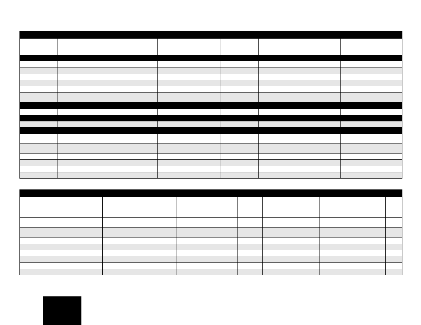
POWER MANAGEMENT – Charge Pump DC-to-DC Co nverters (continued)
Part #
Inverting or Doubling Charge Pumps (continued)
TCM829 1.5 to 5.5 V
TC1240 2.5 to 4.0 VOUT = 2 VIN -40 to +85 900 40 Shutdown, 160 kHz osc ill ato r 6-Pin SOT-23A
TC1240A 2.5 to 5.5 V
TC7662A 3 to 18 VOUT = -VIN or VOUT = 2 VIN -40 to +85 200 40 12 kHz oscillator 8-Pin PDIP
TC962 3 to 18 V
TC1121 2.4 to 5.5 VOUT = -VIN or VOUT = 2 VIN -40 to +85 100 100 Low-Power Shutdown mode
Multi-Function Charge Pumps
TCM680 2.0 to 5.5 V
Inverting and Doubling Charge Pumps
TC682 2.4 to 5.5 VOUT = -2 VIN -40 to +85 400 10 12 kHz oscillator 8-Pin PDIP, 8-Pin SOIC
Regulated Charge Pumps
MCP1252
MCP1253
MCP1256 1.8 to 3.6 3.3 -40 to +85 100 100 Power Good, Sleep mode 10-Pin MSOP, 10-Pin 3x3 DFN
MCP1257 1.8 to 3.6 3.3 -40 to +85 100 100 Sleep mode, low battery indication 10-Pin MSOP, 10-Pin 3x3 DFN
MCP1258 1.8 to 3.6 3.3 -40 to +85 100 100 Power Good output, input/output bypass 10-Pin MSOP, 10-Pin 3x3 DFN
MCP1259 1.8 to 3.6 3.3 -40 to +85 100 100 Low battery indication, input/output bypass 10-Pin MSOP, 10-Pin 3x3 DFN
NOTE 1: Measured at V
Input Voltage Range
(V)
2.1/2.7 to 5.5
2.0 to 5.5
2.1/2.7 to 5.5
2.0 to 5.5
DD = 5.0V at 25°C and no load.
Output Voltage (V)
OUT = -VIN or VOUT = 2 VIN -40 to +85 260 25 35 kHz oscillator 5-Pin SOT-23A
OUT = 2 VIN -40 to +85 900 40 Shutdown, 160 kHz oscillator 6-Pin SOT-23A
OUT = -VIN or VOUT = 2 VIN -40 to +85 200 80 8-Pin PDIP, 16-Pin SOIC
OUT = ±2 VIN -40 to +85 1,000 ±10 Generates ±6V from +3V or ±10V from +5V 8-Pin PDIP, 8-Pin SOIC
Selectable 3.3V or 5.0V or
Adjustable 1.5V to 5.5V
Selectable 3.3V or 5.0V or
Adjustable 1.5V to 5.5V
Operating
Temperature
Range (°C)
-40 to +85 120 120 mA for V
-40 to +85 120 120 mA for VIN>3.0V Power Good output, 1 MHz oscillator 8-Pin MSOP
Maximum Input
(1)
(μA)
Current
Typical Active
Output Current (mA)
IN>3.0V Power Good output, 650 kHz oscillator 8-Pin MSOP
Features Packages
8-Pin MSOP, 8-Pin PDIP,
8-Pin SOIC
POWER MANAGEMENT – CPU/System Supervisors
CC Range
Part #
MCP102 1.0 to 5.5 -40 to +125 4.63, 4.38, 3.08, 2.93, 2.63, 2.32, 1.9 Active-Low CMOS Push-Pull 120 1
MCP103 1.0 to 5.5 -40 to +125 4.63, 4.38, 3.08, 2.93, 2.63, 2.32, 1.9 Active-Low CMOS Push-Pull 120 1 Max. 809 Pinout
TCM809 1.2 to 5.5 -40 to +85 4.63, 4.38, 4.00, 3.08, 2.93, 2.63, 2.32 Active-Low CMOS Push-Pull 240 12 3-Pin SOT-23B, 3-Pin SC-70 N/A
TC1270 1.2 to 5.5 -40 to +85 4.63, 4.38, 3.08, 2.93, 2.63, 1.75 Active-Low CMOS Push-Pull 280 7 Manual Reset 4-Pin SOT-143 N/A
TCM811 1.0 to 5.5 -40 to +85 4.63, 4.38, 3.08, 2.93, 2.63, 1.75 Active-Low CMOS Push-Pull 280 6 Manual Reset 4-Pin SOT-143 N/A
MCP100 1.0 to 5.5 -40 to +85 4.72, 4.62, 4.47, 4.37, 3.075, 2.92, 2.62 Active-Low CMOS Push-Pull 350 45 3-Pin TO-92, 3-Pin SOT-23B D, H
MCP809 1.0 to 5.5 -40 to +85 4.72, 4.62, 4.47, 4.37, 3.075, 2.92, 2.62 Active-Low CMOS Push-Pull 350 45 3-Pin SOT-23B N/A
TCM810 1.2 to 5.5 -40 to +85 4.63, 4.38, 3.08, 2.93, 2.63, 2.32 Active-High CMOS Push-Pull 240 12 3-Pin SOT-23B, 3-Pin SC-70 N/A
V
(V)
Operating
Temperature Range
(°C)
Nominal Reset Voltage (V) Reset Type Output
Typical
Reset Pulse
Width (ms)
Typical
Supply
Current
(μA)
Additional Features Packages
3-Pin SOT-23B, 3-Pin SC-70,
3-Pin TO-92
3-Pin SOT-23B, 3-Pin SC-70,
3-Pin TO-92
Bond
Options
N/A
N/A
Current Analog/
Interface
Family
PAGE 23
Page 26
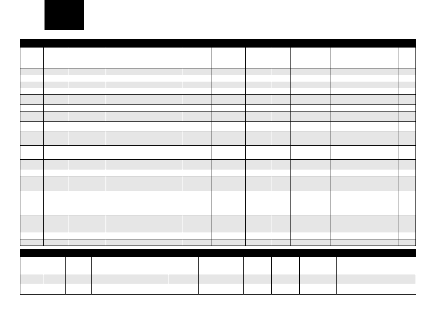
Current Analog/
Interface
Family
POWER MANAGEMENT – CPU/System Supervisors (continued)
CC Range
Part #
TC1271 1.2 to 5.5 -40 to +85 4.63, 4.38, 3.08, 2.93, 2.63, 1.75 Active-High CMOS Push-Pull 280 7 Manual Reset 4-Pin SOT-143 N/A
TCM812 1.1 to 5.5 -40 to +85 4.63, 4.38, 3.08, 2.93, 2.63, 1.75 Active-High CMOS Push-Pull 280 6 Manual Reset 4-Pin SOT-143 N/A
MCP101 1.0 to 5.5 -40 to +85 4.72, 4.62, 4.47, 4.37, 3.075, 2.92, 2.62 Active-High CMOS Push-Pull 350 45 3-Pin TO-92, 3-Pin SOT-23B D, H
MCP810 1.0 to 5.5 -40 to +85 4.72, 4.62, 4.47, 4.37, 3.075, 2.92, 2.62 Active-High CMOS Push-Pull 350 45 3-Pin SOT-23B N/A
MCP121 1.0 to 5.5 -40 to +125 1.9, 2.32, 2, 63, 2.93, 3.08, 4.38, 4.63 Active-Low Open-Drain 120 1
MCP120 1.0 to 5.5 -40 to +85 4.72, 4.62, 4.47, 4.37, 3.075, 2.92, 2.62 Active-Low Open-Drain 350 45 3-Pin TO-92, 3-Pin SOT-23, 8-Pin SOIC D, G, H
MCP131 1.0 to 5.5 -40 to +125 1.9, 2.32, 2, 63, 2.93, 3.08, 4.38, 4.63 Active-Low Open-Drain 120 1
MCP130 1.0 to 5.5 -40 to +85 4.72, 4.62, 4.47, 4.37, 3.075, 2.92, 2.62 Active-Low
MCP1316 1.0 to 5.5 -40 to +125 2.9, 4.6 Active-Low CMOS Push-Pull 200 5
MCP1317 1.0 to 5.5 -40 to +125 2.9, 4.6 Active-High CMOS Push-Pull 200 5
MCP1318 1.0 to 5.5 -40 to +125 4.6 Active-Low/High CMOS Push-Pull 200 5
MCP1319 1.0 to 5.5 -40 to +125 4.6 Active-Low/High CMOS Push-Pull 200 1 Manual reset 5-Pin SOT-23 N/A
MCP1320 1.0 to 5.5 -40 to +125 2.9, 4.6 Active-Low Open-Drain 200 5
MCP1321 1.0 to 5.5 -40 to +125 4.6 Active-Low
MCP1322 1.0 to 5.5 -40 to +125 4.6 Active-High
TC1232 4.5 to 5.5 -40 to +85 4.62, 4.37 Active-Low/High Open-Drain 610 50 Watchdog Timer 8-Pin PDIP, 8-Pin SOIC, 16-Pin SOIC N/A
TC32M 4.5 to 5.5 -40 to +85 4.5 Active-Low Open-Drain 700 50 Watchdog Timer 3-Pin TO-92, 3-Pin SOT-223 N/A
V
(V)
Operating
Temperature Range
(°C)
Nominal Reset Voltage (V) Reset Type Output
Open-Drain w/
5 kOhm Pull-up
Open-Drain/CMOS
Push-Pull
Open-Drain/CMOS
Push-Pull
Typical
Reset Pulse
Width (ms)
350 45 3-Pin TO-92, 3-Pin SOT-23, 8-Pin SOIC D, F, H
200 5
200 1
Typical
Supply
Current
(μA)
Additional Features Packages
3-Pin SOT-23B, 3-Pin SC-70,
3-Pin TO-92
100kΩ Internal Pull-up
Resistor
Watchdog Input (WDI),
Time-out = 1.6 sec.,
Manual reset
Watchdog Input (WDI),
Time-out = 1.6 sec.,
Manual reset
Watchdog Input (WDI),
Time-out = 1.6 sec.
Watchdog Input (WDI),
Time-out = 1.6 sec.,
Manual Reset
Watchdog Input (WDI),
Time-out = 1.6 sec.,
Manual Reset
(Active-Low OpenDrain, Active-High
Push-Pull)
Manual Reset, two
Reset outputs (Active-
Low Open-Drain,
Active-High Push-Pull)
3-Pin SOT-23B, 3-Pin SC-70,
3-Pin TO-92
5-Pin SOT-23 N/A
5-Pin SOT-23 N/A
5-Pin SOT-23 N/A
5-Pin SOT-23 N/A
5-Pin SOT-23 N/A
5-Pin SOT-23 N/A
Bond
Options
N/A
N/A
POWER MANAGEMENT – Voltage Detectors
(V)
Operating
Temperature
Range (°C)
Nominal Reset Voltage (V) Reset Type Output
CC Range
Part #
MCP11 1 1.0 to 5.5 -40 to +125 4.63, 4.38, 3.08, 2.93, 2.63, 2.32, 1.90 Active-Low Open-Drain — 1
MCP112 1.0 to 5.5 -40 to +125 4.63, 4.38, 3.08, 2.93, 2.63, 2.32, 1.90 Active-Low CMOS Push-Pull — 1
V
Minimum
Reset Pulse
Width (ms)
Typical Supply
Current (μA)
Features Packages
3-Pin SOT-23B, 3-Pin TO-92, 3-Pin SC-70,
3-Pin SOT-89
3-Pin SOT-23B, 3-Pin TO-92, 3-Pin SC-70,
3-Pin SOT-89
PAGE 24
Page 27

POWER MANAGEMENT – Voltage Detectors (continued)
(V)
Operating
Temperature
Range (°C)
Nominal Reset Voltage (V) Reset Type Output
CMOS Push-Pull or
Open-Drain
CMOS Push-Pull or
Open-Drain
CC Range
Part #
TC51 0.7 to 10 -40 to +85 3.0, 2.7, 2.2 Active-Low Open-Drain 50 1 Reset delay 3-Pin SOT-23A
TC52 1.5 to 10 -40 to +85 4.5/2.7, 3.0/2.7 Active-Low Open-Drain — 2 Dual channel 5-Pin SOT-23A
TC53 1.5 to 10 -40 to +85 2.9, 2.7, 2.2 Active-Low
TC54 0.7 to 10 -40 to +85 4.3, 4.2, 3.0, 2.9, 2.7, 2.1, 1.4 Active-Low
V
Minimum
Reset Pulse
Width (ms)
Typical Supply
Current (μA)
— 1 5-Pin SOT-23A
— 1 3-Pin SOT-23A, 3-Pin SOT-89, 3-Pin TO-92
Features Packages
POWER MANAGEMENT – Power MOSFET Drivers
Part # Configuration
Low-Side Drivers, 0.5A to 1.2A Peak Output Current
TC1410 Single, Inverting -40 to +85 0.5 22/22 16 30/30 8-Pin PDIP, 8-Pin SOIC, 8-Pin MSOP
TC1410N Single, Non-inverting -40 to +85 0.5 22/22 16 30/30 8-Pin PDIP, 8-Pin SOIC, 8-Pin MSOP
TC1411 Single, Inverting -40 to +85 1 11/11 16 30/30 8-Pin PDIP, 8-Pin SOIC, 8-Pin MSOP
TC1411N Single, Non-inverting -40 to +85 1 11/11 16 30/30 8-Pin PDIP, 8-Pin SOIC, 8-Pin MSOP
TC1426 Dual, Inverting 0 to +70 1.2 18/18 16 75/75 8-Pin PDIP, 8-Pin SOIC
TC1427 Dual, Non-inverting 0 to +70 1.2 18/18 16 75/75 8-Pin PDIP, 8-Pin SOIC
TC1428 Dual, Inverting and Non-inverting 0 to +70 1.2 18/18 16 75/75 8-Pin PDIP, 8-Pin SOIC
TC4467 Quad, Inverting -40 to +85 1.2 15/15 18 40/40 14-Pin PDIP, 16-Pin SOIC (W)
TC4468 Quad, Non-inverting -40 to +85 1.2 15/15 18 40/40 14-Pin PDIP, 16-Pin SOIC (W)
TC4469 Quad, Non-inverting -40 to +85 1.2 15/15 18 40/40 14-Pin PDIP, 16-Pin SOIC (W)
Low-Side Drivers, 1.5A Peak Output Current
TC4403
TC4426A Dual, Inverting -40 to +125 1.5 9/9 18 30/30 8-Pin PDIP, 8-Pin SOIC, 8-Pin DFN
TC4427A Dual, Non-inverting -40 to +125 1.5 9/9 18 30/30 8-Pin PDIP, 8-Pin SOIC, 8-Pin DFN
TC4428A Dual, Inverting and Non-inverting -40 to +125 1.5 9/9 18 30/30 8-Pin PDIP, 8-Pin SOIC, 8-Pin DFN
TC4426 Dual, Inverting -40 to +125 1.5 10/10 18 20/40 8-Pin PDIP, 8-Pin SOIC, 8-Pin DFN, 8-Pin MSOP
TC4427 Dual, Non-inverting -40 to +125 1.5 10/10 18 20/40 8-Pin PDIP, 8-Pin SOIC, 8-Pin DFN, 8-Pin MSOP
TC4428 Dual, Inverting and Non-inverting -40 to +125 1.5 10/10 18 20/40 8-Pin PDIP, 8-Pin SOIC, 8-Pin DFN, 8-Pin MSOP
TC426 Dual, Inverting -40 to +85 1.5 15/10 18 50/75 8-Pin PDIP, 8-Pin SOIC
TC427 Dual, Non-inverting -40 to +85 1.5 15/10 18 50/75 8-Pin PDIP, 8-Pin SOIC
TC428 Dual, Inverting and Non-inverting -40 to +85 1.5 15/10 18 50/75 8-Pin PDIP, 8-Pin SOIC
TC4404 Dual, Inverting -40 to +85 1.5 10/10 18 15/32 8-Pin PDIP, 8-Pin SOIC
TC4405 Dual, Non-inverting -40 to +85 1.5 10/10 18 15/32 8-Pin PDIP, 8-Pin SOIC
NOTE 1: *t
Single, Non-inverting Floating Load
Driver
D1 = delay time from input low-to-high transition to output transition. tD2 = delay time from input high-to-low transition to output transition.
Operating
Temperature
Range (°C)
-40 to +85 1.5 5/5 18 33/38 8-Pin PDIP
Peak Output
Current (A)
Output Resistance
H/RL)
(R
(Max. Ω @ 25°C)
Max. Supply Voltage
(V)
Input/Output Delay (td1, td2)
(ns)
(1)
Packages
Current Analog/
Interface
Family
PAGE 25
Page 28
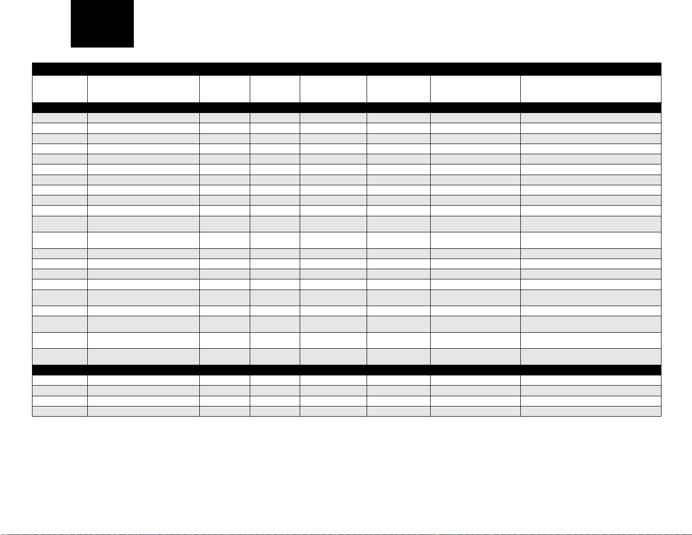
Current Analog/
Interface
Family
POWER MANAGEMENT – Power MOSFET Drivers (continued)
Part # Configuration
Low-Side Drivers, 2.0A to 12.0A Peak Output Current
TC1412 Single, Inverting -40 to +85 2 6/6 16 35/35 8-Pin PDIP, 8-Pin SOIC, 8-Pin MSOP
TC1412N Single, Non-inverting -40 to +85 2 6/6 16 35/35 8-Pin PDIP, 8-Pin SOIC, 8-Pin MSOP
TC1413 Single, Inverting -40 to +85 3 4/4 16 35/35 8-Pin PDIP, 8-Pin SOIC, 8-Pin MSOP
TC1413N Single, Non-inverting -40 to +85 3 4/4 16 35/35 8-Pin PDIP, 8-Pin SOIC, 8-Pin MSOP
TC4423A Dual, Inverting -40 to +125 3 3 (typ)/4 (typ) 18 40 (typ)/40 (typ) 8-Pin PDIP, 8-Pin SOIC, 8-Pin DFN
TC4424A Dual, Non-inverting -40 to +125 3 3 (typ)/4 (typ) 18 40 (typ)/40 (typ) 8-Pin PDIP, 8-Pin SOIC, 8-Pin DFN
TC4425A D ual , Inver ti ng and No n-in ver t ing -40 to +125 3 3 (typ)/4 (typ) 18 40 (typ)/40 (typ) 8-Pin PDIP, 8-Pin SOIC, 8-Pin DFN
TC4423 Dual, Inverting -40 to +125 3 5/5 18 33/38 8-Pin PDIP, 16-Pin SOIC (W), 8-Pin DFN
TC4424 Dual, Non-inverting -40 to +125 3 5/5 18 33/38 8-Pin PDIP, 16-Pin SOIC (W), 8-Pin DFN
TC4425 Dual, Inverting and Non-inverting -40 to +125 3 5/5 18 33/38 8-Pin PDIP, 16-Pin SOIC (W), 8-Pin DFN
MCP1406 Single, Inverting -40 to +125 6 1.8 (typ)/2.0 (typ) 18 30/30
MCP1407 Single, Non-inverting -40 to +125 6 1.8 (typ)/2.0 (typ) 18 30/30
TC429 Single, Inverting -40 to +85 6 2.5/2.5 18 53/60 8-Pin PDIP, 8-Pin DFN, 8-Pin SOIC
TC4420 Single, Non-inverting -40 to +125 6 2.8/2.5 18 55/55 8-Pin PDIP, 8-Pin SOIC, 5-Pin TO-220, 8-Pin DFN
TC4429 Single, Inverting -40 to +125 6 2.8/2.5 18 55/55 8-Pin PDIP, 8-Pin SOIC, 5-Pin TO-220, 8-Pin DFN
TC4421 Single, Inverting -40 to +125 9 1.4 (typ)/1.7 18 30/33 8-Pin PDIP, 5-Pin TO-220, 8-Pin DFN
TC4421A Single, Inverting -40 to +125 9 1.25 (typ)/1.5 18 38/42
TC4422 Single, Non-inverting -40 to +125 9 1.4 (typ)/1.7 18 30/33 8-Pin PDIP, 5-Pin TO-220, 8-Pin DFN
TC4422A Single, Non-inverting -40 to +125 9 1.25 (typ)/1.5 18 38/42
TC4451 Single, Inverting -40 to +125 12 0.6 (typ)/1.5 18 15/15
TC4452 Single, Non-inverting -40 to +125 12 0.6 (typ)/1.5 18 15/15
High-Side/Low-Side Drivers
TC4626 Single, Inverting -40 to +85 1.5 15/10 6 35/45 8-Pin PDIP, 16-Pin SOIC (W)
TC4627 Single, Non-inverting -40 to +85 1.5 15/10 6 35/45 8-Pin PDIP, 16-Pin SOIC (W)
TC4431 Single, Inverting -40 to +85 1.5 10/10 30 62/78 8-Pin PDIP, 8-Pin SOIC
TC4432 Single, Non-inverting -40 to +85 1.5 10/10 30 62/78 8-Pin PDIP, 8-Pin SOIC
NOTE 1: *t
D1 = delay time from input low-to-high transition to output transition. tD2 = delay time from input high-to-low transition to output transition.
Operating
Temperature
Range (°C)
Peak Output
Current (A)
Output Resistance
H/RL)
(R
(Max. Ω @ 25°C)
Max. Supply Voltage
(V)
Input/Output Delay (td1, td2)
(ns)
(1)
5-Pin TO-220, 8-Pin PDIP, 8-Pin 6x5 DFN, 8-Pin
SOIC
5-Pin TO-220, 8-Pin PDIP, 8-Pin 6x5 DFN, 8-Pin
SOIC
8-Pin PDIP, 8-Pin SOIC, 5-Pin TO-220,
8-Pin 6x5 DFN
8-Pin PDIP, 8-Pin SOIC, 5-Pin TO-220,
8-Pin 6x5 DFN
8-Pin SOIC, 8-Pin PDIP, 8-Pin 6x5 DFN,
5-Pin TO-220, 5-Pin DDPAK
8-Pin SOIC, 8-Pin PDIP, 8-Pin 6x5 DFN,
5-Pin TO-220, 5-Pin DDPAK
Packages
PAGE 26
Page 29
POWER MANAG E M ENT – Battery Chargers
Part # Mode Cell Type # of Cells VCC Range (V) Cell Voltage (V)
High-Side/Low-Side Drivers (continued)
MCP73826 Linear Li-Ion/Li-Polymer 1 4.5 to 5.5 4.1, 4.2 N/A +
MCP73827 Linear Li-Ion/Li-Polymer 1 4.5 to 5.5 4.1, 4.2 N/A +1.0 Ext
MCP73828 Linear Li-Ion/Li Polymer 1 4.5 to 5.5 4.1, 4.2 N/A +
MCP73831 Linear Li-Ion/Li-Polymer 1 3.7 to 6.0 4.2, 4.35, 4.4, 4.5 500 +0.75 Int
MCP73832 Linear Li-Ion/Li-Polymer 1 3.7 to 6.0 4.2, 4.35, 4.4, 4.5 500 +
MCP73833 Linear Li-Ion/Li-Polymer 1 3.7 to 6.0 4.2, 4.35, 4.4, 4.5 1000 +0.75 Int
MCP73834 Linear Li-Ion/Li-Polymer 1 3.7 to 6.0 4.2, 4.35, 4.4, 4.5 1000 +
MCP73841 Linear Li-Ion/Li-Polymer 1 4.5 to 12 4.1, 4.2 N/A +0.5 Ext
MCP73842 Linear Li-Ion/Li-Polymer 2 8.7 to 12 8.2, 8.4 N/A +
MCP73843 Linear Li-Ion/Li-Polymer 1 4.5 to 12 4.1, 4.2 N/A +0.5 Ext
MCP73844 Linear Li-Ion/Li-Polymer 2 8.7 to 12 8.2, 8.4 N/A +
MCP73853 Linear Li-Ion/Li-Polymer 1 4.5 to 5.5 4.1, 4.2 500 +0.5 Int
MCP73855 Linear Li-Ion/Li-Polymer 1 4.5 to 5.5 4.1, 4.2 500 +
MCP73861 Linear Li-Ion/Li-Polymer 1 4.5 to 12 4.1, 4.2 1000 +0.5 Int
MCP73862 Linear Li-Ion/Li-Polymer 2 8.7 to 12 8.2, 8.4 1000 +
MCP73863 Linear Li-Ion/Li-Polymer 1 4.5 to 12 4.1, 4.2 1000 +0.5 Int
MCP73864 Linear Li-Ion/Li-Polymer 2 8.7 to 12 8.2, 8.4 1000 +
Max. Charging
Current (mA)
Max. Voltage
Regulation (%)
1.0 Ext Small size, charge current set by external FET 6-Pin SOT-23
1.0 Ext
0.75 Int
0.75 Int
0.5 Ext
0.5 Ext
0.5 Int
0.5 Int
0.5 Int
Int/Ext FET Features Packages
Mode indicator, Charge Current monitor, charge
current set by external FET
Temperature monitor, charge current set by external FET
UVLO, Thermal regulation, Programmable charge
current, tri-state STAT pin
UVLO, Thermal regulation, Programmable charge
current, open-drain STAT pin
UVLO, Thermal regulation, Thermistor input, LDO
Test mode, Multiple V
Power Good output
UVLO, Thermal regulation, Thermistor input, LDO
Test mode, Multiple VREG outputs, Safety timer,
Timer enable input
Safety charge timers, T emperature monitor, charge
current set by external FET
Safety charge timers, T emperature monitor, charge
current set by external FET
Safety charge timers, charge current set by
external FET
Safety charge timers, charge current set by
external FET
USB control, Safety charge timers, Temperature
monitor, Thermal regulation
USB control, Safety charge timers, Thermal
regulation
Safety charge timers, Temperature monitor, Thermal regulation, flashing STAT1 output on charge
complete
Safety charge timers, Temperature monitor,
Thermal regulation, hi-Z STAT1 output on charge
complete
Safety charge timers, Temperature monitor,
Thermal regulation, hi-Z STAT1 output on charge
complete
Safety charge timers, Temperature monitor,
Thermal regulation, hi-Z STAT1 output on charge
complete
REG outputs, Safety timer,
8-Pin MSOP
8-Pin MSOP
5-Pin SOT-23,
8-Pin 2x3 DFN
5-Pin SOT-23,
8-Pin 2x3 DFN
10-Pin 3x3 DFN,
10-Pin MSOP
10-Pin 3x3 DFN,
10-Pin MSOP
10-Pin MSOP
10-Pin MSOP
8-Pin MSOP
8-Pin MSOP
16-Pin QFN (4x4)
10-Pin DFN (3x3)
16-Pin 4x4 QFN,
16-Pin SOIC
16-Pin 4x4 QFN,
16-Pin SOIC
16-Pin 4x4 QFN,
16-Pin SOIC
16-Pin 4x4 QFN,
16-Pin SOIC
Current Analog/
Interface
Family
PAGE 27
Page 30

Current Analog/
Interface
Family
POWER MANAGEMENT – Hot Swap Controllers
Part #
Number of
Outputs
Vpos to Vneg
Differential
Voltage (V)
MCP18480 1 -0.3 to +15.0 -40 to +85 Adjustable Adjustable Adjustable Ext -48V Telecom/Datacom, Bus/Backplane 20-Pin SSOP
LINEAR – Op Amps
Part #
# per
Package
GBWP
TC1034 1 90 kHz 6 1.5 50
TC1035 1 90 kHz 6 1.5 50
TC1029 2 90 kHz 12 1.5 50
TC1030 4 90 kHz 5 1.5 50
MCP6041 1 14 kHz 0.6 3 1
MCP6042 2 14 kHz 0.6 3 1
MCP6043 1 14 kHz 0.6 3 1
MCP6044 4 14 kHz 0.6 3 1
MCP6141 1 100 kHz 0.6 3 1
MCP6142 2 100 kHz 0.6 3 1
MCP6143 1 100 kHz 0.6 3 1
MCP6144 4 100 kHz 0.6 3 1
MCP606 1 155 kHz 19 0.25 1
MCP607 2 155 kHz 19 0.25 1
MCP608 1 155 kHz 19 0.25 1
MCP609 4 155 kHz 19 0.25 1
MCP616 1 190 kHz 19 0.15 15000
MCP617 2 190 kHz 19 0.15 15000
MCP618 1 190 kHz 19 0.15 15000
Legend: S = Standard Pinout; R = Reverse Pinout; U = Alternative Pinout
NOTE 1: Values are typical at 1 kHz
2: Values are typical at 10 kHz
Q Typical
I
(μA)
Junction
Temperature
Range (°C)
VOS Max
(mV)
OVLO UVLO Power Good Int/Ext FET Applications Package s
Typical
Input
Leakage
Current
(pA)
Input Voltage
Noise Density
(nV/rtHz)
(1)
125
(1)
125
(1)
125
(1)
125
(1)
170
(1)
170
(1)
170
(1)
170
(1)
170
(1)
170
(1)
170
(1)
170
(1)
38
(1)
38
(1)
38
(1)
38
(1)
32
(1)
32
(1)
32
Operating
Voltage (V)
1.8 to 5.5 -40 to +85 Rail-to-Rail Input/Output
1.8 to 5.5 -40 to +85 Rail-to-Rail Input/Output, Shutdown pin
Temp. Ran ge
(°C)
Features Packages
5-Pin SOT-23A
6-Pin SOT-23A
(R)
(R)
1.8 to 5.5 -40 to +85 Rail-to-Rail Input/Output 8-Pin PDIP, 8-Pin MSOP, 8-Pin SOIC
1.8 to 5.5 -40 to +85 Rail-to-Rail Input/Output, Shutdown pins 16-Pin QSOP
1.4 to 5.5 -40 to +85 Rail-to-Rail Input/Output
8-Pin PDIP, 8-Pin SOIC, 8-Pin MSOP,
5-Pin SOT-23
(S)
1.4 to 5.5 -40 to +85 Rail-to-Rail Input/Output 8-Pin PDIP, 8-Pin SOIC, 8-Pin MSOP
1.4 to 5.5 -40 to +85 Rail-to-Rail Input/Output, Chip Select 8-Pin PDIP, 8-Pin SOIC, 8-Pin MSOP
1.4 to 5.5 -40 to +85 Rail-to-Rail Input/Output 14-Pin PDIP, 14-Pin SOIC, 14-Pin TSSOP
(S)
1.4 to 5.5 -40 to +125 Rail-to-Rail Input/Output, G>10 stable
5-Pin SOT-23
MSOP
, 8-Pin PDIP, 8-Pin SOIC, 8-Pin
1.4 to 5.5 -40 to +125 Rail-to-Rail Input/Output, G>10 stable 8-Pin PDIP, 8-Pin SOIC, 8-Pin MSOP
1.4 to 5.5 -40 to +125
Rail-to-Rail Input/Output, G>10 stable,
Chip Select
6-Pin SOT-23
MSOP
(S)
, 8-Pin PDIP, 8-Pin SOIC, 8-Pin
1.4 to 5.5 -40 to +125 Rail-to-Rail Input/Output, G>10 stable 14-Pin PDIP, 14-Pin SOIC, 14-Pin TSSOP
2.5 to 5.5 -40 to +125 Rail-to-Rail Output
8-Pin PDIP, 8-Pin SOIC, 8-Pin TSSOP,
5-Pin SOT23
(S)
2.5 to 5.5 -40 to +85 Rail-to-Rail Output 8-Pin PDIP, 8-Pin SOIC, 8-Pin TSSOP
2.5 to 5.5 -40 to +85 Rail-to-Rail Output, Chip Select 8-Pin PDIP, 8-Pin SOIC, 8-Pin TSSOP
2.5 to 5.5 -40 to +85 Rail-to-Rail Output 14-Pin PDIP, 14-Pin SOIC, 14-Pin TSSOP
2.3 to 5.5 -40 to +85 Rail-to-Rail Output, PNP Input 8-Pin PDIP, 8-Pin SOIC, 8-Pin MSOP
2.3 to 5.5 -40 to +85 Rail-to-Rail Output, PNP 8-Pin PDIP, 8-Pin SOIC, 8-Pin MSOP
2.3 to 5.5 -40 to +85 Rail-to-Rail Output, Chip Select, PNP Input 8-Pin PDIP, 8-Pin SOIC, 8-Pin MSOP
PAGE 28
Page 31

LINEAR – Op Amps (continued)
Typical
Part #
# per
Package
GBWP
Q Typical
I
(μA)
VOS Max
(mV)
MCP619 4 190 kHz 19 0.15 15000
MCP6231 1 300 kHz 20 5 1
MCP6232 2 300 kHz 20 5 1
MCP6234 4 300 kHz 20 5 1
MCP6241 1 550 kHz 50 5 1
MCP6242 2 550 kHz 50 5 1
MCP6244 4 550 kHz 50 5 1
MCP6001 1 1 MHz 140 4.5 1
MCP6002 2 1 MHz 140 4.5 1
MCP6004 4 1 MHz 140 4.5 1
MCP6271 1 2 MHz 170 3 1
MCP6272 2 2 MHz 170 3 1
MCP6273 1 2 MHz 170 3 1
MCP6274 4 2 MHz 170 3 1
MCP6275 2 2 MHz 150 3 1
MCP601 1 2.8 MHz 230 2 1
MCP602 2 2.8 MHz 230 2 1
MCP603 1 2.8 MHz 230 2 1
MCP604 4 2.8 MHz 230 2 1
MCP6281 1 5 MHz 445 3 1
MCP6282 2 5 MHz 445 3 1
MCP6283 1 5 MHz 445 3 1
MCP6284 4 5 MHz 445 3 1
Legend: S = Standard Pinout; R = Reverse Pinout; U = Alternative Pinout
NOTE 1: Values are typical at 1 kHz
2: Values are typical at 10 kHz
Input
Leakage
Current
(pA)
Input Voltage
Noise Density
(nV/rtHz)
(1)
32
(1)
52
(1)
52
(1)
52
(1)
45
(1)
45
(1)
45
(1)
28
(1)
28
(1)
28
(1)
20
(1)
20
(1)
20
(1)
20
(1)
20
(1)
29
(1)
29
(1)
29
(1)
29
(1)
16
(1)
16
(1)
16
(1)
16
Operating
Voltage (V)
Temp. Ran ge
(°C)
Features Packages
2.3 to 5.5 -40 to +85 Rail-to-Rail Output, PNP Input 14-Pin PDIP, 14-Pin SOIC, 14-Pin TSSOP
1.8 to 5.5 -40 to +125 Rail-to-Rail Input/Output
(U)
5-Pin SC-70
8-Pin SOIC, 8-Pin MSOP
, 5-Pin SOT-23
(S,R,U)
, 8-Pin PDIP,
1.8 to 5.5 -40 to +125 Rail-to-Rail Input/Output 8-Pin PDIP, 8-Pin SOIC, 8-Pin MSOP
1.8 to 5.5 -40 to +125 Rail-to-Rail Input/Output 14-Pin PDIP, 14-Pin SOIC, 14-Pin TSSOP
1.8 to 5.5 -40 to +125 Rail-to-Rail Input/Output
5-Pin SC-70
8-Pin SOIC, 8-Pin MSOP
(U)
, 5-Pin SOT-23
(S,R,U)
, 8-Pin PDIP,
1.8 to 5.5 -40 to +125 Rail-to-Rail Input/Output 8-Pin PDIP, 8-Pin SOIC, 8-Pin MSOP
1.8 to 5.5 -40 to +125 Rail-to-Rail Input/Output 14-Pin PDIP, 14-Pin SOIC, 14-Pin TSSOP
1.8 to 5.5 -40 to +125 Rail-to-Rail Input/Output
5-Pin SOT-23
(S,R,U)
, 5-Pin SC-70
(R,U)
1.8 to 5.5 -40 to +125 Rail-to-Rail Input/Output 8-Pin PDIP, 8-Pin SOIC, 8-Pin MSOP
1.8 to 5.5 -40 to +125 Rail-to-Rail Input/Output 14-Pin PDIP, 14-Pin SOIC, 14-Pin TSSOP
2.0 to 5.5 -40 to +125 Rail-to-Rail Input/Output
5-Pin SOT-23
8-Pin MSOP
(S,R)
, 8-Pin PDIP, 8-Pin SOIC,
2.0 to 5.5 -40 to +125 Rail-to-Rail Input/Output 8-Pin PDIP, 8-Pin SOIC, 8-Pin MSOP
2.0 to 5.5 -40 to +125 Rail-to-Rail Input/Output, Chip Select
6-Pin SOT-23
8-Pin MSOP
(S)
, 8-Pin PDIP , 8-Pin SOIC,
2.0 to 5.5 -40 to +125 Rail-to-Rail Input/Output 14-Pin PDIP, 14-Pin SOIC, 14-Pin TSSOP
2.0 to 5.5 -40 to +125
2.7 to 5.5 -40 to +125 Rail-to-Rail Output
Rail-to-Rail Input/Output, Dual connected,
Chip Select
8-Pin PDIP, 8-Pin SOIC, 8-Pin MSOP
(S,R)
5-Pin SOT-23
8-Pin TSSOP
,8-Pin PDIP, 8-Pin SOIC,
2.7 to 5.5 -40 to +125 Rail-to-Rail Output 8 -Pi n PDIP, 8-Pin SOIC, 8-Pin TSSOP
2.7 to 5.5 -40 to +125 Rail-to-Rail Output, Chip Select
6-Pin SOT-23
8-Pin TSSOP
(S)
, 8-Pin PDIP , 8-Pin SOIC,
2.7 to 5.5 -40 to +125 Rail-to-Rail Output 14-Pin PDIP, 14-Pin SOIC, 14-Pin TSSOP
2.2 to 5.5 -40 to +125 Rail-to-Rail Input/Output
5-Pin SOT-23
8-Pin MSOP
(S,R)
, 8-Pin PDIP, 8-Pin SOIC,
2.2 to 5.5 -40 to +125 Rail-to-Rail Input/Output 8-Pin PDIP, 8-Pin SOIC, 8-Pin MSOP
(S,R)
2.2 to 5.5 -40 to +125 Rail-to-Rail Input/Output, Chip Select
6-Pin SOT-23
8-Pin MSOP
, 8-Pin PDIP, 8-Pin SOIC,
2.2 to 5.5 -40 to +125 Rail-to-Rail Input/Output 14-Pin PDIP, 14-Pin SOIC, 14-Pin TSSOP
Current Analog/
Interface
Family
PAGE 29
Page 32

Current Analog/
Interface
Family
LINEAR – Op Amps (continued)
Typical
Part #
# per
Package
GBWP
Q Typical
I
(μA)
VOS Max
(mV)
MCP6285 2 5 MHz 400 3 1
MCP6291 1 10 MHz 1000 3 1
MCP6292 2 10 MHz 1000 3 1
MCP6293 1 10 MHz 1000 3 1
MCP6294 4 10 MHz 1000 3 1
MCP6295 2 10 MHz 1100 3 1
MCP6021 1 10 MHz 1000 0.5 1
MCP6022 2 10 MHz 1000 0.5 1
MCP6023 1 10 MHz 1000 0.5 1
MCP6024 4 10 MHz 1000 0.5 1
Legend: S = Standard Pinout; R = Reverse Pinout; U = Alternative Pinout
NOTE 1: Values are typical at 1 kHz
2: Values are typical at 10 kHz
Input
Leakage
Current
(pA)
Input Voltage
Noise Density
(nV/rtHz)
(1)
16
(2)
8.7
(2)
8.7
(2)
8.7
(2)
8.7
(2)
8.7
(2)
8.7
(2)
8.7
(2)
8.7
(2)
8.7
Operating
Voltage (V)
2.2 to 5.5 -40 to +125
2.4 to 5.5 -40 to +125 Rail-to-Rail Input/Output
Temp. Ran ge
(°C)
Features Packages
Rail-to-Rail Input/Output, Dual connected,
Chip Select
8-Pin PDIP, 8-Pin SOIC, 8-Pin MSOP
5-Pin SOT-23
8-Pin MSOP
(S,R)
, 8-Pin PDIP, 8-Pin SOIC,
2.4 to 5.5 -40 to +125 Rail-to-Rail Input/Output 8-Pin PDIP, 8-Pin SOIC, 8-Pin MSOP
2.4 to 5.5 -40 to +125 Rail-to-Rail Input/Output, Chip Select
6-Pin SOT-23
8-Pin MSOP
(S)
, 8-Pin PDIP , 8-Pin SOIC,
2.4 to 5.5 -40 to +125 Rail-to-Rail Input/Output 14-Pin PDIP, 14-Pin SOIC, 14-Pin TSSOP
2.4 to 5.5 -40 to +125
2.5 to 5.5 -40 to +125 Rail-to-Rail Input/Output, 1/2 VCC VREF
Rail-to-Rail Input/Output, Dual connected,
Chip Select
8-Pin PDIP, 8-Pin SOIC, 8-Pin MSOP
5-Pin SOT-23
8-Pin TSSOP, 8-Pin MSOP
(S,R)
, 8-Pin PDIP, 8-Pin SOIC,
2.5 to 5.5 -40 to +125 Rail-to-Rail Input/Output 8-Pin PDIP, 8-Pin SOIC, 8-Pin TSSOP
2.5 to 5.5 -40 to +125
Rail-to-Rail Input/Output, Chip Select, 1/2 V
VREF
CC
8-Pin PDIP, 8-Pin SOIC, 8-Pin TSSOP
2.5 to 5.5 -40 to +125 Rail-to-Rail Input/Output 14-Pin PDIP, 14-Pin SOIC, 14-Pin TSSOP
LINEAR – High Precision Operational Amplifiers
Part #
# per
Package
GBWP I
Q MAX (mA)
Typical V
(μV)
VOS Drift Max
(μV/°C)
Operating Voltage
(V)
Temp. Range (°C) Features Packages
OS
Chopper Stabilized
TC7650 1 2.0 MHz 3.5 5 0.05 4.5 to 16 0 to 70 Single and Split Supply 8-Pin PDIP, 14-Pin PDIP
TC7652 1 0.4 MHz 3 5 0.05 5 to 16 0 to 70 Single and Split Supply, Low Noise 8-Pin PDIP, 14-Pin PDIP
Auto-Zero
TC913A/B 2 1.5 MHz 1.1 15 0.15/0.30 7 to 16 0 to 70 Single and Split Supply 8-Pin PDIP, 8-Pin SOIC
LINEAR – Programmable Gain Amplifiers (PGA)
Part # Channels -3dB BW (MHz) IQ Typ. VOS (μV) Operating Voltage (V) Temp. Range (°C) Features Packages
MCP6S21 1 2 to 12 1.1 mA 275 2.5 to 5.5 -40 to +85 SPI, 8 Gain Steps, Software Shutdown 8-Pin PDIP, 8-Pin SOIC, 8-Pin MSOP
MCP6S22 2 2 to 12 1.1 mA 275 2.5 to 5.5 -40 to +85 SPI, 8 Gain Steps, Software Shutdown 8-Pin PDIP, 8-Pin SOIC, 8-Pin MSOP
MCP6S26 6 2 to 12 1.1 mA 275 2.5 to 5.5 -40 to +85 SPI, 8 Gain Steps, Software Shutdown 14-Pin PDIP, 14-Pin SOIC, 14-Pin TSSOP
MCP6S28 8 2 to 12 1.1 mA 275 2.5 to 5.5 -40 to +85 SPI, 8 Gain Steps, Software Shutdown 16-Pin PDIP, 16-Pin SOIC
PAGE 30
Page 33

LINEAR – Programmable Gain Amplifiers (PGA) (continued)
Part # Channels -3dB BW (MHz) IQ Typ. VOS (μV) Operating Voltage (V) Temp. Range (°C) Features Packages
MCP6S91 1 1 to 18 1.0 mA 4000 2.5 to 5.5 -40 to +125 SPI, 8 Gain Steps, Software Shutdown, VREF 8-Pin PDIP, 8-Pin SSOIC, 8-Pin MSOP
MCP6S92 2 1 to 18 1.0 mA 4000 2.5 to 5.5 -40 to +125 SPI, 8 Gain Steps, Software Shutdown 8-Pin PDIP, 8-Pin SSOIC, 8-Pin MSOP
MCP6S93 2 1 to 18 1.0 mA 4000 2.5 to 5.5 -40 to +125 SPI, 8 Gain Steps, Software Shutdown, VREF, SO 10-Pin MSOP
LINEAR – Linear Gain Blocks
Part # Channels -3dB BW (kHz)
(μA)
I
Q
(mV)
Operating
Voltage (V)
Temperature
Range (°C)
Gain Steps (V/V) Features Packages
V
OS
MCP6G01 1 900 110 4.5 1.8 to 5.5 - 40 to +125 1, 10, 50 Tri-State Control Pin 8-Pin SOIC, 8-Pin MSOP
MCP6G02 2 900 110 4.5 1.8 to 5.5 -40 to +125 1, 10, 50 Tri-State Control Pin 8-Pin SOIC, 8-Pin MSOP
MCP6G03 1 900 110 4.5 1.8 to 5.5 - 40 to +125 1, 10, 50 Tri-State Control Pin 8-Pin SOIC, 8-Pin MSOP
MCP6G04 4 900 110 4.5 1.8 to 5.5 -40 to +125 1, 10, 50 Tri-State Control Pin 14-Pin SOIC, 14-Pin TSSOP
LINEAR – Integrated Devices
Part #
# of Op Amps per
Package
TC1026C 1 1 12 1.2 1.8 to 5.5 -40 to +85 On-board V
TC1043C 2 2 16 1.2 1.8 to 5.5 -40 to +85 On-board VREF, Shutdown pin 16-Pin QSOP
# of Comparators per
Package
Q Typical (μA) VREF (V)
I
Operating
Voltage (V)
Temp. Range
(°C)
Features Packages
REF 8-Pin PDIP, 8-Pin MSOP, 8-Pin SOIC
LINEAR – Comparators
Part #
# per
Package
REF (V)
V
Typical
Propagation
Delay (μs)
TC1027 4 1.2 4 18 5 1.8 to 5.5 -40 to +85 On-board V
TC1037 1 — 4 4 5 1.8 to 5.5 -40 to +85 Rail-to-Rail Input/Output
TC1038 1 — 4 4 5 1.8 to 5.5 -40 to +85 Shutdown pin, Rail-to-Rail Input/Output
TC1039 1 1.2 4 6 5 1.8 to 5.5 -40 to +85 On-board VREF, Rail-to-Rail Input/Output
TC1041 2 1.2 4 10 5 1.8 to 5.5 -40 to +85
MCP6541 1 — 4 1 5 1.6 to 5.5 -40 to +85 Push-Pull, Rail-to-Rail Input/Output
MCP6542 2 — 4 1 5 1.6 to 5.5 -40 to +85 Push-Pull, Rail-to-Rail Input/Output 8-Pin PDIP, 8-Pin SOIC, 8-Pin MSOP
MCP6543 1 — 4 1 5 1.6 to 5.5 -40 to +85 Push-Pull, Rail-to-Rail Input/Output, Chip Select 8-Pin PDIP, 8-Pin SOIC, 8-Pin MSOP
MCP6544 4 — 4 1 5 1.6 to 5.5 -40 to +85 Push-Pull, Rail-to-Rail Input/Output 14-Pin PDIP, 14-Pin SOIC, 14-Pin TSSOP
MCP6546 1 — 4 1 5 1.6 to 5.5 -40 to +85 Open-drain, 9V, Rail-to-Rail Input/Output
MCP6547 2 — 4 1 5 1.6 to 5.5 -40 to +85 Open-drain, 9V, Rail-to-Rail Input/Output 8-Pin PDIP, 8-Pin SOIC, 8-Pin MSOP
Q Typical
I
(μA)
OS Max (mV)
V
Operating
Voltage (V)
Temp. Range
(°C)
On-board V
Output
Features Packages
REF, Rail-to-Rail Input/Output 16-Pin PDIP, 16-Pin QSOP, 16-Pin SOIC
5-Pin SOT-23A
6-Pin SOT-23A
6-Pin SOT-23A
REF, Programmable hysteresis, Rail-to-Rail Input/
8-Pin MSOP, 8-Pin SOIC
5-Pin SOT-23
8-Pin PDIP, 8-Pin SOIC, 8-Pin MSOP
5-Pin SOT-23
8-Pin PDIP, 8-Pin SOIC, 8-Pin MSOP
(S)
(S)
(S)
(S,R,U)
(S,R,U)
, 5-Pin SC-70
, 5-Pin SC-70
(S,U)
(S,U)
,
,
Current Analog/
Interface
Family
PAGE 31
Page 34

Current Analog/
Interface
Family
LINEAR – Comparators (continued)
Part #
MCP6548 1 — 4 1 5 1.6 to 5.5 -40 to +85 Open-drain, 9V, Rail-to-Rail Input/Output, Chip Select 8-Pin PDIP, 8-Pin SOIC, 8-Pin MSOP
MCP6549 4 — 4 1 5 1.6 to 5.5 -40 to +85 Open-drain, 9V, Rail-to-Rail Input/Output 14-Pin PDIP, 14-Pin SOIC, 14-Pin TSSOP
Legend: S = Standard Pinout; R = Reverse Pinout; U = Alternative Pinout
# per
Package
REF (V)
V
Typical
Propagation
Delay (μs)
MIXED SIGNAL – Successive Approximat ion R egis te r (SA R) A/D Conv erters
Part #
MCP3021 10 22 1 Single-ended
MCP3001 10 200 1 Single-ended SPI 2.7 to 5.5 500 ±1 LSB -40 to +85 8-Pin PDIP, 8-Pin SOIC, 8-Pin TSSOP
MCP3002 10 200 2 Single-ended SPI 2.7 to 5.5 650 ±1 LSB -40 to +85 8-Pin PDIP, 8-Pin SOIC, 8-Pin TSSOP
MCP3004 10 200 4 Single-ended SPI 2.7 to 5.5 550 ±1 LSB -40 to +85 14-Pin PDIP, 14-Pin SOIC, 14-Pin TSSOP
MCP3008 10 200 8 Single-ended SPI 2.7 to 5.5 550 ±1 LSB -40 to +85 16-Pin PDIP, 16-Pin SOIC
MCP3221 12 22 1 Single-ended
MCP3201 12 100 1 Single-ended SPI 2.7 to 5.5 400 ±1 LSB -40 to +85 8-Pin PDIP, 8-Pin SOIC, 8-Pin TSSOP
MCP3202 12 100 2 Single-ended SPI 2.7 to 5.5 550 ±1 LSB -40 to +85 8-Pin PDIP, 8-Pin SOIC, 8-Pin TSSOP
MCP3204 12 100 4 Single-ended SPI 2.7 to 5.5 400 ±1 LSB -40 to +85 14-Pin PDIP, 14-Pin SOIC, 14-Pin TSSOP
MCP3208 12 100 8 Single-ended SPI 2.7 to 5.5 400 ±1 LSB -40 to +85 16-Pin PDIP, 16-Pin SOIC
MCP3301 13 100 1 Differential SPI 2.7 to 5.5 450 ±1 LSB -40 to +85 8-Pin PDIP, 8-Pin SOIC, 8-Pin MSOP
MCP3302 13 100 2 Differential SPI 2.7 to 5.5 450 ±1 LSB -40 to +85 14-Pin PDIP, 14-Pin SOIC, 14-Pin TSSOP
MCP3304 13 100 4 Differential SPI 2.7 to 5.5 450 ±1 LSB -40 to +85 16-Pin PDIP, 16-Pin SOIC
Resolution
(bits)
Maximum
Sampling Rate
(ksamples/sec)
Q Typical
I
(μA)
# of Input
Channels
OS Max (mV)
V
Input Type Interface
Operating
Voltage (V)
I2C™
I2C™
Temp. Range
(°C)
Input Voltage
Range
(V)
2.7 to 5.5 250 +1 LSB -40 to +125 5-Pin SOT-23A
2.7 to 5.5 250 ±2 LSB -40 to +125 5-Pin SOT-23A
Max. Supply
Current
(μA)
Features Packages
Max. INL
Temp. Range
(°C)
Packages
MIXED SIGNAL – Delta-Sigma A/D Converters
Part #
MCP3421 18 to 12 4 to 240 1 Diff
MCP3550-50 22 13 1 Diff SPI 2.7 to 5.5 120 2 -40 to +125 50 Hz rejection 8-Pin SOIC, 8-Pin MSOP
MCP3550-60 22 15 1 Diff SPI 2.7 to 5.5 140 2 -40 to +125 60 Hz rejection 8-Pin SOIC, 8-Pin MSOP
MCP3551 22 14 1 Diff SPI 2.7 to 5.5 120 2 -40 to +125 Simultaneous 50/60 Hz rejection 8-Pin SOIC, 8-Pin MSOP
MCP3553 20 60 1 Diff SPI 2.7 to 5.5 140 2 -40 to +125 8-Pin SOIC, 8-Pin MSOP
TC3400
TC3401
NOTE 1: All TC340X are not recommended for new designs.
Resolution
(bits)
(1)
10 to 16 >400 1 Diff 2-Wire 1.8 to 5.5 260 38 0 to +85 8-Pin PDIP, 8-Pin SOIC
(1)
10 to 16 >400 2 Diff 2-Wire 1.8 to 5.5 300 38 0 to +85
Maximum
Sampling Rate
(samples/sec)
# of Input
Channels
Interface
I2C™
Supply
Voltage Range
(V)
2.7 to 5.5 160 30 -40 to +125 6-Pin SOT-23A
Typical Supply
Current
(μA)
Typical INL
(ppm)
Temp. Range
(°C)
Features Packages
Enable mode, Reset monitor, Power-fail
monitor
16-Pin PDIP, 16-Pin QSOP
PAGE 32
Page 35

MIXED SIGNAL – Delta-Sigma A/D Converters (continued)
Part #
TC3402
TC3405
NOTE 1: All TC340X are not recommended for new designs.
Resolution
(bits)
(1)
10 to 16 >400 4 Diff 2-Wire 1.8 to 5.5 250 38 0 to +85 16-Pin PDIP, 16-Pin QSOP
(1)
10 to 16 >400
Maximum
Sampling Rate
(samples/sec)
# of Input
Channels
3 Single-ended,
1 Diff
Interface
2-Wire 1.8 to 5.5 250 38 0 to +85 Enable mode, Reset monitor 16-Pin PDIP, 16-Pin QSOP
Supply
Voltage Range
(V)
Typical Supply
Current
(μA)
Typical INL
(ppm)
Temp. Range
(°C)
Features Packages
MIXED SIGNAL – Energy Measurement ICs
Part # Dynamic Range
MCP3905A 500:1 0.1% 1, 2, 8, 16 Active power pulse 15 ppm 3.9 mA 4.5 to 5.5 -40 to +85
MCP3905L 500:1 0.1% 1, 2, 8, 16 Active power pulse 15 ppm 3.9 mA 4.5 to 5.5 -40 to +85 Low power settings 24-Pin SSOP
MCP3906A 1000:1 0.1% 1, 2, 16, 32 Active power pulse 15 ppm 3.9 mA 4.5 to 5.5 -40 to +85 24-Pin SSOP
MCP3907 1000:1 0.1% 16 Active power pulse 15 ppm 3.9 mA 4.5 to 5.5 -40 to +85 Internal oscillator 16-Pin SOIS
MCP3908 1000:1 0.1% 32 Active power pulse 15 ppm 3.9 mA 4.5 to 5.5 -40 to +85 Internal oscillator 16-Pin SOIS
MCP3909 1000:1 0.1% 1, 2, 16, 32 SPI 15 ppm 3.9 mA 4.5 to 5.5 -40 to +85 24-Pin SSOP
Typical
Measurement
Accuracy
Gain Output Type
Typical V oltage
Reference Drift
Typical Supply
Current
Supply
Voltage Range (V)
Temp. Range (°C) Features Packages
24-Pin SSOP
MIXED SIGNA L – Dual Slope A/D Converters
Part #
TC500 ±4.5 to ±7.5 V
TC500A ±4.5 to ±7.5 VSS + 1.5V to VDD – 1.5V Up to 17 bits 4 to 10 1 3-Wire 0 to +70
TC510 +4.5 to +5.5 V
TC514 +4.5 to +5.5 VSS + 1.5V to VDD – 1.5V Up to 17 bits 4 to 10 4 3-Wire 0 to +70
TC520A +4.5 to +5.5 — — — — Serial port 0 to +70
TC530 +4.5 to +5.5 VSS + 1.5V to VDD – 1.5V Up to 17 bits 3 to 10 1 Serial port 0 to +70
TC534 +4.5 to +5.5 V
TC7109 ±4.5 to ±5.5 VSS + 1.5V to VDD – 1.0V 12 bits plus sign bit 2 to 10 1
TC7109A ±4.5 to ±5.5 V
Supply
Voltage
(V)
Input Voltage Range
(V)
SS + 1.5V to VDD – 1. 5V Up to 16 bits 4 to 10 1 3-Wire 0 to +70
SS + 1.5V to VDD – 1. 5V Up to 17 bits 4 to 10 1 3-Wire 0 to +70
SS + 1.5V to VDD – 1. 5V Up to 17 bits 3 to 10 4 Serial port 0 to +70
SS + 1.5V to VDD – 1. 0V 12 bits plus sign bit 2 to 10 1
Resolution
Sampling Rate
(Conv/s)
Input
Channels
Data
Interface
Parallel or
Serial port
Parallel or
Serial port
Temp.
Range (°C)
-25 to +85 Differential input range
-25 to +85 Differential input range
Features Packages
Differential input range, Programmable resolution/
conversion time
Differential input range, Programmable resolution/
conversion time
Differential input range, Programmable resolution/
conversion time, Charge pump (-V) output pin
Differential input range, Programmable resolution/
conversion time, Charge pump (-V) output pin
Optional serial interface adapter for
TC500/500A/510/514
Differential input range, Programmable resolution/
conversion time, Charge pump (-V) output pin
Differential input range, Programmable resolution/
conversion time, Charge pump (-V) output pin
16-Pin PDIP, 16-Pin SOIC, 16-Pin CerDIP
16-Pin PDIP, 16-Pin SOIC, 16-Pin CerDIP
24-Pin PDIP, 24-Pin SOIC
28-Pin PDIP, 28-Pin SOIC
14-Pin PDIP, 16-Pin SOIC
28-Pin PDIP, 28-Pin SOIC
40-Pin PDIP, 44-Pin MQFP
40-Pin PDIP, 40-Pin CerDip, 44-Pin PLCC,
44-Pin MQFP
40-Pin PDIP, 40-Pin CerDip, 44-Pin PLCC,
44-Pin MQFP
Current Analog/
Interface
Family
PAGE 33
Page 36

Current Analog/
Interface
Family
MIXED SIGNAL – Binary and BCD A/D Converters
Part # Description
TC835 BCD A/D ±5 VSS + 1.0V to VDD – 0.5V 4½ ±20,000 30 MUXed BCD 0 to +70 Upgrade to TC7135 64-Pin MQFP, 44-Pin MQFP, 28-Pin PDIP
TC850 Binary A/D ±5 V
TC7135 BCD A/D ±5 VSS + 1.0V to VDD – 1.0V 4½ ±20,000 30 MUXed BCD 0 to +70 For DMM, DPM, Data loggers 28-Pin PLCC, 28-Pin PDIP, 64-Pin MQFP
TC14433 BCD A/D ±4.5 to ±8 ±199.9 mV to 1.999V 3½ ±2,000 20 MUXed BCD -40 to +85 For DMM, DPM, Data loggers
TC14433A BCD A/D ±4.5 to ±8 ±199.9 mV to 1.999V 3½ ±2,000 20 MUXed BCD -40 to +85 For DMM, DPM, Data loggers 24-Pin PDIP, 28-Pin PLCC, 24-Pin CerDIP
Supply
Voltage (V)
MIXED SIGNAL – Display A/D Converters
Part # Display Type Supply Voltage (V)
TC820 LCD 9 3¾ ±4,000 10 0 to +70 DMM plus frequency counter and logic probe 40-Pin PDIP, 44-Pin PLCC, 44-Pin MQFP
TC7106 LCD 9 3½ ±2,000 10 -25 to +85 For DMM, DPM, Data logger applications
TC7106A LCD 9 3½ ±2,000 10 -25 to +85 For DMM, DPM, Data logger applications
TC7107 LED ±5 3½ ±2,000 10 -25 to +85 For DMM, DPM, Data logger applications
TC7107A LED ±5 3½ ±2,000 10 -25 to +85 For DMM, DPM, Data logger applications
TC7116 LCD 9 3½ ±2,000 10 -25 to +85 Hold function
TC7116A LCD 9 3½ ±2,000 10 -25 to +85 Hold function
TC7117 LED ±5 3½ ±2,000 10 -25 to +85 Hold function
TC7117A LED ±5 3½ ±2,000 10 -25 to +85 Hold function
TC7126 LCD 9 3½ ±2,000 0.5 -25 to +85 Low-power TC7106
TC7126A LCD 9 3½ ±2,000 0.5 -25 to +85 Low-power TC7106
TC7129 LCD 9 4½ ±20,000 4.5 0 to +70 Lowest noise ±3 mV sensitivity 40-Pin PDIP, 44-Pin PLCC, 44-Pin MQFP
Input Voltage
Range (V)
SS + 1.5V to VDD – 1.5V 15-bit ±32,768 35
Resolution
(Digits)
Resolution
(Digits)
Resolution
(Counts)
Resolution
(Counts)
Max Power
(mW)
Power (mW)
Data
Interface
8-bit
parallel
Temp. Range
Temp. Range
(°C)
-25 to +70 Highest conversion speed (40 conv/sec) 44-Pin PLCC, 40-Pin PDIP, 40-Pin CerDIP
(°C)
Features Packages
24-Pin SOIC, 24-Pin PDIP, 28-Pin PLCC,
24-Pin CerDIP
Features Packages
40-Pin PDIP , 44-Pin PLCC, 44-Pin MQFP,
40-Pin CerDIP
40-Pin PDIP , 44-Pin PLCC, 44-Pin MQFP,
40-Pin CerDIP
40-Pin PDIP , 44-Pin PLCC, 44-Pin MQFP,
40-Pin CerDIP
40-Pin PDIP , 44-Pin PLCC, 44-Pin MQFP,
40-Pin CerDIP
40-Pin PDIP , 44-Pin PLCC, 44-Pin MQFP,
40-Pin CerDIP
40-Pin PDIP , 44-Pin PLCC, 44-Pin MQFP,
40-Pin CerDIP
40-Pin PDIP , 44-Pin PLCC, 44-Pin MQFP,
40-Pin CerDIP
40-Pin PDIP , 44-Pin PLCC, 44-Pin MQFP,
40-Pin CerDIP
40-Pin PDIP , 44-Pin PLCC, 44-Pin MQFP,
40-Pin CerDIP
40-Pin PDIP , 44-Pin PLCC, 44-Pin MQFP,
40-Pin CerDIP
PAGE 34
Page 37

MIXED SIGNAL – Digital Potentiometers
Part #
MCP4011 64 Volatile 1 Up/Down 2.1, 5, 10, 50 0.5 0.5 -40 to +125 Potentiometer mode
MCP4012 64 Volatile 1 Up/Down 2.1, 5, 10, 50 0.5 0.5 -40 to +125 Rheostat mode 6-Pin SOT-23
MCP4013 64 Volatile 1 Up/Down 2.1, 5, 10, 50 0.5 0.5 -40 to +125 Potentiometer to V
MCP4014 64 Volatile 1 Up/Down 2.1, 5, 10, 50 0.5 0.5 -40 to +125 Rheostat to VSS 5-Pin SOT-23
MCP4021 64 Nonvolatile 1 Up/Down 2.1, 5, 10, 50 0.5 0.5 -40 to +125
MCP4022 64 Nonvolatile 1 Up/Down 2.1, 5, 10, 50 0.5 0.5 -40 to +125
MCP4023 64 Nonvolatile 1 Up/Down 2.1, 5, 10, 50 0.5 0.5 -40 to +125
MCP4024 64 Nonvolatile 1 Up/Down 2.1, 5, 10, 50 0.5 0.5 -40 to +125
MCP41010 256 Volatile 1 SPI 10 1 1 -40 to +85 Potentiometer mode, Shutdown 8-Pin PDIP, 8-Pin SOIC
MCP41050 256 Volatile 1 SPI 50 1 1 -40 to +85 Potentiometer mode, Shutdown 8-Pin PDIP, 8-Pin SOIC
MCP41100 256 Volatile 1 SPI 100 1 1 -40 to +85 Potentiometer mode, Shutdown 8-Pin PDIP, 8-Pin SOIC
MCP42010 256 Volatile 2 SPI 10 1 1 -40 to +85 Potentiometer mode, Shutdown
MCP42050 256 Volatile 2 SPI 50 1 1 -40 to +85 Potentiometer mode, Shutdown
MCP42100 256 Volatile 2 SPI 100 1 1 -40 to +85 Potentiometer mode, Shutdown
Number of
Taps
Memory
Number per
Package
Interface
Resistance
(kOhms)
INL (max) DNL (max) Temp. Range (°C) Comments Packages
8-Pin SOIC, 8-Pin MSOP,
8-Pin 2x3 DFN
SS 6-Pin SOT-23
Potentiometer mode, Shutdown,
WiperLock™ Technology
Rheostat mode, Shutdown,
WiperLock™ Technology
Potentiometer to V
Techn ol o gy
Rheostat to VSS, Shutdown, WiperLock™
Techn ol o gy
SS, WiperLock™
8-Pin SOIC, 8-Pin MSOP,
8-Pin 2x3 DFN
6-Pin SOT-23
6-Pin SOT-23
5-Pin SOT-23
14-Pin PDIP , 14-Pin SOIC,
14-Pin TSSOP
14-Pin PDIP , 14-Pin SOIC,
14-Pin TSSOP
14-Pin PDIP , 14-Pin SOIC,
14-Pin TSSOP
MIXED SIGNAL – Frequency-to-Voltage/Voltage-to-Frequency Converters
Part # Frequency Range (kHz) Full Scale (ppm FS/°C) Non-linearity (%FS) Temp. Range (°C) Packages
TC9400 100 ±40 ±0.05 -40 to +85 14-Pin PDIP, 14-Pin SOIC
TC9401 100 ±40 ±0.02 -40 to +85 14-Pin PDIP, 14-Pin SOIC
TC9402 100 ±100 ±0.25 -40 to +85 14-Pin PDIP, 14-Pin SOIC
MIXED SIGNAL – D/A Converters
Part #
TC1320 8 1 SMbus Ext 10 ±0.8 0.1 350 -40 to +85 8-Pin MSOP, 8-Pin SOIC
TC1321 10 1 SMbus Ext 10 ±2 0.1 350 -40 to +85 8-Pin MSOP, 8-Pin SOIC
MCP4821 12 1 SPI Y 4.5 1 0.3 330 -40 to +125 8-Pin PDIP, 8-Pin SOIC, 8-Pin MSOP
MCP4822 12 2 SPI Y 4.5 1 0.3 415 -40 to +125 8-Pin PDIP, 8-Pin SOIC, 8-Pin MSOP
MCP4921 12 1 SPI Ext 4.5 0.75 1 175 -40 to +125 8-Pin PDIP, 8-Pin SOIC, 8-Pin MSOP
MCP4922 12 2 SPI Ext 4.5 0.75 1 350 -40 to +125 14-Pin PDIP, 14-Pin SOIC, 14-Pin TSSOP
NOTE: The analog output is voltage.
Resolution
(Bits)
DACs per
Package
Interface V
REF
Output Settling Time
(μs)
DNL
(LSB)
Typical Standby
Current (μA)
Typical Operating
Current (μA)
Temp. Range (°C) Packages
PAGE 35
Current Analog/
Interface
Family
Page 38

Current Analog/
Interface
Family
INTERFACE – Controller Area Network (CAN) Products
Part #
(1)
MCP2510
MCP25152.7 to 5.5-40 to +1253262Yes
MCP25020 2.7 to 5.5 -40 to +125 3 2 2 1 N/A
MCP250252.7 to 5.5-40 to +853221N/A
MCP25050 2.7 to 5.5 -40 to +125 3 2 2 1 N/A
MCP250552.7 to 5.5-40 to +853221N/A
MCP2551 4.5 to 5.5 -40 to +125 n/a n/a n/a n/a N/A
NOTE 1: Not recommended for new designs.
Operating
Voltage (V)
2.7 to 5.5 -40 to +125 3 2 6 2 Ye s
INTERFACE – Infrared Products
Part # Operating Voltage (V)
MCP2120 2.5 to 5.5 -40 to +85 325
MCP2122 1.8 to 5.5 -40 to +85 16x less than clock input UART to IR encoder/decoder 8-Pin PDIP, 8-Pin SOIC
MCP2140 3.0 to 5.5 -40 to +85 9.6
MCP2150 3.0 to 5.5 -40 to +85 115.2
MCP2155 3.0 to 5.5 -40 to +85 115.2
NOTE: IrDA
®
is a registered trademark of Infrared Data Association.
Temperature
Range (°C)
Tx Buffers Rx Buffers Filters Masks
Operating Temperature Range
(°C)
Interrupt
Output
CAN 2.0B Active controller with SPI interface to MCU,
3 transmit buffers, 2 receive buffers, HW and SW
message triggers
MCP2510 pin compatible upgrade with enhanced
features including higher throughput and data byte
filtering
CAN 2.0B Active I/O Expander, Configurable I/O,
2 PWM outputs
CAN 2.0B Active I/O Expander, Configurable I/O,
2 PWM outputs, One-wire CA N option
Mixed-Signal CAN 2.0B Active I/O Expander,
Configurable I/O, 4 10-bit ADCs, 2 PWM outputs
Mixed-Signal CAN 2.0B Active I/O Expander,
Configurable I/O, 4 10-bit ADCs, 2 PWM outputs,
One-wire CAN option
High-speed CAN Transceiver (1 Mbps max. CAN bus
speed), ISO11898 compatible, Industry standard pinout
Max. Baud Rate (Kbaud) Unique Features Packages
Unique Features Packages
18-Pin PDIP, 18-Pin SOIC, 20-Pin TSSOP
18-Pin PDIP, 18-Pin SOIC, 20-Pin TSSOP
14-Pin PDIP, 14-Pin SOIC
14-Pin PDIP, 14-Pin SOIC
14-Pin PDIP, 14-Pin SOIC
14-Pin PDIP, 14-Pin SOIC
8-Pin PDIP, 8-Pin SOIC
UART to IR encoder/decoder with both hardware and software baud rate selection
®
IrDA
Standard protocol handler plus bit
encoder/decoder, Fixed baud rate, Low-cost
IrDA® Standard protocol handler plus bit
encoder/decoder on one chip for DTE
applications, Programmable ID
®
Standard protocol handler plus bit
IrDA
encoder/decoder on one chip for DCE
applications, Programmable ID
14-Pin PDIP, 14-Pin SOIC
18-Pin PDIP, 18-Pin SOIC, 20-Pin SSOP
18-Pin PDIP, 18-Pin SOIC, 20-Pin SSOP
18-Pin PDIP, 18-Pin SOIC, 20-Pin SSOP
INTERFACE – Ethernet Products
Part # Operating Voltage (V)
ENC28J60 3.14 to 3.45 0 to +70 yes 10-Base-T 8 KB SPI 25
Operating
Temperature Range
(°C)
MAC PHY
TX/RX Dual
Port RAM
Bus
Type
Max Bus
Speed
(MHz)
Features Packages
Ethernet controller, IEEE 802.3 compatible,
Loopback Test modes, Auto-polarity detection
28-Pin SOIC, 28-Pin SSOP, 28-Pin 6x6 QFN
PAGE 36
Page 39

INTERFACE – LIN Transceiver Produc ts
Part # Description
MCP201 LIN Transceiver with integrated V
NOTE 1: Can withstand 40V load dump.
Vreg Output Voltage
(V)
REG 4.75 to 5.25 -40 to +125 50
Operating
Temperature Range
(°C)
Vreg Output Current
(mA)
V
INTERFACE – Serial Peripherals
Part # Description
MCP23008 8-bit I/O Port Expander 1.8 to 5.5 -40 to +85
MCP23S08 8-bit I/O Port Expander 1.8 to 5.5 -40 to +85 SPI 10000
MCP23016 16-bit I/O Port Expander 2.0 to 5.5 -40 to +85
MCP23017 16-bit I/O expander 1.8 to 5.5 -40 to +125
MCP23S17 16-bit I/O expander 1.8 to 5.5 -40 to +125 SPI 10,000
Operating Voltage
(V)
Operating
Temperature Range
(°C)
Bus Type
I2C™
I2C™
2
C™
I
Max. Bus Frequency
(kHz)
1700
400
1,700
INTERFACE – Passive Access Products
Part #
MCP2030 1.8 to 3.6 -40 to +85 SPI 125 kHz NRZ
Operating
Voltage (V)
Operating
Temp. Range
(°C)
Bus Type
RF Carrier
Frequency
Data Format Features Packages
Three axis signal conditioning devices for passive access applications,
high-sensitivity, configurable smart wake-up filter
CC Range (V) Max Baud Rate
7.4 to 18
(1)
20 Kbaud Revision 1.2 8-pin PDIP, 8 -pin SOIC, 8-Pin DFN
Features Packages
3 HW address pins, HW interrupt,
25 mA source/sink capability per I/O
2 HW address pins, HW interrupt,
25 mA source/sink capability per I/O
3 H/W address inputs, HW interrupt,
25 mA source/sink capability per I/O
3 HW address pins, 25 mA sink/source
per I/O, 100 kHz,
400 kHz and 3-4 MHz I
Interrupt output
3 HW address pins, 25 mZ sink/source
per I/O, Interrupt output
LIN Specification
Supported
2
C™ supported,
Packages
18-Pin PDIP, 18-Pin SOIC, 20-Pin SSOP, 20Pin 4x4 QFN
18-Pin PDIP, 18-Pin SOIC, 20-Pin SSOP, 20Pin 4x4 QFN
28-Pin PDIP, 28-Pin SOIC, 28-Pin SSOP,
28-Pin 6x6 QFN
28-Pin PDIP, 28-Pin SOIC, 28-Pin SSOP,
28-Pin QFN
28-Pin PDIP, 28-Pin SOIC, 28-Pin SSOP,
28-Pin QFN
14-Pin PDIP, 14-Pin SOIC, 14-Pin TSSOP
Current Analog/
Interface
Family
PAGE 37
Page 40

Future Ana log /
Interface
Family
Lead-free versions of many devices are currently offered. Check Microchip’s web site for availability.
FUTURE ANALOG/INTERFACE PRODUCTS
Power Management – Low-Side Power MOSFET Drivers
Part # Configuration
MCP1401 Single Inverting -40 to +125 1 11 (typ)/11 (typ) 18 30/30 SOT23, 8-Pin 2x3 DFN
MCP1402 Single, Non-inverting -40 to +125 1 11 (typ)/11 (typ) 18 30/30 SOT23, 8-Pin 2x3 DFN
Operating Temperature
Range (°C)
Power Management – Battery Chargers
Part # Mode Cell Type # of Cells VCC Range (V)
MCP73811/2 Linear Li-Ion/Li-Polymer 1 3.75 to 6.0 +0.75 Int 500mA charger, few additional features, low-cost 5-Pin SOT23
MCP73837/8 Linear Li-Ion/Li-Polymer 1 3.75 to 6.0 +
Power Management – Linear Regulators
Part #
MCP1725 6.0
Max. Input
Voltage (V)
Output
Voltage (V)
Fixed: 5, 3.3, 3.0, 2.5,
1.8, 1.2, 0.8
Adj: 0.8 to 5.0
Output
Current (mA)
Power Management – Switching Regulators
Part # Description
MCP1603
MCP1604
Synchronous Buck
DC/DC Regulator
Synchronous Buck
DC/DC Regulator
Input
Voltage
(V)
2.7 to 5.5 0.8 to 4.5 -40 to +85
2.7 to 5.5 0.8 to 4.5 -40 to +85
Output
Voltage (V)
Peak Output
Current (A)
Junction Temp.
Range (°C)
500 -40 to +125 140 210 ±0.5
Operating
Temp.
Range (°C)
Output
Resistance (Ω)
Regulation (%)
Typical Active
Control
Scheme
PFM/
PWM
PFM/
PWM
Max. Supply Voltage
Max. Voltage
0.5 Int
Current (µA)
Switching
Freq. (kHz)
2000 35 500
2000 40 1200
Int/Ext FET Features Packages
Typic al Dropout
Volt age of Rated
IOUT (mV)
Typical Active
Current (mA)
Input/Output Delay
(td1, td2)
1A max Charging current, 2 Status outputs, Cell temperature monitor,
LDO Test mode, USB/AC input auto-switch
Typical Output
Voltage
Accuracy (%)
Output Current
(mA)
Packages
Features Packages
Ceramic cap stable, shutdown, Cdelay,
Power Good
Features Packages
PFM, PWM auto-switching, UVLO,
soft-start
PFM, PWM auto-switching, UVLO,
soft-start, Power Good
10-Pin 3x3 DFN
8-Pin SOIC, 8-Pin 2x3 DFN
5-Pin SOT-23, 8-Pin 2x3 DFN
10-Pin MSO P, 10-Pin 3x3
DFN
LINEAR – Specialty Op Amps
Part # Channels
MCP6V01 1 1 4 270 μA 1.8 to 5.5 -40 to +125 DFN, 8-Pin SOIC, 8-Pin PDIP
MCP6V02 2 1 4 270 μA 1.8 to 5.5 -40 to +125 DFN, 8-Pin SOIC, 8-Pin PDIP
MCP6V03 1 1 4 270 μA 1.8 to 5.5 -40 to +125 DFN, 8-Pin SOIC, 8-Pin PDIP
Bandwidth
(MHz)
OS (μV) IQ Operating Voltage (V) Temp. Range (°C) Features Packages
V
PAGE 38
Page 41

Future Ana log /
Interface
Family
LINEAR – Precision Op Amps
Part # Channels
MCP6031 1 14 200 1 μA 1.8 to 5.5 -40 to +125 8-Pin SOIC, 8-Pin MSOP
MCP6032 2 14 200 1 μA 1.8 to 5.5 -40 to +125 8-Pin SOIC, 8-Pin MSOP
MCP6033 1 14 200 1 μA 1.8 to 5.5 -40 to +125 8-Pin SOIC, 8-Pin MSOP
MCP6034 4 14 200 1 μA 1.8 to 5.5 -40 to +125 14-Pin SOIC, 14-Pin TSSOP
Bandwidth
(MHz)
OS (μV) IQ Operating Voltage (V) Temp. Range (°C) Features Packages
V
PAGE 39
Page 42

Current 8-Bit
PIC® MCU
Family
CURRENT 8-BIT PIC® MICROCONTROLLER FAMIL Y PRODUCTS
Baseline 8-Bi t PIC® Microcontroller Family (12-Bit Instruction Word)
Program
Product
PIC10FXXX: 500 ns Instruction Execution, 33 Instructions, 25 mA Source and Sink per I/O
PIC10F200 0.375/0.25 — 16 4 6OT , 8P, 8MC — — 1-8 bit, 1-WDT 4 4 MHz ✓ —1** 2.0-5.5
PIC10F202 0.75/0.50 — 24 4 6OT, 8P, 8MC — — 1-8 bit, 1-WDT 4 4 MHz ✓ — 1** 2.0-5.5
PIC10F204 0.375/0.25 — 16 4 6OT , 8P, 8MC — 1 1-8 bit, 1-WDT 4 4 MHz ✓ —1** 2.0-5.5
PIC10F206 0.75/0.50 — 24 4 6OT, 8P, 8MC — 1 1-8 bit, 1-WDT 4 4 MHz ✓ — 1** 2.0-5.5
PIC10F220 0.375/0.25 — 16 4 6OT, 8P, 8MC 2x8-bit — 1-8 bit, 1-WDT 8 8 MHz ✓ —1** 2.0-5.5
PIC10F222 0.75/0.50 — 23 4 6OT, 8P, 8MC 2x8-bit — 1-8 bit, 1-WDT 8 8 MHz ✓ — 1** 2.0-5.5
PIC12FXXX: 500 ns Instruction Execution, 33 Instructions, 25 mA Source and Sink per I/O
PIC12F508 0.75/0.50 — 25 6 8P, 8SN, 8MC, 8MS — — 1-8 bit, 1-WDT 4 4 MHz ✓ —1** 2.0-5.5
PIC12F509 1.5/1 — 41 6 8P, 8SN, 8MC, 8MS — — 1-8 bit, 1-WDT 4 4 MHz ✓ — 1** 2.0-5.5
PIC12F510 1.5/1 — 38 6 8P, 8SN, 8MC, 8MS 3x8-bit 1 1-8 bit, 1-WDT 8 8 MHz ✓ —1** 2.0-5.5
PIC16F5XX: 100-200 ns Instruction Execution, 33 Instructions, 25 mA Source and Sink per I/O
PIC16F505 1.5/1 — 72 12 14P, 14SL, 14ST — — 1-8 bit, 1-WDT 20 4 MHz ✓ — 1** 2.0-5.5
PIC16F506 1.5/1 — 67 12 14P, 14SL, 14ST 3x8-bit 2 1-8 bit, 1-WDT 20 8 MHz ✓ —1** 2.0-5.5
PIC16F54 0.75/0.50 — 25 12 18P, 18SO, 20SS — — 1-8 bit, 1-WDT 20 — ✓ — — 2.0-5.5
PIC16F57 3/2 — 72 20 28P, 28SO, 28SS, 28SP — — 1-8 bit, 1-WDT 20 — ✓ — — 2.0-5.5
PIC16F59 3/2 — 134 32 40P, 44PT — — 1-8 bit, 1-WDT 20 — ✓ — — 2.0-5.5
PIC16C5X: 100-200 ns Instruction Execution, 33 Instructions, 25 mA Source and Sink per I/O
PIC16C55A 0.75/0.50 — 24 20 28P, 28SP, 28SO, 28SS — — 1-8 bit, 1-WDT 40 — — — — 2.5-5.5
PIC16C56A 1.5/1 — 25 12 18P, 18SO, 20SS — — 1-8 bit, 1-WDT 40 — — — — 2.5-5.5
PIC16CR56A 1.5/1 — 25 12 18P, 18SO, 20SS — — 1-8 bit, 1-WDT 20 — — — — 2.5-5.5
PIC16C58B 3/2 — 73 12 18P, 18SO, 20SS — — 1-8 bit, 1-WDT 40 — — — — 2.5-5.5
PIC16CR58B 3/2 — 73 12 18P , 18SO, 20SS — — 1-8 bit, 1-WDT 20 — — — — 2.5-5.5
PIC16HV540 1.5/0.50 — 25 12 18P, 18SO, 20SS — — 1-8 bit, 1-WDT 20 — — BOR — 3.5-15
*Contact Microchip Technology for availability date.
** Requires ICD specific device with header module – refer to Development Tools.
Abbreviations are found on the last page of the Selector Guide.
Memory
(Kbytes/
K words)
SelfWrite
RAM
(Bytes)
I/ O
Pins
Packages
Analog Digital
Comp Timers/WDT
ADC
Ma x .
Speed
MHz
IntOSC ICSP
TM
BOR/
PBOR/
PLVD
ICD
# of
Breakpoints
Operating
Voltage
(V)
Other Features
Internal Comparator with fixed absolute Vref
Internal Comparator with fixed absolute Vref
Internal Comparator with fixed absolute Vref
Internal Comparator with fixed absolute Vref
Internal Comparator and ADC with
fixed absolute Vref
Internal Comparator and ADC with
fixed absolute Vref
8 high-voltage (15V) I/Os, 4 deep
stack, 5 I/Os with wake-up-on-change
PAGE 40
Page 43

Mid-Range 8-Bit PIC® Microcontroller Family (14-Bit Instruction Word)
Program
Product
PIC12FXXX: 200 ns-1 μs Instruction Execution, 35 Instructions, ICSP™
PIC12F609 1.75/1 — — 64 6 8P, 8SN, 8M, 8MS — 1
PIC12HV609 1.75/1 — — 64 6 8P, 8SN, 8M, 8MS — 1
PIC12F615 1.75/1 — — 64 6 8P, 8SN, 8M, 8MS 4x10-bit 1
PIC12HV615 1.75/1 — — 64 6 8P, 8SN, 8M, 8MS 4x10-bit 1
PIC12F629 1.75/1 — 128 64 6 8P, 8SN, 8MD — 1
PIC12F635 1.75/1 — 128 64 6 8P, 8SN, 8MD — 1
PIC12F675 1.75/1 — 128 64 6 8P, 8SN, 8MD 4x10-bit 1
PIC12F683 3.5/2 — 256 128 6 8P, 8SN, 8MD 4x10-bit 1
PIC16FXXX: 200 ns Instruction Execution, 35 Instructions, ICSP™ (except ROM), 25 mA Source and Sink per I/O
PIC16F610 1.75/1 — — 72 12
PIC16HV610 1.75/1 — — 72 12
PIC16F616 3.5/2 — — 128 12
PIC16HV616 3.5/2 — — 128 12
PIC16F627A 1.75/1 — 128 224 16
PIC16F628A 3.5/2 — 128 224 16
PIC16F631 1.75/1 — 128 64 18
PIC16F648A 7/4 — 256 256 16
PIC16F630 1.75/1 — 128 64 12
PIC16F636 3.5/2 — 256 128 12
PIC16F639 3.5/2 — 256 128 12 20SS — 2
PIC16F676 1.75/1 — 128 64 12
PIC16F677 3.5/2 — 256 128 18
PIC16F684 3.5/2 — 256 128 12
*Contact Microchip Technology for availability date.
** Requires ICD specific device with header module – refer to Development Tools.
Abbreviations are found on the last page of the Selector Guide.
Memory
(Kbytes/
K words)
Write
Self-
Data
EEPROM
(Bytes)
RAM
(Bytes)
I/ O
Pins
18P, 18SO, 20SS ,
18P, 18SO, 20SS ,
20P, 20SO, 20SS ,
18P, 18SO, 20SS ,
20P, 20SO, 20SS ,
Packages
14P, 14SL, 14ST,
16ML
14P, 14SL, 14ST,
16ML
14P, 14SL, 14ST,
16ML
14P, 14SL, 14ST,
16ML
28ML
28ML
20ML
28ML
14P, 14SL, 14ST,
16ML
14P, 14SL, 14ST,
16ML
14P, 14SL, 14ST,
16ML
20ML
14P, 14SL, 14ST,
16ML
Analog Digital
ADC Comp Timers/WDT Serial I/O
1-16 bit, 1-8 bit,
1-16 bit, 1-8 bit,
1-16 bit, 2-8 bit,
1-16 bit, 2-8 bit,
1-8 bit, 1-16 bit,
1-8 bit, 1-16 bit,
1-8 bit, 1-16 bit,
1-16 bit, 2-8 bit,
—2
— 2
8x10-bit 2
8x10-bit 2
—2
— 2
—2
— 2
—1
— 2
8x10-bit 1
12x10-bit 2
8x10-bit 2
1-16 bit, 2-8 bit,
1-16 bit, 2-8 bit,
1-16 bit, 2-8 bit,
1-16 bit, 2-8 bit,
1-16 bit, 2-8 bit,
1-16 bit, 2-8 bit,
1-16 bit, 1-8 bit,
1-16 bit, 2-8 bit,
1-8-bit, 1-16 bit,
1-8 bit, 1-16 bit,
1-16 bit, 1-8 bit,
1-8 bit, 1-16 bit,
1-16 bit, 1-8 bit,
1-16 bit, 2-8 bit,
1-WDT
1-WDT
1-WDT
1-WDT
1-WDT
1-WDT
1-WDT
1-WDT
1-WDT
1-WDT
1-WDT
1-WDT
1-WDT
1-WDT
1-WDT
1-WDT
1-WDT
1-WDT
1-WDT
1-WDT
1-WDT
1-WDT
Ma x .
Speed
MHz
—208 MHzBOR1** ——
— 20 8 MHz BOR 1** — —
—208 MHzBOR1** 0/1 —
— 20 8 MHz BOR 1** 0/1 —
—204 MHzBOR1** ——
— 20
—204 MHzBOR1** ——
— 20
—208 MHzBOR1** — — SR-Latch
— 20 8 MHz BOR 1** — —
—208 MHzBOR1** 0/1 — SR-Latch
— 20 8 MHz BOR 1** 0/1 —
AUSART 20 4 MHz BOR 1** 1/0 ✓
AUSART 20 4 MHz BOR 1** 1/0 ✓
—20
AUSART 20 4 MHz BOR 1** 1/0 ✓
—204 MHzBOR1** ——
— 20
—20
— 20 4 MHz BOR 1** — —
2
I
C/SPI
20
— 20
BOR/
IntOSC
8 MHz
32 kHz
8 MHz
32 kHz
8 MHz
32 kHz
8 MHz
32 kHz
8 MHz
32 kHz
8 MHz
32 kHz
8 MHz
32 kHz
Breakpoints
PLVD
BOR/
PLVD
BOR 1** 1/0 ✓
BOR 1** — ✓ SR-Latch
BOR/
PLVD
BOR 1** — ✓
BOR 1** — ✓ SR-Latch
BOR 1** 0/1 ✓
ICD # of
PBOR/
CCP/
ECCP
1** — ✓
1** — ✓
nW Other Features
High Voltage Support with Internal
Shunt Regulator
High Voltage Support with Internal
Shunt Regulator
KEELOQ® hardware peripheral, WUR
High-Voltage Option with Internal
Shunt Regulator, SR- Latch
High-Voltage Option with Internal
Shunt Regulator, SR- Latch
KEELOQ® hardware pe ri ph e ral , WU R
Transponder Analog Front End,
®
EELOQ
hardware pe ri ph e ral , WU R
K
Current 8-Bit
PIC® MCU
Family
PAGE 41
Page 44

Current 8-Bit
PIC® MCU
Family
Mid-Range 8-Bit PIC® Microcontroller Family (14-Bit Instruction Word) (continued)
Product
Program
Memory
(Kbytes/
K words)
Write
Self-
Data
EEPROM
(Bytes)
RAM
(Bytes)
I/ O
Pins
Packages
PIC16FXXX: 200 ns Instruction Execution, 35 Instructions, ICSP™ (except ROM), 25 mA Source and Sink per I/O (continued)
PIC16F685 7/4 — 256 256 18
PIC16F687 3.5/2 — 256 128 18
PIC16F688 7/4 — 256 256 12
PIC16F689 7/4 — 256 256 18
PIC16F690 7/4 — 256 256 18
20P, 20SO, 20SS ,
20ML
20P, 20SO, 20SS ,
20ML
14P, 14SL, 14ST,
16ML
20P, 20SO, 20SS ,
20ML
20P, 20SO, 20SS ,
20ML
PIC16F716 3.5/2 — — 128 13 18P, 18SO, 20SS 4x8-bit —
PIC16F72 3.5/2 — — 128 22
PIC16F73 7/4 — — 192 22
PIC16F737 7/4 — — 368 25
PIC16F74 7/4 — — 192 33
28SP, 2 8SO, 28SS,
28ML
28SP, 2 8SO, 28SS,
28ML
28SP, 2 8SO, 28SS,
28ML
40P , 44ML, 44L,
44PT
PIC16F747 7/4 — — 368 36 40P, 44PT, 44ML 14x10-bit 2
PIC16F76 14/8 — — 368 22
PIC16F767 14/8 — — 368 25
PIC16F77 14/8 — — 368 33
28SP, 2 8SO, 28SS,
28ML
28SP, 2 8SO, 28SS,
28ML
40P , 44ML, 44L,
44PT
PIC16F777 14/8 — — 368 36 40P, 44PT, 44ML 14x10-bit 2
PIC16F785 3.5/2 — 256 128 18
PIC16HV785 3.5/2 — 256 128 18
PIC16F818 1.75/1 ✓ 128 128 16
PIC16F819 3.5/2 ✓ 256 256 16
20P, 20SO, 20SS ,
20ML
20P, 20SO, 20SS ,
20ML
18P, 18SO, 20SS ,
28ML
18P, 18SO, 20SS ,
28ML
PIC16F84A 1.75/1 — 64 68 13 18P, 18SO, 20SS — — 1-8 bit, 1-WDT — 20 — — — — —
PIC16F87 7/4 ✓ 256 368 16
*Contact Microchip Technology for availability date.
** Requires ICD specific device with header module – refer to Development Tools.
Abbreviations are found on the last page of the Selector Guide.
18P, 18SO, 20SS ,
28ML
Analog Digital
ADC Comp Timers/WDT Serial I/O
—
1-16 bit, 2-8 bit,
1-WDT
1-16 bit, 1-8 bit,
1-WDT
1-8 bit, 1-16 bit,
1-WDT
1-16 bit, 1-8 bit,
1-WDT
1-16 bit, 2-8 bit,
1-WDT
1-16 bit, 2-8 bit,
1-WDT
1-16 bit, 2-8 bit,
1-WDT
1-16 bit, 2-8 bit,
1-WDT
1-16 bit, 2-8 bit,
1-WDT
1-16 bit, 2-8 bit,
1-WDT
1-16 bit, 2-8 bit,
1-WDT
1-16 bit, 2-8 bit,
1-WDT
1-16 bit, 2-8 bit,
1-WDT
1-16 bit, 2-8 bit,
1-WDT
1-16 bit, 2-8 bit,
1-WDT
1-16 bit, 2-8 bit,
1-WDT
1-16 bit, 2-8 bit,
1-WDT
1-16 bit, 2-8 bit,
1-WDT
1-16 bit, 2-8 bit,
1-WDT
1-16 bit, 2-8 bit,
1-WDT
EUSART,
2
I
EUSART 20
EUSART,
2
I
EUSART,
2
I
2
I
USART,
2
I
AUSART,
MI
USART,
2
I
AUSART,
MI
USART,
2
I
AUSART,
MI
USART,
2
I
AUSART,
MI
I2C/SPI
2
I
AUSART,
2
I
12x10-bit 2
12x10-bit 2
8x10-bit 2
12x10-bit 2
12x10-bit 2
5x8-bit —
5x8-bit —
11x10-bit 2
8x8-bit —
5x8-bit —
11x10-bit 2
8x8-bit —
12x10-bit 2
12x10-bit 2
5x10-bit —
5x10-bit
—2
Ma x .
Speed
MHz
—20
C/SPI
C/SPI
C/SPI
20
20
20
BOR/
IntOSC
8 MHz
32 kHz
8 MHz
32 kHz
8 MHz
32 kHz
8 MHz
32 kHz
8 MHz
32 kHz
Breakpoints
PLVD
BOR 1** 0/1 ✓ SR-Latch
BOR 1** — ✓ SR-Latch
BOR 1** — ✓
BOR 1** — ✓ SR-Latch
BOR 1** 0/1 ✓ SR-Latch
ICD # of
PBOR/
CCP/
ECCP
— 20 — BOR 1** 0/1 —
C/SPI
C/SPI
2
C/SPI
2
C/SPI
2
C/SPI
2
20 — BOR — 1/0 —
20 — BOR — 2/0 —
C/SPI
20 8 MHz
PBOR/
PLVD
13/0✓
20 — BOR — 2/0 — PSP
C/SPI
20 8 MHz
PBOR
/PLVD
13/0✓ PSP
20 — BOR — 2/0 —
C/SPI
20 8 MHz
PBOR/
PLVD
13/0✓
20 — BOR — 2/0 — PSP
20 8 MHz
C/SPI
— 20
—20
PBOR/
PLVD
8 MHz
BOR 1** 1/0 ✓ 2-phase PWM, 2 x Op Amp, VREF
32 kHz
8 MHz
BOR 1** 1/0 ✓
32 kHz
13/0✓ PSP
20 8 MHz BOR 1 1/0 ✓
C/SPI
C/SPI
20 8 MHz BOR 1 1/0 ✓
20 8 MHz BOR 1 1/0 ✓
nW Other Features
2-phase PWM, 2 x Op Amp, VREF,
High-Voltage Option with Internal
Shunt Regulator
PAGE 42
Page 45

Mid-Range 8-Bit PIC® Microcontroller Family (14-Bit Instruction Word) (continued)
Product
Program
Memory
(Kbytes/
K words)
Write
Self-
Data
EEPROM
(Bytes)
RAM
(Bytes)
I/ O
Pins
Packages
PIC16FXXX: 200 ns Instruction Execution, 35 Instructions, ICSP™ (except ROM), 25 mA Source and Sink per I/O (continued)
PIC16F870 3.5/2 ✓ 64 128 22 28SP, 28SO, 28SS 5x10-bit —
PIC16F871 3.5/2 ✓ 64 128 33 40P, 44L, 44PT 8x10-bit —
PIC16F873A 7/4 ✓ 128 192 22
PIC16F874A 7/4 ✓ 128 192 33
PIC16F876A 14/8 ✓ 256 368 22
PIC16F877A 14/8 ✓ 256 368 33
PIC16F88 7/4 ✓ 256 368 16
PIC16F882* 3.5/2 ✓ 128 128 25
PIC16F883 7/4 ✓ 256 256 25
28SP, 2 8SO, 28SS,
28ML
40P , 44ML, 44L,
44PT
28SP, 2 8SO, 28SS,
28ML
40P , 44ML, 44L,
44PT
18P, 18S0, 20SS,
28ML
28P, 28SO, 28SS ,
28ML
28P, 28SO, 28SS ,
28ML
PIC16F884 7/4 ✓ 256 256 36 40P, 44PT , 44ML 14x10-bit 2
PIC16F886 14/8 ✓ 256 368 25
28P, 28SO, 28SS ,
28ML
PIC16F887 14/8 ✓ 256 368 36 40P, 44PT, 44ML 14x10-bit 2
PIC16F913 7/4 — 256 256 25
28P, 28SO, 28SS ,
28ML
PIC16F914 7/4 — 256 256 36 40P, 44PT, 44ML 8x10-bit 2
PIC16F916 14/8 — 256 352 25
28P, 28SO, 28SS ,
28ML
PIC16F917 14/8 — 256 352 36 40P , 44PT, 44ML 8x10-bit 2
PIC16F946 14/8 — 256 336 53 64PT 8x10-bit 2
PIC16CXXX: 100-200 ns Instruction Execution, 35 Instructions, ICSP™ (except ROM), 25 mA Source and Sink per I/O
PIC14000 7/4 — — 192 20 28SP, 28SO, 28SS 8 SLAC 2
PIC16C432 3.5/2 — — 128 12 20SS, 20P — 2 1-8 bit, 1-WDT LIN 20 — BOR — — — LIN XCVR, 18V/40 mA
PIC16C433 3.5/2 — — 128 6 18SO, 18P 4x8-bit — 1-8 bit, 1-WDT LIN 10 4 MHz — — — — LIN XCVR, 18V/40 mA
PIC16C554 0.875/0.50 — — 80 13 18P, 18SO, 20SS — — 1-8 bit, 1-WDT — 20 — — — — —
PIC16C558 3.5/2 — — 128 13 18P, 18SO, 20SS — — 1-8 bit, 1-WDT — 20 — — — — —
*Contact Microchip Technology for availability date.
** Requires ICD specific device with header module – refer to Development Tools.
Abbreviations are found on the last page of the Selector Guide.
Analog Digital
ADC Comp Timers/WDT Serial I/O
5x10-bit 2
8x10-bit 2
5x10-bit 2
8x10-bit 2
7x10-bit 2
11x10-bit 2
11x10-bit 2
11x10-bit 2
5x10-bit 2
5x10-bit 2
1-16 bit, 2-8 bit,
1-WDT
1-16 bit, 2-8 bit,
1-WDT
1-16 bit, 2-8 bit,
1-WDT
1-16 bit, 2-8 bit,
1-WDT
1-16 bit, 2-8 bit,
1-WDT
1-16 bit, 2-8 bit,
1-WDT
1-16 bit, 2-8 bit,
1-WDT
1-16 bit, 2-8 bit,
1-WDT
1-16 bit, 2-8 bit,
1-WDT
1-16 bit, 2-8 bit,
1-WDT
1-16 bit, 2-8 bit,
1-WDT
1-16 bit, 2-8 bit,
1-WDT
1-16 bit, 2-8 bit,
1-WDT
1-16 bit, 2-8 bit,
1-WDT
1-16 bit, 2-8 bit,
1-WDT
1-16 bit, 2-8 bit,
1-WDT
1-16 bit, 2-8 bit,
1-WDT
1-8 bit, 1-16 bit,
1-WDT
AUSART 20 — BOR 1 1/0 —
AUSART 20 — BOR 1 1/0 — PSP
AUSART,
2
MI
AUSART,
2
MI
AUSART,
2
MI
AUSART,
2
MI
AUSART,
2
I
EUSART,
2
MI
EUSART,
2
MI
EUSART,
2
MI
EUSART,
2
MI
EUSART,
2
MI
AUSART,
2
I
AUSART,
2
I
AUSART,
2
I
AUSART,
2
I
AUSART/
2
I
2
I
C/SMB
C/SPI
C/SPI
C/SPI
C/SPI
C/SPI
C/SPI
C/SPI
C/SPI
C/SPI
C/SPI
C/SPI
C/SPI
C/SPI
C/SPI
C/SPI
IntOSC
BOR/
PBOR/
PLVD
ICD # of
Breakpoints
CCP/
nW Other Features
ECCP
Ma x .
Speed
MHz
20 — BOR 1 2/0 —
20 — BOR 1 2/0 — PSP
20 — BOR 1 2/0 —
20 — BOR 1 2/0 — PSP
20 8 MHz BOR 1 1/0 ✓
8 MHz
20
20
20
20
20
20
20
20
20
20
BOR 1 1/1 ✓ SR-Latch
32 kHz
8 MHz
BOR 1 1/1 ✓ SR-Latch
32 kHz
8 MHz
BOR 1 1/1 ✓ SR-Latch
32 kHz
8 MHz
BOR 1 1/1 ✓ SR-Latch
32 kHz
8 MHz
BOR 1 1/1 ✓ SR-Latch
32 kHz
8 MHz
32 kHz
8 MHz
32 kHz
8 MHz
32 kHz
8 MHz
32 kHz
8 MHz
32 kHz
BOR/
PLVD
BOR/
PLVD
BOR/
PLVD
BOR/
PLVD
BOR/
PLVD
1 1/0 ✓
12/0✓
1 1/0 ✓
12/0✓
1 2/0 ✓
20 4 MHz — — — —
Integrated LCD control modules with
60 Segments
Integrated LCD control modules with
96 Segments
Integrated LCD control modules with
60 Segments
Integrated LCD control modules with
96 Segments
Integrated LCD control modules with
168 Segments
Temperature Sensor, Program
Reference Generator
Current 8-Bit
PIC® MCU
Family
PAGE 43
Page 46

Current 8-Bit
PIC® MCU
Family
Mid-Range 8-Bit PIC® Microcontroller Family (14-Bit Instruction Word) (continued)
Product
Program
Memory
(Kbytes/
K words)
Write
Self-
Data
EEPROM
(Bytes)
RAM
(Bytes)
I/ O
Pins
Packages
PIC16CXXX: 100-200 ns Instruction Execution, 35 Instructions, ICSP™ (except ROM), 25 mA Source and Sink per I/O (continued)
PIC16C62B 3.5/2 — — 128 22
28SP, 2 8SO, 28SS,
28ML
PIC16C620A 0.875/0.50 — — 96 13 18P, 18SO, 20SS — 2 1-8 bit, 1-WDT — 40 — BOR — — —
PIC16CR620A 0.875/0.50 — — 96 13 18P, 18SO, 20SS — 2 1-8 bit, 1-WDT — 20 — BOR — — —
PIC16C621A 1.75/1 — — 96 13 18P, 18SO, 20SS — 2 1-8 bit, 1-WDT — 40 — BOR — — —
PIC16C622A 3.5/2 — — 128 13 18P, 18SO, 20SS — 2 1-8 bit, 1-WDT — 40 — BOR — — —
PIC16C63A 7/4 — — 192 22
28SP, 2 8SO, 28SS,
28ML
PIC16CR63 7/4 — — 192 22 28SP, 28SO, 28SS — —
PIC16C65B 7/4 — — 192 33
PIC16CR65 7/4 — — 192 33
40P, 44L, 44PQ,
44PT
40P, 44L, 44PQ,
44PT
PIC16C717 3.5/2 — — 256 16 18P, 18SO, 20SS 6x10-bit —
PIC16CR72 3.5/2 — — 128 22 28SP, 28SO, 28SS 5x8-bit —
PIC16C765 14/8 — — 256 33 40P, 44L, 44PT 8x8-bit —
PIC16C770 3.5/2 — — 256 16 20P, 20SO, 20SS 6x12-bit —
PIC16C771 7/4 — — 256 16 20P, 20SO, 20SS 6x12-bit —
PIC16C773 7/4 — — 256 22 28SP, 28SO, 28SS 6x12-bit —
PIC16C774 7/4 — — 256 33
40P, 44L, 44PQ,
44PT
PIC16C781 1.75/1 — — 128 16 20P, 20SO, 20SS 8x8-bit 2
PIC16C782 3.5/2 — — 128 16 20P, 20SO, 20SS 8x8-bit 2
PIC16C925 7/4 — — 176 52 64PT, 68CL, 68L 5x8-bit —
PIC16C926 14/8 — — 336 52 64PT, 68CL, 68L 5x8-bit —
PIC16CRXX: 200 ns Instruction Execution, 35 Instructions, 25 mA Source and Sink per I/O
PIC16CR73 7/4 — — 192 22
PIC16CR74 7/4 — — 192 33
*Contact Microchip Technology for availability date.
** Requires ICD specific device with header module – refer to Development Tools.
Abbreviations are found on the last page of the Selector Guide.
28SP, 2 8SO, 28SS,
28ML
40P , 44ML, 44L,
44PT
Analog Digital
ADC Comp Timers/WDT Serial I/O
— —
——
——
— —
10x12-bit —
5x8-bit —
8x8-bit —
1-16 bit, 2-8 bit,
1-WDT
1-16 bit, 2-8 bit,
1-WDT
1-16 bit, 2-8 bit,
1-WDT
1-16 bit, 2-8 bit,
1-WDT
1-16 bit, 2-8 bit,
1-WDT
1-16 bit, 2-8 bit,
1-WDT
1-16 bit, 2-8 bit,
1-WDT
1-16 bit, 2-8 bit,
1-WDT
1-16 bit, 2-8 bit,
1-WDT
1-16 bit, 2-8 bit,
1-WDT
1-16 bit, 2-8 bit,
1-WDT
1-16 bit, 2-8 bit,
1-WDT
1-16 bit, 2-8 bit,
1-WDT
1-16 bit, 2-8 bit,
1-WDT
1-16 bit, 2-8 bit,
1-WDT
1-16 bit, 2-8 bit,
1-WDT
1-16 bit, 2-8 bit,
1-WDT
1-16 bit, 2-8 bit,
1-WDT
I2C/SPI
USART,
2
I
USART,
2
I
USART,
2
I
USART,
2
I
MI
I2C/SPI
USART,
low-speed
MI2C/SPI
MI
AUSART,
MI
AUSART,
MI
I2C/SPI
2
I
USART,
2
I
USART,
2
I
IntOSC
BOR/
PBOR/
PLVD
ICD # of
Breakpoints
CCP/
ECCP
Ma x .
Speed
MHz
20 — BOR — 1/0 —
C/SPI
C/SPI
C/SPI
C/SPI
2
20 — BOR — 2/0 —
20 — BOR — 2/0 —
20 — BOR — 2/0 — PSP
20 — BOR — 2/0 — PSP
C/SPI
20 4 MHz
PBOR/
PLVD
—0/1—
20 — BOR — 1/0 —
USB
2
2
2
24 — BOR — 2/0 —
PBOR/
PLVD
PBOR/
PLVD
PBOR/
PLVD
PBOR/
PLVD
C/SPI
C/SPI
C/SPI
20 4 MHz
20 4 MHz
20 —
20 —
— 0/1 —
—0/1—
— 2/0 —
— 2/0 — PSP
— 20 4 MHz PBOR — — — Op Amp, PSMC, DAC
—204 MHz
PBOR/
PLVD
— — — Op Amp, PSMC, DAC
20 BOR — 1/0 —
C/SPI
C/SPI
C/SPI
20 BOR — 1/0 —
20 — BOR — 2/0 —
20 — BOR — 2/0 — PSP
nW Other Features
USB 1.1, 64 bytes dual port RAM,
PSP
LCD module, static, 1/2, 1/3, 1/4
multiplex
LCD module, static, 1/2, 1/3, 1/4
multiplex
PAGE 44
Page 47

Mid-Range 8-Bit PIC® Microcontroller Family (14-Bit Instruction Word) (continued)
Product
Program
Memory
(Kbytes/
K words)
Write
Self-
Data
EEPROM
(Bytes)
RAM
(Bytes)
I/ O
Pins
Packages
PIC16CXXX: 100-200 ns Instruction Execution, 35 Instructions, ICSP™ (except ROM), 25 mA Source and Sink per I/O (continued)
PIC16CR76 14/8 — — 368 22
PIC16CR77 14/8 — — 368 33
*Contact Microchip Technology for availability date.
** Requires ICD specific device with header module – refer to Development Tools.
Abbreviations are found on the last page of the Selector Guide.
28SP, 2 8SO, 28SS,
28ML
40P , 44ML, 44L,
44PT
Analog Digital
ADC Comp Timers/WDT Serial I/O
5x8-bit —
8x8-bit —
1-16 bit, 2-8 bit,
1-WDT
1-16 bit, 2-8 bit,
1-WDT
USART,
2
I
USART,
2
I
C/SPI
C/SPI
IntOSC
BOR/
PBOR/
PLVD
ICD # of
Breakpoints
CCP/
nW Other Features
ECCP
Ma x .
Speed
MHz
20 — BOR — 2/0 —
20 — BOR — 2/0 — PSP
High-Performance 8-Bit PIC®
Program
Product
Memory
(Kbytes/
K words)
Microcontroller Family (16-Bit Instruction Word)
Data
Self-
Write
EEPROM
(Bytes)
RAM
I/O Pins Packages
(Bytes)
Analog Digital
Comp
ADC
Timers/WDT Serial I/O
PIC18 Flash MCUs: 10 MIPS, VDD = 2.0V-5.5V, Upwardly Compatible with PIC16C, 77 Instructions, C Compiler Efficient Instruction Set
PIC18C601 ROM-less — — 1536 26 64PT, 68L
PIC18C801 ROM-less — — 1536 37 80PT, 84L
PIC18F1220 4/2 ✓ 256 256 16
PIC18F1230* 4/2 ✓ 128 256 16
PIC18F1320 8/4 ✓ 256 256 16
PIC18F1330* 8/4 ✓ 128 256 16
18P , 18SO,
20SS, 28ML
18P , 18SO,
20SS, 28ML
18P , 18SO,
20SS, 28ML
18P , 18SO,
20SS, 28ML
PIC18F2220 4/2 ✓ 256 512 25 28SP, 28SO
PIC18F2221 4/2 ✓ 256 512 25
28SP, 28SO,
28SS, 28ML
PIC18F2320 8/4 ✓ 256 512 25 28SP, 28SO
PIC18F2321 8/4 ✓ 256 512 25
PIC18F2331 8/4 ✓ 256 768 24
PIC18F2410 16/8 ✓ — 768 25
PIC18F2420 16/8 ✓ 256 768 25
PIC18F2423 16/8 ✓ 256 768 25
*Contact Microchip Technology for availability date.
Abbreviations are found on the last page of the Selector Guide.
28SP, 28SO,
28SS, 28ML
28SP, 28SO,
28MM
28SP, 28SO,
28ML
28SP, 28SO,
28ML
28SP, 28SO,
28ML
8x10-bit
30 ksps
12x10-bit
30 ksps
7x10-bit
30 ksps
4x10-bit
100 ksps
7x10-bit
30 ksps
4x10-bit
100 ksps
10x10-bit
30 ksps
10x10-bit
100 ksps
10x10-bit
30 ksps
10x10-bit
100 ksps
5x10-bit,
200 ksps
10x10-bit
100 ksps
10x10-bit
100 ksps
10x12-bit
80 ksps
3-16 bit, 1- 8 bi t,
—
1-WDT
3-16 bit, 1- 8 bi t,
—
1-WDT
3-16 bit, 1- 8 bi t,
—
1-WDT
3 2-16 bit, 1-WDT EUSART 40
3-16 bit, 1- 8 bi t,
—
1-WDT
3 2-16 bit, 1-WDT EUSART 40
3-16 bit, 1- 8 bi t,
2
1-WDT
3-16 bit, 1- 8 bi t,
2
1-WDT
3-16 bit, 1- 8 bi t,
2
1-WDT
3-16 bit, 1- 8 bi t,
2
1-WDT
3-16 bit, 1- 8 bi t,
—
1-WDT
3-16 bit, 1- 8 bi t,
2
1-WDT
3-16 bit, 1- 8 bi t,
2
1-WDT
3-16 bit, 1- 8 bi t,
2
1-WDT
AUSART,
2
MI
C/SPI
AUSART,
2
MI
C/SPI
EUSART 40
EUSART 40
AUSART,
2
MI
C/SPI
EUSART,
2
MI
C/SPI
AUSART,
2
MI
C/SPI
EUSART,
2
MI
C/SPI
EUSART,
2
I
C/SPI
EUSART,
2
MI
C/SPI
EUSART,
2
MI
C/SPI
EUSART,
2
MI
C/SPI
Max.
Speed
MHz
IntOSC
BOR/
PBOR/
PLVD
ICD # of
Breakpoints
CCP/
nW Other Features
ECCP
25 — — — 2/0 — 256 KB EMA, Bootloader RAM
25 — — — 2/0 — 2 MB EMA, Bootloader RAM
8 MHz
PBOR/
32 kHz
8 MHz
32 kHz
8 MHz
32 kHz
8 MHz
32 kHz
8 MHz
40
32 kHz
8 MHz
40
32 kHz
8 MHz
40
32 kHz
8 MHz
40
32 kHz
8 MHz
40
32 kHz
8 MHz
40
32 kHz
8 MHz
40
32 kHz
8 MHz
32
32 kHz
PLVD
PBOR/
PLVD
PBOR/
PLVD
PBOR/
PLVD
PBOR/
PLVD
PBOR/
PLVD
PBOR/
PLVD
PBOR/
PLVD
PBOR/
PLVD
PBOR/
PLVD
PBOR/
PLVD
PBOR/
PLVD
1 0/1 ✓
3—✓
1 0/1 ✓
3—✓
1 2/0 ✓
32/0✓
1 2/0 ✓
32/0✓
1 2/0 ✓
32/0✓
3 2/0 ✓
32/0✓
6-channel 14-bit Motor
Control PWMs
6-channel 14-bit Motor
Control PWMs
6-channel 14-bit Motor
Control PWMs, 2-ch
Quadrature Encoder
Current 8-Bit
PIC® MCU
Family
PAGE 45
Page 48

Current 8-Bit
PIC® MCU
Family
High-Performance 8-Bit PIC®
Program
Product
Memory
(Kbytes/
K words)
Microcontroller Family (16-Bit Instruction Word) (continued)
Self-
Write
Data
EEPROM
(Bytes)
RAM
I/O Pins Packages
(Bytes)
Analog Digital
ADC
Comp
Timers/WDT Serial I/O
Max.
Speed
MHz
PIC18 Flash MCUs: 10 MIPS, VDD = 2.0V-5.5V, Upwardly Compatible with PIC16C, 77 Instructions, C Compiler Efficient Instruction Set (continued)
PIC18F2431 16/8 ✓ 256 768 24
PIC18F2450 16/8 ✓ — 768 23
28SP, 28SO,
28MM
28SP, 28SO,
28ML
PIC18F2455 256/128 ✓ 256 2048 23 28SP, 28SO
PIC18F2480 16/8 ✓ 256 768 25
PIC18F2510 32/16 — — 1536 25
PIC18F2520 32/16 ✓ 256 1536 25
PIC18F2523 32/16 ✓ 256 1536 25
28SP, 28SO,
28ML
28SP, 28SO,
28ML
28SP, 28SO,
28ML
28SP, 28SO,
28ML
PIC18F2515 48/24 — — 3968 25 28SP, 28SO
PIC18F2525 48/24 ✓ 1024 3968 25 28SP, 28SO
PIC18F2550 32/16 ✓ 256 2048 23 28SP, 28SO
PIC18F2580 32/16 ✓ 256 1536 25
28SP, 28SO,
28ML
PIC18F2585 48/24 ✓ 1024 3328 25 28SP, 28SO
PIC18F2610 64/32 — — 3968 25 28SP, 28SO
PIC18F2620 64/32 ✓ 1024 3968 25 28SP, 28SO
PIC18F2680 64/32 ✓ 1024 3328 25 28SP, 28SO
PIC18F2682 80/40 ✓ 1024 3328 25 28SP, 28SO
PIC18F2685 96/48 ✓ 1024 3328 25 28SP, 28SO
PIC18F4220 4/2 ✓ 256 512 36 40P, 44ML, 44PT
*Contact Microchip Technology for availability date.
Abbreviations are found on the last page of the Selector Guide.
5x10-bit,
200 ksps
10x10-bit,
100 ksps
11x10-bit
100 ksps
8x10-bit
100 ksps
10x10-bit
100 ksps
10x10-bit
100 ksps
10x10-bit
80 ksps
10x10-bit
100 ksps
10x10-bit
100 ksps
11x10-bit
100 ksps
8x10-bit
100 ksps
8x10-bit
100 ksps
10x10-bit
100 ksps
10x10-bit
100 ksps
8x10-bit
100 ksps
8x10-bit
100 ksps
8x10-bit
100 ksps
13x10-bit
30 ksps
—
—
2
—
2
2
2
2
2
2
—
—
2
2
—
—
—
2
3-16 bit, 1- 8 bi t,
1-WDT
2-16 bit, 1- 8 bi t,
1-WDT
3-16 bit, 1- 8 bi t,
1-WDT
3-16 bit, 1- 8 bi t,
1-WDT
3-16 bit, 1- 8 bi t,
1-WDT
3-16 bit, 1- 8 bi t,
1-WDT
3-16 bit, 1- 8 bi t,
1-WDT
3-16 bit, 1- 8 bi t,
1-WDT
3-16 bit, 1- 8 bi t,
1-WDT
3-16 bit, 1- 8 bi t,
1-WDT
3-16 bit, 1- 8 bi t,
1-WDT
3-16 bit, 1- 8 bi t,
1-WDT
3-16 bit, 1- 8 bi t,
1-WDT
3-16 bit, 1- 8 bi t,
1-WDT
3-16 bit, 1- 8 bi t,
1-WDT
3-16 bit, 1- 8 bi t,
1-WDT
3-16 bit, 1- 8 bi t,
1-WDT
3-16 bit, 1- 8 bi t,
1-WDT
EUSART,
2
I
C/SPI
USB 2.0,
AUSART
USB 2.0,
2
MI
C/SPI,
EUSART
CAN 2.0B,
2
MI
C/SPI,
EUSART
EUSART,
2
MI
C/SPI
EUSART,
2
MI
C/SPI
EUSART,
2
MI
C/SPI
EUSART,
2
MI
C/SPI
EUSART,
2
MI
C/SPI
USB 2.0,
2
C/SPI,
MI
EUSART
CAN 2.0B,
2
MI
C/SPI,
EUSART
EUSART,
2
MI
C/SPI
EUSART,
2
MI
C/SPI
EUSART,
2
MI
C/SPI
CAN 2.0B,
2
MI
C/SPI,
EUSART
CAN 2.0B,
2
MI
C/SPI,
EUSART
CAN 2.0B,
2
MI
C/SPI,
EUSART
AUSART,
2
C/SPI
MI
40
48
48
40
40
40
32
40
40
48
40
40
40
40
40
40
40
40
IntOSC
8 MHz
32 kHz
8 MHz
32 kHz
8 MHz
32 kHz
8 MHz
32 kHz
8 MHz
32 kHz
8 MHz
32 kHz
8 MHz
32 kHz
8 MHz
32 kHz
8 MHz
32 kHz
8 MHz
32 kHz
8 MHz
32 kHz
8 MHz
32 kHz
8 MHz
32 kHz
8 MHz
32 kHz
8 MHz
32 kHz
8 MHz
32 kHz
8 MHz
32 kHz
8 MHz
32 kHz
BOR/
PBOR/
PLVD
PBOR/
PLVD
PBOR/
PLVD
PBOR/
PLVD
PBOR/
PLVD
PBOR/
PLVD
PBOR/
PLVD
PBOR/
PLVD
PBOR/
PLVD
PBOR/
PLVD
PBOR/
PLVD
PBOR/
PLVD
PBOR/
PLVD
PBOR/
PLVD
PBOR/
PLVD
PBOR/
PLVD
PBOR/
PLVD
PBOR/
PLVD
PBOR/
PLVD
ICD # of
Breakpoints
CCP/
ECCP
1 2/0 ✓
31/0✓
3 2/0 ✓
nW Other Features
6-channel 14-bit Motor
Control PWMs, 2-ch
Quadrature Encoder
Full-Speed USB 2.0
Compliant
Full-Speed USB 2.0
Compliant
31/0✓ ECAN™ technology
3 2/0 ✓
32/0✓
3 2/0 ✓
32/0✓
3 2/0 ✓
32/0✓
Full-Speed USB 2.0
Compliant
3 1/0 ✓ ECAN™ technology
31/0✓ ECAN™ technology
3 2/0 ✓
32/0✓
3 1/0 ✓ ECAN™ technology
31/0✓ ECAN™ technology
3 1/0 ✓ ECAN™ technology
11/1✓ PSP
PAGE 46
Page 49

High-Performance 8-Bit PIC®
Program
Product
Memory
(Kbytes/
K words)
Microcontroller Family (16-Bit Instruction Word) (continued)
Self-
Write
Data
EEPROM
(Bytes)
RAM
I/O Pins Packages
(Bytes)
Analog Digital
ADC
Comp
Timers/WDT Serial I/O
Max.
Speed
MHz
PIC18 Flash MCUs: 10 MIPS, VDD = 2.0V-5.5V, Upwardly Compatible with PIC16C, 77 Instructions, C Compiler Efficient Instruction Set (continued)
PIC18F4221 4/2 ✓ 256 512 36 40P, 44ML, 44PT
PIC18F4320 8/4 ✓ 256 512 36 40P, 44ML, 44PT
PIC18F4321 8/4 ✓ 256 512 36 40P, 44ML, 44PT
PIC18F4331 8/4 ✓ 256 768 36 40P, 44ML, 44PT
PIC18F4410 16/8 — — 768 36 40P, 44ML, 44PT
PIC18F4420 16/8 ✓ 256 768 36 40P, 44ML, 44PT
PIC18F4423 16/8 ✓ 256 768 36 40P, 44ML, 44PT
PIC18F4431 16/8 ✓ 256 768 36 40P, 44ML, 44PT
PIC18F4450 16/8 ✓ — 768 34 40P , 44ML, 44PT
PIC18F4455 24/12 ✓ 256 2048 34 40P, 44ML, 44PT
PIC18F4480 16/8 ✓ 256 768 36 40P, 44ML, 44PT
PIC18F4510 32/16 — — 1536 36 40P, 44ML, 44PT
PIC18F4520 32/16 ✓ 256 1536 36 40P, 44ML, 44PT
PIC18F4523 32/16 ✓ 256 1536 36 40P, 44ML, 44PT
PIC18F4515 48/24 — — 3968 36 40P, 44ML, 44PT
PIC18F4525 48/24 ✓ 1024 3968 36 40P, 44ML, 44PT
PIC18F4550 32/16 ✓ 256 2048 34 40P, 44ML, 44PT
PIC18F4580 32/16 ✓ 256 1536 36 40P, 44ML, 44PT
*Contact Microchip Technology for availability date.
Abbreviations are found on the last page of the Selector Guide.
13x10-bit
100 ksps
13x10-bit
100 ksps
13x10-bit
100 ksps
9x10-bit
200 ksps
13x10-bit
100 ksps
13x10-bit
100 ksps
13x12-bit
80 ksps
9x10-bit
200 ksps
13x10-bit
100 ksps
13x10-bit
100 ksps
11x10-bit
100 ksps
13x10-bit
100 ksps
13x10-bit
100 ksps
13x12-bit
80 ksps
13x10-bit
100 ksps
13x10-bit
100 ksps
13x10-bit
100 ksps
11x10-bit
100 ksps
2
2
2
—
2
2
2
—
—
2
2
2
2
2
2
2
2
2
3-16 bit, 1- 8 bi t,
1-WDT
3-16 bit, 1- 8 bi t,
1-WDT
3-16 bit, 1- 8 bi t,
1-WDT
3-16 bit, 1- 8 bi t,
1-WDT
3-16 bit, 1- 8 bi t,
1-WDT
3-16 bit, 1- 8 bi t,
1-WDT
3-16 bit, 1- 8 bi t,
1-WDT
3-16 bit, 1- 8 bi t,
1-WDT
2-16 bit, 1- 8 bi t,
1-WDT
3-16 bit, 1- 8 bi t,
1-WDT
3-16 bit, 1- 8 bi t,
1-WDT
3-16 bit, 1- 8 bi t,
1-WDT
3-16 bit, 1- 8 bi t,
1-WDT
3-16 bit, 1- 8 bi t,
1-WDT
3-16 bit, 1- 8 bi t,
1-WDT
3-16 bit, 1- 8 bi t,
1-WDT
3-16 bit, 1- 8 bi t,
1-WDT
3-16 bit, 1- 8 bi t,
1-WDT
EUSART,
2
MI
C/SPI
AUSART,
2
MI
C/SPI
EUSART,
2
MI
C/SPI
EUSART,
2
I
C/SPI
EUSART,
2
C/SPI
MI
EUSART,
2
MI
C/SPI
EUSART,
2
MI
C/SPI
EUSART,
2
I
C/SPI
USB 2.0
AUSART
USB 2.0,
2
C/SPI,
MI
EUSART
CAN 2.0B,
2
MI
C/SPI,
EUSART
EUSART,
2
MI
C/SPI
EUSART,
2
MI
C/SPI
EUSART,
2
C/SPI
MI
EUSART,
2
C/SPI
MI
EUSART,
2
MI
C/SPI
USB 2.0,
2
MI
C/SPI,
EUSART
CAN 2.0B,
2
C/SPI,
MI
EUSART
40
40
40
40
40
40
32
40
48
48
40
40
40
32
40
40
48
40
IntOSC
8 MHz
32 kHz
8 MHz
32 kHz
8 MHz
32 kHz
8 MHz
32 kHz
8 MHz
32 kHz
8 MHz
32 kHz
8 MHz
32 kHz
8 MHz
32 kHz
8 MHz
32 kHz
8 MHz
32 kHz
8 MHz
32 kHz
8 MHz
32 kHz
8 MHz
32 kHz
8 MHz
32 kHz
8 MHz
32 kHz
8 MHz
32 kHz
8 MHz
32 kHz
8 MHz
32 kHz
BOR/
PBOR/
PLVD
PBOR/
PLVD
PBOR/
PLVD
PBOR/
PLVD
PBOR/
PLVD
PBOR/
PLVD
PBOR/
PLVD
PBOR/
PLVD
PBOR/
PLVD
PBOR/
PLVD
PBOR/
PLVD
PBOR/
PLVD
PBOR/
PLVD
PBOR/
PLVD
PBOR/
PLVD
PBOR/
PLVD
PBOR/
PLVD
PBOR/
PLVD
PBOR/
PLVD
ICD # of
Breakpoints
CCP/
nW Other Features
ECCP
3 1/1 ✓ PSP
11/1✓ PSP
3 1/1 ✓ PSP
12/0✓
8-channel 14-bit Motor
Control PWMs, 2-ch
Quadrature Encoder
3 1/1 ✓ PSP
31/1✓ PSP
3 1/1 ✓ PSP
12/0✓
3 1/0 ✓
31/1✓
8-channel 14-bit Motor
Control PWMs, 2-ch
Quadrature Encoder
Full-Speed USB 2.0
Compliant
Full-Speed USB 2.0
Compliant, Streaming Port
3 1/1 ✓ ECAN™ technology
31/1✓ PSP
3 1/1 ✓ PSP
31/1✓ PSP
3 1/1 ✓ PSP
31/1✓ PSP
3 1/1 ✓
Full-Speed USB 2.0
Compliant, Streaming Port
31/1✓ ECAN™ technology
Current 8-Bit
PIC® MCU
Family
PAGE 47
Page 50

Current 8-Bit
PIC® MCU
Family
High-Performance 8-Bit PIC®
Program
Product
Memory
(Kbytes/
K words)
Microcontroller Family (16-Bit Instruction Word) (continued)
Self-
Write
Data
EEPROM
(Bytes)
RAM
I/O Pins Packages
(Bytes)
Analog Digital
ADC
Comp
Timers/WDT Serial I/O
Max.
Speed
MHz
PIC18 Flash MCUs: 10 MIPS, VDD = 2.0V-5.5V, Upwardly Compatible with PIC16C, 77 Instructions, C Compiler Efficient Instruction Set (continued)
PIC18F4585 48/24 ✓ 1024 3328 36 40P, 44ML, 44PT
PIC18F4610 64/32 — — 3968 36 40P, 44ML, 44PT
PIC18F4620 64/32 ✓ 1024 3968 36 40P, 44ML, 44PT
PIC18F4680 64/32 ✓ 1024 3328 36 40P, 44ML, 44PT
PIC18F4682 80/40 ✓ 1024 3328 36 40P, 44ML, 44PT
PIC18F4685 96/48 ✓ 1024 3328 36 40P, 44ML, 44PT
PIC18F6310 8/4 — — 768 54 64PT
PIC18F6410 16/8 — — 768 54 64PT
PIC18F6390 8/4 — — 768 50 64PT
PIC18F6393* 8/4 — — 768 50 64PT
PIC18F6490 16/8 — — 768 50 64PT
PIC18F6493* 16/8 — — 768 50 64PT
PIC18F6520 32/16 ✓ 1024 2048 52 64PT
PIC18F6527 48/24 ✓ 1024 3936 54 64PT
PIC18F6585 48/24 ✓ 1024 3328 53 64PT, 68L
PIC18F6622 64/32 ✓ 1024 3936 54 64PT
PIC18F6627 96/48 ✓ 1024 3936 54 64PT
*Contact Microchip Technology for availability date.
Abbreviations are found on the last page of the Selector Guide.
11x10-bit
100 ksps
13x10-bit
100 ksps
13x10-bit
100 ksps
11x10-bit
100 ksps
11x10-bit
100 ksps
11x10-bit
100 ksps
12x10-bit
100 ksps
12x10-bit
100 ksps
12x10-bit
100 ksps
12x10-bit
80 ksps
12x10-bit
100 ksps
12x10-bit
80 ksps
12x10-bit
30 ksps
12x10-bit
100 ksps
12x10-bit
100 ksps
12x10-bit
100 ksps
12x10-bit
100 ksps
3-16 bit, 1- 8 bi t,
2
3-16 bit, 1- 8 bi t,
2
3-16 bit, 1- 8 bi t,
2
3-16 bit, 1- 8 bi t,
2
3-16 bit, 1- 8 bi t,
2
3-16 bit, 1- 8 bi t,
2
3-16 bit, 1- 8 bi t,
2
3-16 bit, 1- 8 bi t,
2
3-16 bit, 1- 8 bi t,
2
3-16 bit, 1- 8 bi t,
2
3-16 bit, 1- 8 bi t,
2
3-16 bit, 1- 8 bi t,
2
2-8 bit, 3-16 bit,
2
3-16 bit, 2- 8 bi t,
2
3-16 bit, 1- 8 bi t,
2
3-16 bit, 2- 8 bi t,
2
3-16 bit, 2- 8 bi t,
2
1-WDT
1-WDT
1-WDT
1-WDT
1-WDT
1-WDT
1-WDT
1-WDT
1-WDT
1-WDT
1-WDT
1-WDT
1-WDT
1-WDT
1-WDT
1-WDT
1-WDT
CAN 2.0B,
2
MI
C/SPI,
EUSART
EUSART,
2
MI
C/SPI
EUSART,
2
MI
C/SPI
CAN 2.0B,
2
C/SPI,
MI
EUSART
CAN 2.0B,
2
MI
C/SPI,
EUSART
CAN 2.0B,
2
MI
C/SPI,
EUSART
MI2C/SPI,
EUSART,
AUSART
2
MI
C/SPI,
EUSART,
AUSART
MI2C/SPI,
EUSART,
AUSART
2
C/SPI,
MI
EUSART,
AUSART
MI2C/SPI,
EUSART,
AUSART
2
C/SPI,
MI
EUSART,
AUSART
2xAUSART,
2
C/SPI
MI
2xEUSART,
2
2xMI
C/SPI
EUSART,
2
MI
C/SPI,
CAN 2.0B
2xEUSART,
2
2xMI
C/SPI
2xEUSART,
2
2xMI
C/SPI
40
40
40
40
40
40
40
40
40
40
40
40
40 —
40
40 —
40
40
IntOSC
8 MHz
32 kHz
8 MHz
32 kHz
8 MHz
32 kHz
8 MHz
32 kHz
8 MHz
32 kHz
8 MHz
32 kHz
8 MHz
32 kHz
8 MHz
32 kHz
8 MHz
32 kHz
8 MHz
32 kHz
8 MHz
32 kHz
8 MHz
32 kHz
8 MHz
32 kHz
8 MHz
32 kHz
8 MHz
32 kHz
BOR/
PBOR/
PLVD
PBOR/
PLVD
PBOR/
PLVD
PBOR/
PLVD
PBOR/
PLVD
PBOR/
PLVD
PBOR/
PLVD
PBOR/
PLVD
PBOR/
PLVD
PBOR/
PLVD
PBOR/
PLVD
PBOR/
PLVD
PBOR/
PLVD
PBOR/
PLVD
PBOR/
PLVD
PBOR/
PLVD
PBOR/
PLVD
PBOR/
PLVD
ICD # of
Breakpoints
CCP/
nW Other Features
ECCP
3 1/1 ✓ ECAN™ technology
31/1✓ PSP
3 1/1 ✓ PSP
31/1✓ ECAN™ technology
3 1/1 ✓ ECAN™ technology
31/1✓ ECAN™ technology
3 3/0 ✓ EMA
33/0✓ EMA
3 2/0 ✓ LCD: up to 128 Segments
32/0✓ LCD: up to 128 Segments
3 2/0 ✓ LCD: up to 128 Segments
32/0✓ LCD: up to 128 Segments
1 5/0 — PSP
32/3✓ PSP
1 1/1 — ECAN™ technology
32/3✓ PSP
3 2/3 ✓ PSP
PAGE 48
Page 51

High-Performance 8-Bit PIC®
Program
Product
Memory
(Kbytes/
K words)
Microcontroller Family (16-Bit Instruction Word) (continued)
Self-
Write
Data
EEPROM
(Bytes)
RAM
I/O Pins Packages
(Bytes)
Analog Digital
ADC
Comp
Timers/WDT Serial I/O
Max.
Speed
MHz
PIC18 Flash MCUs: 10 MIPS, VDD = 2.0V-5.5V, Upwardly Compatible with PIC16C, 77 Instructions, C Compiler Efficient Instruction Set (continued)
PIC18F6680 64/32 ✓ 1024 3328 53 64PT, 68L
PIC18F6722 128/64 ✓ 1024 3936 54 64PT
PIC18F8310 8/4 — — 768 70 80PT
PIC18F8410 16/8 — — 768 70 80PT
PIC18F8390 8/4 — — 768 66 80PT
PIC18F8393* 8/4 — — 768 66 80PT
PIC18F8490 16/8 — — 768 66 80PT
PIC18F8493* 16/8 — — 768 66 80PT
PIC18F8520 32/16 ✓ 1024 2048 68 80PT
PIC18F8527 48/24 ✓ 1024 3936 70 80PT
PIC18F8585 48/24 ✓ 1024 3328 69 80PT
PIC18F8622 64/32 ✓ 1024 3936 70 80PT
PIC18F8627 96/48 ✓ 1024 3936 70 80PT
PIC18F8680 64/32 ✓ 1024 3328 69 80PT
PIC18F8722 128/64 ✓ 1024 3936 70 80PT
12x10-bit
100 ksps
12x10-bit
100 ksps
12x10-bit
100 ksps
12x10-bit
100 ksps
12x10-bit
100 ksps
12x10-bit
80 ksps
12x10-bit
100 ksps
12x10-bit
80 ksps
16x10-bit
30 ksps
16x10-bit
30 ksps
16x10-bit
30 ksps
16x10-bit
30 ksps
16x10-bit
30 ksps
16x10-bit
30 ksps
16x10-bit
100 ksps
3-16 bit, 1- 8 bi t,
2
3-16 bit, 2- 8 bi t,
2
3-16 bit, 1- 8 bi t,
2
3-16 bit, 2- 8 bi t,
2
3-16 bit, 1- 8 bi t,
2
3-16 bit, 1- 8 bi t,
2
3-16 bit, 2- 8 bi t,
2
3-16 bit, 2- 8 bi t,
2
2-8 bit, 3-16 bit,
2
3-16 bit, 2- 8 bi t,
2
3-16 bit, 1- 8 bi t,
2
3-16 bit, 2- 8 bi t,
2
3-16 bit, 2- 8 bi t,
2
3-16 bit, 1- 8 bi t,
2
3-16 bit, 2- 8 bi t,
2
1-WDT
1-WDT
1-WDT
1-WDT
1-WDT
1-WDT
1-WDT
1-WDT
1-WDT
1-WDT
1-WDT
1-WDT
1-WDT
1-WDT
1-WDT
EUSART,
2
MI
C/SPI,
CAN 2.0B
2xEUSART,
2
2xMI
C/SPI
2
C/SPI,
MI
EUSART,
AUSART
MI2C/SPI,
EUSART,
AUSART
2
MI
C/SPI,
EUSART,
AUSART
MI2C/SPI,
EUSART,
AUSART
2
MI
C/SPI,
EUSART,
AUSART
MI2C/SPI,
EUSART,
AUSART
2xAUSART,
2
MI
C/SPI
2xEUSART,
2
2xMI
C/SPI
EUSART,
2
C/SPI,
MI
CAN 2.0B
2xEUSART,
2
2xMI
C/SPI
2xEUSART,
2
2xMI
C/SPI
EUSART,
2
MI
C/SPI,
CAN 2.0B
2xEUSART,
2
2xMI
C/SPI
40 —
40
40
40
40
40
40
40
40 —
40
40 —
40
40
40 —
40
PIC18FXXJXX Flash MCUs: 10 MIPS, VDD = 2.0V-3.6V, Upwardly Compatible with PIC18/PIC16, 77 Instructions, C Compiler Efficient Instruction Set
PIC18F24J10 16/8 ✓ —102421
PIC18F25J10 32/16 ✓ — 1024 21
*Contact Microchip Technology for availability date.
Abbreviations are found on the last page of the Selector Guide.
28SP, 28SO,
28SS, 28ML
28SP, 28SO,
28SS, 28ML
10x10-bit
100 ksps
10x10-bit
100 ksps
2-16 bit, 1- 8 bi t,
2
2-16 bit, 1- 8 bi t,
2
1-WDT
1-WDT
EUSART,
2
MI
C/SPI
EUSART,
2
MI
C/SPI
40 32 kHz BOR 3 2/0
40 32 kHz BOR 3 2/0
IntOSC
8 MHz
32 kHz
8 MHz
32 kHz
8 MHz
32 kHz
8 MHz
32 kHz
8 MHz
32 kHz
8 MHz
32 kHz
8 MHz
32 kHz
8 MHz
32 kHz
8 MHz
32 kHz
8 MHz
32 kHz
8 MHz
32 kHz
BOR/
PBOR/
PLVD
PBOR/
PLVD
PBOR/
PLVD
PBOR/
PLVD
PBOR/
PLVD
PBOR/
PLVD
PBOR/
PLVD
PBOR/
PLVD
PBOR/
PLVD
PBOR/
PLVD
PBOR/
PLVD
PBOR/
PLVD
PBOR/
PLVD
PBOR/
PLVD
PBOR/
PLVD
PBOR/
PLVD
ICD # of
Breakpoints
CCP/
nW Other Features
ECCP
1 1/1 — ECAN™ technology
3 2/3 ✓ PSP
33/0✓ EMA
3 3/0 ✓ EMA
32/0✓ LCD: up to 192 Segments
3 2/0 ✓ LCD: up to 192 Segments
32/0✓ LCD: up to 192 Segments
3 2/0 ✓ LCD: up to 192 Segments
1 5/0 — PSP, EMA
3 2/3 ✓ PSP, EMA
1 1/1 — ECAN™ technology, EMA
3 2/3 ✓ PSP, EMA
32/3✓ PSP, EMA
1 1/1 — ECAN™ technology, EMA
32/3✓ PSP, EMA
Current 8-Bit
PIC® MCU
Family
PAGE 49
Page 52

Current 8-Bit
PIC® MCU
Family
High-Performance 8-Bit PIC®
Program
Product
Memory
(Kbytes/
K words)
Microcontroller Family (16-Bit Instruction Word) (continued)
Self-
Write
Data
EEPROM
(Bytes)
RAM
I/O Pins Packages
(Bytes)
Analog Digital
ADC
Comp
Timers/WDT Serial I/O
Max.
Speed
MHz
IntOSC
PIC18FXXJXX Flash MCUs: 10 MIPS, VDD = 2.0V-3.6V, Upwardly Compatible with PIC18/PIC16, 77 Instructions, C Compiler Efficient Instruction Set (continued)
PIC18F44J10 16/8 ✓ — 1024 32 40P, 44ML, 44PT
PIC18F45J10 32/16 ✓ — 1024 32 40P, 44ML, 44PT
PIC18F63J11* 8/4 ✓ — 1024 54 64PT
PIC18F63J90* 8/4 ✓ — 1024 50 64PT
PIC18F64J11* 16/8 ✓ — 1024 54 64PT
PIC18F64J90* 16/8 ✓ — 1024 50 64PT
PIC18F65J10 32/16 ✓ — 2048 50 64PT
PIC18F65J11* 32/16 ✓ — 2048 54 64PT
PIC18F65J15 48/24 ✓ — 2048 50 64PT
PIC18F65J90* 32/16 ✓ — 2048 50 64PT
PIC18F66J10 64/32 ✓ — 2048 50 64PT
PIC18F66J60 64/32 ✓ — 3808 39 64PT
PIC18F66J15 96/48 ✓ — 3936 50 64PT
PIC18F66J65 96/48 ✓ — 3808 39 64PT
PIC18F67J10 128/64 ✓ — 3936 50 64PT
PIC18F67J60 128/64 ✓ — 3808 39 64PT
PIC18F83J11* 8/4 ✓ — 1024 70 80PT
PIC18F83J90* 8/4 ✓ — 1024 66 80PT
*Contact Microchip Technology for availability date.
Abbreviations are found on the last page of the Selector Guide.
13x10-bit
100 ksps
13x10-bit
100 ksps
12x10-bit
100 ksps
12x10-bit
100 ksps
12x10-bit
100 ksps
12x10-bit
100 ksps
11x10-bit
100 ksps
12x10-bit
100 ksps
11x10-bit
100 ksps
12x10-bit
100 ksps
11x10-bit
100 ksps
11x10-bit
100 ksps
11x10-bit
100 ksps
11x10-bit
100 ksps
11x10-bit
100 ksps
11x10-bit
100 ksps
12x10-bit
100 ksps
12x10-bit
100 ksps
2-16 bit, 1- 8 bi t,
2
2-16 bit, 1- 8 bi t,
2
3-16 bit, 1- 8 bi t,
2
3-16 bit, 1- 8 bi t,
2
3-16 bit, 1- 8 bi t,
2
3-16 bit, 1- 8 bi t,
2
3-16 bit, 2- 8 bi t,
2
3-16 bit, 1- 8 bi t,
2
3-16 bit, 2- 8 bi t,
2
3-16 bit, 1- 8 bi t,
2
3-16 bit, 2- 8 bi t,
2
3-16 bit, 2- 8 bi t,
2
3-16 bit, 2- 8 bi t,
2
3-16 bit, 2- 8 bi t,
2
3-16 bit, 2- 8 bi t,
2
3-16 bit, 2- 8 bi t,
2
3-16 bit, 1- 8 bi t,
2
3-16 bit, 1- 8 bi t,
2
1-WDT
1-WDT
1-WDT
1-WDT
1-WDT
1-WDT
1-WDT
1-WDT
1-WDT
1-WDT
1-WDT
1-WDT
1-WDT
1-WDT
1-WDT
1-WDT
1-WDT
1-WDT
EUSART,
2
C/SPI
2xMI
EUSART,
2
2xMI
C/SPI
AUSART,
EUSART,
2
C/SPI
MI
AUSART,
EUSART,
2
MI
C/SPI
AUSART,
EUSART,
2
C/SPI
MI
AUSART,
EUSART,
2
MI
C/SPI
2xEUSART,
2
2xMI
C/SPI
AUSART,
EUSART,
2
MI
C/SPI
2xEUSART,
2
2xMI
C/SPI
AUSART,
EUSART,
2
MI
C/SPI
2xEUSART,
2
C/SPI
2xMI
EUSART,
2
MI
C/SPI
2xEUSART,
2
2xMI
C/SPI
EUSART,
MI2C/SPI
2xEUSART,
2
C/SPI
2xMI
EUSART,
MI2C/SPI
AUSART,
EUSART,
2
C/SPI
MI
AUSART,
EUSART,
MI2C/SPI
40 32 kHz BOR 3 1/1 PSP
40 32 kHz BOR 3 1/1 PSP
8 MHz
40
32 kHz
8 MHz
40
32 kHz
8 MHz
40
32 kHz
8 MHz
40
32 kHz
40 32 kHz BOR 3 2/3 PSP
8 MHz
40
32 kHz
40 32 kHz BOR 3 2/3 PSP
8 MHz
40
32 kHz
40 32 kHz BOR 3 2/3 PSP
42 32 kHz BOR 3 2/3 10Base-T Ethernet
40 32 kHz BOR 3 2/3 PSP
42 32 kHz BOR 3 2/3 10Base-T Ethernet
40 32 kHz BOR 3 2/3 PSP
42 32 kHz BOR 3 2/3 10Base-T Ethernet
8 MHz
40
32 kHz
8 MHz
40
32 kHz
BOR/
PBOR/
PLVD
BOR,
LVD
BOR,
LVD
BOR,
LVD
BOR,
LVD
BOR,
LVD
BOR,
LVD
BOR,
LVD
BOR,
LVD
ICD # of
Breakpoints
CCP/
nW Other Features
ECCP
32/0✓
3 2/0 ✓ LCD: up to 132 Segments
32/0✓
3 2/0 ✓ LCD: up to 132 Segments
3 2/0 ✓
3 2/0 ✓ LCD: up to 132 Segments
32/0✓ PSP, EMA
3 2/0 ✓ LCD: up to 192 Segments
PAGE 50
Page 53

High-Performance 8-Bit PIC®
Program
Product
PIC18FXXJXX Flash MCUs: 10 MIPS, VDD = 2.0V-3.6V, Upwardly Compatible with PIC18/PIC16, 77 Instructions, C Compiler Efficient Instruction Set (continued)
PIC18F84J11* 16/8 ✓ — 1024 70 80PT
PIC18F84J90* 16/8 ✓ — 1024 66 80PT
PIC18F85J10 32/16 ✓ — 2048 66 80PT
PIC18F85J11* 32/16 ✓ — 2048 70 80PT
PIC18F85J15 48/24 ✓ — 2048 66 80PT
PIC18F85J90* 32/16 ✓ — 2048 66 80PT
PIC18F86J10 64/32 ✓ — 2048 66 80PT
PIC18F86J60 64/32 ✓ — 3808 55 80PT
PIC18F86J15 96/48 ✓ — 3936 66 80PT
PIC18F86J65 96/48 ✓ — 3808 55 80PT
PIC18F87J10 128/64 ✓ — 3936 66 80PT
PIC18F87J60 128/64 ✓ — 3808 55 80PT
PIC18F96J60 64/32 ✓ — 3808 70 100PT
PIC18F96J65 96/48 ✓ — 3808 70 100PT
PIC18F97J60 128/64 ✓ — 3808 70 100PT
*Contact Microchip Technology for availability date.
Abbreviations are found on the last page of the Selector Guide.
Memory
(Kbytes/
K words)
Microcontroller Family (16-Bit Instruction Word) (continued)
Self-
Write
Data
EEPROM
(Bytes)
RAM
I/O Pins Packages
(Bytes)
Analog Digital
ADC
12x10-bit
100 ksps
12x10-bit
100 ksps
15x10-bit
100 ksps
12x10-bit
100 ksps
15x10-bit
100 ksps
12x10-bit
100 ksps
15x10-bit
100 ksps
15x10-bit
100 ksps
15x10-bit
100 ksps
15x10-bit
100 ksps
15x10-bit
100 ksps
15x10-bit
100 ksps
16x10-bit
100 ksps
16x10-bit
100 ksps
16x10-bit
100 ksps
Comp
Timers/WDT Serial I/O
3-16 bit, 1- 8 bi t,
2
1-WDT
3-16 bit, 1- 8 bi t,
2
1-WDT
3-16 bit, 2- 8 bi t,
2
1-WDT
3-16 bit, 1- 8 bi t,
2
1-WDT
3-16 bit, 2- 8 bi t,
2
1-WDT
3-16 bit, 1- 8 bi t,
2
1-WDT
3-16 bit, 2- 8 bi t,
2
1-WDT
3-16 bit, 2- 8 bi t,
2
1-WDT
3-16 bit, 2- 8 bi t,
2
1-WDT
3-16 bit, 2- 8 bi t,
2
1-WDT
3-16 bit, 2- 8 bi t,
2
1-WDT
3-16 bit, 2- 8 bi t,
2
1-WDT
3-16 bit, 2- 8 bi t,
2
1-WDT
3-16 bit, 2- 8 bi t,
2
1-WDT
3-16 bit, 2- 8 bi t,
2
1-WDT
AUSART,
EUSART,
2
C/SPI
MI
AUSART,
EUSART,
MI2C/SPI
2xEUSART,
2
C/SPI
2xMI
AUSART,
EUSART,
MI2C/SPI
2xEUSART,
2
C/SPI
2xMI
AUSART,
EUSART,
MI2C/SPI
2xEUSART,
2
C/SPI
2xMI
2xEUSART,
MI2C/SPI
2xEUSART,
2
C/SPI
2xMI
2xEUSART,
MI2C/SPI
2xEUSART,
2
C/SPI
2xMI
2xEUSART,
MI2C/SPI
2xEUSART,
2
C/SPI
2xMI
2xEUSART,
2xMI2C/SPI
2xEUSART,
2
C/SPI
2xMI
Max.
Speed
IntOSC
MHz
8 MHz
40
32 kHz
8 MHz
40
32 kHz
40 32 kHz BOR 3 2/3 PSP, EMA
8 MHz
40
32 kHz
40 32 kHz BOR 3 2/3 PSP, EMA
8 MHz
40
32 kHz
40 32 kHz BOR 3 2/3 PSP, EMA
42 32 kHz BOR 3 2/3 10Base-T Ethernet
40 32 kHz BOR 3 2/3 PSP, EMA
42 32 kHz BOR 3 2/3 10Base-T Ethernet
40 32 kHz BOR 3 2/3 PSP, EMA
42 32 kHz BOR 3 2/3 10Base-T Ethernet
42 32 kHz BOR 3 2/3
42 32 kHz BOR 3 2/3
42 32 kHz BOR 3 2/3
BOR/
PBOR/
PLVD
BOR,
LVD
BOR,
LVD
BOR,
LVD
BOR,
LVD
ICD # of
Breakpoints
CCP/
nW Other Features
ECCP
32/0✓ PSP, EMA
3 2/0 ✓ LCD: up to 192 Segments
3 2/0 ✓ PSP, EMA
3 2/0 ✓ LCD: up to 192 Segments
PSP, EMA, 10Base-T
Ethernet
PSP, EMA, 10Base-T
Ethernet
PSP, EMA, 10Base-T
Ethernet
Future 8-Bit
PIC® MCU
Family
PAGE 51
Page 54

Future 8-Bit
PIC® MCU
Family
FUTURE 8-BIT PIC® MICROCONTROLLER FAMILY PRODUCTS
Mid-Range 8-Bit PIC® Microcontroller Family (14-Bit Instruction Word)
Program
Product
PIC16FXXX: 200 ns Instruction Execution, 35 Instructions, ICSP™, 25 mA Source and Sink per I/O
PIC16F722 3.5/2 — — 128 25
PIC16F723 7/4 — — 192 25
PIC16F724 7/4 — — 192 36 40P, 44PT, 44ML 14x8-bit —
PIC16F726 14/8 — — 368 25
PIC16F727 14/8 — — 368 36 40P, 44PT, 44ML 14x8-bit —
** Requires ICD specific device with header module – refer to Development Tools.
Abbreviations are found on the last page of the Selector Guide.
Memory
(Kbytes/
K words)
Self-
Write
Data
EEPROM
(Bytes)
RAM
(Bytes)
I/O
Pins
Packages
28SP, 28SO,
28SS, 28ML
28SP, 28SO,
28SS, 28ML
28SP, 28SO,
28SS, 28ML
Analog Digital
ADC Comp Timers/WDT Serial I/O
11x8-bit —
11x8-bit —
11x8-bit —
1-16 bit, 2-8 bit,
1-EWDT
1-16 bit, 2-8 bit,
1-EWDT
1-16 bit, 2-8 bit,
1-EWDT
1-16 bit, 2-8 bit,
1-EWDT
1-16 bit, 2-8 bit,
1-EWDT
USART,
2
I
C/SPI
USART,
2
I
C/SPI
USART,
2
I
C/SPI
USART,
2
I
C/SPI
USART,
2
I
C/SPI
Max.
Speed
IntOSC
MHz
20 16 MHz BOR 1 1/0 —
20 16 MHz BOR 1 2/0 —
20 16 MHz BOR 1 2/0 —
20 16 MHz BOR 1 2/0 —
20 16 MHz BOR 1 2/0 —
BOR/
PBOR/
PLVD
ICD # of
Breakpoints
CCP/
ECCP
nW Other Features
1.8V-5.5V operation
Program Memory Read
1.8V-5.5V operation
Program Memory Read
1.8V-5.5V operation
Program Memory Read
1.8V-5.5V operation
Program Memory Read
1.8V-5.5V operation
Program Memory Read
High-Performance 8-Bit PIC®
Program
Product
PIC18FXXX: Upwardly Compatible with PIC16, 77 Instructions, C Compiler Efficient Instruction Set, Software Stack Capability, Table Read/Write, Switchable Oscillator Sources, 4x PLL, 10-12 MIPS, ICSP™
PIC18F6522 32/16 ✓ 1024 2048 54 64PT
PIC18F6493 16/8 — — 768 50 64PT
PIC18F8493 16/8 — — 768 66 80PT
PIC18F8522 32/16 ✓ 1024 2048 70 80PT
PIC18FXXJXX: Flash and ROM MCUs: 10 MIPS, VDD = 2.0V-3.6V, Upwardly Compatible with PIC18/PIC16, 77 Instructions and C Compiler Efficient Instruction Set
PIC18F25J11 32/16 ✓ — 2048 21
PIC18F25J16 48/24 ✓ — 3936 21
PIC18F26J11 64/32 ✓ — 3936 21
PIC18F45J11 32/16 ✓ — 2048 32 40P, 44PT, 44ML
PIC18F45J16 48/24 ✓ — 3936 32 40P, 44PT, 44ML
Abbreviations are found on the last page of the Selector Guide.
Memory
(Kbytes/
K words)
Self-
Write
Microcontroller Family (16-Bit Instruction Word)
Data
EEPROM
(Bytes)
RAM
(Bytes)
I/O
Pins
Packages
28SP, 28SO,
28SS, 28ML
28SP, 28SO,
28SS, 28ML
28SP, 28SO,
28SS, 28ML
Analog Digital
ADC Comp Timers/WDT Serial I/O
12x10-bit
100 ksps
12x12-bit
100 ksps
12x12-bit
100 ksps
16x10-bit
100 ksps
10x10-bit
100 ksps
10x10-bit
100 ksps
10x10-bit
100 ksps
13x10-bit
100 ksps
13x10-bit
100 ksps
3-16 bit, 2-8 bit,
2
3-16 bit, 1-8 bit,
2
3-16 bit, 2-8 bit,
2
3-16 bit, 2-8 bit,
2
3-16 bit, 2-8 bit,
2
3-16 bit, 2-8 bit,
2
3-16 bit, 2-8 bit,
2
3-16 bit, 2-8 bit,
2
3-16 bit, 2-8 bit,
2
1-WDT
1-WDT
1-WDT
1-WDT
1-WDT
1-WDT
1-WDT
1-WDT
1-WDT
2xEUSART,
2
C/SPI
2xMI
MI2C/SPI,
EUSART,
AUSART
2
MI
C/SPI,
EUSART,
AUSART
2xEUSART,
2
2xMI
C/SPI
2xEUSART,
2
2xMI
C/SPI
2xEUSART,
2
2xMI
C/SPI
2xEUSART,
2
2xMI
C/SPI
2xEUSART,
2
2xMI
C/SPI
2xEUSART,
2
2xMI
C/SPI
Max.
Speed
MHz
40
32
32
40
48
48
48
48
48
BOR/
IntOSC
PBOR/
8 MHz
PBOR 3 2/3 ✓ PSP
32 kHz
8 MHz
PBOR/
32 kHz
8 MHz
PBOR/
32 kHz
8 MHz
PBOR 3 2/3 ✓ PSP, EMA
32 kHz
8 MHz
PBOR/
32 kHz
8 MHz
PBOR/
32 kHz
8 MHz
PBOR/
32 kHz
8 MHz
PBOR/
32 kHz
8 MHz
PBOR/
32 kHz
PLVD
PLVD
PLVD
LVD
LVD
LVD
LVD
LVD
ICD # of
Breakpoints
CCP/
ECCP
3 2/0 ✓ LCD: up to 132 Segments
32/0✓ LCD: up to 192 Segments
30/2✓ PSP, PMP
3 0/2 ✓ PSP, PMP
30/2✓ PSP, PMP
3 0/2 ✓ PSP, PMP
30/2✓ PSP, PMP
nW Other Features
PAGE 52
Page 55

High-Performance 8-Bit PIC®
Program
Product
Memory
(Kbytes/
K words)
Self-
Write
Microcontroller Family (16-Bit Instruction Word) (continued)
Data
EEPROM
(Bytes)
RAM
(Bytes)
I/O
Pins
Packages
Analog Digital
ADC Comp Timers/WDT Serial I/O
Max.
Speed
MHz
IntOSC
BOR/
PBOR/
PLVD
ICD # of
Breakpoints
PIC18FXXJXX: Flash and ROM MCUs: 10 MIPS, VDD = 2.0V-3.6V, Upwardly Compatible with PIC18/PIC16, 77 Instructions and C Compiler Efficient Instruction Set (continued)
PIC18F46J11 64/32 ✓ — 3936 32 40P, 44PT, 44ML
PIC18F65J50 32/16 ✓ — 3904 50 64PT
PIC18F66J11 64/32 ✓ — 3904 50 64PT
PIC18F66J16 96/48 ✓ — 3904 50 64PT
PIC18F66J50 64/32 ✓ — 3904 50 64PT
PIC18F66J55 96/48 ✓ — 3904 50 64PT
PIC18F67J11 128/64 ✓ — 3904 50 64PT
PIC18F67J50 128/64 ✓ — 3904 50 64PT
PIC18F85J50 32/16 ✓ — 3904 66 80PT
PIC18F86J11 64/32 ✓ — 3904 66 80PT
PIC18F86J16 96/48 ✓ — 3904 66 80PT
PIC18F86J50 64/32 ✓ — 3904 66 80PT
PIC18F86J55 96/48 ✓ — 3904 66 80PT
PIC18F87J11 128/64 ✓ — 3904 66 80PT
PIC18F87J50 128/64 ✓ — 3904 66 80PT
13x10-bit
100 ksps
8x10-bit
100 ksps
8x10-bit
100 ksps
8x10-bit
100 ksps
8x10-bit
100 ksps
8x10-bit
100 ksps
8x10-bit
100 ksps
8x10-bit
100 ksps
12x10-bit
100 ksps
12x10-bit
100 ksps
12x10-bit
100 ksps
12x10-bit
100 ksps
12x10-bit
100 ksps
12x10-bit
100 ksps
12x10-bit,
100 ksps
3-16 bit, 2-8 bit,
2
3-16 bit, 2-8 bit,
2
3-16 bit, 2-8 bit,
2
3-16 bit, 2-8 bit,
2
3-16 bit, 2-8 bit,
2
3-16 bit, 2-8 bit,
2
3-16 bit, 2-8 bit,
2
3-16 bit, 2-8 bit,
2
3-16 bit, 2-8 bit,
2
3-16 bit, 2-8 bit,
2
3-16 bit, 2-8 bit,
2
3-16 bit, 2-8 bit,
2
3-16 bit, 2-8 bit,
2
3-16 bit, 2-8 bit,
2
3-16 bit, 2-8 bit,
2
1-WDT
1-WDT
1-WDT
1-WDT
1-WDT
1-WDT
1-WDT
1-WDT
1-WDT
1-WDT
1-WDT
1-WDT
1-WDT
1-WDT
1-WDT
2xEUSART,
2
2xMI
C/SPI
USB 2.0,
2xEUSART,
2
C/SPI
2xMI
2xEUSART,
2
2xMI
C/SPI
2xEUSART,
2
2xMI
C/SPI
USB 2.0,
2xEUSART,
2
2xMI
C/SPI
USB 2.0,
2xEUSART,
2
2xMI
C/SPI
2xEUSART,
2
C/SPI
2XMI
USB 2.0,
2xEUSART,
2
2xMI
C/SPI
USB 2.0,
2xEUSART,
2xMI2C/SPI
2xEUSART,
2
2xMI
C/SPI
2xEUSART,
2
2xMI
C/SPI
USB 2.0,
2xEUSART,
2
2xMI
C/SPI
USB 2.0,
2xEUSART,
2
2xMI
C/SPI
2xEUSART,
2
2xMI
C/SPI
USB 2.0,
2xEUSART,
2
2xMI
C/SPI
8 MHz
32 kHz
8 MHz
32 kHz
8 MHz
32 kHz
8 MHz
32 kHz
8 MHz
32 kHz
8 MHz
32 kHz
8 MHz
32 kHz
8 MHz
32 kHz
8 MHz
32 kHz
8 MHz
32 kHz
8 MHz
32 kHz
8 MHz
32 kHz
8 MHz
32 kHz
8 MHz
32 kHz
8 MHz
32 kHz
PBOR/
LVD
BOR,
LVD
BOR,
LVD
BOR,
LVD
BOR,
LVD
BOR,
LVD
BOR,
LVD
BOR,
LVD
BOR/
LVD
BOR,
LVD
BOR,
LVD
BOR,
LVD
BOR,
LVD
BOR,
LVD
BOR,
LVD
3 0/2 ✓ PSP, PMP
32/3✓
3 2/3 ✓ PMP
42/3✓ PMP
3 2/3 ✓
32/3✓
3 2/3 ✓ PMP
32/3✓
3 2/3 ✓
32/3✓ PMP, EMA
3 2/3 ✓ PMP, EMA
32/3✓
3 2/3 ✓
32/3✓ PMP, EMA
3 2/3 ✓
48
48
48
48
48
48
48
48
48
48
48
48
48
48
48
PIC18FXXKXX Flash MCUs: 16 MIPS, VDD = 1.8V-3.6V
PIC18F23K20 8/4 ✓ 256 768 25
PIC18F24K20 16/8 ✓ 256 768 25
PIC18F25K20 32/16 ✓ 256 1536 25
28SP, 28SO,
28SS, 28ML
28SP, 28SO,
28SS, 28ML
28SP, 28SO,
28SS, 28ML
10x10 bit
100 ksps
10x10 bit
100 ksps
11x10 bit
100 ksps
3-16 bit, 1-8 bit,
2
3-16 bit, 1-8 bit,
2
3-16 bit, 1-8 bit,
2
1-WDT
1-WDT
1-WDT
EUSART,
2
MI
C/SPI
EUSART,
2
MI
C/SPI
EUSART,
2
MI
C/SPI
16 MHz
32 kHz
16 MHz
32 kHz
16 MHz
32 kHz
PBOR/
PLVD
PBOR/
PLVD
PBOR/
PLVD
31/1✓
3 1/1 ✓
31/1✓
64
64
64
Abbreviations are found on the last page of the Selector Guide.
CCP/
nW Other Features
ECCP
Full-Speed USB 2.0 Compliant
PMP
Full-Speed USB 2.0 Compliant
PMP
Full-Speed USB 2.0 Compliant
PMP
Full-Speed USB 2.0 Compliant
PMP
Full-Speed USB 2.0 Compliant
PMP, EMA
Full-Speed USB 2.0 Compliant
PMP, EMA
Full-Speed USB 2.0 Compliant
PMP, EMA
Full-Speed USB 2.0 Compliant
PMP, EMA
Future 8-Bit
PIC® MCU
Family
PAGE 53
Page 56

High-Performance 8-Bit PIC®
Program
Product
PIC18FXXKXX Flash MCUs: 16 MIPS, VDD = 1.8V-3.6V (continued)
PIC18F26K20 64/32 ✓ 1024 3968 25
PIC18F43K20 8/4 ✓ 256 768 36 40P, 44ML, 44PT
PIC18F44K20 16/8 ✓ 256 768 36 40P, 44ML, 44PT
PIC18F45K20 32/16 ✓ 256 1536 36 40P, 44ML, 44PT
PIC18F46K20 64/32 ✓ 1024 3968 36 40P, 44ML, 44PT
Abbreviations are found on the last page of the Selector Guide.
Memory
(Kbytes/
K words)
Self-
Write
Microcontroller Family (16-Bit Instruction Word) (continued)
Data
RAM
EEPROM
(Bytes)
(Bytes)
I/O
Pins
Packages
28SP, 28SO,
28SS, 28ML
Analog Digital
ADC Comp Timers/WDT Serial I/O
11x10 bit
100 ksps
13x10 bit
100 ksps
13x10 bit
100 ksps
14x10 bit
100 ksps
14x10 bit
100 ksps
3-16 bit, 1-8 bit,
2
3-16 bit, 1-8 bit,
2
3-16 bit, 1-8 bit,
2
3-16 bit, 1-8 bit,
2
3-16 bit, 1-8 bit,
2
1-WDT
1-WDT
1-WDT
1-WDT
1-WDT
EUSART,
2
MI
EUSART,
2
MI
EUSART,
2
MI
EUSART,
2
Mi
EUSART,
2
Mi
C/SPI
C/SPI
C/SPI
C/SPI
C/SPI
Max.
Speed
MHz
64
64
64
64
64
IntOSC
16 MHz
32 kHz
16 MHz
32 kHz
16 MHz
32 kHz
16 MHz
32 kHz
16 MHz
32 kHz
BOR/
PBOR/
PLVD
PBOR/
PLVD
PBOR/
PLVD
PBOR/
PLVD
PBOR/
PLVD
PBOR/
PLVD
ICD # of
Breakpoints
CCP/
ECCP
3 1/1 ✓
31/1✓ PSP
3 1/1 ✓ PSP
31/1✓ PSP
3 1/1 ✓ PSP
nW Other Features
Future 8-Bit
PIC® MCU
Family
PAGE 54
Page 57

Mature
MCU and DSC
Product s
MATURE – PIC® MCU AND dsPIC® DSC FAMIL Y PRODUCTS
Not recommended for new designs.
Please use a device from the recommended column for new designs.
Product
PIC12C508 768/512x12 8 PIC12F508
PIC12C508A 768/512x12 8 PIC12F508
PIC12C509 1,536/1,024x12 8 PIC12F509
PIC12C509A 1,536/1,024x12 8 PIC12F509
PIC12C671 1,536/1,024x14 8 PIC12F675
PIC12C672 3,584/2,048x14 8 PIC12F683
PIC12CE673 1,792/1,024x14 8 PIC12F675
PIC12CE674 3,584/2,048x14 8 PIC12F683
PIC12CE518 768/512x12 8 PIC12F629
PIC12CE519 1,536/1,024x12 8 PIC12F629
PIC12CR509A 1,536/1,024x12 8 PIC12F509
PIC16C505 1,536/1,024x12 14 PIC16F505
PIC16C54 768/512x12 18 PIC16F54
PIC16C54A 768/512x12 18 PIC16F54
PIC16C54C 768/512x12 18 PIC16F54
PIC16C55 768/512x12 28 PIC16C55A
PIC16C56 1,536/1,024x12 18 PIC16C56A
PIC16C57 3,072/2,048x12 28 PIC16F57
PIC16C57C 3,072/2,048x12 28 PIC16F57
PIC16C62A 3,584/2,048x14 28 PIC16C62B or PIC16F72
PIC16C620 896/2,048x14 18 PIC16C620A
PIC16C621 1,792/1,024x14 18 PIC16C621A
PIC16C622 3,584/2,048x14 18 PIC16C622A
PIC16C63 7,168/4,096x14 28 PIC16C63B or PIC16F73
PIC16C64A 3,584/2,048x14 40 PIC16F74
PIC16C642 7,168/4,096x14 28 PIC16F72
PIC16C65A 7,168/4,096x14 40 PIC16C65B or PIC16F74
PIC16C66 1,4336/8,192x14 28 PIC16F76
PIC16C662 7,168/4,096x14 40 PIC16F74
PIC16C67 14,336/8,192x14 40 PIC16F77
PIC16C71 1,792/1,024x14 18 PIC16F716
PIC16C72 3,584/2,048x14 28 PIC16F72
PIC16C72A 3,584/2,048x14 28 PIC16F72
PIC16C710 896/512x14 18 PIC16F716
PIC16C711 1,792/1,024x14 18 PIC16F716
Program Memory
(Bytes/Words)
Pin Count Recommended Design-In Device
Product
PIC16C712 1,792/1,024x14 18 PIC16F716
PIC16C715 3,584/2,048x14 18 PIC16F716
PIC16C716 3,584/2,048x14 18 PIC16F716
PIC16C73A 7,168/4,096x14 28 PIC16F73
PIC16C73B 7,168/4,096x14 28 PIC16F73
PIC16C74A 7,168/4,096x14 40 PIC16F74
PIC16C74B 7,168/4,096x14 40 PIC16F74
PIC16C745 14,335/8,192x14 28 PIC18F4450
PIC16C76 14,336/8,192x14 28 PIC16F76
PIC16C77 14,336/8,192x14 40 PIC16F77
PIC16C923 7,168/4,096x14 68 PIC16F945
PIC16C924 7,168/4,096x14 68 PIC16F945
PIC16CE623 896/512x14 18 PIC16F627A
PIC16CE624 1,792/1,024x14 18 PIC16F627A
PIC16CE625 3,584/2,048x14 18 PIC16F628A
PIC16CR54A 768/512x12 18 PIC16CR54C
PIC16CR54C 768/512x12 18 PI C16 F 54
PIC16CR57C 3,072/2,048x12 28 PIC16F57
PIC16CR83 896/512x14 18 PIC16F84A
PIC16CR84 1,792/1,024x14 18 PIC16F84A
PIC16F627 1,792/1,024x14 18 PIC16F627A
PIC16F628 3,584/2,048x14 18 PIC16F628A
PIC16F83 896/512x14 18 PIC16F 84A
PIC16F84 1,792/1,024x14 18 PIC16F84A
PIC16F872 3,584/2,048x14 28 PIC16F 882
PIC16F873 7,168/4,096x14 28 PIC16F883
PIC16F874 7,168/4,096x14 40 PIC16F 884
PIC16F876 14,336/8,192x14 28 PIC16F886
PIC16F877 14,336/8,192x14 40 PIC 16F887
PIC17C42A 4,096/2,048x16 40 PIC18F4220
PIC17C43 8,192/4,096x16 40 PIC18F4320
PIC17C44 16,384/8,192x16 40 PIC18F4420
PIC17C752 16,384/8,192x16 68 PIC18F6520
PIC17C756A 32,768/16,384x16 68 PIC18F6520
PIC17C762 16,384/8,192x16 84 PIC18F8520
Program Memory
(Bytes/Words)
Pin Count Recommended Design-In Device
PAGE 55
Page 58

Product
PIC17C766 32,768/16,384x16 84 PIC18F8520
PIC18C242 16,384/8,192x16 28 PIC18F2420
PIC18C252 32,768/16,384x16 28 PIC18F2520
PIC18C442 16,384/8,192x16 40 PIC18F4420
PIC18C452 32,768/16,384x16 40 PIC18F4520
PIC18C658 32,768/16,384x16 68 PIC18F6585
PIC18C858 32,768/16,384x16 84 PIC18F8585
PIC18F242 16,384/8,192x16 28 PIC18F2420
PIC18F248 16,384/8,192x16 28 PIC18F2480
PIC18F252 32,768/16,384x16 28 PIC18F2520
PIC18F258 32,768/16,384x16 28 PIC18F2580
PIC18F442 16,384/8,192x16 40 PIC18F4420
PIC18F448 16,384/8,192x16 40 PIC18F4480
PIC18F452 32,768/16,384x16 40 PIC18F4520
PIC18F458 32,768/16,384x16 40 PIC18F4580
PIC18F2439 12,288/6,144x16 28 PIC18F2431
PIC18F2539 24,576/12,288x16 28 PIC18F2431
PIC18F4439 12,288/6,144x16 40 PIC18F4431
Program Memory
(Bytes/Words)
Pin Count Recommended Design-In Device
Product
PIC18F4539 24,576/12,288x16 40 PIC18F4431
PIC18F6525 49,152/24,576x16 64 PIC18F6527
PIC18F6620 65,536/32,768x16 64 PIC18F6622
PIC18F6621 65,536/32,768x16 64 PIC18F6622
PIC18F6720 131,072/65,536x16 64 PIC18F6722
PIC18F8525 49,152/24,576x16 80 PIC18F8527
PIC18F8620 65,536/32,768x16 80 PIC18F8622
PIC18F8621 65,536/32,768x16 80 PIC18F8622
PIC18F8720 131,072/65,536x16 80 PIC18F8722
dsPIC30F6010 144K/48K 80 dsPIC30F6010A
dsPIC30F6011 132K/44K 64 dsPIC30F6011A
dsPIC30F6012 144K/48K 64 dsPIC30F6012A
dsPIC30F6013 132K/44K 80 dsPIC30F6013A
dsPIC30F6014 144K/48K 80 dsPIC30F6014A
Program Memory
(Bytes/Words)
Pin Count Recommended Design-In Device
Mature
MCU and DSC
Product s
PAGE 56
Page 59

Focused
Solutions
FOCUSED SOLUTIONS
CAN Solutions (www.microchip.com/can)
CAN Peripherals/Transceivers
Part #
MCP2515 2.7 to 5.5 -40 to +125 3 2 6 2 Yes
MCP250202.7 to 5.5-40 to +1253221N/A
MCP25025 2.7 to 5.5 -40 to +85 3 2 2 1 N/A
MCP250502.7 to 5.5-40 to +1253221N/A
MCP25055 2.7 to 5.5 -40 to +85 3 2 2 1 N/A
MCP2551 4.5 to 5.5 -40 to +125 n/a n/a n/a n/a N/A
Operating
Voltage (V)
USB Battery Ch argers
Part # Mode Cell Type # of Cells VCC Range (V)
MCP73853 Linear Li-Ion/Li-Polymer 1 4.5 to 5.5 +0.5 Int
MCP73855 Linear Li-Ion/Li-Polymer 1 4.5 to 5.5 +
Temperature
Range (°C)
Tx Buffers Rx Buffers Filters Masks
Max. Voltage
Regulation (%)
Interrupt
Output
Int/Ext FET Features Packages
0.5 Int USB control, Safety charge timers, Thermal regulation 10-Pin DFN (3x3)
Unique Features Packages
MCP2510 pin compatible upgrade with enhanced
features including higher throughput and data byte
filtering
CAN 2.0B Active I/O Expander. See “Interface
Section” of the Analog/Interface Family Products.
CAN 2.0B Active I/O Expander. See “Interface
Section” of the Analog/Interface Family Products.
CAN 2.0B Active I/O Expander. See “Interface
Section” of the Analog/Interface Family Products.
CAN 2.0B Active I/O Expander. See “Interface
Section” of the Analog/Interface Family Products.
CAN 2.0B Active I/O Expander. See “Interface
Section” of the Analog/Interface Family Products.
USB control, Safety charge timers, Temperature monitor, Thermal
regulation
18-Pin PDIP, 18-Pin SOIC, 20-Pin TSSOP
14-Pin PDIP, 14-Pin SOIC
14-Pin PDIP, 14-Pin SOIC
14-Pin PDIP, 14-Pin SOIC
14-Pin PDIP, 14-Pin SOIC
8-Pin PDIP, 8-Pin SOIC
16-Pin QFN (4x4)
Wireless Solutions (www.microchip.com/rf)
Program
Product
rfPIC® Microcontrollers with UHF RF Transmitter, ICSP™
rfPIC12F675F 2/1 — 128 64 6 20SS 4x10-bit A/D, Comp
rfPIC12F675H 2/1 — 128 64 6 20SS 4x10-bit A/D, Comp
rfPIC12F675K 2/1 — 128 64 6 20SS 4x10-bit A/D, Comp
UHF RF Receiver
Product Modulation Data Rate (kbps) Frequency Range (MHz) Sensitivity dBm (FSK) IF Frequency Range (MHz) Operating Voltage (V) Package Development Boards
rfRXD0420 ASK, FSK, FM 80 300-450 -111 0.455-21.4 2.5-5.5 32LQ
rfRXD0920 ASK, FSK, FM 80 800-930 -109 0.455-21.4 2.5-5.5 32LQ
Memory
(Kbytes/
K words)
Self-
Write
Data
EEPROM
(Bytes)
RAM
(Bytes)
I/O
Pins
Packages
Analog
Peripherals
Digital
Peripherals
1-8 bit, 1-16 bit
Timer, WDT
1-8 bit, 1-16 bit
Timer, WDT
1-8 bit, 1-16 bit
Timer, WDT
Max. Speed
(MHz)
20 FSK, ASK 40 10 2.0-5.5 380-450 DV164102 rfPIC® Development Kit
20 FSK, ASK 40 10 2.0-5.5 850-930 DV164102 rfPIC
20 FSK, ASK 40 10 2.0-5.5 290-350 DV164102 rfPIC® Development Kit
Function-Specific Specifications
Modulation
Data
Rate
(kbps)
Output
Power
(dBm)
Operating
Voltage (V)
Frequency
Range
(MHz)
Development Boards
DV164102 rfPIC
DV164102 rfPIC® Development Kit
®
®
Development Kit
Development Kit
PAGE 57
Page 60

MRFXXX RF Transceiver
Product IEEE Standard MAC Encription
MRF24J40 802.15.4
Product Carrier Frequency Programming Anticollision Memory Type Memory Size Protocols Packages Other
microID® RFID Tagging Devices
MCRF355 13.56 MHz Contact/Factory Yes R/W 154 bits ASK Manchester W, WF, S, P, SN –
MCRF450 13.56 MHz Contactless Yes R/W 1 Kbit PPM, ASK Manchester W, WF, S, P, SN 32-bit unique ID user lock control by block
MCRF452 13.56 MHz Contactless Yes R/W 1 Kbit PPM, ASK Manchester W, WF, S, P, SN Dual 50 pF res cap
Refer to RF Design Center on www.microchip.com/rf for further details.
Abbreviations are found on the last page of the Selector Guide.
CSMA-
CA, CCA
AES 128 250 2.405-2.48 -95
Data Rate
(kbps)
Frequency Range
(GHz)
Sensitivity dBm Clock Interface Operating Voltage (V) Package Development Boards
20MHz,
32kHz
SPI 2.4-3.6 40ML DM163027-2
Display Solu tio n s
Part # Display Type Supply Voltage (V)
TC820 LCD 9 3¾ ±4,000 10 0 to +70 DMM plus frequency counter and logic probe 40-Pin PDIP, 44-Pin PLCC, 44-Pin MQFP
TC7106 LCD 9 3½ ±2,000 10 -25 to +85 For DMM, DPM, Data logger applications
TC7106A LCD 9 3½ ±2,000 10 -25 to +85 For DMM, DPM, Data logger applications
TC7116 LCD 9 3½ ±2,000 10 -25 to +85 Hold function
TC7116A LCD 9 3½ ±2,000 10 -25 to +85 Hold function
TC7126 LCD 9 3½ ±2,000 0.5 -25 to +85 Low-power TC7106
TC7126A LCD 9 3½ ±2,000 0.5 -25 to +85 Low-power TC7106
TC7129 LCD 9 4½ ±20,000 4.5 0 to +70 Lowest noise ±3 mV sensitivity 40-Pin PDIP, 44-Pin PLCC, 44-Pin MQFP
Abbreviations are found on the last page of the Selector Guide.
Resolution
(Digits)
Resolution
(Counts)
Power (mW)
Temp. Range
(°C)
Features Packages
40-Pin PDIP , 44-Pin PLCC, 44-Pin MQFP,
40-Pin CerDIP
40-Pin PDIP , 44-Pin PLCC, 44-Pin MQFP,
40-Pin CerDIP
40-Pin PDIP , 44-Pin PLCC, 44-Pin MQFP,
40-Pin CerDIP
40-Pin PDIP , 44-Pin PLCC, 44-Pin MQFP,
40-Pin CerDIP
40-Pin PDIP , 44-Pin PLCC, 44-Pin MQFP,
40-Pin CerDIP
40-Pin PDIP , 44-Pin PLCC, 44-Pin MQFP,
40-Pin CerDIP
Focused
Solutions
PAGE 58
Page 61

Focused
Solutions
Motor Control Solu tions - MOSFET Drivers
Part # Configuration
TC1410 Single, Inverting -40 to +85 0.5 22/22 16 30/30 8-Pin PDIP, 8-Pin SOIC, 8-Pin MSOP
TC1411 Single, Inverting -40 to +85 1 11/11 16 30/30 8-Pin PDIP, 8-Pin SOIC, 8-Pin MSOP
TC1412 Single, Inverting -40 to +85 2 6/6 16 35/35 8-Pin PDIP, 8-Pin SOIC, 8-Pin MSOP
TC1413 Single, Inverting -40 to +85 3 4/4 16 35/35 8-Pin PDIP, 8-Pin SOIC, 8-Pin MSOP
TC4421 Single, Inverting -40 to +125 9 1.4 (typ)/1.7 18 30/33 8-Pin PDIP, 5-Pin TO-220, 8-Pin DFN
TC4422 Single, Non-inverting -40 to +125 9 1.4 (typ)/1.7 18 30/33 8-Pin PDIP, 5-Pin TO-220, 8-Pin DFN
TC4423 Dual, Inverting -40 to +125 3 5/5 18 33/38 8-Pin PDIP, 16-Pin SOIC (W), 8-Pin DFN
TC4425 Dual, Inverting and Non-inverting -40 to +125 3 5/5 18 33/38 8-Pin PDIP, 16-Pin SOIC (W), 8-Pin DFN
NOTE 1: *t
D1 = delay time from input low-to-high transition to output transition. tD2 = delay time from input high-to-low transition to output transition.
Operating
Temperature
Range (°C)
Peak Output
Current (A)
Motor Control Solutions - LINEAR – Comparators
Part #
MCP6541 1/2/1/4 4 1 5 1.6 to 5.5 -40 to +85 Push-pull, rail-to-rail input/output SC70, SOT23, PDIP, SOIC, MSOP, TSSOP
MCP6542 1/2/1/4 4 1 5 1.6 to 5.5 -40 to +85 Push-pull, rail-to-rail input/output SC70, SOT23, PDIP, SOIC, MSOP, TSSOP
MCP6543 1/2/1/4 4 1 5 1.6 to 5.5 -40 to +85 Push-pull, rail-to-rail input/output SC70, SOT23, PDIP, SOIC, MSOP, TSSOP
MCP6544 1/2/1/4 4 1 5 1.6 to 5.5 -40 to +85 Push-pull, rail-to-rail input/output SC70, SOT23, PDIP, SOIC, MSOP, TSSOP
MCP6546 1/2/1/4 4 1 5 1.6 to 5.5 -40 to +85 Open-drain, rail-to-rail input/output SC70, SOT23, PDIP, SOIC, MSOP, TSSOP
MCP6547 1/2/1/4 4 1 5 1.6 to 5.5 -40 to +85 Open-drain, rail-to-rail input/output SC70, SOT23, PDIP, SOIC, MSOP, TSSOP
MCP6548 1/2/1/4 4 1 5 1.6 to 5.5 -40 to +85 Open-drain, rail-to-rail input/output SC70, SOT23, PDIP, SOIC, MSOP, TSSOP
MCP6549 1/2/1/4 4 1 5 1.6 to 5.5 -40 to +85 Open-drain, rail-to-rail input/output SC70, SOT23, PDIP, SOIC, MSOP, TSSOP
Legend: S = Standard Pinout; R = Reverse Pinout
# per
Package
Typical
Propagation Delay
(μs)
Q Typical
I
(μA)
OS Max (mV)
V
Operating
Voltage (V)
Output Resistance
H/RL)
(R
(Max. Ω @ 25°C)
Temp. Range
(°C)
Max. Supply Voltage
(V)
(1)
Input/Output Delay (td1, td2)
Features Packages
(ns)
Packages
Motor Control Solutions - LINEAR – Op Amps
Q Typical
Part # # per Package GBWP
MCP6041 1/2/1/4 14 kHz 0.6 3 170 1.4 to 5.5 -40 to +85 Rail-to-Rail Input/Output, Chip Select Option SOT23, PDIP, SOIC, MSOP, TSSOP
MCP6042 1/2/1/4 14 kHz 0.6 3 170 1.4 to 5.5 -40 to +85 Rail-to-Rail Input/Output, Chip Select Option SOT23, PDIP, SOIC, MSOP, TSSOP
MCP6043 1/2/1/4 14 kHz 0.6 3 170 1.4 to 5.5 -40 to +85 Rail-to-Rail Input/Output, Chip Select Option SOT23, PDIP, SOIC, MSOP, TSSOP
MCP6044 1/2/1/4 14 kHz 0.6 3 170 1.4 to 5.5 -40 to +85 Rail-to-Rail Input/Output, Chip Select Option SOT23, PDIP, SOIC, MSOP, TSSOP
Legend: S = Standard Pinout; R = Reverse Pinout; U = Alternative Pinout
NOTE 1: Values are typical at 1 kHz
2: Values are typical at 10 kHz
I
(μA)
VOS Max
(mV)
Input Voltage
Noise Density
(nV/rtHz)
Operatin g Vol tage
(V)
Temp. Range
(°C)
Features Packages
PAGE 59
Page 62

Motor Control Solutions - LINEAR – Op Amps (continued)
Q Typical
Part # # per Package GBWP
MCP6141 1/2/1/4 100 kHz 0.6 3 170 1.4 to 5.5 -40 to +85 Rail-to-Rail Input/Output, G>10 Stable SOT23, PDIP, SOIC, MSOP, TSSOP
MCP6142 1/2/1/4 100 kHz 0.6 3 170 1.4 to 5.5 -40 to +85 Rail-to-Rail Input/Output, G>10 Stable SOT23, PDIP, SOIC, MSOP, TSSOP
MCP6143 1/2/1/4 100 kHz 0.6 3 170 1.4 to 5.5 -40 to +85 Rail-to-Rail Input/Output, G>10 Stable SOT23, PDIP, SOIC, MSOP, TSSOP
MCP6144 1/2/1/4 100 kHz 0.6 3 170 1.4 to 5.5 -40 to +85 Rail-to-Rail Input/Output, G>10 Stable SOT23, PDIP, SOIC, MSOP, TSSOP
MCP606 1/2/1/4 155 kHz 19 0.25 36 2.5 to 5.5 -40 to +85 Rail-to -Rail Out put, Chip Select Option
MCP607 1/2/1/4 155 kHz 19 0.25 36 2.5 to 5.5 -40 to +85 Rail-to-Rail Output, Chip Select Option SOT23, PDIP, SOIC, MSOP, TSSOP
MCP608 1/2/1/4 155 kHz 19 0.25 36 2.5 to 5.5 -40 to +85 Rail-to -Rail Out put, Chip Select Option SOT23, PDIP, SOIC, MSOP, TSSOP
MCP609 1/2/1/4 155 kHz 19 0.25 36 2.5 to 5.5 -40 to +85 Rail-to-Rail Output, Chip Select Option SOT23, PDIP, SOIC, MSOP, TSSOP
MCP616 1/2/1/4 190 kHz 19 0.15 0.32 2.5 to 5.5 -40 to +85 Rail-to-Rail Output, PNP Input SOT23, PDIP, SOIC, MSOP, TSSOP
MCP617 1/2/1/4 190 kHz 19 0.15 0.32 2.5 to 5.5 -40 to +85 Rail-to-Rail Output, PNP Input SOT23, PDIP, SOIC, MSOP, TSSOP
MCP618 1/2/1/4 190 kHz 19 0.15 0.32 2.5 to 5.5 -40 to +85 Rail-to-Rail Output, PNP Input SOT23, PDIP, SOIC, MSOP, TSSOP
MCP619 1/2/1/4 190 kHz 19 0.15 0.32 2.5 to 5.5 -40 to +85 Rail-to-Rail Output, PNP Input SOT23, PDIP, SOIC, MSOP, TSSOP
MCP6231 1/2/4 300 kHz 50 5 52 1.8 to 5.5 -40 to +125 Rail-to-Rail Input/Outpu t SC70, SOT23, PDIP, SOIC, MSOP, TSSOP
MCP6232 1/2/4 300 kHz 50 5 52 1.8 to 5.5 -40 to +125 Rail-to-Rail Input/Output SC70, SOT23, PDIP, SOIC, MSOP, TSSOP
MCP6233 1/2/4 300 kHz 50 5 52 1.8 to 5.5 -40 to +125 Rail-to-Rail Input/Outpu t SC70, SOT23, PDIP, SOIC, MSOP, TSSOP
MCP6241 1/2/4 550 kHz 50 4 45 1.8 to 5.5 -40 to +125 Rail-to-Rail Input/Output SC70, SOT23, PDIP, SOIC, MSOP, TSSOP
MCP6242 1/2/4 550 kHz 50 4 45 1.8 to 5.5 -40 to +125 Rail-to-Rail Input/Outpu t SC70, SOT23, PDIP, SOIC, MSOP, TSSOP
MCP6243 1/2/4 550 kHz 50 4 45 1.8 to 5.5 -40 to +125 Rail-to-Rail Input/Output SC70, SOT23, PDIP, SOIC, MSOP, TSSOP
MCP6001 1/2/4 1 MHz 140 4.5 28 1.8 to 5.5 -40 to +125 Rail-to-Ra il Inpu t/O utpu t
MCP6002 1/2/4 1 MHz 140 4.5 28 1.8 to 5.5 -40 to +125 Rail-to-Rail Input/Output SC70, SOT23, PDIP, SOIC, MSOP, TSSOP
MCP6004 1/2/4 1 MHz 140 4.5 28 1.8 to 5.5 -40 to +125 Rail-to-Ra il Inpu t/O utpu t SC70, SOT23, PDIP, SOIC, MSOP, TSSOP
MCP6271 1/2/1/4/2 2 MHz 170 3 20 2.0 to 5.5 -40 to +125
MCP6272 1/2/1/4/2 2 MHz 170 3 20 2.0 to 5.5 -40 to +125
MCP6273 1/2/1/4/2 2 MHz 170 3 20 2.0 to 5.5 -40 to +125
MCP6274 1/2/1/4/2 2 MHz 170 3 20 2.0 to 5.5 -40 to +125
MCP6275 1/2/1/4/2 2 MHz 170 3 20 2.0 to 5.5 -40 to +125
MCP601 1/2/1/4/2 2.8 MHz 230 2 29 2.7 to 5.5 -40 to +125 Rail-to - Rail Out put, Chip Sele ct Opti on SOT23, PDIP, SOIC, MSOP, TSSOP
MCP602 1/2/1/4/2 2.8 MHz 230 2 29 2.7 to 5.5 -40 to +125 Rail-to-Rail Output, Chip Select Option SOT23, PDIP, SOIC, MSOP, TSSOP
MCP603 1/2/1/4/2 2.8 MHz 230 2 29 2.7 to 5.5 -40 to +125 Rail-to - Rail Out put, Chip Sele ct Opti on SOT23, PDIP, SOIC, MSOP, TSSOP
MCP604 1/2/1/4/2 2.8 MHz 230 2 29 2.7 to 5.5 -40 to +125 Rail-to-Rail Output, Chip Select Option SOT23, PDIP, SOIC, MSOP, TSSOP
Legend: S = Standard Pinout; R = Reverse Pinout; U = Alternative Pinout
NOTE 1: Values are typical at 1 kHz
2: Values are typical at 10 kHz
I
(μA)
VOS Max
(mV)
Input Voltage
Noise Density
(nV/rtHz)
Operatin g Vol tage
(V)
Temp. Range
(°C)
Features Packages
Rail-to-Rail Input/Output, Dual Connected
Option
Rail-to-Rail Input/Output, Dual Connected
Option
Rail-to-Rail Input/Output, Dual Connected
Option
Rail-to-Rail Input/Output, Dual Connected
Option
Rail-to-Rail Input/Output, Dual Connected
Option
SOT23, PDIP, SOIC, MSOP, TSSOP
SC70, SOT23, PDIP , SOIC, MSOP, TSSOP
SOT23, PDIP, SOIC, MSOP, TSSOP
SOT23, PDIP, SOIC, MSOP, TSSOP
SOT23, PDIP, SOIC, MSOP, TSSOP
SOT23, PDIP, SOIC, MSOP, TSSOP
SOT23, PDIP, SOIC, MSOP, TSSOP
Focused
Solutions
PAGE 60
Page 63

Focused
Solutions
Motor Control Solutions - LINEAR – Op Amps (continued)
Q Typical
Part # # per Package GBWP
MCP6281 1/2/1/4/2 5 MHz 445 3 16 2.2 to 5.5 -40 to +125
MCP6282 1/2/1/4/2 5 MHz 445 3 16 2.2 to 5.5 -40 to +125
MCP6283 1/2/1/4/2 5 MHz 445 3 16 2.2 to 5.5 -40 to +125
MCP6284 1/2/1/4/2 5 MHz 445 3 16 2.2 to 5.5 -40 to +125
MCP6285 1/2/1/4/2 5 MHz 445 3 16 2.2 to 5.5 -40 to +125
MCP6291 1/2/1/4/2 10 MHz 1000 3 8.7 2.4 to 5.5 -40 to +125
MCP6292 1/2/1/4/2 10 MHz 1000 3 8.7 2.4 to 5.5 -40 to +125
MCP6293 1/2/1/4/2 10 MHz 1000 3 8.7 2.4 to 5.5 -40 to +125
MCP6294 1/2/1/4/2 10 MHz 1000 3 8.7 2.4 to 5.5 -40 to +125
MCP6295 1/2/1/4/2 10 MHz 1000 3 8.7 2.4 to 5.5 -40 to +125
MCP6021 1/2/1/4/2 10 MHz 1000 0.5
MCP6022 1/2/1/4/2 10 MHz 1000 0.5
MCP6023 1/2/1/4/2 10 MHz 1000 0.5
MCP6024 1/2/1/4/2 10 MHz 1000 0.5
Legend: S = Standard Pinout; R = Reverse Pinout; U = Alternative Pinout
NOTE 1: Values are typical at 1 kHz
2: Values are typical at 10 kHz
I
(μA)
VOS Max
(mV)
Input Voltage
Noise Density
(nV/rtHz)
8.7
8.7
8.7
8.7
Operatin g Vol tage
(V)
2.5 to 5.5 -40 to +125
2.5 to 5.5 -40 to +125
2.5 to 5.5 -40 to +125
2.5 to 5.5 -40 to +125
Temp. Range
(°C)
Features Packages
Rail-to-Rail Input/Output, Dual connected
option
Rail-to-Rail Input/Output, Dual connected
option
Rail-to-Rail Input/Output, Dual connected
option
Rail-to-Rail Input/Output, Dual connected
option
Rail-to-Rail Input/Output, Dual connected
option
Rail-to-Rail Input/Output, Dual connected
option
Rail-to-Rail Input/Output, Dual connected
option
Rail-to-Rail Input/Output, Dual connected
option
Rail-to-Rail Input/Output, Dual connected
option
Rail-to-Rail Input/Output, Dual connected
option
Rail-to-Rail Input/Output, Dual connected
option
Rail-to-Rail Input/Output, Dual connected
option
Rail-to-Rail Input/Output, Dual connected
option
Rail-to-Rail Input/Output, Dual connected
option
SOT23, PDIP, SOIC, MSOP, TSSOP
SOT23, PDIP, SOIC, MSOP, TSSOP
SOT23, PDIP, SOIC, MSOP, TSSOP
SOT23, PDIP, SOIC, MSOP, TSSOP
SOT23, PDIP, SOIC, MSOP, TSSOP
SOT23, PDIP, SOIC, MSOP, TSSOP
SOT23, PDIP, SOIC, MSOP, TSSOP
SOT23, PDIP, SOIC, MSOP, TSSOP
SOT23, PDIP, SOIC, MSOP, TSSOP
SOT23, PDIP, SOIC, MSOP, TSSOP
SOT23, PDIP, SOIC, MSOP, TSSOP
SOT23, PDIP, SOIC, MSOP, TSSOP
SOT23, PDIP, SOIC, MSOP, TSSOP
SOT23, PDIP, SOIC, MSOP, TSSOP
Motor Control Solutions - LINEAR – High Precision Operational Amplifiers
OS
Part #
TC913A/B 2 1.5 MHz 1.1 15 0.15/0.30 6.5 to 16 0 to 70 Single and Split Supply 8-Pin PDIP, 8-Pin SOIC
# per
Package
GBWP I
Q MAX (mA)
Typical V
(μV)
VOS Drift Max
(μV/°C)
Operating Voltage
(V)
Temp. Range (°C) Features Packages
Intelligent Sensing Solutions
Product
dsPIC30F2011 12 ✓ — 1024 12 18SO, 18P, 28ML (6x6) 8 ch — 3 2 2 — 1 1 1
Abbreviations are found on the last page of the Selector Guide.
Program
Memory
(Kbytes)
Self-
Write
Data
EEPROM
(Bytes)
RAM
(Bytes)
I/O Pins
(max.)
Packages
A/D 12-Bit 100
ksps
A/D 10-Bit 500
ksps
Timer 16-Bit Input Cap
Output
Comp/
Std PWM
QEI UART SPI
I
PAGE 61
2
C™
Page 64

Intelligent Sensing Solutions (continued)
Product
dsPIC30F3012 24 ✓ 1024 2048 12 18SO, 18P, 44ML (8x8) 8 ch — 3 2 2 — 1 1 1
dsPIC30F2012 12 ✓ — 1024 20 28SO, 28SP, 28ML (6x6) 10 ch — 3 2 2 — 1 1 1
dsPIC30F3013 24 ✓ 1024 2048 20 28SO, 28SP, 28ML (6x6) 10 ch — 3 2 2 — 2 1 1
dsPIC33FJ12GP201 12 ✓ — 1024 13 18SO, 18SP, 20SS
dsPIC33FJ12GP202* 12 ✓ — 1024 21
Abbreviations are found on the last page of the Selector Guide.
Program
Memory
(Kbytes)
Self-
Write
Data
EEPROM
(Bytes)
RAM
(Bytes)
I/O Pins
(max.)
Packages
28SO, 28SP, 28ML (6x6),
28SS
A/D 12-Bit 100
ksps
6x10-bitt @ 1.1 Msps or 12-bit @ 500
10x10-bit @ 1.1 Msps or 12-bit 5 4 4 — 1 1 1
A/D 10-Bit 500
ksps
ksps
Timer 16-Bit Input Cap
342—111
Output
Comp/
Std PWM
QEI UART SPI
I
2
C™
Focused
Solutions
PAGE 62
Page 65

Focused
Solutions
Power-Managed Solutions Featuring nanoWatt Technology
Minimum nanoWatt Feature Set (VDD = 2.0V-5.5V) 6-20 Pin 28-44 Pin 64-100 Pin
Internal Oscillator
Power-Managed Modes
Low-Power Timer1
Low-Power Watchdog
Additional Features to Minimum 6-20 Pin 28-44 Pin 64-80 Pin
IntOSC: Quick Start-up (Two-Speed) and Clock Divide (8 MHz)
BOR
IntOSC: Quick Start-up (Two-Speed), Fail-Safe Clock Monitor and Clock Divide (31 kHz-8 MHz)
Ultra Low-Power Wake-up
IntOSC: Quick Start-up (Two-Speed), Fail-Safe Clock Monitor and Clock Divide (31 kHz-8 MHz)
Ultra Low-Power Wake-up
Low-Power Watchdog – Enhanced
Software Controlled BOR
IntOSC: Quick Start-up (Two-Speed), Fail-Safe Clock Monitor and Clock Divide (31 kHz-8 MHz)
Ultra Low-Power Wake-up
Wake-up Reset
Low-Power Watchdog – Enhanced
PLVD
Software Controlled BOR
IntOSC: Quick Start-up (Two-Speed), Fail-Safe Clock Monitor and Selectable Clock (31 kHz-8 MHz)
Power-Managed Modes: RC Run Modes
PLVD
PBOR
IntOSC: Quick Start-up (Two-Speed), Fail-Safe Clock Monitor and Selectable Clock (31 kHz)
BOR
IntOSC: Fail-Safe Clock Monitor and Selectable Clock (32 kHz-8 MHz)
Power-Managed Modes: Multiple Idle Modes and RC Run Modes
PLVD
PBOR
IntOSC: Quick Start-up (Two-Speed), Fail-Safe Clock Monitor and Selectable Clock (31 kHz-8 MHz)
Power-Managed Modes: Multiple Idle Modes and RC Run Modes
BOR
IntOSC: Quick Start-up (Two-Speed), Fail-Safe Clock Monitor and Selectable Clock (31 kHz-8 MHz)
Power-Managed Modes: Multiple Idle Modes and RC Run Modes
PLVD
PBOR
For additional details, please refer to device data sheets and design pages on www.microchip.com.
Quick Start-up (4 MHz)
Sleep
PIC16F627A, PIC16F628A, PIC16F648A
PIC16F818, PIC16F819
PIC12F683
PIC16F684, PIC16F688
PIC16F631, PIC16F677, PIC16F685,
PIC16F687, PIC16F689, PIC16F785,
PIC16F690
PIC12F635
PIC16F636, PIC16F639
PIC16F87, PIC16F88 PIC16F7X7, PIC16F91X PIC16F946
PIC18F1X20, PIC18F1X30 PIC18F2XXX, PIC18F4XXX, PIC18FXXK20 PIC18F6XXX, PIC18F8XXX
PIC16F88X
PIC18F6XJ60, PIC18F8XJ60, PIC18F9XJ60Power-Managed Modes: Multiple Idle Modes and RC Run Modes
dsPIC30F dsPIC30F
PIC24FJ, PIC24HJ, dsPIC33F
PIC24FJ, PIC18F8XJ90, PIC18F8XJ11,
PIC18F6XJ90, PIC18F6XJ11, PIC24HJ,
dsPIC33F
PAGE 63
Page 66

Motor Control Solutions (www.microchip.com/motorcontrol)
Minimum Motor Control Feature Set (VDD = 2.0V-5.5V) 6-20 Pin 28-44 Pin 64-100 Pin
Internal Oscillator Selectable Clock (31 kHz-8 MHz)
Timers/WDT: 1-16 bit, 1-8 bit, 1-WDT
ADC: 8-bit
I/O: 12
Program Memory: 4 Kbytes
Additional Features to Minimum 6-20 Pin 28-44 Pin 64-80 Pin
Motor Type: Stepper
Motor Type: Brushed DC
Motor Type: AC Induction PIC18F1230, PIC18F1330
Motor Type: Speed Brushless DC or Permanent Magnet Synchronous Motor (PMSM) PIC18F1230, PIC18F1330
Motor Type: Switched Reluctance
For additional details, please refer to device data sheets and design pages on www.microchip.com.
PIC12F508, PIC12X615, PIC16X616,
PIC16F684, PIC16F716
PIC12X615, PIC16X616, PIC16F684,
PIC16F716
PIC16F7X7, PIC18F2420 Series dsPIC30F, dsPIC33FJXXMCXXX
dsPIC30F , dsPIC33FJXXMCXXX dsPIC30F, dsPIC33FJXXMCXXX
PIC16F7X7, PIC18F2X31, PIC18F4X31,
dsPIC30F, dsPIC33FJXXMCXXX
PIC18F2X31, PIC18F4X31, dsPIC3 0F,
dsPIC33FJXXMCXXX
PIC18F2X31, PIC18F4X31, dsPIC3 0F,
dsPIC33FJXXMCXXX
dsPIC30F, dsPIC33FJXXMCXXX
dsPIC30F, dsPIC33FJXXMCXXX
dsPIC30F, dsPIC33FJXXMCXXX
CAN Solutions (www.microchip.com/can)
CAN Feature Set
Self Write, ISO-16485 Compliant
I/O: 20
Analog Peripherals: ADC
Digital Peripherals: SPI
Program Memory: 16 Kbytes
Additional Features
Max Speed: 40 MHz, 10 MIPS
I/O: 25
Analog Peripherals: ADC
Digital Peripherals: EUSART, CCP, MI
Max Speed: 40 MHz, 10 MIPS PIC18F4480,
I/O: 36-69
Analog Peripherals: ADC/Com p
Digital Peripherals: EUSART, CCP, MI
Max Speed: 120 MHz, 30 MIPS
I/O: 20-68
Analog Peripherals: ADC
Digital Peripherals: EUSART, CCP, MI
For additional details, please refer to device datasheets and design pages on www.microchip.com
*Contact Microchip Technology Inc. for availability
2
C
2
C
2
C
28 Pin 40-44 Pin 64 Pin 80 Pin 100 Pin
PIC18F2480, PIC18F2580,
PIC18F2585, PIC18F2680,
PIC18F2682, PIC18F2685
PIC18F4580,
dsPIC30F4012
PIC18F4585,
PIC18F4680,
PIC18F4682,
PIC18F4685
dsPIC30F4011,
dsPIC30F4013
PIC18F6585,
PIC18F6680
dsPIC30F5011,
dsPIC30F5015,
dsPIC30F6011A,
dsPIC30F6012A,
dsPIC30F6015
PIC18F8585,
PIC18F8680
dsPIC30F5013,
dsPIC30F5016,
dsPIC30F6010A,
dsPIC30F6013A,
dsPIC30F6014A
Focused
Solutions
PAGE 64
Page 67

Focused
Solutions
Max Speed: 160 MHz, 40 MIPS
I/O: 53-85
Analog Peripherals: 10/12-bit ADC (configurable @ 1.1 Msps or 500 ksps)
Digital Peripherals: EUSART, CCP, MI
For additional details, please refer to device datasheets and design pages on www.microchip.com
*Contact Microchip Technology Inc. for availability
2
C
dsPIC33FJXXGP506,
dsPIC33FJXXGP706,
dsPIC33FJXXMC506,
dsPIC33FJXXMC706
dsPIC33FJXXGP506,
dsPIC33FJXXMC708
dsPIC33FJXXGP510,
dsPIC33FJXXGP710,
dsPIC33FJXXMC510,
dsPIC33FJXXMC710,
PIC24HJXXGP510,
PIC24HJXXGP610
Ethernet Solutions (www.microchip.com/ethernet)
Stand-alone Ethernet Controller
IEEE.802.3 Compliant, MAC, and 10 BASE-T
Peripherals: 2LEDs, SPI
Ethernet Microcontroller Feature Set 28 Pin 64 Pin 80 Pin 100 Pin
IEEE.802.3 Compliant, MAC, and 10 BASE-T, Self-write
Max Speed: 42MHz, TX/RX Buffer: 8192 bytes
I/O: 39-70
Analog Peripherals: ADC/Com p
Digital Peripherals: EUSART, 2xCCP/3xECCP, MI
Program Memory: 64 Kbytes, RAM: 3808 Bytes
2
C/SPI
Additional Feathures
Program Memory: 96 Kbytes PIC18F66J65 PIC18F86J65 PIC18F96J65
Program Memory: 128 Kbytes PIC18F67J60 PIC18F87J60 PIC18F97J60
For additional details, please refer to device datasheets and design pages on www.microchip.com
*Contact Microchip Technology Inc. for availability
28 Pin 64 Pin 80 Pin 100 Pin
ENC28J60Max Speed: 25 MHz, I/O:2, TX/RX Buffer: 8192 bytes
PIC18F66J60 PIC18F86J60 PIC18F96J60
USB Solutions (www.microchip.com/usb)
USB 1.1 Compliant Feature Set
Max Speed: 24 MHz
I/O: 22-33
Peripherals: Analog - ADC, Digital - UART
Program Memory: 16 Kbytes
USB 2.0 Compliant Feature Set
Max Speed: 48 MHz, Self-write
I/O: 23-34
Analog Peripherals: ADC/Com p
Digital Peripherals: CCP
Program Memory: 16 Kbytes
Additional Features
I/O: 24
Digital Peripherals: EUSART, MI
Program Me mory: 24-32 Kbyte s
For additional details, please refer to device datasheets and design pages on www.microchip.com
*Contact Microchip Technology Inc. for availability
2
C, SPI
28 Pin 40-4 4 P in 64 Pin 80 Pin
PIC16C745 PIC16C745
PIC18F2450 PIC18F4450
PIC18F2455, PIC18F2550
PAGE 65
Page 68

I/O: 36
Digital Peripherals: EUSART, MI
Program Me mory: 24-32 Kbyte s
I/O: 50
Digital Peripherals: ECCP, EUSART, MI
Program Me mory: 32-128 Kbyt es
I/O: 66
Digital Peripherals: ECCP, EUSART, MI
Program Me mory: 32-128 Kbyt es
For additional details, please refer to device datasheets and design pages on www.microchip.com
*Contact Microchip Technology Inc. for availability
2
C, SPI
2
C, SPI
2
C, SPI
LCD Solutions (www.microchip.com/lcd)
Minimum LCD Feature Set
Max Speed: 20 MHz
I/O: 52
Analog Peripherals: ADC
Digital Peripherals: SPI
Program Memory: 8-16 Kbytes
Additional Features to minimum
4 commons x 15 segments = (60 pixels)
I/O: 25, 20 MHz
Analog Peripherals: ADC/Com p
Digital Peripherals: AUSART, I
Program Memory: 8-16 Kbytes
4 commons x 24 segments = (96 pixels)
I/O: 36, 20 MHz
Analog Peripherals: ADC/Com p
Digital Peripherals: AUSART, I
Program Memory: 8-16 Kbytes
4 commons x 29 segments = (116 pixels)
I/O: 52, 20 MHz
Analog Peripherals: ADC
Digital Peripherals: SPI
Program Memory: 8-16 Kbytes
4 commons x 32 segments = (128 pixels) or
4 commons x 33 segments = (132 pixels)
I/O: 50, 40 MHz
Analog Peripherals: ADC/Com p
Digital Peripherals: EUSART, AUSART , CCP, MI
Program Memory: 8-32 Kbytes
For additional details, please refer to device datasheets and design pages on www.microchip.com
*Contact Microchip Technology Inc. for availability
2
C
2
C
2
C
PIC16F913, PIC16F916
PIC18F4455, PIC18F4550
PIC18F65J50*, PIC18F66J50*,
PIC18F66J55*, PIC18F67J50*
PIC18F85J50*, PIC18F86J50*,
PIC18F86J55*, PIC18F85J50*
28 Pin 40-4 4 P in 64 Pin 80 Pin
PIC16C925, PIC16C926,
PIC16CR926*
PIC16F914, PIC16F917
PIC16C925, PIC16C926,
PIC16CR926*
PIC18F6390, PIC18F63J9 0*,
PIC18F6490, PIC18F6493*,
PIC18F64J90*, PIC18F65J90*
Focused
Solutions
PAGE 66
Page 69

Focused
Solutions
4 commons x 42 segments = (168 pixels)
I/O: 53, 20 MHz
Analog Peripherals: ADC/Com p
Digital Peripherals: AUSART, I
Program Memory: 16 Kbytes
4 commons x 48 segments = (192 pixels)
I/O: 66, 40 MHz
Analog Peripherals: ADC/Com p
Digital Peripherals: EUSART, AUSART , CCP, MI
Program Memory: 8-32 Kbytes
For additional details, please refer to device datasheets and design pages on www.microchip.com
*Contact Microchip Technology Inc. for availability
Power-Managed Solutions featuring nanoWatt Technology
Minimum nanoWatt Feature Set
(VDD = 2.0 - 5.5V)
Internal Oscillator
Power-Managed Modes
Low Power Timer 1
Low Power Watchdog
Additional Features to Minimum
IntOSC: Quick Start-up (Two-speed)
Clock Divide (8 MHz), BOR
IntOSC: (Two-speed), Fail-safe clock
Ultra Low Power Wake-up
IntOSC: Quick Start-up (Two-speed), Fail-safe clock
Monitor & Clock Divide (31 kHz-8 MHz)
Ultra Low Power Wake-up
Low Power Watchdog - Enhanced
Software Controlled BOR
IntOSC: Quick Start-up (Two-speed), Fail-safe clock
Monitor & Clock Divide (31 kHz-8 MHz)
Ultra Low Power Wake-up, Wake-up Reset
Low Power Watchdog - Enhanced
PLVD, Software Controlled BOR
IntOSC: Quick Start-up (Two-speed), Fail-safe clock
Power-Managed Modes: RC Run Modes, PLVD, PBOR
For additional details, please refer to device datasheets and design pages on www.microchip.com
*Contact Microchip Technology Inc. for availability
2
C
2
C
Quick Start-up (4 Mhz)
SLEEP
6-20 Pin 28-44 Pin 64-100 Pin
PIC16F627A, PIC16F628A, PIC16F648A
PIC16F818, PIC16F819
PIC12F683, PIC16F684, PIC16F688Monitor & Clock Divide (31 kHz-8 MHz)
PIC16F631, PIC16F677, PIC16F685,
PIC16F687, PIC16F689, PIC16F785,
PIC12F635, PIC16F636, PIC16F639
PIC16F690
PIC16F88, PIC16F87 PIC16F7X7, PIC16F91X PIC16F946Monitor & Clock Divide (31 kHz-8 MHz)
PIC16F88X
PIC16F946
PIC18F8390, PIC18F83J9 0*,
PIC18F8490, PIC18F8493*,
PIC18F84J90*, PIC18F85J90*
PAGE 67
Page 70

IntOSC: Quick Start-up (Two-speed), Fail-safe clock
monitor & Selectable Clock (31 kHz)
Power-Managed Modes: Multiple Idle Modes
RC Run Modes, BOR
IntOSC: Fail-safe clock monitor & Selectable Clock
(32 kHz-8 MHz)
Power-Managed Modes: Multiple Idle Modes
RC Run Modes, BOR
IntOSC: Quick Start-up (Two-speed), Fail-safe clock
monitor & Selectable Clock (31 kHz-8 MHz)
Power-Managed Modes: Multiple Idle Modes
RC Run Modes, BOR
IntOSC: Quick Start-up (Two-speed), Fail-safe clock
monitor & Selectable Clock (31 kHz-8 MHz)
Power-Managed Modes: Multiple Idle Modes
RC Run Modes, PLVD, PBOR
For additional details, please refer to device datasheets and design pages on www.microchip.com
*Contact Microchip Technology Inc. for availability
PIC18F1X20, PIC18F1X30
PIC18F2XJXX, PIC18F4XJXX
dsPIC30 dsPIC30
PIC24FJ
PIC18F2XXX, PIC18F4XXX,
PIC18FXXK20
PIC18F6XJ10, PIC18F8XJ10,
PIC18F6XJ60, PIC18F8XJ60,
PIC18F9XJ60
PIC24FJ, PIC18F8XJ90, PIC18F8XJ11,
PIC18F6XJ90, PIC18F6XJ11, PIC24H,
dsPIC33
PIC18F6XXX, PIC18F8XXX
Focused
Solutions
PAGE 68
Page 71

®
KEEL
OQ
Secure Data
Product s
CURRENT SECURE DATA PRODUCTS
KEELOQ® Encoder Devices
Programmable
Product
HCS101 66 — — — 3.5 to 13.0 ✓ 7 No PWM Fixed code support for non-secure applications, up to 28-bit serial numbers 8P, 8SN
HCS200 66 32 64 32 3.5 to 13.0 No 7 No PWM Entry level, Fixed code support, Battery-low indicator 8P, 8SN
HCS201 66 32 64 32 3.5 to 13.0 ✓ 7 No PWM
HCS300 66 32 64 32 2.0 to 6.3 No 15 No PWM LED Drive, Overflow bits, Time-out, Battery-low indicator 8P, 8SN
HCS301 66 32 64 32 3.5 to 13.0 No 15 No PWM LED Drive, Overflow bits, Time-out, Battery-low indicator 8P, 8SN
HCS320 66 32 64 32 3.5 to 13.0 No 16 No PWM Shift Operation, LED Drive, Overflow bits, Time-out, Battery-low indicator 8P, 8SN
HCS360 67 32 64 48 2.0 to 6.3 No 15 ✓
HCS361 67 32 64 48 2.0 to 6.3 No 15 ✓
HCS362 69 32 2 x 64 60 2.0 to 6.3 ✓ 15 ✓
HCS365 69 32 2 x 64 2 x 60 2.05 to 5.5 Factory 15 ✓
HCS370 69 32 2 x 64 2 x 60 2.05 to 5.5 Factory 15 ✓
HCS410 69 32 2 x 64 60 2.0 to 6.6 ✓ 7 ✓ PWM and Manchester
Transmission
Code Length
Bits
KEELOQ® Decoder Devices
Product
HCS500 66
HCS512 66
HCS515 66
Reception
Length Bits
KEELOQ® Programmable Encoder/Decoder Flash Devices (x14), I CS P ™
Program
Product
PIC12F635 2/1 128 64 6 — 1
PIC16F636 4/2 256 128 12 — 2
PIC16F639 4/2 256 128 12 — 2
** Requires ICD specific device with header module – refer to Development Tools.
Abbreviations are found on the last page of the Selector Guide.
Memory
(Kbytes/
K words)
Code
Hopping
Encryption Key
Bits
HCS200, HCS201, HCS300, HCS301,
HCS320, HCS360, HCS361, HCS362,
HCS365, HCS370, HCS410, HCS412,
HCS200, HCS201, HCS300, HCS301,
HCS320, HCS360, HCS361, HCS362,
HCS365, HCS370, HCS410, HCS412,
HCS200, HCS201, HCS300, HCS301,
HCS320, HCS360, HCS361, HCS362,
HCS365, HCS370, HCS410, HCS412,
Data
EEPROM
(Bytes)
Bits
Encoders Supported**
HCS473
HCS473
HCS473
RAM
(Bytes)
I/O
Pins
Length
Seed
Channels
Operating
Voltage (V)
Transmitters
Supported
Up to 7 3.0 to 5.5 S0, 15 Serial Functions Full-featured decoder with serial interface to microcontrollers 8P, 8SM
Up to 4 4.0 to 6.0
Up to 7 4.5 to 5.5 S0, S1, 15 Serial Functions
Analog Digital
ADC
Comparators Timers/WDT
Turnable
OSC
Operating
Voltage (V)
1-16 bit, 1-8 bit,
1-WDT
1-16 bit, 1-8 bit,
1-WDT
1-16 bit, 1-8 bit,
1-WDT
Function
Codes
Serial
CRC Protocols Other Features Pa ckages
Entry level, Fixed code support, Battery-low indicator, Step-up voltage
operation
PWM, VPWM PPM and
PWM, VPWM PPM and
S0, S1, S2, S3; V
15 Serial Functions
Max.
Speed
MHz
I/O
—20
— 20
—20
IR Mode, PWM
and Manchester
IR Mode, PWM
and VPWM
PWM and
Manchester
Manchester
Manchester
Functions Other Features Packages
LOW,
8 MHz
32 kHz
8 MHz
32 kHz
8 MHz
32 kHz
BOR/
PBOR/
PLVD
BOR/
PLVD
BOR/
PLVD
BOR/
PLVD
IntOSC
2 independent counters 8P, 8SN
2 independent counters 8P, 8SN
Queue counter, PLL interface, Timer bits, Programmable time-out
Dual Encoder Operation, 4 inputs, Queue counter 8P, 8SM
Step-up voltage regulation, Dual Encoder Operation, 6 inputs, Queue
counter
Self-powered transponder and enc ode r, Bidirectional auth entication, User
EEPROM, Queue counter
Single chip decoder with secure learning 18P, 18SO
Full-featured decoder with serial and parallel interface. On-chip 1K
transmitter and 1K user EEPROM.
ICD
# of
Breakpoints
1** ✓ 8P, 8SN, 8MD
1** ✓ 14P, 14SL, 14ST, 16ML
1** ✓ Transponder Analog Front End 20 S S
nW Other Features Packages
8P, 8SN
8P, 8SN,
8ST
14P, 14SL
8P, 8SN,
8ST
14P, 14SL
PAGE 69
Page 72

Current
Memory
Family
CURRENT SERIAL ELECTRICALLY ERASABLE PROMS (EEPROM)
Product
E/W
Cycles
Density
(Organization)
Write
Speed
Max. Clock
Freq.
Operating
Voltage (V)
Temps
Microwire Compatible Serial EEPROM Family – Automatic ERAL before WRAL, self-timed erase and write cycle, power-on/of f data protection circuitry, seque n tial read
function and industry standard 3-wire serial I/O
93C46A
93C46B
93C56A
93C56B
93C66A
93C66B
93C76A
93C76B
93C86A
93C86B
93LC46A
93LC46B
93LC56A
93LC56B
93LC66A
93LC66B
93LC76A
93LC76B
93LC86A
93LC86B
93AA46A
93AA46B
93AA56A
93AA56B
93AA66A
93AA66B
93AA76A
93AA76B
93AA86A
93AA86B
93C46C
93C56C
93C66C
93C76C
93C86C
93LC46C
93LC56C
93LC66C
93LC76C
93LC86C
93AA46C
93AA56C
93AA66C
93AA76C
93AA86C
NOTE 1. X/SN package code denotes rotated pinouts.
1M
1M
1M
1M
1M
1M
1M
1M
1M
1M
1M
1M
1M
1M
1M
1M
1M
1M
1M
1M
1M
1M
1M
1M
1M
1M
1M
1M
1M
1M
1M
1M
1M
1M
1M
1M
1M
1M
1M
1M
1M
1M
1M
1M
1M
1 Kbit (x8)
1 Kbit (x16)
2 Kbits (x8)
2 Kbits (x16)
4 Kbits (x8)
4 Kbits (x16)
8 Kbits (x8)
8 Kbits (x16)
16 Kbits (x8)
16 Kbits (x16)
1 Kbit (x8)
1 Kbit (x16)
2 Kbits (x8)
2 Kbits (x16)
4 Kbits (x8)
4 Kbits (x16)
8 Kbits (x8)
8 Kbits (x16)
16 Kbits (x8)
16 Kbits (x16)
1 Kbit (x8)
1 Kbit (x16)
2 Kbits (x8)
2 Kbits (x16)
4 Kbits (x8)
4 Kbits (x16)
8 Kbits (x8)
8 Kbits (x16)
16 Kbits (x8)
16 Kbits (x16)
1 Kbit (x8 or x16)
2 Kbits (x8 or x16)
4 Kbits (x8 or x16)
8 Kbits (x8 or x16)
16 Kbits (x8 or x16)
1 Kbit (x8 or x16)
2 Kbits (x8 or x16)
4 Kbits (x8 or x16)
8 Kbits (x8 or x16)
16 Kbits (x8 or x16)
1 Kbit (x8 or x16)
2 Kbits (x8 or x16)
4 Kbits (x8 or x16)
8 Kbits (x8 or x16)
16 Kbits (x8 or x16)
2 ms
2 ms
2 ms
2 ms
2 ms
2 ms
2 ms
2 ms
2 ms
2 ms
6 ms
6 ms
6 ms
6 ms
6 ms
6 ms
6 ms
6 ms
6 ms
6 ms
6 ms
6 ms
6 ms
6 ms
6 ms
6 ms
6 ms
6 ms
6 ms
6 ms
2 ms
2 ms
2 ms
2 ms
2 ms
6 ms
6 ms
6 ms
6 ms
6 ms
6 ms
6 ms
6 ms
6 ms
6 ms
2 MHz
2 MHz
2 MHz
2 MHz
2 MHz
2 MHz
3 MHz
3 MHz
3 MHz
3 MHz
2 MHz
2 MHz
2 MHz
2 MHz
2 MHz
2 MHz
3 MHz
3 MHz
3 MHz
3 MHz
2 MHz
2 MHz
2 MHz
2 MHz
2 MHz
2 MHz
3 MHz
3 MHz
3 MHz
3 MHz
3 MHz
3 MHz
3 MHz
3 MHz
3 MHz
3 MHz
3 MHz
3 MHz
3 MHz
3 MHz
3 MHz
3 MHz
3 MHz
3 MHz
3 MHz
4.5 to 5.5
4.5 to 5.5
4.5 to 5.5
4.5 to 5.5
4.5 to 5.5
4.5 to 5.5
4.5 to 5.5
4.5 to 5.5
4.5 to 5.5
4.5 to 5.5
2.5 to 5.5
2.5 to 5.5
2.5 to 5.5
2.5 to 5.5
2.5 to 5.5
2.5 to 5.5
2.5 to 5.5
2.5 to 5.5
2.5 to 5.5
2.5 to 5.5
1.8 to 5.5
1.8 to 5.5
1.8 to 5.5
1.8 to 5.5
1.8 to 5.5
1.8 to 5.5
1.8 to 5.5
1.8 to 5.5
1.8 to 5.5
1.8 to 5.5
4.5 to 5.5
4.5 to 5.5
4.5 to 5.5
4.5 to 5.5
4.5 to 5.5
2.5 to 5.5
2.5 to 5.5
2.5 to 5.5
2.5 to 5.5
2.5 to 5.5
1.8 to 5.5
1.8 to 5.5
1.8 to 5.5
1.8 to 5.5
1.8 to 5.5
C, I, E
C, I, E
I, E
I, E
I, E
I, E
I, E
I, E
I, E
I, E
C, I, E
C, I, E
C, I, E
C, I, E
C, I, E
C, I, E
I, E
I, E
I, E
I, E
I, E
I, E
I, E
I, E
I, E
I, E
I, E
I, E
I, E
I, E
Max.
Standby
Current
5 μA
93Cx6A and 93Cx6B devices have no ORG pin. 93Cx6A parts have x8 organization;
5 μA
93Cx6B parts are x16. Devices in this family include POR (VDD detect) feature.
5 μA
5 μA
5 μA
5 μA
5 μA
Use 93C76C or 93C86C devices for P, SN, ST or MS packages.
5 μA
Use 93C76C or 93C86C devices for P, SN, ST or MS packages.
5 μA
Use 93C76C or 93C86C devices for P, SN, ST or MS packages.
5 μA
Use 93C76C or 93C86C devices for P, SN, ST or MS packages.
5 μA
93LCx6A and 93LCx6B devices have no ORG pin. 93LCx6A parts have x8
5 μA
organization; 93Cx6B parts are x16.
5 μA
5 μA
5 μA
5 μA
5 μA
Use 93LC76C or 93LC86C devices for P, SN, ST or MS packages.
5 μA
Use 93LC76C or 93LC86C devices for P, SN, ST or MS packages.
5 μA
Use 93LC76C or 93LC86C devices for P, SN, ST or MS packages.
5 μA
Use 93LC76C or 93LC86C devices for P, SN, ST or MS packages.
I
5 μA
I
I
I
I
I
I
I
I
I
I
I
I
I
I
93AAx6A and 93AAx6B devices have no ORG pin. 93AAx6A parts have x8
5 μA
organization; 93Cx6B parts are x16.
5 μA
5 μA
5 μA
5 μA
5 μA
Use 93AA76C or 93AA86C devices for P, SN, ST or MS packages.
5 μA
Use 93AA76C or 93AA86C devices for P, SN, ST or MS packages.
5 μA
Use 93AA76C or 93AA86C devices for P, SN, ST or MS packages.
5 μA
Use 93AA76C or 93AA86C devices for P, SN, ST or MS packages.
5 μA
93Cx6C devices can be used in either x8 or x16 organization via the ORG pin. Devices
5 μA
in this family include POR (V
5 μA
5 μA
5 μA
5 μA
93LCx6C devices can be used in either x8 or x16 organization via the ORG pin. P, SN, ST, MS, X/SN, MC
5 μA
5 μA
5 μA
5 μA
5 μA
93AAx6C devices can be used in either x8 or x16 organization via the ORG pin. P, SN, ST, MS, X/SN, MC
5 μA
5 μA
5 μA
5 μA
Unique Features
DD detect) feature.
P, SN, ST, MS, OT, X/SN, MC
P, SN, ST, MS, OT, X/SN, MC
P, SN, ST, MS, OT, MC
P, SN, ST, MS, OT, MC
P, SN, ST, MS, OT, MC
P, SN, ST, MS, OT, MC
OT
OT
OT
OT
P, SN, ST, MS, OT, X/SN, MC
P, SN, ST, MS, OT, X/SN, MC
P, SN, ST, MS, OT, X/SN, MC
P, SN, ST, MS, OT, X/SN, MC
P, SN, ST, MS, OT, X/SN, MC
P, SN, ST, MS, OT, X/SN, MC
OT
OT
OT
OT
P, SN, ST, MS, OT, MC
P, SN, ST, MS, OT, MC
P, SN, ST, MS, OT, MC
P, SN, ST, MS, OT, MC
P, SN, ST, MS, OT, MC
P, SN, ST, MS, OT, MC
OT
OT
OT
OT
P, SN, ST, MS, MC
P, SN, ST, MS, MC
P, SN, ST, MS, MC
P, SN, ST, MS, MC
P, SN, ST, MS, MC
P, SN, ST, MS, X/SN, MC
P, SN, ST, MS, X/SN, MC
P, SN, ST, MS, MC
P, SN, ST, MS, MC
P, SN, ST, MS, X/SN, MC
P, SN, ST, MS, X/SN, MC
P, SN, ST, MS, MC
P, SN, ST, MS, MC
Packages
(1)
PAGE 70
Page 73

Product E/W Cycles
Density
(Organization)
Write Speed
Max. Clock
Frequency
Operating
Voltage (V)
Temps Unique Features
2-Wire I2C™ Compatible Serial EEPROM Family – Self-timed write cycle and Page Write mode
24C00
24LC00
24AA00
24C01C
24C02C
24LC014
24AA014
24LC01B
24LC02B
24LC04B
24LC08B
24LC16B
24AA01
24AA02
24AA04
24AA08
24AA16
24LC32A
24AA32A
24LC64
24AA64
24LC65
24AA65
24C65
24LC128
24AA128
24FC128
24LC256
24AA256
24FC256
24LC512
24AA512
24FC512
24LC515
24AA515
24FC515
24LC1025
24AA1025
1M
1M
1M
1M
1M
1M
1M
1M
1M
1M
1M
1M
1M
1M
1M
1M
1M
1M
1M
1M
1M
1 M/10 M
1 M/10 M
1 M/10 M
1M
1M
1M
1M
1M
1M
1M
1M
1M
1M
1M
1M
1M
1M
128 bits (x8)
128 bits (x8)
128 bits (x8)
1 Kbit (x8)
2 Kbits (x8)
1 Kbit (x8)
1 Kbit (x8)
1 Kbit (x8)
2 Kbits (x8)
4 Kbits (x8)
8 Kbits (x8)
16 Kbits (x8)
1 Kbit (x8)
2 Kbits (x8)
4 Kbits (x8)
8 Kbits (x8)
16 Kbits (x8)
32 Kbits (x8)
32 Kbits (x8)
64 Kbits (x8)
64 Kbits (x8)
64 Kbits (x8)
64 Kbits (x8)
64 Kbits (x8)
128 Kbits (x8)
128 Kbits (x8)
128 Kbits (x8)
256 Kbits (x8)
256 Kbits (x8)
256 Kbits (x8)
512 Kbits (x8)
512 Kbits (x8)
512 Kbits (x8)
512 Kbits (x8)
512 Kbits (x8)
512 Kbits (x8)
1 Mbit (x8)
1 Mbit (x8)
4 ms
4 ms
4 ms
1 ms
1 ms
10 ms
10 ms
5 ms
5 ms
5 ms
5 ms
5 ms
5 ms
5 ms
5 ms
5 ms
5 ms
5 ms
5 ms
5 ms
5 ms
5 ms
5 ms
5 ms
5 ms
5 ms
5 ms
5 ms
5 ms
5 ms
5 ms
5 ms
5 ms
5 ms
5 ms
5 ms
5 ms
5 ms
400 kHz
400 kHz
400 kHz
400 kHz
400 kHz
400 MHz
400 MHz
400 kHz
400 kHz
400 kHz
400 kHz
400 kHz
400 kHz
400 kHz
400 kHz
400 kHz
400 kHz
400 kHz
400 kHz
400 kHz
400 kHz
400 kHz
400 kHz
400 kHz
400 kHz
400 kHz
1 MHz
400 kHz
400 kHz
1 MHz
400 kHz
400 kHz
1 MHz
400 kHz
400 kHz
1 MHz
400 kHz
400 kHZ
4.5 to 5.5
2.5 to 6.0
1.8 to 6.0
4.5 to 5.5
4.5 to 5.5
2.5 to 5.5
1.8 to 5.5
2.5 to 5.5
2.5 to 5.5
2.5 to 5.5
2.5 to 5.5
2.5 to 5.5
1.8 to 5.5
1.8 to 5.5
1.8 to 5.5
1.8 to 5.5
1.8 to 5.5
2.5 to 5.5
1.8 to 5.5
2.5 to 5.5
1.8 to 5.5
2.5 to 5.5
1.8 to 5.5
4.5 to 5.5
2.5 to 5.5
1.8 to 5.5
2.5 to 5.5
2.5 to 5.5
1.8 to 5.5
2.5 to 5.5
2.5 to 5.5
1.8 to 5.5
2.5 to 5.5
2.5 to 5.5
1.8 to 5.5
2.5 to 5.5
2.5 to 5.5
1.8 to 5.5
C, I, E
100 kHz operation for voltages from 1.8V to 4.5V. P, SN, ST, OT, MC
C, I
C, I
C, I, E
The 24C01C and 24C02C are for applications which require fast byte write and/or extended
C, I, E
temperature. Three address pins.
I
Three address pins. P, SN, ST, MS, MC
I
I, E
Hardware write protect. Schmitt trigger inputs.
I, E
2.5V operation @ extended temperatures.
I, E
100 kHz operation @ extended temperatures.
I, E
I, E
B version on 2-wire devices designates that address pins A0, A1, A2 are no-connect.
I
Hardware write protect. Schmitt trigger inputs.
I
100 kHz operation for voltages from 1.8V to 2.5V.
I
For all devices in this section (24AA01 through 24AA16), pins A0, A1, A2 are no-connect.
I
I
I, EI100 kHz operation for voltages from 1.8V to 2.5V. P, SN, SM, ST, MS, MC
I, EI32-byte page. 100 kHz operation for volt ages from 1.8V to 2.5V. P, SN, SM, ST, MS, MC
C, I
8-byte page, 64-byte input buffer, high-endurance block, write protectable in 4K blocks.
C
Smart Serial™ EEPROM.
C, I, E
I, E
64-byte page. 100 kHz operation for voltages from 1.8V to 2.5V.
I
I
400 kHz operation for voltages below 4.5V (24FC128).
I, E
64-byte page. 100 kHz operation for voltages from 1.8V to 2.5V.
I
I
400 kHz operation for voltages below 4.5V (24FC256).
I, E
128-byte page, cascadeable up to 8 devices (4 Mbits).
I
100 kHz operation for voltages from 1.8 to 2.5V.
I
400 kHz operation for voltages below 4.5V. (24FC512).
I
Cascadeable up to 4 devices (2 Mbits).
I
100 kHz operation for voltages from 1.8V to 2.5V.
I
I, EICascade up to 4 devices
Cascade up to 4 devices, 100 kHz @ 1.8V-2.5V
Packages
P, SN, ST, OT, MC
P, SN, ST, OT, MC
P, SN, ST, MS, MC
P, SN, ST, MS, MC
P, SN, ST, MS, MC
P, SN, ST, MS, OT, MC
P, SN, ST, MS, OT, MC
P, SN, ST, MS, OT, MC
P, SN, ST, MS, OT, MC
P, SN, ST, MS, OT, MC
P, SN, ST, MS, OT, MC
P, SN, ST, MS, OT, MC
P, SN, ST, MS, OT, MC
P, SN, ST, MS, OT, MC
P, SN, ST, MS, OT, MC
P, SN, SM, ST, MS, MC
P, SN, SM, ST, MS, MC
P, SM
P, SM
P, SM
P, SN, SM, ST, MS, MF
P, SN, SM, ST, MS, MF
P, SN, SM, ST, MS, MF
P, SM, SN, ST, MS, MF
P, SM, SN, ST, MS, MF
P, SN, SM, ST, MS, MF
P, MF, ST14, SM
P, MF, ST14, SM
P, MF, ST14, SM
P, SM
P, SM
P, SM
P, SM
P, SM
Current
Memory
Family
PAGE 71
Page 74

Current
Memory
Family
Product E/W Cycles
Density
(Organization)
Write Speed
Max. Clock
Frequency
Operating
Voltage (V)
Temps Unique Features
Packages
ISO Smart Card Family – Self-timed write cycle and Page Write mode. All devices meet ISO7816 pinout requireme nts.
24LC01SC 1M 1 Kbit (x8) 5 ms 400 kHz 2.5 to 5.5 C, I S, W, WF
24LC02SC 1M 2 Kbits (x8) 5 ms 400 kHz 2.5 to 5.5 C, I S, W, WF
24LC04SC 1M 4 Kbits (x8) 5 ms 400 kHz 2.5 to 5.5 C, I S, W, WF
24LC08SC 1M 8 Kbits (x8) 5 ms 400 kHz 2.5 to 5.5 C, I S, W, WF
24LC16SC 1M 16 Kbits (x8) 5 ms 400 kHz 2.5 to 5.5 C, I S, W, WF
24LC32ASC 1M 32 Kbits (x8) 5 ms 400 kHz 2.5 to 5.5 C, I S, W, WF
24LC64SC 1M 64 Kbits (x8) 5 ms 400 kHz 2.5 to 5.5 C, I S, W, WF
24LC128SC 1M 128 Kbits (x8) 5 ms 400 kHz 2.5 to 5.5 C, I S, W, WF
24LC256SC 1M 256 Kbits (x8) 5 ms 400 kHz 2.5 to 5.5 C, I S, W, WF
24LC512SC 1M 512 Kbits (x8) 5 ms 400 kHz 2.5 to 5.5 C, I S, W, WF
24AA01SC 1M 1 Kbit (x8) 5 ms 400 kHz 1.8 to 5.5 C S, W, WF
24AA02SC 1M 2 Kbits (x8) 5 ms 400 kHz 1.8 to 5.5 C S, W, WF
24AA04SC 1M 4 Kbits (x8) 5 ms 400 kHz 1.8 to 5.5 C S, W, WF
24AA08SC 1M 8 Kbits (x8) 5 ms 400 kHz 1.8 to 5.5 C S, W, WF
24AA16SC 1M 16 Kbits (x8) 5 ms 400 kHz 1.8 to 5.5 C S, W, WF
24AA32ASC 1M 32 Kbits (x8) 5 ms 400 kHz 1.8 to 5.5 C S, W, WF
24AA64SC 1M 64 Kbits (x8) 5 ms 400 kHz 1.8 to 5.5 C S, W, WF
24AA128SC 1M 128 Kbits (x8) 5 ms 400 kHz 1.8 to 5.5 C S, W, WF
24AA256SC 1M 256 Kbits (x8) 5 ms 400 kHz 1.8 to 5.5 C S. W, WF
24AA512SC 1M 512 Kbits (x8) 5 ms 400 kHz 1.8 to 5.5 C S, W, WF
Product
E/W
Cycles
Density
(Organization)
Page Size Write Speed
Max. Clock
Frequency
Operating Voltage
(V)
Temps Unique Features
Packages
(1)
SPI Compatible Serial EEPROM Family – Page Write mode, HOLD pin, software enabled block write protection and hardware write-protect pin. Supports SPI modes 0, 3.
25LC010A 1M 1 Kbit (x8) 16B 5 ms 10 MHz 2.5 to 5.5 I, E P, SN, ST, MS, MC, OT
25AA010A 1M 1 Kbit (x8) 16B 5 ms 10 MHz 1.8 to 5.5 I P, SN, ST, MS, MC, OT
25LC020A 1M 2 Kbits (x8) 16B 5 ms 10 MHz 2.5 to 5.5 I, E P, SN, ST, MS, MC, OT
25AA020A 1M 2 Kbits (x8) 16B 5 ms 10 MHz 1.8 to 5.5 I P, SN, ST, MS, MC, OT
25LC040A 1M 4 Kbits (x8) 16B 5 ms 10 MHz 2.5 to 5.5 I, E P, SN, ST, MS, MC, OT
25AA040A 1M 4 Kbits (x8) 16B 5 ms 10 MHz 1.8 to 5.5 I P, SN, ST, MS, MC, OT
25LC080A 1M 8 Kbits (x8) 16B 5 ms 10 MHz 2.5 to 5.5 I, E P, SN, ST, MS
25AA080A 1M 8 Kbits (x8) 16B 5 ms 10 MHz 1.8 to 5.5 I P, SN, ST, MS
25LC080B 1M 8 Kbits (x8) 32B 5 ms 10 MHz 2.5 to 5.5 I, E P, SN, ST, MS
25AA080B 1M 8 Kbits (x8) 32B 5 ms 10 MHz 1.8 to 5.5 I P, SN, ST, MS
NOTE 1. X/ST package code denotes rotated pinout.
PAGE 72
Page 75

Product
E/W
Cycles
Density
(Organization)
Page Size Write Speed
Max. Clock
Frequency
Operating Voltage
(V)
Temps Unique Features
Packages
(1)
SPI Compatible Serial EEPROM Family – Page Write mode, HOLD pin, software enabled block write protection and hardware write-protect pin. Supports SPI modes 0, 3.
(continued)
25LC160A 1M 16 Kbits (x8) 16B 5 ms 10 MHz 2.5 to 5.5 I, E P, SN, ST, MS
25AA160A 1M 16 Kbits (x8) 16B 5 ms 10 MHz 1.8 to 5.5 I P, SN, ST, MS
25LC160B 1M 16 Kbits (x8) 32B 5 ms 10 MHz 2.5 to 5.5 I, E P, SN, ST, MS
25AA160B 1M 16 Kbits (x8) 32B 5 ms 10 MHz 1.8 to 5.5 I P, SN, ST, MS
25C320 100K 32 Kbits (x8) 32B 5 ms 3 MHz 4.5 to 5.5 I, E P, SN
25LC320 1M 32 Kbits (x8) 32B 5 ms 2 MHz 2.5 to 5.5 I, E P, SN, X/ST
25AA320 1M 32 Kbits (x8) 32B 5 ms 1 MHz 1.8 to 5.5 I P, SN, X/ST
25LC640 1M 64 Kbits (x8) 32B 5 ms 3 MHz 2.5 to 5.5 I, E P, SN, X/ST
25AA640 1M 64 Kbits (x8) 32B 5 ms 1 MHz 1.8 to 5.5 I P, SN, X/ST
25LC256
25AA256
NOTE 1. X/ST package code denotes rotated pinout.
1M 256 Kbits (x8) 64B 5 ms 10 MHz 2.5 to 5.5 I. E P, SN, ST, MF
1M 256 Kbits (x8) 64B 5 ms 10 MHz 1.8 to 5.5 I P, SN, ST, MF
Product
E/W
Cycles
Density
(Organization)
Write Speed
Max. Clock
Frequency
Operating Voltage (V) Temps Unique Features
Identification Products (Application-specific products for monitors, DRAM modules, ACR risers and other plug-and-play applications)
24LC21A 1M 1 Kbit (x8) 10 ms 400 kHz 2.5 to 5.5 C, I
24LCS21A 1M 1 Kbit (x8) 10 ms 400 kHz 2.5 to 5.5 C, I
24LCS22A 1M 2 Kbits (x8) 10 ms 400 kHz 2.5 to 5.5 I
24LC024 1M 2 Kbits (x8) 10 ms 400 kHz 2.5 to 5.5 C, I
24LC025 1M 2 Kbits (x8) 10 ms 400 kHz 2.5 to 5.5 C, I Addressable. No write-protect. P, SN, ST, MS
24AA52 1M 2 Kbits (x8) 10 ms 400 kHz 1.8 to 5.5 I
24LCS52 1M 2 Kbits (x8) 10 ms 400 kHz 2.5 to 5.5 I P, SN, ST, MS
Completely implements DDC1™/DDC2™ interface for VESA
monitor identification. Improved noise filter. Write protection
pin plus “return to DDC1” feature.
Same features as 24LC21A plus software enabled writeprotect pin.
Implements VESA E-EDID 1.3 for flat panels and projectors.
Includes “return to DDC1” feature and softwa re - enabled wr ite
protect pin.
Addressable, hardware write protection for DRAM DIMM
modules and other applications.
Addressable, hardware write protection and software write
protection for lower half of the array. Designed for DRAM
DIMM modules.
P, SN
P, SN
P, SN
P, SN, ST, MS
P, SN, ST, MS
Current
Memory
Family
Packages
PAGE 73
Page 76

Future
Memory
Family
FUTURE SERIAL ELECTRICALLY ERASABLE PROMS (EEPROM)
Part # E/W Cycles
Density
(Organization)
Page Size Write Speed Max. Clock Freq.
Operating Voltage
(V)
Temps Unique Features Packages
SPI Compatible Serial EEPROM Family – Page Write mode, HOLD pin, software enabled block write protection and hardware write-protect pin
25LC320A 1M 32 Kbits (x8) 32B 5 ms 10 MHz 2.5 to 5.5 I, E P, SN, ST, MS
25AA320A 1M 32 Kbits (x8) 32B 5 ms 10 MHz 1.8 to 5.5 I, E P, SN, ST, MS
25LC640A 1M 64 Kbits ( x8) 32B 5 ms 10 MHz 2.5 to 5.5 I, E P, SN, ST, MS
25AA640A 1M 64 Kbits (x8) 32B 5 ms 10 MHz 1.8 to 5.5 I P, SN, ST, MS
25LC128 1M 128 Kbits (x8) 64B 5 ms 10 MHz 2.5 to 5.5 I, E P, SN, ST, MS
25AA128 1M 128 Kbits (x8) 64B 5 ms 10 MHz 1.8 to 5.5 I P, SN, ST, MS
25LC512 1M 512 Kbits (x8) 128B 5 ms 10 MHz 2.5 to 5.5 I, E P, SN, MF, ST
25AA512 1M 512 Kbits (x8) 128B 5 ms 10 MHz 1.8 to 5.5 I P, SN, MF, ST
25LC1024 1M 1 Mbit (x8) 256B 5 ms 20 MHz 2.5 to 5.5 I, E P, SM, MF
25AA1024 1M 1 Mbit (x8) 256B 5 ms 20 MHz 1.8 to 5.5 I P, SM, MF
PAGE 74
Page 77

Development
t
Systems
Products
DEVELOPMENT SYSTEMS
MPLAB® ICE 2000 and MPLAB® ICE 4000 Emulator Systems
How Do I Order MPLAB® ICE?
Ordering MPLAB
• Choose your PIC
• Choose your PIC
• Find the right line on the next few pages
for MPLAB
A Complete MPLAB
MPLAB
configured to emulate different PIC
need to know which device and package they intend to emulate. Then, the customer can use the Cross Reference
Parts List on the following pages to identify the part numbers required to complete an MPLAB
complete sy stem consists o f:
• An emulator pod (including among other things the host-to-pod parallel cable and power supply)
• A processor module
• A device adapter
• A transition socket
Emulator Pod
MPLAB® ICE 2000 Emulator
Power Switch
(on back)
MPLAB® ICE 4000 Emulator
®
ICE is as easy as 1, 2, and 3!
®
MCU.
®
MCU package.
®
ICE part numbers. You’re ready to order.
®
®
ICE is a modular emulator system with interchangeable components allowing the system to be easily
ICE System
®
MCUs. Since this emulator supports package-specific emulation, customers
®
ICE system. A
Processor Mo dule
Logic Probe
Device Adapter
Host-to-Pod
Power
Transition Socke
Processor Mo dule
Flex Circuit Cable
Device Adapter
Emulator Pod
Indicator Lights
Logic Probe
Connector
Transition Socket
Components of the MPLAB
make it easy to order and use the MPLAB
Emulator Pod
The MPLAB
additional board for expanded trace memory and complex control logic. The MPLAB ICE 2000 pod comes with
a standard parallel interface cable that connects the pod to the parallel port of the PC. MPLAB
includes a USB interface cable that connects the pod to the USB port. Power supplies are included.
®
ICE 2000 and MPLAB® ICE 4000 are full-featured emulator pods containing a main board with an
Processor Mo dul e
The processor module is a PIC
module contains the emulator chip, logic, and low-voltage circuitry. A flex cable extends from the processor
module and is connected to the device adapter at the target application.
Device Adapte r
The device adapter provides a common interface for the PIC
special device that provides an oscillator clock allowing the user to accurately emulate the RC characteristics of
®
the PIC
MCU. The device adapter provides emulation support for standard DIP and PLCC styles. For
emulation support of other packages, a transition socket is needed along with the device adapter.
®
ICE emulator system are ordered as separate components. Knowing the terms will
®
ICE emulator system. Read more about each component:
®
ICE 4000 also
®
, device-specific module that is inserted into the emulator pod. The processor
®
MCU being emulated. This adapter contains a
Transi tio n Sock et
The transition sockets are available in various styles to allow the common device adapter to be translated to
support surface-mount packages, such as SOIC, SSOP, PQFP, TQFP and MLF.
MPLAB® PM3 Programmers
MPLAB® PM3 Programmer (DV007004) is Microchip’s production-rated programmer, which can be operated
stand-alone or with a PC using MPLAB
accessories to connect to a host system, including a power supply and cables, giving the developer complet e
control over the programming session. The programmer requires a socket module (sold separately), which can be
selected from the chart on the following pages by identifying the devices for programming and then picking the
appropriate part number from the respective columns. MPLAB
®
IDE (included free). The programmer comes complete with the necessary
®
PM3 has built-in ICSP™ programming capability.
In-Circuit Debuggers: MPLAB® ICD 2
MPLAB® ICD 2 is a low-cost, flash-based development tool that connects between the PC and the designer’s
target board allowing direct in-circuit debugging of the PIC
real time or single step, watch variables established, break points set, memory read/writes accomplished and
more. The MPLAB
®
ICD 2 can also be used as a development programmer for the microcontrollers.
MPLAB® PM3
Socket Module
DV007004
®
target microcontroller. Programs can be executed in
Serial Port
USB
To Ta r get
U
S
B
Clear Plastic ICD Stand
To PC
PAGE 75
Page 78

MPLAB® ICE 2000 and MPLAB® ICE 4000 Emulator Systems, PRO MATE® II Programmer Socket Modules, MPLAB® In-Circuit Debugger, Software Tools, Programmers
and Demonstration Boards
MPLAB® ICE 2000 System
Part Number
Analog Interface Development Tools
MCP2120 14P DM163008
MCP2150 18P DM163008
MCP25020 14P AC164301 DV250501
MCP25020 14SO AC164302
MCP25025 14P AC164301 DV250501
MCP25025 14SO AC164302
MCP25050 14P AC164301 DV250501
MCP25050 14SO AC164302
MCP25055 14P AC164301 DV250501
MCP25055 14SO AC164302
MCP2510 18P DV251001
MCP2515 18P DV251001
PIC® Microcontroller Development Tools
PIC10F200 6OT AC164037 AC164321 AC163020
PIC10F200 8P AC164037 AC164301 ✓ AC162059
PIC10F200 8MC TBD
PIC10F202 6OT AC164037 AC164321 AC163020
PIC10F202 8P AC164037 AC164301 ✓ AC162059
PIC10F202 8MC TBD
Lead Count/
Pkg Type
Processor
Module
Device
Adapters
(1)
Transition
Socket
MPLAB® ICE 4000 System
Processor
Module
Device
Adapters
NOTE: See complete list of notes on page 105.
(2)
Transition
Socket
MPLAB
REAL
ICE
Support
®
PRO MATE®
II Socket
Module
(3,4)
MPLAB®
PM3
Socket
Module
PICSTART®
(8)
(5)
Plus
AC163020-
2**
AC163020-
2**
MPLAB® ICD
(6)
2
AC162059
+XLT06SOT
✓
AC162059
+XLT06SOT
✓
MPLAB®
CXX
Compiler
Demonstration
Boards or
Evaluation Kits
DV164101 or
DV164120
+AC163020
DV164101,
DV164120
DV164101 or
DV164120
+AC163020-2**
DV164101 or
DV164120
+AC163020
DV164101,
DV164120
DV164101 or
DV164120
+AC163020-2**
Development
Systems
Products
PAGE 76
Page 79

Development
Systems
Products
MPLAB® ICE 2000 and MPLAB® ICE 4000 Emulator Systems, PRO MATE® II Programmer Socket Modules, MPLAB® In-Circuit Debugger, Software Tools, Programmers
and Demonstration Boards (cont inued)
MPLAB® ICE 2000 System
Part Number
PIC® Microcontroller Development Tools (continued)
PIC10F204 6OT AC164037 AC164321 AC163020
PIC10F204 8P AC164037 AC164301 ✓ AC162059
PIC10F204 8MC TBD
PIC10F206 6OT AC164037 AC164321 AC163020
PIC10F206 8P AC164037 AC164301 ✓ AC162059
PIC10F206 8MC TBD
PIC10F220 6OT AC164037 AC164321 AC163020
PIC10F220 8P AC164037 AC164301 ✓ AC162070
PIC10F220 8MC TBD
PIC10F222 6OT AC164037 AC164321 AC163020
PIC10F222 8P AC164037 AC164301 ✓ AC162070
PIC10F222 8MC TBD
Lead Count/
Pkg Type
Processor
Module
Device
Adapters
(1)
Transition
Socket
MPLAB® ICE 4000 System
Processor
Module
Device
Adapters
NOTE: See complete list of notes on page 105.
(2)
Transition
Socket
MPLAB
REAL
ICE
Support
®
PRO MATE
II Socket
Module
(3,4)
®
MPLAB®
PM3
Socket
Module
PICSTART®
(8)
(5)
Plus
AC163020-
2**
AC163020-
2**
AC163020-
2**
AC163020-
2**
MPLAB® ICD
(6)
2
AC162059
+XLT06SOT
✓
AC162059
+XLT06SOT
✓
AC162070
+XLT06SOT
✓
AC162070
+XLT06SOT
✓
MPLAB®
CXX
Compiler
Demonstration
Boards or
Evaluation Kits
DV164101 or
DV164120
+AC163020
DV164101,
DV164120
DV164101 or
DV164120
+AC163020-2**
DV164101 or
DV164120
+AC163020
DV164101,
DV164120
DV164101 or
DV164120
+AC163020-2**
DV164101* or
DV164120
+AC163020
DV164101*,
DV164120
DV164101* or
DV164120
+AC163020-2**
DV164101* or
DV164120
+AC163020
DV164101*,
DV164120
DV164101* or
DV164120
+AC163020-2**
PAGE 77
Page 80

MPLAB® ICE 2000 and MPLAB® ICE 4000 Emulator Systems, PRO MATE® II Programmer Socket Modules, MPLAB® In-Circuit Debugger, Software Tools, Programmers
and Demonstration Boards (cont inued)
MPLAB® ICE 2000 System
Part Number
PIC® Microcontroller Development Tools (continued)
PIC12F508 8P PCM16XA0 DVA12XP080 AC124001 AC164301 ✓ AC162059
PIC12F508 8SN PCM16XA0 DVA12XP080 XLT08SO AC164026 AC164302
PIC12F508 8ST PCM16XA0 DVA12XP080 AC164306
PIC12F508 8MS PCM16XA0 DVA12XP080 AC164325
PIC12F508 8MC PCM16XA0 DVA12XP080 TBD
PIC12F509 8P PCM16XA0 DVA12XP080 AC124001 AC164301 ✓ AC162059
PIC12F509 8SN PCM16XA0 DVA12XP080 XLT08SO AC164026 AC164302
PIC12F509 8ST PCM16XA0 DVA12XP080 AC164306
PIC12F509 8MS PCM16XA0 DVA12XP080 AC164325
PIC12F509 8MC PCM16XA0 DVA12XP080 TBD
PIC12F510 8P AC124001 AC164301 ✓ AC162070
PIC12F510 8SN AC164026 AC164302
PIC12F510 8MS AC164325
PIC12F510 8MF AC164324
PIC12F510 8MC TBD
Lead Count/
Pkg Type
Processor
Module
Device
Adapters
(1)
Transition
Socket
MPLAB® ICE 4000 System
Processor
Module
Device
Adapters
NOTE: See complete list of notes on page 105.
(2)
Transition
Socket
MPLAB
REAL
ICE
Support
®
PRO MATE
II Socket
Module
(3,4)
®
MPLAB®
PM3
Socket
Module
PICSTART®
(8)
Plus
(5)
MPLAB® ICD
(6)
2
AC162059
+XLT08SO
AC162059
+XLT08SO
AC162070
+XLT08SO
AC162070
+XLT08DFN
or
XLT08DFN2
MPLAB®
CXX
Compiler
Demonstration
Boards or
Evaluation Kits
DV164101,
DM163014,
DV164120,
DM163029
DV164120
+AC163020-2**
DM163014,
DV164101,
DV164120,
DM163029
DV164120
+AC163020-2**
DV164101*,
DV164120,
DM163029
DV164120
+AC163020-2**
Development
Systems
Products
PAGE 78
Page 81

Development
Systems
Products
MPLAB® ICE 2000 and MPLAB® ICE 4000 Emulator Systems, PRO MATE® II Programmer Socket Modules, MPLAB® In-Circuit Debugger, Software Tools, Programmers
and Demonstration Boards (cont inued)
MPLAB® ICE 2000 System
Part Number
PIC® Microcontroller Development Tools (continued)
PIC12F629 8P PCM12XB0 DVA12XP081 AC124001 AC164301 ✓ AC162050
PIC12F629 8SN PCM12XB0 DVA12XP081 XLT08SO AC164026 AC164302
PIC12F629 8MF PCM12XB0 DVA12XP081
PIC12F635 8P PCM16YM0 DVA1004** ACICE0201 AC124001 AC164301 ✓ AC162057
PIC12F635 8SN PCM16YM0 DVA1004** XLT08SO AC164026 AC164302
PIC12F635 8MF PCM16YM0 DVA1004
PIC12F675 8P PCM12XB0 DVA12XP081 AC124001 AC164301 ✓ AC162050
PIC12F675 8SN PCM12XB0 DVA12XP081 XLT08SO AC164026 AC164302
PIC12F675 8MF PCM12XB0 DVA12XP081
PIC12F683 8P PCM12XC0 DVA1004** ACICE0201 AC124001 AC164301 ✓ AC162058
PIC12F683 8SN PCM12XC0 DVA1004** XLT08SO AC164026 AC164302
PIC12F683 8MF PCM12XC0 DVA1004
Lead Count/
Pkg Type
Processor
Module
Device
Adapters
(1)
Transition
Socket
XLT08DFN or
XLT08DFN2
XLT08DFN or
XLT08DFN2
XLT08DFN or
XLT08DFN2
XLT08DFN or
XLT08DFN2
MPLAB® ICE 4000 System
Processor
Module
Device
Adapters
NOTE: See complete list of notes on page 105.
(2)
Transition
Socket
MPLAB
REAL
ICE
Support
®
PRO MATE
II Socket
Module
AC124001
+AC164032
AC124001
+AC164032
AC124001
+AC164032
AC124001
+AC164032
MPLAB®
®
PM3
Socket
(3,4)
(8)
Module
AC164324 AC164032
AC164324 AC164032
AC164324 AC164032
AC164324 AC164032
PICSTART®
(5)
Plus
MPLAB® ICD
(6)
2
AC162050
+XLT08SO
AC162050
+XLT08DFN
or
XLT08DFN2
AC162057
+XLT08SO
AC162050
+XLT08DFN
or
XLT08DFN2
AC162050
+XLT08SO
AC162050
+XLT08DFN
or
XLT08DFN2
AC162058
+XLT08SO
AC162058
+XLT08DFN
or
XLT08DFN2
MPLAB®
CXX
Compiler
Demonstration
Boards or
Evaluation Kits
DM163014,
DV164101,
DV164120,
DM163029
DM163014,
DV164101,
DV164120,
DM163029
DM163014,
DV164101,
DV164120,
DM163029
DM163014,
DV164101,
DV164120,
DM163029
PAGE 79
Page 82

MPLAB® ICE 2000 and MPLAB® ICE 4000 Emulator Systems, PRO MATE® II Programmer Socket Modules, MPLAB® In-Circuit Debugger, Software Tools, Programmers
and Demonstration Boards (cont inued)
MPLAB® ICE 2000 System
Part Number
PIC® Microcontroller Development Tools (continued)
PIC16F54 18P PCM16XA0 DVA16XP180 AC164001 AC164301 ✓
PIC16F54 18SO PCM16XA0 DVA16XP180 XLT18SO AC164002 AC164302
PIC16F54 20SS PCM16XA0 DVA16XP180 XLT20SS AC164015 AC164307
PIC16F57 28P PCM16XA0 DVA16XP280 XLT28XP AC164001 AC164301
PIC16F57 28SP PCM16XA0 DVA16XP280 AC164001 AC164301 ✓
PIC16F57 28SO PCM16XA0 DVA16XP280 XLT28SO AC164002 AC164302
PIC16F57 28SS PCM16XA0 DVA16XP280 XLT28SS2 AC164015 AC164307
PIC16F59 40P AC164038 AC164301 ✓ *
PIC16F59 44PT AC164305 ✓ *
PIC16F72 28SP, 28JW PCM16XS2 DVA16XP282 AC164012 AC164301 ✓ DM163022
PIC16F72 28SO PCM16XS2 DVA16XP282 XLT28SO AC164017 AC164302
PIC16F72 28SS PCM16XS2 DVA16XP282 XLT28SS AC164021 AC164307
PIC16F72 28ML PCM16XS2 DVA16XP282 XLT28QFN4
PIC16F73 28SP, 28JW PCM16XS2 D VA16XP282 AC164012 AC164301 ✓✓* DM163022
PIC16F73 28ML PCM16XS2 DVA16XP282 XLT28QFN4
PIC16F73 28SO PCM16XS2 DVA16XP282 XLT28SO AC164017 AC164302 ✓*
PIC16F73 28SS PCM16XS2 DVA16XP282 XLT28SS AC164021 AC164307 ✓*
PIC16F74 40P PCM16XS2 DVA16XP401 AC164012 AC164301 ✓ ✓ * DM163022
PIC16F74 44L PCM16XS2 DVA16XL441 AC164013 AC164309 ✓*
PIC16F74 44PT PCM16XS2 DVA16PQ441
PIC16F74 44ML PCM16XS2 DVA16XL441 XLT44QFN2
PIC16F76 28SP, 28JW PCM16XS2 D VA16XP282 AC164012 AC164301 ✓✓* DM163022
PIC16F76 28ML PCM16XS2 DVA16XP282 XLT28QFN4
PIC16F76 28SO PCM16XS2 DVA16XP282 XLT28SO AC164017 AC164302 ✓*
PIC16F76 28SS PCM16XS2 DVA16XP282 XLT28SS AC164021 AC164307 ✓*
Lead Count/
Pkg Type
Processor
Module
Device
Adapters
(1)
Transition
Socket
XLT44PT or
XLT44PT3
MPLAB® ICE 4000 System
Processor
Module
Device
Adapters
NOTE: See complete list of notes on page 105.
(2)
Transition
Socket
MPLAB
REAL
ICE
Support
®
PRO MATE
II Socket
Module
AC164012
+AC164031
AC164012
+AC164031
AC164020 AC164305 ✓*
AC164012
+AC164034
AC164012
+AC164031
MPLAB®
®
PM3
Socket
(3,4)
Module
AC164322 AC164031
AC164322 AC164031 ✓*
AC164322 AC164034 ✓*
AC164322 AC164031 ✓*
PICSTART®
(8)
Plus
(5)
MPLAB® ICD
(6)
2
MPLAB®
CXX
Compiler
Demonstration
Boards or
Evaluation Kits
DV164101,
DV164120
DV164101,
DV164120
DV164101,
DV164120
Development
Systems
Products
PAGE 80
Page 83

MPLAB® ICE 2000 and MPLAB® ICE 4000 Emulator Systems, PRO MATE® II Programmer Socket Modules, MPLAB® In-Circuit Debugger, Software Tools, Programmers
and Demonstration Boards (cont inued)
MPLAB® ICE 2000 System
Part Number
PIC® Microcontroller Development Tools (continued)
PIC16F77 40P, 40JW PCM16XS2 DVA16XP401 AC164012 AC164301 ✓ ✓ * DM163022
PIC16F77 44L PCM16XS2 DVA16XL441 AC164013 AC164309 ✓*
PIC16F77 44ML PCM16XS2 DVA16XL441 XLT44QFN2
PIC16F77 44PT PCM16XS2 DVA16PQ441
PIC16F84A 18P PCM16XH1 DVA16XP180 AC164010 AC164301 ✓✓
PIC16F84A 18SO PCM16XH1 DVA16XP180 XLT18SO AC164010 AC164302
PIC16F84A 20SS PCM16XH1 DVA16XP180 XLT20SS AC164018 AC164307
PIC16F87 18P PCM16YG0 DVA1006 AC164010 AC164301 ✓ ✓ DM163014
PIC16F87 18SO PCM16YG0 DVA1006 XLT18SO AC164010 AC164302 ✓
PIC16F87 20SS PCM16YG0 DVA1006 XLT20SS AC164018 AC164307 ✓
PIC16F87 28ML PCM16YG0 DVA1006 XLT28QFN3
PIC16F88 18P PCM16YG0 DVA1006 AC164010 AC164301 ✓✓ DM163014
PIC16F88 18SO PCM16YG0 DVA1006 XLT18SO AC164010 AC164302 ✓
PIC16F88 20SS PCM16YG0 DVA1006 XL T20SS AC164018 AC164307 ✓
PIC16F88 28ML PCM16YG0 DVA1006 XLT28QFN3
PIC16F505 14P, 14JW PCM16XA0 DVA16XP140 AC124001 AC164301 ✓ AC162059
PIC16F505 14SL PCM16XA0 DVA16XP140 XLT14SO AC164026 AC164302
PIC16F505 14ST PCM16XA0 DVA16XP140 AC164306
PIC16F506 14P AC124001* AC164301* ✓ AC162070*
PIC16F506 14SL AC164026* AC164302*
PIC16F506 14ST AC164306*
PIC16F506 16ML AC164324*
Lead Count/
Pkg Type
Processor
Module
Device
Adapters
(1)
Transition
Socket
XLT44PT or
XLT44PT3
MPLAB® ICE 4000 System
Processor
Module
Device
Adapters
NOTE: See complete list of notes on page 105.
(2)
Transition
Socket
MPLAB
REAL
ICE
Support
®
PRO MATE
II Socket
Module
AC164012
+AC164034
AC164020 AC164305 ✓*
AC164010
+AC164033
AC164010
+AC164033
MPLAB®
®
PM3
Socket
(3,4)
Module
AC164322 AC164034 ✓*
AC164322 AC164033 ✓
AC164322 AC164033 ✓
PICSTART®
(8)
Plus
(5)
MPLAB® ICD
(6)
2
AC162059
+XLT14SO
AC162070*
+XLT14SO
AC162070*
+XLT16QFN1
MPLAB®
CXX
Compiler
Demonstration
Boards or
Evaluation Kits
DM163014,
DV164101,
DV164120,
DM163029
DV164101*,
DV164120,
DM163029
Development
Systems
Products
PAGE 81
Page 84

Development
Systems
Products
MPLAB® ICE 2000 and MPLAB® ICE 4000 Emulator Systems, PRO MATE® II Programmer Socket Modules, MPLAB® In-Circuit Debugger, Software Tools, Programmers
and Demonstration Boards (cont inued)
MPLAB® ICE 2000 System
Part Number
PIC® Microcontroller Development Tools (continued)
PIC16F627A 18P PCM16YF0 DVA1006 AC164010 AC164301 ✓ AC162053
PIC16F627A 18SO PCM16YF0 DVA1006 XLT18SO AC164010 AC164302
PIC16F627A 20SS PCM16YF0 DVA1006 XLT20SS AC164018 AC164307
PIC16F627A 28ML PCM16YF0 DVA1006 XLT28QFN3
PIC16F628A 18P PCM16YF0 DVA1006 AC164010 AC164301 ✓ AC162053 DM163014
PIC16F628A 18SO PCM16YF0 DVA1006 XLT18SO AC164010 AC164302
PIC16F628A 20SS PCM16YF0 DVA1006 XLT20SS AC164018 AC164307
PIC16F628A 28ML PCM16YF0 DVA1006 XLT28QFN3
PIC16F630 14P PCM16YD0 DVA16XP141 AC124001 AC164301 ✓ AC162052
PIC16F630 14SL PCM16YD0 DVA16XP141 XLT14SO AC164026 AC164302
PIC16F630 14ST PCM16YD0 DVA16XP141 XLT14SS AC164026 AC164306
PIC16F631 20ML PCM16YQ0 DVA1004 TBD AC164326
PIC16F631 20SS PCM16YQ0 DVA1004 XLT20SS1-1 AC164307
PIC16F631 20SO PCM16YQ0 DVA1004 XLT20SO1 AC164039 AC164302
PIC16F631 20P PCM16YQ0 DVA1004 ACICE0203 AC164039 AC164301 ✓ AC162061 DV164120
PIC16F636 14P PCM16YM0 DVA1004** ACICE0207 AC124001 AC164301 ✓ AC162057
PIC16F636 14SL PCM16YM0 DVA1004** XLT14SO AC164026 AC164302
PIC16F636 14ST PCM16YM0 DVA1004** XLT14SS AC164026 AC164306
PIC16F636 16ML PCM16YM0 DVA1004 XLT16QFN1 AC164324 ✓
Lead Count/
Pkg Type
Processor
Module
Device
Adapters
(1)
Transition
Socket
MPLAB® ICE 4000 System
Processor
Module
Device
Adapters
NOTE: See complete list of notes on page 105.
(2)
Transition
Socket
MPLAB
REAL
ICE
Support
®
PRO MATE
II Socket
Module
AC164010
+AC164033
AC164010
+AC164033
MPLAB®
®
PM3
Socket
(3,4)
(8)
Module
AC164322 AC164033
AC164322 AC164033
PICSTART®
(5)
Plus
MPLAB® ICD
(6)
2
AC162053
+XLT18SO
AC162053
+XLT20SS
AC162053
+XLT28QFN3
AC162053
+XLT18SO
AC162053
+XLT20SS
AC162053
+XLT28QFN3
AC162052
+XLT14SO
AC162052
+XLT14SS
AC162061 +
TBD
AC162061 +
XLT20SS1-1
AC162061 +
XLT20SO1
AC162057
+XLT14SO
AC162057
+XLT14SS
AC162057 +
XLT16QFN1
MPLAB®
CXX
Compiler
Demonstration
Boards or
Evaluation Kits
DM163014,
DV164101,
DV164120,
DM163029
DV164120,
DM163029
PAGE 82
Page 85

MPLAB® ICE 2000 and MPLAB® ICE 4000 Emulator Systems, PRO MATE® II Programmer Socket Modules, MPLAB® In-Circuit Debugger, Software Tools, Programmers
and Demonstration Boards (cont inued)
MPLAB® ICE 2000 System
Part Number
PIC® Microcontroller Development Tools (continued)
PIC16F639 20P PCM16YM0 DVA1004 ACICE0203 AC164039 AC164301 ✓ AC162066
PIC16F639 20SO PCM16YM0 DVA1004 XLT20SO1 AC164039 AC164302
PIC16F639 20SS PCM16YM0 DVA1004 XLT20SS1-1 AC164307
PIC16F648A 18P PCM16YF0 DVA1006 AC164010 AC164301 ✓ AC162053 DM163014
PIC16F648A 18SO PCM16YF0 DVA1006 XLT18SO AC164010 AC164302
PIC16F648A 20SS PCM16YF0 DVA1006 XLT20SS AC164018 AC164307
PIC16F648A 28ML PCM16YF0 DVA16XP186 XLT28QFN3
PIC16F676 14P PCM16YD0 DVA16XP141 AC124001 AC164301 ✓ AC162052
PIC16F676 14SL PCM16YD0 DVA16XP141 XLT14SO AC164026 AC164302
PIC16F676 14ST PCM16YD0 DVA16XP141 XL T14SS AC164039 AC164306
PIC16F677 20SO PCM16YQ0 DVA1004 XLT20SO1 AC164039 AC164302
PIC16F677 20ML PCM16YQ0 DVA1004 TBD AC164326
PIC16F677 20SS PCM16YQ0 DVA1004 XLT20SS1-1 AC164307
PIC16F677 20P PCM16YQ0 DVA1004 ACICE0203 AC164039 AC164301 ✓ AC162061 DV164120
PIC16F684 14P PCM16YK0 DVA1004** ACICE0207 AC124001 AC164301 ✓ AC162055
PIC16F684 14SL PCM16YK0 DVA1004** XLT14SO AC164026 AC164302
PIC16F684 14ST PCM16YK0 DVA1004** XLT14SS AC164026 AC164306
PIC16F684 16ML PCM16YK0 DVA1004 XLT16QFN1 AC164324 ✓
Lead Count/
Pkg Type
Processor
Module
Device
Adapters
(1)
Transition
Socket
MPLAB® ICE 4000 System
Processor
Module
Device
Adapters
NOTE: See complete list of notes on page 105.
(2)
Transition
Socket
MPLAB
REAL
ICE
Support
®
PRO MATE
II Socket
Module
AC164010
+AC164033
MPLAB®
®
PM3
Socket
(3,4)
(8)
Module
AC164322 AC164033
PICSTART®
(5)
Plus
MPLAB® ICD
(6)
2
AC162066
+XLT20SO1
AC162066
+XLT20SS1-1
AC162053
+XLT18SO
AC162053
+XLT20SS
AC162053
+XLT28QFN3
AC162052
+XLT14SO
AC162052
+XLT14SS
AC162061 +
XLT20SO1
AC162061 +
TBD
AC162061 +
XLT20SS1-1
AC162055
+XLT14SO
AC162055
+XLT14SS
AC162055
+XLT16QFN1
MPLAB®
CXX
Compiler
Demonstration
Boards or
Evaluation Kits
DV164101*,
DM163014,
DM163029
DM163014,
DV164101,
DV164120,
DM163029
DV164101,
DV164120,
DM163029
Development
Systems
Products
PAGE 83
Page 86

Development
Systems
Products
MPLAB® ICE 2000 and MPLAB® ICE 4000 Emulator Systems, PRO MATE® II Programmer Socket Modules, MPLAB® In-Circuit Debugger, Software Tools, Programmers
and Demonstration Boards (cont inued)
MPLAB® ICE 2000 System
Part Number
PIC® Microcontroller Development Tools (continued)
PIC16F685 20P PCM16YQ0 DVA1004 ACICE0203 AC164039 AC164301 ✓* AC162061
PIC16F685 20SO PCM16YQ0 DVA1004 XLT20SO1 AC164039 AC164302
PIC16F685 20SS PCM16YQ0 DVA1004 XLT20SS1-1 AC164307
PIC16F685 20ML PCM16YQ0 DVA1004 TBD AC164326
PIC16F687 20P PCM16YQ0 DVA1004 ACICE0203 AC164039 AC164301 ✓* AC162061
PIC16F687 20SO PCM16YQ0 DVA1004 XLT20SO1 AC164039 AC164302
PIC16F687 20SS PCM16YQ0 DVA1004 XLT20SS1-1 AC164307
PIC16F687 20ML PCM16YQ0 DVA1004 TBD AC164326
PIC16F688 14P PCM16YL0 DVA1004** ACICE0207 AC124001 AC164301 ✓ AC162056
PIC16F688 14SL PCM16YL0 DVA1004** XLT14SO AC164026 AC164302
PIC16F688 14ST PCM16YL0 DVA1004** XLT14SS AC164026 AC164306
PIC16F688 16ML PCM16YL0 DVA1004 XLT16QFN1 AC164324 ✓
PIC16F689 20P PCM16YQ0 DVA1004 ACICE0203 AC164039 AC164301 ✓ AC162061
PIC16F689 20SO PCM16YQ0 DVA1004 XLT20SO1 AC164039 AC164302
PIC16F689 20SS PCM16YQ0 DVA1004 XLT20SS1-1 AC164307
PIC16F689 20ML PCM16YQ0 DVA1004 TBD AC164326
Lead Count/
Pkg Type
Processor
Module
Device
Adapters
(1)
Transition
Socket
MPLAB® ICE 4000 System
Processor
Module
Device
Adapters
NOTE: See complete list of notes on page 105.
(2)
Transition
Socket
MPLAB
REAL
ICE
Support
®
PRO MATE
II Socket
Module
(3,4)
®
MPLAB®
PM3
Socket
Module
PICSTART®
(8)
Plus
(5)
MPLAB® ICD
(6)
2
AC162061,
+XLT20SO1
AC162061,
+XLT20SS1-1
AC162061 +
TBD
AC162061,
+XLT20SO1
AC162061,
+XLT20SS1-1
AC162061 +
TBD
AC162056
+XLT14SO
AC162056
+XLT14SS
AC162056
+XLT16QFN1
AC162061,
+XLT20SO1
AC162061,
+XLT20SS1-1
AC162061 +
TBD
MPLAB®
CXX
Compiler
Demonstration
Boards or
Evaluation Kits
DV164120,
DM163029
DV164120,
DM163029
DV164101,
DV164120,
DM163029
DV164120,
DM163029
PAGE 84
Page 87

MPLAB® ICE 2000 and MPLAB® ICE 4000 Emulator Systems, PRO MATE® II Programmer Socket Modules, MPLAB® In-Circuit Debugger, Software Tools, Programmers
and Demonstration Boards (cont inued)
MPLAB® ICE 2000 System
Part Number
PIC® Microcontroller Development Tools (continued)
PIC16F690 20P PCM16YQ0 DVA1004 ACICE0203 AC164039 AC164301 ✓ AC162061
PIC16F690 20SO PCM16YQ0 DVA1004 XLT20SO1 AC164039 AC164302
PIC16F690 20SS PCM16YQ0 DVA1004 XLT20SS1-1 AC164307
PIC16F690 20ML PCM16YQ0 DVA1004 TBD AC164326
PIC16F716 18P PCM16YJ0 DVA1001 AC164010 AC164301 ✓ AC162054
PIC16F716 18SO PCM16YJ0 DVA1001 XLT18SO AC164010 AC164302
PIC16F716 20SS PCM16YJ0 DVA1001 XLT20SS AC164018 AC164307
PIC16F737 28SP PCM16YH0 DVA18XP280 AC164012 AC164301 ✓ ✓
PIC16F737 28SO PCM16YH0 DVA18XP280 XLT28SO AC164017 AC164302 ✓
PIC16F737 28SS PCM16YH0 DVA18XP280 XLT28SS AC164021 AC164307 ✓
PIC16F737 28ML PCM16YH0 DVA18XP280 XLT28QFN4
PIC16F747 40P PCM16YH0 DVA18XP400 AC164012 AC164301 ✓✓
PIC16F747 44PT PCM16YH0 DVA18PQ440
PIC16F747 44ML PCM16YH0 DVA18XP400 XLT44QFN2
PIC16F767 28P PCM16YH0 DVA18XP280 AC164012 AC164301 ✓ ✓
PIC16F767 28SO PCM16YH0 DVA18XP280 XLT28SO AC164017 AC164302 ✓
PIC16F767 28SS PCM16YH0 DVA18XP280 XLT28SS AC164021 AC164307 ✓
PIC16F767 28ML PCM16YH0 DVA18XP280 XLT28QFN4
PIC16F777 40P PCM16YH0 DVA18XP400 AC164012 AC164301 ✓✓
PIC16F777 44PT PCM16YH0 DVA18PQ440
PIC16F777 44ML PCM16YH0 DVA18XP400 XLT44QFN2
Lead Count/
Pkg Type
Processor
Module
Device
Adapters
(1)
Transition
Socket
XLT44PT or
XLT44PT3
XLT44PT or
XLT44PT3
MPLAB® ICE 4000 System
Processor
Module
Device
Adapters
NOTE: See complete list of notes on page 105.
(2)
Transition
Socket
MPLAB
REAL
ICE
Support
®
PRO MATE
II Socket
Module
AC164012
+AC164031
AC164020 AC164305 ✓
AC164012
+AC164034
AC164012
+AC164031
AC164020 AC164305 ✓
AC164012
+AC164034
MPLAB®
®
PM3
Socket
(3,4)
Module
AC164322 AC164031 ✓
AC164322 AC164034 ✓
AC164322 AC164031 ✓
AC164322 AC164034 ✓
PICSTART®
(8)
Plus
(5)
MPLAB® ICD
(6)
2
AC162061,
+XLT20SO1
AC162061,
+XLT20SS1-1
AC162061 +
TBD
AC162054
+XLT18SO
AC162054
+XLT20SS
MPLAB®
CXX
Compiler
Demonstration
Boards or
Evaluation Kits
DV164120,
DM163029
Development
Systems
Products
PAGE 85
Page 88

Development
Systems
Products
MPLAB® ICE 2000 and MPLAB® ICE 4000 Emulator Systems, PRO MATE® II Programmer Socket Modules, MPLAB® In-Circuit Debugger, Software Tools, Programmers
and Demonstration Boards (cont inued)
MPLAB® ICE 2000 System
Part Number
PIC® Microcontroller Development Tools (continued)
PIC16F785 20P PCM16YN0 DVA1004 ACICE0203 AC164039 AC164301 ✓ AC162060
PIC16F785 20SO PCM16YN0 DVA1004 XLT20SO1 AC164039 AC164302
PIC16F785 20SS PCM16YN0 DVA1004 XLT20SS1-1 AC164307
PIC16F818 18P PCM16YE0 DVA1006 AC164010 AC164301 ✓✓ DM163014
PIC16F818 18SO PCM16YE0 DVA1006 XLT18SO AC164010 AC164302 ✓
PIC16F818 20SS PCM16YE0 DVA1006 XLT20SS AC164018 AC164307 ✓
PIC16F818 28ML PCM16YE0 DVA1006 XLT28QFN3
PIC16F819 18P PCM16YE0 DVA1006 AC164010 AC164301 ✓ ✓ DM163014
PIC16F819 18SO PCM16YE0 DVA1006 XLT18SO AC164010 AC164302
PIC16F819 20SS PCM16YE0 DVA1006 XLT20SS AC164018 AC164307 ✓
PIC16F819 28ML PCM16YE0 DVA1006 XLT28QFN3
PIC16F870 28SP, 28JW PCM 16X R1 DVA16XP282 AC164012 AC164301 ✓✓ DM163022
PIC16F870 28SO PCM16XR1 DVA16XP282 XLT28SO AC164017 AC164302 ✓
PIC16F870 28SS PCM16XR1 DV A16XP282 XLT28SS AC164021 AC164307 ✓
PIC16F871 40P PCM16XR1 DVA16XP401 AC164012 AC164301 ✓ ✓ DM163022
PIC16F871 44L PCM16XR1 DVA16XL441 AC164013 AC164309 ✓
PIC16F871 44PT PCM16XR1 DVA16PQ441
PIC16F872 28SP PCM16XK1 DVA16XP282 AC164012 AC164301 ✓✓ DM163022
PIC16F872 28SO PCM16XK1 DVA16XP282 XLT28SO AC164017 AC164302 ✓
PIC16F872 28SS PCM16XK1 DVA16XP282 XLT28SS AC164021 AC164307 ✓
PIC16F873A 28SP PCM16XV0 DVA16XP282 AC164012 AC164301 ✓ ✓ DM163022
PIC16F873A 28SO PCM16XV0 DVA16XP282 XLT28SO AC164017 AC164302 ✓
PIC16F873A 28SS PCM16XV0 DVA16XP282 XLT28SS AC164021 AC164307 ✓
PIC16F873A 28ML PCM16XV0 DVA16XP282 XLT28QFN4
Lead Count/
Pkg Type
Processor
Module
Device
Adapters
(1)
Transition
Socket
XLT44PT or
XLT44PT3
MPLAB® ICE 4000 System
Processor
Module
Device
Adapters
NOTE: See complete list of notes on page 105.
(2)
Transition
Socket
MPLAB
REAL
ICE
Support
®
PRO MATE
II Socket
Module
AC164010
+AC164033
AC164010
+AC164033
AC164020 AC164305 ✓
AC164012
+AC164031
MPLAB®
®
PM3
Socket
(3,4)
Module
AC164322 AC164033 ✓
AC164322 AC164033 ✓
AC164322 AC164031 ✓
PICSTART®
(8)
Plus
(5)
MPLAB® ICD
(6)
2
AC162060,
+XLT20SO1
AC162060,
+XLT20SS1-1
✓
MPLAB®
CXX
Compiler
Demonstration
Boards or
Evaluation Kits
DV164120,
DM163029
PAGE 86
Page 89

MPLAB® ICE 2000 and MPLAB® ICE 4000 Emulator Systems, PRO MATE® II Programmer Socket Modules, MPLAB® In-Circuit Debugger, Software Tools, Programmers
and Demonstration Boards (cont inued)
MPLAB® ICE 2000 System
Part Number
PIC® Microcontroller Development Tools (continued)
PIC16F874A 40P PCM16XV0 DVA16XP401 AC164012 AC164301 ✓✓ DM163022
PIC16F874A 44L PCM16XV0 DV A16XL441 AC164013 AC164309 ✓
PIC16F874A 44PT PCM16XV0 DV A16PQ441
PIC16F874A 44ML PCM16XV0 DVA16XP401 XLT44QFN2
PIC16F876A 28SP PCM16XV0 DVA16XP282 AC164012 AC164301 ✓ ✓ DM163022
PIC16F876A 28SO PCM16XV0 DVA16XP282 XLT28SO AC164017 AC164302 ✓
PIC16F876A 28SS PCM16XV0 DVA16XP282 XLT28SS AC164021 AC164307 ✓
PIC16F876A 28ML PCM16XV0 DVA16XP282 XLT28QFN4
PIC16F877A 40P PCM16XV0 DVA16XP401 AC164012 AC164301 ✓✓ DM163022
PIC16F877A 44L PCM16XV0 DV A16XL441 AC164013 AC164309 ✓
PIC16F877A 44PT PCM16XV0 DV A16PQ441
PIC16F877A 44ML PCM16XV0 DVA16XP401 XLT44QFN2
PIC16F913 28P PCM16YP0 DVA18XP280 AC164012 AC164301 ✓* ✓ DV164120
PIC16F913 28SO PCM16YP0 DVA18XP280 XLT28SO AC164017 AC164302 ✓
PIC16F913 28SS PCM16YP0 DVA18XP280 XLT28SS AC164021 AC164307 ✓
PIC16F913 28ML PCM16YP0 DVA18XP280 XLT28QFN4
PIC16F914 40P PCM16YP0 DVA18XP400 AC164012 AC164301 ✓* ✓
PIC16F914 44PT PCM16YP0 DVA18PQ440
PIC16F914 44ML PCM16YP0 DVA18XP400 XLT44QFN2
PIC16F916 28P PCM16YP0 DVA18XP280 AC164012 AC164301 ✓* ✓ DV164120
PIC16F916 28SO PCM16YP0 DVA18XP280 XLT28SO AC164017 AC164302 ✓
PIC16F916 28SS PCM16YP0 DVA18XP280 XLT28SS AC164021 AC164307 ✓ MA160011
PIC16F916 28ML PCM16YP0 DVA18XP280 XLT28QFN4
Lead Count/
Pkg Type
Processor
Module
Device
Adapters
(1)
Transition
Socket
XLT44PT or
XLT44PT3
XLT44PT or
XLT44PT3
XLT44PT or
XLT44PT3
MPLAB® ICE 4000 System
Processor
Module
Device
Adapters
NOTE: See complete list of notes on page 105.
(2)
Transition
Socket
MPLAB
REAL
ICE
Support
®
PRO MATE
II Socket
Module
AC164020 AC164305 ✓
AC164012
+AC164034
AC164012
+AC164031
AC164020 AC164305 ✓
AC164012
+AC164034
AC164012
+AC164031
AC164020 AC164305 ✓
AC164012
+AC164034
AC164012
+AC164031
MPLAB®
®
PM3
Socket
(3,4)
Module
AC164322 AC164034 ✓
AC164322 AC164031 ✓
AC164322 AC164034 ✓
AC164322 AC164031 ✓
AC164322 AC164034 ✓
AC164322 AC164031 ✓
PICSTART®
(8)
Plus
(5)
MPLAB® ICD
(6)
2
MPLAB®
CXX
Compiler
Demonstration
Boards or
Evaluation Kits
DV164120,
DM163029
Development
Systems
Products
PAGE 87
Page 90

Development
Systems
Products
MPLAB® ICE 2000 and MPLAB® ICE 4000 Emulator Systems, PRO MATE® II Programmer Socket Modules, MPLAB® In-Circuit Debugger, Software Tools, Programmers
and Demonstration Boards (cont inued)
MPLAB® ICE 2000 System
Part Number
PIC® Microcontroller Development Tools (continued)
PIC16F917 40P PCM16YP0 DVA18XP400 AC164012 AC164301 ✓* ✓
PIC16F917 44PT PCM16YP0 DVA18PQ440
PIC16F917 44ML PCM16YP0 DVA18XP400 XLT44QFN2
PIC16F946 64PT PCM16YP0 DVA1005
PIC16HV540 18P, 18JW AC164001 AC164301 ✓
PIC16HV540 18SO AC164002 AC164302
PIC16HV540 20SS AC164015 AC164307
PIC18F1220 18P PCM18XJ0 DVA18XP180 PMF18WD0 DAF18-4 ACICE0202 AC164010 AC164301 ✓ ✓ SW006011 DM163014
PIC18F1220 18SO PCM18XJ0 DVA18XP180 XLT18SO PMF18WD0 DAF18-4 XLT18SO AC164010 AC164302
PIC18F1220 20SS PCM18XJ0 DVA18XP180 XLT20SS PMF18WD0 DAF18-4 XLT20SS AC164018 AC164307 ✓ SW006011
PIC18F1220 28ML PCM18XJ0 DVA18XP180 XLT28QFN3 PMF18WD0 DAF18-4 XLT28QFN3
PIC18F1230 18P TBD AC164301* ✓* ✓* SW006011*
PIC18F1230 18SO TBD AC164302* ✓* SW006011*
PIC18F1230 20SS TBD AC164307* ✓* SW006011*
PIC18F1230 28ML AC164322* ✓* SW006011*
PIC18F1231 18P TBD AC164301* ✓* ✓ * SW006011*
PIC18F1231 18SO TBD AC164302* ✓* SW006011*
PIC18F1231 20SS TBD AC164307* ✓* SW006011*
PIC18F1231 28ML AC164322* ✓* SW006011*
PIC18F1320 18P PCM18XJ0 DVA18XP180 PMF18WD0 DAF18-4 ACICE0202 AC164010 AC164301 ✓✓SW006011 DM163014
PIC18F1320 18SO PCM18XJ0 DVA18XP180 XLT18SO PMF18WD0 DAF18-4 XLT18SO AC164010 AC164302 ✓ SW006011
PIC18F1320 20SS PCM18XJ0 DVA18XP180 XLT20SS PMF18WD0 DAF18-4 XLT20SS AC164018 AC164307 ✓ SW006011
PIC18F1320 28ML PCM18XJ0 DVA18XP180 XLT28QFN3 PMF18WD0 DAF18-4 XLT28QFN3
Lead Count/
Pkg Type
Processor
Module
Device
Adapters
(1)
Transition
Socket
XLT44PT or
XLT44PT3
XLT64PT2 or
XLT64PT5
MPLAB® ICE 4000 System
Processor
Module
Device
Adapters
NOTE: See complete list of notes on page 105.
(2)
Transition
Socket
MPLAB
REAL
ICE
Support
®
PRO MATE
II Socket
Module
AC164020 AC164305 ✓
AC164012
+AC164034
AC164010
+AC164033
AC164010
+AC164033
MPLAB®
®
PM3
PICSTART®
Socket
(3,4)
(8)
Module
AC164322 AC164034 ✓
AC164303 ✓ MA160011
AC164322 AC164033 ✓ SW006011
AC164322 AC164033 ✓ SW006011
Plus
(5)
MPLAB® ICD
(6)
2
✓
MPLAB®
CXX
Compiler
SW006011
Demonstration
Boards or
Evaluation Kits
DV164120,
DM163029
MA160011,
DV164121
PAGE 88
Page 91

MPLAB® ICE 2000 and MPLAB® ICE 4000 Emulator Systems, PRO MATE® II Programmer Socket Modules, MPLAB® In-Circuit Debugger, Software Tools, Programmers
and Demonstration Boards (cont inued)
MPLAB® ICE 2000 System
Part Number
PIC® Microcontroller Development Tools (continued)
PIC18F1330 18P TBD AC164301* ✓* ✓ * SW006011*
PIC18F1330 18SO TBD AC164302* ✓* SW006011*
PIC18F1330 20SS TBD AC164307* ✓* SW006011*
PIC18F1330 28ML AC164322* ✓* SW006011*
PIC18F1331 18P TBD AC164301* ✓* ✓* SW006011*
PIC18F1331 18SO TBD AC164302* ✓* SW006011*
PIC18F1331 20SS TBD AC164307* ✓* SW006011*
PIC18F1331 28ML AC164322* ✓* SW006011*
PIC18F2220 28SP PCM18XH3 DVA18XP280 PMF18WC1 DAF18-4 ACICE0204 AC164012 AC164301 ✓ ✓ SW006011
PIC18F2220 28SO PCM18XH3 DVA18XP280 XLT28SO PMF18WC1 DAF18-4 XLT28SO AC164017 AC164302 ✓ SW006011
PIC18F2221 28SP PCM18XN1 DVA18XP280 PMF18WH0 DAF18-4 ACICE0204 AC164012* AC164301* ✓* ✓ SW006011
PIC18F2221 28SO PCM18XN1 DVA18XP280 XL T28SO PMF18WH0 DAF18-4 XLT28SO AC164017* AC164302* ✓ SW006011
PIC18F2221 28ML PCM18XN1 DVA18XP280 XLT28QFN4 PMF18WH0 DAF18-4 XLT28QFN4 AC164322* ✓ SW006011
PIC18F2320 28SP PCM18XH3** DVA18XP280 PMF18WC1 DAF18-4 ACICE0204 AC164012 AC164301 ✓ ✓ SW006011
PIC18F2320 28SO PCM18XH3** DVA18XP280 XLT28SO PMF18WC1 DAF18-4 XLT28SO AC164017 AC164302 ✓ SW006011
PIC18F2321 28SP PCM18XN1 DVA18XP280 PMF18WH0 DAF18-4 ACICE0204 AC164012* AC164301* ✓* ✓ SW006011
PIC18F2321 28SO PCM18XN1 DVA18XP280 XL T28SO PMF18WH0 DAF18-4 XLT28SO AC164017* AC164302* ✓ SW006011
PIC18F2321 28ML PCM18XN1 DVA18XP280 XLT28QFN4 PMF18WH0 DAF18-4 XLT28QFN4 AC164322* ✓ SW006011
PIC18F2331 28SP PCM18XL0 DVA18XP280 PMF18WF0 DAF18-4 ACICE0204 AC164035 AC164301 ✓* ✓ SW006011
PIC18F2331 28SO PCM18XL0 DVA18XP280 XLT28SO PMF18WF0 DAF18-4 XLT28SO AC164017 AC164302 ✓ SW006011
PIC18F2331 28MM PCM18XL0 DVA18XP280 XLT28QFN4 PMF18WF0 DAF18-4 XLT28QFN4
PIC18F2410 28SP PCM18XN1 DVA18XP280 PMF18WH0 DAF18-4 ACICE0204 AC164012 AC164301 ✓✓SW006011
PIC18F2410 28SO PCM18XN1 DVA18XP280 XLT28SO PMF18WH0 DAF18-4 XLT28SO AC164017 AC164302 ✓ SW006011
PIC18F2410 28ML PCM18XN1 DVA18XP280 XLT28QFN4 PMF18WH0 DAF18-4 XLT28QFN4
PIC18F2420 28SP PCM18XN1 DVA18XP280 PMF18WH0 DAF18-4 ACICE0204 AC164012 AC164301 ✓ ✓ SW006011
PIC18F2420 28SO PCM18XN1 DVA18XP280 XLT28SO PMF18WH0 DAF18-4 XLT28SO AC164017 AC164302 ✓ SW006011
PIC18F2420 28ML PCM18XN1 DVA18XP280 XLT28QFN4 PMF18WH0 DAF18-4 XLT28QFN4
Lead Count/
Pkg Type
Processor
Module
Device
Adapters
(1)
Transition
Socket
MPLAB® ICE 4000 System
Processor
Module
Device
Adapters
NOTE: See complete list of notes on page 105.
(2)
Transition
Socket
MPLAB
REAL
ICE
Support
®
PRO MATE
II Socket
Module
AC164035
+AC164031
AC164035
+AC164031
AC164035
+AC164031
MPLAB®
®
PM3
Socket
(3,4)
Module
AC164322 AC164031 ✓ SW006011
AC164322 AC164031 ✓ SW006011
AC164322 AC164031 ✓ SW006011
PICSTART®
(8)
Plus
(5)
MPLAB® ICD
(6)
2
MPLAB®
CXX
Compiler
Demonstration
Boards or
Evaluation Kits
DM183011,
DM183021
Development
Systems
Products
PAGE 89
Page 92

Development
Systems
Products
MPLAB® ICE 2000 and MPLAB® ICE 4000 Emulator Systems, PRO MATE® II Programmer Socket Modules, MPLAB® In-Circuit Debugger, Software Tools, Programmers
and Demonstration Boards (cont inued)
MPLAB® ICE 2000 System
Part Number
PIC® Microcontroller Development Tools (continued)
PIC18F2431 28SP PCM18XL0 DVA18XP280 PMF18WF0 DAF18-4 ACICE0204 AC164035 AC164301 ✓* ✓ SW006011
PIC18F2431 28SO PCM18XL0 DVA18XP280 XLT28SO PMF18WF0 DAF18-4 XLT28SO AC164017 AC164302 ✓ SW006011
PIC18F2431 28MM PCM18XL0 DVA18XP280 XLT28QFN4 PMF18WF0 DAF18-4 XLT28QFN4
PIC18F2455 28SP PCM18XR1** DVA18XP280 PMF18WL0 DAF18-4 ACICE0204 AC164012 AC164301 ✓ ✓ SW006011 DM163025
PIC18F2455 28SO PCM18XR1** DVA18XP280 XLT28SO PMF18WL0 DAF18-4 XLT28SO AC164017 AC164302 ✓ SW006011 DM163025
PIC18F2480 28SP PCM18XP1** DVA18XP280 PMF18WJ0 DAF18-4 ACICE0204 AC164012 AC164301 ✓* ✓ SW006011 DM163011
PIC18F2480 28SO PCM18XP1** DVA18XP280 XLT28SO PMF18WJ0 DAF18-4 XLT28SO AC164017 AC164302 ✓ SW006011
PIC18F2480 28MM PCM18XP1** DVA18XP280 XLT28QFN4 PMF18WJ0 DAF18-4 XLT28QFN4
PIC18F24J10 28SP AC164329 AC162067
PIC18F24J10 28SO AC164332
PIC18F24J10 28SS AC164331
PIC18F24J10 28ML TBD
PIC18F2510 28SP PCM18XN1 DVA18XP280 PMF18WH0 DAF18-4 ACICE0204 AC164012 AC164301 ✓✓SW006011 DM163022
PIC18F2510 28SO PCM18XN1 DVA18XP280 XLT28SO PMF18WH0 DAF18-4 XLT28SO AC164017 AC164302 ✓ SW006011
PIC18F2510 28ML PCM18XN1 DVA18XP280 XLT28QFN4 PMF18WH0 DAF18-4 XLT28QFN4
PIC18F2515 28SP PCM18XN1 DVA18XP280 PMF18WH0 DAF18-4 ACICE0204 AC164012 AC164301 ✓ ✓ SW006011
PIC18F2515 28SO PCM18XN1 DVA18CP280 XL T28SO PMF18WH0 DAF18-4 XLT28SO AC164017 AC164302 ✓ SW006011
PIC18F2520 28SP PCM18XN1 DVA18XP280 PMF18WH0 DAF18-4 ACICE0204 AC164012 AC164301 ✓✓SW006011 DM163022
PIC18F2520 28SO PCM18XN1 DVA18XP280 XLT28SO PMF18WH0 DAF18-4 XLT28SO AC164017 AC164302 ✓ SW006011
PIC18F2520 28ML PCM18XN1 DVA18XP280 XLT28QFN4 PMF18WH0 DAF18-4 XLT28QFN4
PIC18F2525 28SP PCM18XN1 DVA18XP280 PMF18WH0 DAF18-4 ACICE0204 AC164012 AC164301 ✓ ✓ SW006011
PIC18F2525 28SO PCM18XN1 DVA18XP280 XLT28SO PMF18WH0 DAF18-4 XLT28SO AC164017 AC164302 ✓ SW006011
Lead Count/
Pkg Type
Processor
Module
Device
Adapters
(1)
Transition
Socket
MPLAB® ICE 4000 System
Processor
Module
Device
Adapters
NOTE: See complete list of notes on page 105.
(2)
Transition
Socket
MPLAB
REAL
ICE
Support
®
PRO MATE
II Socket
Module
AC164035
+AC164031
AC164012
+AC164031
AC164012
+AC164031
AC164012
+AC164031
MPLAB®
®
PM3
Socket
(3,4)
Module
AC164322 AC164031 ✓ SW006011
AC164322 AC164031 ✓ SW006011
AC164322 AC164031 ✓ SW006011
AC164322 AC164031 ✓ SW006011
PICSTART®
(8)
Plus
(5)
MPLAB® ICD
(6)
2
(9)
AC162067
(9)
+XLT28SO
AC162067
(9)
+XLT28SS
AC162067 +
XLT28QFN4
MPLAB®
CXX
Compiler
SW006011
SW006011
SW006011
SW006011
Demonstration
Boards or
Evaluation Kits
DM183011,
DM183021
DM183022 +
MA180011 or
MA180012
DM183022 +
MA180011 or
MA180012
DM183022 +
MA180011 or
MA180012
DM183022 +
MA180011 or
MA180012
PAGE 90
Page 93

MPLAB® ICE 2000 and MPLAB® ICE 4000 Emulator Systems, PRO MATE® II Programmer Socket Modules, MPLAB® In-Circuit Debugger, Software Tools, Programmers
and Demonstration Boards (cont inued)
MPLAB® ICE 2000 System
Part Number
PIC® Microcontroller Development Tools (continued)
PIC18F2550 28SP PCM18XR1** DVA18XP280 PMF18WL0 DAF18-4 ACICE0204 AC164012 AC164301 ✓✓SW006011 DM163025
PIC18F2550 28SO PCM18XR1** DVA18XP280 XLT28SO PMF18WL0 DAF18-4 XLT28SO AC164017 AC164302 ✓ SW006011 DM163025
PIC18F2580 28SP PCM18XP1** DVA18XP280 PMF18WJ0 DAF18-4 ACICE0204 AC164012 AC164301 ✓ ✓ SW006011 DM163011
PIC18F2580 28SO PCM18XP1** DVA18XP280 XLT28SO PMF18WJ0 DAF18-4 XLT28SO AC164017 AC164302 ✓ SW006011
PIC18F2580 28MM PCM18XP1** DVA18XP280 XLT28QFN4 PMF18WJ0 DAF18-4 XLT28QFN4
PIC18F2585 28SP PCM18XP1** DVA18XP280 PMF18WJ0 DAF18-4 ACICE0204 AC164012 AC164301 ✓✓SW006011 DM163011
PIC18F2585 28SO PCM18XP1** DVA18XP280 XLT28SO PMF18WJ0 DAF18-4 XLT28SO AC164017 AC164302 ✓ SW006011
PIC18F25J10 28SP AC164329 AC162067
PIC18F25J10 28SO AC164332
PIC18F25J10 28SS AC164331
PIC18F25J10 28ML TBD
PIC18F2610 28SP PCM18XN1 DVA18XP280 PMF18WH0 DAF18-4 ACICE0204 AC164012 AC164301 ✓✓SW006011
PIC18F2610 28SO PCM18XN1 DVA18XP280 XLT28SO PMF18WH0 DAF18-4 XLT28SO AC164017 AC164302 ✓ SW006011
PIC18F2620 28SP PCM18XN1 DVA18XP280 PMF18WH0 DAF18-4 ACICE0204 AC164012 AC164301 ✓ ✓ SW006011
PIC18F2620 28SO PCM18XN1 DVA18XP280 XLT28SO PMF18WH0 DAF18-4 XLT28SO AC164017 AC164302 ✓ SW006011
PIC18F2680 28SP PCM18XP1** DVA18XP280 PMF18WJ0 DAF18-4 ACICE0204 AC164012 AC164301 ✓✓SW006011 DM163011
PIC18F2680 28SO PCM18XP1** DVA18XP280 XLT28SO PMF18WJ0 DAF18-4 XLT28SO AC164017 AC164302 ✓ SW006011
PIC18F2682 28SP PCM18XT0** DVA18XP280 AC164301* ✓ SW006011*
PIC18F2682 28SO PCM18XT0** DVA18XP280 AC164302* ✓ SW006011*
PIC18F2682 28P PCM18XT0 DVA18XP280 AC164301* ✓* SW006011*
PIC18F2685 28SP PCM18XT0** DVA18XP280 AC164301* ✓* SW006011*
PIC18F2685 28SO PCM18XT0** DVA18XP280 XLT28SO AC164302* ✓* SW006011*
Lead Count/
Pkg Type
Processor
Module
Device
Adapters
(1)
Transition
Socket
MPLAB® ICE 4000 System
Processor
Module
Device
Adapters
NOTE: See complete list of notes on page 105.
(2)
Transition
Socket
MPLAB
REAL
ICE
Support
®
PRO MATE
II Socket
Module
AC164012
+AC164031
MPLAB®
®
PM3
Socket
(3,4)
Module
AC164322 AC164031 ✓ SW006011
PICSTART®
(8)
Plus
(5)
MPLAB® ICD
(6)
2
(9)
AC162067
(9)
+XLT28SO
AC162067
(9)
+XLT28SS
AC162067 +
XLT28QFN4
MPLAB®
CXX
Compiler
SW006011
SW006011
SW006011
SW006011
Demonstration
Boards or
Evaluation Kits
DM183022 +
MA180011 or
MA180012
DM183022 +
MA180011 or
MA180012
DM183022 +
MA180011 or
MA180012
DM183022 +
MA180011 or
MA180012
Development
Systems
Products
PAGE 91
Page 94

Development
Systems
Products
MPLAB® ICE 2000 and MPLAB® ICE 4000 Emulator Systems, PRO MATE® II Programmer Socket Modules, MPLAB® In-Circuit Debugger, Software Tools, Programmers
and Demonstration Boards (cont inued)
MPLAB® ICE 2000 System
Part Number
PIC® Microcontroller Development Tools (continued)
PIC18F4220 40P PCM18XH3** DVA18XP400 PMF18WC1 DAF18-4 ACICE0206 AC164012 AC164301 ✓ ✓ SW006011
PIC18F4220 44ML PCM18XH3** DVA18XP400 XLT44QFN2 PMF18WC1 DAF18-4 XLT44QFN2
PIC18F4220 44PT PCM18XH3** DVA18PQ440
PIC18F4221 40P PCM18XN1 DVA18XP400 PMF18WH0 DAF18-4 ACICE0206 AC164012* AC164301* ✓* ✓ SW006011
PIC18F4221 44PT PCM18XN1 DVA18PQ440
PIC18F4221 44ML PCM18XN1 DVA18XP400 XLT44QFN2 PMF18WH0 DAF18-4 XLT44QFN2 AC164322* ✓ SW006011
PIC18F4320 40P PCM18XH3** DVA18XP400 PMF18WC1 DAF18-4 ACICE0206 AC164012 AC164301 ✓ ✓ SW006011
PIC18F4320 44ML PCM18XH3** DVA18XP400 XLT44QFN2 PMF18WC1 DAF18-4 XLT44QFN2
PIC18F4320 44PT PCM18XH3** DVA18PQ440
PIC18F4321 40P PCM18XN1 DVA18XP400 PMF18WH0 DAF18-4 ACICE0206 AC164012* AC164301* ✓* ✓ SW006011
PIC18F4321 44PT PCM18XN1 DVA18PQ440
PIC18F4321 44ML PCM18XN1 DVA18XP400 XLT44QFN2 PMF18WH0 DAF18-4 XLT44QFN2 AC164322* ✓ SW006011
PIC18F4331 40P PCM18XL0 DVA18XP400 PMF18WF0 DAF18-4 ACICE0206 AC164012 AC164301 ✓ ✓ SW006011 DM183011
PIC18F4331 44PT PCM18XL0 DVA18PQ440
PIC18F4331 44ML PCM18XL0 DVA18XP400 XL T44QFN2 PMF18WF0 DAF18-4 XLT44QFN2
PIC18F4410 40P PCM18XN1 DVA18XP400 PMF18WH0 DAF18-4 ACICE0206 AC164012 AC164301 ✓✓SW006011
PIC18F4410 44PT PCM18XN1 DVA18PQ440
PIC18F4410 44ML PCM18XN1 DVA18XP400 XLT44QFN2 PMF18WH0 DAF18-4 XLT44QFN2
PIC18F4420 40P PCM18XN1 DVA18XP400 PMF18WH0 DAF18-4 ACICE0206 AC164012 AC164301 ✓ ✓ SW006011
PIC18F4420 44PT PCM18XN1 DVA18PQ440
PIC18F4420 44ML PCM18XN1 DVA18XP400 XLT44QFN2 PMF18WH0 DAF18-4 XLT44QFN2
Lead Count/
Pkg Type
Processor
Module
Device
Adapters
(1)
Transition
Socket
XLT44PT or
XLT44PT3
XLT44PT or
XLT44PT3
XLT44PT or
XLT44PT3
XLT44PT or
XLT44PT3
XLT44PT or
XLT44PT3
XLT44PT or
XLT44PT3
XLT44PT or
XLT44PT3
MPLAB® ICE 4000 System
Processor
Module
PMF18WC1 DAF18-5
PMF18WH0 DAF18-5
PMF18WC1 DAF18-5
PMF18WH0 DAF18-5
PMF18WF0 DAF18-5
PMF18WH0 DAF18-5
PMF18WH0 DAF18-5
Device
Adapters
NOTE: See complete list of notes on page 105.
(2)
Transition
Socket
XLT44PT or
XLT44PT3
XLT44PT or
XLT44PT3
XLT44PT or
XLT44PT3
XLT44PT or
XLT44PT3
XLT44PT or
XLT44PT3
XLT44PT or
XLT44PT3
XLT44PT or
XLT44PT3
MPLAB
REAL
ICE
Support
®
PRO MATE
II Socket
Module
AC164012
+AC164034
AC164020 AC164305 ✓ SW006011
AC164020* AC164305* ✓ SW006011
AC164012
+AC164034
AC164020 AC164305 ✓ SW006011
AC164020* AC164305* ✓ SW006011
AC164020 AC164305 ✓ SW006011
AC164012
+AC164034
AC164020 AC164305 ✓ SW006011
AC164012
+AC164034
AC164020 AC164305 ✓ SW006011
AC164012
+AC164034
MPLAB®
®
PM3
Socket
(3,4)
Module
AC164322 AC164034 ✓ SW006011
AC164322 AC164034 ✓ SW006011
AC164322 AC164034 ✓ SW006011
AC164322 AC164034 ✓ SW006011
AC164322 AC164034 ✓ SW006011
PICSTART®
(8)
Plus
(5)
MPLAB® ICD
(6)
2
Compiler
MPLAB®
CXX
Demonstration
Boards or
Evaluation Kits
PAGE 92
Page 95

MPLAB® ICE 2000 and MPLAB® ICE 4000 Emulator Systems, PRO MATE® II Programmer Socket Modules, MPLAB® In-Circuit Debugger, Software Tools, Programmers
and Demonstration Boards (cont inued)
MPLAB® ICE 2000 System
Part Number
PIC® Microcontroller Development Tools (continued)
PIC18F4431 40P PCM18XL0 DVA18XP400 PMF18WF0 DAF18-4 ACICE0206 AC164012 AC164301 ✓✓SW006011 DM183011
PIC18F4431 44PT PCM18XL0 DVA18PQ440
PIC18F4431 44ML PCM18XL0 DVA18XP400 XLT44QFN2 PMF18WF0 DAF18-4 XLT44QFN2
PIC18F4455 40P PCM18XR1** DVA18XP400 PMF18WL0 DAF18-4 ACICE0206 AC164012 AC164301 ✓ ✓ SW006011 DM163025
PIC18F4455 44ML PCM18XR1** DVA18XP400 XLT44QFN2 PMF18WL0 DAF18-4 XLT44QFN2
PIC18F4455 44PT PCM18XR1** DVA18PQ440
PIC18F4480 40P PCM18XP1** DVA18XP400 PMF18WJ0 DAF18-4 ACICE0206 AC164012 AC164301 ✓* ✓ SW006011 DM163011
PIC18F4480 44PT PCM18XP1** DVA18PQ440
PIC18F4480 44ML PCM18XP1** DVA18XP400 XLT44QFN2 PMF18WJ0 DAF18-4 XLT44QFN2
PIC18F44J10 40P AC164329 AC162067
PIC18F44J10 44PT AC164330 AC162074 SW006011
PIC18F44J10 44ML TBD
PIC18F4510 40P PCM18XN1 DVA18XP400 PMF18WH0 DAF18-4 ACICE0206 AC164012 AC164301 ✓✓SW006011 DM163022
PIC18F4510 44PT PCM18XN1 DVA18PQ440
PIC18F4510 44ML PCM18XN1 DVA18XP400 XLT44QFN2 PMF18WH0 DAF18-4 XLT44QFN2
PIC18F4515 40P PCM18XN1 DVA18XP400 PMF18WH0 DAF18-4 ACICE0206 AC164012 AC164301 ✓ ✓ SW006011
PIC18F4515 44PT PCM18XN1 DVA18PQ440
PIC18F4515 44ML PCM18XN1 DVA18XP400 XLT44QFN2 PMF18WH0 DAF18-4 XLT44QFN2
PIC18F4520 40P PCM18XN1 DVA18XP400 PMF18WH0 DAF18-4 ACICE0206 AC164012 AC164301 ✓✓SW006011 DM163022
PIC18F4520 44PT PCM18XN1 DVA18PQ440
PIC18F4520 44ML PCM18XN1 DVA18XP400 XLT44QFN2 PMF18WH0 DAF18-4 XLT44QFN2
Lead Count/
Pkg Type
Processor
Module
Device
Adapters
(1)
Transition
Socket
XLT44PT or
XLT44PT3
XLT44PT or
XLT44PT3
XLT44PT or
XLT44PT3
XLT44PT or
XLT44PT3
XLT44PT or
XLT44PT3
XLT44PT or
XLT44PT3
MPLAB® ICE 4000 System
Processor
Module
PMF18WF0 DAF18-5
PMF18WL0 DAF18-5
PMF18WJ0 DAF18-5
PMF18WH0 DAF18-5
PMF18WH0 DAF18-5
PMF18WH0 DAF18-5
Device
Adapters
NOTE: See complete list of notes on page 105.
(2)
Transition
Socket
XLT44PT or
XLT44PT3
XLT44PT or
XLT44PT3
XLT44PT or
XLT44PT3
XLT44PT or
XLT44PT3
XLT44PT or
XLT44PT3
XLT44PT or
XLT44PT3
MPLAB
REAL
ICE
Support
®
PRO MATE
II Socket
Module
AC164020 AC164305 ✓ SW006011
AC164012
+AC164034
AC164012
+AC164034
AC164020 AC164305 ✓ SW006011 DM163025
AC164020 AC164305 ✓ SW006011
AC164012
+AC164034
AC164020 AC164305 ✓ SW006011
AC164012
+AC164034
AC164020 AC164305 ✓ SW006011
AC164012
+AC164034
AC164020 AC164305 ✓ SW006011
AC164012
+AC164034
MPLAB®
®
PM3
Socket
(3,4)
Module
AC164322 AC164034 ✓ SW006011
AC164322 AC164034 ✓ SW006011 DM163025
AC164322 AC164034 ✓ SW006011
AC164322 AC164034 ✓ SW006011
AC164322 AC164034 ✓ SW006011
AC164322 AC164034 ✓ SW006011
PICSTART®
(8)
Plus
(5)
MPLAB® ICD
(6)
2
AC162067
+XLT44QFN2
9)
(9)
(
MPLAB®
CXX
Compiler
SW006011
SW006011
Demonstration
Evaluation Kits
DM183022 +
MA180011 or
DM183022 +
MA180011 or
DM183022 +
MA180011 or
Boards or
MA180012
MA180012
MA180012
PAGE 93
Development
Systems
Products
Page 96

Development
Systems
Products
MPLAB® ICE 2000 and MPLAB® ICE 4000 Emulator Systems, PRO MATE® II Programmer Socket Modules, MPLAB® In-Circuit Debugger, Software Tools, Programmers
and Demonstration Boards (cont inued)
MPLAB® ICE 2000 System
Part Number
PIC® Microcontroller Development Tools (continued)
PIC18F4525 40P PCM18XN1 DVA18XP400 PMF18WH0 DAF18-4 ACICE0206 AC164012 AC164301 ✓ ✓ SW006011
PIC18F4525 44PT PCM18XN1 DVA18PQ440
PIC18F4525 44ML PCM18XN1 DVA18XP400 XLT44QFN2 PMF18WH0 DAF18-4 XLT44QFN2
PIC18F4550 40P PCM18XR1** DVA18XP400 PMF18WL0 DAF18-4 ACICE0206 AC164012 AC164301 ✓✓SW006011 DM163025
PIC18F4550 44ML PCM18XR1** DVA18XP400 XLT44QFN2 PMF18WL0 DAF18-4 XLT44QFN2
PIC18F4550 44PT PCM18XR1** DVA18PQ440
PIC18F4580 40P PCM18XP1** DVA18XP400 PMF18WJ0 DAF18-4 ACICE0206 AC164012 AC164301 ✓✓SW006011 DM163011
PIC18F4580 44PT PCM18XP1** DVA18PQ440
PIC18F4580 44ML PCM18XP1** DVA18XP400 XLT44QFN2 PMF18WJ0 DAF18-4 XLT44QFN2
PIC18F4585 40P PCM18XP1** DVA18XP400 PMF18WJ0 DAF18-4 ACICE0206 AC164012 AC164301 ✓ ✓ SW006011 DM163011
PIC18F4585 44PT PCM18XP1** DVA18PQ440
PIC18F4585 44ML PCM18XP1** DVA18XP400 XLT44QFN2 PMF18WJ0 DAF18-4 XLT44QFN2
PIC18F45J10 40P AC164329 AC162067
PIC18F45J10 44PT AC164330 AC162074 SW006011
PIC18F45J10 44ML TBD
PIC18F4610 40P PCM18XN1 DVA18XP400 PMF18WH0 DAF18-4 ACICE0206 AC164012 AC164301 ✓ ✓ SW006011 DM163022
PIC18F4610 44PT PCM18XN1 DVA18PQ440
PIC18F4610 44ML PCM18XN1 DVA18XP400 XLT44QFN2 PMF18WH0 DAF18-4 XLT44QFN2
Lead Count/
Pkg Type
Processor
Module
Device
Adapters
(1)
Transition
Socket
XLT44PT or
XLT44PT3
XLT44PT or
XLT44PT3
XLT44PT or
XLT44PT3
XLT44PT or
XLT44PT3
XLT44PT or
XLT44PT3
MPLAB® ICE 4000 System
Processor
Module
PMF18WH0 DAF18-5
PMF18WL0 DAF18-5
PMF18WJ0 DAF18-5
PMF18WJ0 DAF18-5
PMF18WH0 DAF18-5
Device
Adapters
NOTE: See complete list of notes on page 105.
(2)
Transition
Socket
XLT44PT or
XLT44PT3
XLT44PT or
XLT44PT3
XLT44PT or
XLT44PT3
XLT44PT or
XLT44PT3
XLT44PT or
XLT44PT3
MPLAB
REAL
ICE
Support
®
PRO MATE
II Socket
Module
AC164020 AC164305 ✓ SW006011
AC164012
+AC164034
AC164012
+AC164034
AC164020 AC164305 ✓ SW006011 DM163025
AC164020 AC164305 ✓ SW006011
AC164012
+AC164034
AC164020 AC164305 ✓ SW006011
AC164012
+AC164034
AC164020 AC164305 ✓ SW006011
AC164012
+AC164034
MPLAB®
®
PM3
Socket
(3,4)
Module
AC164322 AC164034 ✓ SW006011
AC164322 AC164034* ✓ SW006011 DM163025
AC164322 AC164034 ✓ SW006011
AC164322 AC164034 ✓ SW006011
AC164322 AC164034 ✓ SW006011
PICSTART®
(8)
Plus
(5)
MPLAB® ICD
(6)
2
AC162067
+XLT44QFN2
9)
(9)
(
MPLAB®
CXX
Compiler
SW006011
SW006011
Demonstration
Evaluation Kits
DM183022 +
MA180011 or
DM183022 +
MA180011 or
DM183022 +
MA180011 or
Boards or
MA180012
MA180012
MA180012
PAGE 94
Page 97

MPLAB® ICE 2000 and MPLAB® ICE 4000 Emulator Systems, PRO MATE® II Programmer Socket Modules, MPLAB® In-Circuit Debugger, Software Tools, Programmers
and Demonstration Boards (cont inued)
MPLAB® ICE 2000 System
Part Number
PIC® Microcontroller Development Tools (continued)
PIC18F4620 40P PCM18XN1 DVA18XP400 PMF18WH0 DAF18-4 ACICE0206 AC164012 AC164301 ✓✓SW006011
PIC18F4620 44PT PCM18XN1 DVA18PQ440
PIC18F4620 44ML PCM18XN1 DVA18XP400 XLT44QFN2 PMF18WH0 DAF18-4 XLT44QFN2
PIC18F4680 40P PCM18XP1** DVA18XP400 PMF18WJ0 DAF18-4 ACICE0206 AC164012 AC164301 ✓ ✓ SW006011 DM163011
PIC18F4680 44PT PCM18XP1** DVA18PQ440
PIC18F4680 44ML PCM18XP1** DVA18XP400 XLT44QFN2 PMF18WJ0 DAF18-4 XLT44QFN2
PIC18F4682 40P PCM18XT0** AC164301* ✓* SW006011*
PIC18F4682 44PT PCM18XT0** AC164305* ✓* SW006011*
PIC18F4682 44ML PCM18XT0** AC164322* ✓ * SW006011*
PIC18F4685 44ML PCM18XT0** AC164322* ✓ SW006011*
PIC18F4685 44PT PCM18XT0** AC164305* ✓ SW006011*
PIC18F4685 40P PCM18XT0** AC164301* ✓ SW006011*
PIC18F6310 64PT PCM18XQ1** DVA1003
PIC18F6390 64PT PCM18XQ1** DVA1003
PIC18F6410 64PT PCM18XQ1** DVA1003
PIC18F6490 64PT PCM18XQ1** DVA1003
PIC18F6520 64PT PCM18XE1 DVA18PQ640
PIC18F6527 64PT PCM18XS1* DVA1003
PIC18F6585 68L PCM18XK0 DVA18PQ802 XLT68L1 PMF18WE0 DAF18-6 XLT68L1 AC174007 AC164308 ✓ SW006011
PIC18F6585 64PT PCM18XK0 DVA18PQ802
PIC18F65J10 64PT AC164327
PIC18F65J15 64PT AC164327
Lead Count/
Pkg Type
Processor
Module
Device
Adapters
(1)
Transition
Socket
XLT44PT or
XLT44PT3
XLT44PT or
XLT44PT3
XLT64PT2 or
XLT64PT5
XLT64PT2 or
XLT64PT5
XLT64PT2 or
XLT64PT5
XLT64PT2 or
XLT64PT5
XLT64PT2 or
XLT64PT5
XLT64PT2 or
XLT64PT5
XLT64PT2 or
XLT64PT5
MPLAB® ICE 4000 System
Processor
Module
PMF18WH0 DAF18-5
PMF18WJ0 DAF18-5
PMF18WK0 DAF18-6
PMF18WK0 DAF18-6
PMF18WK0 DAF18-6
PMF18WK0 DAF18-6
PMF18WA2 DAF18-6
PMF18WS0 DAF18-6
PMF18WE0 DAF18-6
Device
Adapters
NOTE: See complete list of notes on page 105.
(2)
Transition
Socket
XLT44PT or
XLT44PT3
XLT44PT or
XLT44PT3
XLT64PT2 or
XLT64PT5
XLT64PT2 or
XLT64PT5
XLT64PT2 or
XLT64PT5
XLT64PT2 or
XLT64PT5
XLT64PT2 or
XLT64PT5
XLT64PT2 or
XLT64PT5
XLT64PT2 or
XLT64PT5
MPLAB
REAL
ICE
Support
®
PRO MATE
II Socket
Module
AC164020 AC164305 ✓ SW006011
AC164012
+AC164034
AC164020 AC164305 ✓ SW006011
AC164012
+AC164034
AC174008 AC164319 ✓ SW006011
AC174008 AC164319 ✓ SW006011 DM163028
AC174008 AC164319 ✓ SW006011
AC174008 AC164319 ✓ SW006011 DM163028
AC174008 AC164319 ✓ SW006011 DM183022
AC174008 AC164319 ✓ SW006011
AC174008 AC164319 ✓ SW006011 DM163015
MPLAB®
®
PM3
Socket
(3,4)
Module
AC164322 AC164034 ✓ SW006011
AC164322 AC164034 ✓ SW006011
PICSTART®
(8)
Plus
(5)
MPLAB® ICD
(6)
2
(9)
AC162062
(9)
AC162062
MPLAB®
CXX
Compiler
SW006011
SW006011
Demonstration
Evaluation Kits
DM183022 +
DM183022 +
Boards or
DM163022,
DM163026
MA180015
MA180015
Development
Systems
Products
PAGE 95
Page 98

Development
Systems
Products
MPLAB® ICE 2000 and MPLAB® ICE 4000 Emulator Systems, PRO MATE® II Programmer Socket Modules, MPLAB® In-Circuit Debugger, Software Tools, Programmers
and Demonstration Boards (cont inued)
(1)
Transition
Socket
MPLAB® ICE 4000 System
Processor
Module
Device
Adapters
Part Number
Lead Count/
Pkg Type
MPLAB® ICE 2000 System
Processor
Module
Adapters
Device
PIC® Microcontroller Development Tools (continued)
PIC18F6622 64PT PCM18XS1* DVA1003
PIC18F6627 64PT PCM18XS1* DVA1003
XLT64PT2 or
XLT64PT5
XLT64PT2 or
XLT64PT5
PMF18WS0 DAF18-6
PMF18WS0 DAF18-6
PIC18F6680 68L PCM18XK0 DVA18PQ802 XLT68L1 PMF18WE0 DAF18-6 XLT68L1 AC174007 AC164308 ✓ SW006011
PIC18F6680 64PT PCM18XK0 DVA18PQ802
XLT64PT2 or
XLT64PT5
PMF18WE0 DAF18-6
PIC18F66J10 64PT AC164327 AC162062
PIC18F66J15 64PT AC164327 AC162062
PIC18F66J60 64PT AC164327* AC162064**
PIC18F66J65 64PT AC164327* AC162064**
PIC18F6722 64PT PCM18XS1* DVA1003
XLT64PT2 or
XLT64PT5
PMF18WS0 DAF18-6
PIC18F67J10 64PT AC164327
PIC18F67J60 64PT AC164327*
PIC18F8310 80PT PCM18XQ1** DVA1003
PIC18F8390 80PT PCM18XQ1** DVA1003
PIC18F8410 80PT PCM18XQ1** DVA1003
PIC18F8490 80PT PCM18XQ1** DVA1003
PIC18F8520 80PT PCM18XE1 DVA18PQ800
PIC18F8527 80PT PCM18XS1* DVA1003
PIC18F8585 80PT PCM18XK0 DVA18PQ802
XLT80PT or
XLT80PT3
XLT80PT or
XLT80PT3
XLT80PT or
XLT80PT3
XLT80PT or
XLT80PT3
XLT80PT or
XLT80PT3
XLT80PT or
XLT80PT3
XLT80PT or
XLT80PT3
PMF18WK0 DAF18-6
PMF18WK0 DAF18-6
PMF18WK0 DAF18-6
PMF18WK0 DAF18-6
PMF18WA2 DAF18-6
PMF18WS0 DAF18-6
PMF18WE0 DAF18-6
PIC18F85J10 80PT AC164328
NOTE: See complete list of notes on page 105.
(2)
Transition
Socket
XLT64PT2 or
XLT64PT5
XLT64PT2 or
XLT64PT5
XLT64PT2 or
XLT64PT5
XLT64PT2 or
XLT64PT5
XLT80PT or
XLT80PT3
XLT80PT or
XLT80PT3
XLT80PT or
XLT80PT3
XLT80PT or
XLT80PT3
XLT80PT or
XLT80PT3
XLT80PT or
XLT80PT3
XLT80PT or
XLT80PT3
MPLAB
REAL
ICE
Support
®
PRO MATE
II Socket
Module
(3,4)
®
MPLAB®
PM3
Socket
Module
PICSTART®
(8)
Plus
(5)
MPLAB® ICD
(6)
2
MPLAB®
CXX
Compiler
Demonstration
Evaluation Kits
AC174008 AC164319 ✓ SW006011
AC174008 AC164319 ✓ SW006011 DM183022
AC174008 AC164319 ✓ SW006011 DM163015
(9)
(9)
(9)
(9)
SW006011
SW006011
SW006011*
SW006011*
DM183022 +
DM183022 +
AC174008 AC164319 ✓ SW006011 DM183022
AC162062
AC162064**
(9)
(9)
SW006011
SW006011*
DM183022 +
AC174011 AC164320 ✓ SW006011
AC174011 AC164320 ✓ SW006011 DM163028
AC174011 AC164320 ✓ SW006011
AC174011 AC164320 ✓ SW006011 DM163028
AC174011 AC164320 ✓ SW006011 DM183022
AC174011 AC164320 ✓ SW006011
AC174011 AC164320 ✓ SW006011 DM163015
AC162062
(9)
SW006011
DM183022 +
Boards or
MA180015
MA180015
MA180015
MA180015
PAGE 96
Page 99

MPLAB® ICE 2000 and MPLAB® ICE 4000 Emulator Systems, PRO MATE® II Programmer Socket Modules, MPLAB® In-Circuit Debugger, Software Tools, Programmers
and Demonstration Boards (cont inued)
(1)
Transition
Socket
MPLAB® ICE 4000 System
Processor
Module
Device
Adapters
Part Number
Lead Count/
Pkg Type
MPLAB® ICE 2000 System
Processor
Module
Adapters
Device
PIC® Microcontroller Development Tools (continued)
PIC18F85J15 80PT AC164328
PIC18F8622 80PT PCM18XS1* DVA1003
PIC18F8627 80PT PCM18XS1* DVA1003
PIC18F8680 80PT PCM18XK0 DVA18PQ802
XLT80PT or
XLT80PT3
XLT80PT or
XLT80PT3
XLT80PT or
XLT80PT3
PMF18WS0 DAF18-6
PMF18WS0 DAF18-6
PMF18WE0 DAF18-6
PIC18F86J10 80PT AC164328 AC162062
PIC18F86J15 80PT AC164328 AC162062
PIC18F86J60 80PT AC164328* AC162064**
PIC18F86J65 80PT AC164328* AC162064**
PIC18F8722 80PT PCM18XS1* DVA1003
XLT80PT or
XLT80PT3
PMF18WS0 DAF18-6
PIC18F87J10 80PT AC164328
PIC18F87J60 80PT AC164328*
PIC18F96J60 100PT AC164323*
PIC18F96J65 100PT AC164323*
PIC18F97J60 100PT AC164323*
PIC24FJ64GA006 64PT ✓ AC164327 AC162065** SW006012
PIC24FJ64GA008 80PT ✓ AC164328 AC162065** SW006012
PIC24FJ64GA010 100PT ✓ AC164333** AC162065** W006012*
PIC24FJ64GA010 100PF ✓ AC164323 AC162065** SW006012
PIC® Microcontroller Development Tools (continued)
NOTE: See complete list of notes on page 105.
(2)
Transition
Socket
XLT80PT or
XLT80PT3
XLT80PT or
XLT80PT3
XLT80PT or
XLT80PT3
XLT80PT or
XLT80PT3
MPLAB
REAL
ICE
Support
®
PRO MATE
II Socket
Module
(3,4)
®
MPLAB®
PM3
Socket
Module
PICSTART®
(8)
Plus
(5)
MPLAB® ICD
(6)
2
(9)
AC162062
MPLAB®
CXX
Compiler
SW006011
Demonstration
Evaluation Kits
DM183022 +
AC174011 AC164320 ✓ SW006011
AC174011 AC164320 ✓ SW006011 DM183022
AC174011 AC164320 ✓ SW006011 DM163015
(9)
(9)
(9)
(9)
SW006011
SW006011
SW006011*
SW006011*
DM183022 +
DM183022 +
AC174011 AC164320 ✓ SW006011 DM183022
AC162062
AC162064**
AC162064**
AC162064**
AC162064**
(9)
(9)
(9)
(9)
(9)
SW006011
SW006011*
SW006011*
SW006011*
SW006011*
DM183022 +
Boards or
MA180015
MA180015
MA180015
MA180015
DM240001,
DV164033,
MA240011
DM240001,
DV164033,
MA240011
DM240001,
DV164033,
MA240011
DM240001,
DV164033,
MA240011
Development
Systems
Products
PAGE 97
Page 100

Development
Systems
Products
MPLAB® ICE 2000 and MPLAB® ICE 4000 Emulator Systems, PRO MATE® II Programmer Socket Modules, MPLAB® In-Circuit Debugger, Software Tools, Programmers
and Demonstration Boards (cont inued)
MPLAB® ICE 2000 System
Part Number
PIC24FJ96GA006 64PT ✓ AC164327 AC162065** SW006012
PIC24FJ96GA008 80PT ✓ AC164328 AC162065** SW006012
PIC24FJ96GA010 100PF ✓ AC164323 AC162065** SW006012
PIC24FJ96GA010 100PT ✓ AC164333** AC162065** SW006012
PIC24FJ128GA006 64PT ✓ AC164327 AC162065** SW006012
PIC24FJ128GA008 80PT
PIC24FJ128GA010 100PF ✓ AC164323 AC162065** SW006012
PIC24FJ128GA010 100PT ✓ AC164333** AC162065** SW006012
PIC24HJ128GP206 64PT ✓ AC164327 ✓ SW006012
PIC24HJ128GP210 100PT ✓* AC164333** ✓ SW006012
PIC24HJ128GP210 100PF ✓* AC164323 ✓ SW006012
PIC24HJ128GP306 64PT ✓ AC164327 ✓ SW006012
Lead Count/
Pkg Type
Processor
Module
Device
Adapters
(1)
Transition
Socket
MPLAB® ICE 4000 System
Processor
Module
Device
Adapters
NOTE: See complete list of notes on page 105.
(2)
Transition
Socket
MPLAB
REAL
ICE
Support
✓
®
PRO MATE
II Socket
Module
MPLAB®
®
PM3
Socket
(3,4)
Module
AC164328 AC162065** SW006012
PICSTART®
(8)
Plus
(5)
MPLAB® ICD
(6)
2
MPLAB®
CXX
Compiler
Demonstration
Boards or
Evaluation Kits
DM240001,
DV164033,
MA240011
DM240001,
DV164033,
MA240011
DM240001,
DV164033,
MA240011
DM240001,
DV164033,
MA240011
DM240001,
DV164033,
MA240011
DM240001,
DV164033,
MA240011
DM240001,
DV164033,
MA240011
DM240001,
DV164033,
MA240011
DM240001,
DM300019,
DV164033,
MA240012,
DM300024
DM240001,
DV164033,
MA240012,
DM300024
DM240001,
DV164033,
MA240012,
DM300024
DM240001,
DM300019,
DV164033,
MA240012,
DM300024
PAGE 98
 Loading...