

Page 1

10-Pin MSOP and 8-Pin MSOP
Evaluation Board
User’s Guide
2017 Microchip Technology Inc. DS50002569A
Page 2

Note the following details of the code protection feature on Microchip devices:
YSTEM
CERTIFIED BY DNV
== ISO/TS 16949 ==
• Microchip products meet the specification contained in their particular Microchip Data Sheet.
• Microchip believes that its family of products is one of the most secure families of its kind on the market today, when used in the
intended manner and under normal conditions.
• There are dishonest and possibly illegal methods used to breach the code protection feature. All of these methods, to our
knowledge, require using the Microchip products in a manner outside the operating specifications contained in Microchip’s Data
Sheets. Most likely, the person doing so is engaged in theft of intellectual property.
• Microchip is willing to work with the customer who is concerned about the integrity of their code.
• Neither Microchip nor any other semiconductor manufacturer can guarantee the security of their code. Code protection does not
mean that we are guaranteeing the product as “unbreakable.”
Code protection is constantly evolving. We at Microchip are committed to continuously improving the code protection features of our
products. Attempts to break Microchip’s code protection feature may be a violation of the Digital Millennium Copyright Act. If such acts
allow unauthorized access to your software or other copyrighted work, you may have a right to sue for relief under that Act.
Information contained in this publication regarding device
applications and t he lik e is provided only for your convenience
and may be su perseded by upda t es . It is y our responsibility to
ensure that your application meets with your specifications.
MICROCHIP MAKES NO REPRESENTATIONS OR
WARRANTIES OF ANY KIND WHETHER EXPRESS OR
IMPLIED, WRITTEN OR ORAL, STATUTORY OR
OTHERWISE, RELATED TO THE INFORMATION,
INCLUDING BUT NOT LIMITED TO ITS CONDITION,
QUALITY, PERFORMANCE, MERCHANTABILITY OR
FITNESS FOR PURPOSE. Microchip disclaims all liability
arising from this information and its use. Use of Microchip
devices in life supp ort and/or safety ap plications is entir ely at
the buyer’s risk, and the buyer agrees to defend, indemnify and
hold harmless M icrochip from any and all dama ges, claims,
suits, or expenses re sulting from such use. No licens es are
conveyed, implicitly or otherwise, under any Microchip
intellectual property rights unless otherwise stated.
Microchip received ISO/TS-16949:2009 certification for its worldwide
headquarters, design and wafer fabrication facilities in Chandler and
Tempe, Arizona; Gresham, Oregon and design centers in California
and India. The Company’s quality system processes and procedures
are for its PIC
devices, Serial EEPROMs, microperipherals, nonvolatile memory and
analog products. In addition, Microchip’s quality system for the design
and manufacture of development systems is ISO 9001:2000 certified.
®
MCUs and dsPIC® DSCs, KEELOQ
®
code hopping
QUALITY MANAGEMENT S
Trademarks
The Microchip name and logo, the Microchip logo, AnyRate, AVR,
AVR logo, AVR Freaks, BeaconThings, BitCloud, CryptoMemory,
CryptoRF , dsPIC, FlashFlex, flexPWR, Held o, JukeBlox, K
EELOQ logo, Kleer, LANCheck, LINK MD, maXSty lus,
K
maXTouch, MediaLB, megaAVR, MOST, MOST logo, MPLAB,
OptoLyzer, PIC, picoPower, PICSTART, PIC32 logo, Prochip
Designer, QTouch, RightTouch, SAM-BA, SpyNIC, SST, SST
Logo, SuperFlash, tinyAVR, UNI/O, and XMEGA are registered
trademarks of Microchip Technology Incorporated in the U.S.A.
and other countries.
ClockWorks, The Embedded Control Solutions Company,
EtherSynch, Hyper Speed Control, HyperLight Load, IntelliMOS,
mTouch, Precision Edge, and Quiet-Wire are registered
trademarks of Microchip Technology Incorporated in the U.S.A.
Adjacent Key Suppress i on, AKS, Analog-for-the-Digital Age, A ny
Capacitor, AnyIn, AnyOut, BodyCom, chipKIT, chipKIT logo,
CodeGuard, CryptoAuthentication, CryptoCompanion,
CryptoController, dsPICDEM, dsPICDEM.net, Dynamic Average
Matching, DAM, EC A N , Et he r GREEN, In-Circuit Se r i al
Programming, ICSP, Inter-Chip Connectivit y, JitterBlocker,
KleerNet, KleerNet logo , Mindi, MiWi, motorBench, MP ASM, MPF,
MPLAB Certified logo, MPLIB, MPLINK, MultiTRAK, NetDetach,
Omniscient Code Generation, PICDEM, PICDEM.net, PICkit,
PICtail, PureSilicon, QMatrix, RightTouch logo, REAL ICE, Ripple
Blocker, SAM-ICE, Serial Quad I/O, SMART-I.S., SQI,
SuperSwitcher, SuperS witcher II, Total Endurance, TSHARC,
USBCheck, V ariSense, ViewS pan, WiperLock , Wireless DNA, and
ZENA are trademarks of Microc hip T echnology Incorporated in the
U.S.A. and other countr ies.
SQTP is a service mark of Microchip Technology Incorporated in
the U.S.A.
Silicon Stora ge Technology is a registered trademark o f Microchip
Technology Inc. in other countries.
GestIC is a registered trademark of Microchip Technology
Germany II GmbH & Co. KG , a subsidiary of Microchip T echnolog y
Inc., in other countries.
All other trademarks mentioned herein are property of their
respective companies.
© 2017, Microchip Technology Incorporated , All Rights Reserved.
ISBN: 978-1-5224-1638-8
EELOQ,
DS50002569A-page 2 2017 Microchip Technology Inc.
Page 3

10-PIN MSOP AND 8-PIN MSOP
EVALUATION BOARD
USER’S GUIDE
Table of Contents
Preface ........................................................................................................................... 7
Introduction........................................................................... ................................. 7
Document Layout .................................................................................................. 7
Conventions Used in This Guide........................................................................... 8
Recommended Reading.............................................................. .. ........................8
The Microchip Web Site........................................................................................ 9
Customer Support....................... ..........................................................................9
Revision History .................................................................................................... 9
Chapter 1. Product Overview
1.1 Introduction ...................................................................................................11
1.2 What is the 10-Pin MSOP and 8-Pin MSOP Evaluation Board? ..................11
1.3 10-Pin MSOP and 8-Pin MSOP Evaluation Board Features ........................12
1.4 What the 10-Pin MSOP and 8-Pin MSOP Evaluation Board
Kit Contains............................................................................................. 12
Chapter 2. Installation and Operation
2.1 Introduction ...................................................................................................13
2.2 Getting Sta rted ............................................................................................. 14
2.3 Hardware D e s cr ip t io n ............ .......................................................................16
2.4 10-Pin MSOP and 8-Pin MSOP Evaluation Board Description ....................19
2.4.1 Power and Ground ....................................................................................19
2.4.2 PCB Pads ..................................................................................................19
2.4.3 Passive Components - RUx, RDx, RSx, C1 and C2 .................................20
2.4.4 Multiplexing Resistor R1 ............................................................................ 20
2.4.5 Device Footprints ......................................................................................21
2.4.6 PICkit™ Serial or In-Circuit Serial Programming (ICSP)
Interface (Header J1) .............................................................................22
2.4.7 Board Interconnect Header (Header J2) ...................................................23
2.5 Evaluating the MCP48FEBXX Digital-to-Analog Converters ........................ 24
2.6 Evaluating the 45X1 Digital Potentiometers .................................................26
2.6.1 Evaluating the PIC12F1572 Device (XLP PIC Microcontroller) .................27
2.7 Creating a System with a PIC12F1572 Microcontroller
and a MCP48FEB22 DAC ........................ ........................ ......................29
2017 Microchip Technology Inc. DS50002569A-page 3
Page 4

Appendix A. Schematic and Layouts
A.1 Introduction .................................................................................................. 31
A.2 Schematics and PCB Layout ............................. .. ......................... ...............31
A.3 Board – Schematic ......... .............................................................................. 3 2
A.4 Board – Top Sil k Layer .................................................. .............................. 33
A.5 Board – Top Copper and Silk Layer ................ ......................................... 34
A.6 Board – Top Copper .................................................................................... 35
A.7 Board – Bottom Copper Layer .................................................................... 36
A.8 Board – Bottom Copper and Silk Layer ................. .. ....................................37
A.9 Board – Bottom Silk Layer ........................................................................... 38
Worldwide Sales and Service .....................................................................................41
DS50002569A-page 4 2017 Microchip Technology Inc.
Page 5

EU Declaration of Conformity
This declaration of conformity is issued by the manufacturer.
The development/evaluation tool is designed to be used for research and development in a laboratory environment. This
development/evaluation tool is not a Finished Appliance, nor is it intended for incorporation into Finished Appliances that are made
commercially available as single functional units to end users under EU EMC Directive 2004/108/EC and as supported by the European
Commission's Guide for the EMC Directive 2004/108/EC (8th February 2010).
This development/evaluation tool complies with EU RoHS2 Directive 2011/65/EU.
This development/evaluation tool, when incorporating wireless and radio-telecom functionality, is in compliance with the essential
requirement and other relevant provisions of the R&TTE Directive 1999/5/EC and the FCC rules as stated in the declaration of conformity
provided in the module datasheet and the module product page available at www.microchip.com.
For information regarding the exclusive, limited warranties applicable to Microchip products, please see Microchip’s standard terms and
conditions of sale, which are printed on our sales documentation and available at www.microchip.com.
Signed for and on behalf of Microchip Technology Inc. at Chandler, Arizona, USA.
Object of Declaration: 10-Pin MSOP and 8-Pin MSOP Evaluation Board User's Guide
2017 Microchip Technology Inc. DS50002569A-page 3
Page 6

10-Pin MSOP and 8-Pin MSOP Evaluation Board User’s Guide
NOTES:
DS50002569A-page 4 2017 Microchip Technology Inc.
Page 7

10-PIN MSOP AND 8-PIN MSOP
EVALUATION BOARD
USER’S GUIDE
Preface
NOTICE TO CUSTOMERS
All documentation becomes dated, and this manual is no exception. Microchip tools and
documentation are constantly evolving to meet customer needs, so some actual dialogs
and/or tool description s may differ from th ose in this docume nt. Please refer to our web site
(www.microchip.com) to obtain the latest documentation available.
Documents are identified with a “DS” numb er. This number is located on the bottom of each
page, in front of the page number. The numbering convention for the DS number is
“DSXXXXXXXXA”, where “XXXXXXXX” is the document number and “A” is the revision level
of the document.
For the most up-to-date information on development tools, see the MPLAB
Select the Help menu, and then Topics to open a list of available online help files.
®
IDE online help.
INTRODUCTION
This chapter contains general information that will be useful to know before using the
10-Pin MSO P and 8-Pin MSOP Evaluation Board. Items discussed in this chapter
include:
• Document Layout
• Conventions Used in This Guide
• Recommended Reading
• The Microchip Web Site
• Customer Support
• Revision History
DOCUMENT LAYOUT
This document describes how to use the 10-Pin MSOP and 8-Pin MSOP Evaluation
Board. The document is organized as follows:
• Chapter 1. “Product Overview”– Important information about the 10-Pin MSOP
and 8-Pin MSOP Evaluation Board.
• Chapter 2. “Installation and Operation” – Includes instructions on how to get
started with this evaluation board.
• Appendix A. “Schematic and Layouts” – Shows the schematic and layout
diagrams for 10-Pin MSOP and 8-Pin MSOP Evaluation Board.
2017 Microchip Technology Inc. DS50002569A-page 7
Page 8

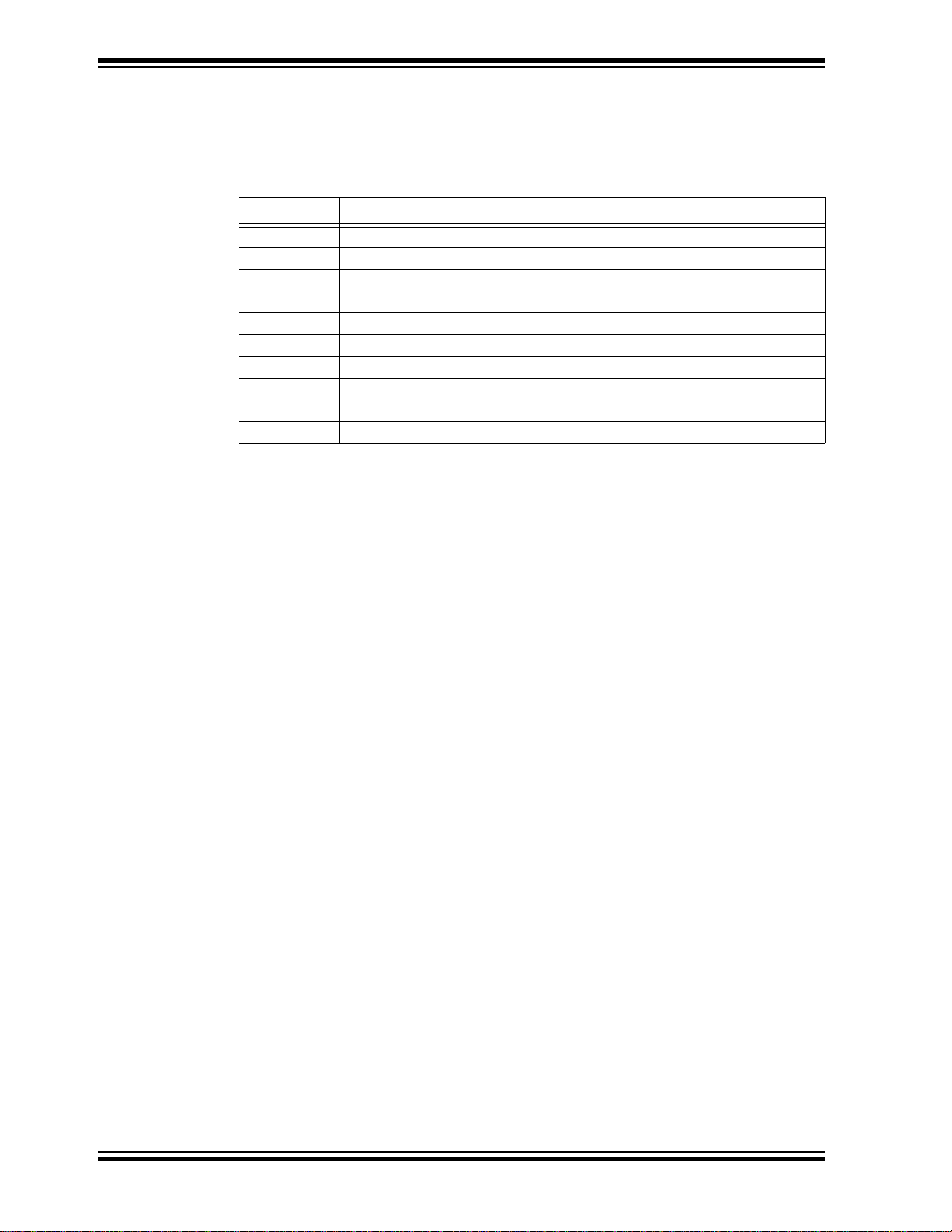
CONVENTIONS USED IN THIS GUIDE
This manual uses the following docum entat io n conven tion s:
DOCUMENTATION CONVENTIONS
Description Represents Examples
Arial font:
Italic chara c ters Referenced books MPLAB
Initial caps A window the Output window
Quotes A field name in a window or
Underlined, Italic text with
right angle bracket
Bold characters A dialog button Click OK
N‘Rnnnn A number in verilog format,
Text in angle brackets < > A key on the keyboard Press <Enter>, <F1>
Courier New font:
Plain Courier New Sample source code #define START
Italic Courier New A variable argument file.o, where file can be
Square brackets [ ] Optional arguments mcc18 [options] file
Curly brackets and pipe
character: { | }
Ellipses... Replaces r epeated text var_name [,
Preface
®
IDE User’s Guide
Emphasized text ...is the only compiler...
A dialog the Settings dialog
A menu selection select Enable Programmer
“Save project before build”
dialog
A menu path File>Save
A tab Click the Power tab
4‘b0010, 2‘hF1
where N is the tota l number of
digits, R is th e radi x and n is a
digit.
Filenames autoexec.bat
File paths c:\mcc18\h
Keywords _asm, _endasm, static
Command-line options -Opa+, -Opa-
Bit values 0, 1
Constants 0xFF, ‘A’
any valid filename
[options]
Choice of mut ually exclus ive
arguments; an OR selection
Represents code supplied by
user
errorlevel {0|1}
var_name...]
void main (void)
{ ...
}
2017 Microchip Technology Inc. DS50002569A-page 8
Page 9

RECOMMENDED READING
This user's guide descr ibes how to use 10-Pin MSOP and 8-Pin MSOP Evaluatio n
Board. The following Microchip documents are available and recommended as
supplemental reference resources:
• MCP48FEB22-E/UN Data Sheet - “8-/10-/12-Bit Single/Dual Voltage Output
Nonvolatile Digital-to-Analog Converters with SPI Interface” (DS20005429)
• MCP41x1 Data Sheet - “7/8-Bit Single/Dual SPI Digital POT with Non-Volatile
Memory” (DS22059)
• PIC12F1572 Data Sheet – “8-Pin MCU with High-Precision 16-Bit PWMs”
(DS40001723)
THE MICROCHIP WEB SITE
Microchip provides on line support via our web s ite at www.microchip.com. This web
site is used as a means to m ake files and infor mation easily availabl e to customers.
Accessible by using your favo rite In ternet bro wser, the web site contains the follow in g
information:
• Product Support – Data sheets and errata, application notes and sample
programs, design resources, user’s guides and hardware support documents,
latest software releases and archived software
• General Technical Support – Frequently Asked Questions (FAQs), technical
support requests, online discussion groups, Microchip consultant program
member listing
• Business of Microchip – Product selector and ordering guides, latest Microchip
press releases, listing of seminars and events, listings of Microchip sales offices,
distributors and factory representatives.
Preface
CUSTOMER SUPPORT
Users of Microchip products can receive assistance through several channels:
• Distributor or Representative
• Local Sales Office
• Field Application Engineer (FAE)
• Technical Support
Customers should contact th eir di str ibutor, representative or field application engineer
(FAE) for support. Local sales office s are al s o av ail ab le to help customers. A list ing of
sales offices and locations is included in the back of this document.
Technical support is available through the web site at:
http://www.microchip.com/support.
REVISION HISTORY
Revision A (April 2017)
• Original Release of this Document.
2017 Microchip Technology Inc. DS50002569A-page 9
Page 10

NOTES:
Preface
2017 Microchip Technology Inc. DS50002569A-page 10
Page 11

10-PIN MSOP AND 8-PIN MSOP
EVALUATION BOARD
USER’S GUIDE
Chapter 1. Product Overview
1.1 INTRODUCTION
This chapter provides an overview of the 10-Pin MSOP and 8-Pin MSOP Evaluation
Board and covers the following topics:
• What is the 10-Pin MSOP and 8-Pin MSOP Evaluation Board?
• 10-Pin MSOP and 8-Pin MSOP Evaluation Board Features
• What the 10-Pin MSOP and 8-Pin MSOP Evaluation Board Kit Contains
1.2 WHAT IS THE 10-PIN MSOP AND 8-PIN MSOP EVALUATION BOARD?
The 10-Pin MSOP and 8-Pin MSOP Evaluation Board (Figure 1-1) is a bond-out board
that allows the system designer to quickly evaluate the operation of Microchip
Technology’s devices in any of the following packages:
• MSOP (8- and 10-pin)
• DIP (10-pin)
Note: The 10-Pin MSOP and 8-Pin MSOP Evaluation Board can be used as an
MSOP to DIP converter.
FIGURE 1-1: 10-Pin MSOP and 8-Pin MSOP Evaluation Board Overview.
2017 Microchip Technology Inc. DS50002569A-page 11
Page 12

10-Pin MSOP and 8-Pin MSOP Evaluation Board User’s Guide
1.3 10-PIN MSOP AND 8-PIN MSOP EVALUATION BOARD FEATURES
The MSOP-10 and MSOP-8 Evaluation Board has the following features:
• Connection terminals may be either through-hole or surface-mount
• The three types of supported footprints are:
-MSOP-10
-MSOP-8
-DIP-10
• Footprints for optional passive components (SMT [0805] footprint) for:
- Power supply filtering
- Device bypass capacitor
-Filtering
- Pull-up resistor
- Pull-down resistor
- Loading resistor
- In-line resistor
- Crystal oscillator capacitors
• Silk-screen area to write specifics of implemented circuit (on back of PCB), such
as MCP48FEB2 2-E/UN.
•PICkit
• Crystal/ceramic resonator circuit footprints, SMT and THT
• Second 1 x 6 in-line connector header for interfacing to boards with PICkit Serial
Some of the Microchip family of devices that can be evaluated in the PCB include:
• Digital Potentiometers (Digi-pots)
• DAC (Digital to Analog Converters)
•PIC
• Op-amps
• Real-time clock/calendar (RTCC) chips
• Temperature sensors
• Switching regulators
TM
Serial Analyzer and/or PICkit Programming (ICSPTM) Header
Analyzer header.
®
microcontrollers
1.4 WHAT THE 10-PIN MSOP AND 8-PIN MSOP EVALUATION BOARD KIT CONTAINS?
The 10-Pin MSOP and 8-Pin MSOP Evaluation Board includes the following items:
• 10 blank Printed Circuit Boards (PCB) (ADM00309)
• Important Information Sheet
DS50002569A-page 12 2017 Microchip Technology Inc.
Page 13

Chapter 2. Installation and Operation
2.1 INTRODUCTION
This blank printed circuit board allows 8- and 10-pin devices in the following package
types to be installed: MSOP-10, MSOP-8 and DIP-10.
This board is generic so that any of the listed devices may be installed. Refer to the
device data sheet, however, for suitability of device evaluation.
As well as the device, other desired passive components (resistors and capacitors) and
connection posts may be installed. This allows the board to evaluate a minimum
configuration for the device. It also allows the device to easily be jumpered into an
existing system.
The board also has two 6-pin headers (1 x 6) whose signals can easily be jumpered to
any of the device’s pins. This allows one header to be connected for one purpose
(programming) and the other for communication to another board. An example would
be installing a PIC12F1572 (MSOP-8) in one PCB, where J1 is connected as the ICSP
(In-circuit Serial Programming) interface, and J2 in connected to be the communication
interface to the second board (PICkit Serial Analyzer interface pinout). The second
board has the MCP48FEB22-E/UN device (MSOP-10) where J1 is connected for the
PICkit Serial interface. This allows the PIC12F1572 board to be programmed to control
the MCP48FEB22-E/UN board.
10-PIN MSOP AND 8-PIN MSOP
EVALUATION BOARD
USER’S GUIDE
2017 Microchip Technology Inc. DS50002569A-page 13
Page 14
10-Pin MSOP and 8-Pin MSOP Evaluation Board User’s Guide
2.2 GETTING STARTED
The pins of the 8-pin device are tied together with the upper pins of the 10-pin device
(1-4 and 7-10); see Table 2-1.
TABLE 2-1: MSOP FOOTPRINTS PIN CORRESPONDENCE
MSOP—10 MSOP—8Comments
11
22
33
44
5—
6—
75
86
97
10 8
The pads’ indexes correspond to the MSOP-10 pin indexes. For example, pad P05 is
connected to the pin 5 of the MSOP-10 package.
The footprints for the pull-up (RUx), pull-down (RDx) and series (RSx) devices are
labeled in relation to the MSOP-10 package. For example, pin 1 is connected to RU1,
RD1 and RS1.
This circuit allows each pin to individually have any of the following: a pull-up resistor,
a pull-down resistor (or a loading/filtering capacitor) and a series resistor.
Power supply filtering capacitors are connected between the V
and C2). The circuit has two 6-pin headers that can be used for PICkit Serial communication as well as PIC ICSP, or to connect two evaluation board together. The signals
of the headers need to be jumpered to the appropriate device pins.
and VSS pads (C1
DD
DS50002569A-page 14 2017 Microchip Technology Inc.
Page 15

Installation and Operation
Figure 2-1 shows the evaluation board circuit, and an example of connecting signals
from the J1 header to the device pins with jumper wire.
FIGURE 2-1: 10-Pin MSOP and 8-Pin MSOP Evaluation Board Circuit.
2017 Microchip Technology Inc. DS50002569A-page 15
Page 16

10-Pin MSOP and 8-Pin MSOP Evaluation Board User’s Guide
2.3 HARDWARE DESCRIPTION
Figure 2-2 and Figure 2-3 show the top side and bottom side of the component layout
of the 10-Pin MSOP and 8-Pin MSOP Evaluation Board.
FIGURE 2-2: 10-Pin MSOP and 8-Pin MSOP Evaluation Board - Top View.
FIGURE 2-3: 10-Pin MSOP and 8-Pin MSOP Evaluation Board - Bottom View.
DS50002569A-page 16 2017 Microchip Technology Inc.
Page 17

Installation and Operation
The 10-Pin MSOP and 8-Pin MSOP Evaluation Board is a four-layer board
(62 mm x 48 mm). There are ten connection points/pads that can use either
through-hole or surface-mount connector posts.
The pad labeled V
is connected to the PCB ground plane. All the passive components that are connected
to V
or VSS are connected to either the power plane or ground plane. The 10 remain-
DD
ing PCB pads correspond to the device pins (e.g., pad 1 connects to pin1).
Each pad has three passive components associated with them: a pull-up resistor, a
pull-down resistor and an in line series resistor. The pull-up resistor is always RUx and
the pull-down resistor is RDx. The “X” is a numeric value that corresponds to a particular pad (1 to 8). As an example, Pad 5’s pull-up resistor is RU5. Capacitor C1 and C2
are the power supply filtering capacitors. For whichever pin is the device’s V
RDx component footprint can be used for the device’s bypass capacitor. Table 2-1
describes the components.
Two 6-pin header interfaces are available (J1 and J2). Header J1 will typically be used
for the PICkit Serial or the PIC In-Circuit Serial Programming (ICSP) interface. Header
J2 allows a custom interface for connecting to other boards (see Figure 2-17).
For additional information, refer to Section 2.4.6 “PICkit Serial or In-Circuit Serial
Programming (ICSP) Interface (Header J1)”. Figure 2-4 shows an example of a Con-
nection between two boards, one acting as a controller for the second one, which contains the device to be evaluated. Not all connections are illustrated.
is connected to the PCB power plane, while the pad labeled VSS
DD
, the
DD
FIGURE 2-4: Example of Two PCB System.
2017 Microchip Technology Inc. DS50002569A-page 17
Page 18

10-Pin MSOP and 8-Pin MSOP Evaluation Board User’s Guide
The optional components of the 10-Pin MSOP and 8-Pin MSOP Evaluation Board are
displayed in Table 2-2.
TABLE 2-2: OPTIONAL COMPONENTS
Component Comment
C1, C2 Power supply bypass capacit ors
C3, C4 Crystal capacitors
RU1, RU3, RU3, RU4, RU5, RU6,
RU7, RU8, RU9, RU10
RD1, RD2, RD2, RD3, RD4, RD5,
RD6, RD7, RD8, RD9, RD10
RS1, RS2, RS3, RS4, RS5, RS6,
RS7, RS8, RS9, RS10
R1 Used in case of devi ces that have multiplexed SDI/SDO
Y1 Used to generate a clock signal
J1 PICkit Serial/ICSP header
J2
Note 1: Whichever pin is the device’s VDD pin, that corresponding RDx footprint
can be used for the device’s bypass capacitor. Example: If pin 8 is the
device’s V
pin, then install the bypass capacitor in the RD8 footprint.
DD
2: All passive components use the surface mount [0805] footprint.
Pull-up resistors
Pull-down resistors
Series resistors. When using a PIC MCU, placing a
resistor in the RSx and a capacitor in the RDx locations
creates a low-pass filter which can be used to generate a
variable output voltage if connected to a PWM-capable
pin.
pins, for example the MCP45x1
Generic 6-pin header, used to connect two evaluation
boards together
DS50002569A-page 18 2017 Microchip Technology Inc.
Page 19

Installation and Operation
2.4 10-PIN MSOP AND 8-PIN MSOP EVALUATION BOARD DESCRIPTION
This section describes the working principles and limitations that should be taken into
account when using the10-Pin MSOP and 8-Pin MSOP Evaluation Board.
2.4.1 Power and Ground
The10-Pin MSOP and 8-Pin MSOP Evaluation Board has a VDD pad and a VSS pad.
These pads can have connection posts installed that allows easy connection to the
power (V
surface-mount connectors.
The power and ground planes are connected to the appropriate passive components
on the PCB (such as power plane to RUx and ground plane to RDx components).
2.4.2 PCB Pads
For each package pin (pins 1 to 10), there is a PCB pad (pads 1 to 10). The device has
power pins (V
power and ground plane have been installed close to each PCB pad. This allows any
pad to be connected to the power or ground plane, so when power is connected to the
V
and VSS pads, it is also connected to the appropriate device pin (see Figure 2-5).
DD
) and ground (VSS) planes. The layout allows either through-hole or
DD
) and ground pins (VSS). To ease connections on the PCB, vias to the
DD
FIGURE 2-5: Connecting the PCB Pad to Either the VDD or VSS Pins.
The series components (RSx) can be used in conjunction with the RDx components to
create passive filters. For example, when using a PIC microcontroller, one could generate an analog signal by low pass-filtering the PWM signal coming from a digital output
pin. In order to use the RSx footprint, the PCB trace passing through the middle of the
footprint should be cut using a sharp tool.
2017 Microchip Technology Inc. DS50002569A-page 19
Page 20

10-Pin MSOP and 8-Pin MSOP Evaluation Board User’s Guide
See Figure 2-6 to observe how to create an RC output filter by cutting the trace
between the two Pads for component RS6 and then installing the desired resistor at
that location. The capacitor is then installed at component RD6.
FIGURE 2-6: Creating an RC output filter
2.4.3 Passive Components - RUx, RDx, RSx, C1 and C2
The footprints for these components allow maximum flexibility in the use of this PCB to
evaluate a wide range of devices. The purpose of these components may vary depending on the device under evaluation and how it is to be used in the desired circuit. Refer
to the device data sheet for the recommended components that should be used when
evaluating that device.
• Component RUx allows a pull-up resistor to be installed for the device pin.
• Component RDx allows a pull-down resistor or a a capacitive load/filter to be
installed for the device pin.
• Component RSx allows a series component to be fitted.
• Component C1 and C2 allows power supply filtering capacitors to be installed.
2.4.4 Multiplexing Resistor R1
Due to the number of pins available in a specific package, some digital potentiometers
multiplex together the SDI and SDO signals. It is therefore necessary to connect the
two signal lines coming from the host to a single pin on the device. The digital potentiometer needs a way to overdrive the host controller’s SDO signal.
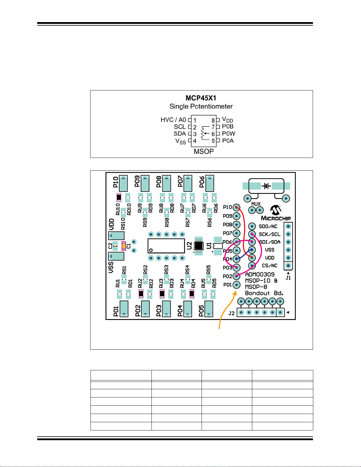
Figure 2-7 shows an example connection, from the MCP45x1 data sheet. The R1 value
would need to be determined based on the V
devices.
FIGURE 2-7: Multiplexed SDI/SDO Connection Example.
, VOH and VOL levels of the two
IH,VIL
DS50002569A-page 20 2017 Microchip Technology Inc.
Page 21

Installation and Operation
2.4.5 Device Footprints
This section describes the characteristics of the component footprints so that you are
better able to determine if the desired component(s) are compatible with the board.
2.4.5.1 MSOP-10
The 10-pin MSOP footprint has been laid out for packages that have a typical pitch of
0.50 BSC, a maximum lead width of 0.41 mm, and a maximum molded package width
of 3 BSC. T en-lead (or less) MSOP packages that meet these characteristics should be
able to be used with this board.
2.4.5.2 MSOP-8
The 8-pin MSOP footprint has been laid out for packages that have a typical pitch of
0.65 mm (BSC), a maximum lead width of 0.4mm, and a maximum molded package
width of 3 mm BSC. Eight-lead MSOP packages that meet these characteristics should
be able to be used with this board.
2.4.5.3 DIP-10
The 10-pin DIP footprint has been laid out for packages that have a typical pitch of
100 mil (BSC), a maximum lead width of 22 mil and a molded package width of 600 mil.
2.4.5.4 PASSIVE COMPONENTS
All passive components (R1, RUx, RDx, RSx and Cx) use a surface mount [0805] foot-
print. Any component that has a compatible footprint can be used with this board.
2.4.5.5 HEADERS (1 X 6)
The headers have a typical pitch of 100 mil (BSC). The headers are designed to be
compatible with the PICkit Serial Analyzer and PICkit 3 Programmer.
2017 Microchip Technology Inc. DS50002569A-page 21
Page 22

10-Pin MSOP and 8-Pin MSOP Evaluation Board User’s Guide
Connected to Ground Plane
Connected to Power Plane
TOP BOTTOM
2.4.6 PICkit Serial or In-Circuit Serial Programming (ICSP) Interface
(Header J1)
Figure 2-8 shows the interface connection of the J1 Header. The VDD and VSS signals
are connected to the appropriate power or ground plane. The other four signals are
open and can be easily jumpered to any of the 10 P1 through P10 connection points.
The top layer silk screen indicates the common PICkit Serial signal names, while the
bottom layer silk screen indicate s the ICSP sig nal names .
FIGURE 2-8: PICkit Serial / ICSP Interface Connections.
2.4.6.1 PICKIT SERIAL INTERFACE
Table 2-3 shows the pin number assignment for the different signals for each of the
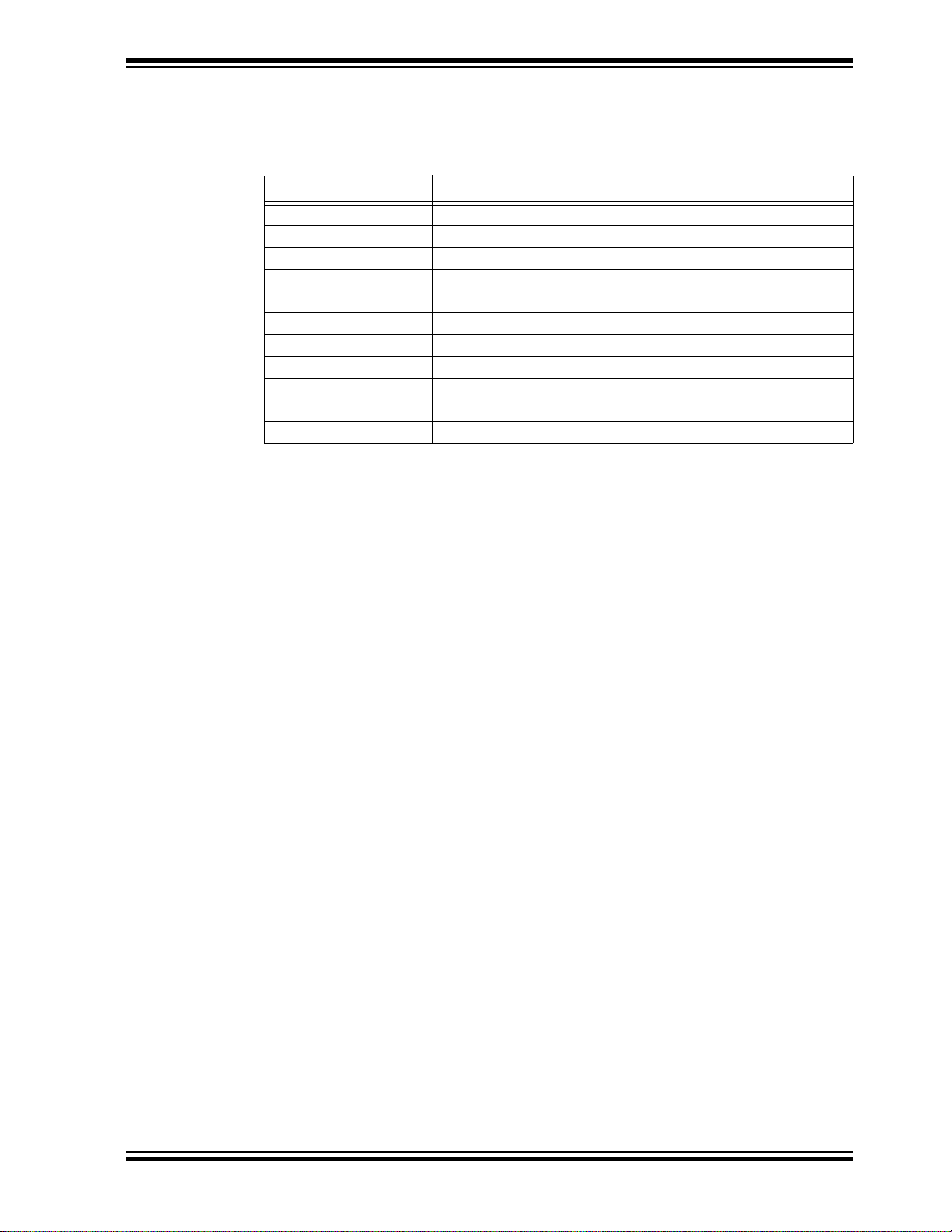
supported interface protocols (SPI, I
TABLE 2-3: PICKIT SERIAL HEADER SIGNALS
Pin
Number
1 CS — TX CS TX
2V
3V
4 SDI SDA — SDI CS/WAKE
5 SCK SCL — SCK FAULT/TXE
6 SDO — RX SDO RX
SPI I
DD
SS
2
C USART Microwire LIN
V
DD
V
SS
2
C, and others).
PICkit Serial Header Signal
V
DD
V
SS
V
DD
V
SS
—
V
SS
DS50002569A-page 22 2017 Microchip Technology Inc.
Page 23

Installation and Operation
2.4.6.2 ICSP INTERFACE
The ICSP interface al low s a PI C MCU device t o be pro gr ammed w ith programmers that
support this interface , such as the PICkit 3 p r ogramme r (Part Num b er: PG16413 0).
Table 2-4 shows the pin number assignment for the ICSP signa ls.
TABLE 2-4: ICSP HEADER SIGNALS
Pin
Number
1 VPP High Voltage Signal
2VDD—
3 VSS —
4 PCD ICSP™ Data
5 PCC ICSP™ Clock
6——
2.4.7 Board interconnect header (Header J2)
Figure 2-9 shows the interface connection of J2 Header. This header allows two
ADM00309 boards to be inter-connected, which permits a microcontroller from one of
the boards to be used as a controller for the device on the second board. The six
connector signals are routed out to six holes, which should be wired to the appropriate
pins.
ICSP Signal Comments
FIGURE 2-9: J2 Header Connections.
2017 Microchip Technology Inc. DS50002569A-page 23
Page 24

10-Pin MSOP and 8-Pin MSOP Evaluation Board User’s Guide
48FEB
Required “Jumpers” for PICkit Serial operation.
Note: VDD, VSS are connected to
appropriate power plane.
2.5 EVALUATING THE MCP48FEBXX DIGITAL-TO-ANALOG CONVERTERS
The MCP48FEBXX are single and dual-channel, 8-bit, 10-bit, and 12-bit, buffered
voltage output Digital-to-Analog Converters (DAC) with nonvolatile memory and an
SPI serial interface.
The DAC reference voltage can be selected as the VREF pin, the device V
internal band gap voltage. When V
DAC refe rence circuit. When the V
selected to be 1x or 2x. When the gain is 2x, the V
a maximum of V
DD/2
.
is selected, VDD is connected internally to the
DD
pin is used, the output buffer’s gain to can be
REF
pin voltage should be limited to
REF
Figure 2-10 shows the pinouts of the MCP48FEBXX family.
DD
or the
FIGURE 2-10: MCP48FEBXX Family Pinout.
Figure 2-11 represents PICkit Serial/ICSP Header and Example Connections for
MCP48FEBXX.
0
C
0
FIGURE 2-11: MCP48FEBXX PICkit Serial Header Example Connections.
DS50002569A-page 24 2017 Microchip Technology Inc.
Page 25

Installation and Operation
Table 2-5 shows other DACs that are compatible with this evaluation board.
TABLE 2-5: SUPPORTED DIGITAL-TO ANALOG CONVERTERS
Device MSOP-8 MSOP-10 Comments
MCP4801 Y—
MCP4802 Y—
MCP48FEB01 —Y
MCP48FEB02 —Y
MCP48FVB01 —Y
MCP48FVB02 —Y
MCP4901 Y—
TC1320 Y—
MCP4811 Y—
MCP4812 Y—
MCP48FEB11 —Y
MCP48FEB12 —Y
MCP48FVB11 —Y
MCP48FVB12 —Y
MCP4911 Y—
TC1321 Y-—
MCP4728 —Y
MCP4821 Y—
MCP4822 Y—
MCP48FEB21 —Y
MCP48FEB22 —Y
MCP48FVB21 —Y
MCP48FVB22 —Y
MCP4921 Y—
2017 Microchip Technology Inc. DS50002569A-page 25
Page 26
10-Pin MSOP and 8-Pin MSOP Evaluation Board User’s Guide
Required “Jumpers” for PICkit Serial operation.
Note: VDD, VSS are connected to
appropriate power plane.
2.6 EVALUATING THE 45X1 DIGITAL POTENTIOMETERS
The MCP45x1 is a family of digital potentiometers that offers 7- and 8-bit resistor networks as well as volatile and non-volatile memories options, in a MSOP 8-pin package.The MCP45X1 8-pin package is shown in Figure 2-12. The family works with an
2
I
C serial interface with speeds of 100 kHz, 400 kHz and 3.4 MHz. The PICkit Serial
Analyzer can be used to communicate with the devices. The proper connections are
being shown in Figure 2-13. Other Digital Potentiometers that are supported by this
evaluation board are shown in Table 2-6.
FIGURE 2-12: MCP45x1 Family Pinout.
0
C
R
R
45X1
0
FIGURE 2-13: MCP45x1 PICkit Serial Header Example Connections.
TABLE 2-6: SUPPORTED DIGITAL POTENTIOMETER FAMILIES
Device MSOP-8 MSOP-10 Comments
MCP413x Y—
MCP41x2 Y—
MCP42x2 —Y
MCP45x1 Y—
MCP45x2 Y—
MCP46x2 —Y
DS50002569A-page 26 2017 Microchip Technology Inc.
Page 27

Installation and Operation
2.6.1 Evaluating the PIC12F1572 Device (XLP PIC Microcontroller)
The PIC12F1572 is a nanowatt XLP PIC Microcontroller that is offered in an 8-lead
MSOP package. This device can be installed on the top side of the PCB. Figure 2-14
shows the PIC12F1572’s pin out, while Figure 2-15 shows an example connection for
the ICSP interface and the connection of the crystal circuit to the secondary oscillator.
FIGURE 2-14: PIC12F1572 Pinout.
2017 Microchip Technology Inc. DS50002569A-page 27
Page 28

10-Pin MSOP and 8-Pin MSOP Evaluation Board User’s Guide
FIGURE 2-15: PIC12F1572 ICP Header Example Connections Bottom View.
FIGURE 2-16: PIC12F1572 ICP Header Example Connections Top View.
DS50002569A-page 28 2017 Microchip Technology Inc.
Page 29
Installation and Operation
Other nanowatt XLP PIC Microcontrollers that are supported by this evaluation board
are shown in Table 2-7.
TABLE 2-7: SUPPORTED MSOP-8 PIC MICROCONTROLLERS
Device Family/Core Comments
PIC12F508 Baseline 8-bit
PIC12F509 Baseli ne 8-bi t
PIC12F510 Baseline 8-bit
PIC12F609 Mid-Range 8-bit
PIC12F615 Mid-Range 8-bit
PIC12F1501 Enhanced Mid-Range
PIC12F1571 Enhanced Mid-Range
PIC12F1572 Enhanced Mid-Range
PIC12F617 Mid-Range 8-bit
PIC12F519 Baseli ne 8-bi t
PIC12LF1552 Mid-Range 8-bit
2017 Microchip Technology Inc. DS50002569A-page 29
Page 30

10-Pin MSOP and 8-Pin MSOP Evaluation Board User’s Guide
PIC
DAC
Appropriate headers fitted
0
0
0
0
0
R
PicKIT3
(typically the PICkit Serial
Analyser pinout)
2.7 CREATING A SYSTEM WITH A PIC12F1572 MICROCONTROLLER AND A MCP48FEB22 DAC
The following image illustrates how to connect two ADM00309 boards in order to obtain
a functional system. One board hosts a PIC12Fxxxx, which is programmed using a
PicKIT3 connected to J1, and controls a second board, which has a
MCP48FEB22-E/UN device installed. The J2 connector of the PIC board is used as a
serial communication port, being connected to J1 of the DAC board.
FIGURE 2-17: Creating a Two-Board Evaluation System.
DS50002569A-page 30 2017 Microchip Technology Inc.
Page 31

NOTES:
Installation and Operation
2017 Microchip Technology Inc. DS50002569A-page 31
Page 32

10-Pin MSOP and 8-Pin MSOP Evaluation Board User’s Guide
DS50002569A-page 32 2017 Microchip Technology Inc.
Page 33

Appendix A. Schematic and Layouts
Top Layer
Ground Layer
Power Layer
Bottom Layer
A.1 INTRODUCTION
This appendix contains the following schematics and layouts for the 10-Pin MSOP and
8-Pin MSOP Evaluation Board:
• Board – Schematic
• Board – Top Silk Layer
• Board – Top Copper and Silk Layer
• Board – Top Copper
• Board – Bottom Copper Layer
• Board – Bottom Copper and Silk Layer
A.2 SCHEMATICS AND PCB LAYOUT
Section A.3 “Board – Schematic” shows the schematic of the 10-Pin MSOP and
8-Pin MSOP Evaluation Board.
Section A.4 “Board – Top Silk Layer” shows the layout for the top layer of the 10-Pin
MSOP and 8-Pin MSOP Evaluation Board. The layer order is shown in Figure A-1.
10-PIN MSOP AND 8-PIN MSOP
EVALUATION BOARD
USER’S GUIDE
FIGURE A-1: Layer Order.
2017 Microchip Technology Inc. DS50002569A-page 33
Page 34

10-Pin MSOP and 8-Pin MSOP Evaluation Board
SDO/NC/LVP
SCK/SCL/PGC
SDI/SDA/PGD
VSS
VDD
CS/NC/VPP
X1
X2
PX2PX1
R1
TP9
SDO
SCK
SDI
VSS
VDD
CSS
TP10
TP11
TP12
TP13
TP14
TP26
TP25
RS1 P01
1 1
VDD
PAD01
PV31PV4
VDDVSS
PV2
1
PV1
1
2
3
4
5 6
7
8
9
10
U1
MSOP-10
1
2
3
4 5
6
7
8
U2
MSOP-8
PD01
PD02
PD03
PD04
PD05
PD10
PD09
PD08
PD07
PD06
PAD01
PAD02
PAD03
PAD04
PAD05 PAD06
PAD07
PAD08
PAD09
PAD10
12345
DIP10_A
J11
12345
DIP10_B
J12
RU1
RD1
VSS
RS2 P02
1 1
VDD
PAD02
RU2
RD2
VSS
RS3 P03
1 1
VDD
PAD03
RU3
RD3
VSS
RS4 P04
1 1
VDD
PAD04
RU4
RD4
VSS
RS5 P05
1 1
VDD
PAD05
RU5
RD5
VSS
RS10P10
1 1
VDD
PAD10
RU10
RD10
VSS
RS9P09
1 1
VDD
PAD09
RU9
RD9
VSS
RS8P08
1 1
VDD
PAD08
RU8
RD8
VSS
RS7P07
1 1
VDD
PAD07
RU7
RD7
VSS
RS6P06
1 1
VDD
PAD06
RU6
RD6
VSS
TP3
TP4
TP5
TP6
TP7
TP8
1
2
3
4
5
6
B2B Connector
J2
VSS
VSS
0805
C1
0805
C2
0805
C4
0805
C3
1
2
3
4
5
6
PKSA
J1
A.3 BOARD – SCHEMATIC
DS50002569A-page 34 2017 Microchip Technology Inc.
Page 35

A.4 BOARD – TOP SI LK LAYER
Schematic and Layouts
2017 Microchip Technology Inc. DS50002569A-page 35
Page 36

10-Pin MSOP and 8-Pin MSOP Evaluation Board
A.5 BOARD – TOP COPPER AND SILK LAY ER
DS50002569A-page 36 2017 Microchip Technology Inc.
Page 37

A.6 BOARD – TOP COPPER
Schematic and Layouts
2017 Microchip Technology Inc. DS50002569A-page 37
Page 38

10-Pin MSOP and 8-Pin MSOP Evaluation Board
A.7 BOARD – BOTTOM COPPER LAYER
DS50002569A-page 38 2017 Microchip Technology Inc.
Page 39

A.8 BOARD – BOTTOM COPPER AND SILK LAYER
Schematic and Layouts
2017 Microchip Technology Inc. DS50002569A-page 39
Page 40

10-Pin MSOP and 8-Pin MSOP Evaluation Board
A.9 BOARD – BOTTOM SILK LAYER
DS50002569A-page 40 2017 Microchip Technology Inc.
Page 41

Worldwide Sales and Service
AMERICAS
Corporate Office
2355 West Chandler Blvd.
Chandler, AZ 85224-6199
Tel: 480-792-7200
Fax: 480-792-7277
Technica l Support:
http://www.microchip.com/
support
Web Address:
www.microchip.com
Atlanta
Duluth, GA
Tel: 678-957-9614
Fax: 678-957-1455
Austin, TX
Tel: 512-257-3370
Boston
Westborough, MA
Tel: 774-760-0087
Fax: 774-760-0088
Chicago
Itasca, IL
Tel: 630-285-0071
Fax: 630-285-0075
Dallas
Addison, TX
Tel: 972-818-7423
Fax: 972-818-2924
Detroit
Novi, MI
Tel: 248-848-4000
Houston, TX
Tel: 281-894-5983
Indianapolis
Noblesville, IN
Tel: 317-773-8323
Fax: 317-773-5453
Tel: 317-536-2380
Los Angeles
Mission Viejo, CA
Tel: 949-462-9523
Fax: 949-462-9608
Tel: 951-273-7800
Raleigh, NC
Tel: 919-844-7510
New Yor k , NY
Tel: 631-435-6000
San Jose, CA
Tel: 408-735-9110
Tel: 408-436-4270
Canada - Toronto
Tel: 905-695-1980
Fax: 905-695-2078
ASIA/PACIFIC
Asia Pacific Office
Suites 3707-14, 37th Floor
Tower 6, The Gateway
Harbour City, Kowloon
Hong Kong
Tel: 852-2943-5100
Fax: 852-2401-3431
Australia - Sydney
Tel: 61-2-9868-67 33
Fax: 61-2-9868-6755
China - Beijing
Tel: 86-10-8569-7 000
Fax: 86-10-8528-2104
China - Chengdu
Tel: 86-28-8665-5 511
Fax: 86-28-8665-7889
China - Chongqing
Tel: 86-23-8980-9 588
Fax: 86-23-8980-9500
China - Dongguan
Tel: 86-769-8702-9880
China - Guangzhou
Tel: 86-20-8755-8 029
China - Hangzhou
Tel: 86-571-8792-8115
Fax: 86-571-8792-8116
China - Hong Kong SAR
Tel: 852-2943-5100
Fax: 852-2401-3431
China - Nanjing
Tel: 86-25-8473-2 460
Fax: 86-25-8473-2470
China - Qingdao
Tel: 86-532-8502-7355
Fax: 86-532-8502-7205
China - Shanghai
Tel: 86-21-3326-8 000
Fax: 86-21-3326-8021
China - Shenyang
Tel: 86-24-2334-2 829
Fax: 86-24-2334-2393
China - Shenzhen
Tel: 86-755-8864-2200
Fax: 86-755-8203-1760
China - Wuhan
Tel: 86-27-5980-5 300
Fax: 86-27-5980-5118
China - Xian
Tel: 86-29-8833-7 252
Fax: 86-29-8833-7256
ASIA/PACIFIC
China - Xiamen
Tel: 86-592-2388138
Fax: 86-592-2388130
China - Zhuhai
Tel: 86-756-3210040
Fax: 86-756-3210049
India - Bangalore
Tel: 91-80-3090-4444
Fax: 91-80-3090-4123
India - New Delhi
Tel: 91-11-4160-8631
Fax: 91-11-4160-8632
India - Pune
Tel: 91-20-3019-1500
Japan - Osaka
Tel: 81-6-6152-7160
Fax: 81-6-6152-9310
Japan - Tokyo
Tel: 81-3-6880- 3770
Fax: 81-3-6880-3771
Korea - Daegu
Tel: 82-53-744-4301
Fax: 82-53-744-4302
Korea - Seoul
Tel: 82-2-554-7200
Fax: 82-2-558-5932 or
82-2-558-5934
Malaysia - Kuala Lumpur
Tel: 60-3-6201-9857
Fax: 60-3-6201-9859
Malaysia - Penang
Tel: 60-4-227-8870
Fax: 60-4-227-4068
Philippines - Manila
Tel: 63-2-634-9065
Fax: 63-2-634-9069
Singapore
Tel: 65-6334-8870
Fax: 65-6334-8850
Tai wan - Hsin Chu
Tel: 886-3-5778-366
Fax: 886-3-5770-955
Taiwan - Kaohsiung
Tel: 886-7-213-7830
Taiwan - Taipei
Tel: 886-2-2508-8600
Fax: 886-2-2508-0102
Thailand - Bangkok
Tel: 66-2-694-1351
Fax: 66-2-694-1350
EUROPE
Austria - Wels
Tel: 43-7242-2244-39
Fax: 43-7242-2244-393
Denmark - Copenhagen
Tel: 45-4450-2828
Fax: 45-4485-2829
Finland - Esp oo
Tel: 358-9-4520-820
France - Paris
Tel: 33-1-69-53 -63-20
Fax: 33-1-69-30-90-79
France - Saint Cloud
Tel: 33-1-30-60 -70-00
Germany - Garching
Tel: 49-8931-9700
Germany - Haan
Tel: 49-2129-3766400
Germany - Heilbronn
Tel: 49-7131-67-3636
Germany - Karlsruhe
Tel: 49-721-625370
Germany - Munich
Tel: 49-89-627-144-0
Fax: 49-89-627-144-44
Germany - Rosenheim
Tel: 49-8031-354-560
Israel - Ra’anana
Tel: 972-9-744-7705
Italy - Milan
Tel: 39-0331-742611
Fax: 39-0331-466781
Italy - Padova
Tel: 39-049-7625286
Netherlands - Drunen
Tel: 31-416-690399
Fax: 31-416-690340
Norway - Trondheim
Tel: 47-7289-7561
Poland - Wars a w
Tel: 48-22-3325737
Romania - Bucharest
Tel: 40-21-407-87-50
Spain - Madrid
Tel: 34-91-708-08-90
Fax: 34-91-708-08-91
Sweden - Gothenberg
Tel: 46-31-704-60-40
Sweden - Stockholm
Tel: 46-8-5090-4654
UK - Wokingham
Tel: 44-118-921-5800
Fax: 44-118-921-5820
DS50002569A-page 41 2016 Microchip Technology Inc.
11/07/16
 Loading...