

Page 1

USB7252
4-Port USB 3.2 Gen 2 Type-C® Controller Hub
Highlights
• 4-Port USB Smart Hub with:
- USB Gen 2 Type-B® on upstream port
- Native USB Gen 2 Type-C with Power Delivery PD
support on downstream ports 1 and 2
- One Standard USB 3.2 Gen 2 downstream port
- One Standard USB 2.0 downstream port
®
- Internal Hub Feature Controller enables:
- USB to I2C/SPI/UART/I2S/GPIO bridge endpointsupport
- USB to internal hub register write and read
• USB Link Power Management (LPM) support
• Programming of firmware image to external SPI
memory device from USB host
• USB-IF Battery Charger revision 1.2 support on
downstream ports (DCP, CDP, SDP)
• Enhanced OEM configuration options available
through either OTP or external SPI memory
• Available in 100-pin (12mm x 12mm) VQFN
RoHS compliant package
• Commercial and industrial grade temperature
support
Target Applications
• Standalone USB Hubs
• Laptop Docks
• PC Motherboards
• PC Monitor Docks
• Multi-function USB 3.2 Gen 2 Peripherals
Key Benefits
• USB 3.2 Gen 2 compliant 10 Gbps, 5 Gbps,
480 Mbps, 12 Mbps, and 1.5Mbps operation
- 5V tolerant USB 2.0 pins
- 1.21V tolerant USB 3.2 Gen 2 pins
- Integrated termination and pull-up/down resistors
• Native USB Type-C Support
- Type-C CC Pin with integrated Rp and Rd resistors
- Integrated multiplexer on USB Type-C enabled
ports. USB 3.2 Gen 2 PHYs are disabled until a
valid Type-C attach is detected, saving idle power.
Control for external VCONN supply
* USB Type-C® and USB-C® are registered trademarks of USB Implementers Forum
• Supports battery charging of most popular battery
powered devices on all ports
- USB-IF Battery Charging rev. 1.2 support
(DCP, CDP, SDP)
®
- Apple
- Chinese YD/T 1591-2006/2009 charger emulation
- European Union universal mobile charger support
- Supports additional portable devices
portable product charger emulation
• On-chip Microcontroller
- manages I/Os, VBUS, and other signals
• 96kB RAM, 256kB ROM
• 8kB One-Time-Programmable (OTP) ROM
- Includes on-chip charge pump
• Configuration programming via OTP Memory, SPI
external memory, or SMBus
• FlexConnect
- The roles of the upstream and all downstream
ports are reversible on command
• Multi-Host Endpoint Reflector
- Integrated host-controller endpoint reflector via
CDC/NCM device class for automotive applications
• USB Bridging
- USB to I2C, SPI, UART, I2S, and GPIO
• PortSwap
- Configurable USB 2.0 differential pair signal swap
• PHYBoost
- Programmable USB transceiver drive strength for
recovering signal integrity
• VariSense
- Programmable USB receive sensitivity
• PortSplit
- USB 2.0 and USB 3.2 Gen 2 port operation can be
split for custom applications using embedded USB
3.x devices in parallel with USB 2.0 devices
• Compatible with Microsoft Windows 10, 8, 7, XP,
Apple OS X 10.4+, and Linux hub drivers
• Optimized for low-power operation and low thermal dissipation
• 100-pin VQFN package (12mm x 12mm)
2018 - 2020 Microchip Technology Inc. DS00002736D-page 1
Page 2

USB7252
TO OUR VALUED CUSTOMERS
It is our intention to provide our valued customers with the best documentation possible to ensure successful use of
your Microchip products. To this end, we will continue to improve our publications to better suit your needs. Our publications will be refined and enhanced as new volumes and updates are introduced.
If you have any questions or comments regarding this publication, please contact the Marketing Communications
Department via E-mail at docerrors@microchip.com or fax the Reader Response Form in the back of this data
sheet to (480) 792-4150. We welcome your feedback.
Most Current Data Sheet
To obtain the most up-to-date version of this data sheet, please register at our Worldwide Web site at:
http://www.microchip.com
You can determine the version of a data sheet by examining its literature number found on the bottom outside corner
of any page. The last character of the literature number is the version number, (e.g., DS30000A is version A of document DS30000).
Errata
An errata sheet, describing minor operational differences from the data sheet and recommended workarounds, may
exist for current devices. As device/documentation issues become known to us, we will publish an errata sheet. The
errata will specify the revision of silicon and revision of document to which it applies.
To determine if an errata sheet exists for a particular device, please check with one of the following:
• Microchip’s Worldwide Web site; http://www.microchip.com
• Your local Microchip sales office (see last page)
When contacting a sales office, please specify which device, revision of silicon and data sheet (include literature number) you are using.
Customer Notification System
Register on our web site at www.microchip.com to receive the most current information on all of our products.
DS00002736D-page 2 2018 - 2020 Microchip Technology Inc.
Page 3

USB7252
1.0 PREFACE
1.1 General Terms
TABLE 1-1: GENERAL TERMS
Term Description
ADC Analog-to-Digital Converter
Byte 8 bits
CDC Communication Device Class
CSR Control and Status Registers
DFP Downstream Facing Port
DWORD 32 bits
EOP End of Packet
EP Endpoint
FIFO First In First Out buffer
FS Full-Speed
FSM Finite State Machine
GPIO General Purpose I/O
HS Hi-Speed
HSOS High Speed Over Sampling
Hub Feature Controller The Hub Feature Controller, sometimes called a Hub Controller for short is the internal
processor used to enable the unique features of the USB Controller Hub. This is not to
be confused with the USB Hub Controller that is used to communicate the hub status
back to the Host during a USB session.
2
C Inter-Integrated Circuit
I
LS Low-Speed
lsb Least Significant Bit
LSB Least Significant Byte
msb Most Significant Bit
MSB Most Significant Byte
N/A Not Applicable
NC No Connect
OTP One Time Programmable
PCB Printed Circuit Board
PCS Physical Coding Sublayer
PHY Physical Layer
PLL Phase Lock Loop
RESERVED Refers to a reserved bit field or address. Unless otherwise noted, reserved bits must
always be zero for write operations. Unless otherwise noted, values are not guaranteed when reading reserved bits. Unless otherwise noted, do not read or write to
reserved addresses.
SDK Software Development Kit
SMBus System Management Bus
UFP Upstream Facing Port
UUID Universally Unique IDentifier
WORD 16 bits
2018 - 2020 Microchip Technology Inc. DS00002736D-page 3
Page 4

USB7252
1.2 Buffer Types
TABLE 1-2: BUFFER TYPES
Buffer Type Description
I Input.
IS Input with Schmitt trigger.
O12 Output buffer with 12 mA sink and 12 mA source.
OD12 Open-drain output with 12 mA sink
PU 50 μA (typical) internal pull-up. Unless otherwise noted in the pin description, internal pull-
PD 50 μA (typical) internal pull-down. Unless otherwise noted in the pin description, internal
ICLK Crystal oscillator input pin
OCLK Crystal oscillator output pin
I/O-U Analog input/output defined in USB specification.
I-R RBIAS.
A Analog.
AIO Analog bidirectional.
P Power pin.
ups are always enabled.
Internal pull-up resistors prevent unconnected inputs from floating. Do not rely on internal
resistors to drive signals external to the device. When connected to a load that must be
pulled high, an external resistor must be added.
pull-downs are always enabled.
Internal pull-down resistors prevent unconnected inputs from floating. Do not rely on
internal resistors to drive signals external to the device. When connected to a load that
must be pulled low, an external resistor must be added.
DS00002736D-page 4 2018 - 2020 Microchip Technology Inc.
Page 5
USB7252
1.3 Pin Reset States
The pin reset state definitions are detailed in Table 1-3. Refer to Section 3.1, Pin Assignments for details on individual
pin reset states.
TABLE 1-3: PIN RESET STATE LEGEND
Symbol Description
AI Analog input
AIO Analog input/output
AO Analog output
PD Hardware enables pull-down
PU Hardware enables pull-up
Y Hardware enables function
Z Hardware disables output driver (high impedance)
PU Hardware enables internal pull-up
PD Hardware enables internal pull-down
1.4 Reference Documents
1. Universal Serial Bus Revision 3.2 Specification, http://www.usb.org
2. Battery Charging Specification, Revision 1.2, Dec. 07, 2010, http://www.usb.org
2
3. I
C-Bus Specification, Version 1.1, http://www.nxp.com/documents/user_manual/UM10204.pdf
2
4. I
S-Bus Specification, http://www.sparkfun.com/datasheets/BreakoutBoards/I2SBUS.pdf
5. System Management Bus Specification, Version 1.0, http://smbus.org/specs
Note: Additional USB7252 resources can be found on the Microchip USB7252 product page at www.micro-
chip.com/USB7252.
2018 - 2020 Microchip Technology Inc. DS00002736D-page 5
Page 6

USB7252
2.0 INTRODUCTION
2.1 General Description
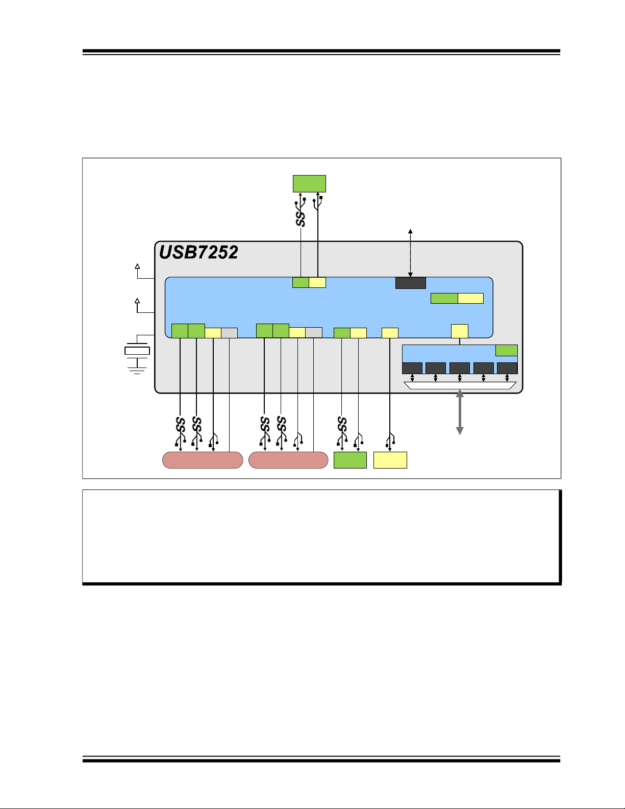
The Microchip USB7252 hub is a low-power, OEM configurable, USB 3.2 Gen 2 hub controller with 4 downstream ports
and advanced features for embedded USB applications. The USB7252 is fully compliant with the Universal Serial Bus
Revision 3.2 Specification and USB 2.0 Link Power Management Addendum. The USB7252 supports 10 Gbps SuperSpeed+ (SS+), 5 Gbps SuperSpeed (SS), 480 Mbps Hi-Speed (HS), 12 Mbps Full-Speed (FS), and 1.5 Mbps LowSpeed (LS) USB downstream devices on three standard USB 3.2 Gen 2 downstream ports and only legacy speeds (HS/
FS/LS) on one standard USB 2.0 downstream port.
The USB7252 is a standard USB 3.2 Gen 2 hub that supports native basic Type-C with integrated CC logic on two downstream ports. The downstream Type-C ports include internal USB 3.2 Gen 2 multiplexers; no external multiplexer is
required for Type-C support.
The USB7252 supports the legacy USB speeds (HS/FS/LS) through a dedicated USB 2.0 hub controller that is the culmination of seven generations of Microchip hub feature controller design and experience with proven reliability, interoperability, and device compatibility. The SuperSpeed hub controller operates in parallel with the USB 2.0 controller,
decoupling the 10/5 Gbps SS+/SS data transfers from bottlenecks due to the slower USB 2.0 traffic.
The USB7252 enables OEMs to configure their system using “Configuration Straps.” These straps simplify the configuration process assigning default values to USB 3.2 Gen 2 ports and GPIOs. OEMs can disable ports, enable battery
charging and define GPIO functions as default assignments on power up removing the need for OTP or external SPI
ROM.
The USB7252 supports downstream battery charging. The USB7252 integrated battery charger detection circuitry supports the USB-IF Battery Charging (BC1.2) detection method and most Apple devices. The USB7252 provides the battery charging handshake and supports the following USB-IF BC1.2 charging profiles:
• DCP: Dedicated Charging Port (Power brick with no data)
• CDP: Charging Downstream Port (1.5A with data)
• SDP: Standard Downstream Port (0.5A[USB 2.0]/0.9A[USB 3.2] with data)
Additionally, the USB7252 includes many powerful and unique features such as:
The Hub Feature Controller, an internal USB device dedicated for use as a USB to I
allows external circuits or devices to be monitored, controlled, or configured via the USB interface.
Multi-Host Endpoint Reflector, which provides unique USB functionality whereby USB data can be “mirrored” between
two USB hosts (Multi-Host) in order to perform a single USB transaction.This capability is fully covered by Microchip
intellectual property (U.S. Pat. Nos. 7,523,243 and 7,627,708) and is instrumental in enabling Apple CarPlay
the Apple iPhone
FlexConnect, which provides flexible connectivity options. One of the USB7252’s downstream ports can be reconfigured to become the upstream port, allowing master capable devices to control other devices on the hub.
PortSwap, which adds per-port programmability to USB differential-pair pin locations. PortSwap allows direct alignment
of USB signals (D+/D-) to connectors to avoid uneven trace length or crossing of the USB differential signals on the
PCB.
PHYBoost, which provides programmable levels of Hi-Speed USB signal drive strength
in the downstream port transceivers. PHYBoost attempts to restore USB signal integrity
in a compromised system environment. The graphic on the right shows an example of
Hi-Speed USB eye diagrams before and after PHYBoost signal integrity restoration. in
a compromised system environment.
VariSense, which controls the Hi-Speed USB receiver sensitivity enabling programmable levels of USB signal receive
sensitivity. This capability allows operation in a sub-optimal system environment, such as when a captive USB cable is
used.
Port Split, which allows for the USB 3.2 Gen 2 and USB 2.0 portions of downstream port 3 to operate independently
and enumerate two separate devices in parallel in special applications.
®
becomes a USB Host.
2
C/UART/SPI/GPIO interface that
™
, where
DS00002736D-page 6 2018 - 2020 Microchip Technology Inc.
Page 7
USB7252
Hub Controller Logic
I2C/SPI
25 Mhz
USB3 USB2
P4
A
PHY0
+3.3 V
VCORE
P3
A
PHY5 PHY2PHY5PHY1
PHY2
B
PHY1
A
PHY3
PHY4
B
PHY3
A
PHY0
P2
C
P1
C
CC
CC
Hub Feature Controller
GPIO SMB
OTP
SPI I2S
UART
Mux
HFC
PHY
I2C from Master
P0
B
The USB7252 can be configured for operation through internal default settings. Custom OEM configurations are supported through external SPI ROM or OTP ROM. All port control signal pins are under firmware control in order to allow
for maximum operational flexibility and are available as GPIOs for customer specific use.
The USB7252 is available in commercial (0°C to +70°C) and industrial (-40°C to +85°C) temperature ranges. An internal block diagram of the USB7252 in an upstream Type-C application is shown in Figure 2-1.
FIGURE 2-1: USB7252 INTERNAL BLOCK DIAGRAM - UPSTREAM TYPE-B APPLICATION
Note: All port numbering in this document is LOGICAL port numbering with the device in the default configuration.
LOGICAL port numbering is the numbering as communicated to the USB host. It is the end result after any
port number remapping or port disabling. The PHYSICAL port number is the port number with respect to
the physical PHY on the chip. PHYSICAL port numbering is fixed and the settings are not impacted by
LOGICAL port renumbering/remapping. Certain port settings are made with respect to LOGICAL port numbering, and other port settings are made with respect to PHYSICAL port numbering. Refer to the “Configuration of USB7202/USB7206/USB725x” application note for details on the LOGICAL vs. PHYSICAL
mapping and additional configuration details.
2018 - 2020 Microchip Technology Inc. DS00002736D-page 7
Page 8
USB7252
Thermal slug connects to VSS
1009998979695949392
9089888786
85
91
16
15
14
13
12
11
10
9
8
6
5
4
3
2
1
7
41
40
39
37
36
35
34
33
32
31
30
29
28
27
26
75
74
73
72
71
70
68
67
66
65
69
64
63
62
61
60
38
25
24
23
22
21
20
19
18
17
50
49
48
46
45
44
43
42
47
59
58
57
56
55
54
53
52
51
84
83
8180797877
76
82
Microchip
USB7252
(Top Vi ew 100-VQFN)
RESET_N
DP1_VBUS_MON
PF31
DP1_CC1
USB3DN_RXDM1A
USB3DN_RXDP1A
VCORE
USB3DN_TXDM1A
USB3DN_TXDP1A
USB2DN_DM1/PRT_DIS_M1
PF30
USB3DN_RXDM1B
USB2DN_DP1/PRT_DIS_P1
USB3DN_RXDP1B
VCORE
USB3DN_TXDM1B
USB3DN_TXDP1B
USB2DN_DM4/PRT_DIS_M4
USB2DN_DP4/PRT_DIS_P4
DP1_CC2
CFG_STRAP1
CFG_STRAP2
CFG_STRAP3
TESTEN
VCORE
DP2_CC1
DP2_VBUS_MON
USB3DN_RXDM2A
USB3DN_TXDM2B
USB3DN_TXDP2B
DP2_CC2
USB3DN_RXDP2A
VCORE
USB3DN_TXDP2A
USB2DN_DM2/PRT_D IS_M2
USB2DN_DP2/PRT_DIS_P2
VDD33
USB3DN_TXDM2A
PF9
VCORE
USB3DN_RXDM2B
USB3DN_RXDP2B
PF3
PF2
PF5
PF4
PF6
PF8
PF7
VDD33
PF17
SPI_D3/PF25
SPI_D0/CFG_BC_EN/PF22
SPI_ CLK/ PF21
VDD33
SPI_D1/PF23
PF19
PF26
TEST3
SPI_CE_N/CFG_NON_REM/PF20
TEST1
PF10
PF13
VDD33
TEST2
SPI_D2/PF24
PF18
PF15
PF16
VDD33
VCORE
PF12
PF29
PF11
PF14
PF27
PF28
VCORE
VCORE
USB3DN_TXDM3
USB3DN_TXDP3
USB2DN_DM3/PRT_D IS_M3
USB2DN_DP3/PRT_DIS_P3
VBUS_MON_UP
VDD33
USB3UP_TXDM
USB3UP_TXDP
USB2UP_DM
USB2UP_DP
VDD33
USB3DN_RXDM3
USB3DN_RXDP3
RBIAS
VDD33
XTALI/C LK_IN
XTALO
ATEST
USB3UP_RXDM
USB3UP_RXDP
VCORE
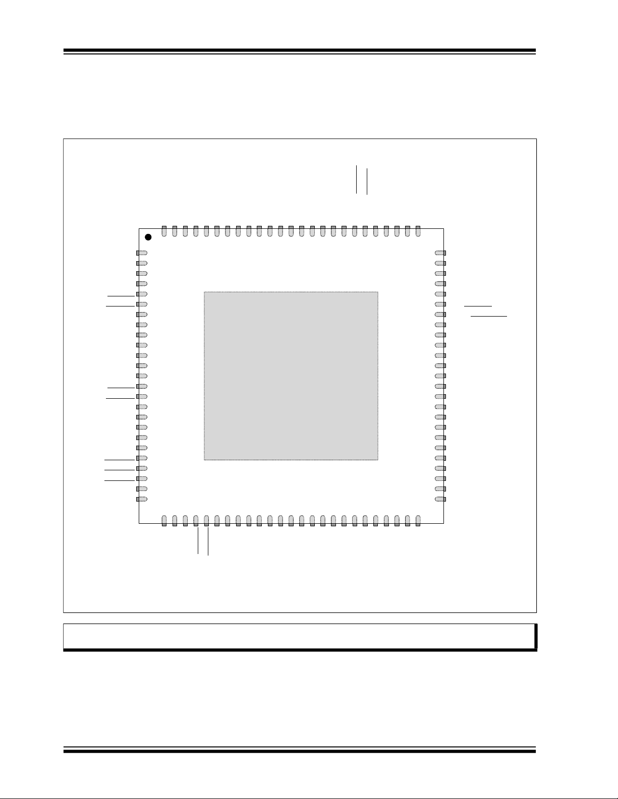
3.0 PIN DESCRIPTIONS
3.1 Pin Assignments
FIGURE 3-1: USB7252 100-VQFN PIN ASSIGNMENTS
Note: Configuration straps are identified by an underlined symbol name. Signals that function as configuration
straps must be augmented with an external resistor when connected to a load.
DS00002736D-page 8 2018 - 2020 Microchip Technology Inc.
Page 9
USB7252
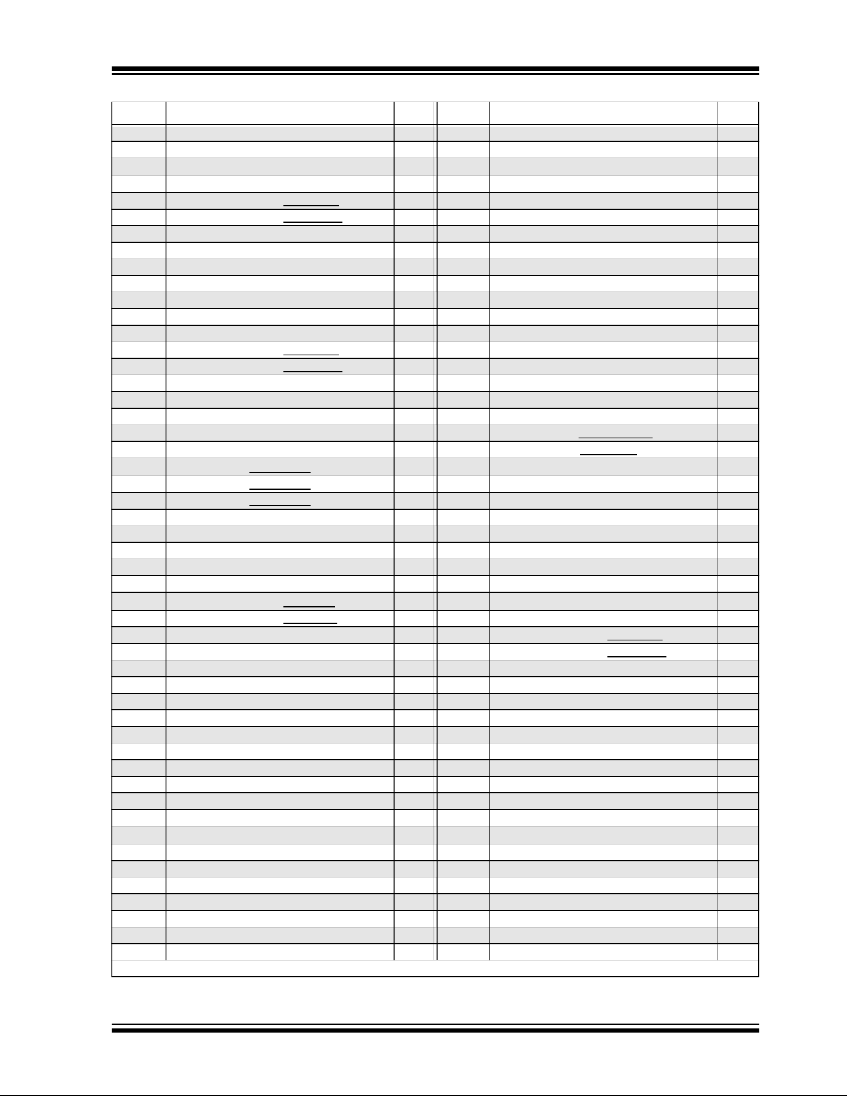
Pin Num Pin Name Reset Pin Num Pin Name Reset
1 RESET_N Z 51 PF10 PD
2 PF30 Z 52 PF11 PD
3 PF31 Z 53 VDD33 Z
4 DP1_VBUS_MON AI 54 PF12 PD
5 USB2DN_DP1/PRT_DIS_P1 AIO PD 55 VCORE Z
6 USB2DN_DM1/PRT_DIS_M1 AIO PD 56 PF13 PD
7 USB3DN_TXDP1A AO PD 57 PF14 PD
8 USB3DN_TXDM1A AO PD 58 PF15 PD
9 VCORE Z 59 PF16 PD
10 USB3DN_RXDP1A AI PD 60 PF17 PD
11 USB3DN_RXDM1A AI PD 61 PF18 Z
12 DP1_CC1 AI 62 VDD33 Z
13 DP1_CC2 AI 63 TEST1 Z
14 USB2DN_DP4/PRT_DIS_P4 AIO PD 64 TEST2 Z
15 USB2DN_DM4/PRT_DIS_M4 AIO PD 65 TEST3 Z
16 USB3DN_TXDP1B AO PD 66 PF19 Z
17 USB3DN_TXDM1B AO PD 67 VDD33 Z
18 VCORE Z 68 SPI_CLK/PF21 Z
19 USB3DN_RXDP1B AI PD 69 SPI_CE_N/CFG_NON_REM/PF20 PU
20 USB3DN_RXDM1B AI PD 70 SPI_D0/CFG_BC_EN/PF22 Z
21 CFG_STRAP1 Z 71 SPI_D1/PF23 Z
22 CFG_STRAP2 Z 72 SPI_D2/PF24 Z
23 CFG_STRAP3 Z 73 SPI_D3/PF25 Z
24 TESTEN Z 74 PF29 Z
25 VCORE Z 75 PF26 Z
26 VDD33 Z 76 PF27 Z
27 DP2_CC1 AI 77 PF28 Z
28 DP2_CC2 AI 78 VCORE Z
29 USB2DN_DP2/PRT_DIS_P2 AIO PD 79 VDD33 Z
30 USB2DN_DM2/PRT_DIS_M2 AIO PD 80 VBUS_MON_UP AI
31 USB3DN_TXDP2A AO PD 81 USB2DN_DP3/PRT_DIS_P3 AIO PD
32 USB3DN_TXDM2A AO PD 82 USB2DN_DM3/PRT_DIS_M3 AIO PD
33 VCORE Z 83 USB3DN_TXDP3 AO PD
34 USB3DN_RXDP2A AI PD 84 USB3DN_TXDM3 AO PD
35 USB3DN_RXDM2A AI PD 85 VCORE Z
36 DP2_VBUS_MON AI 86 USB3DN_RXDP3 AI PD
37 USB3DN_TXDP2B AO PD 87 USB3DN_RXDM3 AI PD
38 USB3DN_TXDM2B AO PD 88 VDD33 Z
39 VCORE Z 89 USB2UP_DP AIO Z
40 USB3DN_RXDP2B AI PD 90 USB2UP_DM AIO Z
41 USB3DN_RXDM2B AI PD 91 USB3UP_TXDP AO PD
42 VDD33 Z 92 USB3UP_TXDM AO PD
43 PF2 Z 93 VCORE Z
44 PF3 Z 94 USB3UP_RXDP AI PD
45 PF4 Z 95 USB3UP_RXDM AI PD
46 PF5 Z 96 ATEST AO
47 PF6 Z 97 XTALO AO
48 PF7 Z 98 XTALI/CLK_IN AI
49 PF8 Z 99 VDD33 Z
50 PF9 Z 100 RBIAS AI
Exposed Pad (VSS) must be connected to ground.
2018 - 2020 Microchip Technology Inc. DS00002736D-page 9
Page 10

USB7252
3.2 Pin Descriptions
This section contains descriptions of the various USB7252 pins. The “_N” symbol in the signal name indicates that the
active, or asserted, state occurs when the signal is at a low voltage level. For example, RESET_N indicates that the
reset signal is active low. When “_N” is not present after the signal name, the signal is asserted when at the high voltage
level.
The terms assertion and negation are used exclusively. This is done to avoid confusion when working with a mixture of
“active low” and “active high” signal. The term assert, or assertion, indicates that a signal is active, independent of
whether that level is represented by a high or low voltage. The term negate, or negation, indicates that a signal is inactive.
The “If Unused” column provides information on how to terminate pins if they are unused in a customer design.
Buffer type definitions are detailed in Section 1.2, Buffer Types.
TABLE 3-1: PIN DESCRIPTIONS
Name Symbol
Upstream USB
3.2 Gen 2 TX D+
Upstream USB
3.2 Gen 2 TX D-
Upstream USB
3.2 Gen 2 RX D+
Upstream USB
3.2 Gen 2 RX D-
Downstream
Port 1 USB 3.2
Gen 2 TX D+
Orientation A
Downstream
Port 1 USB 3.2
Gen 2 TX D- Ori-
entation A
USB3DN_TXDP1A I/O-U Downstream USB Type-C
USB3DN_TXDM1A I/O-U Downstream USB Type-C “Orientation A”
Buffer
Type
USB 3.2 Gen 2 Interfaces
USB3UP_TXDP I/O-U Upstream USB 3.2 Gen 2 Transmit Data
Plus.
USB3UP_TXDM I/O-U Upstream USB 3.2 Gen 2 Transmit Data
Minus.
USB3UP_RXDP I/O-U Upstream USB 3.2 Gen 2 Receive Data
Plus.
USB3UP_RXDM I/O-U Upstream USB 3.2 Gen 2 Receive Data
Minus.
SuperSpeed+ Transmit Data Plus, port 1.
SuperSpeed+ Transmit Data Minus, port 1.
Description If Unused
®
“Orientation A”
Float
Float
Weak pulldown to
GND
Weak pulldown to
GND
Float
Float
Downstream
Port 1 USB 3.2
Gen 2 RX D+
Orientation A
Downstream
Port 1 USB 3.2
Gen 2 RX DOrientation A
Downstream
Port 1 USB 3.2
Gen 2 TX D+
Orientation B
DS00002736D-page 10 2018 - 2020 Microchip Technology Inc.
USB3DN_RXDP1A I/O-U Downstream USB Type-C “Orientation A”
SuperSpeed+ Receive Data Plus, port 1.
USB3DN_RXDM1A I/O-U Downstream USB Type-C “Orientation A”
SuperSpeed+ Receive Data Minus, port 1.
USB3DN_TXDP1B I/O-U Downstream USB Type-C “Orientation B”
SuperSpeed+ Transmit Data Plus, port 1.
Weak pulldown to
GND
Weak pulldown to
GND
Float
Page 11

TABLE 3-1: PIN DESCRIPTIONS (CONTINUED)
USB7252
Name Symbol
Downstream
Port 1 USB 3.2
Gen 2 TX D-
Orientation B
Downstream
Port 1 USB 3.2
Gen 2 RX D+
Orientation B
Downstream
Port 1 USB 3.2
Gen 2 RX DOrientation B
Downstream
Port 2 USB 3.2
Gen 2 TX D+
Orientation A
Downstream
Port 2 USB 3.2
Gen 2 TX D-
Orientation A
USB3DN_TXDM1B I/O-U Downstream USB Type-C “Orientation B”
USB3DN_RXDP1B I/O-U Downstream USB Type-C “Orientation B”
USB3DN_RXDM1B I/O-U Downstream USB Type-C “Orientation B”
USB3DN_TXDP2A I/O-U Downstream USB Type-C “Orientation A”
USB3DN_TXDM2A I/O-U Downstream USB Type-C “Orientation A”
Buffer
Type
Description If Unused
SuperSpeed+ Transmit Data Minus, port 1.
SuperSpeed+ Receive Data Plus, port 1.
SuperSpeed+ Receive Data Minus, port 1.
SuperSpeed+ Transmit Data Plus, port 2.
SuperSpeed+ Transmit Data Minus, port 2.
Float
Weak pulldown to
GND
Weak pulldown to
GND
Float
Float
Downstream
Port 2 USB 3.2
Gen 2 RX D+
Orientation A
Downstream
Port 2 USB 3.2
Gen 2 RX DOrientation A
Downstream
Port 2 USB 3.2
Gen 2 TX D+
Orientation B
Downstream
Port 2 USB 3.2
Gen 2 TX D-
Orientation B
Downstream
Port 2 USB 3.2
Gen 2 RX D+
Orientation B
Downstream
Port 2 USB 3.2
Gen 2 RX DOrientation B
USB3DN_RXDP2A I/O-U Downstream USB Type-C “Orientation A”
SuperSpeed+ Receive Data Plus, port 2.
USB3DN_RXDM2A I/O-U Downstream USB Type-C “Orientation A”
SuperSpeed+ Receive Data Minus, port 2.
USB3DN_TXDP2B I/O-U Downstream USB Type-C “Orientation B”
SuperSpeed+ Transmit Data Plus, port 2.
USB3DN_TXDM2B I/O-U Downstream USB Type-C “Orientation B”
SuperSpeed+ Transmit Data Minus, port 2.
USB3DN_RXDP2B I/O-U Downstream USB Type-C “Orientation B”
SuperSpeed+ Receive Data Plus, port 2.
USB3DN_RXDM2B I/O-U Downstream USB Type-C “Orientation B”
SuperSpeed+ Receive Data Minus, port 2.
Weak pulldown to
GND
Weak pulldown to
GND
Float
Float
Weak pulldown to
GND
Weak pulldown to
GND
2018 - 2020 Microchip Technology Inc. DS00002736D-page 11
Page 12
USB7252
TABLE 3-1: PIN DESCRIPTIONS (CONTINUED)
Name Symbol
Downstream
Port 3 USB 3.2
Gen 2 TX D+
Downstream
Port 3 USB 3.2
Gen 2 TX D-
Downstream
Port 3 USB 3.2
Gen 2 RX D+
Downstream
Port 3 USB 3.2
Gen 2 RX D-
Upstream USB
2.0 D+
Upstream USB
2.0 D-
Downstream
Ports 1-4 USB
2.0 D+
USB3DN_TXDP3 I/O-U Downstream SuperSpeed+ Transmit Data
USB3DN_TXDM3 I/O-U Downstream SuperSpeed+ Transmit Data
USB3DN_RXDP3 I/O-U Downstream SuperSpeed+ Receive Data
USB3DN_RXDM3 I/O-U Downstream SuperSpeed+ Receive Data
USB2DN_DP[1:4] I/O-U Downstream USB 2.0 Ports 1-4 Data Plus
Buffer
Type
Plus, port 3.
Minus, port 3.
Plus, port 3.
Minus, port 3.
USB 2.0 Interfaces
USB2UP_DP I/O-U Upstream USB 2.0 Data Plus (D+). Mandatory
USB2UP_DM I/O-U Upstream USB 2.0 Data Minus (D-). Mandatory
(D+).
Description If Unused
Float
Float
Weak pulldown to
GND
Weak pulldown to
GND
Note 3-12
Note 3-12
Connect
directly to
3.3V
Downstream
Ports 1-4 USB
2.0 D-
SPI Clock SPI_CLK I/O-U SPI clock. If the SPI interface is enabled,
SPI Data 3-0 SPI_D[3:0] I/O-U SPI Data 3-0. If the SPI interface is enabled,
USB2DN_DM[1:4] I/O-U Downstream USB 2.0 Ports 1-4 Data Minus
(D-)
SPI Interface
this pin must be driven low during reset.
these signals function as Data 3 through 0.
Note 3-1 SPI_D0 operates as the
CF G _ BC _E N
external SPI memory is not
used. It must be terminated
wit h t h e sel e c t ed st r a p
resistor to 3.3V or GND.
SP I _ D[ 1 : 3 ] sh o u l d b e
connected to GND through
a weak pull-down.
s t r a p if
Connect
directly to
3.3V
Weak pulldown to
GND
Note 3-1
DS00002736D-page 12 2018 - 2020 Microchip Technology Inc.
Page 13
TABLE 3-1: PIN DESCRIPTIONS (CONTINUED)
VBUS_P1
43K
49.9K
DP1_VBUS_MON
USB7252
Name Symbol
SPI Chip
Enable
Downstream
Port 1 Type-C
Voltage Monitor
DP1_VBUS_MON AIO Used to detect Type-C VBUS vSafe5V and
Buffer
Type
SPI_CE_N I/O12 Active low SPI chip enable input. If the SPI
interface is enabled, this pin must be driven
high in powerdown states.
Note 3-2 Operates as the
USB Type-C Connector Control
vSafe0V states on Port 1. A nominal voltage
of 2.7V (2.4V min -3.0V max) is required to
detect the presence of vSafe5V.
Externally, VBUS can be as high as 5.25 V,
which can be damaging to this pin. The
amplitude of VBUS must be reduced by a
voltage divider. The recommended voltage
divider is shown below. 1% tolerance resistors are recommended.
Description If Unused
CFG_NO N _REM
external SPI memory is not
used. It must be terminated
wit h t h e sel e c t ed st r ap
resistor to 3.3V or GND.
str ap if
Note 3-2
Note 3-3
Downstream
Port 1 Type-C
CC1
For proper Type-C port operation, it is critical that this pin actually be connected to
VBUS of the port through the recommended
resistor divider. This pin should not be tied
permanently to a fixed voltage power rail.
Note 3-3 If unused: Weak pull-down
to GND. This pin may be
le ft unu s e d if Port 1 is
disabled or reconfigured to
ope rate in legacy Type-A
m o d e th r o ug h hu b
configuration.
DP1_CC1 I/O12 Used for Type-C attach and orientation
detection on Port 1. Includes configurable
Rp/Ra selection. Connect this pin directly to
the CC1 pin of the respective Type-C connector.
Note 3-4 If unused: Weak pull-down
to GND. This pin may only
be left unused if Port 1 is
disabled or reconfigured to
ope rate in legacy Type-A
m o d e th r o ug h hu b
configuration.
Note 3-4
2018 - 2020 Microchip Technology Inc. DS00002736D-page 13
Page 14
USB7252
VBUS_P2
43K
49.9K
DP2_VBUS_MON
TABLE 3-1: PIN DESCRIPTIONS (CONTINUED)
Name Symbol
Downstream
Port 1 Type-C
CC2
Downstream
Port 2 Type-C
Voltage Monitor
DP2_VBUS_MON AIO Used for detect Type-C VBUS vSafe5V and
Buffer
Type
DP1_CC2 I/O12 Used for Type-C attach and orientation
detection on Port 1. Includes configurable
Rp/Ra selection. Connect this pin directly to
the CC2 pin of the respective Type-C connector.
Note 3-5 If unused: Weak pull-down
vSafe0V states on Port 2. A nominal voltage of 2.7V (2.4V min -3.0V max) is
required to detect the presence of vSafe5V.
Externally, VBUS can be as high as 5.25 V,
which can be damaging to this pin. The
amplitude of VBUS must be reduced by a
voltage divider. The recommended voltage
divider is shown below. 1% tolerance resistors are recommended.
Description If Unused
to GND. This pin may only
be left unused if Port 1 is
disabled or reconfigured to
ope rate in legacy Type-A
m o d e th r o ug h hu b
configuration.
Note 3-5
Note 3-6
Downstream
Port 2 Type-C
CC1
For proper Type-C port operation, it is critical that this pin actually be connected to
VBUS of the port through the recommended
resistor divider. This pin should not be tied
permanently to a fixed voltage power rail.
Note 3-6 If unused: Weak pull-down
to GND. This pin may be
le ft unu s e d if Port 2 is
disabled or reconfigured to
ope rate in legacy Type-A
m o d e th r o ug h hu b
configuration.
DP2_CC1 I/O12 Used for Type-C attach and orientation
detection on Port 2. Includes configurable
Rp/Ra selection. Connect this pin directly to
the CC1 pin of the respective Type-C connector.
Note 3-7 If unused: Weak pull-down
to GND. This pin may only
be left unused if Port 2 is
disabled or reconfigured to
ope rate in legacy Type-A
m o d e th r o ug h hu b
configuration.
Note 3-7
DS00002736D-page 14 2018 - 2020 Microchip Technology Inc.
Page 15

TABLE 3-1: PIN DESCRIPTIONS (CONTINUED)
VBUS_UP
43K
49.9K
VBUS_MON_UP
USB7252
Name Symbol
Downstream
Port 2 Type-C
CC2
Upstream
Voltage Monitor
VBUS_MON_UP I/O12 Used to detect VBUS on the upstream port.
Buffer
Type
DP2_CC2 I/O12 Used for Type-C attach and orientation
detection on Port 2. Includes configurable
Rp/Ra selection. Connect this pin directly to
the CC2 pin of the respective Type-C connector.
Note 3-8 If unused: Weak pull-down
Externally, VBUS can be as high as 5.25 V,
which can be damaging to this pin. A nominal voltage of 2.7V (2.4V min -3.0V max) is
required to detect the presence of vSafe5V.
The amplitude of VBUS must be reduced by
a voltage divider. The recommended voltage
divider is shown below. 1% tolerance resistors are recommended.
Description If Unused
to GND. This pin may only
be left unused if Port 2 is
disabled or reconfigured to
ope rate in legacy Type-A
m o d e th r o ug h hu b
configuration.
Note 3-8
Mandatory
Note 3-12
Programmable
Function Pins
Note: For embedded host applications,
this pin should be controlled by
an I/O on the host processor to a
2.68V logic level.
Miscellaneous
PF[31:2] I/O12 Programmable function pins.
Note 3-9 If unused: depends on the
co n fi g ure d pin functi on.
Ref e r to S e c t io n 3. 3 .4 ,
PF [ 3 1 : 2 ] C o n f i g ur a ti on
(CFG_STRAP[2:1])
Note 3-9
2018 - 2020 Microchip Technology Inc. DS00002736D-page 15
Page 16

USB7252
TABLE 3-1: PIN DESCRIPTIONS (CONTINUED)
Name Symbol
Test 1 TEST1 A Test 1 pin.
Test 2 TEST2 A Test 2 pin.
Test 3 TEST3 A Test 3 pin.
Reset Input RESET_N IS This active low signal is used by the system
Bias Resistor RBIAS I-R A 12.0 k
Buffer
Type
Description If Unused
This signal is used for test purposes and
must always be pulled-up to 3.3V via a 10
k
resistor.
This signal is used for test purposes and
must always be pulled-up to 3.3V via a 10
k
resistor.
This signal is used for test purposes and
must always be pulled-up to 3.3V via a 10
k
resistor.
to reset the device.
1.0% resistor is attached from
ground to this pin to set the transceiver’s
internal bias settings. Place the resistor as
close the device as possible with a dedicated, low impedance connection to the
ground plane.
Pull to 3.3V
through a
10 k
resistor
Pull to 3.3V
through a
10 k
resistor
Pull to 3.3V
through a
10 k
resistor
Mandatory
Note 3-12
Mandatory
Note 3-12
Test TESTEN I/O12 Test pin.
This signal is used for test purposes and
must always be connected to ground.
Analog Test ATEST A Analog test pin.
This signal is used for test purposes and
must always be left unconnected.
External 25 MHz
Crystal Input
External 25 MHz
Reference Clock
Input
XTALI ICLK External 25 MHz crystal input Mandatory
CLK_IN ICLK External reference clock input.
The device may alternatively be driven by a
single-ended clock oscillator. When this
method is used, XTALO should be left
unconnected.
Connect to
GND
Float
Note 3-12
Mandatory
Note 3-12
DS00002736D-page 16 2018 - 2020 Microchip Technology Inc.
Page 17
TABLE 3-1: PIN DESCRIPTIONS (CONTINUED)
USB7252
Name Symbol
External 25 MHz
Crystal Output
Port 4-1 D+
Disable
Configuration
Strap
Buffer
Type
XTALO OCLK External 25 MHz crystal output Float
Configuration Straps
PRT_DIS_P[
4:1] I Port 4-1 D+ Disable Configuration Strap.
These configuration straps are used in conjunction with the corresponding
PRT_DIS_M[
related port (4-1). See Note 3-13.
Both USB data pins for the corresponding
port must be tied to 3.3V to disable the
associated downstream port.
Description If Unused
4:1] straps to disable the
(only if single-ended
clock is
connected
to
CLK_IN)
N/A
Port 4-1 D-
Disable
Configuration
Strap
Non-Removable
Ports
Configuration
Strap
PRT_DIS_M[
CFG_NON_REM
4:1] I Port 4-1 D- Disable Configuration Strap.
These configuration straps are used in conjunction with the corresponding
PRT_DIS_P[
related port (4-1). See Note 3-13.
Both USB data pins for the corresponding
port must be tied to 3.3V to disable the
associated downstream port.
I Non-Removable Ports Configuration Strap.
This configuration strap controls the number
of reported non-removable ports. See
Note 3-13 .
Note 3-10 Mandatory if external SPI
4:1] straps to disable the
me mor y is not us e d for
f i r m w a r e e x e c u t i o n . I f
ext e r na l S P I memory is
us e d f o r f i rm w a re
ex e c u t i o n, t he n
configuration strap resistor
should be omitted.
Mandatory
Note 3-12
Note 3-10
2018 - 2020 Microchip Technology Inc. DS00002736D-page 17
Page 18

USB7252
TABLE 3-1: PIN DESCRIPTIONS (CONTINUED)
Name Symbol
Battery Charging
Configuration
Strap
Device Mode
Configuration
Straps 3-1
+3.3V I/O Power
Supply Input
CFG_STRAP[3:1]
Buffer
Type
CFG_BC_EN
VDD33 P +3.3 V power and internal regulator input. Mandatory
I/O12 Battery Charging Configuration Strap.
This configuration strap controls the number
of BC 1.2 enabled downstream ports. See
Note 3-13.
Note 3-11 Mandatory if external SPI
I Device Mode Configuration Straps 3-1.
These configuration straps are used to
select the device’s mode of operation. See
Note 3-13.
Power/Ground
Description If Unused
Mandatory
Note 3-12
me mor y is not us e d for
f i r m w a r e e x e c u t i o n . I f
ex t e r na l S P I memory is
us e d f o r f i rm w a re
ex e c u t i o n, t he n
configuration strap resistor
should be omitted.
Mandatory
Note 3-12
Note 3-12
Digital Core
Power Supply
Input
Ground VSS P Common ground.
Note 3-12 Configuration strap values are latched on Power-On Reset (POR) and the rising edge of RESET_N
(external chip reset). Configuration straps are identified by an underlined symbol name. Signals that
function as configuration straps must be augmented with an external resistor when connected to a
load. For additional information, refer to Section 3.3, Configuration Straps and Programmable
Functions.
Note 3-13 Pin use is mandatory. Cannot be left unused.
VCORE P Digital core power supply input. Mandatory
Note 3-12
Mandatory
Note 3-12
This exposed pad must be connected to the
ground plane with a via array.
3.3 Configuration Straps and Programmable Functions
Configuration straps are multi-function pins that are used during Power-On Reset (POR) or external chip reset
(RESET_N) to determine the default configuration of a particular feature. The state of the signal is latched following
deassertion of the reset. Configuration straps are identified by an underlined symbol name. This section details the various device configuration straps and associated programmable pin functions.
Note: The system designer must guarantee that configuration straps meet the timing requirements specified in
Section 9.6.2, Power-On and Configuration Strap Timing and Section 9.6.3, Reset and Configuration Strap
Timing. If configuration straps are not at the correct voltage level prior to being latched, the device may
capture incorrect strap values.
DS00002736D-page 18 2018 - 2020 Microchip Technology Inc.
Page 19
USB7252
3.3.1 PORT DISABLE CONFIGURATION (PRT_DIS_P[4:1] / PRT_DIS_M[4:1])
The PRT_DIS_P[4:1] / PRT_DIS_M[4:1] configuration straps are used in conjunction to disable the related port (4-1)
For PRT_DIS_P
0 = Port x D+ Enabled
1 = Port x D+ Disabled
For PRT_DIS_M
0 = Port x D- Enabled
1 = Port x D- Disabled
x (where x is the corresponding port 4-1):
x (where x is the corresponding port 4-1):
Note: Both PRT_DIS_P
the associated downstream port. Disabling the USB 2.0 port will also disable the corresponding USB 3.0
port.
x and PRT_DIS_Mx (where x is the corresponding port) must be tied to 3.3 V to disable
3.3.2 NON-REMOVABLE PORT CONFIGURATION (CFG_NON_REM)
The CFG_NON_REM configuration strap is used to configure the non-removable port settings of the device to one of
five settings. These modes are selected by the configuration of an external resistor on the CFG_NON_REM
resistor options are a 200 kΩ pull-down, 200 kΩ pull-up, 10 kΩ pull-down, 10 kΩ pull-up, and 10 Ω pull-down, as shown
in Table 3-2.
pin. The
3.3.3 BATTERY CHARGING CONFIGURATION (CFG_BC_EN)
TABLE 3-2: CFG_NON_REM RESISTOR ENCODING
CFG_NON_REM Resistor Value Setting
200 kΩ Pull-Down All ports removable
200 kΩ Pull-Up Port 1 non-removable
10 kΩ Pull-Down Ports 1, 2 non-removable
10 kΩ Pull-Up Ports 1, 2, 3 non-removable
10 Ω Pull-Down Ports 1, 2, 3, 4 non-removable
The CFG_BC_EN configuration strap is used to configure the battery charging port settings of the device to one of five
settings. These modes are selected by the configuration of an external resistor on the CFG_BC_EN
options are a 200 kΩ pull-down, 200 kΩ pull-up, 10 kΩ pull-down, 10 kΩ pull-up, and 10 Ω pull-down, as shown in
Table 3-3.
pin. The resistor
TABLE 3-3: CFG_BC_EN RESISTOR ENCODING
CFG_BC_EN Resistor Value Setting
200 kΩ Pull-Down Battery charging not enable on any port
200 kΩ Pull-Up BC1.2 DCP and CDP battery charging enabled on Port 1
10 kΩ Pull-Down BC1.2 DCP and CDP battery charging enabled on Ports 1, 2
10 kΩ Pull-Up BC1.2 DCP and CDP battery charging enabled on Ports 1, 2, 3
10 Ω Pull-Down BC1.2 DCP and CDP battery charging enabled on Ports 1, 2, 3, 4
3.3.4 PF[31:2] CONFIGURATION (CFG_STRAP[2:1])
The USB7252 provides 30 programmable function pins (PF[31:2]). These pins can be configured to 4 predefined configurations via the CFG_STRAP[2:1]
CFG_STRAP[2:1]
and should not be used.
2018 - 2020 Microchip Technology Inc. DS00002736D-page 19
pins, as detailed in Table 3-4. Resistor values and combinations not detailed in Table 3-4 are reserved
pins. These configurations are selected via external resistors on the
Page 20

USB7252
Note: CFG_STRAP3
is not used and must be pulled-down to ground via a 200 k resistor.
TABLE 3-4: CFG_STRAP[2:1] RESISTOR ENCODING
Mode
CFG_STRAP2
Resistor Value
Configuration 1 200 kΩ Pull-Down 200 kΩ Pull-Down
Configuration 2 200 kΩ Pull-Down 200 kΩ Pull-Up
Configuration 3 200 kΩ Pull-Down 10 kΩ Pull-Down
Configuration 4 200 kΩ Pull-Down 10 kΩ Pull-Up
A summary of the configuration pin assignments for each of the 4 configurations is provided in Table 3-5. For details on
behavior of each programmable function, refer to Table 3-6.
CFG_STRAP1
Resistor Value
TABLE 3-5: PF[31:2] FUNCTION ASSIGNMENT
Pin
Configuration 1
(SMBus/I
2
C)
PF2 DP1_VCONN1 DP1_VCONN1 DP1_VCONN1 DP1_VCONN1
PF3 DP1_VCONN2 DP1_VCONN2 DP1_VCONN2 DP1_VCONN2
PF4 DP2_DISCHARGE DP2_DISCHARGE DP2_DISCHARGE DP2_DISCHARGE
PF5 DP1_DISCHARGE DP1_DISCHARGE DP1_DISCHARGE DP1_DISCHARGE
PF6 GPIO70 GPIO70 UART_RX GPIO70
PF7 GPIO71 MIC_DET UART_TX GPIO71
(
) (
PF8
PF9
Note 3-1
(
) (
Note 3-1
PF10 DP2_VCONN1 DP2_VCONN1 DP2_VCONN1 DP2_VCONN1
PF11 DP2_VCONN2 DP2_VCONN2 DP2_VCONN2 DP2_VCONN2
PF12 PRT_CTL3_U3 PRT_CTL3_U3 PRT_CTL3_U3 PRT_CTL3_U3
PF13 PRT_CTL3 PRT_CTL3 PRT_CTL3 PRT_CTL3
PF14 GPIO78 I2S_SDI UART_nCTS GPIO78
PF15 PRT_CTL2 PRT_CTL2 PRT_CTL2 PRT_CTL2
PF16 PRT_CTL4 PRT_CTL4 PRT_CTL4 PRT_CTL4
PF17 PRT_CTL1 PRT_CTL1 PRT_CTL1 PRT_CTL1
(
) (
PF18
Note 3-1
PF19 SLV_I2C_DATA I2S_SDO UART_nRTS GPIO83
PF20 SPI_CE_N SPI_CE_N SPI_CE_N SPI_CE_N
PF21 SPI_CLK SPI_CLK SPI_CLK SPI_CLK
PF22 SPI_D0 SPI_D0 SPI_D0 SPI_D0
PF23 SPI_D1 SPI_D1 SPI_D1 SPI_D1
PF24 SPI_D2 SPI_D2 SPI_D2 SPI_D2
PF25 SPI_D3 SPI_D3 SPI_D3 SPI_D3
PF26 SLV_I2C_CLK I2S_SCK UART_nDSR GPIO90
PF27 GPIO91 I2S_MCLK UART_nDTR GPIO91
PF28 GPIO92 I2S_LRCK UART_nDCD GPIO92
(
) (
PF29
Note 3-1
PF30 MSTR_I2C_CLK MSTR_I2C_CLK MSTR_I2C_CLK MSTR_I2C_CLK
PF31 MSTR_I2C_DATA MSTR_I2C_DATA MSTR_I2C_DATA MSTR_I2C_DATA
Configuration 2
(I2S)
) (
Note 3-1
) (
Note 3-1
) (
Note 3-1
) (
Note 3-1
Configuration 3
(UART)
) (
Note 3-1
) (
Note 3-1
) (
Note 3-1
) (
Note 3-1
Configuration 4
(GPIO & FlexConnect)
)
Note 3-1
)
Note 3-1
)
Note 3-1
)
Note 3-1
DS00002736D-page 20 2018 - 2020 Microchip Technology Inc.
Page 21

USB7252
Note 3-1 The default function is not used in the USB7252.
Note: The default PFx pin functions can be overridden with additional configuration by modification of the pin mux
registers. These changes can be made during the SMBus configuration stage, by programming to OTP
memory, or during runtime (after hub has attached and enumerated) by register writes via the SMBus slave
interface or USB commands to the internal Hub Feature Controller Device.
2018 - 2020 Microchip Technology Inc. DS00002736D-page 21
Page 22

USB7252
TABLE 3-6: PROGRAMMABLE FUNCTIONS DESCRIPTIONS
Function
MSTR_I2C_CLK I/O12 Bridging Master SMBus/I
MSTR_I2C_DATA I/O12 Bridging Master SMBus/I
SLV_I2C_CLK I/O12 Slave SMBus/I
SLV_I2C_DATA I/O12 Slave SMBus/I
Buffer
Type
Description If Unused
Master SMBus/I
2
C Interface
2
C controller clock (SMBus/I2C controller
1). External 1k-10k pull-up resistors to 3.3V are required if the I
Master Interface is to be used.
2
C controller data (SMBus/I2C controller
1). External 1k-10k pull-up resistors to 3.3V are required if the I
Master Interface is to be used.
Slave SMBus/I
2
C controller clock (SMBus/I2C controller 2). Exter-
nal 1k-10k pull-up resistors to 3.3V are required if the I
2
C Interface
2
C Slave
Interface is to be used.
2
C controller data (SMBus/I2C controller 2). External
1k-10k pull-up resistors to 3.3V are required if the I
2
C Slave Inter-
face is to be used.
2
C
2
C
Weak pulldown to
GND
Weak pulldown to
GND
Weak pulldown to
GND
Weak pulldown to
GND
UART Interface
UART_TX O12 UART Transmit Weak pull-
down to
GND
UART_RX I UART Receive Weak pull-
down to
GND
UART_nCTS I UART Clear To Send Weak pull-
down to
GND
UART_nRTS O12 UART Request To Send Weak pull-
down to
GND
UART_nDCD I UART Data Carrier Detect Weak pull-
down to
GND
UART_nDSR I UART Data Set Ready Weak pull-
down to
GND
UART_nDTR O12 UART Data Terminal Ready Weak pull-
down to
GND
2
I
S Interface
I2S_SDI I I
2
S Serial Data In Weak pull-
down to
GND
DS00002736D-page 22 2018 - 2020 Microchip Technology Inc.
Page 23

TABLE 3-6: PROGRAMMABLE FUNCTIONS DESCRIPTIONS (CONTINUED)
USB7252
Function
I2S_SDO O12 I2S Serial Data Out Weak pull-
I2S_SCK O12 I
I2S_LRCK O12 I
I2S_MCLK O12 I
MIC_DET I I
DP2_VCONN1 I/O12 Port 2 VCONN1 enable. Active high signal.
Buffer
Type
Description If Unused
down to
GND
2
S Continuous Serial Clock Weak pull-
down to
GND
2
S Word Select / Left-Right Clock Weak pull-
down to
GND
2
S Master Clock Weak pull-
down to
GND
2
S Microphone Plug Detect
0 = No microphone plugged into the audio jack
1 = Microphone plugged into the audio jack
Miscellaneous
0 = VCONN is turned off.
1 = VCONN is turned on. If DP2_VCONN1 is asserted and >3.0V is
not sensed on the CC1 line, a VCONN fault condition is detected.
Note 3-1 This pin can be left unused only if Port 2 is
disabled or reconfigured to operate as a legacy
Type-A port via OTP/SMBus/SPI configuration.
Weak pulldown to
GND
Weak pulldown to
GND
(Note 3-1)
DP2_VCONN2 I/O12 Port 2 VCONN2 enable. Active high signal.
0 = VCONN is turned off.
1 = VCONN is turned on. If DP2_VCONN2 is asserted and >3.0V is
not sensed on the CC2 line, a VCONN fault condition is detected.
Note 3-2 This pin can be left unused only if Port 2 is
disabled or reconfigured to operate as a legacy
Type-A port via OTP/SMBus/SPI configuration.
DP2_DISCHARGE I/O12 Port 2 DISCHARGE enable. Active high signal.
0 = VBUS discharging is not active.
1 = VBUS is being discharged to GND. This pin only asserts for a
short duration when VBUS is being discharged from 5V (vSafe5V)
to 0V (vSafe0V).
Note 3-3 This pin can be left unused only if Port 2 is
disabled or reconfigured to operate as a legacy
Type-A port via OTP/SMBus/SPI configuration.
Weak pulldown to
GND
(Note 3-2)
Weak pulldown to
GND
(Note 3-3)
2018 - 2020 Microchip Technology Inc. DS00002736D-page 23
Page 24

USB7252
TABLE 3-6: PROGRAMMABLE FUNCTIONS DESCRIPTIONS (CONTINUED)
Function
DP1_VCONN1 I/O12 Port 1 VCONN1 enable. Active high signal.
DP1_VCONN2 I/O12 Port 1 VCONN2 enable. Active high signal.
DP1_DISCHARGE I/O12 Port 1 DISCHARGE enable. Active high signal.
Buffer
Type
Description If Unused
0 = VCONN is turned off.
1 = VCONN is turned on. If DP1_VCONN1 is asserted and >3.0V is
not sensed on the CC1 line, a VCONN fault condition is detected.
Note 3-4 This pin can be left unused only if Port 1 is
disabled or reconfigured to operate as a legacy
Type-A port via OTP/SMBus/SPI configuration.
0 = VCONN is turned off.
1 = VCONN is turned on. If DP1_VCONN2 is asserted and >3.0V is
not sensed on the CC2 line, a VCONN fault condition is detected.
Note 3-5 This pin can be left unused only if Port 1 is
disabled or reconfigured to operate as a legacy
Type-A port via OTP/SMBus/SPI configuration.
0 = VBUS discharging is not active.
1 = VBUS is being discharged to GND. This pin only asserts for a
short duration when VBUS is being discharged from 5V (vSafe5V)
to 0V (vSafe0V).
Note 3-6 This pin can be left unused only if Port 1 is
disabled or reconfigured to operate as a legacy
Type-A port via OTP/SMBus/SPI configuration.
Weak pulldown to
GND
(Note 3-4)
Weak pulldown to
GND
(Note 3-5)
Weak pulldown to
GND
(Note 3-6)
PRT_CTL4 I/O12
(PU)
Port 4 power enable / overcurrent sense
When the downstream port is enabled, this pin is set as an input
with an internal pull-up resistor applied. The internal pull-up
enables power to the downstream port while the pin monitors for an
active low overcurrent signal assertion from an external current
monitor on USB port 4.
This pin will change to an output and be driven low when the port is
disabled by configuration or by the host control.
Note: This signal controls both the USB 2.0 and USB 3.2 por-
tions of the port.
Note 3-7 This pin can be left unused only if Port 4 is
disabled via strap/OTP/SMBus/SPI configuration.
Float
(Note 3-7)
DS00002736D-page 24 2018 - 2020 Microchip Technology Inc.
Page 25

TABLE 3-6: PROGRAMMABLE FUNCTIONS DESCRIPTIONS (CONTINUED)
USB7252
Function
PRT_CTL3 I/O12
PRT_CTL2 I/O12
Buffer
Type
(PU)
(PU)
Description If Unused
Port 3 power enable / overcurrent sense
When the downstream port is enabled, this pin is set as an input
with an internal pull-up resistor applied. The internal pull-up
enables power to the downstream port while the pin monitors for an
active low overcurrent signal assertion from an external current
monitor on USB port 3.
This pin will change to an output and be driven low when the port is
disabled by configuration or by the host control.
Note: When PortSplit is disabled, this signal controls both the
USB 2.0 and USB 3.2 portions of the port. When
PortSplit is enabled, this signal controls the USB 2.0
portion of the port only.
Note 3-8 This pin can be left unused only if Port 3 is
disabled via strap/OTP/SMBus/SPI configuration.
Port 2 power enable / overcurrent sense
When the downstream port is enabled, this pin is set as an input
with an internal pull-up resistor applied. The internal pull-up
enables power to the downstream port while the pin monitors for an
active low overcurrent signal assertion from an external current
monitor on USB port 2.
Float
(Note 3-8)
Float
(Note 3-9)
PRT_CTL1 I/O12
(PU)
This pin will change to an output and be driven low when the port is
disabled by configuration or by the host control.
Note: This signal controls both the USB 2.0 and USB 3.2 por-
tions of the port.
Note 3-9 This pin can be left unused only if Port 2 is
disabled via strap/OTP/SMBus/SPI configuration.
Port 1 power enable / overcurrent sense
When the downstream port is enabled, this pin is set as an input
with an internal pull-up resistor applied. The internal pull-up
enables power to the downstream port while the pin monitors for an
active low overcurrent signal assertion from an external current
monitor on USB port 1.
This pin will change to an output and be driven low when the port is
disabled by configuration or by the host control.
Note: This signal controls both the USB 2.0 and USB 3.2 por-
tions of the port.
Note 3-10 This pin can be left unused only if Port 1 is
disabled via strap/OTP/SMBus/SPI configuration.
Float
(Note 3-9)
2018 - 2020 Microchip Technology Inc. DS00002736D-page 25
Page 26

USB7252
TABLE 3-6: PROGRAMMABLE FUNCTIONS DESCRIPTIONS (CONTINUED)
Function
PRT_CTL3_U3 O12 Port 3 USB 3.2 PortSplit power enable
GPIOx I/O12 General Purpose Inputs/Outputs
Buffer
Type
Description If Unused
This signal is an active high control signal used to enable to the
USB 3.2 portion of the downstream port 3 when PortSplit is
enabled. When PortSplit is disabled, this pin is not used.
Note: This signal should only be used to control an embedded
USB 3.2 device.
(x = 70-71, 78, 83, 90-92)
Float
Weak pulldown to
GND
3.4 Physical and Logical Port Mapping
The USB72xx family of devices are based upon a common architecture, but all have different modifications and/or pin
bond outs to achieve the various device configurations. The base chip is composed of a total of 6 USB3 PHYs and 7
USB2 PHYs. These PHYs are physically arranged on the chip in a certain way, which is referred to as the PHYSICAL
port mapping.
The actual port numbering is remapped by default in different ways on each device in the family. This changes the way
that the ports are numbered from the USB host’s perspective. This is referred to as LOGICAL mapping.
The various configuration options available for these devices may, at times, be with respect to PHYSICAL mapping or
LOGICAL mapping. Each individual configuration option which has a PHYSICAL or LOGICAL dependency is declared
as such within the register description.
The PHYSICAL vs. LOGICAL mapping is described for all port related pins in Table 3-7. A system design in schematics
and layout is generally performed using the pinout in Section 3.1, Pin Assignments, which is assigned by the default
LOGICAL mapping. Hence, it may be necessary to cross reference the PHYSICAL vs. LOGICAL look up tables when
determining the hub configuration.
Note: The MPLAB Connect tool makes configuration simple; the settings can be selected by the user with respect
to the LOGICAL port numbering. The tool handles the necessary linking to the PHYSICAL port settings.
Refer to Section 6.0, Device Configuration for additional information.
DS00002736D-page 26 2018 - 2020 Microchip Technology Inc.
Page 27

USB7252
TABLE 3-7: USB7252 PHYSICAL VS. LOGICAL PORT MAPPING
Device
Pin
5 USB2DN_DP1 X X
6 USB2DN_DM1 X X
7 USB3DN_TXDP1A X X
8 USB3DN_TXDM1A X X
10 USB3DN_RXDP1A X X
11 USB3DN_RXDM1A X X
14 USB2DN_DP4 X X
15 USB2DN_DM4 X X
16 USB3DN_TXDP1B X X
17 USB3DN_TXDM1B X X
19 USB3DN_RXDP1B X X
20 USB3DN_RXDM1B X X
29 USB2DN_DP2 X X
30 USB2DN_DM2 X X
31 USB3DN_TXDP2A X X
32 USB3DN_TXDM2A X X
34 USB3DN_RXDP2A X X
35 USB3DN_RXDM2A X X
37 USB3DN_TXDP2B X X
38 USB3DN_TXDM2B X X
40 USB3DN_RXDP2B X X
41 USB3DN_RXDM2B X X
81 USB2DN_DP3 X X
82 USB2DN_DM3 X X
83 USB3DN_TXDP3 X X
84 USB3DN_TXDM3 X X
86 USB3DN_RXDP3 X X
87 USB3DN_RXDM3 X X
89 USB2UP_DP X X
90 USB2UP_DM X X
91 USB3UP_TXDP X X
92 USB3UP_TXDM X X
94 USB3UP_RXDP X X
95 USB3UP_RXDM X X
Pin Name (as in datasheet)
LOGICAL PORT NUMBER PHYSICAL PORT NUMBER
0 1 2 3 4 0 1 2 3 4 5 6
2018 - 2020 Microchip Technology Inc. DS00002736D-page 27
Page 28

USB7252
+3.3V
Supply
USB7252
3.3V Internal Logic
VDD33 (x8 )
VSS (exposed pad)
Digital Core
Internal Logic
VCORE (x9 )
VCORE
Supply
+3.3V
0.1uF
0.001uF
x8
+3.3V
4.7uF
VCORE
0.1uF
0.001uF
x9
VCORE
4.7uF
USB7252
SPI_CE_N
SPI_CLK
SPI_D0
SPI_D1
Quad-SPI Flash
CE#
CLK
SIO0
SIO1
SPI_D2
SPI_D3
SIO2/WPn
SIO3/HOLDn
+3.3V
10K
4.0 DEVICE CONNECTIONS
4.1 Power Connections
Figure 4-1 illustrates the device power connections.
FIGURE 4-1: POWER CONNECTIONS
4.2 SPI Flash Connections
Figure 4-2 illustrates the Quad-SPI flash connections.
FIGURE 4-2: QUAD-SPI FLASH CONNECTIONS
DS00002736D-page 28 2018 - 2020 Microchip Technology Inc.
Page 29

4.3 SMBus/I2C Connections
+3.3V
USB7252
x_I2C_CLK
x_I2C_DAT
SMBus/I2C
Clock
Data
4.7K
+3.3V
4.7K
USB7252
I2S_LRCK
I2S_SDO
I2S_SD
I2S_MCLK
CODEC
I2S_SCK
+3.3V
10K
10K
I2S
MSTR_I2C_CLK
MSTR_I2C_DAT
I2C
Audio Jack
MIC_DET
Figure 4-3 illustrates the SMBus/I2C connections.
FIGURE 4-3: SMBUS/I2C CONNECTIONS
4.4 I2S Connections
Figure 4-4 illustrates the I2S connections.
USB7252
FIGURE 4-4: I
2
S CONNECTIONS
2018 - 2020 Microchip Technology Inc. DS00002736D-page 29
Page 30

USB7252
USB7252
UART_nDSR
UART_nDTR
UART_nCTS
UART_nRTS
UART
Transceiver
UART_TX
UART_RX
UART_nDCD
UART
Connector
4.5 UART Connections
Figure 4-5 illustrates the UART connections.
FIGURE 4-5: UART CONNECTIONS
DS00002736D-page 30 2018 - 2020 Microchip Technology Inc.
Page 31

USB7252
Combine OTP
Config Data
In SPI Mode
& Ext. SPI ROM
present?
YES
NO
Run From
External SPI ROM
(SPI_INIT)
SMBus Slave Pull-ups?
RESET_N deasserted
Modify Config
Based on Config
Straps
(CFG_ROM)
Load Config from
Internal ROM
YES
NO
(SMBUS_CHECK)
Perform SMBus/I2C
Initializati on
SOC Done?
YES
NO
(CFG_SMBUS)
(CFG_OTP)
Hub Connect
(USB_ATTACH)
Normal Operation
(NORMAL_MODE)
(CFG_STRAP)
Configuration 1?
YES
NO
5.0 MODES OF OPERATION
The device provides two main modes of operation: Standby Mode and Hub Mode. These modes are controlled via the
RESET_N pin, as shown in Table 5-1.
TABLE 5-1: MODES OF OPERATION
RESET_N Input Summary
0 Standby Mode: This is the lowest power mode of the device. No functions are active
other than monitoring the RESET_N input. All port interfaces are high impedance and
the PLL is halted. Refer to Section 8.12, Resets for additional information on
RESET_N.
1 Hub (Normal) Mode: The device operates as a configurable USB hub. This mode has
various sub-modes of operation, as detailed in Figure 5-1. Power consumption is based
on the number of active ports, their speed, and amount of data received.
The flowchart in Figure 5-1 details the modes of operation and details how the device traverses through the Hub Mode
stages (shown in bold). The remaining sub-sections provide more detail on each stage of operation.
FIGURE 5-1: HUB MODE FLOWCHART
2018 - 2020 Microchip Technology Inc. DS00002736D-page 31
Page 32

USB7252
5.1 Boot Sequence
5.1.1 STANDBY MODE
If the RESET_N pin is asserted, the hub will be in Standby Mode. This mode provides a very low power state for maximum power efficiency when no signaling is required. This is the lowest power state. In Standby Mode all downstream
ports are disabled, the USB data pins are held in a high-impedance state, all transactions immediately terminate (no
states saved), all internal registers return to their default state, the PLL is halted, and core logic is powered down in order
to minimize power consumption. Because core logic is powered off, no configuration settings are retained in this mode
and must be re-initialized after RESET_N is negated high.
5.1.2 SPI INITIALIZATION STAGE (SPI_INIT)
The first stage, the initialization stage, occurs on the deassertion of RESET_N. In this stage, the internal logic is reset,
the PLL locks if a valid clock is supplied, and the configuration registers are initialized to their default state. The internal
firmware then checks for an external SPI ROM. The firmware looks for an external SPI flash device that contains a valid
signature of “2DFU” (device firmware upgrade) beginning at address 0x3FFFA. If a valid signature is found, then the
external SPI ROM is enabled and the code execution begins at address 0x0000 in the external SPI device. If a valid
signature is not found, then execution continues from internal ROM (CFG_ROM stage).
The required SPI ROM must be a minimum of 1 Mbit, and 60 MHz or faster. Both 1, 2, and 4-bit SPI operation is supported. For optimum throughput, a 2-bit SPI ROM is recommended. Both mode 0 and mode 3 SPI ROMs are also supported.
If the system is not strapped for SPI Mode, code execution will continue from internal ROM (CFG_ROM stage).
5.1.3 CONFIGURATION FROM INTERNAL ROM STAGE (CFG_ROM)
In this stage, the internal firmware loads the default values from the internal ROM. Most of the hub configuration registers, USB descriptors, electrical settings, etc. will be initialized in this state.
5.1.4 CONFIGURATION STRAP READ STAGE (CFG_STRAP)
In this stage, the firmware reads the following configuration straps to override the default values:
• CFG_STRAP[3:1]
• PRT_DIS_P[
• PRT_DIS_M[
• CFG_NON_REM
• CFG_BC_EN
If the CFG_STRAP[3:1]
it will move to the CFG_OTP stage. Refer to Section 3.3, Configuration Straps and Programmable Functions for information on usage of the various device configuration straps.
4:1]
4:1]
pins are set to Configuration 1, the device will move to the SMBUS_CHECK stage, otherwise
5.1.5 SMBUS CHECK STAGE (SMBUS_CHECK)
Based on the PF[31:2] configuration selected (refer to Section 3.3.4, PF[31:2] Configuration (CFG_STRAP[2:1])), the
firmware will check for the presence of external pull up resistors on the SMBus slave programmable function pins. If 10K
pull-ups are detected on both pins, the device will be configured as an SMBus slave, and the next state will be CFG_SMBUS. If a pull-up is not detected in either of the pins, the next state is CFG_OTP.
5.1.6 SMBUS CONFIGURATION STAGE (CFG_SMBUS)
In this stage, the external SMBus master can modify any of the default configuration settings specified in the integrated
ROM, such as USB device descriptors, port electrical settings, and control features such as downstream battery
charging.
There is no time limit on this mode. In this stage the firmware will wait indefinitely for the SMBus/I
external SMBus master writes to register 0xFF to end the configuration in legacy mode. In non-legacy mode, the SMBus
command USB_ATTACH (opcode 0xAA55) or USB_ATTACH_WITH_SMBUS (opcode 0xAA56) will finish the configuration.
2
C configuration. The
DS00002736D-page 32 2018 - 2020 Microchip Technology Inc.
Page 33

USB7252
5.1.7 OTP CONFIGURATION STAGE (CFG_OTP)
Once the SOC has indicated that it is done with configuration, all configuration data is combined in this stage. The
default data, the SOC configuration data, and the OTP data are all combined in the firmware and the device is programmed.
Note: If the same register is modified in both CFG_SMBUS and CFG_OTP stages, the value from CFG_OTP will
overwrite any value written during CFG_SMBUS.
5.1.8 HUB CONNECT STAGE (USB_ATTACH)
Once the hub registers are updated through default values, SMBus master, and OTP, the device firmware will enable
attaching the USB host by setting the USB_ATTACH bit in the HUB_CMD_STAT register (for USB 2.0) and the
USB3_HUB_ENABLE bit (for USB 3.2). The device will remain in the Hub Connect stage indefinitely.
5.1.9 NORMAL MODE (NORMAL_MODE)
Lastly, the hub enters Normal Mode of operation. In this stage full USB operation is supported under control of the USB
Host on the upstream port. The device will remain in the normal mode until the operating mode is changed by the system.
If RESET_N is asserted low, then Standby Mode is entered. The device may then be placed into any of the designated
hub stages. Asserting a soft disconnect on the upstream port will cause the hub to return to the Hub Connect stage until
the soft disconnect is negated.
2018 - 2020 Microchip Technology Inc. DS00002736D-page 33
Page 34

USB7252
6.0 DEVICE CONFIGURATION
The device supports a large number of features (some mutually exclusive), and must be configured in order to correctly
function when attached to a USB host controller. Microchip provides a comprehensive software programming tool,
MPLAB Connect Configurator (formerly ProTouch2), for OTP configuration of various USB7252 functions and registers.
All configuration is to be performed via the MPLAB Connect Configurator programming tool. For additional information
on this tool, refer to the MPLAB Connect Configurator programming tool product page at http://www.microchip.com/
design-centers/usb/mplab-connect-configurator.
Additional information on configuring the USB7252 is also provided in the “Configuration of the USB7202/USB725x”
application note, which contains details on the hub operational mode, SOC configuration stage, OTP configuration, USB
configuration, and configuration register definitions. This application note, along with additional USB7252 resources,
can be found on the Microchip USB7252 product page at www.microchip.com/USB7252.
Note: Device configuration straps and programmable pins are detailed in Section 3.3, Configuration Straps and
Programmable Functions.
Refer to Section 7.0, Device Interfaces for detailed information on each device interface.
DS00002736D-page 34 2018 - 2020 Microchip Technology Inc.
Page 35
USB7252
7.0 DEVICE INTERFACES
The USB7252 provides multiple interfaces for configuration, external memory access, etc.. This section details the various device interfaces:
• SPI/SQI Master Interface
• SMBus/I2C Master/Slave Interfaces
• I2S Interface
• UART Interface
Note: For details on how to enable each interface, refer to Section 3.3, Configuration Straps and Programmable
Functions.
For information on device connections, refer to Section 4.0, Device Connections. For information on device
configuration, refer to Section 6.0, Device Configuration.
Microchip provides a comprehensive software programming tool, MPLAB Connect Configurator (formerly
ProTouch2), for configuring the USB7252 functions, registers and OTP memory. All configuration is to be
performed via the MPLAB Connect Configurator programming tool. For additional information on this tool,
refer to th MPLAB Connect Configurator programming tool product page at http://www.microchip.com/
design-centers/usb/mplab-connect-configurator.
7.1 SPI/SQI Master Interface
The SPI/SQI controller has two basic modes of operation: execution of an external hub firmware image, or the USB to
SPI bridge. On power up, the firmware looks for an external SPI flash device that contains a valid signature of 2DFU
(device firmware upgrade) beginning at address 0x3FFFA. If a valid signature is found, then the external ROM mode is
enabled and the code execution begins at address 0x0000 in the external SPI device. If a valid signature is not found,
then execution continues from internal ROM and the SPI interface can be used as a USB to SPI bridge.
The entire firmware image is then executed in place entirely from the SPI interface. The SPI interface will remain continuously active while the hub is in the runtime state. The hub configuration options are also loaded entirely out of the
SPI memory device. Both the internal ROM firmware image and internal OTP memory are completely ignored while executing the firmware and configuration from the external SPI memory.
The second mode of operation is the USB to SPI bridge operation. Additional details on this feature can be found in
Section 8.9, USB to SPI Bridging.
Table 7-1 details how the associated pins are mapped in SPI vs. SQI mode
TABLE 7-1: SPI/SQI PIN USAGE
SPI Mode SQI Mode Description
SPI_CE_N SQI_CE_N SPI/SQI Chip Enable (Active Low)
SPI_CLK SQI_CLK SPI/SQI Clock
SPI_D0 SQI_D0 SPI Data Out; SQI Data I/O 0
SPI_D1 SQI_D1 SPI Data In; SQI Data I/O 1
- SQI_D2 SQI Data I/O 2
- SQI_D3 SQI Data I/O 3
Note: For SPI/SQI master timing information, refer to Section 9.6.10, SPI/SQI Master Timing.
2018 - 2020 Microchip Technology Inc. DS00002736D-page 35
Page 36

USB7252
7.2 SMBus/I2C Master/Slave Interfaces
The device provides two independent SMBus/I2C controllers (Slave, and Master) which can be used to access internal
device run time registers or program the internal OTP memory. The device contains two 128 byte buffers to enable
simultaneous master/slave operation and to minimize firmware overhead in processed I
support 100KHz Standard-mode (Sm) and 400KHz Fast Mode (Fm) operation.
2
The SMBus/I
specific configurations to enable specific interfaces. Refer to Section 3.3.4, PF[31:2] Configuration (CFG_STRAP[2:1])
for additional information.
C interfaces are assigned to programmable pins (PFx) and therefore the device must be programmed into
2
C packets. The I2C interfaces
Note: For SMBus/I
2
C timing information, refer to Section 9.6.7, SMBus Timing and Section 9.6.8, I2C Timing.
7.3 I2S Interface
The device provides an integrated I2S interface to facilitate the connection of digital audio devices. The I2S interface
conforms to the voltage, power, and timing characteristics/specifications as set forth in the I
consists of the following signals:
• I2S_SDI: Serial Data Input
• I2S_SDO: Serial Data Output
• I2S_SCK: Serial Clock
• I2S_LRCK: Left/Right Clock (SS/FSYNC)
• I2S_MCLK: Master Clock
• MIC_DET: Microphone Plug Detect
Each audio connection is half-duplex, so I2S_SDO exists only on the transmit side and I2S_SDI exists only on the
receive side of the interface. Some codecs refer to the Serial Clock (I2S_SCK) as Baud/Bit Clock (BCLK). Also, the Left/
Right Clock is commonly referred to as LRC or LRCK. The I
(WS).
The following codec is supported by default:
• Analog Devices ADAU1961 (24-bit 96KHz)
2
S interface is assigned to programmable pins (PFx) and therefore the device must be programmed into specific
The I
configurations to enable the interface. Refer to Section 3.3.4, PF[31:2] Configuration (CFG_STRAP[2:1]) for additional
information.
2
S and other audio protocols refer to LRC as Word Select
2
S-Bus Specification, and
Note: For I
2
S timing information, refer to Section 9.6.9, I2S Timing. For detailed information on utilizing the I2S
interface, including support for other codecs, refer to the application note “USB7202/USB725x I
tion”, which can be found on the Microchip USB7252 product page at www.microchip.com/USB7252.
2
S Opera-
7.3.1 MODES OF OPERATION
The USB audio class operates in three ways: Asynchronous, Synchronous and Adaptive. There are also multiple operating modes, such as hi-res, streaming, etc.. Typically for USB devices, inputs such as microphones are Asynchronous,
and output devices such as speakers are Adaptive. The hardware is set up to handle all three modes of operation. It is
recommended that the following configuration be used: Asynchronous IN; Adaptive OUT; 48Khz streaming mode; Two
channels: 16 bits per channel.
7.3.1.1 Asynchronous IN 48KHz Streaming
In this mode, the codec sampling clock is set to 48Khz based on the local oscillator. This clock is never changed. The
data from the codec is fed into the input FIFO. Since the sampling clock is asynchronous to the host clock, the amount
of data captured in every USB frame will vary. This issue is left for the host to handle. The input FIFO has two markers,
a low water mark (THRESHOLD_LOW_VAL), and a high water mark (THRESHOLD_HIGH_VAL). There are three registers to determine how much data to send back in each frame. If the amount of data in the FIFO exceeds the high water
mark, then HI_PKT_SIZE worth of data is sent. If the data is between the high and low water mark, the normal MID_PKT_SIZE amount of data is sent. If the data is below the low water mark, LO_PKT_SIZE worth of data is sent.
DS00002736D-page 36 2018 - 2020 Microchip Technology Inc.
Page 37

USB7252
7.3.1.2 Adaptive OUT 48KHz Streaming
In this mode, the codec sampling clock is initially set to 48Khz based on the local oscillator. The host data is fed into the
OUT FIFO. The host will send the same amount of data on every frame, i.e. 48KHz of data based on the host clock. The
codec sampling clock is asynchronous to the host clock. This will cause the amount of data in the OUT FIFO to vary. If
the amount of data in the FIFO exceeds the high water mark, then the sampling clock is increased. If the data is between
the high and low water mark, the sampling clock does not change. If the data is below the low water mark, the sampling
clock is decreased.
7.3.1.3 Synchronous Operation
For synchronous operation, the internal clock must be synchronized with the host SOF. The Frame SOF is nominally
1mS. Since there is significant jitter in the SOFs, there is circuitry provided to measure the SOFs over a long period of
time to get a more accurate reading. The calculated host frequency is used to calculate the codec sampling clock.
7.4 UART Interface
The device incorporates a configurable universal asynchronous receiver/transmitter (UART) that is functionally compatible with the NS 16550AF, 16450, 16450 ACE registers and the 16C550A. The UART performs serial-to-parallel conversion on received characters and parallel-to-serial conversion on transmit characters. Two sets of baud rates are
provided: 24 Mhz and 16 MHz. When the 24 Mhz source clock is selected, standard baud rates from 50 to 115.2 K are
available. When the source clock is 16 MHz, baud rates from 125 K to 1,000 K are available. The character options are
programmable for the transmission of data in word lengths of from five to eight, 1 start bit; 1, 1.5 or 2 stop bits; even,
odd, sticky or no parity; and prioritized interrupts. The UART contains a programmable baud rate generator that is capable of dividing the input clock or crystal by a number from 1 to 65535. The UART is also capable of supporting the MIDI
data rate.
The UART interface is assigned to programmable pins (PFx) and therefore the device must be programmed into specific
configurations to enable the interface. Refer to Section 3.3.4, PF[31:2] Configuration (CFG_STRAP[2:1]) for additional
information.
7.4.1 TRANSMIT OPERATION
Transmission is initiated by writing the data to be sent to the TX Holding Register or TX FIFO (if enabled). The data is
then transferred to the TX Shift Register together with a start bit and parity and stop bits as determined by settings in
the Line Control Register. The bits to be transmitted are then shifted out of the TX Shift Register in the order Start bit,
Data bits (LSB first), Parity bit, Stop bit, using the output from the Baud Rate Generator (divided by 16) as the clock.
If enabled, a TX Holding Register Empty interrupt will be generated when the TX Holding Register or the TX FIFO (if
enabled) becomes empty.
When FIFOs are enabled (i.e. bit 0 of the FIFO Control Register is set), the UART can store up to 16 bytes of data for
transmission at a time. Transmission will continue until the TX FIFO is empty. The FIFO’s readiness to accept more data
is indicated by interrupt.
7.4.2 RECEIVE OPERATION
Data is sampled into the RX Shift Register using the Receive clock, divided by 16. The Receive clock is provided by the
Baud Rate Generator. A filter is used to remove spurious inputs that last for less than two periods of the Receive clock.
When the complete word has been clocked into the receiver, the data bits are transferred to the RX Buffer Register or
to the RX FIFO (if enabled) to be read by the CPU. (The first bit of the data to be received is placed in bit 0 of this register.) The receiver also checks that the parity bit and stop bits are as specified by the Line Control Register.
If enabled, an RX Data Received interrupt will be generated when the data has been transferred to the RX Buffer Register or, if FIFOs are enabled, when the RX Trigger Level has been reached. Interrupts can also be generated to signal
RX FIFO Character Timeout, incorrect parity, a missing stop bit (frame error) or other Line Status errors.
When FIFOs are enabled (i.e. bit 0 of the FIFO Control Register is set), the UART can store up to 16 bytes of received
data at a time. Depending on the selected RX Trigger Level, interrupt will go active to indicate that data is available when
the RX FIFO contains 1, 4, 8 or 14 bytes of data.
2018 - 2020 Microchip Technology Inc. DS00002736D-page 37
Page 38

USB7252
SOC
VBUS[n]
INT
SCL
SDA
Microchip
Hub
DC Power
8.0 FUNCTIONAL DESCRIPTIONS
This section details various USB7252 functions, including:
• Downstream Battery Charging
• Port Power Control
• CC Pin Orientation and Detection
• PortSplit
• FlexConnect
• Multi-Host Endpoint Reflector
• USB to GPIO Bridging
• USB to I2C Bridging
• USB to SPI Bridging
• USB to UART Bridging
• Link Power Management (LPM)
• Resets
8.1 Downstream Battery Charging
The device can be configured by an OEM to have any of the downstream ports support battery charging. The hub’s role
in battery charging is to provide acknowledgment to a device’s query as to whether the hub system supports USB battery
charging. The hub silicon does not provide any current or power FETs or any additional circuitry to actually charge the
device. Those components must be provided externally by the OEM.
FIGURE 8-1: BATTERY CHARGING EXTERNAL POWER SUPPLY
If the OEM provides an external supply capable of supplying current per the battery charging specification, the hub can
be configured to indicate the presence of such a supply from the device. This indication, via the PRT_CTLx pins, is on
a per port basis. For example, the OEM can configure two ports to support battery charging through high current power
FETs and leave the other two ports as standard USB ports.
The port control signals are assigned to programmable pins (PFx) and therefore the device must be programmed into
specific configurations to enable the signals. Refer to Section 3.3.4, PF[31:2] Configuration (CFG_STRAP[2:1]) for addi-
tional information.
For detailed information on utilizing the battery charging feature, refer to the application note “USB Battery Charging
with Microchip USB7202 and USB725x Hubs”, which can be found on the Microchip USB7252 product page www.microchip.com/USB7252.
DS00002736D-page 38 2018 - 2020 Microchip Technology Inc.
Page 39

USB7252
USB Power
Switch
50k
PRTPWR
EN
OCS
OCS
Pull‐UpEnable
5V
USB
Device
FILTER
PRT_CTLx
8.2 Port Power Control
Port power and over-current sense share the same pin (PRT_CTLx) for each port. These functions can be controlled
directly from the USB hub, or via the processor.
Note: The PRT_CTLx function is assigned to programmable function pins (PFx) via configuration straps. Refer
to Section 3.3.4, PF[31:2] Configuration (CFG_STRAP[2:1]) for additional information.
Note: The port power control for the USB 2.0 and USB 3.2 portions of a specific port can also be individually con-
trolled via the PortSplit function. Refer to Section 8.4, PortSplit for additional information.
8.2.1 PORT POWER CONTROL USING USB POWER SWITCH
When operating in combined mode, the device will have one port power control and over-current sense pin for each
downstream port. When disabling port power, the driver will actively drive a '0'. To avoid unnecessary power dissipation,
the pull-up resistor will be disabled at that time. When port power is enabled, it will disable the output driver and enable
the pull-up resistor, making it an open drain output. If there is an over-current situation, the USB Power Switch will assert
the open drain OCS signal. The Schmidt trigger input will recognize that as a low. The open drain output does not interfere. The over-current sense filter handles the transient conditions such as low voltage while the device is powering up.
Note: An external power switch is the required implementation for Type-C ports due to the requirement that VBUS
on Type-C ports must be discharged to 0V when no device is attached to the port.
FIGURE 8-2: PORT POWER CONTROL WITH USB POWER SWITCH
2018 - 2020 Microchip Technology Inc. DS00002736D-page 39
Page 40

USB7252
PRT_CTLx
50k
PRTPWR
OCS
USB
Device
Pull-Up Enable
5V
Poly Fuse
FILTER
8.2.2 PORT POWER CONTROL USING POLY FUSE
When using the device with a poly fuse, there is no need for an output power control. A single port power control and
over-current sense for each downstream port is still used from the Hub's perspective. When disabling port power, the
driver will actively drive a '0'. This will have no effect as the external diode will isolate pin from the load. When port power
is enabled, it will disable the output driver and enable the pull-up resistor. This means that the pull-up resistor is providing
3.3 volts to the anode of the diode. If there is an over-current situation, the poly fuse will open. This will cause the cathode of the diode to go to 0 volts. The anode of the diode will be at 0.7 volts, and the Schmidt trigger input will register
this as a low resulting in an over-current detection. The open drain output does not interfere.
Note: Type-C ports may not utilize a Poly-Fuse port power implementation due to the requirements that VBUS
on Type-C ports must be discharged to 0V when no device is attached to the port.
FIGURE 8-3: PORT POWER CONTROL USING A POLY FUSE
8.3 CC Pin Orientation and Detection
The device provides CC1 and CC2 pins on all Type-C ports for cable plug orientation and detection of a USB Type-C
receptacle. The device also integrates a comparator and DAC circuit to implement Type-C attach and detach functions,
which supports up to eight programmable thresholds for attach detection between a UFP and DFP. When operating as
a UFP, the device supports detecting changes in the DFP’s advertised thresholds.
When operating as a DFP, the device implements current sources to advertise current charging capabilities on both CC
pins. By default, the CC pins advertise a 3A VBUS sourcing capability when operating in DFP mode. This may be reconfigured to 1.5A or Default USB (500mA for USB2 DFP or 900mA for a USB3 DFP) via OTP, SMBus, or SPI configuration.
When a UFP connection is established, the current driven across the CC pins creates a voltage across the UFP’s Rd
pull-down that can be detected by the integrated CC comparator. When connected to an active cable, an alternative
pull-down, Ra, appears on the CC pin.
When operating as a UFP, the device applies an Rd pull-down on both CC lines and waits for a DFP connection from
the assertion of VBUS. The CC comparator is used to determine the advertised current charger capabilities supported
by the DFP.
VCONN is a 3V-5V supply used to power circuitry in the USB Type-C plug that is required to implement Electronically
Marked Cables and other VCONN Powered accessories. By default the DFP always sources VCONN when connected
to an active cable. The USB7252 requires the use of two external VCONN FETs. The device provides the enables for
these FETs, and can detect an over-current event (OCS) by monitoring the output voltage of the FET via the CC pins.
DS00002736D-page 40 2018 - 2020 Microchip Technology Inc.
Page 41

USB7252
If the voltage on the VCONN line is sensed as <3.0V by the CC comparator of the either CC1 or CC2 (whichever pin is
operating as VCONN at the time) then an over-current event is detected and the VCONN supply is shut off. VCONN is
only sourced on either the CC1 or the CC2 pin, never both. The pin which is to become the VCONN supply is determined
only when a device is attached to the Type-C port. The VCONN supply is controlled from the hub DP1_VCONN1/
DP1_VCONN2/DP2_VCONN2/DP2_VCONN2.
The device also implements a comparator for determining when a VBUS is within a programmed range, vSafe5V or
vSafe0V. VBUS is divided down externally to provide a nominal 2.68V at the VBUS_MON pin. For a DFP, the VBUS
comparator is useful to detect when VBUS is within the required range. For a UFP, the VBUS comparator is utilized to
determine when a DFP is attached or detached. It may also use the comparator to determine when VBUS is within a
new voltage range.
Note: The native USB Type-C functionality (including CC pin orientation and detection features) is managed
autonomously by the USB7252.
8.4 PortSplit
The PortSplit feature allows the USB 2.0 and USB 3.2 PHYs associated with a downstream port to be operationally separated. The intention of this feature is to allow a system designer to connect an embedded USB 3.x device to the USB
3.2 PHY, while allowing the USB 2.0 PHY to be used as either a standard USB 2.0 port or with a separate embedded
USB 2.0 device. PortSplit can be configured via OTP/SMBus. By default, all ports are configured to non-split mode.
When PortSplit is disabled on a specific port, the corresponding PRT_CTLx pin controls both the USB 2.0 and USB 3.2
portions of the port (port power and overcurrent condition). When PortSplit is enabled on a specific port, the corresponding PRT_CTLx pin controls the USB 2.0 portion of the port, and the corresponding PRT_CTLx_U3 pin controls
the USB 3.2 portion of the port.
8.5 FlexConnect
The device allows the upstream port to be swapped with any downstream port, enabling any USB port to assume the
role of USB host at any time during hub operation. This host role exchange feature is called FlexConnect. Additionally,
the USB 2.0 ports can be flexed independently of the USB 3.2 ports.
This functionality can be used in two primary ways:
1. Host Swapping: This functionality can be achieved through a hub wherein a host and device can agree to swap
the host/device relationship; The host becomes a device, and the device becomes a host.
2. Host Sharing: A USB ecosystem can be shared between multiple hosts. Note that only 1 host may access to
the USB tree at a time.
FlexConnect can be enabled through any of the following three methods:
2
• I
C Control: The embedded I2C slave can be used to control the state of the FlexConnect feature through basic
write/read operations.
• USB Command: FlexConnect can be initiated via a special USB command directed to the hub’s internal Hub
Feature Controller device.
• Direct Pin Control: Any available GPIO pin on the hub can be assigned the role of a FlexConnect control pin.
Note: Direct Pin Control is only available in CFG_STRAP Mode 4 - GPIO/FlexConnect. Refer to Section 3.3.4,
PF[31:2] Configuration (CFG_STRAP[2:1]) for additional information.
For detailed information on utilizing the FlexConnect feature, refer to the application note “USB720x/USB725x FlexCon-
nect Operation”, which can be found on the Microchip USB7252 product page at www.microchip.com/USB7252.
2018 - 2020 Microchip Technology Inc. DS00002736D-page 41
Page 42

USB7252
8.6 Multi-Host Endpoint Reflector
The internal Multi-Host Endpoint Reflector allows for smart-phone automotive mode sessions to be entered on the
downstream ports. The device supports the Multi-Host Endpoint Reflector on downstream ports.
The Multi-Host Endpoint Reflector uses standard Network Control Model (NCM v1.0) device protocol, which is a subclass of Communication Device Class (CDC) group of protocols. Standard NCM USB drivers may be utilized; No custom
drivers are required.
A Multi-Host Endpoint Reflector session may be entered on only 1 downstream port at a time. Entry into Multi-Host mode
is initiated via a no data Control USB transfer addressed to the internal Hub Feature Controller device in the hub.
The USB7252 has two internal USB devices. The Multi-Host Endpoint Reflector is a Composite iAP and NCM device.
The Hub Feature Controller is a Generic USB Device Class device which enables the USB bridging functions.
The hub ports which are connected to both the Multi-Host Endpoint Reflector and Hub Feature Controller are both configured as non-removable.
For detailed information on utilizing the multi-host endpoint reflector feature, refer to the application note “USB7202/
USB725x Multi-Host Endpoint Reflector Operation”, which can be found on the Microchip USB7252 product page at
www.microchip.com/USB7252.
8.7 USB to GPIO Bridging
The USB to GPIO bridging feature provides system designers expanded system control and potential BOM reduction.
General Purpose Input/Outputs (GPIOs) may be used for any general 3.3V level digital control and input functions.
Commands may be sent from the USB Host to the internal Hub Feature Controller device in the Microchip hub to perform the following functions:
• Set the direction of the GPIO (input or output)
• Enable a pull-up resistor
• Enable a pull-down resistor
• Read the state
• Set the state
For detailed information on utilizing the USB to GPIO bridging feature, refer to the application note “USB to GPIO Bridg-
ing with Microchip USB7202 and USB725x Hubs”, which can be found on the Microchip USB7252 product page at
www.microchip.com/USB7252.
8.8 USB to I2C Bridging
The USB to I2C bridging feature provides system designers expanded system control and potential BOM reduction. The
use of a separate USB to I
standalone USB to I
Commands may be sent from the USB Host to the internal Hub Feature Controller device in the Microchip hub to perform the following functions:
2
• Configure I
2
• I
C Write
2
• I
C Read
For detailed information on utilizing the USB to I
with Microchip USB7202 and USB725x Hubs”, which can be found on the Microchip USB7252 product page at
www.microchip.com/USB7252.
C Pass-Through Interface
2
2
C device is no longer required and a downstream USB port is not lost, as occurs when a
C device is implemented.
2
C bridging feature, refer to the application note “USB to I2C Bridging
8.9 USB to SPI Bridging
The USB to SPI bridging feature provides system designers expanded system control and potential BOM reduction. The
use of a separate USB to SPI device is no longer required and a downstream USB port is not lost, as occurs when a
standalone USB to SPI device is implemented.
Commands may be sent from the USB Host to the internal Hub Feature Controller device in the Microchip hub to perform the following functions:
• Enable SPI Pass-Through Interface
• SPI Write/Read
DS00002736D-page 42 2018 - 2020 Microchip Technology Inc.
Page 43

USB7252
• Disable SPI Pass-Through Interface
For detailed information on utilizing the USB to SPI bridging feature, refer to the application note “USB to SPI Bridging
with Microchip USB7202 and USB725x Hubs”, which can be found on the Microchip USB7252 product page at
www.microchip.com/USB7252.
8.10 USB to UART Bridging
The USB to UART bridging feature provides system designers with expanded system control and potential BOM reduction. When using Microchip’s USB hubs, a separate USB to UART device is no longer required and a downstream USB
port is not lost, as occurs when a standalone USB to UART device is implemented.
Commands may be sent from the USB Host to the internal Hub Feature Controller device in the Microchip hub to perform the following functions:
• Enable/Disable UART Interface
• Set UART Interface Baud Rate
• UART Write
• UART Read
For detailed information on utilizing the USB to UART bridging feature, refer to the application note “USB to UART Bridg-
ing with Microchip USB7202 and USB725x Hubs”, which can be found on the Microchip USB7252 product page at
www.microchip.com/USB7252.
8.11 Link Power Management (LPM)
The device supports the L0 (On), L1 (Sleep), and L2 (Suspend) link power management states. These supported LPM
states offer low transitional latencies in the tens of microseconds versus the much longer latencies of the traditional USB
suspend/resume in the tens of milliseconds. The supported LPM states are detailed in Table 8-1.
TABLE 8-1: LPM STATE DEFINITIONS
State Description Entry/Exit Time to L0
L2 Suspend Entry: ~3 ms
Exit: ~2 ms (from start of RESUME)
L1 Sleep Entry: <10 us
Exit: <50 us
L0 Fully Enabled (On) -
8.12 Resets
The device includes the following chip-level reset sources:
• Power-On Reset (POR)
• External Chip Reset (RESET_N)
• USB Bus Reset
8.12.1 POWER-ON RESET (POR)
A power-on reset occurs whenever power is initially supplied to the device, or if power is removed and reapplied to the
device. A timer within the device will assert the internal reset per the specifications listed in Section 9.6.2, Power-On
and Configuration Strap Timing.
2018 - 2020 Microchip Technology Inc. DS00002736D-page 43
Page 44

USB7252
8.12.2 EXTERNAL CHIP RESET (RESET_N)
A valid hardware reset is defined as assertion of RESET_N, after all power supplies are within operating range, per the
specifications in Section 9.6.3, Reset and Configuration Strap Timing. While reset is asserted, the device (and its asso-
ciated external circuitry) enters Standby Mode and consumes minimal current.
Assertion of RESET_N causes the following:
1. The PHY is disabled and the differential pairs will be in a high-impedance state.
2. All transactions immediately terminate; no states are saved.
3. All internal registers return to the default state.
4. The external crystal oscillator is halted.
5. The PLL is halted.
Note: All power supplies must have reached the operating levels mandated in Section 9.2, Operating Condi-
tions**, prior to (or coincident with) the assertion of RESET_N.
8.12.3 USB BUS RESET
In response to the upstream port signaling a reset to the device, the device performs the following:
1. Sets default address to 0.
2. Sets configuration to Unconfigured.
3. Moves device from suspended to active (if suspended).
4. Complies with the USB Specification for behavior after completion of a reset sequence.
The host then configures the device in accordance with the USB Specification.
Note: The device does not propagate the upstream USB reset to downstream devices.
DS00002736D-page 44 2018 - 2020 Microchip Technology Inc.
Page 45

USB7252
9.0 OPERATIONAL CHARACTERISTICS
9.1 Absolute Maximum Ratings*
Digital Core Supply Voltage (VCORE) (Note 1) . . . . . . . . . . . . . . . . . . . . . . . . . . . . . . . . . . . . . . . . . . -0.5 V to +1.21 V
+3.3 V Supply Voltage (VDD33) (Note 1) . . . . . . . . . . . . . . . . . . . . . . . . . . . . . . . . . . . . . . . . . . . . . . . . -0.5 V to +4.6 V
Positive voltage on input signal pins, with respect to ground (Note 2) . . . . . . . . . . . . . . . . . . . . . . . . . . . . . . . . . +4.6 V
Negative voltage on input signal pins, with respect to ground . . . . . . . . . . . . . . . . . . . . . . . . . . . . . . . . . . . . . . . . -0.5 V
Positive voltage on XTALI/CLK_IN, with respect to ground . . . . . . . . . . . . . . . . . . . . . . . . . . . . . . . . . . . . . . . .+3.63 V
Positive voltage on USB DP/DM signal pins, with respect to ground . . . . . . . . . . . . . . . . . . . . . . . . . . . . . . . . . . . +6.0 V
Positive voltage on USB 3.2 Gen 2 USB3UP_xxxx and USB3DN_xxxx signal pins, with respect to ground . . . . .1.21 V
o
Storage Temperature . . . . . . . . . . . . . . . . . . . . . . . . . . . . . . . . . . . . . . . . . . . . . . . . . . . . . . . . . . . . . . .-55
Junction Temperature . . . . . . . . . . . . . . . . . . . . . . . . . . . . . . . . . . . . . . . . . . . . . . . . . . . . . . . . . . . . . . . . . . . . . .+125
Lead Temperature Range . . . . . . . . . . . . . . . . . . . . . . . . . . . . . . . . . . . . . . . . . . . . . . Refer to JEDEC Spec. J-STD-020
HBM ESD Performance . . . . . . . . . . . . . . . . . . . . . . . . . . . . . . . . . . . . . . . . . . . . . . . . . . . . . . . . . . . . . . . . . . +/-3.5 kV
Note 1: When powering this device from laboratory or system power supplies, it is important that the absolute max-
imum ratings not be exceeded or device failure can result. Some power supplies exhibit voltage spikes on
their outputs when AC power is switched on or off. In addition, voltage transients on the AC power line may
appear on the DC output. If this possibility exists, it is suggested that a clamp circuit be used.
Note 2: This rating does not apply to the following pins: All USB DM/DP pins, XTAL1/CLK_IN, XTALO and
VBUS_MON_UP.
*Stresses exceeding those listed in this section could cause permanent damage to the device. This is a stress rating
only. Exposure to absolute maximum rating conditions for extended periods may affect device reliability. Functional
operation of the device at any condition exceeding those indicated in Section 9.2, Operating Conditions**, Section 9.5,
DC Specifications, or any other applicable section of this specification is not implied.
C to +150oC
o
C
9.2 Operating Conditions**
Digital Core Supply Voltage (VCORE) . . . . . . . . . . . . . . . . . . . . . . . . . . . . . . . . . . . . . . . . . . . . . . . . +1.09 V to +1.21 V
+3.3 V Supply Voltage (VDD33) . . . . . . . . . . . . . . . . . . . . . . . . . . . . . . . . . . . . . . . . . . . . . . . . . . . . . . . +3.0 V to +3.6 V
Input Signal Pins Voltage (Note 2) . . . . . . . . . . . . . . . . . . . . . . . . . . . . . . . . . . . . . . . . . . . . . . . . . . . . . -0.3 V to +3.6 V
XTALI/CLK_IN Voltage . . . . . . . . . . . . . . . . . . . . . . . . . . . . . . . . . . . . . . . . . . . . . . . . . . . . . . . . . . . . . -0.3 V to +3.6 V
USB 2.0 DP/DM Signal Pins Voltage . . . . . . . . . . . . . . . . . . . . . . . . . . . . . . . . . . . . . . . . . . . . . . . . . . . -0.3 V to +5.5 V
USB 3.2 Gen 2 USB3UP_xxxx and USB3DN_xxxx Signal Pins Voltage . . . . . . . . . . . . . . . . . . . . . . . -0.3 V to +1.21 V
Ambient Operating Temperature in Still Air (T
Digital Core Supply Voltage Rise Time (T
+3.3 V Supply Voltage Rise Time (T
o
Note 3: 0
C to +70oC for commercial version, -40oC to +85oC for industrial version. **Proper operation of the device
is guaranteed only within the ranges specified in this section. Do not drive input signals without power supplied to the device.
RT
) . . . . . . . . . . . . . . . . . . . . . . . . . . . . . . . . . . . . . . . . . . . . . . . . . . Note 3
A
in Figure 9-1). . . . . . . . . . . . . . . . . . . . . . . . . . . . . . . . . . . . . . . . . . . . 5 ms
RT
in Figure 9-1) . . . . . . . . . . . . . . . . . . . . . . . . . . . . . . . . . . . . . . . . . . . . . . . . 5 ms
2018 - 2020 Microchip Technology Inc. DS00002736D-page 45
Page 46

USB7252
t
10%
10%
90%
Voltage
T
RT
t
90%
Time
100%
3.3 V
VSS
VDD33
90%
100%
VCORE
FIGURE 9-1: SUPPLY RISE TIME MODEL
Note: The Power Supply Rise time requirement does not apply if the RESET_N signal is held low during power
on and released after power levels rise and stabilize above the power on thresholds, or if the RESET_N
signal is toggled after power supplies become stable.
9.3 Package Thermal Specifications
TABLE 9-1: PACKAGE THERMAL PARAMETERS
Symbol °C/W Velocity (Meters/s)
19 0
JA
JT
JB
JC
JB
Note: Thermal parameters are measured or estimated for devices in a multi-layer 2S2P PCB per JESDN51. For
industrial applications, the USB7252 requires multi-layer 2S4P PCB power dissipation.
16 1
14 2.5
0.1 0
0.1 1
9 0
1.3 0
1.3 1
10 -
DS00002736D-page 46 2018 - 2020 Microchip Technology Inc.
Page 47

USB7252
9.4 Power Consumption
This section details the power consumption of the device as measured during various modes of operation. Power dissipation is determined by temperature, supply voltage, and external source/sink requirements.
TABLE 9-2: DEVICE POWER CONSUMPTION
Typical (mA) @ 25°C Typical Power
VCORE VDD33 (mW)
Global Suspend 9.9 13 54
VBUS Off 9.9 12.9 54
Reset 4.2 0.2 5
Data for Calculating Active Transfer Current
Upstream Port Link Speed Base Currents
SS+ Current 410 30.8
SS Current 370 27.3
HS Current 58 19.7
Additional Current Per Enabled Port
SS+ Current 179 11.1
SS Current 143 9.1
HS Current 1 10.8
Example Active Data Transfer Current Calculation: 1 SS+ Port and 2 HS Ports
Active Data Transfer Current (mA @ 3.3V) {30.8} + {1 * 11.1} + {2 * 10.8} = 63.5
Active Data Transfer Current (mA @ 1.15V) {410} + {1 * 179} + {2 * 1} = 591
Note: In the Active Idle and Active Data Transfer sections of Table 9-2, the various port configurations are indi-
cated via the following acronyms:
SS+ = USB 3.2 SuperSpeed+ (Gen 2)
SS = USB 3.2 SuperSpeed (Gen 1)
HS = USB 2.0 High Speed
2018 - 2020 Microchip Technology Inc. DS00002736D-page 47
Page 48

USB7252
9.5 DC Specifications
TABLE 9-3: I/O DC ELECTRICAL CHARACTERISTICS
Parameter Symbol Min Typical Max Units Notes
I Type Input Buffer
Low Input Level
High Input Level
V
IL
V
IH
2.1
0.9 V
IS Type Input Buffer
Low Input Level
High Input Level
Schmitt Trigger Hysteresis
(V
- V
ILT
)
IHT
V
IL
V
IH
V
HYS
2.1
100 160
0.9
240
O12 Type Output Buffer
Low Output Level
High Output Level
V
OL
V
OH
VDD33-0.4
0.4 VVI
OD12 Type Output Buffer
Low Output Level V
OL
0.4 V IOL = 12 mA
ICLK Type Input Buffer
(XTALI Input)
Low Input Level
High Input Level
V
IL
V
IH
1.1
0.35 V
IO-U Type Buffer
(See Note 5)
Note 4: XTALI can optionally be driven from a 25 MHz singled-ended clock oscillator.
Note 5: Refer to the USB 3.2 Gen 2 Specification for USB DC electrical characteristics.
V
V
V
mV
V
= 12 mA
OL
I
= -12 mA
OH
Note 4
Note 5
DS00002736D-page 48 2018 - 2020 Microchip Technology Inc.
Page 49

USB7252
VDD33
VCORE
RESET_N
All External
Power Supplies
V
opp
Configuration
Straps
t
csh
9.6 AC Specifications
This section details the various AC timing specifications of the device.
9.6.1 POWER SUPPLY AND RESET_N SEQUENCE TIMING
There is no specific requirement for power sequencing of VDD33 and VCORE for device operation. Figure 9-2 illustrates
the recommended power supply sequencing for ensuring long term reliability of the device. VCORE should rise after or
at the same time as VDD33. Similarly, RESET_N should rise after or at the same time as VDD33. RESET_N does not
have any other timing dependencies. The rise times for VCORE and VDD33 are provided in Section 9.2, Operating Con-
ditions** and Figure 9-1.
FIGURE 9-2: POWER SUPPLY AND RESET_N SEQUENCE TIMING
TABLE 9-4: POWER SUPPLY AND RESET_N SEQUENCE TIMING
Symbol Description Min Typ Max Units
t
VDD33
t
reset
VDD33 to VCORE rise delay 0 ms
VDD33 to RESET_N rise delay 0 ms
9.6.2 POWER-ON AND CONFIGURATION STRAP TIMING
Figure 9-3 illustrates the configuration strap valid timing requirements in relation to power-on, for applications where
RESET_N is not used at power-on. In order for valid configuration strap values to be read at power-on, the following
timing requirements must be met. The operational levels (V
Section 9.2, Operating Conditions**.
) for the external power supplies are detailed in
opp
FIGURE 9-3: POWER-ON CONFIGURATION STRAP VALID TIMING
TABLE 9-5: POWER-ON CONFIGURATION STRAP LATCHING TIMING
Symbol Description Min Typ Max Units
t
csh
Device configuration straps are also latched as a result of RESET_N assertion. Refer to Section 9.6.3, Reset and Con-
figuration Strap Timing for additional details.
2018 - 2020 Microchip Technology Inc. DS00002736D-page 49
Configuration strap hold after external power supplies at operational levels
1 ms
Page 50

USB7252
RESET_N
Configuration
Straps
t
rstia
t
csh
All External
Power Supplies
& Reset
V
opp
SMBus
SMBus commands accepted
(if SMBus slave interface is enabled)
SMBus interface not available
(slave interface will stretch clock if addressed)
Power-on-Reset
SOC_CFG STAGE
9.6.3 RESET AND CONFIGURATION STRAP TIMING
Figure 9-4 illustrates the RESET_N pin timing requirements and its relation to the configuration strap pins. Assertion of
RESET_N is not a requirement. However, if used, it must be asserted for the minimum period specified. Refer to
Section 8.12, Resets for additional information on resets. Refer to Section 3.3, Configuration Straps and Programmable
Functions for additional information on configuration straps.
FIGURE 9-4: RESET_N CONFIGURATION STRAP TIMING
TABLE 9-6: RESET_N CONFIGURATION STRAP TIMING
Symbol Description Min Typ Max Units
t
rstia
t
csh
RESET_N input assertion time 5 s
Configuration strap pins hold after RESET_N deassertion 1 ms
Note: The clock input must be stable prior to RESET_N deassertion.
Configuration strap latching and output drive timings shown assume that the Power-On reset has finished
first otherwise the timings in Section 9.6.2, Power-On and Configuration Strap Timing apply.
9.6.4 POWER-ON OR RESET TO SMBUS SLAVE READY TIMING
Figure 9-5 illustrates the SMBus Slave interface readiness in relation to power-on or de-assertion of RESET_N. In order
to ensure reliable SMBus slave operation, the SMBus master must allow the bus to remain idle until t
has been met. The operational levels (V
) for the external power supplies are detailed in Section 9.2, Operating Con-
opp
SMBUS_RDY
timing
ditions**.
FIGURE 9-5: POWER-ON OR RESET TO SMBUS SLAVE READY TIMING
TABLE 9-7: POWER-ON OR RESET TO SMBUS SLAVE READY TIMING
t
DS00002736D-page 50 2018 - 2020 Microchip Technology Inc.
Symbol Description Min Typ Max Units
SMBUS_RDY
Power-on or RESET_N deassertion to SMBus ready 40 ms
Page 51

USB7252
SMBus
SMBus commands accepted
(if ‘Attach with I2C slave enabled during
runtime’ command is used )
SMBus interface not available
(slave interface will stretch clock if addressed)
SOC_CFG Stage
Attach
Command ACK
Runtime StageSOC_CFG Stage
At tach
Command
9.6.5 USB ATTACH COMMAND TO SMBUS SLAVE READY TIMING
Figure 9-6 illustrates the SMBus Slave interface readiness in relation to ACK of the Slave interface to the “USB Attach
with SMBus Runtime Access” (AA56h) from the SMBus Master. In order to ensure reliable SMBus slave operation, the
SMBus master must allow the bus to remain idle after issuing the “USB Attach with SMBus Runtime Access” until t
TACH_RDY
timing has been met.
Note: When accessing SMBus during runtime, it is critical to force some clocks to stay on. If this step is not taken,
the SMBus slave interface will not be accessible while the hub is placed into a Suspend state by the host.
FIGURE 9-6: USB ATTACH COMMAND TO SMBUS SLAVE READY TIMING
AT-
TABLE 9-8: USB ATTACH COMMAND TO SMBUS SLAVE READY TIMING
Symbol Description Min Typ Max Units
t
ATTACH_RDY
Note 6: The t
USB Attach command to SMBus ready (Note 6) 11.5 ms
ATTACH_RDY
values are preliminary and subject to change.
9.6.6 USB TIMING
All device USB signals conform to the voltage, power, and timing characteristics/specifications as set forth in the Uni-
versal Serial Bus Specification. Please refer to the Universal Serial Bus Revision 3.2 Specification, available at http://
www.usb.org/developers/docs.
9.6.7 SMBUS TIMING
All device SMBus signals conform to the voltage, power, and timing characteristics/specifications as set forth in the Sys-
tem Management Bus Specification. Please refer to the System Management Bus Specification, Version 1.0, available
at http://smbus.org/specs.
9.6.8 I2C TIMING
All device I2C signals conform to the 100KHz Standard-mode (Sm) and 400KHz Fast Mode (Fm) voltage, power, and
timing characteristics/specifications as set forth in the I
available at http://www.nxp.com/documents/user_manual/UM10204.pdf.
2
C-Bus Specification. Please refer to the I2C-Bus Specification,
9.6.9 I2S TIMING
All device I2S signals conform to the voltage, power, and timing characteristics/specifications as set forth in the I2S-Bus
Specification. Please refer to the I
I2SBUS.pdf
2
S-Bus Specification, available at www.sparkfun.com/datasheets/BreakoutBoards/
2018 - 2020 Microchip Technology Inc. DS00002736D-page 51
Page 52

USB7252
SPI_CLK
SPI_D[3:0] (in)
SPI_D[3:0] (out)
SPI_CE_N
t
cel
t
fc
Output
data valid
t
clq
t
ceh
t
dh
toht
os
t
ov
t
oh
Output
data valid
Input
data valid
t
ceh
9.6.10 SPI/SQI MASTER TIMING
This section specifies the SPI/SQI master timing requirements for the device.
FIGURE 9-7: SPI/SQI MASTER TIMING
TABLE 9-9: SPI/SQI MASTER TIMING (30 MHZ OPERATION)
Symbol Description Min Typ Max Units
Clock frequency 30 MHz
Chip enable (SPI_CE_N) high time 100 ns
Clock to input data 13 ns
Input data hold time 0 ns
Output setup time 5 ns
Output hold time 5 ns
Clock to output valid 4 ns
Chip enable (SPI_CE_N) low to first clock 12 ns
Last clock to chip enable (SPI_CE_N) high 12 ns
t
t
t
ceh
t
t
t
t
t
t
ceh
fc
clq
dh
os
oh
ov
cel
TABLE 9-10: SPI/SQI MASTER TIMING (60 MHZ OPERATION)
Symbol Description Min Typ Max Units
Clock frequency 60 MHz
Chip enable (SPI_CE_N) high time 50 ns
Clock to input data 9 ns
Input data hold time 0 ns
Output setup time 5 ns
Output hold time 5 ns
Clock to output valid 4 ns
Chip enable (SPI_CE_N) low to first clock 12 ns
Last clock to chip enable (SPI_CE_N) high 12 ns
t
t
t
ceh
t
t
t
t
t
t
ceh
fc
clq
dh
os
oh
ov
cel
DS00002736D-page 52 2018 - 2020 Microchip Technology Inc.
Page 53

USB7252
USB7252
XTALO
XTALI
Y1
C
1
C
2
9.7 Clock Specifications
The device can accept either a 25MHz crystal or a 25MHz single-ended clock oscillator input. If the single-ended clock
oscillator method is implemented, XTALO should be left unconnected and XTALI/CLK_IN should be driven with a
nominal 0-3.3V clock signal. The input clock duty cycle is 40% minimum, 50% typical and 60% maximum.
It is recommended that a crystal utilizing matching parallel load capacitors be used for the crystal input/output signals
(XTALI/XTALO). The following circuit design (Figure 9-8) and specifications (Table 9-11) are required to ensure proper
operation.
FIGURE 9-8: 25MHZ CRYSTAL CIRCUIT
9.7.1 CRYSTAL SPECIFICATIONS
It is recommended that a crystal utilizing matching parallel load capacitors be used for the crystal input/output signals
(XTALI/XTALO). Refer to Table 9-11 for the recommended crystal specifications.
TABLE 9-11: CRYSTAL SPECIFICATIONS
Crystal Cut AT, typ
Crystal Oscillation Mode Fundamental Mode
Crystal Calibration Mode Parallel Resonant Mode
Frequency F
Frequency Tolerance @ 25
Frequency Stability Over Temp F
Frequency Deviation Over Time F
Total Allowable PPM Budget - - ±100 PPM
Shunt Capacitance C
Load Capacitance C
Drive Level P
Equivalent Series Resistance R
Operating Temperature Range Note 8 - Note 9
XTALI/CLK_IN Pin Capacitance - 3 typ - pF Note 10
XTALO Pin Capacitance - 3 typ - pF Note 10
Parameter Symbol Min Nom Max Units Notes
- 25.000 - MHz
- - ±50 PPM
- - ±50 PPM
- ±3 to 5 - PPM Note 7
- 7 typ - pF
- 20 typ - pF
100 - - uW
- - 60 Ω
o
C
o
C F
fund
tol
temp
age
O
L
W
1
2018 - 2020 Microchip Technology Inc. DS00002736D-page 53
Page 54

USB7252
Note 7: Frequency Deviation Over Time is also referred to as Aging.
Note 8: 0 °C for commercial version, -40 °C for industrial version.
Note 9: +70 °C for commercial version, +85 °C for industrial version.
Note 10: This number includes the pad, the bond wire and the lead frame. PCB capacitance is not included in this
value. The XTALI/CLK_IN pin, XTALO pin and PCB capacitance values are required to accurately calcu-
late the value of the two external load capacitors. These two external load capacitors determine the accuracy of the 25.000 MHz frequency.
9.7.2 EXTERNAL REFERENCE CLOCK (CLK_IN)
When using an external reference clock, the following clock characteristics are required:
• 25 MHz
• 50% duty cycle ±10%, ±100 ppm
• Jitter < 100 ps RMS
DS00002736D-page 54 2018 - 2020 Microchip Technology Inc.
Page 55

10.0 PACKAGE OUTLINE
PIN 1
e3
10.1 Package Marking Information
USB7252
100-VQFN (12x12 mm)
Legend: i Temperature range designator (Blank = commercial, i = industrial)
R Product revision
nnn Internal code
e3 Pb-free JEDEC
YY Year code (last two digits of calendar year)
WW Week code (week of January 1 is week ‘01’)
NNN Alphanumeric traceability code
Note: In the event the full Microchip part number cannot be marked on one line, it
will be carried over to the next line, thus limiting the number of available
characters for customer-specific information.
* Standard device marking consists of Microchip part number, year code, week code and traceability code.
For device marking beyond this, certain price adders apply. Please check with your Microchip Sales Office.
For QTP devices, any special marking adders are included in QTP price.
®
designator for Matte Tin (Sn)
2018 - 2020 Microchip Technology Inc. DS00002736D-page 55
Page 56

USB7252
%
$
&
&
& $ %
&
'$780%
'$780$
127(
1
;
7239,(:
%277209,(:
127(
1
& $ %
& $ %
0LFURFKLS7HFKQRORJ\'UDZLQJ&5HY%6KHHWRI
'
(
;E
H
H
;
'
(
.
/
6,'(9,(:
&
6($7,1*
3/$1(
&
&
;
6((
'(7$,/$
10.2 Package Drawings
Note: For the most current package drawings, see the Microchip Packaging Specification at:
http://www.microchip.com/packaging.
FIGURE 10-1: 100-VQFN PACKAGE (DRAWING)
DS00002736D-page 56 2018 - 2020 Microchip Technology Inc.
Page 57

FIGURE 10-2: 100-VQFN PACKAGE (DIMENSIONS)
0LFURFKLS7HFKQRORJ\'UDZLQJ&5HY%6KHHWRI
1XPEHURI7HUPLQDOV
2YHUDOO+HLJKW
7HUPLQDO:LGWK
2YHUDOO:LGWK
7HUPLQDO/HQJWK
([SRVHG3DG:LGWK
7HUPLQDO7KLFNQHVV
3LWFK
6WDQGRII
8QLWV
'LPHQVLRQ/LPLWV
$
$
E
(
$
H
/
(
1
%6&
5()
%6&
0,//,0(7(56
0,1
120
0$;
.
5()5HIHUHQFH'LPHQVLRQXVXDOO\ZLWKRXWWROHUDQFHIRULQIRUPDWLRQSXUSRVHVRQO\
%6&%DVLF'LPHQVLRQ7KHRUHWLFDOO\H[DFWYDOXHVKRZQZLWKRXWWROHUDQFHV
Notes:
3LQYLVXDOLQGH[IHDWXUHPD\YDU\EXWPXVWEHORFDWHGZLWKLQWKHKDWFKHGDUHD
3DFNDJHLVVDZVLQJXODWHG
'LPHQVLRQLQJDQGWROHUDQFLQJSHU$60(<0
7HUPLQDOWR([SRVHG3DG
2YHUDOO/HQJWK
([SRVHG3DG/HQJWK
'
'
%6&
&
6($7,1*
3/$1(
$
$
$
'(7$,/$
USB7252
2018 - 2020 Microchip Technology Inc. DS00002736D-page 57
Page 58

USB7252
RECOMMENDED LAND PATTERN
Dimension Limits
Units
C2
Optional Center Pad Width
Contact Pad Spacing
Optional Center Pad Length
Contact Pitch
Y2
X2
8.10
8.10
MILLIMETERS
0.40 BSC
MIN
E
MAX
11.70
Contact Pad Length (X100)
Contact Pad Width (X100)
Y1
X1
1.05
0.20
Microchip Technology Drawing C04-2407A
NOM
SILK SCREEN
1
2
100
C1
C2
E
X1
Y1
G1
Y2
X2
C1Contact Pad Spacing 11.70
Contact Pad to Center Pad (X100) G1 0.20
Thermal Via Diameter V
Thermal Via Pitch EV
0.33
1.20
ØV
EV
EV
BSC: Basic Dimension. Theoretically exact value shown without tolerances.
Notes:
Dimensioning and tolerancing per ASME Y14.5M
For best soldering results, thermal vias, if used, should be filled or tented to avoid solder loss during
reflow process
1.
2.
FIGURE 10-3: 100-VQFN PACKAGE (LAND-PATTERN)
DS00002736D-page 58 2018 - 2020 Microchip Technology Inc.
Page 59

APPENDIX A: REVISION HISTORY
TABLE A-1: REVISION HISTORY
Revision Level & Date Section/Figure/Entry Correction
Cover • Added bullet: “Programming of firmware
image to external SPI memory device
from USB host.”
• Updated “Configuration programming via
OTP ROM...” to “Configuration programming via OTP Memory”
DS00002736D (10-20-20)
All Updated USB 3.1 references to USB 3.2 per
• Updated “Enhanced OEM configuration
options available through either OTP or
SPI ROM” to “Enhanced OEM configuration options available through either OTP
or external SPI memory
• Updated USB Type-C
trademark, USB Type-C
latest USB IF guidelines.
USB7252
TM
to a registered
®
All Updated SKU features to remove Power
Delivery functionality. Power Delivery functionality is supported in the USB7252P.
Table 1-2 Added AIO buffer type.
Section 1.3, Pin Reset States Added new pin reset state section/table.
Figure 2-1 Modified the block diagram
Section 3.1, Pin Assignments • Added pin reset states to pin table.
Table 3-1, Pin Descriptions • Added “If Unused” column and informa-
tion.
• Updated DP1_VBUS_MON buffer type to
AIO, updated description and figure.
• Updated DP2_VBUS_MON buffer type to
AIO, updated description and figure.
• Updated VBUS_MON_UP buffer type to
AIO and updated description
Section 3.3.4, PF[31:2] Configuration
(CFG_STRAP[2:1])
Table 3-6, Programmable Functions
Descriptions
Section 3.0, Pin Descriptions,
Figure 3-1, Table 3-1, Section 9.6.1,
Power Supply and RESET_N
Sequence Timing, Table 9-4
Section 5.1.7, OTP Configuration
Stage (CFG_OTP)
Section 7.1, SPI/SQI Master Interface Added new second paragraph.
• Updated PF29 assignment.
• Added pin reset states to programmable
function descriptions.
Removed VBUS_DET function (from pin 2).
Added note.
2018 - 2020 Microchip Technology Inc. DS00002736D-page 59
Page 60

USB7252
TABLE A-1: REVISION HISTORY (CONTINUED)
Revision Level & Date Section/Figure/Entry Correction
Section 8.2.1, Port Power Control
using USB Power Switch
Section 8.2.2, Port Power Control
using Poly Fuse
Section 8.3, CC Pin Orientation and
Detection
Section 8.5, FlexConnect Updated note.
Added note after first paragraph.
Added note after first paragraph.
Updated section description for clarity.
DS00002736C (11-01-19)
Section 1.4, Reference Documents Corrected I2S link
Section 8.6, Multi-Host Endpoint
Reflector
Section 9.1, Absolute Maximum Ratings*
Section 9.2, Operating Conditions** • Revised Digital Code and 3.3V supply
Section 9.4, Power Consumption Updated power consumption data.
Section 9.5, DC Specifications • Updated I type buffer V
Section 9.6.1, Power Supply and
RESET_N Sequence Timing
Section 9.6.4, Power-On or Reset to
SMBus Slave Ready Timing and
Section 9.6.5, USB Attach Command
to SMBus Slave Ready Timing
Cover Updated Highlight bullets to include “Gen 2” in
All Updated all “VDD11” and “+1.1V” references
Section 10.1, Package Marking Information
Section 8.6, Multi-Host Endpoint
Reflector
Section 3.1, Pin Assignments,
Section 3.2, Pin Descriptions
Section 3.2, Pin Descriptions Updated VBUS_MON_UP, DP1_VBUS_MON,
Section 3.4, Physical and Logical Port
Mapping
Updated NCM reference to “NCM v1.0”
Added HBM ESD information.
voltage rise times.
• Added note under Figure 9-1
and V
IL
• Updated ICLK buffer type V
Updated description.
Added new sections.
description of Type-C support.
to “VCORE” for consistency and clarity.
Updated VCORE pin description.
Added package marking information.
Changed sentence “Entry into Multi-Host
mode is initiated via a no data Control USB
transfer addressed to the internal Multi-Host
Endpoint Reflector device in the hub.” to “Entry
into Multi-Host mode is initiated via a no data
Control USB transfer addressed to the internal
Hub Feature Controller device in the hub.”
Updated “DP3_VBUS_MON”, “DP3_CC1”,
and “DP3_CC2” pin names to
“DP2_VBUS_MON”, “DP2_CC1”, and
“DP2_CC2”, respectively.
DP2_VBUS_MON, VBUS_DET description
with additional voltage divider information and
figure.
Added new section with physical and logical
port mapping.
IH
values.
IH
values.
DS00002736D-page 60 2018 - 2020 Microchip Technology Inc.
Page 61

TABLE A-1: REVISION HISTORY (CONTINUED)
Revision Level & Date Section/Figure/Entry Correction
Figure 2-1 Updated internal PHY numbering to match
physical port numbering detailed in new
Section 3.4, Physical and Logical Port Mapping
Table 3-5, Table 3-6 Updated programmable function pin assign-
ment names from “DP3_DISCHARGE”,
“DP3_VCONN1”, and “DP3_VCONN2” to
“DP2_DISCHARGE”, “DP2_VCONN1”, and
“DP2_VCONN2”, respectively.
Section 9.6.1, Power Supply and
RESET_N Sequence Timing
Section 9.7.2, External Reference
Clock (CLK_IN)
Section 9.6.9, I2S Timing Corrected hyperlink.
DS00002736B (05-15-19) Cover Corrected RAM to 96kB.
Section 2.1, General Description Updated description to clearly indicate num-
Section 2.1, General Description Added note detailing logical vs. physical port
Table 3-1 • Updated TEST1/TEST2/TEST3 descrip-
Section 3.3.4, PF[31:2] Configuration
(CFG_STRAP[2:1])
Section 3.3.4, PF[31:2] Configuration
(CFG_STRAP[2:1])
Section 9.2, Operating Conditions** Updated VDD11 operational supply voltage
DS00002736A (08-14-18) All Initial Release
Clarified section and added links to the rise
time information in Section 9.2, Operating
Conditions**.
Clarified first sentence.
ber of USB 3.1 and USB 2.0 ports.
numbering.
tions to indicate they must be pulled-up to
3.3V via a 10 k
• Updated ATEST description to indicate it
must be left unconnected.
Updated note to indicate CFG_STRAP3 must
be pulled-down to ground via a 200 k
tor.
Corrected PRT_CTLx port number assignments.
minimum to 1.09V.
resistor.
USB7252
resis-
2018 - 2020 Microchip Technology Inc. DS00002736D-page 61
Page 62

USB7252
PRODUCT IDENTIFICATION SYSTEM
To order or obtain information, e.g., on pricing or delivery, refer to the factory or the listed sales office.
(1)
PART NO. [X]
Device
Device: USB7252
Tape and Reel
Option:
[X]
-
Tape and Reel
Option
Blank = Standard packaging (tray)
T = Tape and Reel
Range
(Note 1)
XXX
/
PackageTemperature
Examples:
a) USB7252/KDX
Tray, 0C to +70C, 100-pin VQFN
b) USB7252T/KDX
Tape & reel, 0C to +70C, 100-pin VQFN
c) USB7252-I/KDX
Tray, -40C to +85C, 100-pin VQFN
d) USB7252T-I/KDX
Tape & reel, -40C to +85C, 100-pin VQFN
Temperature
Range:
Package: KDX = 100-pin VQFN
Blank = 0C to +70C (Commercial)
I = -40C to +85C (Industrial)
Note 1: Tape and Reel identifier only appears in
the catalog part number description. This
identifier is used for ordering purposes and
is not printed on the device package.
Check with your Microchip Sales Office
for package availability with the Tape and
Reel option.
DS00002736D-page 62 2018 - 2020 Microchip Technology Inc.
Page 63

USB7252
THE MICROCHIP WEB SITE
Microchip provides online support via our WWW site at www.microchip.com. This web site is used as a means to make
files and information easily available to customers. Accessible by using your favorite Internet browser, the web site contains the following information:
• Product Support – Data sheets and errata, application notes and sample programs, design resources, user’s
guides and hardware support documents, latest software releases and archived software
• General Technical Support – Frequently Asked Questions (FAQ), technical support requests, online discussion
groups, Microchip consultant program member listing
• Business of Microchip – Product selector and ordering guides, latest Microchip press releases, listing of seminars and events, listings of Microchip sales offices, distributors and factory representatives
CUSTOMER CHANGE NOTIFICATION SERVICE
Microchip’s customer notification service helps keep customers current on Microchip products. Subscribers will receive
e-mail notification whenever there are changes, updates, revisions or errata related to a specified product family or
development tool of interest.
To register, access the Microchip web site at www.microchip.com. Under “Support”, click on “Customer Change Notification” and follow the registration instructions.
CUSTOMER SUPPORT
Users of Microchip products can receive assistance through several channels:
• Distributor or Representative
• Local Sales Office
• Field Application Engineer (FAE)
• Technical Support
Customers should contact their distributor, representative or Field Application Engineer (FAE) for support. Local sales
offices are also available to help customers. A listing of sales offices and locations is included in the back of this document.
Technical support is available through the web site at: http://microchip.com/support
2018 - 2020 Microchip Technology Inc. DS00002736D-page 63
Page 64

USB7252
Note the following details of the code protection feature on Microchip devices:
• Microchip products meet the specifications contained in their particular Microchip Data Sheet.
• Microchip believes that its family of products is secure when used in the intended manner and under normal conditions.
• There are dishonest and possibly illegal methods being used in attempts to breach the code protection features of the Microchip
devices. We believe that these methods require using the Microchip products in a manner outside the operating specifications
contained in Microchip's Data Sheets. Attempts to breach these code protection features, most likely, cannot be accomplished
without violating Microchip's intellectual property rights.
• Microchip is willing to work with any customer who is concerned about the integrity of its code.
• Neither Microchip nor any other semiconductor manufacturer can guarantee the security of its code. Code protection does not
mean that we are guaranteeing the product is "unbreakable." Code protection is constantly evolving. We at Microchip are
committed to continuously improving the code protection features of our products. Attempts to break Microchip's code protection
feature may be a violation of the Digital Millennium Copyright Act. If such acts allow unauthorized access to your software or
other copyrighted work, you may have a right to sue for relief under that Act.
Information contained in this publication is provided for the sole purpose of designing with and using Microchip products. Information
regarding device applications and the like is provided only for your convenience and may be superseded by updates. It is your responsibility to ensure that your application meets with your specifications.
THIS INFORMATION IS PROVIDED BY MICROCHIP "AS IS". MICROCHIP MAKES NO REPRESENTATIONS OR WARRANTIES OF
ANY KIND WHETHER EXPRESS OR IMPLIED, WRITTEN OR ORAL, STATUTORY OR OTHERWISE, RELATED TO THE INFORMATION INCLUDING BUT NOT LIMITED TO ANY IMPLIED WARRANTIES OF NON-INFRINGEMENT, MERCHANTABILITY, AND FITNESS FOR A PARTICULAR PURPOSE OR WARRANTIES RELATED TO ITS CONDITION, QUALITY, OR PERFORMANCE.
IN NO EVENT WILL MICROCHIP BE LIABLE FOR ANY INDIRECT, SPECIAL, PUNITIVE, INCIDENTAL OR CONSEQUENTIAL LOSS,
DAMAGE, COST OR EXPENSE OF ANY KIND WHATSOEVER RELATED TO THE INFORMATION OR ITS USE, HOWEVER
CAUSED, EVEN IF MICROCHIP HAS BEEN ADVISED OF THE POSSIBILITY OR THE DAMAGES ARE FORESEEABLE. TO THE
FULLEST EXTENT ALLOWED BY LAW, MICROCHIP'S TOTAL LIABILITY ON ALL CLAIMS IN ANY WAY RELATED TO THE INFORMATION OR ITS USE WILL NOT EXCEED THE AMOUNT OF FEES, IF ANY, THAT YOU HAVE PAID DIRECTLY TO MICROCHIP FOR
THE INFORMATION. Use of Microchip devices in life support and/or safety applications is entirely at the buyer's risk, and the buyer agrees
to defend, indemnify and hold harmless Microchip from any and all damages, claims, suits, or expenses resulting from such use. No
licenses are conveyed, implicitly or otherwise, under any Microchip intellectual property rights unless otherwise stated.
Trademarks
The Microchip name and logo, the Microchip logo, Adaptec, AnyRate, AVR, AVR logo, AVR Freaks, BesTime, BitCloud, chipKIT, chipKIT logo,
CryptoMemory, CryptoRF, dsPIC, FlashFlex, flexPWR, HELDO, IGLOO, JukeBlox, KeeLoq, Kleer, LANCheck, LinkMD, maXStylus, maXTouch,
MediaLB, megaAVR, Microsemi, Microsemi logo, MOST, MOST logo, MPLAB, OptoLyzer, PackeTime, PIC, picoPower, PICSTART, PIC32 logo,
PolarFire, Prochip Designer, QTouch, SAM-BA, SenGenuity, SpyNIC, SST, SST Logo, SuperFlash, Symmetricom, SyncServer, Tachyon,
TimeSource, tinyAVR, UNI/O, Vectron, and XMEGA are registered trademarks of Microchip Technology Incorporated in the U.S.A. and other
countries.
AgileSwitch, APT, ClockWorks, The Embedded Control Solutions Company, EtherSynch, FlashTec, Hyper Speed Control, HyperLight Load,
IntelliMOS, Libero, motorBench, mTouch, Powermite 3, Precision Edge, ProASIC, ProASIC Plus, ProASIC Plus logo, Quiet-Wire, SmartFusion,
SyncWorld, Temux, TimeCesium, TimeHub, TimePictra, TimeProvider, WinPath, and ZL are registered trademarks of Microchip Technology
Incorporated in the U.S.A.
Adjacent Key Suppression, AKS, Analog-for-the-Digital Age, Any Capacitor, AnyIn, AnyOut, Augmented Switching, BlueSky, BodyCom,
CodeGuard, CryptoAuthentication, CryptoAutomotive, CryptoCompanion, CryptoController, dsPICDEM, dsPICDEM.net, Dynamic Average
Matching, DAM, ECAN, Espresso T1S, EtherGREEN, IdealBridge, In-Circuit Serial Programming, ICSP, INICnet, Intelligent Paralleling, Inter-Chip
Connectivity, JitterBlocker, maxCrypto, maxView, memBrain, Mindi, MiWi, MPASM, MPF, MPLAB Certified logo, MPLIB, MPLINK, MultiTRAK,
NetDetach, Omniscient Code Generation, PICDEM, PICDEM.net, PICkit, PICtail, PowerSmart, PureSilicon, QMatrix, REAL ICE, Ripple Blocker,
RTAX, RTG4, SAM-ICE, Serial Quad I/O, simpleMAP, SimpliPHY, SmartBuffer, SMART-I.S., storClad, SQI, SuperSwitcher, SuperSwitcher II,
Switchtec, SynchroPHY, Total Endurance, TSHARC, USBCheck, VariSense, VectorBlox, VeriPHY, ViewSpan, WiperLock, XpressConnect, and
ZENA are trademarks of Microchip Technology Incorporated in the U.S.A. and other countries.
SQTP is a service mark of Microchip Technology Incorporated in the U.S.A.
The Adaptec logo, Frequency on Demand, Silicon Storage Technology, and Symmcom are registered trademarks of Microchip Technology Inc. in
other countries.
GestIC is a registered trademark of Microchip Technology Germany II GmbH & Co. KG, a subsidiary of Microchip Technology Inc., in other
countries.
All other trademarks mentioned herein are property of their respective companies.
© 2018 - 2020, Microchip Technology Incorporated, All Rights Reserved.
9781522463511
ISBN:
For information regarding Microchip’s Quality Management Systems,
please visit www.microchip.com/quality.
DS00002736D-page 64 2018 - 2020 Microchip Technology Inc.
Page 65

Worldwide Sales and Service
AMERICAS
Corporate Office
2355 West Chandler Blvd.
Chandler, AZ 85224-6199
Tel: 480-792-7200
Fax: 480-792-7277
Technical Support:
http://www.microchip.com/
support
Web Address:
www.microchip.com
Atlanta
Duluth, GA
Tel: 678-957-9614
Fax: 678-957-1455
Austin, TX
Tel: 512-257-3370
Boston
Westborough, MA
Tel: 774-760-0087
Fax: 774-760-0088
Chicago
Itasca, IL
Tel: 630-285-0071
Fax: 630-285-0075
Dallas
Addison, TX
Tel: 972-818-7423
Fax: 972-818-2924
Detroit
Novi, MI
Tel: 248-848-4000
Houston, TX
Tel: 281-894-5983
Indianapolis
Noblesville, IN
Tel: 317-773-8323
Fax: 317-773-5453
Tel: 317-536-2380
Los Angeles
Mission Viejo, CA
Tel: 949-462-9523
Fax: 949-462-9608
Tel: 951-273-7800
Raleigh, NC
Tel: 919-844-7510
New York, NY
Tel: 631-435-6000
San Jose, CA
Tel: 408-735-9110
Tel: 408-436-4270
Canada - Toronto
Tel: 905-695-1980
Fax: 905-695-2078
ASIA/PACIFIC
Australia - Sydney
Tel: 61-2-9868-6733
China - Beijing
Tel: 86-10-8569-7000
China - Chengdu
Tel: 86-28-8665-5511
China - Chongqing
Tel: 86-23-8980-9588
China - Dongguan
Tel: 86-769-8702-9880
China - Guangzhou
Tel: 86-20-8755-8029
China - Hangzhou
Tel: 86-571-8792-8115
China - Hong Kong SAR
Tel: 852-2943-5100
China - Nanjing
Tel: 86-25-8473-2460
China - Qingdao
Tel: 86-532-8502-7355
China - Shanghai
Tel: 86-21-3326-8000
China - Shenyang
Tel: 86-24-2334-2829
China - Shenzhen
Tel: 86-755-8864-2200
China - Suzhou
Tel: 86-186-6233-1526
China - Wuhan
Tel: 86-27-5980-5300
China - Xian
Tel: 86-29-8833-7252
China - Xiamen
Tel: 86-592-2388138
China - Zhuhai
Tel: 86-756-3210040
ASIA/PACIFIC
India - Bangalore
Tel: 91-80-3090-4444
India - New Delhi
Tel: 91-11-4160-8631
India - Pune
Tel: 91-20-4121-0141
Japan - Osaka
Tel: 81-6-6152-7160
Japan - Tokyo
Tel: 81-3-6880- 3770
Korea - Daegu
Tel: 82-53-744-4301
Korea - Seoul
Tel: 82-2-554-7200
Malaysia - Kuala Lumpur
Tel: 60-3-7651-7906
Malaysia - Penang
Tel: 60-4-227-8870
Philippines - Manila
Tel: 63-2-634-9065
Singapore
Tel: 65-6334-8870
Taiwan - Hsin Chu
Tel: 886-3-577-8366
Taiwan - Kaohsiung
Tel: 886-7-213-7830
Taiwan - Taipei
Tel: 886-2-2508-8600
Thailand - Bangkok
Tel: 66-2-694-1351
Vietnam - Ho Chi Minh
Tel: 84-28-5448-2100
EUROPE
Austria - Wels
Tel: 43-7242-2244-39
Fax: 43-7242-2244-393
Denmark - Copenhagen
Tel: 45-4485-5910
Fax: 45-4485-2829
Finland - Espoo
Tel: 358-9-4520-820
France - Paris
Tel: 33-1-69-53-63-20
Fax: 33-1-69-30-90-79
Germany - Garching
Tel: 49-8931-9700
Germany - Haan
Tel: 49-2129-3766400
Germany - Heilbronn
Tel: 49-7131-72400
Germany - Karlsruhe
Tel: 49-721-625370
Germany - Munich
Tel: 49-89-627-144-0
Fax: 49-89-627-144-44
Germany - Rosenheim
Tel: 49-8031-354-560
Israel - Ra’anana
Tel: 972-9-744-7705
Italy - Milan
Tel: 39-0331-742611
Fax: 39-0331-466781
Italy - Padova
Tel: 39-049-7625286
Netherlands - Drunen
Tel: 31-416-690399
Fax: 31-416-690340
Norway - Trondheim
Tel: 47-7288-4388
Poland - Warsaw
Tel: 48-22-3325737
Romania - Bucharest
Tel: 40-21-407-87-50
Spain - Madrid
Tel: 34-91-708-08-90
Fax: 34-91-708-08-91
Sweden - Gothenberg
Tel: 46-31-704-60-40
Sweden - Stockholm
Tel: 46-8-5090-4654
UK - Wokingham
Tel: 44-118-921-5800
Fax: 44-118-921-5820
2018 - 2020 Microchip Technology Inc. DS00002736D-page 65
02/28/20
 Loading...