

Page 1
查询TCM809JELB713供应商
3-Pin Microc ontroller Reset Monitors
TCM809/TCM810
Features
• Precision VDD Monitor for 2.5V, 3.0V, 3.3V, 5.0V
Nominal System Voltage Supplies
• 140 msec Minimum RESET Time Out Period
• RESET Output to VDD = 1.0V (TCM809)
• Low Supply Current, 9 µA (typ.)
•VDD Transient Immunity
• Small 3-Pin SC-70 and SOT-23B Packages
• No External Components
• Push-Pull RESET Output
• Temperature Range:
- Industrial, SC-70 (E): -40°C to +85°C
- Extended, SOT-23, SC-70 (V): -40°C to +125°C
Applications
• Computers
• Embedded Systems
• Battery-Powered Equipment
• Critical Microcontroller Power Supply Monitoring
• Automotive
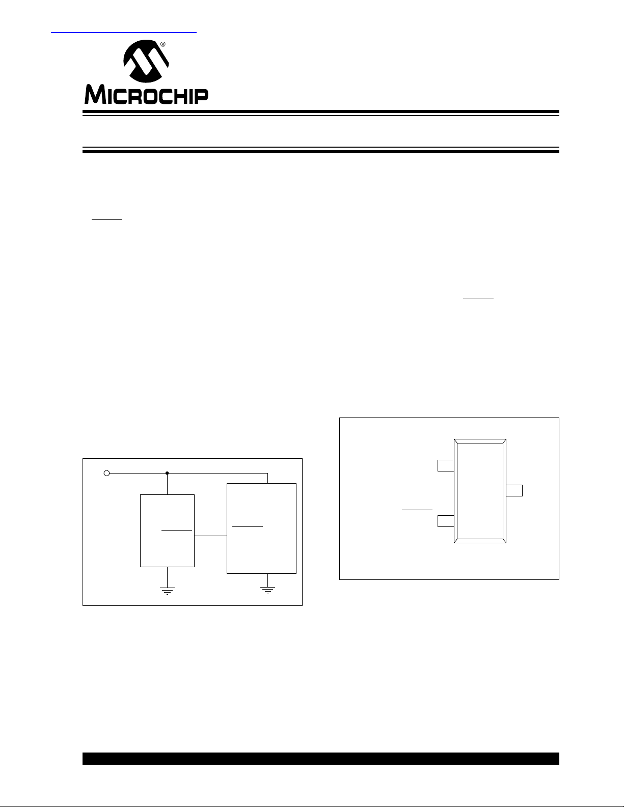
Typical Application Circuit
V
DD
3
V
DD
TCM809
RESET
GND
1
Microcontroller
2
V
DD
PICmicro
RESET
INPUT
(Active-Low)
GND
General Description
The TCM809 and TCM810 are cost-effective system
supervisor circuits designed to monitor V
systems and provide a reset signal to the host processor, when necessary. No external components are
required.
The RESET output is typically driven active within
65 µsec of V
old. RESET is maintained active for a minimum of
140 msec after VDD rises above the reset threshold.
The TCM810 has an act ive-high RESET outp ut, while
the TCM809 has an active-low RESET output. The output of the TCM809/TCM810 is valid down to V
Both devices are available in 3-Pin SC-70 and SOT-23B
packages.
The TCM809/TCM810 is optimized to reject fast
transient glitches on the V
of 9 µA (typ., V
for battery-powered applications.
falling through the reset voltage thresh-
DD
line. A low supply current
= 3.3V) make these devices suitable
DD
DD
in digital
DD
DD
= 1V.
Pin Configurations
SOT-23B/SC-70
1
GND
®
TCM809 RESET
TCM810 (RESET)
Note: 3-Pin SOT-23B is equivalent to
JEDEC TO-236.
2
TCM810
TCM809/
V
3
DD
2004 Microchip Technology Inc. DS21661C-page 1
Page 2
TCM809/TCM810
1.0 ELECTRICAL
PIN FUNCTION TABLE
CHARACTERISTICS
NAME FUNCTION
Absolute Maximum Ratings†
Supply Voltage (VDD to GND)..........................................6.0V
, RESET.................................... – 0.3V to (VDD +0.3V)
RESET
Input Current, V
Output Current, RESET
dV/dt (V
DD
Operating Temperature Range....................– 40°C to +125°C
Power Dissipation (T
3-Pin SOT-23B (derate 4 mW/°C above +70°C)......320 mW
3-Pin SC-70 (derate 2.17 mW/°C above +70°C)......174 mW
Storage Temperature Range.......................– 65°C to +150°C
Maximum Junction Temperature, T
† Notice: Stresses above those listed under “M aximum ratings” may
cause permanent damage to the device. This is a stress rating only and
functional operation of the device at those or any ot her conditions
above those indicat ed in th e o per ati o nal li st i ngs of t his specification is
not implied. Exposure to maximum rating conditions for extended periods may affect device reliability.
.........................................................20 mA
DD
, RESET...................................20 mA
).............................................................100V/µsec
= 70°C):
A
..............................150°C
J
GND Ground.
RESET
(TCM809) RESET push-pull output
remains low while V
the reset voltage threshold and
for 240 msec (140msec min.)
after V
rises above reset
DD
threshold.
RESET (TCM810) RESET push-pull output
remains high wh ile V
the reset voltage threshold and
for 240 msec (140msec min.)
after V
rises above reset
DD
threshold.
V
DD
Supply voltage (+2.5V, +3.0V,
+3.3V, +5.0V).
ELECTRICAL CHARACTERISTICS
VDD = Full Range, TA = Operating Temperature Range, unless otherwise noted. Typical values are at TA = +25°C,
= 5V for L/M/J, 3.3V for T/S, 3.0V for R and 2.5V for Z (Note 1).
V
DD
Parameter Sym Min Typ Max Units Test Conditions
Range 1.0 — 5.5 V TA = 0°C to +70°C
V
DD
1.2 — 5.5 T
Supply Current I
Reset Threshold (Note 2) V
Reset Threshold T empco — 30 — ppm/°C
V
to Reset Delay, — 65 — µsec VDD = VTH to (VTH – 100 mV) (Note 2)
DD
Reset Active Time Out
Period
Note 1: Production testing done at T
2: RESET
output for TCM809, RESET output for TCM810.
CC
TH
—1230µATCM8xxL/M/J: VDD < 5.5V
—925 TCM8xxR/S/T/Z: V
4.56 4.63 4.70 V TCM8xxL: TA = +25°C
4.50 — 4.75
4.31 4.38 4.45 V TCM8xxM: T
4.25 — 4.50 V T
3.93 4.00 4.06 V TCM809J: T
3.89 — 4.10 V T
3.04 3.08 3.11 V TCM8xxT: T
3.00 — 3.15 V T
2.89 2.93 2.96 V TCM8xxS: T
2.85 — 3.00 V T
2.59 2.63 2.66 V TCM8xxR: T
2.55 — 2.70 V T
2.28 2.32 2.35 V TCM8xxZ: T
2.25 — 2.38 V T
140 320 560 msec
= +25°C, overtemperature limits ensured by QC screen.
A
= – 40°C to +125°C
A
< 3.6V
DD
= – 40°C to +125°C
T
A
= +25°C
A
= – 40°C to +125°C
A
= +25°C
A
= – 40°C to +125°C
A
= +25°C
A
= – 40°C to +125°C
A
= +25°C
A
= – 40°C to +125°C
A
= +25°C
A
= – 40°C to +125°C
A
= +25°C
A
= – 40°C to +125°C
A
is below
DD
is below
DD
DS21661C-page 2 2004 Microchip Technology Inc.
Page 3
TCM809/TCM810
ELECTRICAL CHARACTERISTICS (CONTINUED)
VDD = Full Range, TA = Operating Temperature Range, unless otherwise noted. Typical values are at TA = +25°C,
V
= 5V for L/M/J, 3.3V for T/S, 3.0V for R and 2.5V for Z (Note 1).
DD
Parameter Sym Min Typ Max Units Test Conditions
RESET Output Voltage
Low (TCM809)
Output Voltage
RESET
High (TCM809)
RESET Output Voltage
Low (TCM810)
RESET Output Voltage
High (TCM810)
Note 1: Production testing done at T
2: RESET
output for TCM809, RESET output for TCM810.
V
OL
V
OH
V
OL
V
OH
——0.3VTCM809R/S/T/Z: VDD = VTH min, I
——0.4 TCM809L/M/J: V
——0.3 V
0.8 V
DD
V
– 1.5 — — TCM809L/M/J: VDD > VTH max, I
DD
——VTCM809R/S/T/Z: VDD > VTH max, I
> 1.0V, I
DD
SINK
DD
= 50 µA
= VTH min, I
——0.3VTCM810R/S/T/Z:VDD = VTH max, I
——0.4 TCM810L/M: V
0.8 V
DD
= +25°C, overtemperature limits ensured by QC screen.
A
——V1.8 < V
DD
< VTH min, I
= VTH max, I
DD
SOURCE
= 150 µA
SINK
SINK
SOURCE
SOURCE
SINK
= 3.2 mA
SINK
= 1.2 mA
= 3.2 mA
= 500 µA
= 800 µA
= 1.2 mA
2004 Microchip Technology Inc. DS21661C-page 3
Page 4
TCM809/TCM810
Supply Current ( µA)
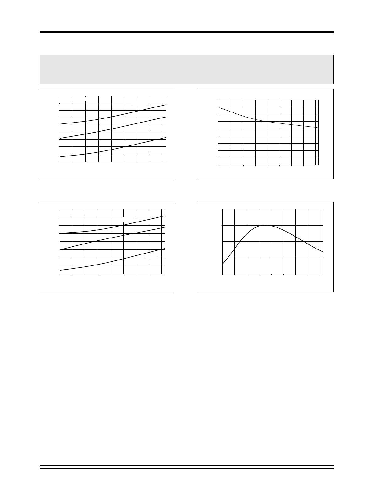
2.0 TYPICAL PERFORMANCE CHARACTERISTICS
Note: The graphs and tables provided following this note are a statistical summary based on a limited number of
samples and are provided for informational purposes only. The performance characteristics listed herein
are not tested or guaranteed. In some graphs or tables, the data presented may be outside the specified
operating range (e.g., outside specified power supply range) and therefore outside the warranted range.
18
TCM8xx/R/S/T/ Z, N o Lo ad
16
14
12
10
8
6
4
2
0
-40 -20 0 20 40 60 80 100 120
Temperature ( ° C)
VDD = 5V
VDD = 3V
VDD = 1V
450
400
350
300
250
200
150
100
Power-up Reset Timeout (µsec)
50
0
-40 -20 0 20 40 60 80 100 120
Temperature ( °C )
FIGURE 2-1: Supply Current vs.
Temperature.
16
TCM8xx/L/M/J, No Load
14
12
10
8
6
Supply Current ( µA)
4
2
0
-40-20 0 20406080100120
Temperature ( °C )
VDD = 5V
VDD = 3V
FIGURE 2-2: Supply Current vs.
Temperature.
VDD = 1V
FIGURE 2-3: Power-up Reset Time Out
vs. Temper atu re.
1.001
1
0.999
0.998
Normalized Reset Threshold
0.997
-40-200 20406080100120
Temperature (°C)
FIGURE 2-4: Normalized Reset
Threshold vs. Temperature.
DS21661C-page 4 2004 Microchip Technology Inc.
Page 5
TCM809/TCM810
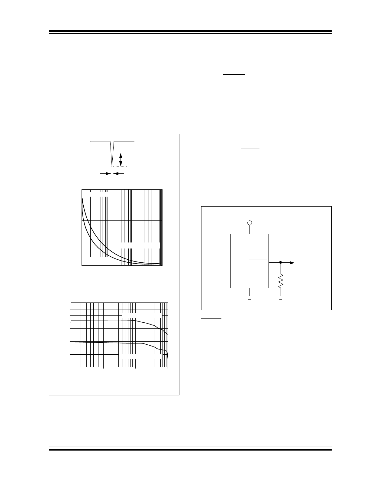
3.0 APPLICATIONS INFORMATION
3.1 VDD Transient Rejection
The TCM809/TCM8 10 prov ides accurate V
ing and reset timing during powe r-up, power-d own an d
brown-out/sag conditions. These devices also reject
negative-going transients (glitches) on the power supply line. Figure3-1 shows the maximum transient duration vs. maximum negative excursion (overdrive) for
glitch rejection. Any combination of duration and overdrive that lies under the curve will not generate a reset
signal.
V
DD
V
TH
Overdrive
Duration
400
TA = +25°C
320
240
monitor-
DD
Combinations above the curve are detected as a
brown-out or power-down condition. Transient immunity can be improved by adding a capacitor in close
proximity to the V
pin of the TCM809/TC M810.
DD
3.2 RESET Signal Integrity During
Power-Down
The TCM809 RESET output is valid to VDD = 1.0V.
Below this voltage the output becomes an "open circuit" and does not sink current. This means CMOS
logic inputs to the microcontroller will be floating at an
undetermined voltage. Most digital systems are
completely shut down well above this voltage.
However, in situations where RESET
tained valid to V
connected from RESET
= 0V, a pull-down resistor must be
DD
to ground to discharge stray
capacitance s and hold the out put low (Figure3-2). This
resistor value, though not critical, should be chosen
such that it does not appreciably load RESET
normal operation (100 kΩ will be suitable for most
applications). Similarly, a pull-up resistor to VDD is
required for the TCM810 to ensure a valid high RESET
for VDD below 1.0V.
V
DD
must be main-
under
160
80
TCM8XXZ/R/S/T
(SOT-23)
0
Maximum Transient Duration (µsec)
1
Reset Comparator Overdrive
130
120
110
100
90
80
70
60
to Reset Delay (µsec)
50
DD
40
V
30
1 10 100 1000
Reset Comparator Overdrive (mV)
TCM8XXL/M/J (SOT-23)
5
[V
TH
[VTH - VDD] (mv)
100
- VDD] (mv)
TCM8XXL/M/J (SC-70)
TCM8XXZ/R/S/T (SC-70)
1000
FIGURE 3-1: Maximum Transient
Duration vs. Overdrive for Glitch Rejection at
+25°C.
V
DD
TCM809
RESET
R
1
GND
100 kΩ
FIGURE 3-2: The addition of R1 at the
RESET
RESET
output of the TCM809 ensures that the
output is valid to V
DD
= 0V.
2004 Microchip Technology Inc. DS21661C-page 5
Page 6

TCM809/TCM810
3.3 Controllers and Processors With
Bidirectional I/O Pins
Some microcontrollers have bidirectional reset pins.
Depending on the cu rrent drive cap ability of the co ntroller pin, an indeterminate logic level may result if there
is a logic conflict. This can be avoided by adding a
4.7 kΩ resistor in series with the output of the TCM809/
TCM810 (Figure 3-3). If there are other components in
the system that require a reset signal, they should be
buffered so as not to load the reset line. If the other
components are required to follow the reset I/O of the
microcontroller, the buffer should be connected as
shown with the solid line.
Buffered RESET
To Other System
Components
®
V
DD
TCM809
RESET
GND
4.7 kΩ
Buffer
PICmicro
Micro-
controller
RESET
GND
FIGURE 3-3: Interfa cing the TCM809 to a
Bidirection al RESET I/O.
DS21661C-page 6 2004 Microchip Technology Inc.
Page 7
4.0 PACKAGING INFORMATION
4.1 Package Marking Information
3-Pin SOT-23B 3-Pin SC-70
TCM809/TCM810
cdef
cde
Top Side
Part Number SOT-23/SC-70
TCM809LENB J1
TCM809MENB J2
TCM809TENB J3
TCM809SENB J4
TCM809RENB J5
TCM809JENB J6
TCM809ZENB J7
TCM809LVNB/TCM809LVLB JZ
TCM809MVNB/TCM809MVLB JY
TCM809TVNB/TCM809TVLB JX
TCM809SVNB/TCM809SVLB JV
TCM809RVNB/TCM809RVLB JU
TCM809JVNB/TCM809JVLB JT
TCM809ZVNB/TCM809ZVLB JS (SC-70 package only)
Part Number SOT-23/SC-70
TCM810LENB K1
TCM810MENB K2
TCM810TENB K3
TCM810SENB K4
TCM810RENB K5
TCM810ZENB K6
fgh
Bottom Side
TCM810LVNB/TCM810LVLB KZ
TCM810MVNB/TCM810MVLB KY
TCM810TVNB/TCM810TVLB KX
TCM810SVNB/TCM810SVLB KV
TCM810RVNB/TCM 810RVLB KU
Legend: 1 Part Number + temperature range and voltage (two-digit code)
Note: In the event the full Microchip part number cannot be marked on one line, it will be
2004 Microchip Technology Inc. DS21661C-page 7
2 Part Number + temperature range and voltage (two-digit code)
3 Lot ID number
4 Year and work week
5 Year and work week
6 Year and work week
carried over to the next line thus limiting the number of available characters for customer
specific information.
Page 8
TCM809/TCM810
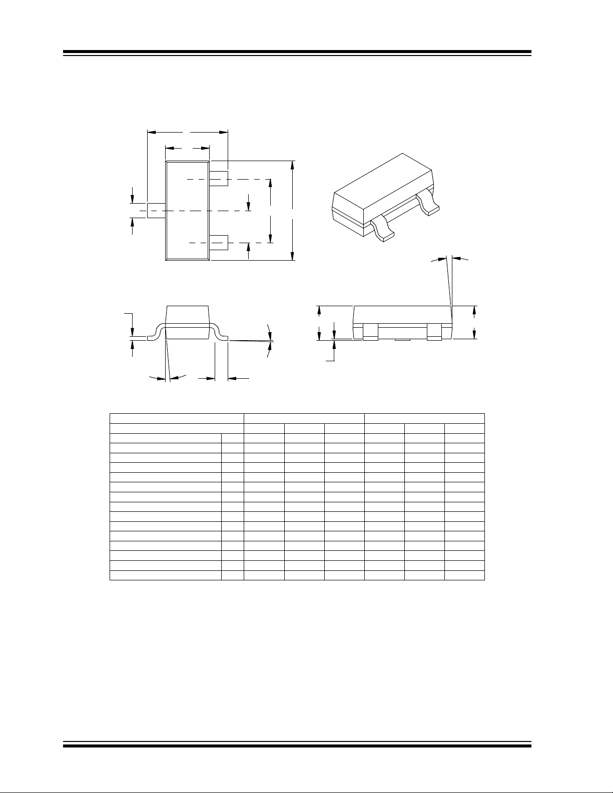
3-Lead Plastic Small Outline Transistor (NB) (SOT-23)
E
E1
2
B
n
1
c
β
Number of Pins
Pitch
Outside lead pitch (basic)
Foot Angle
Lead Thickness
Mold Draft Angle Top
Mold Draft Angle Bottom
* Controlling Parameter
§ Significant Characteristic
Notes:
Dimensions D and E1 do not include mold flash or protrusions. Mold flash or protrusions shall not exceed
.010” (0.254mm) per side.
JEDEC Equivalent: TO-236
Drawing No. C04-104
n
p
p1
φ
c
α
β
p1
D
p
A
φ
L
A1
MILLIMETERSINCHES*Units
α
A2
MAXNOMMINMAXNOMMINDimension Limits
33
0.96.038
1.92.076
1.121.010.89.044.040.035AOverall Height
1.020.950.88.040.037.035A2Molded Package Thickness
0.100.060.01.004.002.000A1Standoff §
2.642.372.10.104.093.083EOverall Width
1.401.301.20.055.051.047E1Molded Package Width
3.042.922.80.120.115.110DOverall Length
0.550.450.35.022.018.014LFoot Length
10501050
0.180.140.09.007.006.004
0.510.440.37.020.017.015BLead Width
10501050
10501050
DS21661C-page 8 2004 Microchip Technology Inc.
Page 9

3-Lead Plastic Small Outline Transistor (LB) (SC-70)
E
E1
TCM809/TCM810
B
3
2
p1 D
p
1
a
c
b
Pitch
Outside lead pitch (basic)
Lead Thickness
Mold Draft Angle Top
Mold Draft Angle Bottom
*Controlling Parameter
Notes:
Dimensions D and E1 do not include mold flash or protrusions. Mold flash or protrusions
shall not exceed .005" (0.127mm) per side.
L
p1
A
p
c
a
b
.026 BSC.
.051 BSC.
A2
A1
MILLIMETERS*INCHESUnits
MAXMINMAXMINDimension Limits
33Number of Pins
0.65 BSC.
1.30 BSC.
1.100.80.043.031AOverall Height
1.000.80.039.031A2Molded Package Thickness
.0100.00.0004.000A1Standoff
2.401.80.094.071EOverall Width
1.351.15.053.045E1Molded Package Width
2.251.80.089.071DOverall Length
0.410.10.016.004LFoot Length
0.250.08.010.003
0.400.15.016.006BLead Width
12˚8˚12˚8˚
12˚8˚12˚8˚
JEITA (EIAJ) Equivalent: SC70
Drawing No. C04-104
2004 Microchip Technology Inc. DS21661C-page 9
Page 10
TCM809/TCM810
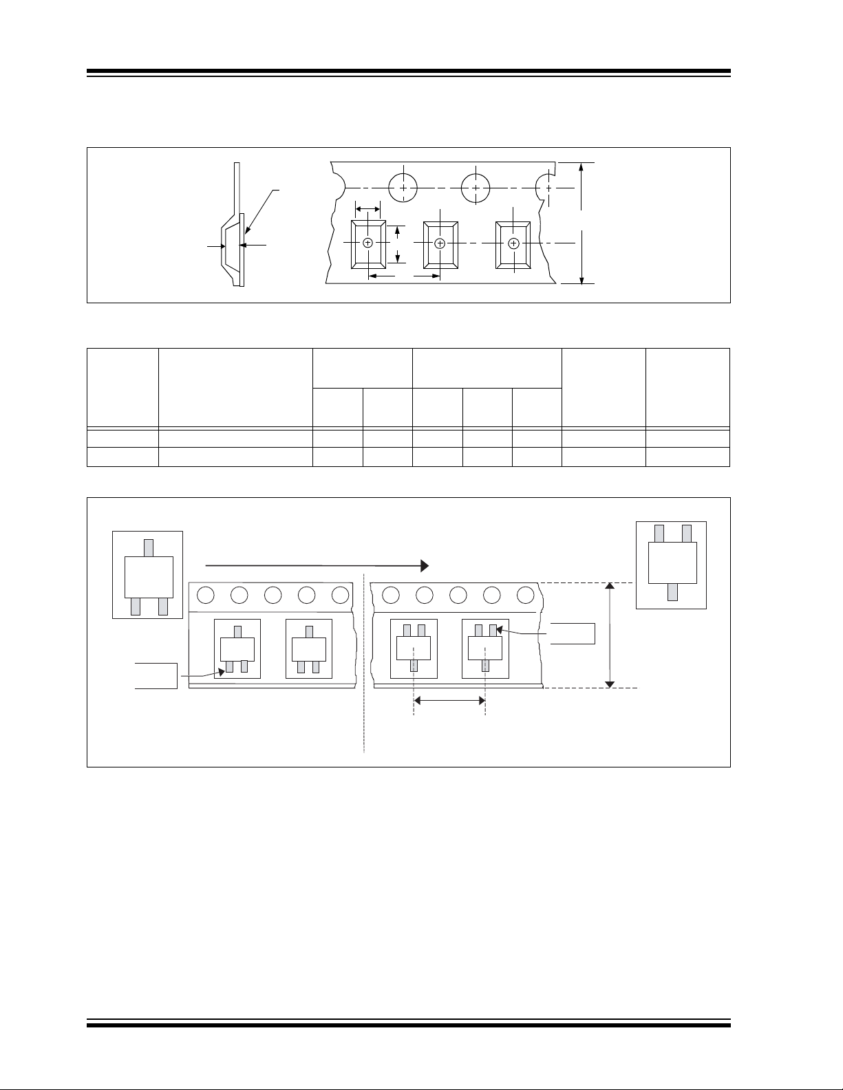
4.2 Product Tape and Reel Specifications
FIGURE 4-1: EMBOSSED CARRIER DIMENSIONS (8, 12, 16, AND 24 MM TAPE ONLY)
Top
Cover
Tape
A
0
W
K
0
B
0
P
TABLE 1: CARRIER TAPE/CAVITY DIMENSIONS
Carrier
Case
Outline
Package
Type
Dimensions
W
mm
P
mm
NB SOT-23 3L 8 4 3.15 2.77 1.22 3000 180
LB SC-70 3L 8 4 2.4 2.4 1.19 3000 180
Dimensions
A0
mm
Cavity
B0
mm
K0
mm
Output
Quantity
Units
FIGURE 4-2: 3-LEAD SOT-23/SC70 DEVICE TAPE AND REEL SPECIFICATIONS
Device
Marking
User Direction of Feed
Pin 1
W, Width
of Carrier
Reel
Diameter in
mm
Tape
Marking
Device
Pin 1
P, Pitch
Standard Reel Component Orientation
DS21661C-page 10 2004 Microchip Technology Inc.
Reverse Reel Component Orientation
Page 11

TCM809/TCM810
PRODUCT IDENTIFICATION SYSTEM
To order or obtain information, e.g., on pricing or delivery, refer to the factory or the listed sales office.
PART NO. X X
Device
V
DD
Reset
Temperature
Range
XXXX
X
Package
Threshold
Device: TCM80 9: Superv is or circuit with active-low RESET output
V
Reset Threshold: L = 4.63V
DD
Temperature Range: E = -40°C to +85°C
Package: NB713 = SOT-23B, 3-pin (Tape and Reel)
TCM810: Supervisor circuit with active-high RESET output
M=4.38V
J=4.00V
T=3.08V
S=2.93V
R=2.63V
Z=2.32V
V = -40°C to +125°C
LB713 = SC-70, 3-pin (Tape and Reel)
Examples:
a) TCM809LENB713: SOT-23B-3-TR,
b) TCM809LVLB713: SC-70-3-TR,
c) TCM809LVNB713: SOT-23B-3-TR,
a) TCM810MENB713: SOT-23B-3-TR,
b) TCM810RVLB713: SOT-23B-3-TR,
c) TCM810TVLB713: SC-70-3-TR,
Microcontroller 4.63V
Reset Monitor,
-40°C to +85°C,
Tape and Reel.
Microcontroller 4.63V
Reset Monitor,
-40°C to +125°C,
Tape and Reel.
Microcontroller 4.63V
Reset Monitor,
-40°C to +125°C,
Tape and Reel.
Microcontroller 4.38V
Reset Monitor,
-40°C to +85°C,
Tape and Reel.
Microcontroller 2.63V
Reset Monitor,
-40°C to +125°C,
Tape and Reel.
Microcontroller 4.38V
Reset Monitor,
-40°C to +125°C,
Tape and Reel.
Sales and Support
Data Sheets
Products supported by a preliminary Data Sheet may have an errata sheet describing minor operational differences and
recommended workarounds. To determine if an errata sheet exists for a particular device, please contact one of the following:
1. Your local Microc hip sales office
2. The Microchip Corporate Literature Center U.S. FAX: (480) 792-7277
3. The Microchip Worldwide Site (www.microchip.com)
Please specify which device, revision of silicon and Data Sheet (include Literature #) you are using.
Customer Notification System
Register on our web site (www.microchip.com/cn) to receive the most current information on our products.
2004 Microchip Technology Inc. DS21661C-page 11
Page 12

TCM809/TCM810
NOTES:
DS21661C-page 12 2004 Microchip Technology Inc.
Page 13

Note the following details of the code protection feature on Microchip devices:
• Microchip products meet the specification contained in their particular Microchip Data Sheet.
• Microchip believes that its family of products is one of the most secure families of its kind on the market today, when used in the
intended manner and under normal conditions.
• There are dishonest and possibly illegal methods used to breach the code protection feature. All of these methods, to our
knowledge, require using the Microchip products in a manner outside the operating specifications contained in Microchip’s Data
Sheets. Most likely, the person doing so is engaged in theft of intellectual property.
• Microchip is willing to work with the customer who is concerned about the integrity of their code.
• Neither Microchip nor any other semiconductor manufacturer can guarantee the security of their code. Code protection does not
mean that we are guaranteeing the product as “unbreakable.”
Code protection is constantly evolving. We at Microchip are com mitted to continuously improving the code protect ion f eatures of our
products. Attempts to break Microchip’s code protection feature may be a violation of the Digit al Mill ennium Copyright Act. If such acts
allow unauthorized access to your software or other copyrighted work, you may have a right to sue for relief under that Act.
Information contained in this publication regarding device
applications and the like is intended through suggestion only
and may be superseded by updates. It is your responsibility to
ensure that your application meets with your specifications.
No representation or warranty is given and no liability is
assumed by Microchip Technology Incorporated with respect
to the accuracy or use of such information, or infringement of
patents or other intellectual property rights arising from such
use or otherwise. Use of Microchip’s products as critical
components in life support systems is not authorized except
with express written approval by Microchip. No licenses are
conveyed, implicitly or otherwise, under any intellectual
property rights.
Trademarks
The Microchip name and logo, the Microchip logo, Accuron,
dsPIC, K
EELOQ, MPLAB, PIC, PICmic ro, PI C START,
PRO MATE, PowerSmart and rfPIC are registered
trademarks of Microchip Technology Incorporated in the
U.S.A. and other countries.
AmpLab, FilterLab, microID, MXDEV, M XL AB, PICMASTER,
SEEVAL, SmartShunt and The Embedded Control Solutions
Company are registered trademarks of Microchip Technology
Incorporated in the U.S.A.
Application Maestro, dsPICDEM, dsPICDEM.net,
dsPICworks, ECAN, ECONOMONITOR, FanSense,
FlexROM, fuzzyLAB, In-Circuit Serial Programming, ICSP,
ICEPIC, Migratable Memory, MPASM, MPLIB, MPLINK,
MPSIM, PICkit, PICDEM, PICDEM.net, PICtail, PowerCal,
PowerInfo, PowerMate, PowerTool, rfLAB, Select Mode,
SmartSensor, SmartTel and Total Endurance are trademarks
of Microchip Technology Incorporated in the U.S.A. and other
countries.
SQTP is a service mark of Microchip T echnology Incorporated
in the U.S.A.
All other trademarks mentioned herein are property of their
respective companies.
© 2004, Microchip Technology Incorporated, Printed in the
U.S.A., All Rights Reserved.
Printed on recycled paper.
Microchip received ISO/TS-16949:2002 quality system certification for
its worldwide headquarters, design and wafer fabrication facilities in
Chandler and Tempe, Arizona and Mountain View, California in
October 2003. The Company’s quality system processes and
procedures are for its PICmicro
devices, Serial EEPROMs, microperipherals, nonvolatile memory and
analog products. In addition, Microchip’s quality system for the design
and manufacture of development systems is ISO 9001:2000 certified.
®
8-bit MCUs, KEELOQ
®
code hopping
2004 Microchip Technology Inc. DS21661C-page 13
Page 14

WORLDWIDE SALES AND SERVICE
AMERICAS
Corporate Office
2355 West Chandler Blvd.
Chandler, AZ 85224-6199
Tel: 480-7 92- 72 00
Fax: 480-792-7277
Technical Support: 480-792-7627
Web Address: http://www.microchip.com
Atlanta
3780 Mansell Road, Suite 130
Alpharetta, GA 30022
Tel: 770 -6 40- 003 4
Fax: 770-640-0307
Boston
2 Lan Drive, Suite 120
Westford, MA 01886
Tel: 978 -6 92- 384 8
Fax: 978-692-3821
Chicago
333 Pierce Road, Suite 180
Itasca, IL 60143
Tel: 630 -2 85- 007 1
Fax: 630-285-0075
Dallas
4570 Westgrove Drive, Suite 160
Addison, TX 75001
Tel: 972 -8 18- 742 3
Fax: 972-818-2924
Detroit
Tri-Atria Office Building
32255 Northwestern Highway, Suite 190
Farmington Hills, MI 48334
Tel: 248 -5 38- 225 0
Fax: 248-538-2260
Kokomo
2767 S. Albright Road
Kokomo, IN 46902
Tel: 765 -8 64- 836 0
Fax: 765-864-8387
Los Angeles
18201 Von Karman, Suite 1090
Irvine, CA 92612
Tel: 949 -2 63- 188 8
Fax: 949-263-1338
San Jose
1300 Terra Bella Avenue
Mountain View, CA 94043
Tel: 650 -2 15- 144 4
Fax: 650-961-0286
Toronto
6285 Northam Drive, Suite 108
Mississauga, Ontario L4V 1X5, Cana da
Tel: 905 -6 73- 069 9
Fax: 905-673-6509
ASIA/PACIFIC
Australia
Suite 22, 41 Rawson Street
Epping 2121, NSW
Australia
Tel: 61- 2- 986 8-6 733
Fax: 61-2-9868-6755
China - Beijing
Unit 706B
Wan Tai Bei Hai Bldg.
No. 6 Chaoyangmen Bei Str.
Beijing, 100027, China
Tel: 86- 10 -85 282 100
Fax: 86-10-85282104
China - Chengdu
Rm. 2401-2402, 24th Floor,
Ming Xing Financial Tower
No. 88 TIDU Street
Chengdu 610016, China
Tel: 86- 28 -86 766 200
Fax: 86-28-86766599
China - Fuzhou
Unit 28F, World Trade Plaza
No. 71 Wusi Road
Fuzhou 350001, China
Tel: 86- 59 1-7 503 506
Fax: 86-591-7503521
China - Hong Kong SAR
Unit 901-6, Tower 2, Metroplaza
223 Hing Fong Road
Kwai Fong, N.T., Hong Kong
Tel: 852 -2 401 -1200
Fax: 852-2401-3431
China - Shanghai
Room 701, Bldg. B
Far East International Plaza
No. 317 Xian Xia Road
Shanghai, 200051
Tel: 86- 21 -62 75- 5700
Fax: 86-21-6275-5060
China - Shenzhen
Rm. 1812, 18/F, Building A, United Plaza
No. 5022 Binhe Road, Futian District
Shenzhen 518033, China
Tel: 86- 75 5-8 290 1380
Fax: 86-755-8295-1393
China - Shunde
Room 401, Hongjian Building, No. 2
Fengxiangnan Road, Ronggui Town, Shunde
District, Foshan City, Guangdong 528303, China
Tel: 86-757-28395507 Fax: 86-757-28395571
China - Qingdao
Rm. B505A, Fullhope Plaza,
No. 12 Hong Kong Central Rd.
Qingdao 266071, China
Tel: 86-532-5027355 Fax: 86-532-5027205
India
Divyasree Chambers
1 Floor, Wing A (A3/A4)
No. 11, O’Shaugnessey Road
Bangalore, 560 025, India
Tel: 91- 80 -22 290 06 1 Fax: 91- 80 -22 290062
Japan
Benex S-1 6F
3-18-20, Shinyokohama
Kohoku-Ku, Yokohama-shi
Kanagawa, 222-0033, Japan
Tel: 81- 45 -47 1- 6166 Fax: 81-45-471-6122
Korea
168-1, Youngbo Bldg. 3 Floor
Samsung-Dong, Kangnam-Ku
Seoul, Korea 135-882
Tel: 82-2-554-7200 Fax: 82-2-558-5932 or
82-2-558-5934
Singapore
200 Middle Road
#07-02 Prime Centre
Singapore, 188980
Tel: 65-6334-8870 Fax: 65-6334-8850
Taiwan
Kaohsiung Branch
30F - 1 No. 8
Min Chuan 2nd Road
Kaohsiung 806, Taiwan
Tel: 886-7-536-4818
Fax: 886-7-536-4803
Taiwan
Taiwan Branch
11F-3, No. 207
Tung Hua North Road
Taipei, 105, Taiwan
Tel: 886-2-2717-7175 Fax: 886-2-2545-0139
EUROPE
Austria
Durisolstrasse 2
A-4600 Wels
Austria
Tel: 43-7242-2244-399
Fax: 43-7242-2244-393
Denmark
Regus Business Centre
Lautrup hoj 1-3
Ballerup DK-2750 Denmark
Tel: 45-4420-9895 Fax: 45-4420-9910
France
Parc d’Activite du Moulin de Massy
43 Rue du Saule Trapu
Batiment A - ler Etage
91300 Massy, France
Tel: 33-1-69-53-63-20
Fax: 33-1-69-30-90-79
Germany
Steinheilstrasse 10
D-85737 Ismaning, Germany
Tel: 49-89-627-144-0
Fax: 49-89-627-144-44
Italy
Via Quasimodo, 12
20025 Legnano (MI)
Milan, Italy
Tel: 39-0331-742611
Fax: 39-0331-466781
Netherlands
P. A. De Biesbosch 14
NL-5152 SC Drunen, Netherlands
Tel: 31-416-690399
Fax: 31-416-690340
United Kingdom
505 Eskdale Road
Winnersh Triangle
Wokingham
Berkshir e, England RG41 5TU
Tel: 44-118-921-5869
Fax: 44-118-921-5820
02/17/04
DS21661C-page 14 2004 Microchip Technology Inc.
 Loading...