

TCM809/TCM810
3-Pin Microc ontroller Reset Monitors
Features
• Precision VDD Monitor for 2.5V, 3.0V, 3.3V, 5.0V
Nominal System Voltage Supplies
• 140 msec Minimum RESET Time-Out Period
• RESET Output to VDD = 1.0V (TCM809)
• Low Supply Current, 9 µA (typ.)
•VDD Transient Immunity
• Small 3-Pin SC-70 and SOT-23B Packages
• No External Components
• Push-Pull RESET Output
• Temperature Ranges:
- Industrial: SC-70 (E): -40°C to +85°C
- Extended: SOT-23, SC-70 (V): -40°C to +125°C
Applications
• Computers
• Embedded Systems
• Battery-powered Equipment
• Critical Microcontroller Power Supply Monitoring
• Automotive
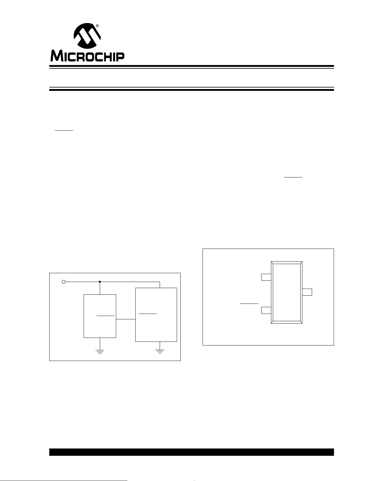
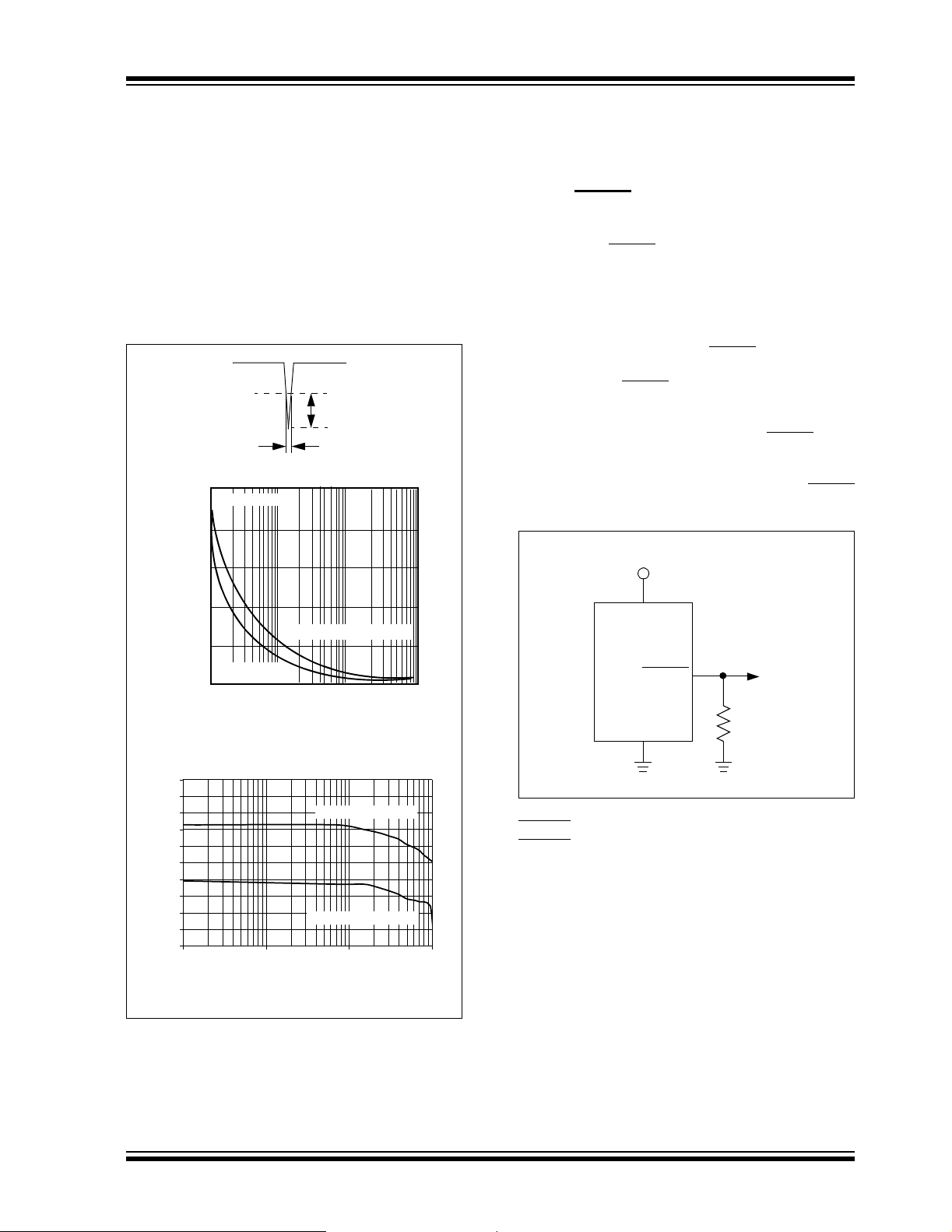
Typical Application Circuit
V
DD
3
V
DD
TCM809
RESET
GND
1
Microcontroller
2
V
DD
PICmicro
RESET
INPUT
(Active-Low)
GND
®
General Description
The TCM809 and TCM810 are cost-effective system
supervisor circuits designed to monitor V
systems; providin g a reset s ignal to th e host proc essor,
when necessary. No external components are
required.
The RESET output is typically driven active within
65 µsec of V
old. RESET is maintained active for a minimum of
140 msec after VDD rises above the reset threshold.
The TCM810 has an act ive-high RESET outp ut, while
the TCM809 has an active-low RESET output. The
output of the TCM809/TCM810 is valid down to
= 1V. Both devices are available in 3-Pin SC-70
V
DD
and SOT-23B packages.
The TCM809/TCM810 are optimized to reject fast
transient glitches on the V
of 9 µA (typ., V
for battery-powered applications.
falling through the reset voltage thresh-
DD
line. A low supply current
= 3.3V) make these devices suitable
DD
DD
in digital
DD
Pin Configurations
SOT-23B/SC-70
1
GND
V
3
DD
TCM810
TCM809 RESET
TCM810 (RESET)
Note: 3-Pin SOT -23B is equiv ale nt to
JEDEC TO-236.
2
TCM809/
© 2005 Microchip Technology Inc. DS21661D-page 1
TCM809/TCM810
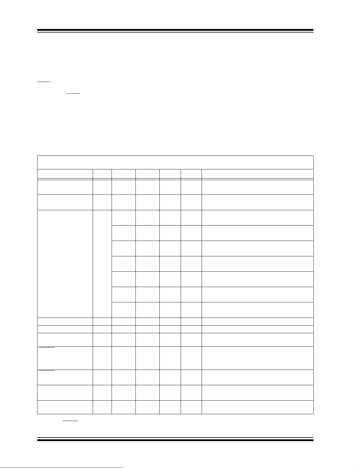
1.0 ELECTRICAL CHARACTERISTICS
† Notice: Stresses above those listed under “Maximum
Ratings” may cause permanent damage to the device. This is
a stress rating only and functional operation of the device at
those or any other conditions above those indicated in the
Absolute Maximum Ratings†
operational listings of this specification is not implied.
Exposure to maximum rating conditions fo r ext ended pe riods
Supply Voltage (VDD to GND) ........................................................6.0V
, RESET ...................................................-0.3V to (VDD +0.3V)
RESET
Input Current, V
Output Current, RESET
dV/dt (V
DD
Operating Temperature Range ...................................-40°C to +125°C
Power Dissipation (T
3-Pin SOT-23B (derate 4 mW/°C above +70°C) ....................320 mW
3-Pin SC-70 (derate 2.17 mW/°C above +70°C)....................174 mW
Storage Temperature Range.......................................-65°C to +150°C
Maximum Junction Temperature, T
.......................................................................20 mA
DD
, RESET.................................................20 mA
)...........................................................................100V/µsec
= 70°C):
A
............................................150°C
J
may affect device reliability.
ELECTRICAL CHARACTERISTICS
VDD = Full Range, TA = Operating Temperature Range, unless otherwise noted. Typical values are at TA = +25°C,
= 5V for L/M/J, 3.3V for T/S, 3.0V for R and 2.5V for Z (Note 1).
V
DD
Parameter Sym Min Typ Max Units Test Conditions
V
Range 1.0 — 5.5 V TA = 0°C to +70°C
DD
1.2 — 5.5 T
Supply Current I
CC
—1230µATCM8xxL/M/J: VDD < 5.5V
—925 TCM8xxR/S/T/Z: V
Reset Threshold (Note 2) V
TH
4.56 4.63 4.70 V TCM8xxL: TA = +25°C
4.50 — 4.75 T
4.31 4.38 4.45 V TCM8xxM: T
4.25 — 4.50 V T
3.93 4.00 4.06 V TCM809J: T
3.89 — 4.10 V T
3.04 3.08 3.11 V TCM8xxT: T
3.00 — 3.15 V T
2.89 2.93 2.96 V TCM8xxS: T
2.85 — 3.00 V T
2.59 2.63 2.66 V TCM8xxR: T
2.55 — 2.70 V T
2.28 2.32 2.35 V TCM8xxZ: T
2.25 — 2.38 V T
Reset Threshold T empco — 30 — ppm/°C
to Reset Delay, — 65 — µsec VDD = VTH to (VTH – 100 mV) (Note 2)
V
DD
Reset Active Time Out
140 320 560 msec
Period
RESET
Output Voltage
Low (TCM809)
V
OL
——0.3VTCM809R/S/T/Z: VDD = VTH min, I
——0.4 TCM809L/M/J: V
——0.3 V
RESET
Output Voltage
High (TCM809)
RESET Output Voltage
Low (TCM810)
RESET Output Voltage
High (TCM810)
Note 1: Production testing done at T
2: RESET
output for TCM809, RESET output for TCM810.
V
0.8 V
OH
V
OL
DD
– 1.5 — — TCM809L/M/J: VDD > VTH max, I
V
DD
——0.3VTCM810R/S/T/Z:VDD = VTH max, I
——VTCM809R/S/T/Z: VDD > VTH max, I
——0.4 TCM810L/M: V
0.8 V
V
OH
DD
= +25°C, overtemperature limits ensured by QC screen.
A
——V1.8 < V
= – 40°C to +125°C
A
> 1.0V, I
DD
DD
= 50 µA
SINK
DD
< VTH min, I
< 3.6V
DD
= – 40°C to +125°C
A
= +25°C
A
= – 40°C to +125°C
A
= +25°C
A
= – 40°C to +125°C
A
= +25°C
A
= – 40°C to +125°C
A
= +25°C
A
= – 40°C to +125°C
A
= +25°C
A
= – 40°C to +125°C
A
= +25°C
A
= – 40°C to +125°C
A
= VTH min, I
DD
= VTH max, I
= 150 µA
SOURCE
SINK
SINK
SOURCE
SOURCE
SINK
= 3.2 mA
SINK
= 1.2 mA
= 3.2 mA
= 500 µA
= 800 µA
= 1.2 mA
DS21661D-page 2 © 2005 Microchip Technology Inc.
TCM809/TCM810
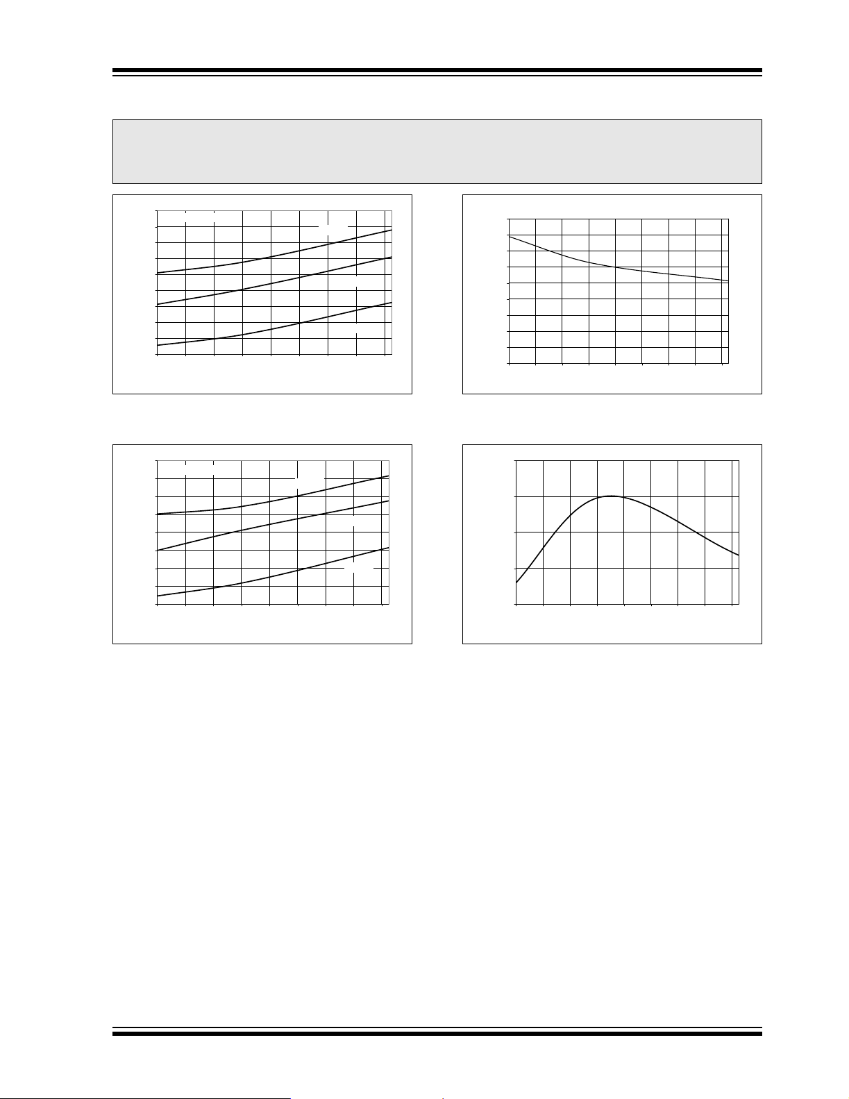
Supply Current ( µA)
2.0 TYPICAL PERFORMANCE CHARACTERISTICS
Note: The graphs and tables provided following this note are a statistical summary based on a limited number of
samples and are provided for informational purposes only. The performance characteristics listed herein
are not tested or guaranteed. In some graphs or tables, the data presented may be outside the specified
operating range (e.g., outside specified power supply range) and therefore outside the warranted range.
18
TCM8xx/R/S/T/ Z, N o Lo ad
16
14
12
10
8
6
4
2
0
-40 -20 0 20 40 60 80 100 120
Temperature ( ° C)
VDD = 5V
VDD = 3V
VDD = 1V
450
400
350
300
250
200
150
100
Power-up Reset Timeout (µsec)
50
0
-40 -20 0 20 40 60 80 100 120
Temperature ( °C )
FIGURE 2-1: Supply Current vs. Temperature.
16
TCM8xx/L/M/J, No Load
14
12
10
8
6
Supply Current ( µA)
4
2
0
-40-20 0 20406080100120
Temperature ( °C )
VDD = 5V
VDD = 3V
FIGURE 2-2: Supply Current vs. Temperature.
VDD = 1V
FIGURE 2-3: Power-up Reset Time Out vs. Temper atu re.
1.001
1
0.999
0.998
Normalized Reset Threshold
0.997
-40-200 20406080100120
Temperature (°C)
FIGURE 2-4: Normalized Reset Threshold vs. Temperature.
© 2005 Microchip Technology Inc. DS21661D-page 3
TCM809/TCM810
3.0 PIN DESCRIPTIONS
The descriptions of the pins are given in Table 3-1.
TABLE 3-1: PIN FUNCTION TABLE
NAME FUNCTION
GND Ground
RESET (TCM809) RESET push-pull output
RESET (TCM810) RESET push-pull output
V
DD
3.1 Ground (GND)
Ground terminal.
3.2 RESET Output (TCM809)
The RESET push-pull output remains low while VDD is
below the res et voltage threshold, and for 240 msec
(140 msec min.) after VDD rises above reset thres hol d.
Supply voltage (+2.5V, +3.0V,
+3.3V, +5.0V).
3.3 RESET Output (TCM810)
The RESET push-pull output remains high while VDD is
below the reset voltage threshold, and for 240 msec
(140 msec min.) after VDD rises above reset thres hol d.
3.4 Supply Voltage (VDD)
VDD: +2.5V, +3.0V, +3.3V and +5.0V
DS21661D-page 4 © 2005 Microchip Technology Inc.
TCM809/TCM810
4.0 APPLICATIONS INFORMATION
4.1 VDD Transient Rejection
The TCM809/TCM8 10 prov ides accurate V
ing and reset timing during powe r-up, power-d own an d
brown-out/sag conditions. These devices also reject
negative-going transients (glitches) on the power
supply line. Figure 4-1 shows the maximum transient
duration vs. maximum negative excursion (overdrive)
for glitch rejection. Any combination of duration and
overdrive that lies under the curve will not generate a
reset signal.
V
DD
V
TH
Overdrive
Duration
400
TA = +25°C
320
240
monitor-
DD
Combinations above the curve are detected as a
brown-out or power-down condition. Transient
immunity can be improved by adding a capacitor in
close proximity to the V
pin of the TCM809/TCM810.
DD
4.2 RESET Signal Integrity During Power-Down
The TCM809 RESET output is valid to VDD = 1.0V.
Below this voltage the output becomes an "open circuit" and does not sink current. This means CMOS
logic inputs to the microcontroller will be floating at an
undetermined voltage. Most digital systems are
completely shut down well above this voltage.
However, in situations where RESET
tained valid to V
connected from RESET
= 0V, a pull-down resistor must be
DD
to ground to discharge stray
capacitance s and hold the out put low (Figure4-2). This
resistor value, though not critical, should be chosen
such that it does not appreciably load RESET
normal operation (100 kΩ will be suitable for most
applications). Similarly, a pull-up resistor to VDD is
required for the TCM810 to ensure a valid high RESET
for VDD below 1.0V.
V
DD
must be main-
under
160
80
TCM8XXZ/R/S/T
(SOT-23)
0
Maximum Transient Duration (µsec)
1
Reset Comparator Overdrive
130
120
110
100
90
80
70
60
to Reset Delay (µsec)
50
DD
40
V
30
1 10 100 1000
Reset Comparator Overdrive (mV)
TCM8XXL/M/J (SOT-23)
5
[V
TH
[VTH – VDD] (mv)
100
– VDD] (mv)
TCM8XXL/M/J (SC-70)
TCM8XXZ/R/S/T (SC-70)
1000
FIGURE 4-1: Maximum Transient Duration vs. Overdrive for Glitch Rejection at +25°C.
V
DD
TCM809
RESET
R
1
GND
100 kΩ
FIGURE 4-2: The addition of R1 at the
RESET
RESET
output of the TCM809 ensures that the
output is valid to V
DD
= 0V.
© 2005 Microchip Technology Inc. DS21661D-page 5

TCM809/TCM810
4.3 Controllers and Processors With Bidirectional I/O Pins
Some microcontrollers have bidirectional reset pins.
Depending on the cu rrent drive cap ability of the co ntroller pin, an indeterminate logic level may result if there
is a logic conflict. This can be avoided by adding a
4.7 kΩ resistor in series with the output of the TCM809/
TCM810 (Figure 4-3). If there are other components in
the system that require a reset signal, they should be
buffered so as not to load the reset line. If the other
components are required to follow the reset I/O of the
microcontroller, the buffer should be connected as
shown with the solid line.
Buffered RESET
To Other System
Components
®
V
DD
TCM809
RESET
GND
4.7 kΩ
Buffer
PICmicro
Micro-
controller
RESET
GND
FIGURE 4-3: Interfa cing the TCM809 to a Bidirection al RESET I/O.
DS21661D-page 6 © 2005 Microchip Technology Inc.

5.0 PACKAGING INFORMATION
5.1 Package Marking Information
TCM809/TCM810
3-Pin SOT-23B
XXNN
3-Pin SC-70
XXN
Top Side
OR
XXNN
YWW
Bottom Side
Example:
Customer Specific Information Codes for:
TCM8xx
Part Number TCM809
TCM8xxLENB J1 K1
VNB JZ KZ
TCM8xxMENB J2 K2
VNB JY KY
TCM8xxTENB J3 K3
VNB JX KX
TCM8xxSENB J4 K4
VNB JV KV
TCM8xxRENB J5 K5
VNB JU KU
TCM8xxJ ENB J6 —
VNB JT KS
TCM8xxZENB J7 K6
Example:
Customer Specific Information Codes for:
TCM8xx
Part Number TCM809
TCM8xxL ELB J1 —
VLB JZ KZ
TCM8xxM ELB J2 —
VLB JY KY
TCM8xxT ELB J3 —
VLB JX KX
TCM8xxS ELB J4 —
VLB JV KV
TCM8xxR ELB J5 —
VLB JU KU
TCM8xxJ ELB J6 —
VLB JT KS
TCM8xxZ ELB J7 —
VLB JS KT
=
TCM810
=
TCM810
Legend: XX...X Customer-specific information*
Y Year code (last digit of calendar year)
YY Year code (last 2 digits of calendar year)
WW Week code (week of January 1 is week ‘01’)
NNN Alphanumeric traceability code
3
e
Pb-free JEDEC designator for Matte Tin (Sn)
* This package is Pb-fr ee. The Pb-free JEDEC designator ( )
can be found on the outer packaging for this package.
Note: In the even t the full M icroc hip p art numb er cann ot be mark ed on one line, it wil l
be carried over to the next line, thus limiting the number of available
characters for customer-specific information.
© 2005 Microchip Technology Inc. DS21661D-page 7
3
e

TCM809/TCM810
3-Lead Plastic Small Outline Transistor (NB) (SOT-23)
E
E1
2
B
n
1
c
β
Number of Pins
Pitch
Outside lead pitch (basic)
Foot Angle
Lead Thickness
Mold Draft Angle Top
Mold Draft Angle Bottom
* Controlling Parameter
§ Significant Characteristic
Notes:
Dimensions D and E1 do not include mold flash or protrusions. Mold flash or protrusions shall not exceed
.010” (0.254mm) per side.
JEDEC Equivalent: TO-236
Drawing No. C04-104
n
p
p1
φ
c
α
β
p1
D
p
A
φ
L
A1
MILLIMETERSINCHES*Units
.038
α
A2
MAXNOMMINMAXNOMMINDimension Limits
33
0.96
1.92.076
1.121.010.89.044.040.035AOverall Height
1.020.950.88.040.037.035A2Molded Package Thickness
0.100.060.01.004.002.000A1Standoff §
2.642.372.10.104.093.083EOverall Width
1.401.301.20.055.051.047E1Molded Package Width
3.042.922.80.120.115.110DOverall Length
0.550.450.35.022.018.014LFoot Length
10501050
0.180.140.09.007.006.004
0.510.440.37.020.017.015BLead Width
10501050
10501050
DS21661D-page 8 © 2005 Microchip Technology Inc.

3-Lead Plastic Small Outline Transistor (LB) (SC-70)
E
E1
TCM809/TCM810
B
3
2
p1 D
p
1
a
c
b
Pitch
Outside lead pitch (basic)
Lead Thickness
Mold Draft Angle Top
Mold Draft Angle Bottom
*Controlling Parameter
Notes:
Dimensions D and E1 do not include mold flash or protrusions. Mold flash or protrusions
shall not exceed .005" (0.127mm) per side.
L
p
p1
c
a
b
A
.026 BSC.
.051 BSC.
A2
A1
MILLIMETERS*INCHESUnits
MAXMINMAXMINDimension Limits
33Number of Pins
0.65 BSC.
1.30 BSC.
1.100.80.043.031AOverall Height
1.000.80.039.031A2Molded Package Thickness
.0100.00.0004.000A1Standoff
2.401.80.094.071EOverall Width
1.351.15.053.045E1Molded Package Width
2.251.80.089.071DOverall Length
0.410.10.016.004LFoot Length
0.250.08.010.003
0.400.15.016.006BLead Width
12°8°12°8°
12°8°12°8°
JEITA (EIAJ) Equivalent: SC70
Drawing No. C04-104
© 2005 Microchip Technology Inc. DS21661D-page 9

TCM809/TCM810
5.2 Product Tape and Reel Specifications
FIGURE 5-1: EMBOSSED CARRIER DIMENSIONS (8, 12, 16 AND 24 MM TAPE ONLY)
Top
Cover
Tape
A
0
W
K
0
B
0
P
TABLE 1: CARRIER TAPE/CAVITY DIMENSIONS
Carrier
Case
Outline
Package
Type
Dimensions
W
mmPmm
mm
NB SOT-23 3L 8 4 3.15 2.77 1.22 3000 180
LB SC-70 3L 8 4 2.4 2.4 1.19 3000 180
Dimensions
A0
Cavity
B0
mm
K0
mm
Output
Quantity
Units
FIGURE 5-2: 3-LEAD SOT-23/SC70 DEVICE TAPE AND REEL SPECIFICATIONS
Device
Marking
User Direction of Feed
Pin 1
W, Width
of Carrier
Reel
Diameter in
mm
Marking
Device
Tape
Pin 1
P, Pitch
Standard Reel Component Orientation
DS21661D-page 10 © 2005 Microchip Technology Inc.
Reverse Reel Component Orientation

APPENDIX A: REVISION HISTORY
Revision D (March 2005)
• Updated 6.0 “Packaging Information” to include
old and new packaging examples.
• Applied new template and rearranged sections to
be consistent with current documentat ion.
Revision C (April 2004)
Revision B (January 2002)
Revision A (May 2001)
Initial release of data sheet.
TCM809/TCM810
© 2005 Microchip Technology Inc. DS21661D- page 11

TCM809/TCM810
NOTES:
DS21661D-page 12 © 2005 Microchip Technology Inc.

TCM809/TCM810
PRODUCT IDENTIFICATION SYSTEM
To order or obtain information, e.g., on pricing or delivery, refer to the factory or the listed sales office.
PART NO. X X
Device
V
DD
Reset
Temperature
Range
XXXXX
Package
Threshold
Device: TCM80 9: Superv is or circuit with active-low RESET output
V
Reset Threshold: L = 4.63V
DD
Temperature Range: E = -40°C to +85°C
Package: NB713 = SOT-23B, 3-pin (Tape and Reel)
TCM810: Supervisor circuit with active-high RESET output
M=4.38V
J=4.00V
T=3.08V
S=2.93V
R=2.63V
Z=2.32V
V = -40°C to +125°C
LB713 = SC-70, 3-pin (Tape and Reel)
Examples:
a) TCM809LENB713: SOT-23B-3-TR,
b) TCM809LVLB713: SC-70-3-TR,
c) TCM809LVNB713: SOT-23B-3-TR,
a) TCM810MENB713: SOT-23B-3-TR,
b) TCM810RVLB713: SOT-23B-3-TR,
c) TCM810TVLB713: SC-70-3-TR,
Microcontroller 4.63V
Reset Monitor,
-40°C to +85°C,
Tape and Reel.
Microcontroller 4.63V
Reset Monitor,
-40°C to +125°C,
Tape and Reel.
Microcontroller 4.63V
Reset Monitor,
-40°C to +125°C,
Tape and Reel.
Microcontroller 4.38V
Reset Monitor,
-40°C to +85°C,
Tape and Reel.
Microcontroller 2.63V
Reset Monitor,
-40°C to +125°C,
Tape and Reel.
Microcontroller 4.38V
Reset Monitor,
-40°C to +125°C,
Tape and Reel.
Sales and Support
Data Sheets
Products supported by a preliminary Data Sheet may have an errata sheet describing minor operational differences and
recommended workarounds. To determine if an errata sheet exists for a particular device, please contact one of the following:
1. Your local Microc hip sales office
2. The Microchip Corporate Literature Center U.S. FAX: (480) 792-7277
3. The Microchip Worldwide Site (www.microchip.com)
Please specify which device, revision of silicon and Data Sheet (include Literature #) you are using.
Customer Notification System
Register on our web site (www.microchip.com) to receive the most current information on our products .
© 2005 Microchip Technology Inc. DS21661D-page 13

TCM809/TCM810
NOTES:
DS21661D-page 14 © 2005 Microchip Technology Inc.

Note the following details of the code protection feature on Microchip devices:
• Microchip products meet the specification contained in their particular Microchip Data Sheet.
• Microchip believes that its family of products is one of the most secure families of its kind on the market today, when used in the
intended manner and under normal conditions.
• There are dishonest and possibly illegal methods used to breach the code protection feature. All of these methods, to our
knowledge, require using the Microchip products in a manner outside the operating specifications contained in Microchip’s Data
Sheets. Most likely, the person doing so is engaged in theft of intellectual property.
• Microchip is willing to work with the customer who is concerned about the integrity of their code.
• Neither Microchip nor any other semiconductor manufacturer can guarantee the security of their code. Code protection does not
mean that we are guaranteeing the product as “unbreakable.”
Code protection is constantly evolving. We at Microchip are com mitted to continuously improving the code protect ion f eatures of our
products. Attempts to break Microchip’s code protection feature may be a violation of the Digit al Mill ennium Copyright Act. If such acts
allow unauthorized access to your software or other copyrighted work, you may have a right to sue for relief under that Act.
Information contained in this publication regarding device
applications and the like is provided only for your convenience
and may be superseded by updates. It is your responsibility to
ensure that your application meets with your specifications.
MICROCHIP MAKES NO REPRESENTATIONS OR WARRANTIES OF ANY KIND WHETHER EXPRESS OR IMPLIED,
WRITTEN OR ORAL, STATUTORY OR OTHERWISE,
RELATED TO THE INFORMATION, INCLUDING BUT NOT
LIMITED TO ITS CONDITION, QUALITY, PERFORMANCE,
MERCHANTABILITY OR FITNESS FOR PURPOSE.
Microchip disclaims all liability arising from this information and
its use. Use of M icrochip’s prod ucts as critical components in
life support systems is not authorized except with express
written approval by Microchip. No licenses are conveyed,
implicitly or otherwise, under any Microchip intellectual property
rights.
Trademarks
The Microchip name and logo, the Microchip logo, Accuron,
dsPIC, K
EELOQ, microID, MPLAB, PIC, PICmicro, PICSTART,
PRO MATE, PowerSmart, rfPIC, and SmartShunt are
registered trademarks of Microchip Technology Incorporated
in the U.S.A. and other countries.
AmpLab, FilterLab, Migratable Memory, MXDEV, MXLAB,
PICMASTER, SEEVAL, SmartSensor and The Embedded
Control Solutions Company are registered trademarks of
Microchip Technology Incorporated in the U.S.A.
Analog-for-the-Digital Age, Application Maestro, dsPICDEM,
dsPICDEM.net, dsPICworks, ECAN, ECONOMONITOR,
FanSense, FlexROM, fuzzyLAB, In-Circuit Serial
Programmin g, IC SP, ICEPI C , MPASM, MPLI B, MP L I N K,
MPSIM, PICkit, PICDEM, PICDEM.net, PICLAB, PICtail,
PowerCal, PowerInfo, PowerMate, PowerTool, rfLAB,
rfPICDEM, Select Mode, Smart Serial, SmartTel, Total
Endurance and WiperLock are trademarks of Microchip
Technology Incorporated in the U.S.A. and other countries.
SQTP is a service mark of Microchip T echnology Incorporated
in the U.S.A.
All other trademarks mentioned herein are property of their
respective companies.
© 2005, Microchip Technology Incorporated, Printed in the
U.S.A., All Rights Reserved.
Printed on recycled paper.
Microchip received ISO/TS-16949:2002 quality system certification for
its worldwide headquarters, design and wafer fabrication facilities in
Chandler and Tempe, Arizona and Mountain View, California in
October 2003. The Company’s quality system processes and
procedures are for its PICmicro
devices, Serial EEPROMs, microperipherals, nonvolatile memory and
analog products. In addition, Microchip’s quality system for the design
and manufacture of development systems is ISO 9001:2000 certified.
®
8-bit MCUs, KEELOQ
®
code hopping
© 2005 Microchip Technology Inc. DS21661D-page 15

WORLDWIDE SALES AND SERVICE
AMERICAS
Corporate Office
2355 West Chandler Blvd.
Chandler, AZ 85224-6199
Tel: 480-792-7200
Fax: 480-792-7277
Technical Support:
http://support.microchip.com
Web Address:
www.microchip.com
Atlanta
Alpharetta, GA
Tel: 770-640-0034
Fax: 770-640-0307
Boston
Westborough, MA
Tel: 774-760-0087
Fax: 774-760-0088
Chicago
Itasca, IL
Tel: 630-285-0071
Fax: 630-285-0075
Dallas
Addison, TX
Tel: 972-818-7423
Fax: 972-818-2924
Detroit
Farmington Hills, MI
Tel: 248-538-2250
Fax: 248-538-2260
Kokomo
Kokomo, IN
Tel: 765-864-8360
Fax: 765-864-8387
Los Angeles
Mission Viejo, CA
Tel: 949-462-9523
Fax: 949-462-9608
San Jose
Mountain View, CA
Tel: 650-215-1444
Fax: 650-961-0286
Toronto
Mississauga, Ontario,
Canada
Tel: 905-673-0699
Fax: 905-673-6509
ASIA/PACIFIC
Australia - Sydney
Tel: 61-2-9868-6733
Fax: 61-2-9868-6755
China - Beijing
Tel: 86-10-8528-2100
Fax: 86-10-8528-2104
China - Chengdu
Tel: 86-28-8676-6200
Fax: 86-28-8676-6599
China - Fuzhou
Tel: 86-591-8750-3506
Fax: 86-591-8750-3521
China - Hong Kong SAR
Tel: 852-2401-1200
Fax: 852-2401-3431
China - Shanghai
Tel: 86-21-5407-5533
Fax: 86-21-5407-5066
China - Shenyang
Tel: 86-24-2334-2829
Fax: 86-24-2334-2393
China - Shenzhen
Tel: 86-755-8203-2660
Fax: 86-755-8203-1760
China - Shunde
Tel: 86-757-2839-5507
Fax: 86-757-2839-5571
China - Qingdao
Tel: 86-532-502-7355
Fax: 86-532-502-7205
ASIA/PACIFIC
India - Bangalore
Tel: 91-80-2229-0061
Fax: 91-80-2229-0062
India - New Delhi
Tel: 91-11-5160-8631
Fax: 91-11-5160-8632
Japan - Kanagawa
Tel: 81-45-471- 6166
Fax: 81-45-471-6122
Korea - Seoul
Tel: 82-2-554-7200
Fax: 82-2-558-5932 or
82-2-558-5934
Singapore
Tel: 65-6334-8870
Fax: 65-6334-8850
Taiwan - Kaohsiung
Tel: 886-7-536-4818
Fax: 886-7-536-4803
Taiwan - Taipei
Tel: 886-2-2500-6610
Fax: 886-2-2508-0102
Taiwan - Hsinchu
Tel: 886-3-572-9526
Fax: 886-3-572-6459
EUROPE
Austria - Weis
Tel: 43-7242-2244-399
Fax: 43-7242-2244-393
Denmark - Ballerup
Tel: 45-4450-2828
Fax: 45-4485-2829
France - Massy
Tel: 33-1-69-53-63-20
Fax: 33-1-69-30-90-79
Germany - Ismaning
Tel: 49-89-627-144-0
Fax: 49-89-627-144-44
Italy - Milan
Tel: 39-0331-742611
Fax: 39-0331-466781
Netherlands - Drunen
Tel: 31-416-690399
Fax: 31-416-690340
England - Berkshire
Tel: 44-118-921-5869
Fax: 44-118-921-5820
03/01/05
DS21661D-page 16 © 2005 Microchip Technology Inc.
 Loading...