

TC9400/9401/9402
1
2
3
4
5
6
7
14
13
12
11
10
9
8
V
DD
NC
AMPLIFIER OUT
THRESHOLD
DETECTOR
FREQ/2 OUT
OUTPUT COMMON
PULSE FREQ OUT
I
BIAS
ZERO ADJ
I
IN
V
SS
V
REF
OUT
GND
V
REF
1
2
3
4
5
6
7
14
13
12
11
10
9
8
TC9400
TC9401
TC9402
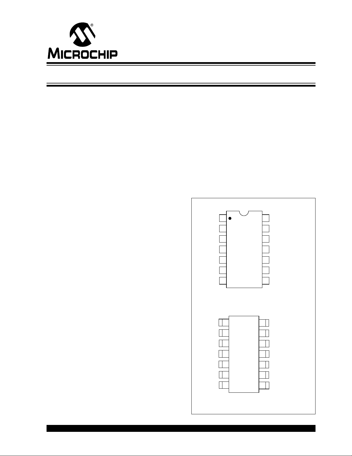
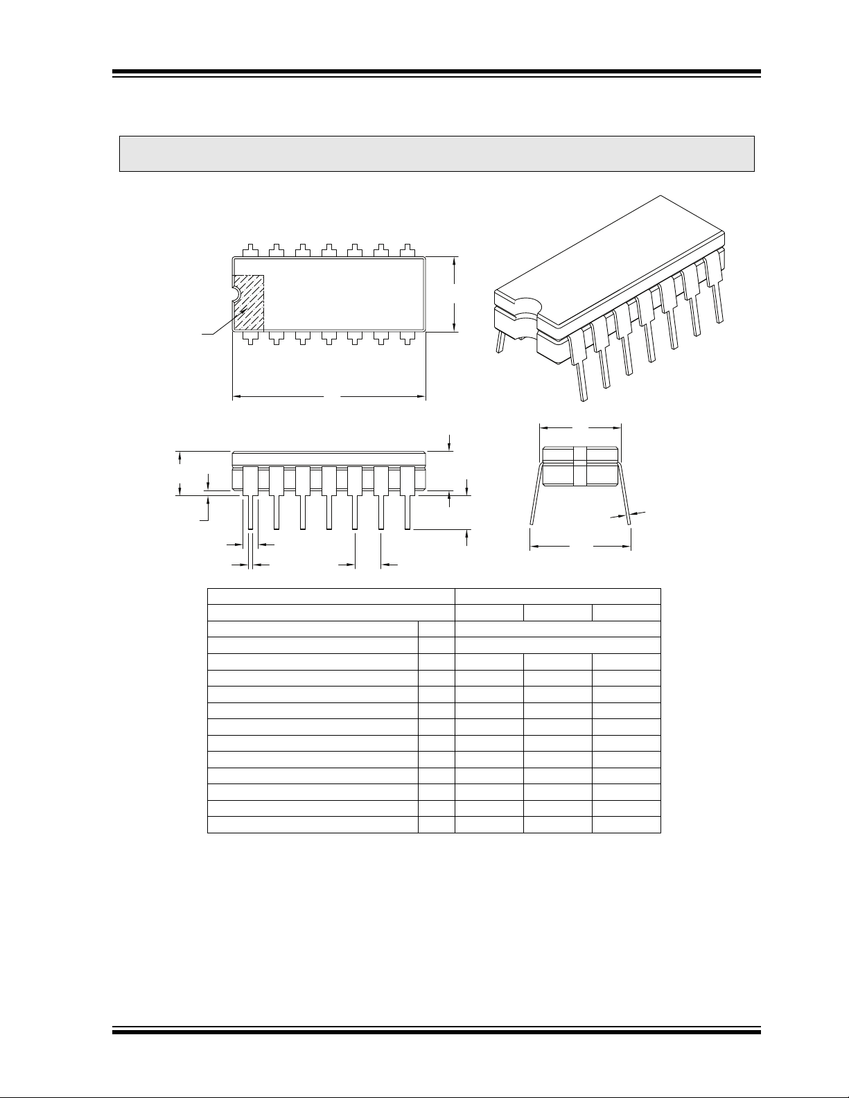
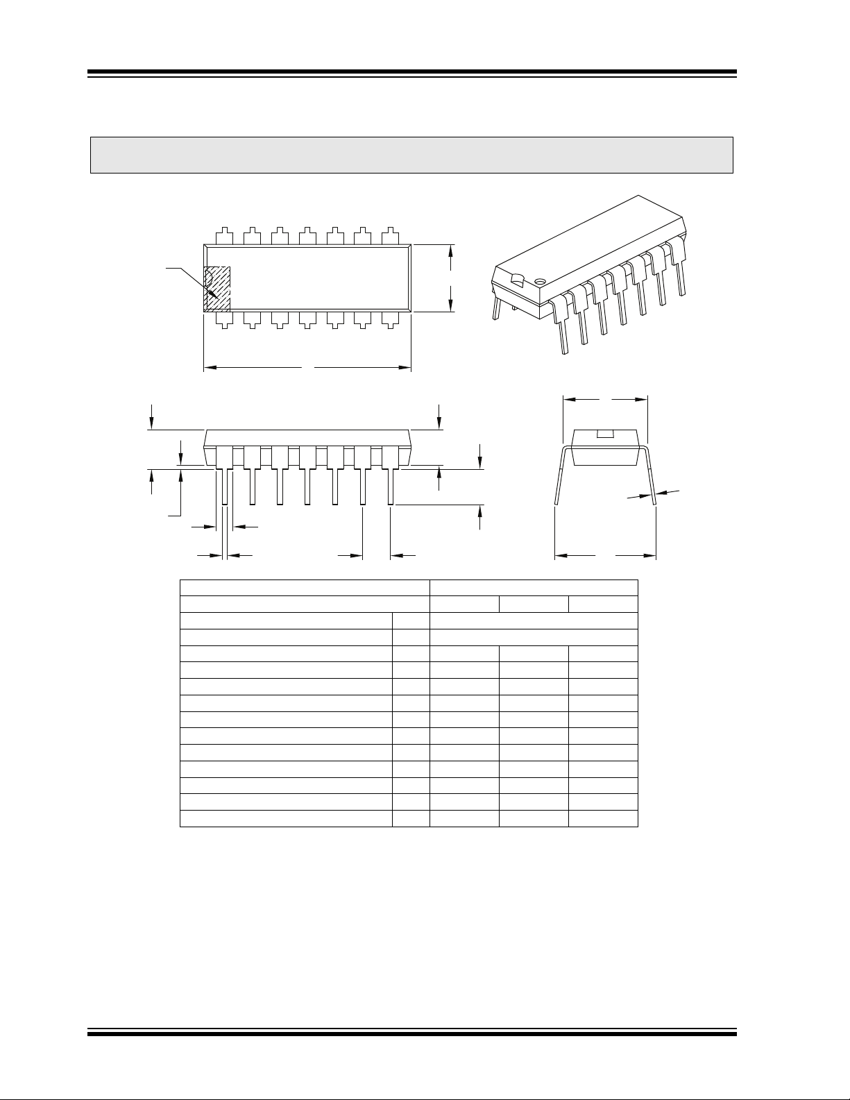
14-Pin Plastic DIP/CERDIP
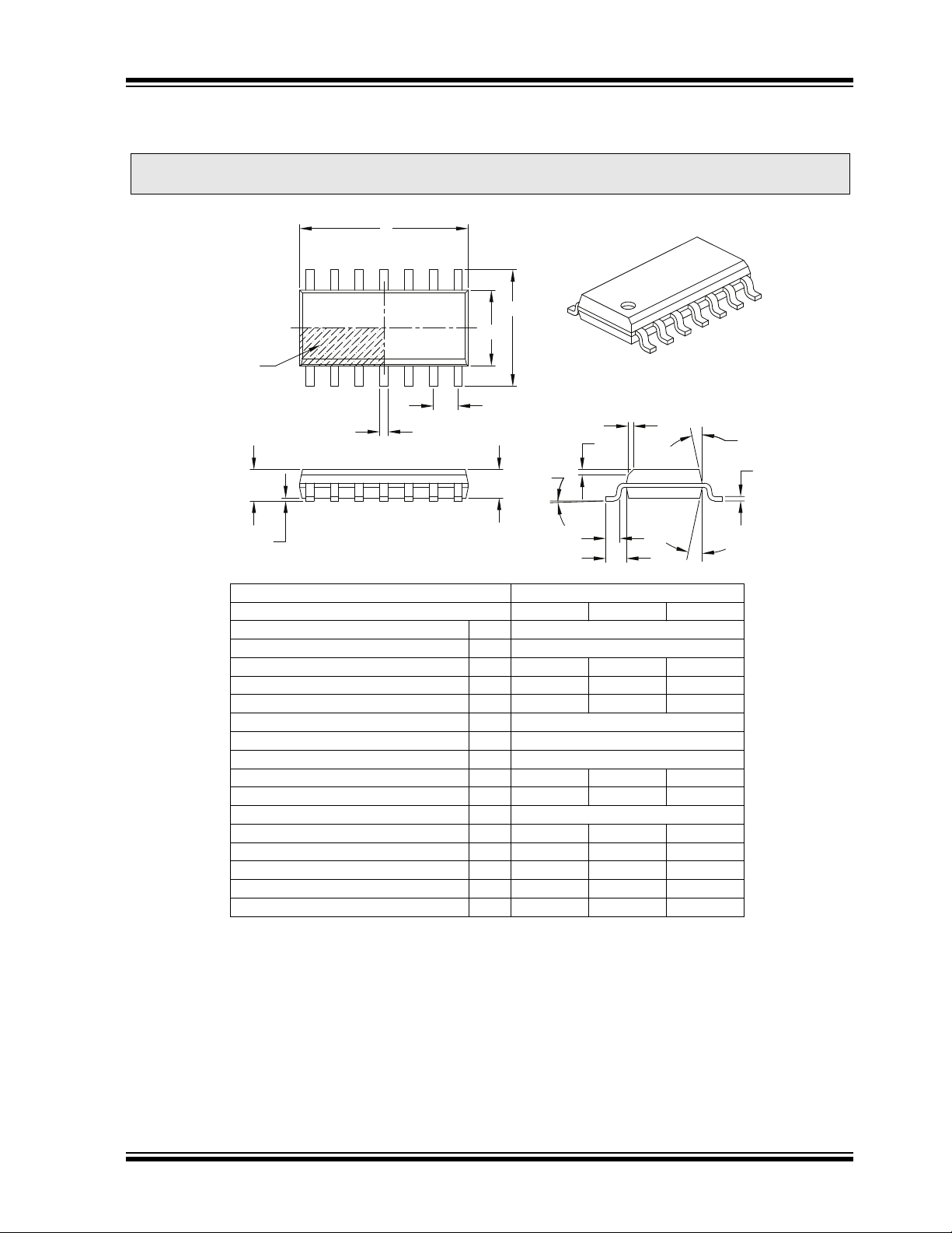
14-Pin SOIC
TC9400
TC9401
TC9402
NC = No Internal Connection
V
DD
NC
AMPLIFIER OUT
THRESHOLD
DETECTOR
FREQ/2 OUT
OUTPUT COMMON
PULSE FREQ OUT
I
BIAS
ZERO ADJ
I
IN
V
SS
V
REF
OUT
GND
V
REF
Voltage-to-Frequency / Frequency-to-Voltage Converters
Features:
VOLTAGE-TO-FREQUENCY
• Choice of Linearity:
- TC9401: 0.01%
- TC9400: 0.05%
- TC9402: 0.25%
• DC to 100 kHz (F/V) or 1 Hz to 100 kHz (V/F)
• Low Power Dissipation: 27 mW (Typ.)
• Single/Dual Supply Operation:
- +8V to +15V or ±4V to ±7.5V
• Gain Temperature Stability: ±25 ppm/°C (Typ.)
• Programmable Scale Factor
FREQUENCY-TO-VOLTAGE
• Operation: DC to 100 kHz
• Choice of Linearity:
- TC9401: 0.02%
- TC9400: 0.05%
- TC9402: 0.25%
• Programmable Scale Factor
Applications:
• Microprocessor Data Acquisition
• 13-bit Analog-to-Digital Converters (ADC)
• Analog Data Transmission and Recording
• Phase Locked Loops
• Frequency Meters/Tachometer
• Motor Control
• FM Demodulation
General Description:
The TC9400/9401/9402 are low-cost Voltage-to-Frequency (V/F) converters, utilizing low-power CMOS
technology. The converters accept a variable analog
input signal and generate an output pulse train, whose
frequency is linearly proportional to the input voltage.
The devices can also be used as highly accurate
Frequency-to-Voltage (F/V) converters, accepting
virtually any input frequency waveform and providing a
linearly proportional voltage output.
A complete V/F or F/V system only requires the
addition of two capacitors, three resistors, and reference voltage.
Package Type
© 2007 Microchip Technology Inc. DS21483D-page 1
TC9400/9401/9402
I
IN
I
REF
TC9400
R
IN
Integrator
Op Amp
Integrator
Capacitor
Threshold
Detector
One
Shot
Pulse Output
Pulse/2 Output
÷2
Input
Voltage
Reference
Capacitor
Reference
Voltage
Functional Block Diagram
DS21483D-page 2 © 2007 Microchip Technology Inc.
TC9400/9401/9402
1.0 ELECTRICAL CHARACTERISTICS
Absolute Maximum Ratings †
VDD – VSS ......................................................................+18V
..................................................................................10 mA
I
IN
– V
V
OUTMAX
– VSS .....................................................................-1.5V
V
REF
Storage Temperature Range .........................-65°C to +150°C
Operating Temperature Range:
C Device ...................................................... 0°C to +70°C
E Device.................................................... -40°C to +85°C
Package Dissipation (T
8-Pin CerDIP........................................................800 mW
8-Pin Plastic DIP ..................................................730 mW
8-Pin SOIC...........................................................470 mW
Common.................................................23V
OUT
≤ 70°C):
A
† Stresses above those listed under “Absolute Maximum
Ratings” may cause permanent damage to the device. These
are stress ratings only and functional operation of the device
at these or any other conditions above those indicated in the
operation sections of the specifications is not implied.
Exposure to Absolute Maximum Rating conditions for
extended periods may affect device reliability.
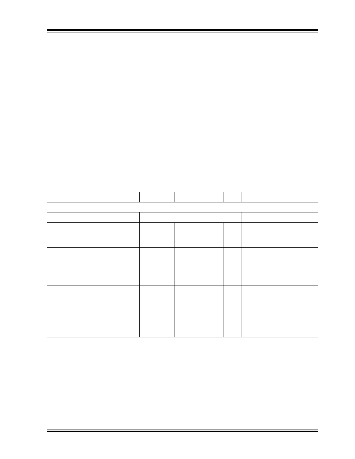
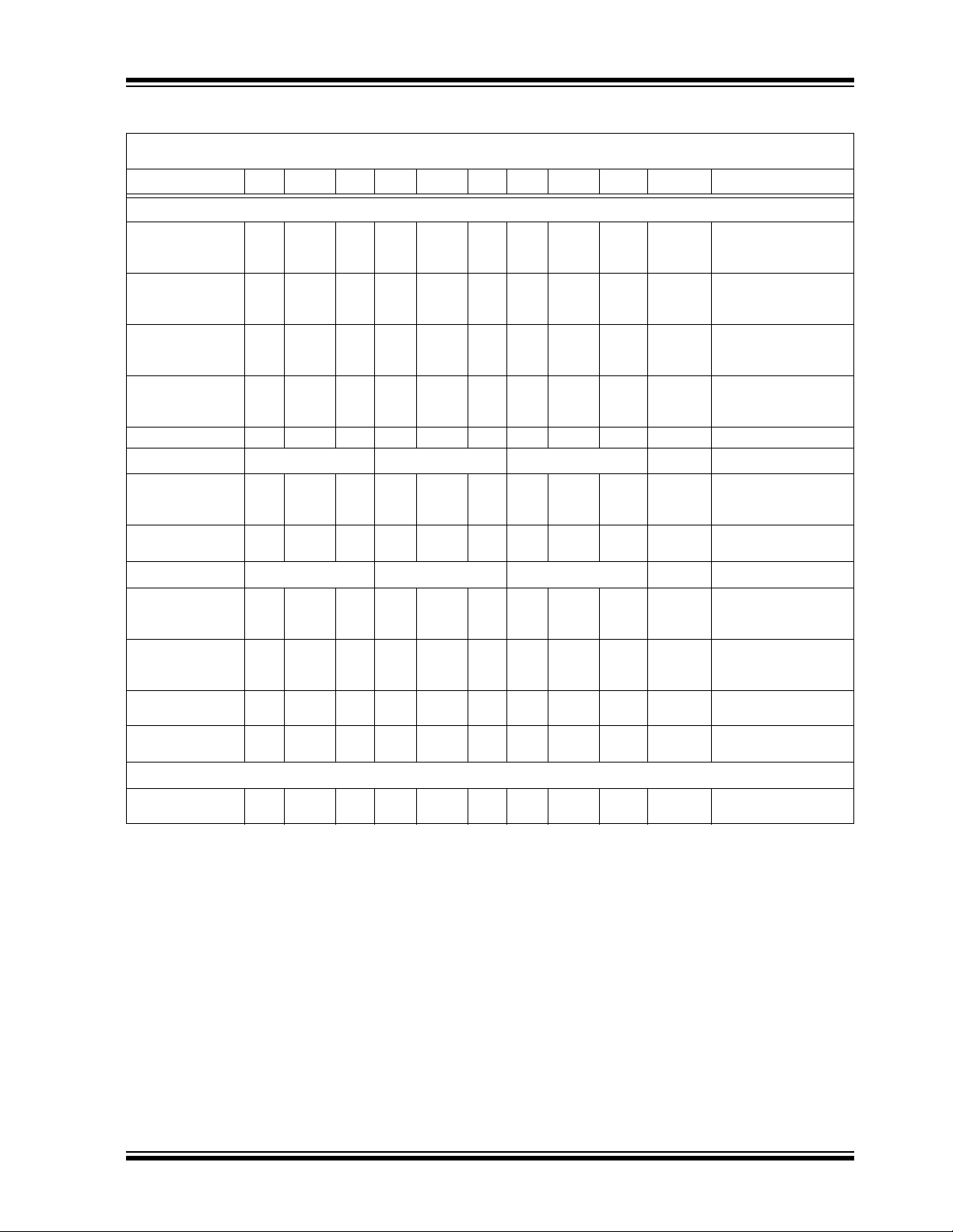
TC940X ELECTRICAL SPECIFICATIONS
Electrical Characteristics: unless otherwise specified, VDD = +5V, VSS = -5V, V
10 kHz. T
= +25°C, unless temperature range is specified (-40°C to +85°C for E device, 0°C to +70°C for C device).
A
Parameter Min Typ Max Min Typ Max Min Typ Max Units Test Conditions
Voltage-to-Frequency
GND
= 0V, V
REF
= -5V, R
= 100 kΩ, Full Scale =
BIAS
Accuracy TC9400 TC9401 TC9402
Linearity 10 kHz — 0.01 0.05 — 0.004 0.01 — 0.05 0.25 %
Linearity 100 kHz — 0.1 0.25 — 0.04 0.08 — 0.25 0.5 %
Gain Temperature
Drift (Note 1)
Gain Variance — ±10 — — ±10 — — ±10 — % of
Zero Offset
(Note 2)
Zero Temperature
Drift (Note 1)
Note 1: Full temperature range; not tested.
2: I
= 0.
IN
3: Full temperature range, I
4: I
OUT
5: Threshold Detect = 5V, Amp Out = 0V, full temperature range.
6: 10 Hz to 100 kHz; not tested.
7: 5 µs minimum positive pulse width and 0.5 µs minimum negative pulse width.
8: t
= tF = 20 ns.
R
9: R
≥ 2kΩ, tested @ 10 kΩ.
L
10: Full temperature range, V
— ±25 ±40 — ±25 ±40 — ±50 ± 100 ppm/°C
— ±10 ±50 — ±10 ±50 — ±20 ±100 mV Correction at Zero
— ±25 ±50 — ±25 ±50 — ±50 ±100 µV/°C Variation in Zero Offset
= 10 mA.
= 10 µA.
OUT
= -0.1V.
IN
Full Scale
Full Scale
Full Scale
Nominal
Output Deviation from
Straight Line Between
Normalized Zero and
Full Scale Input
Output Deviation from
Straight Line Between
Normalized Zero Reading and Full Scale Input
Variation in Gain A due
to Temperature Change
Variation from Ideal
Accuracy
Adjust for Zero Output
when Input is Zero
Due to Temperature
Change
© 2007 Microchip Technology Inc. DS21483D-page 3
TC9400/9401/9402
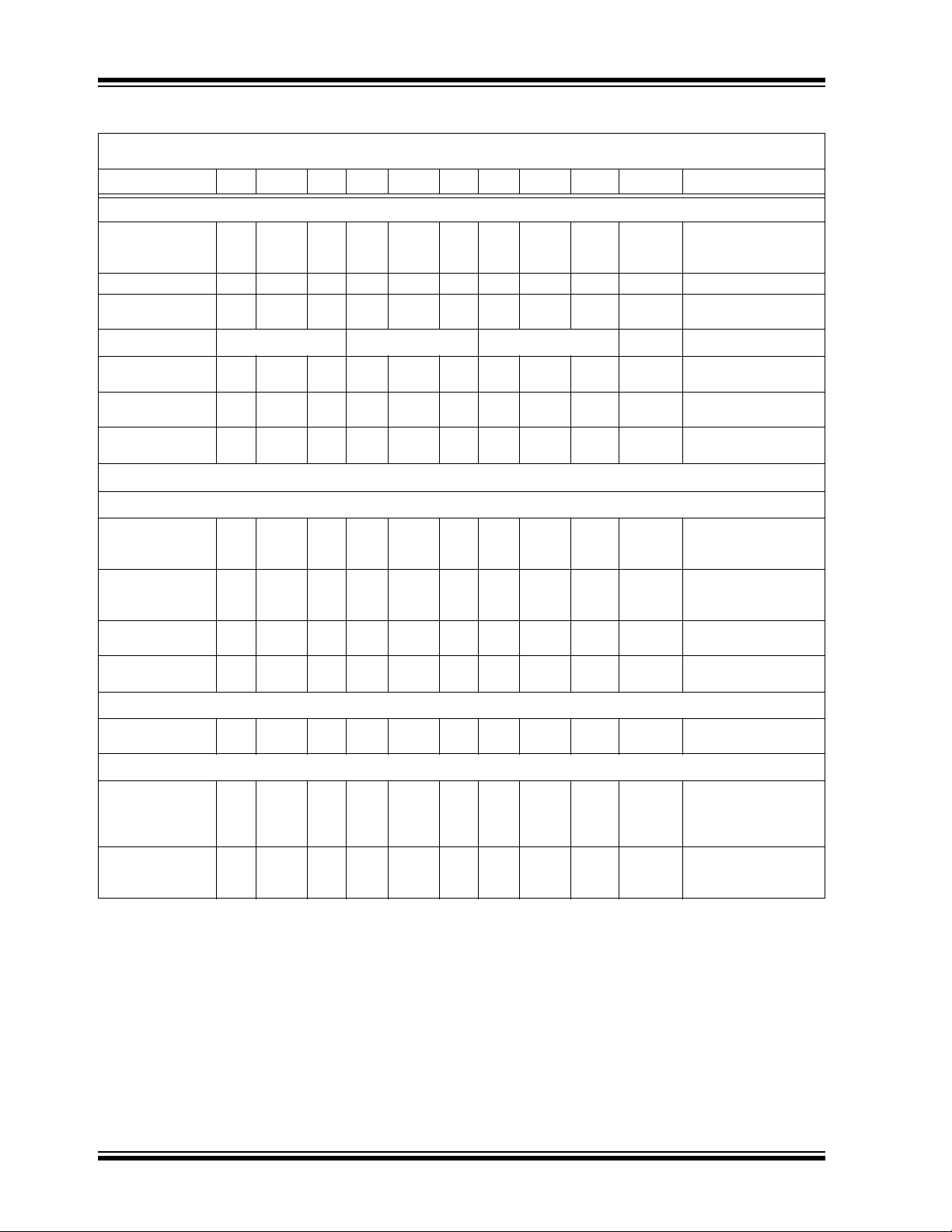
TC940X ELECTRICAL SPECIFICATIONS (CONTINUED)
Electrical Characteristics: unless otherwise specified, VDD = +5V, VSS = -5V, V
10 kHz. T
= +25°C, unless temperature range is specified (-40°C to +85°C for E device, 0°C to +70°C for C device).
A
Parameter Min Typ Max Min Typ Max Min Typ Max Units Test Conditions
Analog Input
I
Full Scale — 10 — — 10 — — 10 — µA Full Scale Analog Input
IN
I
Over Range — — 50 — — 50 — — 50 µA Over Range Current
IN
Response Time — 2 — — 2 — — 2 — Cycle Settling Time to 0.1%
Digital Section TC9400 TC9401 TC9402
@ IOL = 10mA — 0.2 0.4 — 0.2 0.4 — 0.2 0.4 V Logic “0” Output
V
SAT
V
– V
OUTMAX
Common (Note 4)
OUT
Pulse Frequency
— — 18 — — 18 — — 18 V Voltage Range Between
—3——3——3 — µs
Output Width
Frequency-to-Voltage
Supply Current
I
Quiescent
DD
(Note 5)
I
Quiescent
SS
(Note 5)
V
Supply 4 — 7.5 4 — 7.5 4 — 7.5 V Operating Range of
DD
Supply -4 — -7.5 -4 — -7.5 -4 — -7.5 V Operating Range of
V
SS
Reference Voltage
V
– V
REF
SS
Accuracy
Non-Linearity
(Note 10)
Input Frequency
Range
(Notes 7 and 8)
Note 1: Full temperature range; not tested.
2: I
= 0.
IN
3: Full temperature range, I
4: I
OUT
5: Threshold Detect = 5V, Amp Out = 0V, full temperature range.
6: 10 Hz to 100 kHz; not tested.
7: 5 µs minimum positive pulse width and 0.5 µs minimum negative pulse width.
8: t
= tF = 20 ns.
R
9: R
≥ 2kΩ, tested @ 10 kΩ.
L
10: Full temperature range, V
— 1.5 6 — 1.5 6 — 3 10 mA Current Required from
— -1.5 -6 — -1.5 -6 — -3 -10 mA Current Required from
-2.5 — — -2.5 — — -2.5 — — V Range of Voltage
— 0.02 0.05 — 0.01 0.02 — 0.05 0.25 %
10 — 100k 10 — 100k 10 — 100k Hz Frequency Range for
= 10 mA.
= 10 µA.
OUT
= -0.1V.
IN
GND
= 0V, V
= -5V, R
REF
Full Scale
= 100 kΩ, Full Scale =
BIAS
Current to achieve
Specified Accuracy
Full Scale
Voltage (Note 3)
Output and Common
Positive Supply during
Operation
Negative Supply during
Operation
Positive Supply
Negative Supply
Reference Input
Deviation from ideal
Transfer Function as a
Percentage Full Scale
Voltage
Specified Non-Linearity
DS21483D-page 4 © 2007 Microchip Technology Inc.
TC9400/9401/9402
TC940X ELECTRICAL SPECIFICATIONS (CONTINUED)
Electrical Characteristics: unless otherwise specified, VDD = +5V, VSS = -5V, V
10 kHz. T
= +25°C, unless temperature range is specified (-40°C to +85°C for E device, 0°C to +70°C for C device).
A
Parameter Min Typ Max Min Typ Max Min Typ Max Units Test Conditions
Frequency Input
Positive Excursion 0.4 — V
0.4 — V
DD
0.4 — V
DD
Negative Excursion -0.4 -2 -0.4 — -2 -0.4 — -2 V Voltage Required to
Minimum Positive
—5——5——5 — μs Time between
Pulse Width
(Note 8)
Minimum Negative
— 0.5 — — 0.5 — — 0.5 — μs Time Between
Pulse Width
(Note 8)
Input Impedance — 10 — — 10 — — 10 MΩ
Analog Outputs TC9400 TC9401 TC9402
Output Voltage
(Note 9)
—V
DD
– 1 — — V
– 1 — — V
DD
Output Loading 2 — — 2 — — 2 — — kΩ Resistive Loading at
Supply Current TC9400 TC9401 TC9402
I
Quiescent
DD
(Note 10)
I
Quiescent
SS
(Note 10)
V
Supply 4 — 7.5 4 — 7.5 4 — 7.5 V Operating Range of
DD
Supply -4 — -7.5 -4 — -7.5 -4 — -7.5 V Operating Range of
V
SS
— 1.5 6 — 1.5 6 — 3 10 mA Current Required from
— -1.5 -6 -1.5 -6 — -3 -10 mA Current Required from
Reference Voltage
V
REF
– V
SS
-2.5 — — -2.5 — — -2.5 — — V Range of Voltage
Note 1: Full temperature range; not tested.
2: I
= 0.
IN
3: Full temperature range, I
4: I
= 10 µA.
OUT
OUT
= 10 mA.
5: Threshold Detect = 5V, Amp Out = 0V, full temperature range.
6: 10 Hz to 100 kHz; not tested.
7: 5 µs minimum positive pulse width and 0.5 µs minimum negative pulse width.
8: t
= tF = 20 ns.
R
9: R
≥ 2kΩ, tested @ 10 kΩ.
L
10: Full temperature range, V
= -0.1V.
IN
GND
= 0V, V
DD
REF
= -5V, R
= 100 kΩ, Full Scale =
BIAS
V Voltage Required to
Turn Threshold
Detector On
Turn Threshold
Detector Off
Threshold Crossings
Threshold Crossings
– 1 — V Voltage Range of Op
DD
Amp Output for
Specified Non-Linearity
Output of Op Amp
Positive Supply During
Operation
Negative Supply During
Operation
Positive Supply
Negative Supply
Reference Input
© 2007 Microchip Technology Inc. DS21483D-page 5

TC9400/9401/9402
2.0 PIN DESCRIPTIONS
The descriptions of the pins are listed in Table 2-1.
TABLE 2-1: PIN FUNCTION TABLE
Pin No. Symbol Description
1I
2 ZERO ADJ Low frequency adjustment input.
3I
4V
5V
6 GND Analog ground.
7V
8 PULSE FREQ
9OUTPUT
10 FREQ/2 OUT This open drain output is a square wave at one-half the frequency of the pulse output
11 THRESHOLD
12 AMPLIFIER OUT Output of the integrator amplifier.
13 NC No internal connection.
14 V
BIAS
IN
SS
OUT Reference capacitor connection.
REF
REF
OUT
COMMON
DETECTOR
DD
This pin sets bias current in the TC9400. Connect to VSS through a 100 kΩ resistor.
Input current connection for the V/F converter.
Negative power supply voltage connection, typically -5V.
Voltage reference input, typically -5V.
Frequency output. This open drain output will pulse LOW each time the Freq.
Threshold Detector limit is reached. The pulse rate is proportional to input voltage.
Source connection for the open drain output FETs.
(Pin 8). Output transitions of this pin occur on the rising edge of Pin 8.
Input to the Threshold Detector. This pin is the frequency input during F/V operation.
Positive power supply connection, typically +5V.
2.1 Bias Current (I
BIAS
)
An external resistor, connected to VSS, sets the bias
point for the TC9400. Specifications for the TC9400 are
based on R
= 100 kΩ ±10%, unless otherwise
BIAS
noted.
Increasing the maximum frequency of the TC9400
beyond 100 kHz is limited by the pulse width of the
pulse output (typically 3 µs). Reducing R
BIAS
will
decrease the pulse width and increase the maximum
operating frequency, but linearity errors will also
increase. R
can be reduced to 20 kΩ, which will
BIAS
typically produce a maximum full scale frequency of
500 kHz.
2.2 Zero Adjust
This pin is the non-inverting input of the operational
amplifier. The low frequency set point is determined by
adjusting the voltage at this pin.
2.3 Input Current (IIN)
The inverting input of the operational amplifier and the
summing junction when connected in the V/F mode. An
input current of 10 μA is specified, but an over range
current up to 50 μA can be used without detrimental
effect to the circuit operation. I
junction of an operational amplifier. Voltage sources
cannot be attached directly, but must be buffered by
external resistors.
connects the summing
IN
2.4 Voltage Capacitor (V
The charging current for C
is supplied through this
REF
REF
Out)
pin. When the op amp output reaches the threshold
level, this pin is internally connected to the reference
x C
voltage and a charge, equal to V
REF
, is removed
REF
from the integrator capacitor. After about 3μsec, this pin
is internally connected to the summing junction of the
op amp to discharge C
. Break-before-make switch-
REF
ing ensures that the reference voltage is not directly
applied to the summing junction.
2.5 Voltage Reference (V
REF
)
A reference voltage from either a precision source, or
the V
supply is applied to this pin. Accuracy of the
SS
TC9400 is dependent on the voltage regulation and
temperature characteristics of the reference circuitry.
Since the TC9400 is a charge balancing V/F converter,
the reference current will be equal to the input current.
For this reason, the DC impedance of the reference
voltage source must be kept low enough to prevent
linearity errors. For linearity of 0.01%, a reference
impedance of 200Ω or less is recommended. A 0.1 µF
bypass capacitor should be connected from V
REF
ground.
to
DS21483D-page 6 © 2007 Microchip Technology Inc.
TC9400/9401/9402
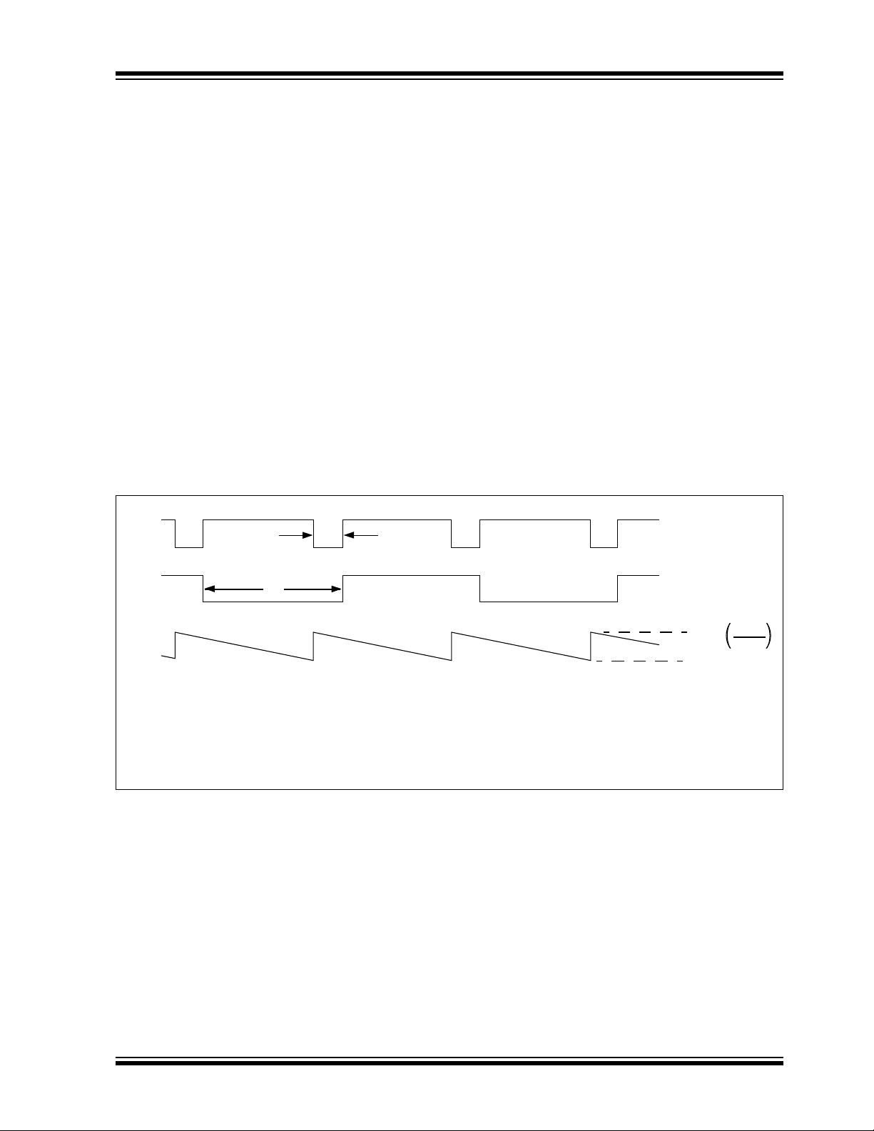
3ms
Typ.
1/f
F
OUT
F
OUT
/2
Amp Out
V
REF
0V
C
REF
C
INT
Note 1: To adjust F
MIN
, set VIN = 10 mV and adjust the 50 kΩ offset for 10 Hz output.
2: To adjust F
MAX
, set VIN = 10V and adjust RIN or V
REF
for 10 kHz output.
3: To increase F
OUTMAX
to 100 kHz, change C
REF
to 2 pF and C
INT
to 75 pF.
4: For high performance applications, use high stability components for R
IN
, C
REF
. V
REF
(metal film
resistors and glass capacitors). Also, separate output ground (Pin 9) from input ground (Pin 6).
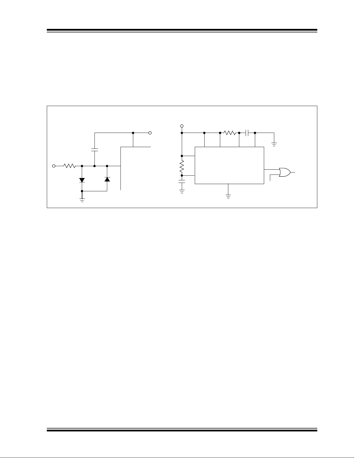
2.6 Pulse Freq Out
This output is an open-drain N-channel FET, which
provides a pulse waveform whose frequency is proportional to the input voltage. This output requires a pullup resistor and interfaces directly with MOS, CMOS,
and TTL logic (see Figure 2-1).
2.7 Output Common
The sources of both the FREQ/2 OUT and the PULSE
FREQ OUT are connected to this pin. An output level
swing from the drain voltage to ground, or to the V
SS
supply, may be obtained by connecting this pin to the
appropriate point.
2.8 Freq/2 Out
This output is an open-drain N-channel FET, which
provides a square-wave one-half the frequency of the
pulse frequency output. The FREQ/2 OUT output will
change state on the rising edge of PULSE FREQ OUT.
This output requires a pull-up resistor and interfaces
directly with MOS, CMOS, and TTL logic.
2.9 Threshold Detector Input
In the V/F mode, this input is connected to the AMPLIFIER OUT output (Pin 12) and triggers a 3 µs pulse
when the input voltage passes through its threshold. In
the F/V mode, the input frequency is applied to this
input.
The nominal threshold of the detector is half way
between the power supplies, or (V
+ VSS)/2 ±400
DD
mV. The TC9400’s charge balancing V/F technique is
not dependent on a precision comparator threshold,
because the threshold only sets the lower limit of the op
amp output. The op amp’s peak-to-peak output swing,
which determines the frequency, is only influenced by
external capacitors and by V
REF
.
2.10 Amplifier Out
This pin is the output stage of the operational amplifier.
During V/F operation, a negative going ramp signal is
available at this pin. In the F/V mode, a voltage
proportional to the frequency input is generated.
FIGURE 2-1: Output Waveforms.
© 2007 Microchip Technology Inc. DS21483D-page 7
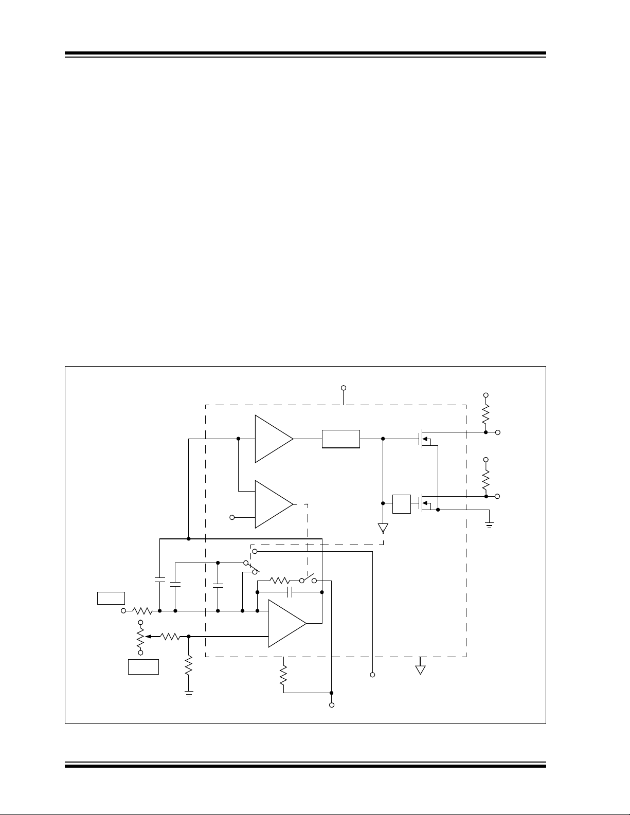
TC9400/9401/9402
–
+
+5V
+
5V
14
V
DD
+
5V
R
L
10 kΩ
R
L
10 kΩ
8
10
9
F
OUT
F
OUT
/2
11
3ms
Delay
Self-
Star t
12
5
20 kΩ
60 pF
Op Amp
C
INT
820 pF
C
REF
180 pF
12 pF
R
IN
1MΩ
V
IN
+5V
-5V
50 kΩ
510 kΩ
10 kΩ
3
1
Offset
Adjust
I
IN
Zero Adjust
0V –10V
I
BIAS
V
SS
4
-5V
2
Output
Common
V
REF
OUT
R
BIAS
100 kΩ
AMP OUT
TC9400
TC9401
TC9402
GND
6
Threshold
Detector
Threshold
Detect
Reference Voltage
(Typically -5V)
÷2
V
REF
7
-3V
INPUT
3.0 DETAILED DESCRIPTION
3.1 Voltage-to-Frequency (V/F) Circuit
Description
The TC9400 V/F converter operates on the principal of
charge balancing. The operation of the TC9400 is
easily understood by referring to Figure 3-1. The input
voltage (V
resistor. This current is then converted to a charge on
the integrating capacitor and shows up as a linearly
decreasing voltage at the output of the op amp. The
lower limit of the output swing is set by the threshold
detector, which causes the reference voltage to be
applied to the reference capacitor for a time period long
enough to charge the capacitor to the reference voltage. This action reduces the charge on the integrating
capacitor by a fixed amount (q = C
the op amp output to step up a finite amount.
At the end of the charging period, C
This dissipates the charge stored on the reference
capacitor, so that when the output again crosses zero,
the system is ready to recycle. In this manner, the continued discharging of the integrating capacitor by the
input is balanced out by fixed charges from the refer-
) is converted to a current (IIN) by the input
IN
x V
REF
REF
), causing
REF
is shorted out.
ence voltage. As the input voltage is increased, the
number of reference pulses required to maintain
balance increases, which causes the output frequency
to also increase. Since each charge increment is fixed,
the increase in frequency with voltage is linear. In
addition, the accuracy of the output pulse width does
not directly affect the linearity of the V/F. The pulse
must simply be long enough for full charge transfer to
take place.
The TC9400 contains a “self-start” circuit to ensure the
V/F converter always operates properly when power is
first applied. In the event that, during power-on, the op
amp output is below the threshold and C
is already
REF
charged, a positive voltage step will not occur. The op
amp output will continue to decrease until it crosses the
-3.0V threshold of the “self-start” comparator. When
this happens, an internal resistor is connected to the op
amp input, which forces the output to go positive until
the TC9400 is in its normal Operating mode.
The TC9400 utilizes low-power CMOS processing for
low input bias and offset currents, with very low power
dissipation. The open drain N-channel output FETs
provide high voltage and high current sink capability.
FIGURE 3-1: 10 Hz to 10 kHz V/F Converter.
DS21483D-page 8 © 2007 Microchip Technology Inc.

3.2 Voltage-to-Time Measurements
The TC9400 output can be measured in the time
domain as well as the frequency domain. Some microcomputers, for example, have extensive timing capability, but limited counter capability. Also, the response
time of a time domain measurement is only the period
between two output pulses, while the frequency
measurement must accumulate pulses during the
entire counter time-base period.
Time measurements can be made from either the
TC9400’s PULSE FREQ OUT output, or from the
FREQ/2 OUT output. The FREQ/2 OUT output
changes state on the rising edge of PULSE FREQ
OUT, so FREQ/2 OUT is a symmetrical square wave at
one-half the pulse output frequency. Timing measurements can, therefore, be made between successive
PULSE FREQ OUT pulses, or while FREQ/2 OUT is
high (or low).
TC9400/9401/9402
© 2007 Microchip Technology Inc. DS21483D-page 9

TC9400/9401/9402
Frequency Out
V
IN
R
IN
--------
1
V
REF
()C
REF
()
------------------------------------
•
=
VIN
FULL SCALE
10 μA
RIN ≅
10V
10
μ
A
RIN ≅ = 1 M
Ω
4.0 VOLTAGE-TO-FREQUENCY
(V/F) CONVERTER DESIGN
INFORMATION
4.1 Input/Output Relationships
The output frequency (F
input voltage (V
) by the transfer equation:
IN
EQUATION 4-1:
4.2 External Component Selection
4.2.1 R
The value of this component is chosen to give a full
scale input current of approximately 10 µA:
EQUATION 4-2:
EQUATION 4-3:
IN
) is related to the analog
OUT
4.2.3 C
REF
The exact value is not critical and may be used to trim
the full scale frequency (see Section 6.1 “Input/Out-
put Relationships”, Input/Output Relationships).
Glass film or air trimmer capacitors are recommended
because of their stability and low leakage. Locate as
close as possible to Pins 5 and 3 (see Figure 4-1).
500
400
300
(pF) +12pF
200
REF
C
100
0
10 kHz
100 kHz
-2 -3 -4 -5 -6 -7
-1
V
REF
FIGURE 4-1: Recommended C
V
.
REF
4.2.4 V
DD
, V
SS
(V)
V
DD
V
SS
R
IN
V
IN
T
A
= +5V
= -5V
= 1MW
= +10V
= +25°C
REF
vs.
Power supplies of ±5V are recommended. For high
accuracy requirements, 0.05% line and load regulation
and 0.1 µF disc decoupling capacitors, located near the
pins, are recommended.
Note that the value is an approximation and the exact
relationship is defined by the transfer equation. In
practice, the value of R
typically would be trimmed to
IN
obtain full scale frequency at VIN full scale (see
Section 4.3 “Adjustment Procedure”, Adjustment
Procedure). Metal film resistors with 1% tolerance or
better are recommended for high accuracy applications
because of their thermal stability and low noise
generation.
4.2.2 C
The exact value is not critical but is related to C
INT
REF
by
the relationship:
≤
C
3C
REF
INT
≤ 10C
REF
Improved stability and linearity are obtained when
≤ 4C
C
INT
. Low leakage types are recommended,
REF
although mica and ceramic devices can be used in
applications where their temperature limits are not
exceeded. Locate as close as possible to Pins 12
and 13.
4.3 Adjustment Procedure
Figure 3-1 shows a circuit for trimming the zero
location. Full scale may be trimmed by adjusting R
V
REF
, or C
. Recommended procedure for a 10 kHz
REF
IN
full scale frequency is as follows:
1. Set V
to 10 mV and trim the zero adjust circuit
IN
to obtain a 10 Hz output frequency.
2. Set V
to 10V and trim either RIN, V
IN
REF
, or C
REF
to obtain a 10 kHz output frequency.
If adjustments are performed in this order, there should
be no interaction and they should not have to be
repeated.
4.4 Improved Single Supply V/F
Converter Operation
A TC9400, which operates from a single 12 to 15V
variable power source, is shown in Figure 4-2. This
circuit uses two Zener diodes to set stable biasing
levels for the TC9400. The Zener diodes also provide
the reference voltage, so the output impedance and
temperature coefficient of the Zeners will directly affect
power supply rejection and temperature performance.
Full scale adjustment is accomplished by trimming the
input current.
,
DS21483D-page 10 © 2007 Microchip Technology Inc.

TC9400/9401/9402
R1
910 kΩ
R4
1µF
D2
5.1 VZ
R2
910 kΩ
R5
91 kΩ
Rp
Offset
20 kΩ
100 kΩ
D1
5.1 VZ
0.1 µF
100 kΩ
C
REF
C
INT
1.2 kΩ
+12 to +15V
10 10 kΩ
Output
Frequency
Digital
Ground
Analog Ground
Input
Voltage
(0 to 10V)
R3
Gain
TC9400
11
12
5
3
2
6
7
1
4
14
9
10
8
Threshold
Detect
Amp Out
C
REF
I
IN
Zero Adjust
GND
V
REF
I
BIAS
Output
Common
F
OUT
/2
F
OUT
V
DD
V
SS
100 kΩ
kΩ
Component Selection
F/S Freq. C
REF
C
INT
1 kHz 2200 pF 4700 pF
10 kHz 180 pF 470 pF
100 kHz 27 pF 75 pF
Trimming the reference voltage is not recommended
for high accuracy applications unless an op amp is
used as a buffer, because the TC9400 requires a lowimpedance reference (see Section 2.5 “Voltage Ref-
erence (VREF)”, V
pin description, for more infor-
REF
mation).
The circuit of Figure 4-2 will directly interface with
CMOS logic operating at 12V to 15V. TTL or 5V CMOS
logic can be accommodated by connecting the output
pull-up resistors to the +5V supply. An optoisolator can
also be used if an isolated output is required; also, see
Figure 4-3.
FIGURE 4-2: Voltage-to-Frequency.
© 2007 Microchip Technology Inc. DS21483D-page 11

TC9400/9401/9402
V+ = 8V to 15V (Fixed)
14
8
10 kΩ
10 kΩ
F
OUT
F
OUT
/2
10
149
100 kΩ
0V–10V
I
IN
180
pF
820
pF
3
5
12
11
7
0.01
µF
2
kΩ
8.2
kΩ
6
2
V2
R2
0.9Ω
R1
0.2
R
1
R
IN
1MΩ
I
IN
V
REF
TC9400
Offset
Adjust
Gain
Adjust
5V
0.01
µF
V
IN
V+ R
1
R
2
10V 1 MΩ 10 kΩ
12V 1.4 MΩ 14 kΩ
15V 2 MΩ 20 kΩ
F
OUTIIN
1
V
2V7
–()C
REF
()
----------------------------------------- -
=
I
IN
VINV2–()
R
IN
------------------------- -
V+ V
2
–()
0.9R
1
0.2R
1
+()
-------------------------------------- -+=
FIGURE 4-3: Fixed Voltage – Single Supply Operation.
DS21483D-page 12 © 2007 Microchip Technology Inc.

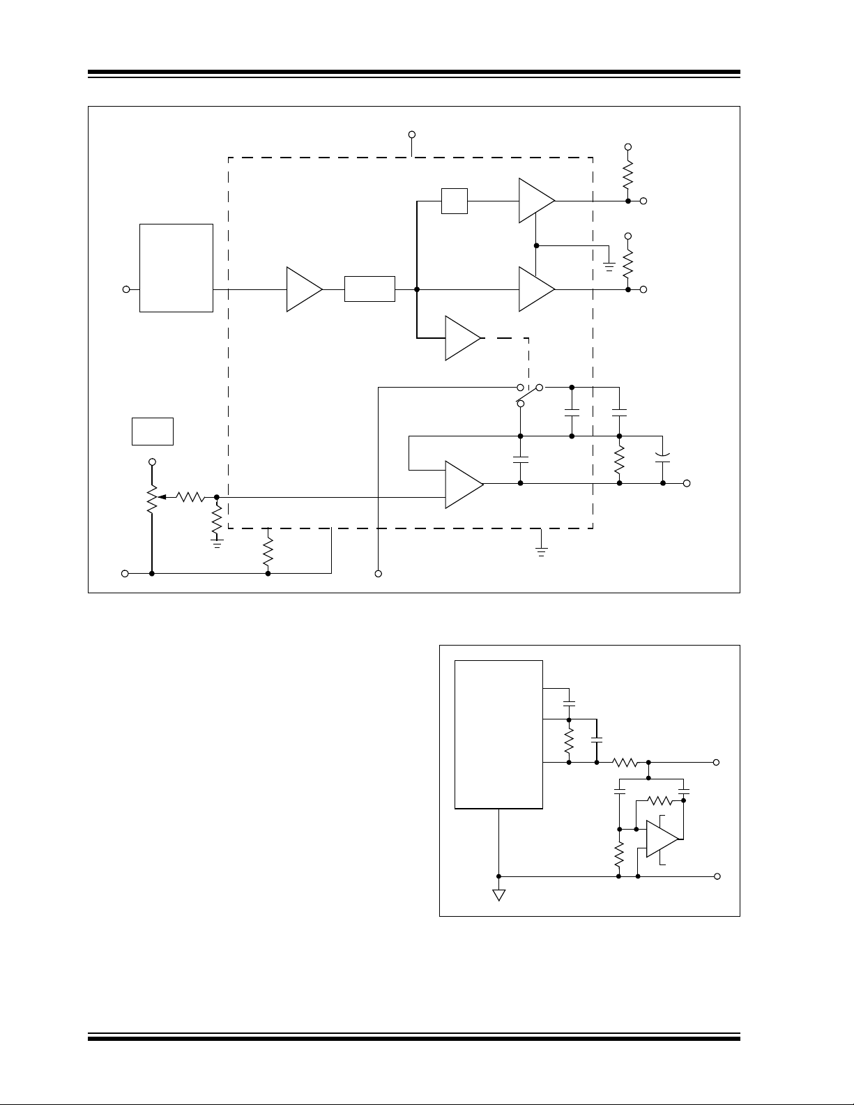
5.0 FREQUENCY-TO-VOLTAGE (F/V) CIRCUIT DESCRIPTION
When used as an F/V converter, the TC9400 generates
an output voltage linearly proportional to the input
frequency waveform.
Each zero crossing at the threshold detector’s input
causes a precise amount of charge (q = C
to be dispensed into the op amp’s summing junction.
This charge, in turn, flows through the feedback
resistor, generating voltage pulses at the output of the
op amp. A capacitor (C
pulses into a DC voltage, which is linearly proportional
to the input frequency.
) across R
INT
INT
x V
REF
averages these
REF
TC9400/9401/9402
)
© 2007 Microchip Technology Inc. DS21483D-page 13

TC9400/9401/9402
V
OUT
= [V
REF CREF RINT
] F
IN
+5V
14
64
+5V
-5V
V
DD
1.0
11
33 kΩ
IN914
V
SS
DET
TC9400
(a) ±5V Supply
(b) Single Supply
0.01 µF
Frequency
Input
0V
GND
+8V to +15V
14
10 kΩ
4
+5V
V
DD
1.0
11
33 kΩ
IN914
V
SS
DET
TC9400
0.01 µF
Frequency
Input
0V
0.1 µF
10 kΩ
MΩ
MΩ
6.0 F/V CONVERTER DESIGN INFORMATION
6.1 Input/Output Relationships
The output voltage is related to the input frequency
(FIN) by the transfer equation:
EQUATION 6-1:
The response time to a change in FIN is equal to (R
C
). The amount of ripple on V
INT
proportional to C
can be increased to lower the ripple. Values of
C
INT
and the input frequency.
INT
is inversely
OUT
1 µF to 100 µF are perfectly acceptable for low frequencies.
When the TC9400 is used in the Single Supply mode,
is defined as the voltage difference between Pin 7
V
REF
and Pin 2.
INT
6.2 Input Voltage Levels
The input frequency is applied to the Threshold
Detector input (Pin 11). As discussed in the V/F circuit
section of this data sheet, the threshold of Pin 11 is
approximately (V
voltage range extends from V
the threshold. If the voltage on Pin 11 goes more than
2.5 volts below the threshold, the V/F mode start-up
comparator will turn on and corrupt the output voltage.
The Threshold Detector input has about 200 mV of
hysteresis.
In ±5V applications, the input voltage levels for the
TC9400 are ±400 mV, minimum. If the frequency
source being measured is unipolar, such as TTL or
CMOS operating from a +5V source, then an AC
coupled level shifter should be used. One such circuit
is shown in Figure 6-1(a).
The level shifter circuit in Figure 6-1(b) can be used in
single supply F/V applications. The resistor divider
ensures that the input threshold will track the supply
voltages. The diode clamp prevents the input from
going far enough in the negative direction to turn on the
start-up comparator. The diode’s forward voltage
decreases by 2.1 mV/°C, so for high ambient
temperature operation, two diodes in series are
recommended.
+ VSS)/2 ±400 mV. Pin 11’s input
DD
to about 2.5V below
DD
FIGURE 6-1: Frequency Input Level Shifter.
DS21483D-page 14 © 2007 Microchip Technology Inc.

TC9400/9401/9402
Offset
Adjust
10 kΩ
.01 µF
6.2V
IN914
33 kΩ
100 kΩ
500 kΩ
0.1 µF
100 kΩ
V+ = 10V to 15V
1
47 pF
V
OUT
Frequency
Input
TC9400
6
10 kΩ
2
11
1.0
4
14
12
3
5
GND
V
REF
OUT
I
IN
Zero
Adjust
V
REF
I
BIAS
Amp Out
V
DD
V
SS
GND
6
7
1.0 kΩ
V+
1.0 kΩ
0.01 µF
.001 µF
DET
Note: The output is referenced to Pin 6, which is at 6.2V (Vz). For frequency meter applications,
a 1 mA meter with a series scaling resistor can be placed across Pins 6 and 12.
MΩ
MΩ
0.5 ms
Min
5.0 ms
Min
Delay = 3 ms
Input
F
OUT
F
OUT
/2
FIGURE 6-2: F/V Single Supply F/V Converter.
and F
/2 are not used in the F/V mode. How-
OUT
6.3 Input Buffer
F
OUT
ever, these outputs may be useful for some applications, such as a buffer to feed additional circuitry. Then,
will follow the input frequency waveform, except
F
OUT
that F
will go high 3 µs after FIN goes high; F
OUT
will be square wave with a frequency of one-half F
/2
OUT
OUT
.
FIGURE 6-3: F/V Digital Outputs.
If these outputs are not used, Pins 8, 9 and 10 should be
connected to ground (see Figure 6-3 and Figure 6-4).
© 2007 Microchip Technology Inc. DS21483D-page 15
TC9400/9401/9402
TC9400A
TC9401A
TC9402A
+5V
14
V
DD
V+
V+
F
OUT
/2
F
OUT
Output
Common
10
9
8
5
3
12
12 pF
C
REF
56 pF
C
INT
1000 pF
R
INT
1MΩ
60 pF
Amp
Out
V
OUT
V
SS
I
BIAS
14
10 kΩ
2.2 kΩ
100 kΩ
2kΩ
-5V
+5V
Zero Adjust
2
7
(Typically -5V)
V
REF
F
IN
11
Threshold
Detector
3ms
Delay
*
*
*
*Optional If
Buffer is Needed
Offset
Adjust
V
REF
OUT
I
IN
42
–
+
Op
Amp
+
V
REF
See
Figure 7-1:
Frequency
Input Level
Shifter
6
GND
Threshold
Detect
1
47 pF
V
OUT
TC9400
12
3
5
V
REF
OUT
I
IN
GND
AMP OUT
6
.001 µF
+
–
1
3
2
.01 µF
1MΩ
0.1 µF
+5
7
6
4
-5
TL071
200Ω
MΩ
MΩ
FIGURE 6-4: DC – 10 kHz Converter.
6.4 Output Filtering
The output of the TC9400 has a sawtooth ripple superimposed on a DC level. The ripple will be rejected if the
TC9400 output is converted to a digital value by an
integrating Analog-to-Digital Converter, such as the
TC7107. The ripple can also be reduced by increasing
the value of the integrating capacitor, although this will
reduce the response time of the F/V converter.
The sawtooth ripple on the output of an F/V can be
eliminated without affecting the F/V’s response time by
using the circuit in Figure 6-1. The circuit is a
capacitance multiplier, where the output coupling
capacitor is multiplied by the AC gain of the op amp. A
moderately fast op amp, such as the TL071, should be
used.
DS21483D-page 16 © 2007 Microchip Technology Inc.
FIGURE 6-5: Ripple Filter.
TC9400/9401/9402
V
DD
14
11
1000 pF
Threshold
Detector
1kΩ
F
IN
V
DD
100 kΩ
1µF
3
4
8
6
F
IN
12516
V
CC
B R C
Q
V
SS
A
CLRA
CD4538
TC9400
(a) (b)
To TC9400
7.0 F/V POWER-ON RESET
In F/V mode, the TC9400 output voltage will occasionally be at its maximum value when power is first
applied. This condition remains until the first pulse is
applied to F
applications, this is not a problem because proper
operation begins as soon as the frequency input is
applied.
. In most frequency measurement
IN
In some cases, however, the TC9400 output must be
zero at power-on without a frequency input. In such
cases, a capacitor connected from Pin 11 to V
usually be sufficient to pulse the TC9400 and provide a
Power-on Reset (see Figure 7-1 (a) and (b)). Where
predictable power-on operation is critical, a more
complicated circuit, such as Figure 7-1 (b), may be
required.
DD
will
FIGURE 7-1: Power-On Operation/Reset.
© 2007 Microchip Technology Inc. DS21483D-page 17

TC9400/9401/9402
Legend: XX...X Customer-specific information
Y Year code (last digit of calendar year)
YY Year code (last 2 digits of calendar year)
WW Week code (week of January 1 is week ‘01’)
NNN Alphanumeric traceability code
Pb-free JEDEC designator for Matte Tin (Sn)
* This package is Pb-free. The Pb-free JEDEC designator ( )
can be found on the outer packaging for this package.
Note: In the event the full Microchip part number cannot be marked on one line, it will
be carried over to the next line, thus limiting the number of available
characters for customer-specific information.
3
e
XXXXXXXXXXXXXX
YYWWNNN
14-Lead CERDIP
XXXXXXXXXXXXXX
0731256
Example: (Front View)
TC9400EJD
14-Lead PDIP
XXXXXXXXXXXXXX
XXXXXXXXXXXXXX
YYWWNNN
Example: (Front View)
14-Lead SOIC (.150”)
XXXXXXXXXXX
XXXXXXXXXXX
YYWWNNN
Example: (Front View)
Y2026
Example: (Back View)
Y2026
Example: (Back View)
TC9400
CPD ^^
0731256
TC9400
EOD
^^
0731256
Example: (Back View)
Y2026
8.0 PACKAGE INFORMATION
8.1 Package Marking Information
3
e
3
e
DS21483D-page 18 © 2007 Microchip Technology Inc.
3
e
TC9400/9401/9402
14-Lead Ceramic Dual In-Line (JD) – .300" Body [CERDIP]
B
Note: For the most current package drawings, please see the Microchip Packaging Specification located at
http://www.microchip.com/packaging
N
NOTE 1
1
2
D
A
A1
b1
b
Number of Pins N 14
Pitch e .100 BSC
Top to Seating Plane A – – .200
Standoff § A1 .015 – –
Ceramic Package Height A2 .140 – .175
Shoulder to Shoulder Width E .290 – .325
Ceramic Package Width E1 .230 .288 .300
Overall Length D .740 .760 .780
Tip to Seating Plane L .125 – .200
Lead Thickness c .008 – .015
Upper Lead Width b1 .045 – .065
Lower Lead Width b .015 – .023
Overall Row Spacing E2 .320 – .410
Notes:
1. Pin 1 visual index feature may vary, but must be located within the hatched area.
2. § Significant Characteristic.
3. Dimensioning and tolerancing per ASME Y14.5M.
BSC: Basic Dimension. Theoretically exact value shown without tolerances.
e
Dimension Limits MIN NOM MAX
E1
A2
L
Units INCHES
Microchip Technology Drawing C04-002
E
c
E2
© 2007 Microchip Technology Inc. DS21483D-page 19
TC9400/9401/9402
14-Lead Plastic Dual In-Line (PD) – 300 mil Body [PDIP]
Notes:
1. Pin 1 visual index feature may vary, but must be located with the hatched area.
2. § Significant Characteristic.
3. Dimensions D and E1 do not include mold flash or protrusions. Mold flash or protrusions shall not exceed .010" per side.
4. Dimensioning and tolerancing per ASME Y14.5M.
BSC: Basic Dimension. Theoretically exact value shown without tolerances.
Note: For the most current package drawings, please see the Microchip Packaging Specification located at
http://www.microchip.com/packaging
Units INCHES
Dimension Limits MIN NOM MAX
Number of Pins N 14
Pitch e .100 BSC
Top to Seating Plane A – – .210
Molded Package Thickness A2 .115 .130 .195
Base to Seating Plane A1 .015 – –
Shoulder to Shoulder Width E .290 .310 .325
Molded Package Width E1 .240 .250 .280
Overall Length D .735 .750 .775
Tip to Seating Plane L .115 .130 .150
Lead Thickness c .008 .010 .015
Upper Lead Width b1 .045 .060 .070
Lower Lead Width b .014 .018 .022
Overall Row Spacing § eB – – .430
N
E1
D
NOTE 1
12
3
E
c
eB
A2
L
A
A1
b1
b e
Microchip Technology Drawing C04-005B
DS21483D-page 20 © 2007 Microchip Technology Inc.
TC9400/9401/9402
14-Lead Plastic Small Outline (OD) – Narrow, 3.90 mm Body [SOIC]
Notes:
1. Pin 1 visual index feature may vary, but must be located within the hatched area.
2. § Significant Characteristic.
3. Dimensions D and E1 do not include mold flash or protrusions. Mold flash or protrusions shall not exceed 0.15 mm per side.
4. Dimensioning and tolerancing per ASME Y14.5M.
BSC: Basic Dimension. Theoretically exact value shown without tolerances.
REF: Reference Dimension, usually without tolerance, for information purposes only.
Note: For the most current package drawings, please see the Microchip Packaging Specification located at
http://www.microchip.com/packaging
Units MILLIMETERS
Dimension Limits MIN NOM MAX
Number of Pins N 14
Pitch e 1.27 BSC
Overall Height A – – 1.75
Molded Package Thickness A2 1.25 – –
Standoff § A1 0.10 – 0.25
Overall Width E 6.00 BSC
Molded Package Width E1 3.90 BSC
Overall Length D 8.65 BSC
Chamfer (optional) h 0.25 – 0.50
Foot Length L 0.40 – 1.27
Footprint L1 1.04 REF
Foot Angle φ 0° – 8°
Lead Thickness c 0.17 – 0. 25
Lead Width b 0.31 – 0. 51
Mold Draft Angle Top α 5° – 15°
Mold Draft Angle Bottom β 5° – 15°
NOTE 1
N
D
E
E1
1
2 3
b
e
A
A1
A2
L
L1
c
h
h
α
β
φ
Microchip Technology Drawing C04-065B
© 2007 Microchip Technology Inc. DS21483D-page 21

TC9400/9401/9402
NOTES:
DS21483D-page 22 © 2007 Microchip Technology Inc.

APPENDIX A: REVISION HISTORY
Revision D (September 2007)
The following is the list of modifications:
1. Corrected Figure 6-1.
2. Added History section.
3. Updated package marking information and
package outline drawings
4. Added Product identification System section.
Revision C (May 2006)
Revision B (May 2002)
Revision A (April 2002)
• Original Release of this Document.
TC9400/9401/9402
© 2007 Microchip Technology Inc. DS21483D-page 23

TC9400/9401/9402
NOTES:
DS21483D-page 24 © 2007 Microchip Technology Inc.

TC9400/9401/9402
PART NO. X /XX
PackageTemperature
Range
Device
Device TC9400: Voltage-to-Frequency Converter
TC9401: Voltage-to-Frequency Converter
TC9402: Voltage-to-Frequency Converter
Temperature Range E = -40°C to +85°C (Extended)
C=0°C to +70°C (Commercial)
Package JD = Ceramic Dual-Inline (.300” Body), 14-lead
PD = Plastic Dual-Inline (300 mil Body), 14-lead
OD = Plastic Small Outline (3.90 MM Body), 14-lead
OD713 = Plastic Small Outline (3.90 MM Body), 14-lead
Tape and Reel.
Examples:
a) TC9400COD: 0°C to +70°C,
14LD SOIC package.
b) TC9400COD713:0°C to +70°C,
14LD SOIC package,
Tape and Reel
c) TC9400CPD: 0°C to +70°C,
14LD PDIP package.
d) TC9400EJD: -40°C to +85°C,
14LD PDIP package.
a) TC9401CPD: 0°C to +70°C,
14LD PDIP package.
b) TC9401EJD: -40°C to +85°C,
14LD CERDIP package.
a) TC9402CPD: 0°C to +70°C,
14LD PDIP package.
b) TC9402EJD: -40°C to +85°C,
14LD CERDIP package.
PRODUCT IDENTIFICATION SYSTEM
To order or obtain information, e.g., on pricing or delivery, refer to the factory or the listed sales office.
© 2007 Microchip Technology Inc. DS21483D-page 25

TC9400/9401/9402
NOTES:
DS21483D-page 26 © 2007 Microchip Technology Inc.

Note the following details of the code protection feature on Microchip devices:
• Microchip products meet the specification contained in their particular Microchip Data Sheet.
• Microchip believes that its family of products is one of the most secure families of its kind on the market today, when used in the
intended manner and under normal conditions.
• There are dishonest and possibly illegal methods used to breach the code protection feature. All of these methods, to our
knowledge, require using the Microchip products in a manner outside the operating specifications contained in Microchip’s Data
Sheets. Most likely, the person doing so is engaged in theft of intellectual property.
• Microchip is willing to work with the customer who is concerned about the integrity of their code.
• Neither Microchip nor any other semiconductor manufacturer can guarantee the security of their code. Code protection does not
mean that we are guaranteeing the product as “unbreakable.”
Code protection is constantly evolving. We at Microchip are committed to continuously improving the code protection features of our
products. Attempts to break Microchip’s code protection feature may be a violation of the Digital Millennium Copyright Act. If such acts
allow unauthorized access to your software or other copyrighted work, you may have a right to sue for relief under that Act.
Information contained in this publication regarding device
applications and the like is provided only for your convenience
and may be superseded by updates. It is your responsibility to
ensure that your application meets with your specifications.
MICROCHIP MAKES NO REPRESENTATIONS OR
WARRANTIES OF ANY KIND WHETHER EXPRESS OR
IMPLIED, WRITTEN OR ORAL, STATUTORY OR
OTHERWISE, RELATED TO THE INFORMATION,
INCLUDING BUT NOT LIMITED TO ITS CONDITION,
QUALITY, PERFORMANCE, MERCHANTABILITY OR
FITNESS FOR PURPOSE. Microchip disclaims all liability
arising from this information and its use. Use of Microchip
devices in life support and/or safety applications is entirely at
the buyer’s risk, and the buyer agrees to defend, indemnify and
hold harmless Microchip from any and all damages, claims,
suits, or expenses resulting from such use. No licenses are
conveyed, implicitly or otherwise, under any Microchip
intellectual property rights.
Trademarks
The Microchip name and logo, the Microchip logo, Accuron,
dsPIC, K
EELOQ, KEELOQ logo, microID, MPLAB, PIC,
PICmicro, PICSTART, PRO MATE, rfPIC and SmartShunt are
registered trademarks of Microchip Technology Incorporated
in the U.S.A. and other countries.
AmpLab, FilterLab, Linear Active Thermistor, Migratable
Memory, MXDEV, MXLAB, SEEVAL, SmartSensor and The
Embedded Control Solutions Company are registered
trademarks of Microchip Technology Incorporated in the
U.S.A.
Analog-for-the-Digital Age, Application Maestro, CodeGuard,
dsPICDEM, dsPICDEM.net, dsPICworks, dsSPEAK, ECAN,
ECONOMONITOR, FanSense, FlexROM, fuzzyLAB,
In-Circuit Serial Programming, ICSP, ICEPIC, Mindi, MiWi,
MPASM, MPLAB Certified logo, MPLIB, MPLINK, PICkit,
PICDEM, PICDEM.net, PICLAB, PICtail, PowerCal,
PowerInfo, PowerMate, PowerTool, REAL ICE, rfLAB, Select
Mode, Smart Serial, SmartTel, Total Endurance, UNI/O,
WiperLock and ZENA are trademarks of Microchip
Technology Incorporated in the U.S.A. and other countries.
SQTP is a service mark of Microchip Technology Incorporated
in the U.S.A.
All other trademarks mentioned herein are property of their
respective companies.
© 2007, Microchip Technology Incorporated, Printed in the
U.S.A., All Rights Reserved.
Printed on recycled paper.
Microchip received ISO/TS-16949:2002 certification for its worldwide
headquarters, design and wafer fabrication facilities in Chandler and
Tempe, Arizona; Gresham, Oregon and design centers in California
and India. The Company’s quality system processes and procedures
are for its PIC
devices, Serial EEPROMs, microperipherals, nonvolatile memory and
analog products. In addition, Microchip’s quality system for the design
and manufacture of development systems is ISO 9001:2000 certified.
®
MCUs and dsPIC® DSCs, KEELOQ
®
code hopping
© 2007 Microchip Technology Inc. DS21483D-page 27

WORLDWIDE SALES AND SERVICE
AMERICAS
Corporate Office
2355 West Chandler Blvd.
Chandler, AZ 85224-6199
Tel: 480-792-7200
Fax: 480-792-7277
Technical Support:
http://support.microchip.com
Web Address:
www.microchip.com
Atlanta
Duluth, GA
Tel: 678-957-9614
Fax: 678-957-1455
Boston
Westborough, MA
Tel: 774-760-0087
Fax: 774-760-0088
Chicago
Itasca, IL
Tel: 630-285-0071
Fax: 630-285-0075
Dallas
Addison, TX
Tel: 972-818-7423
Fax: 972-818-2924
Detroit
Farmington Hills, MI
Tel: 248-538-2250
Fax: 248-538-2260
Kokomo
Kokomo, IN
Tel: 765-864-8360
Fax: 765-864-8387
Los Angeles
Mission Viejo, CA
Tel: 949-462-9523
Fax: 949-462-9608
Santa Clara
Santa Clara, CA
Tel: 408-961-6444
Fax: 408-961-6445
Toronto
Mississauga, Ontario,
Canada
Tel: 905-673-0699
Fax: 905-673-6509
ASIA/PACIFIC
Asia Pacific Office
Suites 3707-14, 37th Floor
Tower 6, The Gateway
Harbour City, Kowloon
Hong Kong
Tel: 852-2401-1200
Fax: 852-2401-3431
Australia - Sydney
Tel: 61-2-9868-6733
Fax: 61-2-9868-6755
China - Beijing
Tel: 86-10-8528-2100
Fax: 86-10-8528-2104
China - Chengdu
Tel: 86-28-8665-5511
Fax: 86-28-8665-7889
China - Fuzhou
Tel: 86-591-8750-3506
Fax: 86-591-8750-3521
China - Hong Kong SAR
Tel: 852-2401-1200
Fax: 852-2401-3431
China - Qingdao
Tel: 86-532-8502-7355
Fax: 86-532-8502-7205
China - Shanghai
Tel: 86-21-5407-5533
Fax: 86-21-5407-5066
China - Shenyang
Tel: 86-24-2334-2829
Fax: 86-24-2334-2393
China - Shenzhen
Tel: 86-755-8203-2660
Fax: 86-755-8203-1760
China - Shunde
Tel: 86-757-2839-5507
Fax: 86-757-2839-5571
China - Wuhan
Tel: 86-27-5980-5300
Fax: 86-27-5980-5118
China - Xian
Tel: 86-29-8833-7252
Fax: 86-29-8833-7256
ASIA/PACIFIC
India - Bangalore
Tel: 91-80-4182-8400
Fax: 91-80-4182-8422
India - New Delhi
Tel: 91-11-4160-8631
Fax: 91-11-4160-8632
India - Pune
Tel: 91-20-2566-1512
Fax: 91-20-2566-1513
Japan - Yokohama
Tel: 81-45-471- 6166
Fax: 81-45-471-6122
Korea - Daegu
Tel: 82-53-744-4301
Fax: 82-53-744-4302
Korea - Seoul
Tel: 82-2-554-7200
Fax: 82-2-558-5932 or
82-2-558-5934
Malaysia - Penang
Tel: 60-4-646-8870
Fax: 60-4-646-5086
Philippines - Manila
Tel: 63-2-634-9065
Fax: 63-2-634-9069
Singapore
Tel: 65-6334-8870
Fax: 65-6334-8850
Taiwan - Hsin Chu
Tel: 886-3-572-9526
Fax: 886-3-572-6459
Taiwan - Kaohsiung
Tel: 886-7-536-4818
Fax: 886-7-536-4803
Taiwan - Taipei
Tel: 886-2-2500-6610
Fax: 886-2-2508-0102
Thailand - Bangkok
Tel: 66-2-694-1351
Fax: 66-2-694-1350
EUROPE
Austria - Wels
Tel: 43-7242-2244-39
Fax: 43-7242-2244-393
Denmark - Copenhagen
Tel: 45-4450-2828
Fax: 45-4485-2829
France - Paris
Tel: 33-1-69-53-63-20
Fax: 33-1-69-30-90-79
Germany - Munich
Tel: 49-89-627-144-0
Fax: 49-89-627-144-44
Italy - Milan
Tel: 39-0331-742611
Fax: 39-0331-466781
Netherlands - Drunen
Tel: 31-416-690399
Fax: 31-416-690340
Spain - Madrid
Tel: 34-91-708-08-90
Fax: 34-91-708-08-91
UK - Wokingham
Tel: 44-118-921-5869
Fax: 44-118-921-5820
06/25/07
DS21483D-page 28 © 2007 Microchip Technology Inc.
 Loading...