

Page 1
TC913A/TC913B
B
Dual Auto-Zeroed Operational Amplifiers
Features
• FirstMonolithic Dual Auto-Zeroed
Operational Amplifier
• Chopper Amplifier PerformanceWithout External
Capacitors
-V
:15µVMax
OS
: Drift; 0.15µV/°C Max
-V
OS
- Saves Cost of External Capacitors
• SOIC Packages Available
• High DC Gain; 120dB
• Low Supply Current; 650µA
• Low Input VoltageNoise
-0.65µV
(0.1Hz to 10Hz)
P-P
• Wide Common Mode Voltage Range
to VDD-2V
-V
SS
• High Common Mode Rejection; 116dB
• Dual or Single Supply Operation:
-±3.3Vto±8.3V
- +6.5V to +16V
• Excellent AC Operating Characteristics
- Slew Rate; 2.5V/µsec
- Unity-Gain Bandwidth; 1.5MHz
• Pin Compatible with LM358, OP-14, MC1458,
ICL7621, TL082, TLC322
Applications
• Instrumentation
• Medical Instrumentation
• Embedded Control
• Temperature Sensor Amplifier
• Strain Gage Amplifier
Device Selection Table
Part Number Package
Temp.
Range
TC913ACOA 8-Pin SOIC 0°C t o
+70°C
TC913ACPA 8-Pin PDIP 0°C to
+70°C
TC913BCOA 8-Pin SOIC 0°C t o
+70°C
TC913BCPA 8-Pin PDIP 0°C to
+70°C
Offset
Voltage
15µV
15µV
30µV
30µV
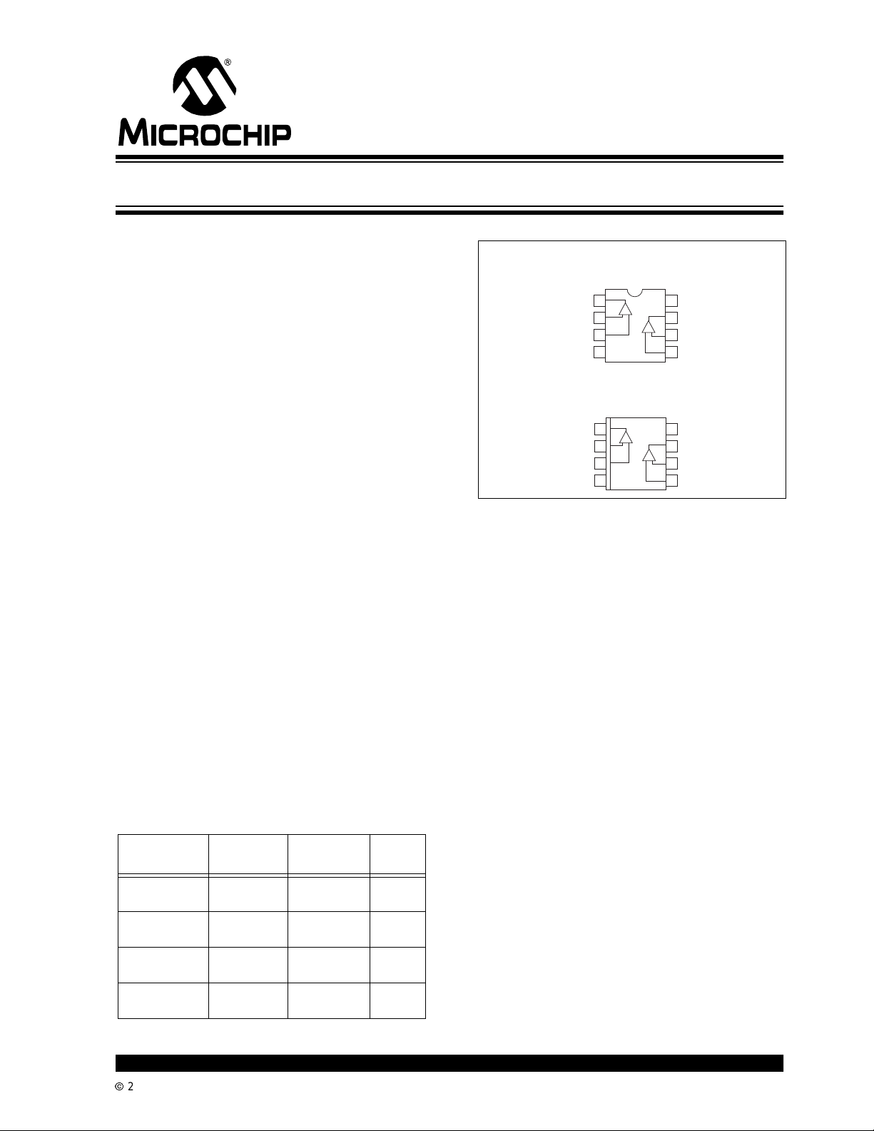
Package Type
PDIP
TC913ACPA
TC913BCPA
-IN A
+IN A
V
SS
1
-
2
3
4
8OUT A
A
+
V
DD
B
OUT B
7
+
-
6
-IN B
+IN B
5
SOIC
TC913ACOA
TC913BCOA
V
8OUT A
DD
B
OUT
7
-
6
-IN B
5
+IN B
-IN A
+IN A
V
1
A
+
-
2
+
3
4
SS
General Description
The TC913 is the world's first complete monolithic,dual
auto-zeroed operational amplifier. The TC913 sets a
new standard for low power, precision dual-operational
amplifiers. Chopper-stabilized or auto-zeroed amplifiers offer low offset voltage errors by periodically sampling offset error, and storing correction voltages on
capacitors. Previous single amplifier designs required
two user-supplied,external 0.1µF error storage correction capacitors — much too large for on- chip integration. The unique TC913 architecture requires smaller
capacitors, making on-chip integration possible.
Microvolt offset levels are achieved and external
capacitors are not required.
The TC913 system benefits are apparent when contrasted with a TC7650 chopper amplifier circuit implementation.A single TC913 replaces two TC7650's and
four capacitors. Five components and assembly steps
are eliminated.
The TC913 pinout matches many popular dual-operationalamplifiers:OP-04, TLC322, LM358, and ICL7621
are typical examples. In many applications, operating
from dual 5V power supplies or single supplies, the
TC913 offers superior electrical performance, and can
be a functional drop-in r eplacement; printed circuit
board rework is not necessary. The TC913's low offset
voltage error eliminates offset voltage trim
potentiometers often needed with bipolar and low
accuracy CMOS operational amplifiers.
The TC913 takes full advantage of Microchip's
proprietary CMOS technology. Unity gain bandwidth is
1.5MHz and slew rate is 2.5V/µsec.
2002 Microchip TechnologyInc. DS21482B-page 1
Page 2
TC913A/TC913B
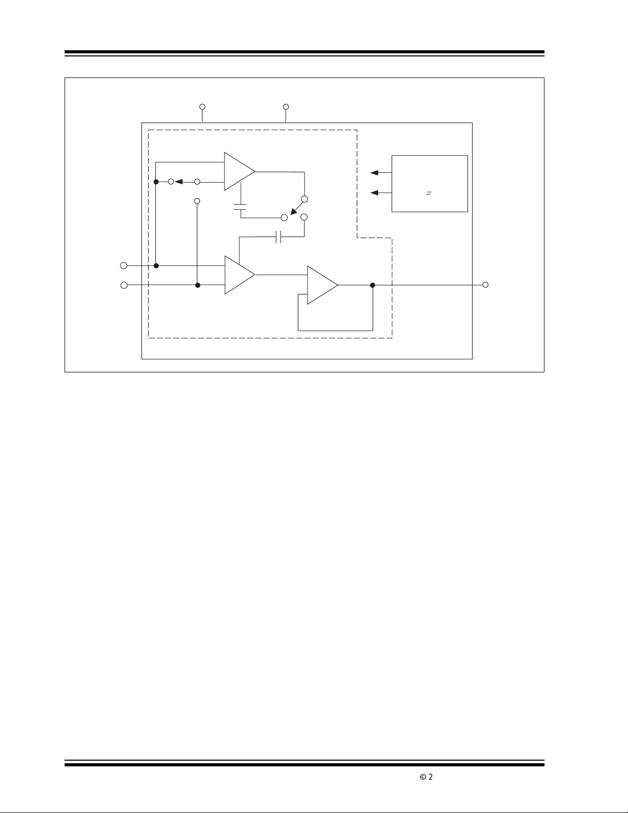
Functional Block Diagram
-Input A
-Input B
+Input A
+Input B
V
SS
48
V
DD
TC913
VOS Correction Amplifier
+
A
–
*
B
A
B
*
Low Impedance
2
6
5
3
1 of 2 Amplifier Shown
*NOTE: Internal capacitors. No external capacitors required.
-
+
Main Amplifier
Output Buffer
+
-
Internal
Oscillator
(f
OSC
200Hz)
1
7
Output A
Output B
DS21482B-page 2
2002 Microchip TechnologyInc.
Page 3
TC913A/TC913B
1.0 ELECTRICAL
CHARACTERISTICS
Absolute Maximum Ratings*
Total Supply Voltage (VDDto VSS) .......................+18V
Input Voltage...................... (V
+0.3V)to (V
DD
SS
-
0.3V)
*Stresses above those listed under "Absolute Maximum
Ratings" may cause permanent damage to the device. These
are stress ratings only and functional operation of the device
at these or any other conditions above those indicated in the
operation sections of the specifications is not implied. Exposure to Absolute Maximum R ating conditions for extended
periodsmay affectdevice reliability.
Current Into Any Pin............................................10mA
While Operating..........................................100µA
Package Power Dissipation (T
–70°C)
A
Plastic DIP ................................................730mW
Plastic SOIC .............................................470mW
Operating Temperature Range
C Device .......................................... 0°C to +70°C
StorageTemperature Range..............-65°C to +150°C
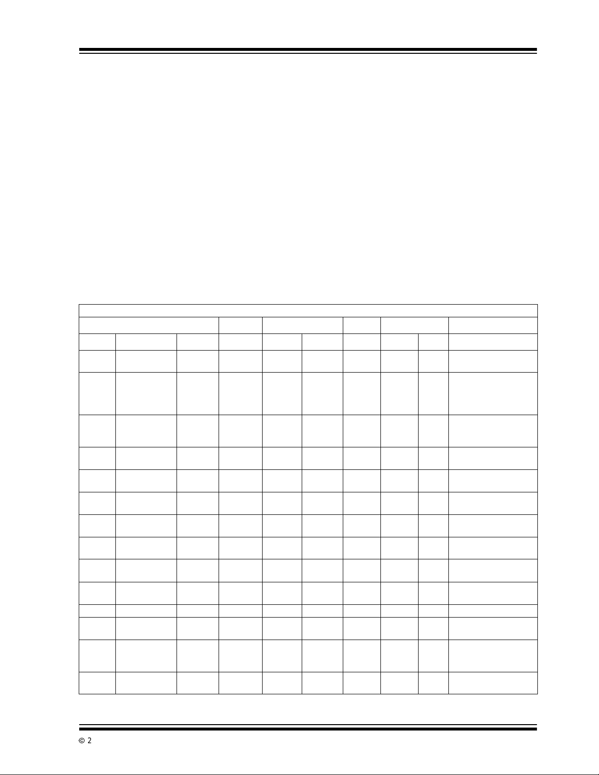
TC913A AND TC913B ELECTRICAL SPECIFICATIONS
Electrical Characteristics: VS=±5V,TA= +25°C, unless otherwise indicated.
TC913A TC913B
Symbol Parameter Min Typ Max Min Typ Max Unit Test Conditions
Input Offset
V
OS
Voltage
TCV
Average Temp.
OS
Coefficient of
Input Offset
Voltage
Average Input
I
B
Bias Current
Average Input
I
OS
Offset Current
Input Voltage
e
N
Noise
CMRR Common Mode
Rejection Ratio
CMVR Common Mode
Voltage Range
Open-Loop
A
OL
Voltage Gain
OUT
OutputVoltage
Swing
V
BW Closed Loop
Bandwidth
SR Slew Rate — 2.5 — — 2.5 — V/µsec R
PSRR Power Supply
Rejection Ratio
Operating
V
S
Supply Voltage
Range
I
Quiescent
S
Supply Current
Note 1: Characterized; not 100% tested.
—515—1530µVTA=+25°C
—
—
0.05
0.05
0.15
0.15
—
—
0.1
0.1
0.25
0.25
µV/°C
µV/°C
0°C ≤ T
-25°C ≤ T
≤ +70°C
A
≤ +85°C
A
(Note 1)
T
—
—
—
—
—
—
—
—
—
—
5
—
0.6
11
90
3
4
20
1
—
—
—
—
—
—
—
—
—
—
—
—
10
—
0.6
11
120
4
6
40
1
—
—
110 116 — 100 110 — dB V
V
SS —
2V
DD -
SS —
V
DD -
V
115 120 — 110 120 — dB RL=10kΩ,V
pA
nA
nA
pAnATA=+25°C
µV
P-P
µV
P-P
2V
=+25°C
A
0°C ≤ T
-25°C ≤ T
T
=+85°C
A
≤ +70°C
A
≤ +85°
A
0.1to1Hz,RS≤ 100Ω
0.1to10Hz,R
≤ VCM≤ VDD-2.2
SS
OUT
VSS+0.3 — VDD-0.9 VSS+0.3 — VDD-0.9 V RL=10kΩ
— 1.5 — — 1.5 — MHz ClosedLoopGain=+1
=10kΩ,CL=50pF
L
110 — — 100 — — dB ±3.3V to ±5.5V
±3.3
6.5
—
—
±8.3
16
±3.3
6.5
—
—
±8.3
16
VVSplit Supply
Single Supply
— 0.65 0.85 — — 1.1 mA VS=±5V
S
≤ 100Ω
=±4V
2002 Microchip TechnologyInc. DS21482B-page 3
Page 4
TC913A/TC913B
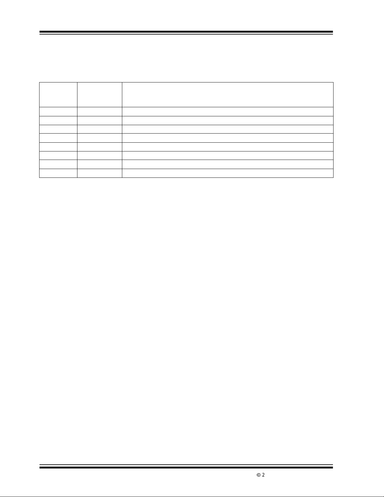
2.0 PIN DESCRIPTIONS
ThedescriptionsofthepinsarelistedinTable2-1.
TABLE 2-1: PIN FUNCTION TABLE
Pin No.
(8-Pin PDIP)
(8-Pin SOIC)
1 OUT A Output
2 -IN A InvertingInput
3 +IN A Non-inverting Input
4V
5 +IN B Non-inverting Input
6 -IN B InvertingInput
7 OUT B Output
8V
Symbol Description
SS
DD
Negative Power Supply
Positive Power Supply
DS21482B-page 4
2002 Microchip TechnologyInc.
Page 5

TC913A/TC913B
3.0 DETAILED DESCRIPTION
3.1 Theory of Operation
Each of the TC913's two Op Amps actually consists of
two amplifiers. A main amplifier is always connected
fromthe inputto the output. A separatenullingamplifier
alternatelynullsits own offset andthen the offsetof the
amplifier. Since each am plifier is continuously being
nulled, offset voltage drift wi th time, temperature and
power supply variations is greatly reduced.
All nulling circuitry is internal and the nulling operation
is transparent to the user. Offset nulling voltages are
stored on two internal capacitors.An internal oscillator
and controllogic,sharedby theTC913'stwoamplifiers,
control the nulling process.
3.2 Pin Compatibility
The TC913 pinout is compatible with OP-14, LM358,
MC1458, LT1013, TLC322, and similar dual Op Amps.
In many circuits operating from single or ±5V supplies,
the TC913 is a drop-in replacement offering DC
performance rivaling that of the best single Op Amps.
The TC913's amplifiers include a low-impedance class
AB output buffer. Some previous CMOS chopper
amplifiers used a high impedance output stage which
made open-loop gain dependent on load resistance.
The TC913's open-loop gain is not dependent on load
resistance.
3.3 Overload Recovery
The TC913 recovers quickly from output saturation.
Typicalrecovery time from positive output saturation is
20 msec. Negative output saturation recovery time is
typically 5 msec.
3.4 Avoiding La tchup
Junction-isolated CMOS circuits inherently contain a
parasitic p-n-p-n transistor circuit. Voltages exceeding
the supplies by 0.3V should not be applied to the
device pins. Lar ger voltages can turn the p-n-p-n
device on, causing excessive device power supply
current and power dissipation. The TC913's power
supplies should be established at the same time or
before input signals are applied. If this is not possible,
input current should be limited to 0.1mA to avoid
triggering the p-n-p-n structure.
2002 Microchip TechnologyInc. DS21482B-page 5
Page 6

TC913A/TC913B
(
g)
4.0 TYPICAL CHARACTERISTICS
Note: The graphs and tables provided following this note are a statistical summary based on a limited number of
samplesandareprovidedforinformational purposesonly. The performance characteristics listed hereinare
not tested or guaranteed. In some graphs or tables, the data presented may be outside the specified
operating range ( e.g., outside specified power supply range) and therefore outside t he warranted range.
Supply Current vs. ± Supply Voltage
1200
TA = +25˚C
1000
800
600
400
SUPPLY CURRENT (µA)
200
0
23 54678
± SUPPLY VOLTAGE (V)
Output Voltage Swing vs.
Load Resistance
T
= +25˚C
A
VS = ±5V
5.0
4.2
3.4
2.6
± OUTPUT VOLTAGE (V)
1.8
1.0
100
1k 10k 100k
LOAD RESISTANCE (Ω)
-SWING
+SWING
Input Offset Voltage vs.
Common Mode Voltage
35
VA = ±5V
30
= +25˚C
T
A
25
20
15
10
INPUT OFFSET VOLTAGE (µV)
5
0
-6
-5 -4 -3 -2 -1 0 1 2 3 4
INPUT COMMON MODE VOLTAGE (V)
Negative Overload Recovery Time
RL = 10 k
= +25˚C
T
A
Gain = –20
1M
HORIZONTAL SCALE = 20 msec/DIV
Ω
INPUT
OUTPUT
= 2 V/DIV
Gain and Phase vs. Frequency
50
40
30
20
10
0
-10
-20
CLOSED-LOOP GAIN (dB)
-30
-40
10k
PHASE
GAIN
100k 1M 10M
FREQUENCY (Hz)
VS = ±5V
= +25˚C
T
A
R
= 10 k
L
225
180
Ω
135
90
45
de
0
PHASE
-45
-90
-135
-180
Positive Overload Recovery Time
OUTPUT =
2 V/DIV
0V
INPUT INPUT
GAIN = –20
HORIZONTAL SCALE = 20 msec/DIV
0V
DS21482B-page 6
2002 Microchip TechnologyInc.
Page 7

5.0 PACKAGING INFORMATION
5.1 Package Marking Information
Package marking data not available at this time.
5.2 Taping Form
Component Taping Orientation for 8-Pin SOIC (Narrow) Devices
User Direction of Feed
PIN 1
TC913A/TC913B
W
P
Standard Reel Component Orientation
for TR Suffix Device
Carrier Tape, Number of Components Per Reel and Reel Size
Package Carrier Width (W) Pitch (P) Part Per Full Reel Reel Size
8-Pin SOIC (N) 12 mm 8 mm 2500 13 in
2002 Microchip TechnologyInc. DS21482B-page 7
Page 8

TC913A/TC913B
.
8
)
)
)
)
)
)
)
)
)
)
)
)
)
)
)
)
8
C
3
)
)
)
)
)
)
)
)
)
)
)
)
)
)
)
)
)
)
)
)
)
)
)
)
8-Pi
P
5.3 Package Dimensions
-Pin SOI
.050 (1.27) TYP
.197 (5.00
.189 (4.80
.020 (0.51
.013 (0.33
n Plastic DI
.157 (3.99
.150 (3.81
.010 (0.25
.004 (0.10
.244 (6.20
.228 (5.79
.069 (1.75
.053 (1.35
.010 (0.25
.007 (0.18
.050 (1.27
.016 (0.40
Dimensions: inches (mm)
.045 (1.14
.030 (0.76
.200 (5.08
.140 (3.56
.150 (3.81
.115 (2.92
.400 (10.16
.348 (8.84
.110 (2.79
.090 (2.29
.070 (1.78
.040 (1.02
.022 (0.56
.015 (0.38
.260 (6.60
.240 (6.10
.040 (1.02
.020 (0.51
.310 (7.87
.290 (7.37
.015 (0.38
.008 (0.20
.400 (10.16
.310 (7.87
Dimensions: inches (mm)
DS21482B-page 8
2002 Microchip TechnologyInc.
Page 9

TC913A/TC913B
SALES AND SUPPORT
Data Sheets
Products supportedby a preliminaryData Sheet may have an errata sheet describing minor operational differences and recommendedworkarounds.To determine if an errata sheet exists for a particulardevice, please contactone of the following:
1. Your local Microchip sales office
2. The Microchip CorporateLiterature Center U.S. FAX: (480)792-7277
3. The Microchip Worldwide Site (www.microchip.com)
Pleasespecify which device, revision of silicon and Data Sheet (includeLiterature #) you are using.
New Customer Notification System
Register on our web site (www.microchip.com/cn) to receive the mostcurrenti nformationon our products.
2002 Microchip TechnologyInc. DS21482B-page 9
Page 10

TC913A/TC913B
NOTES:
DS21482B-page 10
2002 Microchip TechnologyInc.
Page 11

TC913A/TC913B
Information contained in this publication regarding device
applications and the like is intended through suggestion only
and may be superseded by updates. It is your responsibility to
ensure that your application meets with your specifications.
No representation or warranty is given and no liability is
assumed by Microchip Technology Incorporated with respect
to the accuracy or use of such information,or infringement of
patents or other intellectual property rights arising from such
use or otherwise. Use of Microchip’s products as critical components in life support systems is not authorized except with
express written approval by Microchip. No licenses are conveyed, implicitly or otherwise, under any intellectual property
rights.
Trademarks
The Microchip name and logo, the Mi c r ochip logo, FilterLab,
K
EELOQ,microID,MPLAB,PIC,PICmicro,PICMASTER,
PICSTART, PRO MATE, SEEV A L and The Embedded Control
SolutionsCompany areregiste red trademarksof MicrochipTechnologyIncorp or ated in the U.S.A. and other countries.
dsPIC, ECONOMONITOR, Fa nSens e, FlexROM, fuzzyLAB,
In-Circuit Serial Programming, ICSP, ICEPIC, microPort,
Migratable Memory, MPASM, MPLIB, MPLINK, MPSIM,
MXDEV, PICC, PICDEM, PICDEM.net, rfPIC, Select Mode
and Total Enduranceare trademarksof MicrochipTechnology
Incorporated in the U.S.A.
Serialized Quick Turn Programming (SQTP) is a service mark
of Microchip Technology Incorporated in the U.S.A.
All other trademarks mentioned herein are property of their
respective companies.
© 2002, Microchip Technology Incorporated, Printed in the
U.S.A., All Rights Reserved.
Printed on recycled paper.
Microchip received QS-9000 quality system
certification for its worldwide headquarters,
design and wafer fabrication facilities in
Chandler and Tempe, Arizona in July 1999
and Mountain View, California in March 2002.
The Company’s quality system processes and
procedures are QS-9000 compliant for its
®
PICmicro
devices, Serial EEPROMs, microperipherals,
non-volatile memory and analog products. In
addition, Microchip’s quality system for the
design and manufacture of development
systemsisISO 9001certified.
2002 Microchip TechnologyInc. DS21482B-page 11
8-bit MCUs, KEELOQ®code hopping
Page 12

WORLDWIDE SALES AND SERVICE
AMERICAS
Corporate Office
2355 West Chandler Blvd.
Chandler, AZ 85224-6199
Tel: 480-792-7200 Fax: 480-792-7277
Technical Support: 480-792-7627
Web Address: http://www.microchip.com
Rocky Mountain
2355 West Chandler Blvd.
Chandler, AZ 85224-6199
Tel: 480-792-7966 Fax: 480-792-7456
Atlanta
500 Sugar Mill Road, Suite 200B
Atlanta, GA 30350
Tel: 770-640-0034 Fax: 770-640-0307
Boston
2 Lan Drive, Suite 120
Westford, MA 01886
Tel: 978-692-3848 Fax: 978-692-3821
Chicago
333 Pierce Road, Suite 180
Itasca, IL 60143
Tel: 630-285-0071 Fax: 630-285-0075
Dallas
4570 Westgrove Drive, Suite 160
Addison, TX 75001
Tel: 972-818-7423 Fax: 972-818-2924
Detroit
Tri-Atria Office Building
32255 Northwestern Highway, Suite 190
Farmington Hills, MI 48334
Tel: 248-538-2250 Fax: 248-538-2260
Kokomo
2767 S. Albright Road
Kokomo, Indiana 46902
Tel: 765-864-8360 Fax: 765-864-8387
Los Angeles
18201 Von Karman, Suite 1090
Irvine, CA 92612
Tel: 949-263-1888 Fax: 949-263-1338
New York
150 Motor Parkway, Suite 202
Hauppauge, NY 11788
Tel: 631-273-5305 Fax: 631-273-5335
San Jose
Microchip Technology Inc.
2107 North First Street, Suite 590
San Jose, CA 95131
Tel: 408-436-7950 Fax: 408-436-7955
Toronto
6285 Northam Drive, Suite 108
Mississauga, Ontario L4V 1X5, Canada
Tel: 905-673-0699 Fax: 905-673-6509
ASIA/PACIFIC
Australia
Microchip Technology Australia Pty Ltd
Suite 22, 41 Rawson Street
Epping 2121, NSW
Australia
Tel: 61-2-9868-6733 Fax: 61-2-9868-6755
China - Beijing
Microchip Technology Consulting (Shanghai)
Co., Ltd., Beijing Liaison Office
Unit 915
Bei Hai Wan Tai Bldg.
No. 6 Chaoyangmen Beidajie
Beijing, 100027, No. China
Tel: 86-10-85282100 Fax: 86-10-85282104
China - Chengdu
Microchip Technology Consulting (Shanghai)
Co., Ltd., Chengdu Liaison Office
Rm. 2401, 24th Floor,
Ming Xing Financial Tower
No. 88 TIDU Street
Chengdu 610016, China
Tel: 86-28-86766200 Fax: 86-28-86766599
China - Fuzhou
Microchip Technology Consulting (Shanghai)
Co., Ltd., Fuzhou Liaison Office
Unit 28F, World Trade Plaza
No. 71 Wusi Road
Fuzhou 350001, China
Tel: 86-591-7503506 Fax: 86-591-7503521
China - Shanghai
Microchip Technology Consulting (Shanghai)
Co., Ltd.
Room 701, Bldg. B
Far East International Plaza
No. 317 Xian Xia Road
Shanghai, 200051
Tel: 86-21-6275-5700 Fax: 86-21-6275-5060
China - Shenzhen
Microchip Technology Consulting (Shanghai)
Co., Ltd., Shenzhen Liaison Office
Rm. 1315, 13/F , Shenzhen Kerry Centre,
Renminnan Lu
Shenzhen 518001, China
Tel: 86-755-2350361 Fax: 86-755-2366086
China - Hong Kong SAR
Microchip Technology Hongkong Ltd.
Unit 901-6, Tower 2, Metroplaza
223 Hing Fong Road
Kwai Fong, N.T., Hong Kong
Tel: 852-2401-1200 Fax: 852-2401-3431
India
Microchip Technology Inc.
India Liaison Office
Divyasree Chambers
1 Floor, Wing A (A3/A4)
No. 11, O’Shaugnessey Road
Bangalore, 560 025, India
Tel: 91-80-2290061 Fax: 91-80-2290062
Japan
Microchip Technology Japan K.K.
Benex S-1 6F
3-18-20, Shinyokohama
Kohoku-Ku, Yokohama-shi
Kanagawa, 222-0033, Japan
Tel: 81-45-471- 6166 Fax: 81-45-471-6122
Korea
Microchip Technology Korea
168-1, Youngbo Bldg. 3 Floor
Samsung-Dong, Kangnam-Ku
Seoul, Korea 135-882
Tel: 82-2-554-7200 Fax: 82-2-558-5934
Singapore
Microchip Technology Singapore Pte Ltd.
200 Middle Road
#07-02 Prime Centre
Singapore, 188980
Tel: 65-6334-8870 Fax: 65-6334-8850
Taiwan
Microchip Technology Taiwan
11F-3, No. 207
Tung Hua North Road
Taipei, 105, Taiwan
Tel: 886-2-2717-7175 Fax: 886-2-2545-0139
EUROPE
Denmark
Microchip Technology Nordic ApS
Regus Business Centre
Lautrup hoj 1-3
Ballerup DK-2750 Denmark
Tel: 45 4420 9895 Fax: 45 4420 9910
France
Microchip Technology SARL
Parc d’Activite du Moulin de Massy
43 Rue du Saule Trapu
Batiment A - ler Etage
91300 Massy, France
Tel: 33-1-69-53-63-20 Fax: 33-1-69-30-90-79
Germany
Microchip Technology GmbH
Gustav-Heinemann Ring 125
D-81739 Munich, Germany
Tel: 49-89-627-144 0 Fax: 49-89-627-144-44
Italy
Microchip Technology SRL
Centro Direzionale Colleoni
Palazzo Taurus 1 V. Le Colleoni 1
20041 Agrate Brianza
Milan, Italy
Tel: 39-039-65791-1 Fax: 39-039-6899883
United Kingdom
Microchip Ltd.
505 Eskdale Road
Winnersh Triangle
Wokingham
Berkshire,England RG415TU
Tel: 44 118 921 5869 Fax: 44-118 921-5820
04/20/02
DS21482B-page 12
*DS21482B*
2002 Microchip Technology Inc.
 Loading...