

Page 1
M
Charge Pump DC-to-DC Converter
TC7662A
Features
• Wide Operating Range
- 3V to 18V
• Increased Output Current (40mA)
• Pin Compatible with ICL7662/SI7661/TC7660/
LTC1044
• No External Diodes Required
• Low Output Impedance @ I
-40Ω Typ.
• No Low-Voltage Terminal Required
• CMOS Construction
• Available in 8-Pin PDIP and 8-Pin CERDIP
Packages
= 20mA
L
Applications
• Laptop Computers
• Disk Drives
• Process Instrumentation
• µP-based Controllers
Device Selection Table
Part
Number
TC7662ACPA 8-Pin PDIP 0°C to +70°C
TC7662AEPA 8-Pin PDIP -40°C to +85°C
TC7662AIJA 8-Pin CERDIP -25°C to +85°C
TC7662AMJA 8-Pin CERDIP -55°C to +125°C
Package
Operating
Temp.
Range
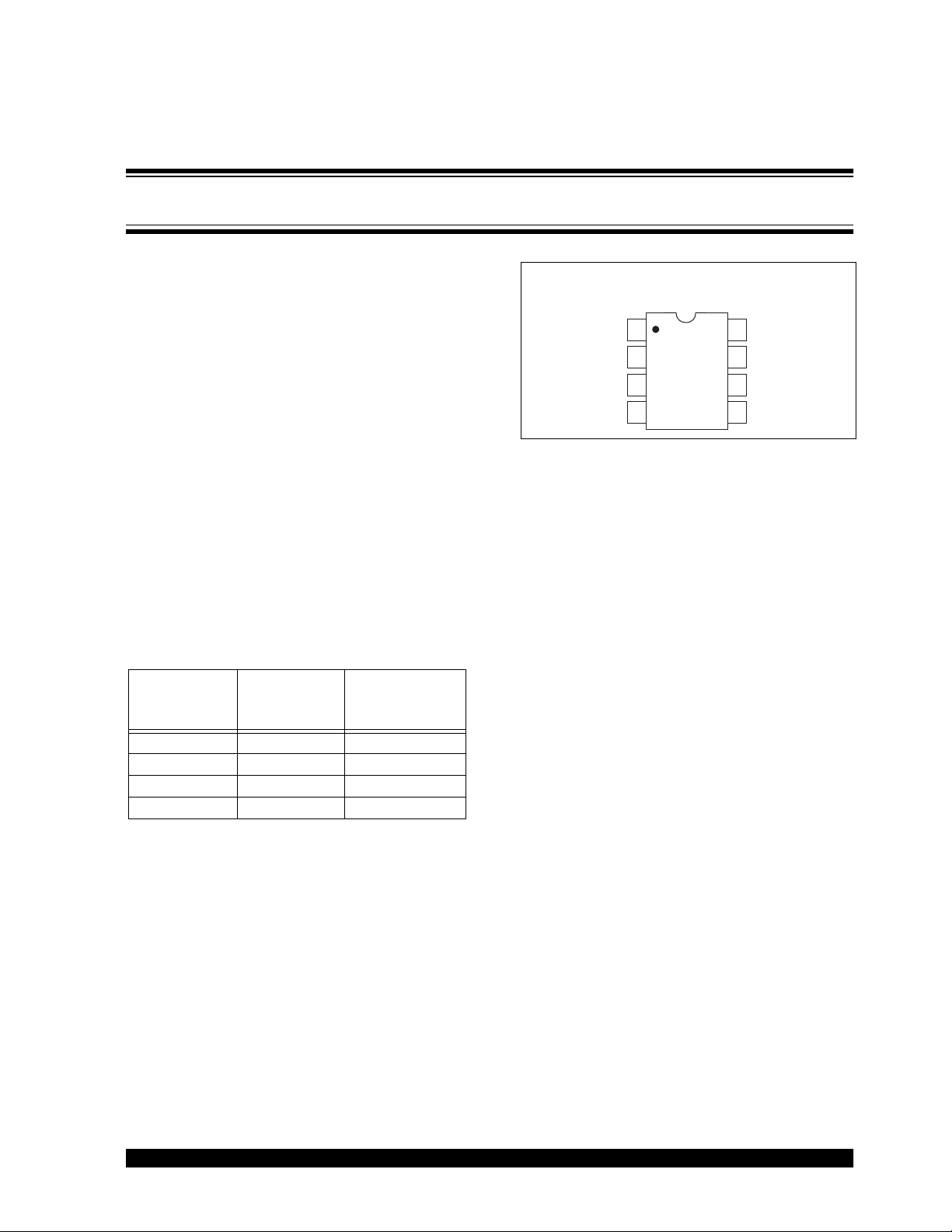
Package Type
8-Pin PDIP
8-Pin CERDIP
NC
C
1
+
2
8
V
DD
7
OSC
TC7662A
GND
C
3
–
4
6
NC
V
5
OUT
General Description
The TC7662A is a pin-compatible upgrade to the
industry standard TC7660 charge pump voltage
converter. It converts a +3V to +18V input to a
corresponding -3V to -18V output using only two lowcost capacitors, eliminating inductors and their
associated cost, size and EMI. In addition to a wider
power supply input range (3V to 18V versus 1.5V to
10V for the TC7660), the TC7662A can source output
currents as high as 40mA. The on-board oscillator
operates at a nominal frequency of 12kHz. Operation
below 12kHz (for lower supply current applications) is
also possible by connecting an ex tern al ca pacitor from
OSC to ground.
The TC7662A directly is recommended for designs
requiring greater output current and/or lower input/
output voltage drop. It is available in 8-pin PDIP and
CERDIP packages in commercial and extended
temperature ranges.
2002 Microchip Technology Inc. DS21468B-page 1
Page 2
TC7662A
Functional Block Diagram
+
–
DS21468B-page 2 2002 Microchip Technology Inc.
Page 3
TC7662A
1.0 ELECTRICAL
CHARACTERISTICS
Absolute Maximum Ratings*
Supply Voltage VDD to GND.................................+18V
Input Voltage (Any Pin).........(V
+ 0.3) to (V
DD
SS
– 0.3)
Stresses above those listed under "Absolute Maximum
Ratings" may cause permanent damage to the device. These
are stress ratings only and functional operation of the device
at these or any other conditions above those indicated in the
operation sections of the specifications is not implied.
Exposure to Absolute Maximum Rating conditions for
extended periods may affect device reliability.
Current into Any Pin............................................10mA
Output Short Circuit ........... Continuous (at 5.5V Input)
ESD Protection ................................................±2000V
Package Power Dissipation (T
≤ 70°C)
A
8-Pin CERDIP..........................................800mW
8-Pin PDIP...............................................730mW
Package Thermal Resistance
CPA, EPA θ
IJA, MJA θ
.........................................140°C/W
JA
............................................90°C/W
JA
Operating Temperature Range
C Suffix............................................0°C to +70°C
I Suffix..........................................-25°C to +85°C
E Suffix.........................................-40°C to +85°C
M Suffix......................................-55°C to +125°C
Storage Temperature Range..............-65°C to +150°C
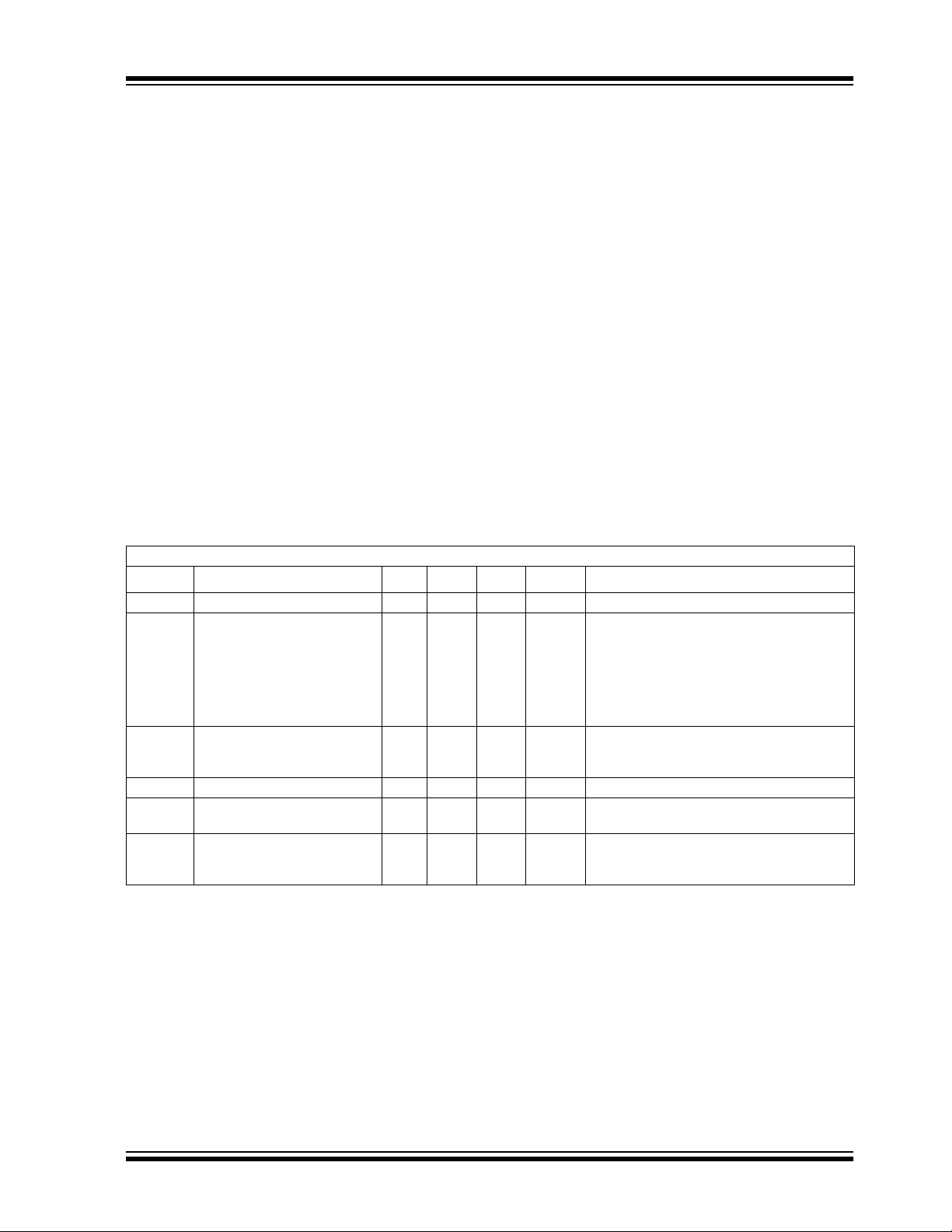
TC7662A ELECTRICAL SPECIFICATIONS
Electrical Characteristics: VDD = 15V, TA = +25°C, Test circuit (Figure 3- 1) unless otherw ise noted.
Symbol Parameter Min Typ Max Units Test Conditions
V
I
R
F
P
V
DD
S
O
OSC
EFF
EFF
Supply Voltage 3 — 18 V
Supply Current —
—
—
—
—
—
—
Output Source Resistance —
—
—
Oscillator Frequency — 12 — kHz
Power Efficiency 93
—
Voltage Efficiency 99
—
96
—
510
560
650
190
210
210
40
50
100
97
—
99.9
—
—
—
700
—
—
—
—
—
50
60
125
—
—
—
—
—
µAR
Ω I
%VDD = +15V
%VDD = +15V
= ∞
L
VDD = +15V
0
°C ≤ T
≤ +70°C
A
≤ T
= +5V
≤ T
= 2kΩ
= ∞
≤ +125°C
A
≤ +70°C
A
≤ +125°C
A
-55°C
V
DD
0
°C ≤ T
-55°C
= 20mA, VDD = +15V
L
I
= 40mA, VDD = +15V
L
= 3mA, VDD = +5V
I
L
R
L
R
L
Over operating temperature range.
2002 Microchip Technology Inc. DS21468B-page 3
Page 4
TC7662A
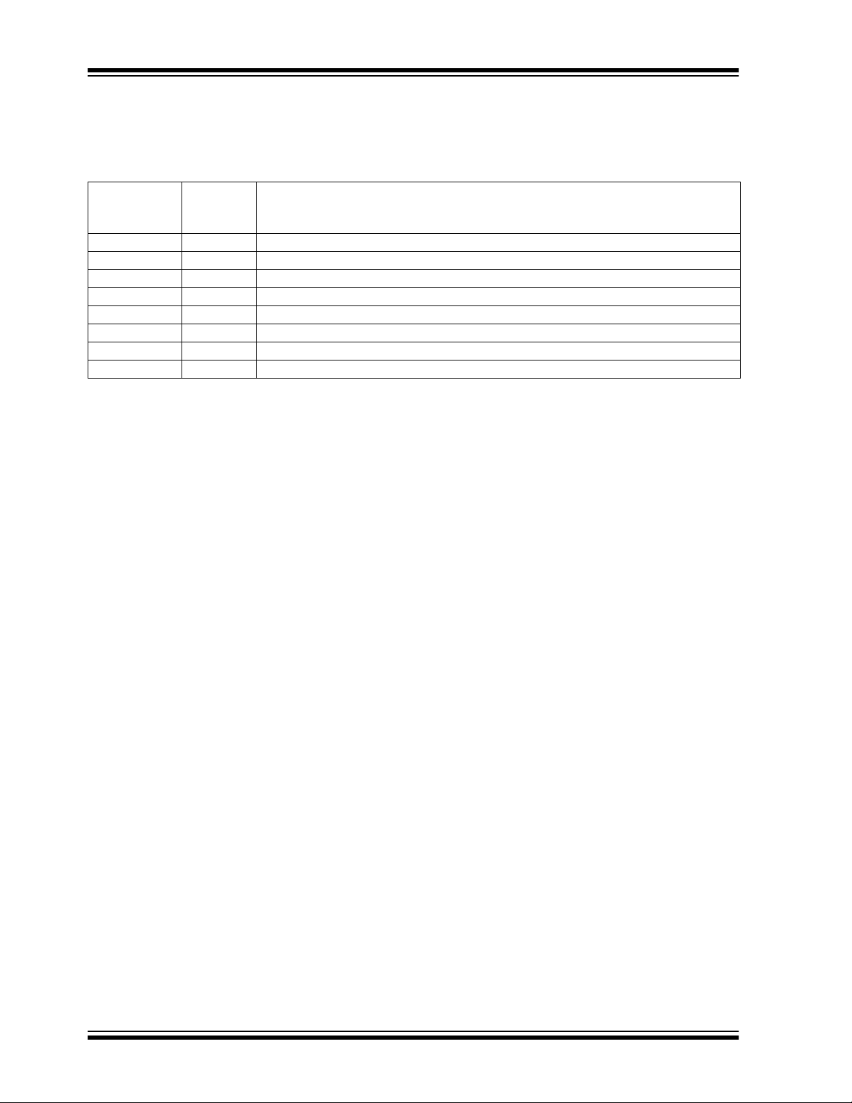
2.0 PIN DESCRIPTIONS
The descriptions of the pins are listed in Table 2-1.
TABLE 2-1: PIN FUNCTION TABLE
Pin No.
(8-Pin PDIP,
CERDIP)
1 NC No connection.
2C
3 GND Ground terminal.
4C
5V
6 NC No connection.
7 OSC Oscillator control input. Bypass with an external capacitor to slow the oscillator.
8V
Symbol Description
+
Charge pump capacitor positive terminal.
-
Charge pump capacitor negative terminal.
OUT
DD
Output voltage.
Power supply positive voltage input.
DS21468B-page 4 2002 Microchip Technology Inc.
Page 5
TC7662A
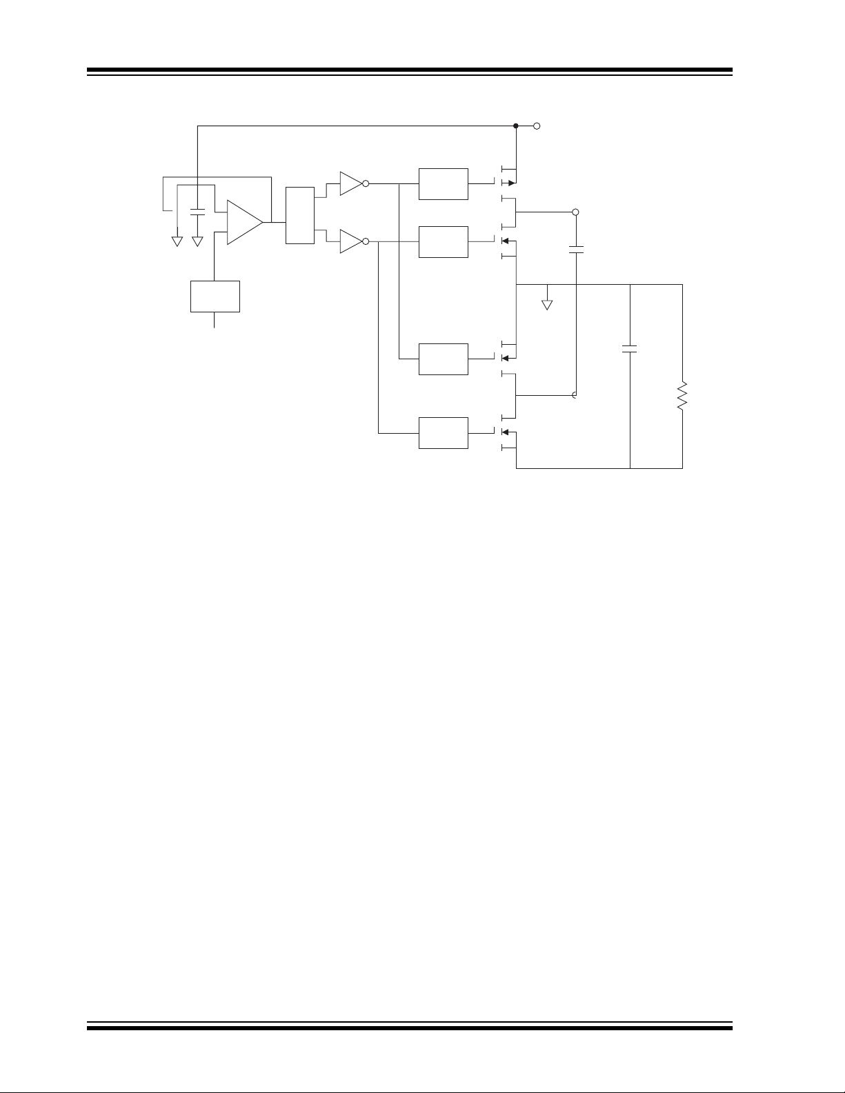
3.0 DETAILED DESCRIPTION
The TC7662A is a c apac itive ch arge pump (sometime s
called a switched-capacitor circuit), where four
MOSFET switches con trol th e cha rge and disc harge of
a capacitor.
The functional block diag ram sho ws how the switc hin g
action works. SW1 and SW2 are turned on simultaneously, charging C
assumes that th e ON resistance of the MOSFETs in
series with the capacitor produce a charging time
(3 time constants) less than the ON time provided by
the oscillator frequency, as shown:
3 (R
DS(ON) CP
In the next cycle, SW1 and SW2 are turned OFF and,
after a very short interval with all switches OFF
(preventing large currents from occurring due to cross
conduction), SW3 and SW4 are turn ed ON. The charge
is then transferred to CR, but with the polarity
in C
P
inverted. In this way, a negative voltage is derived.
An oscillator supplies pulses to a flip-flop that is fed to
a set of level shifters. These level shifters then drive
each set of switches at one-half the oscillator
frequency.
The oscillator has a pin that controls the frequency
of oscillation. Pin 7 can have a capacitor added that
is connected to ground. This will lower the frequency
of the oscillator by adding capacitance to the
internal timing capacitor of the TC7662A. (See Typical
Characteristics – Oscillator Frequency vs. C
FIGURE 3-1: TC7662A TEST CIRCUIT
NC
+
10µF
C
P
to the su pply vol tage, VDD. This
P
) <CP/(0.5 f
1
2
TC7662A
3
4
OSC
8
7
6
5
NC
).
C
OSC
.)
OSC
I
S
V
DD
(+5V)
I
L
R
L
V
OUT
(-5V)
C
10µF
R
+
3.1 Theoretical Power Efficiency
Considerations
In theory, a voltage converter can approach 100%
efficiency if cert a in co ndi tio ns are me t:
1. The drive circuitry consumes minimal power.
2. The output switches ha ve extremely low ON
resistance and virtually no offset.
3. The impedances of the pump and reservoir
capacitors are negligible at the pump frequency.
The TC7662A approaches these conditions for
negative voltage conversion if large values of C
are used.
C
R
and
P
Note: Energy is lost only in the transfer of charge
between capacitors if a change in voltage
occurs.
The energy lost is defined by:
2
E = 1/2 C
(V
P
2
– V
1
)
2
V1 and V2 are the volta ges o n CP during the pump and
transfer cycles. If the impedances of C
and CR are
P
relatively high a t the pump fre quency (ref er to Figure 3-
1), compared to the value of R
substantial di fference in voltage s V
it is desirable not only to make C
, there will be a
L
and V2. Therefore,
1
as large as possible
R
to eliminate output voltage ripple, but also to employ a
correspondingly large value for CP in order to achieve
maximum efficiency of operation.
3.2 Dos and Don’ts
• Do not exceed maximum supply voltages.
• Do not short circuit the output to V+ supply for
voltages above 5.5V for extended periods;
however , tran sie nt con di tion s inc lu din g st art-up
are okay.
• When using polarized capacitors in the inverting
mode, the + terminal of C
pin 2 of the TC7662A and the + terminal of C
must be connected to GND (pin 3).
• If the voltage supply driving the TC7662A has a
large source impedance (25-30 ohms), then a
2.2µF capacitor from pin 8 to ground may be
required to limit the rate o f rise of the inpu t volt age
to less than 2V/µsec.
must be connected to
P
R
2002 Microchip Technology Inc. DS21468B-page 5
Page 6

TC7662A
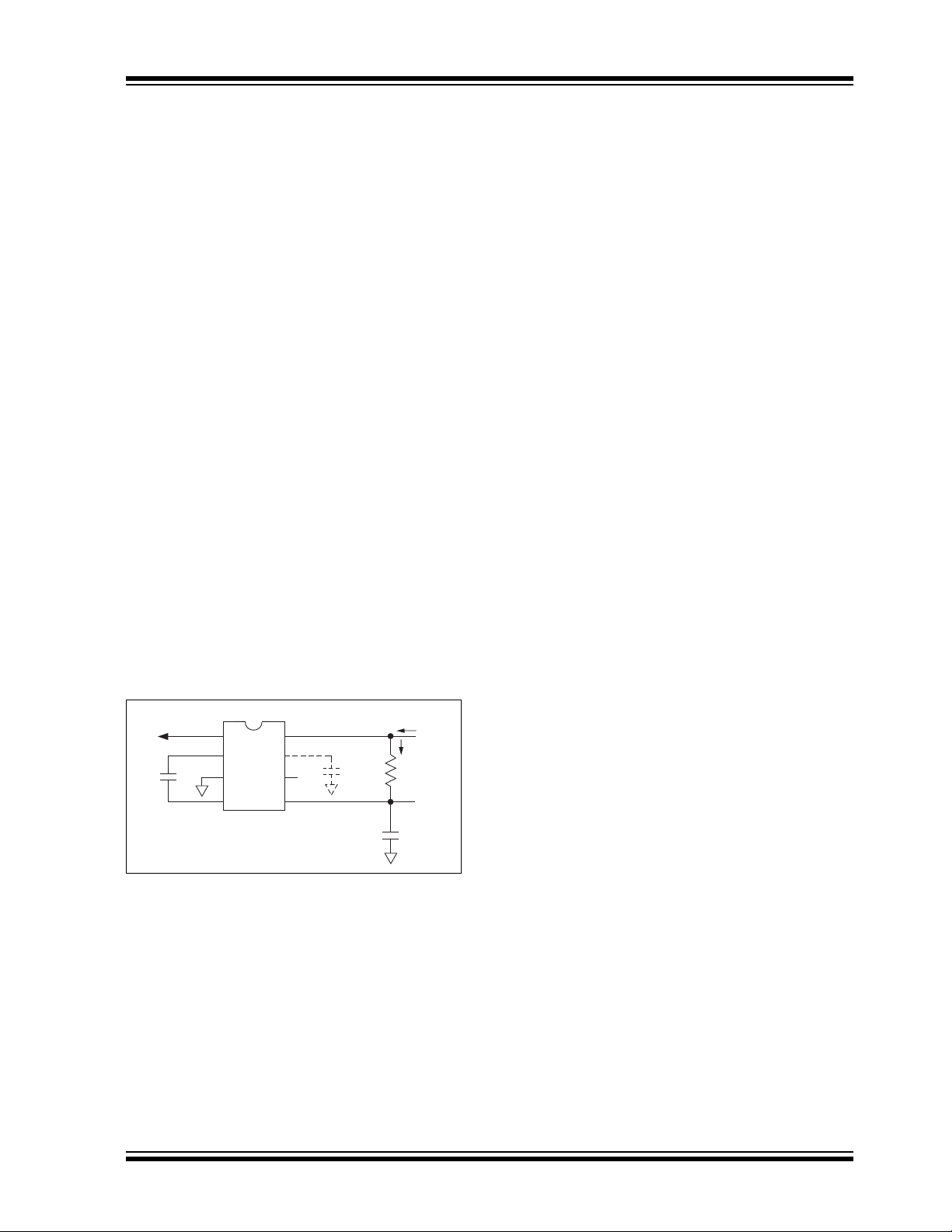
4.0 TYPICAL APPLICATIONS
4.1 Simple Negative Voltage
Converter
The majority of applications will undoubtedly utilize the
TC7662A for generation of negative supply voltages.
Figure 4-1 shows typical connections to provide a
negative supply whe re a positive supply of +3V to +18V
is available.
FIGURE 4-1: SIMPLE NEGATIVE
CONVERTER AND ITS
OUTPUT EQUIVALENT
V
DD
1
2
+
10µF
TC7662A
3
4
The output characteristics of the circuit in Figure 4-1
are those of a nearly ideal volt age sourc e in series with
a resistance as shown in Figure 4-1b. The voltage
source has a value of -(V
) is a function of the ON resistance of the internal
(R
O
MOS switches (shown in the Functional Block
Diagram), the swit ching freque ncy, the value of C
, and the ESR (equivalent series resistance) of C
C
R
and CR. A good first order approximation for RO is:
R
(f
PUMP
O
≅ 2(R
+ R
SW1
ESR
f
OSC
= , R
2
8
7
6
5
10µF
= -V+
V
OUT
–
+
R
O
V
OUT
–
VDDV
V
V
DD
DD
DD
+
AB
). The output impedance
DD
and
P
+ ESRCP) + 2(R
SW2
1
) + + ESR
CP
SWX
x C
f
PUMP
P
= MOSFET switch resistance)
SW3
CR
+ R
SW4
+
Combining the four R
R
≅ 2 x R
O
+ + 4 x ESRCP + ESR
SW
terms as RSW, we see that:
SWX
1
f
x C
PUMP
P
CR
Ω
RSW, the total switch resi st a nc e, is a fun cti on o f supply
voltage and temperature (See Section5.0, Typical
Characteristics “Output Source Resistance” graphs),
typically 23Ω at + 25 °C and 5V. Careful selection of C
P
and CR will reduce the re maining terms, mi nimizin g the
output impedance. High value capacitors will
reduce the 1/(f
x CP) component, and low ESR
PUMP
capacitors will lower the ESR term. Increasing the
oscillator frequenc y will reduce the 1/(f
PUMP
x CP) term,
but may have the side effect of a net increase in output
impedance when CP > 10µF and there is not enough
time to fully charge the capacitors every cycle. In a typical application when f
= 12kHz and C = CP = CR =
OSC
10µF:
R
≅ 2 x 23 + + 4 x ESR
O
(5 x 12
R
O
1
3
x 10 x 10-6)
≅ (46 + 20 + 5 x E S R
+ ESR
CP
)Ω
C
CR
Since the ESRs of the capacitors are reflected in the
output impedance multiplied by a factor of 5, a high
value could potent ially sw amp o ut a low 1/( f
PUMP
x CP)
term, rendering an increase in switching frequency
or filter capacitance ineffective. Typical electrolytic
capacitors may have ESRs as high as 10Ω.
P
DS21468B-page 6 2002 Microchip Technology Inc.
Page 7

TC7662A
4.2 Output Ripple
ESR also affec ts the rip ple volta ge se en at t he ou tp ut.
The total ripple is determined by 2 voltages, A and B,
as shown in Figure 4-2. Segment A is the voltage drop
across the E SR of C
charged by C
P
charged through the load (current flowing out of C
The magnitude of this current change is 2 x I
the total drop is 2 x I
the voltage ch ange acros s C
the cycle when C
drop at B is I
OUT
voltage is the sum of these voltage drops:
V
≅ ( + 2 x ESR
RIPPLE
FIGURE 4-2: OUTPUT RIPPLE
0
V
at the ins tan t it g o es fr om be i ng
R
(current flowing into CR) to being dis-
R
, hence
x ESRCR volts. Segm en t B is
OUT
supplies curr ent to the load. The
R
during time t2, the half of
R
OUT
x t2/CR volts. The peak-to-peak ripple
B
2 x f
PUMP
t
2
1
x C
R
t
1
CR
x I
OUT
)
4.3 Paralleling Devices
Any number of TC7662A voltage converters may be
paralleled to reduce output resistance (Figure 4-3).
The reservoir capacitor, C
each device requires its own pump capacitor, C
, serves all devices, while
R
. The
P
resultant output resistance would be approximately:
).
R
OUT
R
(of TC7662A)
OUT
=
n (number of devices)
4.4 Cascading Devices
The TC7662A may be cascad ed as shown (Figu re 4-4)
to produce larger negative multiplication of the initial
supply voltage. However, due to the finite efficiency of
each device, the practical limit is 10 devices for light
loads. The output voltage is defined by:
= – n (VIN)
V
OUT
where n is an integer representing the number of
devices cascaded. The resulting output resistance
would be approximately the weighted sum of the
individual TC7662A R
OUT
values.
-(VDD)
A
FIGURE 4-3: PARALLELING DEVICES LOWERS OUTPUT IMPEDANCE
V
DD
1
2
C
1
TC7662A
3
4
"1"
8
7
6
5
C
1
1
2
TC7662A
3
4
"n"
8
7
6
5
FIGURE 4-4: INCREASED OUTPUT VOLTAGE BY CASCADING DEVICES
V
DD
10µF
1
2
+
TC7662A
3
4
"1"
8
7
6
5
10µF
+
10µF
1
2
TC7662A
3
4
"n"
8
7
6
5
R
L
C
2
+
V
*
OUT
10µF
+
*V
= -nV
OUT
DD
2002 Microchip Technology Inc. DS21468B-page 7
Page 8

TC7662A
4.5 Changing the TC7662A Oscillator
Frequency
It is possible to increase the conversion efficiency of
the TC7662A at low load levels by lowering the
oscillator freque ncy. This reduces the switching los ses,
and is shown in Figure 4-5. However, lowering the
oscillator freque nc y will cause an undesirable increas e
in the impedance of the pump (C
) and reservoir (CR)
P
capacitors; th is is overco me by increa sing the valu es of
C
and CR by the same factor that the frequency has
P
been reduced. For example, the addition of a 100pF
capacitor between pin 7 (OSC) and V
will lower the
DD
oscillator frequen cy to 2kHz from its nom inal freque ncy
of 12kHz (multiple of 6), and thereby necessitate a
corresponding i ncrease in the value of C
and CR (from
P
10µF to 68µF).
FIGURE 4-5: LOWERING OSCILLATOR
FREQUENCY
V
DD
10µF
1
2
+
TC7662A
3
4
8
7
C
6
5
OSC
V
OUT
10µF
+
4.6 Positive Voltage Doubling
4.7 Combined Negative Voltage
Conversion and Positive Supply
Multiplication
Figure 4-7 com bin es the fu nct ion s shown in Figure 4-1
and Figure 4-6 to pr ovid e negati ve voltag e conve rsion
and positive voltage doubling simultaneously. This
approach would be, for example, suitable for generating +9V and -5V from an existing +5V supply. In this
instance, capacitors C1 and C3 perform the pump and
reservoir functions, respectively, for the generation of
D
1
V
(2 V
D
2
and C4 are
2
V
=
OUT
– V
-(V
DD
C
3
+
=
OUT
) – (2 VF)
DD
+
C
4
)
F
the negative voltage, while capacitors C
pump and reservoir, respectively, for the doubled
positive volta ge. There is a penal ty in this co nfiguratio n
which combines both functions, however, in that the
source impedances of the generated supplies will be
somewhat higher due to the finite impedance of the
common charge pump driver at pin 2 of the device.
FIGURE 4-7: COMBINED NEGATIVE
CONVERTER AND
POSITIVE DOUBLER
V
DD
1
2
TC7662A
3
4
+
C
1
8
7
6
5
+
C
2
The TC7662A may be employed to achieve positive
voltage doubling using the circuit shown in Figure 4-6.
In this application, the pump inverter switches of the
TC7662A are used to charge C
V
– VF (where VDD is the supply voltage and VF is
DD
the forward volta ge on C
applied through dio de D
thus created on C
R
plus the supply volt age (VDD)
P
to capacitor CR). The voltage
2
becomes (2 VDD) – (2 VF), or twice
to a voltage level of
P
the supply volt age minus the combined forward voltage
drops of diodes D
The source impe dance of the o utput (V
on the output current, but for V
and D2.
1
) will depend
OUT
= 5V and an output
DD
current of 10 mA, it will be approximately 60Ω.
FIGURE 4-6: POSITIVE VOLTAGE
MULTIPLIER
V
DD
1
2
TC7662A
3
4
8
D
7
1
6
5
+
C
V
=
OUT
D
2
P
) – (2 VF)
(2 V
DD
+
C
R
4.8 Voltage Splitting
The same bidirectional characteristics can be used to
split a higher supply in half, as shown in Figure 4-8.
The combined load will be evenly shared between the
two sides. Because the switches share the load in
parallel, the output impedance is much lower than in
the standard c ircuit s, and hi gher curren ts ca n be drawn
from the device. By using this circuit, and then the
circuit of Figure 4-4, +15V can be converted (via +7.5V
and -7.5V) to a nominal -15V, though with rather high
series resistance (~ 25 0Ω).
FIGURE 4-8: SPLITTING A SUPPLY IN
HALF
V
DD
R
L1
V
=
OUT
–
V
– V
DD
50
µF
2
R
L2
50µF
+
–
50µF
+
1
–
2
TC7662A
3
4
+
–
8
7
6
5
–
V
DS21468B-page 8 2002 Microchip Technology Inc.
Page 9

TC7662A
00
01001000
0
)
(
)
0
C
OSC
0k
5
C
5.0 TYPICAL CHARACTERISTICS
Note: The graphs and tables provided following this note are a statistical summary based on a limited number of
samples and are pro vided for information al purposes only. The performance characte ristics listed h erein are
not tested or guaranteed. In some graphs or tables, the data presented may be outside the specified
operating range (e.g., outside specified power supply range) and therefore outside the warranted range.
Circuit of Figure 3-1, CP = CR = 10µF, C
Supply Current vs. Temperature
700
600
500
400
300
200
SUPPLY CURRENT (µA)
100
0
-60 -40 -20 0 20 40 60 80 100 120 140
TEMPERATURE (°C)
Frequency vs. Temperature
20
18
16
14
12
10
FREQUENCY (kHz)
8
6
-60 -40 -20 0 20 40 60 80 100 120 140
TEMPERATURE (°C)
ESRCP
VDD = 15V
VDD = 5V
≈ C
≈ 1Ω, TA = 25°C unless otherwise noted.
ESRCR
Oscillator Frequency vs.
1
Hz
REQUENCY
1
1
1
Output Resistance vs. Temperature
160
140
Ω
120
VDD = 5V, IL = 3mA
100
80
60
OUTPUT RESISTANCE ( )
40
20
-60 -40 -20 0 20 40 60 80 100 120 140
= +2
10,00
CAPACITANCE (pF
VDD = 15V, IL = 20mA
TEMPERATURE (°C)
Power Conversion Efficiency vs. I
110
100
90
Efficiency
80
70
60
50
40
30
20
10
POWER CONVERSION EFFICIENCY (%)
16 32 48 64 80
8244056720
LOAD CURRENT (mA)
Supply
Current
T
= +25°C
A
LOAD
165
150
135
120
105
90
75
60
45
SUPPLY CURRENT (mA)
30
15
0
Output Resistance vs. Input Voltage
110
100
90
Ω
80
70
60
50
40
30
OUTPUT RESISTANCE ( )
20
10
0
IL =
20mA
2 6 10 14 18
4 8 12 16 20
INPUT VOLTAGE (V)
TA = +25°C
2002 Microchip Technology Inc. DS21468B-page 9
Page 10

TC7662A
3
)
)
)
)
)
)
)
)
)
)
)
)
)
)
)
)
)
)
)
)
)
)
)
)
6.0 PACKAGING INFORMATION
6.1 Package Marking Information
Package mar k ing data not available a t this time.
6.2 Package Dimensions
.260 (6.60
.240 (6.10
.045 (1.14
.030 (0.76
.200 (5.08
.140 (3.56
.150 (3.81
.115 (2.92
.400 (10.16
.348 (8.84
.110 (2.79
.090 (2.29
.070 (1.78
.040 (1.02
.022 (0.56
.015 (0.38
.040 (1.02
.020 (0.51
.310 (7.87
.290 (7.37
.015 (0.38
.008 (0.20
.400 (10.16
.310 (7.87
DS21468B-page 10 2002 Microchip Technology Inc.
Page 11

TC7662A
Sales and Support
Data Sheets
Products supported by a preliminary Data Sheet may have an errata sheet describing minor operational differences and recommended workarounds. To determine if an errata sheet exists for a particular device, please contact one of the following:
1. Your local Microchip sales office
2. The Microchip Corporate Literature Center U.S. FAX: (480) 792-7277
3. The Microchip Worldwide Site (www.microchip.com)
Please specify which device, revision of silicon and Data Sheet (include Literature #) you are using.
New Customer Notification System
Register on our web site (www.microchip.com/cn) to receive the most current information on our products.
2002 Microchip Technology Inc. DS21468B-page11
Page 12

TC7662A
NOTES:
DS21468B-page12 2002 Microchip Technology Inc.
Page 13

TC7662A
Information contained in this publication regarding device
applications and the like is intended through suggestion only
and may be superseded by updates. It is your responsibility to
ensure that your application meets with your specifications.
No representation or warranty is given and no liability is
assumed by Microchip Technology Incorporated with respect
to the accuracy or use of such information, or infringement of
patents or other intellectual property rights arising from such
use or otherwise. Use of Microchip’s products as critical components in life support systems is not authorized except with
express written approval by Microchip. No licenses are conveyed, implicitly or otherwise, under any intellectual property
rights.
Trademarks
The Microchip name and logo, the Microchip logo, FilterLab,
EELOQ, microID, MPLAB, PIC, PICmicro, PICMASTER,
K
PICSTART, PRO MATE, SEEVAL and The Embedded Co ntrol
Solutions Company are registered trademarks of Microchip Technology Incorporated in the U.S.A. and other countries.
dsPIC, ECONOMONITOR, FanSense, FlexROM, fuzzyLAB,
In-Circuit Serial Programming, ICSP, ICEPIC, microPort,
Migratable Memory, MPASM, MPLIB, MPLINK, MPSIM,
MXDEV, PICC, PICDEM, PICDEM.net, rfPIC, Select Mode
and T otal Endurance are trademarks of Microchip Technology
Incorporated in the U.S.A.
Serialized Quick Turn Programming (SQTP) is a service mark
of Microchip Technology Incorporated in the U.S.A.
All other trademarks mentioned herein are property of their
respective companies.
© 2002, Microchip Technology Incorporated, Printed in the
U.S.A., All Rights Reserved.
Printed on recycled paper.
Microchip received QS-9000 quality system
certification for its worldwide headquarters,
design and wafer fabrication facilities in
Chandler and Tempe, Arizona in July 1999
and Mountain View, California in March 2002.
The Company’s quality system processes and
procedures are QS-9000 compliant for its
PICmicro
devices, Serial EEPROMs, micrope ri ph era ls,
non-volatile memory and ana l og pro duc ts. In
addition, Microchip’s quality system for the
design and manufacture of development
systems is ISO 9001 certified.
®
8-bit MCUs, KEELOQ
®
code hoppin g
2002 Microchip Technology Inc. DS21468B-page 13
Page 14

M
WORLDWIDE SALES AND SERVICE
AMERICAS
Corporate Office
2355 West Chandler Blvd.
Chandler, AZ 85224-6199
Tel: 480-792-7200 Fax: 480-792-7277
Technical Support: 480-792-7627
Web Address: http://www.microchip.com
Rocky Mountain
2355 West Chandler Blvd.
Chandler, AZ 85224-6199
Tel: 480-792-7966 Fax: 480-792-7456
Atlanta
500 Sugar Mill Road, Suite 200B
Atlanta, GA 30350
Tel: 770-640-0034 Fax: 770-640 -03 07
Boston
2 Lan Drive, Suite 120
Westford, MA 01886
Tel: 978-692-3848 Fax: 978-692 -38 21
Chicago
333 Pierce Road, Suite 180
Itasca, IL 60143
Tel: 630-285-0071 Fax: 630-285-0075
Dallas
4570 Westgrove Drive, Suite 160
Addison, TX 75001
Tel: 972-818-7423 Fax: 972-818 -29 24
Detroit
Tri-Atria Office Building
32255 Northwestern Highway, Suite 190
Farmington Hills, MI 48334
Tel: 248-538-2250 Fax: 248-538-2260
Kokomo
2767 S. Albright Road
Kokomo, Indiana 46902
Tel: 765-864-8360 Fax: 765-864-8387
Los Angeles
18201 Von Karman, Suite 1090
Irvine, CA 92612
Tel: 949-263-1888 Fax: 949-263 -13 38
New York
150 Motor Parkway, Suite 202
Hauppauge, NY 11788
Tel: 631-273-5305 Fax: 631-273 -53 35
San Jose
Microchip Technology Inc.
2107 North First Street, Suite 590
San Jose, CA 95131
Tel: 408-436-7950 Fax: 408-436 -79 55
Toronto
6285 Northam Drive, Suite 108
Mississauga, Ontario L4V 1X5, Cana da
Tel: 905-673-0699 Fax: 905-673-6509
ASIA/PACIFIC
Australia
Microchip Technology Australia Pty Ltd
Suite 22, 41 Rawson Street
Epping 2121, NSW
Australia
Tel: 61-2-9868-6733 Fax: 61-2-9868-6755
China - Beij ing
Microchip Technology Consulting (Shanghai)
Co., Ltd., Beijing Liaison Office
Unit 915
Bei Hai Wan Tai Bldg.
No. 6 Chaoyangmen Beidajie
Beijing, 100027, No. China
Tel: 86-10-85282100 Fax: 86-10-85282104
China - Chengdu
Microchip Technology Consulting (Shanghai)
Co., Ltd., Chengdu Liaison Office
Rm. 2401, 24th Floor,
Ming Xing Financial Tower
No. 88 TIDU Street
Chengdu 610016, China
Tel: 86-28-6766200 Fax: 86-28-6766599
China - Fuzhou
Microchip Technology Consulting (Shanghai)
Co., Ltd., Fuzhou Liaison Office
Unit 28F, World Trade Plaza
No. 71 Wusi Road
Fuzhou 350001, China
Tel: 86-591-7503506 Fax: 86-591-7503521
China - Shanghai
Microchip Technology Consulting (Shanghai)
Co., Ltd.
Room 701, Bldg. B
Far East International Plaza
No. 317 Xian Xia Road
Shanghai, 200051
Tel: 86-21-6275-5700 Fax: 86-21-6275-5060
China - Shenzhen
Microchip Technology Consulting (Shanghai)
Co., Ltd., Shenzhen Liaison Office
Rm. 1315, 13/F, Shenzhen Kerry Centre,
Renminnan Lu
Shenzhen 518001, China
Tel: 86-755-2350361 Fax: 86-755-2366086
Hong Kong
Microchip Technology Hongkong Ltd.
Unit 901-6, Tower 2, Metroplaza
223 Hing Fong Road
Kwai Fong, N.T., Hong Kong
Tel: 852-2401-1200 Fax: 852-2401-3431
India
Microchip Technology Inc.
India Liaison Office
Divyasree Chambers
1 Floor, Wing A (A3/A4)
No. 11, O’Shaugnessey Road
Bangalore, 560 025, India
Tel: 91-80-2290061 Fax: 91-80-2290062
Japan
Microchip Technology Japan K.K.
Benex S-1 6F
3-18-20, Shinyokohama
Kohoku-Ku, Yokohama-shi
Kanagawa, 222-0033, Japan
Tel: 81-45-471- 6166 Fax: 81-45-471-6122
Korea
Microchip Technology Korea
168-1, Youngbo Bldg. 3 Floor
Samsung-Dong, Kangnam-Ku
Seoul, Korea 135-882
Tel: 82-2-554-7200 Fax: 82-2-558-5934
Singapore
Microchip Technology Singapore Pte Ltd.
200 Middle Road
#07-02 Prime Centre
Singapore, 188980
Tel: 65-6334-8870 Fax: 65-6334-8850
Taiwan
Microchip Technology Taiwan
11F-3 , No . 207
Tung Hua North Road
Taipei, 105, Taiwan
Tel: 886-2-2717-7175 Fax: 886-2-2545-0139
EUROPE
Denmark
Microchip Technology Nordic ApS
Regus Business Centre
Lautrup hoj 1-3
Ballerup DK-2750 Denmark
Tel: 45 4420 9895 Fax: 45 4420 9910
France
Microchip Technology SARL
Parc d’Activite du Moulin de Massy
43 Rue du Saule Trapu
Batiment A - ler Etage
91300 Massy, France
Tel: 33-1-69-53-63-20 Fax: 33-1-69-30-90- 79
Germany
Microchip Technology GmbH
Gustav-Heinemann Ring 125
D-81739 Munich, Germany
Tel: 49-89-627-144 0 Fax: 49-89-627-144-44
Italy
Microchip Technology SRL
Centro Direzionale Colleoni
Palazzo Taurus 1 V. Le Colleoni 1
20041 Agrate Brianza
Milan, Italy
Tel: 39-039-65791-1 Fax: 39-039-6899883
United Kingdom
Arizona Microchip Technology Ltd.
505 Eskdale Road
Winnersh Triangle
Wokingham
Berkshire, England RG41 5TU
Tel: 44 118 921 5869 Fax: 44-118 921-5820
03/01/02
'!" '
DS21468B-page 14 2002 Microchip Technology Inc.
 Loading...